Embed Size (px)
Citation preview

PONTIFICAL CATHOLIC UNIVERSITY OF RIO GRANDE DO SULFACULTY OF ENGINEERING AND FACULTY OF INFORMATICS
COMPUTER ENGINEERING UNDERGRADUATE PROGRAM
ARV: TOWARDS ANASYNCHRONOUS
IMPLEMENTATION OF THERISC-V ARCHITECTURE
MARCOS LUIGGI LEMOS SARTORI
Thesis submitted to the Pontifical CatholicUniversity of Rio Grande do Sul inpartial fullfillment of the requirementsfor the degree of Bachelor in ComputerEngineering.
Advisor: Prof. Dr. Ney Laert Vilar Calazans
Porto Alegre2017

For my family, whom without their support this work would not be possible.

“If you think education is expensive, try igno-rance”(Robert Orben)

ARV: EM DIREÇÃO A UMA IMPLEMENTAÇÃO ASSÍNCRONA DAARQUITETURA RISC-V
RESUMO
Processadores são excelentes candidatos para tirar proveito das características decircuitos assíncronos. São circuitos complexos cujo caminho ativo é altamente dependentedo fluxo de instruções. Processadores assíncronos implementados em tecnologias QDIpodem ser vantajosos em uma gama de condições.
Este trabalho discute e propõe um modelo de alto nível funcional de um proces-sador RISC-V assíncrono utilizando a linguagem de programação Go, uma linguagem mo-derna desenvolvida pelo Google que incorpora princípios de modelagem derivadas do pa-radigma de Processos Sequenciais Comunicantes. Até onde o autor sabe, esta é a primeiraimplementação assíncrona da arquitetura RISC-V e o primeiro uso da linguagem Go comouma linguagem de descrição de hardware.
O projeto e o modelo de alto nível do processador ARV em Go provaram que a lin-guagem é adequada para modelar circuitos complexos baseados em canais de handshake.O ambiente de software provido pela linguagem auxiliou na depuração do projeto. O Autoracredita que as vantagens de uso de uma linguagem de alto nível para validação justificamo uso da linguagem de programação Go como uma linguagem de descrição de hardware.
Palavras-Chave: Go, modelo de alto nível, circuitos assíncronos, projeto assíncrono, RISC-V, arquitetura, processador.
ARV: TOWARDS AN ASYNCHRONOUS IMPLEMENTATION OF THERISC-V ARCHITECTURE
ABSTRACT
Processors are excellent candidates to take advantage of asynchronous circuittechnology. They are complex circuits which active paths are highly dependent on the in-struction flow. Asynchronous processors implemented in QDI technology can be advanta-geous in a variety of conditions.
This work discusses and proposes a functional high level model of an asynchronousRISC-V processor using the Go programming language, a modern language designed byGoogle and that incorporates modelling principles derived from the Communicating Sequen-tial Processes paradigm. As far as the Author knows, this is both the first asynchronousRISC-V implementation and the first use of Go as a hardware description language.
The design and high-level model of ARV in Go have proved the language is ad-equate to model complex handshake channel-based circuits. The software environmentprovided by the language aided debugging the design. The Author believes the advantagesin validation of using a high level language justify the use of the Go programming languageas a hardware description language.
Keywords: Go, high-level model, asynchronous circuit, asynchronous design, RISC-V, ar-chitecture, processor.

LIST OF FIGURES
Figure 2.1 – Simple asynchronous loop counter highlighting go representation . . . 18
Figure 2.2 – Asynchronous merge component, described in Go code. . . . . . . . . . . 19
Figure 2.3 – Asynchronous counter with uncoupled set channel. . . . . . . . . . . . . . . 20
Figure 2.4 – Asynchronous Reordering Buffer using multiplexers in Go. . . . . . . . . 20
Figure 3.1 – Block diagram of the MiniMIPS pipeline . . . . . . . . . . . . . . . . . . . . . . . 24
Figure 3.2 – Block diagram of the Z-Scale core organisation . . . . . . . . . . . . . . . . . 25
Figure 3.3 – Pipeline diagram of the Rocket Core . . . . . . . . . . . . . . . . . . . . . . . . . . 26
Figure 3.4 – Block diagram of Boom superscalar core . . . . . . . . . . . . . . . . . . . . . . 26
Figure 4.1 – ARV Execution pipeline organisation block diagram . . . . . . . . . . . . . . 27
Figure 4.2 – ARV Control Loop Block Diagram . . . . . . . . . . . . . . . . . . . . . . . . . . . . 29
Figure 4.3 – ARV Datapath Loop Block Diagram . . . . . . . . . . . . . . . . . . . . . . . . . . . 31
Figure 4.4 – Block diagram detailing the Register Locking Loop and the OperandFetch mechanism. . . . . . . . . . . . . . . . . . . . . . . . . . . . . . . . . . . . . . . . . . . . . . . 32
Figure 4.5 – ARV Execution Engine Block Diagram . . . . . . . . . . . . . . . . . . . . . . . . 33
Figure 4.6 – ARV block diagram highlighting initialisation . . . . . . . . . . . . . . . . . . . . 35
LIST OF ACRONYMS
ARM – Advanced RISC Machine
ARV – Asynchronous RISC-V
BD – Bundled Data
BOOM – Berkeley Out of Order Machine
CAD – Computer Aided Design
CAM – Caltech Asynchronous Machine
CISC – Complex Instruction Set Computer
CL – Control Loop
CMOS – Complementary Metal Oxide Semiconductor
CSP – Communicating Sequential Processes
DL – Datapath Loop
HDL – Hardware Description Language
IOT – Internet of Things
ISA – Instruction Set Architecture
MIPS – Microprocessor without Interlock Pipeline Stages
MIPS – Millions Instructions Per Second
MMU – Memory Management Unit
NOP – No OPeration
NPC – Next Program Counter
OS – Operating System
PC – Program Counter
PCHB – PreCharged Half Buffer
QDI – Quasi Delay Insensitive
RISC – Reduced Instruction Set Computer
RLL – Register Locking Loop
RTL – Register Transfer Level
RV32I – RISC-V 32-bit Integer Architecture
SOC – System on Chip
SOI – Silicon on Insulator
SPARC – Scalable Processor ARChitecture
SPICE – Simulation Program with Integrated Circuit Emphasis
SRAM – Static Random Access Memory

TLB – Translation Lookaside Buffer
VLSI – Very Large Scale Integration
WCHB – Weak-Conditioned Half Buffer

CONTENTS
1 INTRODUCTION AND MOTIVATION . . . . . . . . . . . . . . . . . . . . . . . . . . . . . . . . . 11
1.1 WORK GOALS . . . . . . . . . . . . . . . . . . . . . . . . . . . . . . . . . . . . . . . . . . . . . . . . . . . 12
2 BACKGROUND . . . . . . . . . . . . . . . . . . . . . . . . . . . . . . . . . . . . . . . . . . . . . . . . . . 13
2.1 RISC-V INSTRUCTION SET ARCHITECTURE . . . . . . . . . . . . . . . . . . . . . . . . . 13
2.2 ASYNCHRONOUS CIRCUIT DESIGN . . . . . . . . . . . . . . . . . . . . . . . . . . . . . . . . 14
2.2.1 BUNDLED DATA (BD) DESIGN . . . . . . . . . . . . . . . . . . . . . . . . . . . . . . . . . . . . . . 15
2.2.2 QUASI DELAY INSENSITIVE (QDI) DESIGN . . . . . . . . . . . . . . . . . . . . . . . . . . . 16
2.3 HIGH-LEVEL DESIGN OF ASYNCHRONOUS CIRCUITS . . . . . . . . . . . . . . . . . 16
2.3.1 HIGH LEVEL HARDWARE MODELLING IN THE GO LANGUAGE . . . . . . . . . . 17
3 STATE OF THE ART . . . . . . . . . . . . . . . . . . . . . . . . . . . . . . . . . . . . . . . . . . . . . . 21
3.1 ASYNCHRONOUS PROCESSORS . . . . . . . . . . . . . . . . . . . . . . . . . . . . . . . . . . 21
3.1.1 THE CALTECH ASYNCHRONOUS MICROPROCESSOR . . . . . . . . . . . . . . . . . 21
3.1.2 THE AMULET FAMILY OF ASYNCHRONOUS ARM PROCESSORS . . . . . . . . 22
3.1.3 THE CALTECH MINIMIPS PROCESSOR . . . . . . . . . . . . . . . . . . . . . . . . . . . . . . 23
3.2 RISC-V EXAMPLE IMPLEMENTATIONS . . . . . . . . . . . . . . . . . . . . . . . . . . . . . . 23
3.2.1 THE ROCKET CHIP GENERATOR . . . . . . . . . . . . . . . . . . . . . . . . . . . . . . . . . . . 24
3.2.2 THE HWACHA RISC-V VECTOR PROCESSOR . . . . . . . . . . . . . . . . . . . . . . . . 25
4 THE ASYNCHRONOUS RISC-V (ARV) PROCESSOR . . . . . . . . . . . . . . . . . . . 27
4.1 THE CONTROL LOOP (CL) . . . . . . . . . . . . . . . . . . . . . . . . . . . . . . . . . . . . . . . . 28
4.1.1 INSTRUCTION DECODING . . . . . . . . . . . . . . . . . . . . . . . . . . . . . . . . . . . . . . . . 29
4.2 DATAPATH LOOP (DL) . . . . . . . . . . . . . . . . . . . . . . . . . . . . . . . . . . . . . . . . . . . . . 30
4.2.1 REGISTER LOCKING AND OPERAND FETCHING . . . . . . . . . . . . . . . . . . . . . . 31
4.2.2 PARALLEL EXECUTION AND INSTRUCTION RETIRING . . . . . . . . . . . . . . . . . 33
4.3 INITIALISATION . . . . . . . . . . . . . . . . . . . . . . . . . . . . . . . . . . . . . . . . . . . . . . . . . . 35
5 THE ARV ORGANISATION MODELLING AND VALIDATION . . . . . . . . . . . . . . 37
5.1 THE ARV GO MODEL AND SIMULATOR . . . . . . . . . . . . . . . . . . . . . . . . . . . . . . 37
5.2 VALIDATION SOFTWARE . . . . . . . . . . . . . . . . . . . . . . . . . . . . . . . . . . . . . . . . . . 38
5.3 RUNNING CODE ON THE SIMULATED PLATFORM . . . . . . . . . . . . . . . . . . . . . 39
5.4 ADVANTAGES OF USING GO FOR ASYNCHRONOUS CIRCUIT VALIDATION 40
6 RESULTS AND FINAL THOUGHTS . . . . . . . . . . . . . . . . . . . . . . . . . . . . . . . . . . 41
6.1 VALIDATION RESULTS . . . . . . . . . . . . . . . . . . . . . . . . . . . . . . . . . . . . . . . . . . . . 41
6.1.1 UNIT TEST FOR RISC-V PROCESSORS . . . . . . . . . . . . . . . . . . . . . . . . . . . . . 41
6.1.2 HIGH LEVEL COMPILED CODE . . . . . . . . . . . . . . . . . . . . . . . . . . . . . . . . . . . . . 41
6.2 CONCLUSION AND FUTURE WORKS . . . . . . . . . . . . . . . . . . . . . . . . . . . . . . . 42
REFERENCES . . . . . . . . . . . . . . . . . . . . . . . . . . . . . . . . . . . . . . . . . . . . . . . . . . . 44
APPENDIX A – Simulation Output . . . . . . . . . . . . . . . . . . . . . . . . . . . . . . . . . . . . 47
A.1 DEADLOCK PANIC TRACE . . . . . . . . . . . . . . . . . . . . . . . . . . . . . . . . . . . . . . . . . 47
A.2 UNIT TEST FOR RISC-V PROCESSORS . . . . . . . . . . . . . . . . . . . . . . . . . . . . . 52
A.3 TOWER OF HANOI . . . . . . . . . . . . . . . . . . . . . . . . . . . . . . . . . . . . . . . . . . . . . . . 53

11
1. INTRODUCTION AND MOTIVATION
For years, processors have been the building blocks of the information age. Theflexibility and versatility provided by the abstraction they provide are essential to face the everincreasing complexity of today’s problems. Since the dawn of the computer age, processorsability to manipulate data proved useful for a huge variety of tasks.
Processors abstraction comes from the fact that although the processor’s physicalstructure never changes, its functionality does depend on the sequence of instructions fedinto it. The sequence of instructions controlling the processor is called a program and itsinstructions are defined in the so-called Instruction Set Architecture or ISA. An ISA is alanguage used to communicate with hardware, a processor is able to execute a programwhen if it recognises the instructions it is made up, i.e. if it implements the instruction set.
Most ISAs are proprietary. Those designing a processor that produces such ar-chitectures are bound to pay royalties to the patent holders, which inhibits innovation andcreates barriers to market and research [AP14]. Open standards, on the other hand, createrich environments that flourish with innovation, in which multiple parties can compete, growand thrive around a common technology [AP14].
RISC-V, a modern, open and extensible instruction set architecture was envisionedto be a standard open instruction set. Unlike other open ISAs, like SPARC and OpenRISC,RISC-V was designed to be simple, flexible and extensible, allowing a wide range of applica-tions, from the smallest Internet of Things (or IoT) microcontroller to the largest multithreaddata warehouse processor.
Asynchronous circuits may provide advantages over synchronous circuits in severalapplications. They are self-clocked, meaning that they do not require an external clock signalfor synchronisation. Instead synchronisation is performed using local handshake channelsbetween storage elements in the circuit. Since synchronisation is local, the operation delayis dependent only on the active path delays instead of the worst case of the whole data path,yielding true operational delay and not a worst case delay.
There are two major families of asynchronous circuit design techniques, quasi-delay-insensitive (or QDI) and bundled data (or BD). QDI circuits show robustness to processvariation, ageing and as such enable a wider range of operating conditions, which increasescircuit reliability at the expense of silicon area. BD design approaches may perform fasterusing less area. The main difference compared to synchronous circuits are clock eliminationand possible power savings.

12
1.1 Work goals
Processors are excellent candidates to take advantage of asynchronous circuittechnology. They are complex circuits which active paths are highly dependent on the in-struction flow. Asynchronous processors implemented in QDI technology can be advanta-geous in a variety of conditions.
Modelling a processor is an important design step. This no different if the designtargets an asynchronous implementation of a processor. The technology used to modelasynchronous circuits should typically reflect the behaviour of handshake channels. Asyn-chronous circuits have traditionally been modelled at higher levels using message pass-ing concurrent programming from the Communicating Sequential Processes or CSP fam-ily [Hoa85].
This work discusses and proposes a functional high level model of an asynchronousRISC-V processor using the Go language, a modern programming language designed byGoogle and that incorporates modelling principles derived from CSP. As far as the Authorknows, this is both the first asynchronous RISC-V and the first use of Go as a hardwaredescription language.

13
2. BACKGROUND
This Chapter provides an introduction on topics required to understand this work:Section 2.1 introduces the RISC-V Instruction Set Architecture or ISA; Section 2.2 providesan overview of asynchronous circuit design, highlighting differences from traditional syn-chronous design and providing a notion on the alternative families of techniques employedto design it; Section 2.3.1 introduces the Go programming language, with especial focus onits use as a high-level hardware description language (HDL).
2.1 RISC-V Instruction Set Architecture
During the early years of computing, before the advent of VLSI circuits, memoryand logic were both slow and expensive resources. Software had to be coded with fewer,denser instructions and processors often relied on microcode to decode and execute theseinstructions in multiple steps, taking multiple cycles to execute a complex instruction. Often,these instructions involved memory to memory operations and high level language con-structs implemented directly in the architecture.
As Patterson and Ditzel stated [PD80], in modern VLSI technologies simpler in-structions are executed faster, allowing the construction of pipelines and use of instructioncaches, resulting in overall improved performance. This led to the definition of the ReducedInstruction Set Computer (RISC) strategy, moving complexity from hardware to software, asan alternative to what became known as Complex Instruction Set Computers (CISCs).
The RISC strategy is defined by the use of a set of simple instructions with thefollowing characteristics: (i) instructions do not operate on data from memory, instead theyrely on explicit memory access instructions to move data between the processor registersand memory, working only over data in registers instead; (ii) instruction encoding is simple,often of fixed length; (iii) instructions perform only simple, generic tasks. Complex, high leveloperations such as loop control, routine calling and stack management are performed insoftware.
Most ISAs are proprietary. System design houses implementing such architecturesare often bound to pay royalties to the patent holders, which inhibits innovation and createsbarriers to market and research. On the other hand, open standards create rich environ-ments that flourish with innovation, in which multiple parties can compete, grow and thrivearound a common technology [AP14]. RISC-V, a modern, open and extensible instructionset architecture designed at the Berkeley University was envisioned to be an open standardISA.

14
Different from other open ISAs, like SPARC and OpenRISC, RISC-V aims at beingsimple, flexible and extensible, generic enough to be scalable for a huge variety of appli-cations, from the smallest IoT microcontroller to the largest many-thread data warehouseprocessor. RISC-V achieves this by defining a mandatory basic set of instructions and sev-eral extensions.
RISC-V also defines an instruction encoding that allows variable-length instruc-tions, breaking from the most traditional RISC approach, with a minimal length of 16 bits and16-bit increments. This enables further extensions to the instruction set, eventually over-coming limitations imposed on the number of available opcodes by fixed-length instructionprocessors.
Defined in "The RISC-V Instruction Set Manual" [WLPA16], the basic instruction setis a classical RISC load-and-store architecture with a 32-register bank, register-to-registeroperations, explicit memory access and compare-and-branch instructions.
The basic (mandatory) instruction set defines 47 32-bit integer operations, whereall instructions are 32-bit long. This set can be extended to support 64-bit and 128-bit instruc-tions without breaking the compatibility, by increasing the register bank width and includingappropriate instructions to load and store larger data values from memory.
It is also possible to extend the architecture in functionality, with instructions to per-form hardware multiplication, atomic synchronisation for multiple threads, instruction streamcompression with 16-bit length instruction encoding, and floating-point instructions. Fur-ther extensions are possible, enabling custom-application specific accelerators to be tightlycoupled into the processor core. This provides performance boost and power saving inapplication-aware designs.
Three RISC-V reference implementations are provided in the Rocket Chip Gen-erator [AAB+16], a parameterisable SoC Generator written in the Chisel language. Theseimplementations are reviewed in Section 3.2.1. Several other RISC-V implementations havebeen proposed in recent years, some of which are briefly described in Section 3.2.
2.2 Asynchronous Circuit Design
Synchronous circuits rely on clock signals that provide a discrete common timereference and delay estimations to ensure correct operation. Asynchronous circuits, on theother hand, are digital circuits with no such discrete common time reference. Instead, in anasynchronous design correct operation is accomplished using explicit handshake betweencommunicating entities [SF01].
Local handshake is used to signal when new data is ready and to signal back whendata can change after being received. Essentially, a handshake takes places in two steps:

15
(i) An element announces data availability, by issuing a request to the consumer; (ii) whenready, the consumer party acknowledges the request, storing the data and replying with anacknowledge signal. If these two steps are effectively implemented in this manner, this iscalled a two-phase handshake protocol. Subsequent data can immediately be sent afterthe request is acknowledged. Another protocol that is also frequently used is the four-phasehandshake protocol, in which the request and acknowledge signals need to be reset in someorder before new data can be made available [SF01].
The use of a handshake protocol between storage elements form what is calleda handshake channel. Logic elements intended to transform data must be transparent tothe handshake mechanism. The combination of storage and logic elements forms a logicalstage. Logical stages are chained using channels to form a pipeline in which tokens flow inwavefronts carrying data. There are different techniques to implement several variations of2-phase or 4-phase handshake protocols.
A pipeline with feedback is called a loop. Loops can be used to store informationand perform iterative computation. Closed loops must have bubbles to allow token propaga-tion, meaning that the number of tokens must be at most n−1 for 2-phase or n−1
2 for 4-phasehandshakes in an n-stage loop.
The next Sections depict the two main families of asynchronous circuit design tech-niques. These techniques usually imply a choice of a communication handshake protocolas well as the selection of some data encoding scheme to employ.
2.2.1 Bundled Data (BD) Design
In this family of asynchronous circuit design techniques, the combinational logiccan be implemented in a way similar to a synchronous counterpart; a request line is delay-matched with the data channel, ensuring that when a request arrives data at the receivingelement input is valid.
Storage elements are usually implemented using latches, controlled by local hand-shake protocol controllers. On a two-stage protocol this controller is often edge-sensitive,with a transition indicating activation of the request or acknowledgement, while on a four-stage protocol it is often level-sensitive.
It is worth noting that while the BD approach eliminates clock and the notion ofdiscrete time, this technique heavily relies on timing assumptions on signal propagation overchannels.

16
2.2.2 Quasi Delay Insensitive (QDI) Design
Delay insensitive (DI) circuits are a family of asynchronous circuits (and an as-sociated asynchronous design template) which eliminates channel timing assumptions, bycreating logically correct systems that do not present transitory invalid values.
This is achieved using a delay insensitive (DI) data encoding [Ver88]. DI codesare codes where no codeword can be contained in another codeword. Depending on theemployed communication protocol, it may happen that an additional invalid codeword isused to separate valid codewords, in what is known as a spacer. Some four-phase protocolsemploy spacers to reset the path before the next valid codeword is issued. In these protocolsthis certifies exactly when a valid codeword is received, it is known to be complete.
Logic elements designed for DI codes are logically complete, meaning that theyonly yield results once all inputs are detected to be valid. It is also important to mention thatlogic elements generate only valid DI encoded data. In this scenario, the explicit requestsignal used in BD designs is not required, as completeness is guaranteed whenever validencoded data is yielded.
Unfortunately, the family of implementable truly DI circuits is quite limited [Mar90].QDI design expands the class of practical circuits with the property of delay insensitivitythat can be implemented, by reinforcing timing assumptions only in a limited number of wireforks, where the correctness of an output may rely upon the forked signal being availablesimultaneously in all of its destinations. Except for those sensitive wire forks, QDI circuitsare insensitive to gate and wire delays. If the forks in question behave as expected, they arecalled isochronic.
An advantage of DI circuits that is also retained to a great extent in QDI circuits istheir robustness against delay variations, ageing and process variations, due to their self-timing characteristic.
2.3 High-Level design of asynchronous circuits
Martin et al. in [MBL+89] advised the use of a code transformation approach onthe design of asynchronous circuits: (i) first a high-level set of concurrent process commu-nicating by message passing is designed; (ii) then, processes are transformed into a circuitdescription (e.g. a gate netlist); (iii) the circuit description is then used in a VLSI flow ofchoice.
The high-level modelling of asynchronous circuits is usually performed using oneof several available concurrent communicating processes languages. The basis for severalof these languages is the formalism proposed by C. A. R. Hoare known as Communicating

17
Sequential Processes or CSP [Hoa85, Hoa78]. Since asynchronous circuits are highly con-current and communication between components is based on handshake channels, CSPprovides a formally better representation of asynchronous circuits than traditional HDL lan-guages like Verilog and VHDL, both deemed primarily to describe synchronous hardware.
Message passing concurrent programming abstracts the handshake protocol de-tails, allowing behavioural validation and optimisation of complex asynchronous constructs,and enabling the detection and elimination of deadlock conditions early in the design phase.Also, the overall correctness of the design can be achieved in the first design steps.
Languages like Tangram [vBKR+91] and Balsa [EB02] provide automatic translationfrom a CSP-like representation to circuits implementing handshake channels. In this work,a high-level model was chosen for validation purposes. The next Section introduces theuse of Go, a programming language with concurrent primitives, as a modelling language forasynchronous circuits.
2.3.1 High Level Hardware Modelling in the Go Language
Go is a new programming language developed by Google. Its designers wereRobert Pike, Ken Thompson and others. Its first version (Go 1) was introduced in March,2012 [Goo12]. This is a compiled, structured, strongly typed, imperative language that im-plements concurrency primitives based on CSP [PP16]. The CSP-like concurrency featuresimplemented in Go make it part of the CSP family of languages. Accordingly, Go constitutesan interesting candidate to high-level modelling of asynchronous circuits.
Concurrency is built into Go using two primitives: Goroutines and Channels. Gor-outines are a form of lightweight threads sharing the program address space managed bythe Go runtime environment, while channels are typed conduits in which data can be sentand received as messages. Using the channel abstraction, Go provides synchronisation ofconcurrent threads without explicit locks or condition variables.
The blocking channel synchronisation mechanism implies that a send-receive pairof goroutines assume the following states: (i) if neither sender or receiver operates on thechannel, both goroutines are free to execute; (ii) if the sender goroutine wrote something onthe channel and the receiver has not yet read it, the sender is blocked until the receiver readsthe channel; (iii) if the receiver reads the channel and the sender has not written yet, thereceiver blocks until the senders writes to the channel; (iv) if both sender and receiver haveoperated on the channel, the data is transferred from the sender to the receiver and both arereleased to continue their concurrent execution. By default, sending and receiving messageson channels blocks the execution of goroutines. Non-blocking channels are possible by usingbuffered sends and conditional reading. However, this is not a feature coming from the CSPformalism.

18
The locking channel primitive provides synchronisation analogous to fully bufferedhandshake channels. Goroutines concurrency is analogous to pipelining parallelism; mes-sages are analogous to tokens flowing in a pipeline carrying data.
An asynchronous pipeline stage is modelled in Go using a goroutine performingthe following steps in loop: (i) read message from the input channel, optionally blockingexecution until the sender places a message on the channel; (ii) perform data transformationon the input; (iii) writes data to the output channel, optionally blocking until the receiver readsfrom the channel. A stage modelled in this manner implies a storage element, due to theblocking model for sending data through a channel. An initial condition can be placed inthe implicit storage elements at reset time, by sending information to the output channelsof logical stages before entering the described loop (see below the s1 < −0 command inStage 0 of Figure 2.1).
The rest of this Section explores a few common asynchronous structures modelledin Go.
Figure 2.1 presents a simple asynchronous counter as a loop, detailing the gorou-tines implementation of each stage. Stage 0 initialises the counter, writing 0 to channel s1.Stage 1 receives a value from channel s1 and writes it to channels s0 and s2 before readingthe next value from channel s1. Stage 0 receives data from s0, increments the value re-ceived and sends the incremented value to channel s1. Stage 2 receives from s2 and printson the screen before reading the next value.
Figure 2.1 – Simple asynchronous pipeline loop implementing a counter with each stagehighlighting its Go source code.
Figure 2.2 introduces the use of blocking conditional reading, where the gorou-tine blocks until one of the input channels is available. Once data becomes available on achannel, the goroutine unblocks and reads data from one of the available channels. Thecode block associated with the selected case is then executed. If multiple channels becomeavailable simultaneously, an available channel is randomly selected to provide informationto the data signal. The select statement operates on a single input channel at a time. Unse-

19
Figure 2.2 – Asynchronous merge component described in Go. The code uses a selectstatement to listen on multiple channels.
lected available channels are ignored and waiting senders remain blocked until the channelis successfully read.
Another use of conditional reading is to create non-blocking input channels, whichallows the stage to operate despite the completion of an input. This behaviour can be ob-served in Figure 2.3. This is a model that could be used to describe a behaviour of a counterwith parallel load or set command. Here, the select statement in Stage 0 receives data fromchannel set only if data is available, directing it to the output channel s1. When set is notactive, the select statement executes the default clause, incrementing the value receivedfrom channel s0 and writing the result to channel s1. Channels presenting the behaviour de-scribed for set are named in the scope of this work as uncoupled channels and are denotedby a dashed line in diagrams.
The circuit shown in Figure 2.4 implements a 3-stage reordering buffer by usingtwo buffered multiplexers and three transparent buffer stages. The stages are the following:(i) the first stage is a fan-out 1-to-3 demultiplexer; (ii) each of the first stage outputs connectsto a buffer that holds data until it is collected; (ii) the third stage is a fan-in 3-to-1 multiplexerthat drives the output from the selected buffer to the system output. It is worth noting thatonly the data path is shown in this schematic, control is assumed to provide correct sel0 andsel1 values.
The first multiplexer stage receives the control information from sel0 and data fromin, effectively synchronising both inputs, buffering the data before effectively writing to theselected output. Each buffer in the second stage is a simple loop that receives data fromits input, effectively holding the data as it attempts to send on its output channel. The third

20
Figure 2.3 – Asynchronous counter with a parallel load, implemented with an uncoupled setchannel in Go. It uses conditional reading with the select statement.
Figure 2.4 – Asynchronous reordering buffer using fan-in and fan-out multiplexers in Go.
stage receives control channel sel1 and from the channel selected by it forwards data fromthe selected data input channel, ignoring any non-selected inputs.
It is worth mention that while real circuits perform read and write in parallel, Goblocking receives are inherently sequential. This does not pose a problem, as long as com-munication between two independent goroutines are performed over a single channel. How-ever, when using multiple channels between to goroutines, caution must be taken to performthe matching sends and receives in the same order.

21
3. STATE OF THE ART
This Chapter reviews state of the art, introducing a few related works relevant to thedevelopment of this proposal. The Chapter is divided into two Sections: Section 3.1 focuson asynchronous processors implementations, while Section 3.2 explores applications ofthe RISC-V ISA to date.
3.1 Asynchronous Processors
Asynchronous processors are not new, classic references exist to them in academicworks and even mention of commercially successful products based on these can be found.The first asynchronous processor was developed at Caltech. The Caltech AsynchronousMicroprocessor, reviewed in Section 3.1.1, is not only the first asynchronous processor butalso a first encompassing QDI circuit design. The nature of QDI was claimed by the authorsnot to be prohibitive in terms of area overhead with the design of MiniMIPS.
Apart from this QDI implementation, Manchester University developed Amulet, anasynchronous implementation of an ARM ISA using Bundled Data techniques [Fur95], basedon the concept of micropipelines [Sut89]. This processor is briefly reviewed in Section 3.1.2.
Finally, Section 3.1.3 investigates a later QDI design designed at Caltech, the Min-iMIPS.
3.1.1 The Caltech Asynchronous Microprocessor
In 1989, Martin et al. [MBL+89] described the design of the very first asynchronousmicroprocessor, a simple, 16-bit, clockless, RISC microprocessor. Developed as a proof ofconcept that asynchronous circuits are fit for complex data paths, it sets the cornerstone forQDI design.
The design challenges faced at the time required a novel approach, and three de-sign abstraction levels were used: first, a purely functional model using message passingparallel programming with abstract channels was developed; next, abstract channels werereplaced with handshake protocol implementations; finally, a netlist level design was de-rived from the handshake-aware model [Mar14]. This approach allows for optimisation andverification at all three design levels.
Another milestone related to this work is the concept of QDI circuit design itself.Initially, the intention of the authors was to design circuits completely insensitive to delay, butit proved impossible to create anything useful respecting such a restrictive constraint. The

22
QDI approach, developed along this design, relaxes this requirement by allowing specificdelay constraints on specific, sensitive forks.
3.1.2 The Amulet Family of Asynchronous ARM Processors
During the 90’s a series of three asynchronous processors implementing ARM ISAswere developed at the Manchester University, using a BD template called micropipelines.The Amulet series of processors and accompanying chips were created to explore the fea-sibility and commercial potential of asynchronous circuits [GFTW09].
While previous notable works proved the feasibility of asynchronous circuits, theydid not provided real advantages over traditional synchronous counterparts, nor they imple-mented a proven ISA from which comparisons could be drawn. The Amulet series attempttackling those issues, producing a low-power high-performance commercially viable ARMprocessor.
Amulet 1, produced between 1991 and 1993 on a 1 µm process, implemented anorganisation similar to the ARM6 and yielded a performance of approximately 16 MIPS, asdescribed in reference [FDG+94]. It is a scalar pipeline with a register locking mechanism toavoid hazards by bubble insertion. This simple mechanism guarantees the correct executionof the instruction flow, albeit providing comparatively poor performance.
Amulet 2 is an improvement over the previous design. It was produced between1994 and 1996 on a 0.5 µm process. It consists in an organisation similar to the ARM7 andhas a performance of 40 MIPS [FGT+97]. It featured a few organisational improvements overAmulet 1, the main one being an asynchronous cache to speed memory access. Improve-ments on hazard handling allows most common bubbles to be avoided.
Amulet 2 took advantage of the clock elimination to provide low power consumptionby halting whenever possible. Branch instructions are decoded as halt instruction fetch,effectively halting the pipeline. The asynchronous nature provided the circuit with the abilityto halt and resume extremely fast.
The final design is Amulet 3 produced between 1996 and 2000. this is an out-of-order asynchronous implementation of the ARMv4T ISA, similar to ARM9 [GFTW09].It was developed to demonstrate the commercial viability of asynchronous processors onembedded applications [FEG00]. It yielded a performance of over 100MIPS on a 0.35 µmprocess and found commercial application on DRACO a DECT base stations due to its lowpower consumption and advantageous low electromagnetic emission profile [GFTW09].
According to Garside et al. [GFTW09], at the time the lack of mature computeraided design (CAD) tools and limited advantages made the complexity of designing asyn-chronous circuits unappealing for further commercial applications.

23
3.1.3 The Caltech MiniMIPS Processor
As a sequence of the work reviewed in Section 3.1.1, Martin et al. [MLM+97] pro-posed the MiniMIPS asynchronous processor implementation, which builds on a few short-comings from the design described in [MBL+89] and provides an answer to the critics thatQDI is not suitable for high-performance applications.
The MiniMIPS implements the MIPS R3000 ISA, but without the Memory Manage-ment Unit (MMU) and accompanying Translation Lookaside Buffer (TLB). It was chosen dueto the fact that this a relatively straightforward, commercially available processor, makingit possible to benchmark performance comparisons of the design against its commercialsynchronous versions.
Figure 3.1 shows a block diagram of the MiniMIPS pipeline. Blocks in the Figure areindependent functional units operating in parallel. They communicate using channels, rep-resented by lines connecting blocks. These are implemented using a four-phase handshakeprotocol, where data is encoded using either dual-rail or one-hot encoding.
The pipeline design takes advantage of asynchronous circuits synchronisation pro-prieties, making it different from traditional synchronous scalar pipelines. Instructions areexecuted in parallel by independent execution units as soon as their operands are ready.The writeback unit, supported by an external buffer, supervises execution and coordinatesthe use of operand buses leading to the register bank. It thus coordinates the register accessby different execution units.
MiniMIPS was fabricated on a 0.6 µm process. Performance evaluation yielded thefollowing results: 180 MIPS and 4 W at 3.3 V; 100 MIPS and 850 mW at 2 V; 60 MIPS and220 mW at 1.5 V [MNW03].
3.2 RISC-V Example Implementations
The RISC-V ISA has already been successfully implemented, and SoCs have beenfabricated with cores implementing this architecture on a variety of applications. As a rele-vant example, NVidia announced it is replacing their GPU memory controller with a customarchitecture employing a RISC-V based processor [XN16]. Samsung, Google, HP and oth-ers are following in the same path to employ this new ISA proposal.
This Section focus on a review of some relevant RISC-V implementations: Sec-tion 3.2.1 reviews a family of reference synthesisable softcore implementing the RISC-V ISA;Section 3.2.2 examines an application using the Rocket reference softcore with a customVector acceleration extension fabricated using 45nm Silicon on Insulator (or SOI) process.

24
Figure 3.1 – Block diagram of the MiniMIPS pipeline. Extracted from Martin’s patent on theMiniMIPS asynchronous pipeline [MLM+02].
3.2.1 The Rocket Chip Generator
Asanovic et al. [AAB+16] describe the Rocket Chip Generator, a SoC generatorthat produces synthesizable RTL. The work employs Chisel, a language that allows buildinga library of soft-cores, caches and interconnect generators. All hardware RTL generatedis synchronous and can be synthesised using industry tools that target either standard celllibraries or FPGA implementations.
The work describes three families of soft-cores implementing the RISC-V archi-tecture: (i) Rocket, an in-order, scalar, 6-stage parametrizable RISC-V core implementingany of all extensions of the 32-bit and 64-bit architecture; (ii) BOOM, Berkeley Out of Or-der Machine, an out-of-order, superscalar parametrizable RISC-V core, also implementingall extensions of the RISC-V architecture; (iii) Z-Scale, a 3-stage, in-order, scalar pipeline

25
implementing just the Integer and Multiple sets of the 32-bit RISC-V architecture, focusedon low power embedded applications.
Figure 3.2 presents an example organisation produced by the Rocket Chip Gener-ator for a 3-stage, low power, in-order Z-Scale core implementing just the most basic 32-bitinteger RISC-V instruction set.
Figure 3.2 – Block diagram of the Z-Scale core organisation. Extracted from Berkeley’sucb-bar/riscv-sodor Github Repository [UoC14].
Figure 3.3 presents a 6-stage, scalar, in-order pipe of the Rocket Core, includingthe optional IEEE754 double precision FPU with fuse-and-multiply.
Finally, Figure 3.4 depicts the superscalar, out-of-order pipe of the Berkeley Out ofOrder Machine. It uses register renaming, multiple dispatch queues and a reorder buffer tooptimise instruction parallelism.
3.2.2 The Hwacha RISC-V Vector Processor
Lee et al. [LWA+14] describe the first manufactured dual-core implementation of theRISC-V architecture. This SoC was designed using the Rocket Chip Generator in Chisel, itincludes two Rocket scalar in-order cores tightly coupled with a Hwacha vector accelerator.The chip takes advantage of the RISC-V instruction set extensibility feature.
Each core, paired with its vector accelerator is tied by caches to a coherency inter-connect that attaches to 1MB of SRAM Memory, and a custom FSB interconnect.

26
Figure 3.3 – Pipeline diagram of the Rocket Core extracted from lowRisc Rocket CoreOverview web page [low15].
Branch Prediction
Fetch
Fetch Buffer
Decode RegisterRename
Dispatch Issue
Issue Window
ALUUnifiedRegister
File
Execute
Data Mem
addr
wdatardata
LAQ
SAQ
SDQ
Memory WB
ROB
RenameDecodeFetch RegisterRead
Commit
BrLogic
Resolve BranchBP
Figure 3.4 – Block diagram of Boom superscalar core. Extracted from Celio’s ccelio/riscv-boom-doc Github Repository [Cel16].
A chip was fabricated using a 45nm SOI CMOS process with 11 metal layers. Theentire processor occupies approximately 3mm2. At nominal 1V supply it runs with a 1Ghzclock frequency and consumes 430mW .

27
4. THE ASYNCHRONOUS RISC-V (ARV) PROCESSOR
This Section proposes the Asynchronous RISC-V (or ARV) processor and providesa high level overview of the organisation. Chapter 2.3.1 explores the modelling of this or-ganisation in Go and its validation.
The overall block diagram of this processor appears in Figure 4.1. It is an asyn-chronous, superscalar pipeline implementing the RISC-V 32-bit Integer Architecture, alsoknown as RV32I. The pipeline employs speculative execution and a register locking schemeto deal with branches and hazards.
The high level model is designed assuming a full-buffer [SF01] pipeline implemen-tation, which is easier to model using Go primitives. However, this do not mean that thesame model cannot be used as the starting point for half-buffer QDI implementations suchas those using templates like PreCharged Half Buffer (PCHB) or Weak-Conditioned HalfBuffer (WCHB) [BOF10]. A smart asynchronous synthesis tool can extract the intendedbehaviour from the high level model and implement it in any such template.
Figure 4.1 – Block diagram representation of the ARV execution pipeline organisation. Ar-rows represent handshake channels and blocks represent pipeline stages.
ARV is composed by communicating elements organised in two nested loops, form-ing the Execution Pipeline: (i) the outermost loop is an uncoupled Control Loop (CL), respon-sible for fetching, decoding and terminates instructions; (ii) The Datapath Loop (DL), whichretrieves, manipulates and stores data.
Additionally three other auxiliary loops are present: (i) the Program Counter Loopis responsible for keeping track of the Program Counter (PC) and stream tag; (ii) the ValidTag Loop is responsible for holding the valid tag identifying the current valid instruction flow;

28
(iii) and the Register Locking Loop (RLL), responsible for identifying registers being modifiedby instructions currently under execution
As usual, the PC is used to fetch new instructions and as an operand in someinstructions, while the valid tag is used by the Retire Unit to identify and cancel instructionsthat have been invalidated by branches or exceptions.
The basic flow of instructions in the pipeline occur in this order: (i) first the fetchaddress is fed into the Memory Instruction Port; (ii) then, the fetched opcode, PC and streamtag values associated with the instruction are fed into the Decoder Unit, which identify theoperands and operation; (iii) next, the Operand Fetch Unit is fed. It reads the operandsfrom registers, possibly holding the instruction execution to avoid hazards. Once ready,the instruction target register address is fed to Target Register Unit, which locks the targetregister for reading, while the operation is fed to the Dispatcher Unit; (iv) the DispatcherUnit records the instruction in the Program Ordering Queue and sends the instruction to theappropriated Execution Unit; (v) the selected Execution Unit is where the instruction is in factexecuted and results wait to be collected; (vi) as a sequence, comes the Retire Unit, whichreorders instructions as defined by the Program Ordering Queue and verify conditions for theachievement of instructions by asserting their validity tag; (vii) finally, the instruction finishesexecution as the Register Access Controller writes the result to the address read from theTarget Register Queue, unlocking the target register for reading; (viii) optionally, branchesare taken, updating the PC and the Tag.
The Execution of instructions is further detailed as each component is explored inthe next Sections. In these Sections, each loop and their interactions are described.
4.1 The Control Loop (CL)
The Control Loop (CL), depicted in Figure 4.2, is the outermost loop of the sys-tem, and is responsible for controlling the execution flow of programs. Its entry point is theProgram Counter Loop and its end point is the Valid Tag Loop. It shares a path with theDatapath Loop (DL) from the Operand Fetch Unit to the Retire Unit.
Every instruction is associated with a PC and Stream Tag value. The PC is usedas address to fetch instructions from memory and as an operand in some instructions. TheStream Tag identifies instructions that must be cancelled due to branching and/or excep-tions. It does so by counting the number of times the program counter is set at both ends,sending the value kept at the Program Counter Loop along the instruction in the pipeline, andcomparing the tag received with the instruction to the tag kept in the Valid Tag Loop. If theStream Tag received from the Program Ordering Queue by the Retire Unit do not match theupdated value kept by the Valid Tag Loop, any program counter updates, memory or registerwrites performed by the instruction are not issued, effectively cancelling the instruction.
29
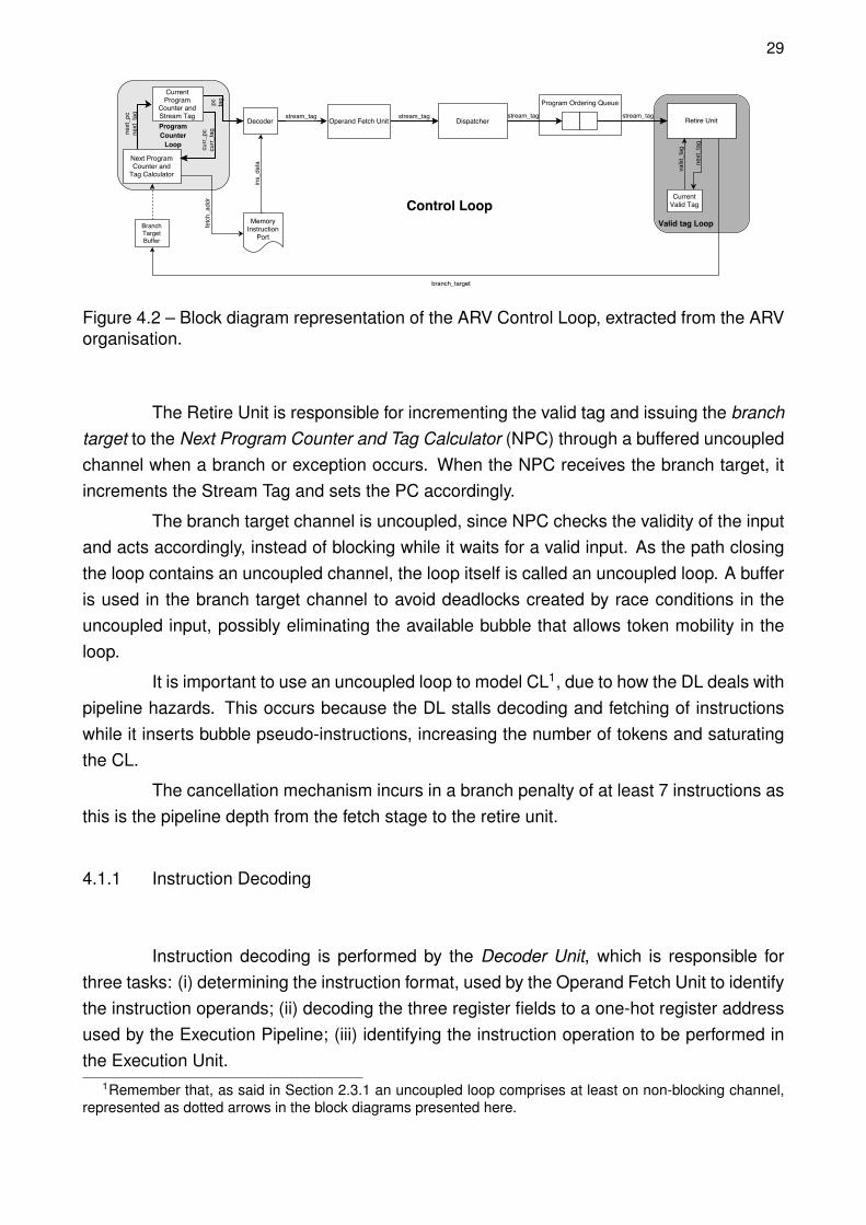
Figure 4.2 – Block diagram representation of the ARV Control Loop, extracted from the ARVorganisation.
The Retire Unit is responsible for incrementing the valid tag and issuing the branchtarget to the Next Program Counter and Tag Calculator (NPC) through a buffered uncoupledchannel when a branch or exception occurs. When the NPC receives the branch target, itincrements the Stream Tag and sets the PC accordingly.
The branch target channel is uncoupled, since NPC checks the validity of the inputand acts accordingly, instead of blocking while it waits for a valid input. As the path closingthe loop contains an uncoupled channel, the loop itself is called an uncoupled loop. A bufferis used in the branch target channel to avoid deadlocks created by race conditions in theuncoupled input, possibly eliminating the available bubble that allows token mobility in theloop.
It is important to use an uncoupled loop to model CL1, due to how the DL deals withpipeline hazards. This occurs because the DL stalls decoding and fetching of instructionswhile it inserts bubble pseudo-instructions, increasing the number of tokens and saturatingthe CL.
The cancellation mechanism incurs in a branch penalty of at least 7 instructions asthis is the pipeline depth from the fetch stage to the retire unit.
4.1.1 Instruction Decoding
Instruction decoding is performed by the Decoder Unit, which is responsible forthree tasks: (i) determining the instruction format, used by the Operand Fetch Unit to identifythe instruction operands; (ii) decoding the three register fields to a one-hot register addressused by the Execution Pipeline; (iii) identifying the instruction operation to be performed inthe Execution Unit.
1Remember that, as said in Section 2.3.1 an uncoupled loop comprises at least on non-blocking channel,represented as dotted arrows in the block diagrams presented here.
30
The instruction format is encoded in a one-hot representation with seven possi-ble values: (i) opFormatR is used for most register-to-register instructions, it instructs theOperand Fetch Unit to retrieve two operands from the register bank; (ii) opFormatI is a theformat used by the variant of register-to-register instructions that includes a 12-bit signedimmediate. The Operand Fetch Unit is instructed to fetch one operand from the registerbank and to sign-extend the immediate value embedded in the instruction as the secondoperand; (iii) opFormatS is the format used by the memory store instructions. It tells theOperand Fetch Unit to retrieve two register operands and sign extend the 12-bit immediateoffset value; (iv) opFormatB is used for conditional branch instructions. Here, the OperandFetch Unit is instructed to read two operands from registers and sign extend the 12-bit jumpoffset; (v) opFormatU is used by LUI and AUIPC and consists in sign-extending the 20-bitimmediate as one operand and using the instruction PC as the other; (vi) opFormatJ issimilar to opFormatU, but the sign-extension of the 20-bit immediate is specific to the JALinstruction; (vii) opFormatNop is used by the decoder on invalid and the optional FENCEinstructions. It signals the Operand Fetch Unit to insert a bubble.
The instruction operation is encoded in two one-hot variables. The first encodeswhich execution unit is responsible for executing the instruction. The second variable isspecific to the execution unit and encodes what operation should the latter perform on thereceived operands.
This simplifies the design of further stages, since the required control informationregarding the instruction is already decoded and readily available.
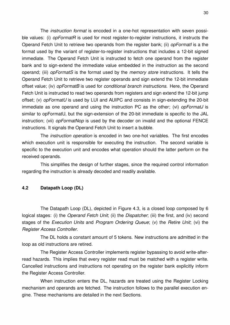
4.2 Datapath Loop (DL)
The Datapath Loop (DL), depicted in Figure 4.3, is a closed loop composed by 6logical stages: (i) the Operand Fetch Unit; (ii) the Dispatcher; (iii) the first, and (iv) secondstages of the Execution Units and Program Ordering Queue; (v) the Retire Unit; (vi) theRegister Access Controller.
The DL holds a constant amount of 5 tokens. New instructions are admitted in theloop as old instructions are retired.
The Register Access Controller implements register bypassing to avoid write-after-read hazards. This implies that every register read must be matched with a register write.Cancelled instructions and instructions not operating on the register bank explicitly informthe Register Access Controller.
When instruction enters the DL, hazards are treated using the Register Lockingmechanism and operands are fetched. The instruction follows to the parallel execution en-gine. These mechanisms are detailed in the next Sections.
31
Figure 4.3 – Block diagram representation of the ARV Datapath Loop, extracted from theARV organisation.
4.2.1 Register Locking and Operand Fetching
The Operand Fetch Unit is the entry point of instructions into the DL. This unitis responsible for retrieving data from the Register Access Controller and for completingimmediate operands. It is also responsible for stalling the pipeline in case of data hazards.
Data hazards are avoided by locking registers that are waiting for data to be writ-ten. If an instruction attempts to read a locked register, the Operand Fetch Unit stalls thedecoding of new instructions and inserts bubbles in the pipeline.
The Register Locking Loop (RLL), detailed in Figure 4.4, is responsible for trackingcurrently locked registers. It is composed by a 4-stage Target Register Queue, an OR logicalstage and the Operand Fetch Unit. The DL and RLL are closed loops of the same length,running in parallel. Every token in the RLL corresponds to a token in the DL.
Each stage in the Target Register Queue holds the target register of an instructionin execution stages: Stage 0 holds the target register of the instruction currently in theDispatcher Unit; Stages 1 and 2 holds the target register of the two instructions presentin Execution Units; and Stage 3 holds the target register of the instruction in the Retire Unit.The Target Register queue is fed by the Operands Fetch Unit and consumed by the RegisterAccess Controller.

32
Figure 4.4 – Block diagram detailing the Register Locking Loop and the Operand Fetchmechanism.
Register Addresses employs a one-hot code, which allows the use of a simple ORto sum all registers in the Target Register Queue to produce the Locked Register Mask. Thisis employed by the Operand Fetch Unit to determine whether the register the instruction iscurrently attempting to read is currently locked. If any of the registers being read are locked,the Operand Fetch Unit stalls fetching and decoding of instructions, by not handshaking withits input channel. It then inserts bubbles in the pipeline that behave like no-operation (NOP)instructions until the register in question is unlocked.
The insertion of bubble pseudo-instructions is important: (i) to avoid stalling RLL,since the OR logical stage uses channels to feed all stages of the Target Register Queue,it must be always full to generate a mask; (ii) to keep the correlation of an address in theTarget Register Queue with an instruction in some execution stage; (iii) to allow correctoperation of the Register Access Controller, which synchronises read and write operationsto the Register Bank.
The Operand Fetch Unit retrieves register operands using two register read portsin the Register Access Controller. Each read port comprises a register address channel anda register data channel. The diagram shown in Figure 4.4 aggregates the address channelsand the data channels in a single entity for the sake of simplifying the Figure.
To avoid write-after-read hazards of instructions concurrently operating on the reg-ister bank, a register read is always matched with a register write. If the address of theregister being written is equal to the address of a register being read, data is bypassed fromthe write port to the matching read ports, while register write takes place simultaneously.
This synchronisation implies that instructions not reading from registers should in-form this to the Register Access Controller, by sending a special no read code instead of a

33
register address. The no read code clears the responsibility of sending register data fromthe Register Access Unit to the Operand Fetch Unit.
The Operand Fetch Unit is also responsible for sign-extending immediate valuesfrom fields of an instruction code, according to the ISA specification.
Once all operands are retrieved, the instruction follows to the Dispatcher for execu-tion.
4.2.2 Parallel Execution and Instruction Retiring
Once an instruction enters the Dispatcher, it has all required operands available tocomplete execution. The pipeline uses a fan-out distribution characteristic of asynchronouscircuits. Instructions are only sent to units involved in their execution. This diverges fromthe traditional ALU design of synchronous processors, where data is sent to all units andresults are collected by a multiplexer. An interesting aspect of this approach is the potentialfor energy saving, since units not operating on an instruction need not produce switchingactivity.
Figure 4.5 – Block diagram representation of the ARV parallel execution engine with theinstruction Dispatcher and Retire Unit, extracted from the ARV organisation.

34
The fan-out unit selection scheme introduces problems when there is a discrepancyin the individual delays of distinct units. This may cause instructions to execute out of order.As consequence, instruction reordering techniques are required for correct execution.
Reordering is performed with the aid of the Program Ordering Queue. When theDispatcher issues an instruction to one of the execution units, it records which unit wasselected along with the stream tag in the Program Ordering Queue.
Since an instruction reordering mechanism is used, it becomes simple to imple-ment parallel execution units to improve throughput. To achieve a theoretical best case of2-instruction parallelism, the Program Ordering Queue is two-stage deep. Besides, to ac-commodate the scenario of two instructions being dispatched to a same Execution Unit insequence, units are each two-stage long.
Execution itself is carried by six parallel specialised Execution Units: (i) the BypassBuffers, simply send the single input from operand to the result output; (ii) the Adder Stagesimplement addition, subtraction and comparison operations in two stages; (iii) the LogicStage performs the bit-wise XOR, AND and OR operations; (iv) the Shifter Stage is a barrelshifter capable of arithmetic right, logic right and left shifts; (v) the Branch Stages computethe target PC and perform comparisons to determine if the branch is to be taken; (vi) theMemory Stages compute memory access addresses, command the memory access portsand sign-extend the returned data. Each execution unit operates on data, holding the resultsfor collection by the Retire Unit.
The Memory Stages are responsible for memory reads and writes. Access is per-formed using a read-then-write memory port, allowing future implementation of atomic mem-ory instructions.
A memory read operation is performed with the following steps: (i) Memory Stage1 calculates the memory access address from the base and offset values; (ii) The desiredoperation is sent to Memory Stage 2; (iii) Concurrently, the address and a flag indicating aread-only operation are sent to Memory Data Port; (iv) Memory Stage 2 receives the datafrom Memory Data Port, sign-extends it accordingly and holds the result for later collectionby the Retire Unit.
Memory write operations follow the basic flow of a memory read with slight modi-fications: (i) Memory Stage 1 is responsible for calculating the memory access address; (ii)The desired operation is also sent to Memory Stage 2; (iii) Concurrently the address, data ana flag indicating the write intention are sent to the Memory Data Port; (iv) The memory dataport is blocked, waiting for a write enable command to perform the memory write operation;(v) Memory Stage 2 then holds a flag indicating a memory write is pending for collection bythe Retire Unit; (vi) The Retire Unit eventually collects the flag and sends the write enable tothe Memory Data Port, enabling the pending memory write and completing the operation.

35
The Retire Unit reorders instructions by collecting results from the Execution Unitsin the order determined by the Program Ordering Queue. The mechanism described inSection 4.1 determines if the instruction is cancelled or not. If the instruction has not beencancelled, the Retire Unit performs the following operations depending on the instructionreceived: (i) sends the result to the Register Access Controller for writing back to the targetregister; (ii) authorises a pending memory write in the Memory Data Port; (iii) incrementsthe valid tag value and sends the branch target to the NPC.
For the register writeback, the Register Access Controller receives the result fromthe Retire Unit and writes it to the register addressed by the tail of the Target Register Queue.A register write enable channel is used to signal the Register Access Controller if the writeshould be performed or not. On an instruction cancellation, the flag is set low and the resultis ignored by the Register Access Controller. This is necessary to synchronise the RLL andthe DL since the target register address is consumed from the Target Register Queue onlywhen the Retire Unit finishes the instruction execution.
4.3 Initialisation
All sequential circuits require some initialisation to a known starting state. SinceARV comprises closed loops, the initialisation process must place tokens in the correct logi-cal stages to fill the loops. This guarantees a stable and expected start of operation.
Figure 4.6 – Block diagram representation of the ARV organisation, with logical units ini-tialised with tokens highlighted in dark grey.
The logical stages marked with dark grey in Figure 4.6 must be initialised withtokens. Stages not marked are initialised to a empty state, waiting for tokens in their inputs.

36
The Next Program Counter and Tag Calculator is initialised with the initial ProgramCounter value. This initiates the fetching of instructions.
The DL and RLL must be initialised with tokens for correct operation. The tokensplaced initialise the DL to a state where it is full of bubbles, each acting as an NOP instruc-tion. The Stream Tag of the bubbles is set to 0, but they are irrelevant, since bubbles committo neither memory or registers, nor they modify the program counter.
The Stream Tag and Valid Tag values are set by the NPC and the Retire Unit to 0on initialisation. The PC is set to 0 and the first instruction is fetched from memory location0.
37
5. THE ARV ORGANISATION MODELLING AND VALIDATION
The ARV organisation was modelled using the Go programming language, applyingtechniques like those described in Section 2.3.1. The model is executable and acts as asimulator capable of running code compiled for the RISC-V 32-bit integer architecture, theRV32I ISA. This approach allows the use of software tools to detect race conditions anddeadlocks, making it easier to correct the design.
This Chapter describes how the processor and the simulation platform was mod-elled using Go, the software used for validation, how the software is executed in the simu-lated platform and how validation in Go may help in designing complex circuits.
5.1 The ARV Go Model and Simulator
The processor model is composed of a series of goroutines communicating throughchannels and a model object holding persistent information about the state of the model.The model object holds reference to the memory model used by the simulated processor,the register bank and a flag used to synchronise the start of simulation after the model isconstructed.
The model components are initiated by a set of hierarchical constructors. Eachconstructor is responsible for creating the goroutine representing the logical stages and thechannels connecting logical stages. The goroutines are instantiated using inline anonymousfunctions.
The topmost constructor initialises the state structure and the channels intercon-necting the stages before calling child constructors. Each constructor is responsible forlaunching goroutines implementing the logical stage.
Logical stages that initialise to a specific state, as described in Section 4.3 wait forthe common start flag before sending initial data to the channel. This guarantees that uponconstruction the model waits for a start signal before operating.
The processor model constructor expects a memory model reference as argument.This is an object providing constructors for the memory read and write ports that creategoroutines behaving as memory access ports.
The memory model adopted in simulation accesses a memory mapped file anda simulated register for controlling the simulation. A file is mapped using the mmap systemcall of Unix operation systems to the beginning of the memory address, starting at address0x0. The upper memory area is reserved for two simulated register that control the simu-lation platform: (i) When writing to address range 0x80001000-0xFFFFFFFF, all bytes are

38
interpreted as characters and outputted to the terminal; (ii) Writing any value to address0x80000000 terminates the simulation.
To aid debugging, the instruction flow in the pipeline can be logged to the output.This behaviour is optionally enabled by setting a flag when invoking the platform.
The model and simulation platform are all written in Go and it is expected fromthe reader willing to use the platform to have available a proper working Go developmentenvironment. The Go package name is bitbucket.org/marcos_sartori/qdi-riscv and itis beyond the scope of this work describing how to install and compile Go packages andtheir dependencies. Instructions on how to install and use the Go environment can be foundin the official documentation (https://golang.org/doc).
It is worth noting that due to the use of the mmap system call, the simulation isadapted to only run in Unix-like platforms. The version described herein has been success-fully validated and tested using Go version 1.7.5 on Fedora 25 and Go 1.8.1 on Ubuntu 16.04LTS.
5.2 Validation Software
The validation was performed using software compiled for RV32I architecture. Aport of the RISC-V Foundation unit tests for RISC-V processors is used to test conformityto the RISC-V ISA [RIS15b]. A port of bareOS for the RISC-V, a minimalist baremetal Cruntime and library used by Aguiar, Moratelli, Sartori et al. to validate a hypervisor for MIPS-based MPSoCs [AMSH13] was also used to test ARV’s capability to run code generated byhigh-level compilers.
The unit test for RISC-V is a set of assembly programs designed to test individualinstruction compliance to the RISC-V specifications. It tests general and corner cases foreach instruction, comparing the execution result to an expected value.
The code itself is written using assembly macros and it can be easily ported todifferent execution environments by modifying stubs implementing communication with theoutside world and linking to the appropriated memory location. The unit test used targetRV32I, the basic subset of the ISA, which is implemented in the proposed organisation.
To further validate the processor, code generated by a C compiler is used. Sincethe simulation environment has no operating system, bareOS was ported to the RISC-V ar-chitecture. It is responsible for interfacing with the hardware. It initialises a sane C executionenvironment expected by GCC and provides support libraries, including a basic C libraryand software multiply functions.
A small application in C implementing a non-recursive resolution algorithm to solvethe Tower of Hanoi problem was compiled for bareOS and used for compiled code validation.

39
This application was chosen due to its use of branches, function calls and memory accesses,being similar to a regular structured memory-bound application. This tests aims at stressingthe pipeline to check for bugs in the branching and hazard avoidance mechanism.
5.3 Running Code on the Simulated Platform
The platform runs real code placed into its memory starting at address 0. All gen-eral purpose registers start with an unknown value. To run software on the platform, theobject code must be preloaded to the required position in a flat binary file representing thememory contents and it should perform any initialisation of the environment.
Also a tool chain capable of generating code for the RISC-V architecture is requiredto compile code for the platform. In this work, the official The RISC-V Foundation Toolchainis used to generate code [RIS15a]. Instructions to download and compile this tool chain canbe found at https://github.com/riscv/riscv-gnu-toolchain.
Since ARV does not implement the 64-bit variant of the ISA which is built by default,it is important to use the following commands to build the compiler once its source code isdownloaded:
$ mkdir build
$ cd build
$ ../configure --with-arch=rv32ima --with-abi=ilp32
$ sudo make
These steps build and install the riscv32 Toolchain in the /usr/local prefix, elimi-nating the requirement to adjust PATH variables.
Directory samplecode in the source code distribution contains: (i) a copy of bareOS,responsible for initialising the C execution environment; (ii) a linker script, defining the mem-ory layout; (iii) a makefile which invokes the compiler and strips the binary headers to createthe required flat memory image required by the Simulation Platform.
New code can be easily ported to the platform using bareOS. File dummy.c providesa template for new projects, it contains function kmain which should never return and is calledonce the C runtime environment finishes initialisation. Function halt provides a clean wayof finishing execution.
To compile and run new code on the platform, copy dummy.c to a new file terminat-ing in .c. Edit the file to provide the source code of the new program. Include the chosenfile name in the PROGNAME list in the Makefile, i.e. test_hannoi.c becomes test_hannoi
Running make on the samplecode directory should create a .lst and a .bin file forevery entry in PROGNAME. The .lst file is the assembly listing of the compiled program, whichhelps during debugging. Finally, the .bin file is the memory image file used by the simulator.

40
To launch the compiler in the simulator invoke qdi-riscv supplying the memoryimage file name as argument to the -memfile flag. Other flags are present and relate to theprocess of debugging the processor model. Invoking compilation with -h provides a briefdescription on how to use them.
5.4 Advantages of Using Go for Asynchronous Circuit Validation
The main advantage of using Go when designing complex asynchronous circuitsis the easy detection and visualisation of deadlock conditions at the message passing ab-straction level. This helps in managing complexity, since predicting deadlock conditions atearly design stages can be difficult. This occurs due to the high parallelism of asynchronouscircuits and the interaction of units at the system level leading to unexpected scenarios.
Once a deadlock condition occurs, the state of each goroutine is displayed in anon-screen panic trace. The panic trace shows the state of each goroutine, if it is lockedwaiting to send or receive on a channel and the line of code it is currently locked on. Thisinformation is enough to identify in the source code the goroutines involved in the productionof a deadlock.
If further information about the state of the program is required when the deadlockoccurs, logging instructions can be inserted in the source code to examine the executionflow in key goroutines.
To demonstrate it, a step of the validation where design changes were introduceddue to a deadlock condition is presented herein. The deadlock occurred due to the CLsaturation that occurred intermittently on branch instructions. The cause was identified tobe a race condition on the uncoupled branch target channel from the Retire Unit to theNPC. The solution was the introduction of a buffer stage on the output of the Retire Unit toaccommodate the token during extra handshake cycles without locking the Retire Unit.
Appendix A.1 includes the panic trace for the described deadlock. A designer fa-miliar with the organisation knows how units are connected. He can then look at the stateof goroutines to identify the nature of the deadlock. In the example, all stages of the Con-trol Loop are locked in send operations, meaning that it is saturated. The Retire Unit ingoroutine 38 is blocked sending the branch target, while the NPC is blocked trying to sendthe next PC value to the memory instruction port. The expected behaviour is that the NPCshould receive the branch target if one is available, before trying to fetch the next instruction.However, a race condition occurred and the NPC advanced, inserting a token that saturatesthe control loop. To solve the problem, a buffer stage is inserted to hold the branch target,effectively inserting a second bubble in the loop to accommodate the token inserted whenthe race condition occurs.

41
6. RESULTS AND FINAL THOUGHTS
This Chapter presents the result of each test and briefly discusses them. Later,it discusses the merits and shortcomings of this work, followed by the proposition of futurework to continue, extend and/or improve this initial work.
6.1 Validation Results
After iterations of validation and corrections, the developed model passed all pro-posed tests. This Section presents and discuses the results.
The results mentioned in this Section are the output of the simulation platform foreach test. It includes messages from the simulation platform and the output of the programrunning in the simulated environment. At the end, metrics of the execution regarding pipelineusage are shown.
6.1.1 Unit Test for RISC-V Processors
The Unit Test for RISC-V Processors checks the processors compliance to theRISC-V ISA specification. The simulator output in Appendix A.2 shows the results for thecompliance test to the RV32I subset of the ISA.
Each instruction is tested for compliance and OK or ERROR is printed to indicatewhether it passed or failed the test. The proposed organisation passed every individualinstruction test, indicating compliance to the ISA specification. However, compliance to thestandard does not guarantee the processor is free of bugs.
The performance at first appears sub-optimal, with 17,285 bubbles inserted due topipeline hazards for 14,729 decoded instructions. Instruction cancellation due to branchesalso display a relatively high figure of 6,588 instructions for a simple assembly program, butthis is expected, since no branch prediction mechanism was implemented.
6.1.2 High Level Compiled Code
The Tower of Hanoi test further stresses the pipeline and certifies the correct exe-cution of compiled C code. The simulator output in Appendix A.3 shows the computed stepsrequired to solve the Tower of Hanoi puzzle.

42
It computes the 127 steps required to solve the puzzle with 7 disks, with rods num-bered from 0 to 2. The code calls printf routine to print the instructions of each step aftercalculating the move. This test uses memory accesses and function calls extensively. Thisstresses the branch, hazard-avoidance and memory access mechanisms.
To assert correction execution, the test program was compiled and run for both thesimulated and host platforms and their outputs were compared. The outputs were identical,proving that the design is capable of correctly executing software compiled for the RISCV32IISA.
The performance was again sub-optimal, inserting 145,835 bubbles for 154,943 de-coded instructions to avoid pipeline hazards. Instruction cancellation accounted for 125,920instructions and bubbles reaching the Retire Unit, with 174,856 instructions completing exe-cution.
6.2 Conclusion and Future Works
This work satisfied its goal of implementing a high-level functional model of the ARVasynchronous processor. Validation results strongly indicate that the ARV model correctlyimplements the RISC-V RV32I architecture.
The design and high-level model of ARV in Go have proved the language is ad-equate to model complex handshake channel-based circuits. The software environmentprovided by the language helped during the design debugging process. The author be-lieves the advantages of using a high level language for validation justify the use of the Goprogramming language as a hardware description language.
Of course, to implement hardware modelled in Go, it is necessary to develop tech-niques to translate the Go high level description to lower level descriptions. Future workincludes developing tools to automatically transform the high level Go description into alower level netlist using asynchronous templates.
Performance of the described implementation seems rather poor at first, albeit noprecise timing measurements can in fact be extracted as the model proposed contains noteven delay estimations. Future work is also expected to improve the pipeline performanceby exploring optimisation techniques such as hazard resolution units, out-of-order executionand branch prediction units.
The preliminary instruction cancellation measurements presented in this work stronglyindicate the need for a branch prediction unit as a primary organisation optimisation. Due tothe nature of asynchronous circuits, the cost of bubbles need to be evaluated, comparing itto the cost of implementing alternative solutions.

43
The timing analysis required for performance evaluation depends upon proposinga more detailed model, with features that allow estimating signal propagation delays. Suchfiner-grain models are the target of future work, and will be developed with the aid of asyn-chronous templates and specific standard-cell level descriptions. A finer-grain timed modelwill also allow the use of industry standard benchmarks to estimate performance.
The Author is currently continuing this work, to explore the necessary steps toimplement the organisation proposed here in silicon using asynchronous design techniques.

44
REFERENCES
[AAB+16] Asanovic, K.; Avizienis, R.; Bachrach, J.; Beamer, S.; Biancolin, D.; Celio, C.;Cook, H.; Dabbelt, D.; Hauser, J.; Izraelevitz, A.; Karandikar, S.; Keller, B.; Kim,D.; Koenig, J.; Lee, Y.; Love, E.; Maas, M.; Magyar, A.; Mao, H.; Moreto, M.; Ou,A.; Patterson, D. A.; Richards, B.; Schmidt, C.; Twigg, S.; Vo, H.; Waterman, A.“The rocket chip generator”, Technical Report UCB/EECS-2016-17, University ofCalifornia, Berkeley, 2016, 11p.
[AMSH13] Aguiar, A.; Moratelli, C.; Sartori, M. L. L.; Hessel, F. “A virtualization approachfor MIPS-based MPSoCs”. In: International Symposium on Quality ElectronicDesign (ISQED), 2013, pp. 611–618.
[AP14] Asanovic, K.; Patterson, D. A. “Instruction Sets Should Be Free: The Casefor RISC-V”, Technical Report UCB/EECS-2014-146, University of California,Berkeley, 2014, 7p.
[BOF10] Beerel, P.; Ozdag, R. O.; Ferretti, M. “A Designer´s Guide to AsynchronousVLSI”. Cambridge University Press, 2010, 353p.
[Cel16] Celio, C. “ccelio/riscv-boom-doc Github repository”. Source: https://github.com/ccelio/riscv-boom-doc, 2017-06-30.
[EB02] Edwards, D.; Bardsley, A. “Balsa: An asynchronous Hardware SynthesisLanguage”, The Computer Journal, vol. 45–1, 2002, pp. 12–18.
[FDG+94] Furber, S. B.; Day, P.; Garside, J. D.; Paver, N. C.; Woods, J. V. “AMULET1: amicropipelined ARM”. In: Compcon, 1994, pp. 476–485.
[FEG00] Furber, S. B.; Edwards, D. A.; Garside, J. D. “AMULET3: A 100 MIPSAsynchronous Embedded Processor”. In: IEEE International Conference onComputer Design (ICCD), 2000, pp. 329–334.
[FGT+97] Furber, S. B.; Garside, J. D.; Temple, S.; Liu, J.; Day, P.; Paver, N. C.“AMULET2e: An Asynchronous Embedded Controller”. In: InternationalSymposium on Advanced Research in Asynchronous Circuits and Systems(ASYNC), 1997, pp. 290–299.
[Fur95] Furber, S. “Computing without Clocks: Micropipelining the ARM Processor”.London: Springer London, 1995, chap. 5, pp. 211–262.
[GFTW09] Garside, J. D.; Furber, S. B.; Temple, S.; Woods, J. V. “The AmuletChips: Architectural Development for Asynchronous Microprocessors”. In: IEEE

45
Internation Conference on Electronics, Circuits and Systems (ICECS), 2009, pp.343–346.
[Goo12] Google Inc. “The Go Programming Language”. Source: https://golang.org, 2017-05-22.
[Hoa78] Hoare, C. A. R. “Communicating Sequential Processes”, Communications of theACM, vol. 21–8, Aug 1978, pp. 666–677.
[Hoa85] Hoare, C. A. R. “Communicating Sequential Processes”. Prentice HallInternational, 1985, 260p.
[low15] lowRisc. “Rocket Core Overview”. Source:http://www.lowrisc.org/docs/untether-v0.2/rocket-core/,2017-06-30.
[LWA+14] Lee, Y.; Waterman, A.; Avizienis, R.; Cook, H.; Sun, C.; Stojanovic, V.; Asanovic,K. “A 45nm 1.3 GHz 16.7 Double-Precision GFLOPS/W RISC-V Processor withVector Accelerators”. In: European Solid State Circuits Conference (ESSCIRC),2014, pp. 199–202.
[Mar90] Martin, A. J. “The Limitations to Delay-Insensitivity in Asynchronous Circuits”. In:6th MIT Conference on Advanced Research in VLSI, 1990, pp. 263–278.
[Mar14] Martin, A. “25 Years Ago: The First Asynchronous Microprocessor”, TechnicalReport CaltechAUTHORS:20140206-111915844, California Institute ofTechnology (CALTECH), 2014, 12p.
[MBL+89] Martin, A. J.; Burns, S. M.; Lee, T. K.; Borkovic, D.; Hazewindus, P. J.“The Design of an Asynchronous Microprocessor”, ACM SIGARCH ComputerArchitecture News (SIGARCH), vol. 17–4, 1989, pp. 99–110.
[MLM+97] Martin, A. J.; Lines, A. M.; Manohar, R.; Nyström, M.; Penzes, P.; Southworth,R.; Cummings, U.; Lee, T. K. “Design of an Asynchronous MIPS R3000Microprocessor”. In: Conference on Advanced Research in VLSI (ARVLSI),1997, pp. 164–181.
[MLM+02] Martin, A. J.; Lines, A.; Manohar, R.; Cummings, U.; Nyström, M. “PipelinedAsynchronous Processing”. US Patent US6381692 B1, Source: https://www.google.ch/patents/US6381692, Dec 2 2002.
[MNW03] Martin, A. J.; Nyström, M.; Wong, C. G. “Three Generations of AsynchronousMicroprocessors”, IEEE Design & Test of Computers, vol. 20–6, 2003, pp. 9–17.
46
[PD80] Patterson, D. A.; Ditzel, D. R. “The Case for the Reduced Instruction SetComputer”, ACM SIGARCH Computer Architecture News (SIGARCH), vol. 8–6, Oct 1980, pp. 25–33.
[PP16] Prasertsang, A.; Pradubsuwun, D. “Formal Verification of Concurrency in Go”.In: Joint Conference on Computer Science and Software Engineering (JCSSE),2016, pp. 1–4.
[RIS15a] RISC-V Foundation. “GNU Toolchain for RISC-V, including GCC 7.1.0”. Source:https://github.com/riscv/riscv-gnu-toolchain, 2017-06-05.
[RIS15b] RISC-V Foundation. “Unit Tests for RISC-V Processors”. Source: https://github.com/riscv/riscv-tests, 2017-06-01.
[SF01] Sparsø, J.; Furber, S. “Principles of Asynchronous Circuit Design – A SystemsPerspective”. Springer, 2001, 356p.
[Sut89] Sutherland, I. E. “Micropipelines”, Communications of the ACM, vol. 32–6,Jun 1989, pp. 720–738.
[UoC14] University of California, B. “ucb-bar/riscv-sodor Github repository”. Source:https://github.com/ucb-bar/riscv-sodor/wiki, 2017-06-30.
[vBKR+91] van Berkel, K.; Kessels, J.; Roncken, M.; Saeijs, R.; Schalij, F. “The VLSI-programming language Tangram and its Translation into Handshake Circuits”.In: European Conference on Design Automation (DATE), 1991, pp. 384–389.
[Ver88] Verhoeff, T. “Delay-Insensitive Codes - An Overview”, Distributed Computing,vol. 3–1, Mar 1988, pp. 1–8.
[WLPA16] Waterman, A.; Lee, Y.; Patterson, D. A.; Asanovic, K. “The RISC-VInstruction Set Manual, Volume I: User-Level ISA, Version 2.1”, Technical ReportUCB/EECS-2016-118, University of California, Berkeley, 2016, 133p.
[XN16] Xie, J.; NVIDIA. “NVIDIA RISC-V Evaluation Story”. In: RISC-V Workshop, 2016,pp. 1–15.

47
APPENDIX A – SIMULATION OUTPUT
A.1 Deadlock panic trace
2017/06/05 19:07:42 Memdump file opened
2017/06/05 19:07:42 Memory model created from file
2017/06/05 19:07:42 Processor model instantiated
2017/06/05 19:07:42 Simulation started
lui..OK
fatal error: all goroutines are asleep - deadlock!
goroutine 1 [chan receive]:
main.main
main.go:61
goroutine 5 [chan send]:
processor.(*processor).nextPcUnit.func1
processor/fetch.go:42
created by processor.(*processor).nextPcUnit
processor/fetch.go:46
goroutine 6 [chan send]:
processor.(*processor).fetchUnit.func1
processor/fetch.go:71
created by processor.(*processor).fetchUnit
processor/fetch.go:73
goroutine 7 [chan send]:
processor.(*processor).fetchUnit.func2
processor/fetch.go:81
created by processor.(*processor).fetchUnit
processor/fetch.go:83
goroutine 8 [select]:
processor.(*processor).fetchUnit.func3
processor/fetch.go:88
created by processor.(*processor).fetchUnit
processor/fetch.go:94

48
goroutine 9 [chan send]:
memory.(*memoryArray).ReadPort.func1
memory/memory.go:61
created by memory.(*memoryArray).ReadPort
memory/memory.go:66
goroutine 10 [chan send]:
processor.(*processor).decoderUnit.func1
processor/decoder.go:266
created by processor.(*processor).decoderUnit
processor/decoder.go:268
goroutine 11 [chan send]:
processor.(*processor).operandFetchUnit.func1
processor/operandfetch.go:96
created by processor.(*processor).operandFetchUnit
processor/operandfetch.go:211
goroutine 12 [chan receive]:
processor.(*processor).reglockEl.func1
processor/registerlock.go:19
created by processor.(*processor).reglockEl
processor/registerlock.go:23
goroutine 13 [chan send]:
processor.(*processor).reglockEl.func1
processor/registerlock.go:20
created by processor.(*processor).reglockEl
processor/registerlock.go:23
goroutine 14 [chan send]:
processor.(*processor).reglockEl.func1
processor/registerlock.go:20
created by processor.(*processor).reglockEl
processor/registerlock.go:23
goroutine 15 [chan send]:
processor.(*processor).reglockEl.func1
processor/registerlock.go:20

49
created by processor.(*processor).reglockEl
processor/registerlock.go:23
goroutine 16 [chan receive]:
processor.(*processor).registerLock.func1
processor/registerlock.go:61
created by processor.(*processor).registerLock
processor/registerlock.go:69
goroutine 17 [chan receive]:
processor.(*regFile).WritePort.func1
processor/registerbank.go:38
created by processor.(*regFile).WritePort
processor/registerbank.go:50
goroutine 18 [chan receive]:
processor.(*regFile).ReadPort.func1
processor/registerbank.go:19
created by processor.(*regFile).ReadPort
processor/registerbank.go:32
goroutine 19 [chan receive]:
processor.(*regFile).ReadPort.func1
processor/registerbank.go:19
created by processor.(*regFile).ReadPort
processor/registerbank.go:32
goroutine 20 [chan receive]:
processor.(*processor).registerBypass.func1
processor/registerbypass.go:44
created by processor.(*processor).registerBypass
processor/registerbypass.go:96
goroutine 21 [chan send]:
processor.(*processor).dispatcherUnit.func1
processor/dispatcher.go:92
created by processor.(*processor).dispatcherUnit
processor/dispatcher.go:95
goroutine 22 [chan send]:

50
processor.(*processor).bypassEl.func1
processor/bypassunit.go:14
created by processor.(*processor).bypassEl
processor/bypassunit.go:16
goroutine 23 [chan send]:
processor.(*processor).bypassEl.func1
processor/bypassunit.go:14
created by processor.(*processor).bypassEl
processor/bypassunit.go:16
goroutine 24 [chan send]:
processor.(*processor).prgQElement.func1
processor/programqueue.go:42
created by processor.(*processor).prgQElement
processor/programqueue.go:44
goroutine 25 [chan send]:
processor.(*processor).prgQElement.func1
processor/programqueue.go:42
created by processor.(*processor).prgQElement
processor/programqueue.go:44
goroutine 26 [chan send]:
processor.(*processor).adderUnit.func1
processor/adder.go:17
created by processor.(*processor).adderUnit
processor/adder.go:19
goroutine 27 [chan receive]:
processor.(*processor).adderUnit.func2
processor/adder.go:23
created by processor.(*processor).adderUnit
processor/adder.go:43
goroutine 28 [chan receive]:
processor.(*processor).logicUnit.func1
processor/logicunit.go:16
created by processor.(*processor).logicUnit
processor/logicunit.go:19

51
goroutine 29 [chan receive]:
processor.(*processor).logicUnit.func2
processor/logicunit.go:23
created by processor.(*processor).logicUnit
processor/logicunit.go:33
goroutine 30 [chan receive]:
processor.(*processor).shifterUnit.func1
processor/shiftUnit.go:16
created by processor.(*processor).shifterUnit
processor/shiftUnit.go:19
goroutine 31 [chan receive]:
processor.(*processor).shifterUnit.func2
processor/shiftUnit.go:24
created by processor.(*processor).shifterUnit
processor/shiftUnit.go:34
goroutine 32 [chan receive]:
memory.(*memoryArray).ReadWritePort.func1
memory/memory.go:79
created by memory.(*memoryArray).ReadWritePort
memory/memory.go:130
goroutine 33 [chan receive]:
processor.(*processor).memoryUnit.func1
processor/memoryunit.go:39
created by processor.(*processor).memoryUnit
processor/memoryunit.go:70
goroutine 34 [chan receive]:
processor.(*processor).memoryUnit.func2
processor/memoryunit.go:77
created by processor.(*processor).memoryUnit
processor/memoryunit.go:102
goroutine 35 [chan receive]:
processor.(*processor).branchUnit.func1
processor/branchunit.go:21
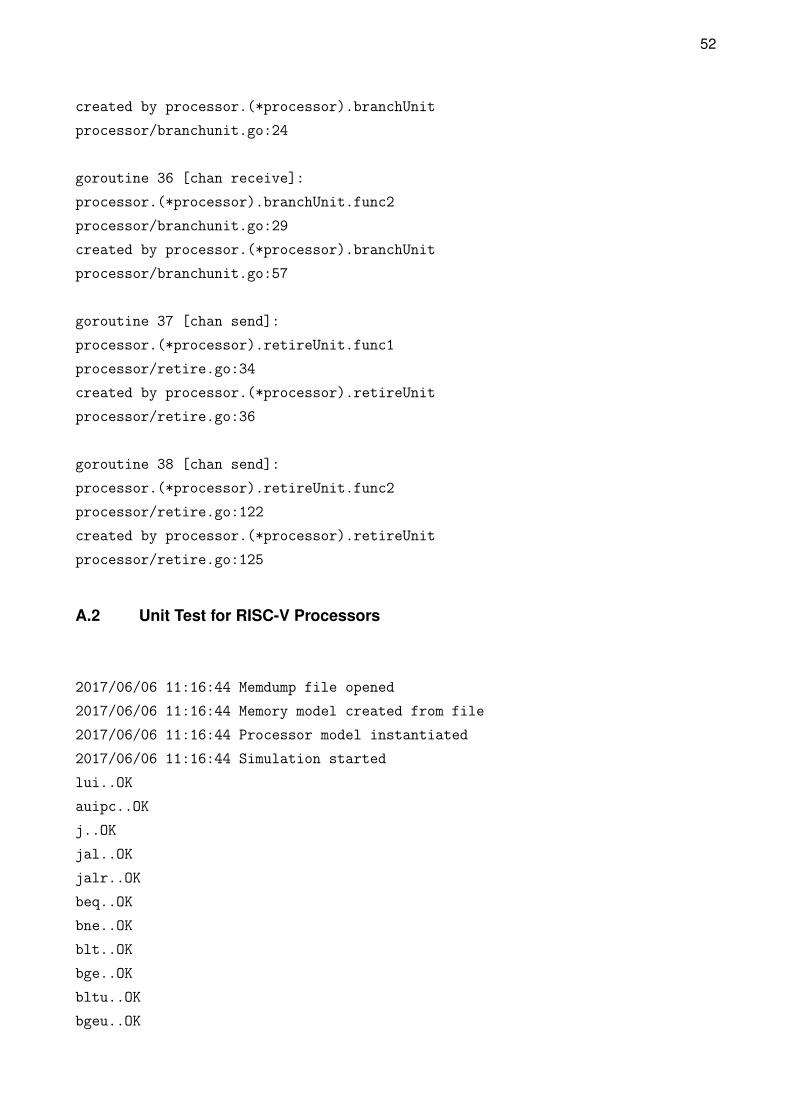
52
created by processor.(*processor).branchUnit
processor/branchunit.go:24
goroutine 36 [chan receive]:
processor.(*processor).branchUnit.func2
processor/branchunit.go:29
created by processor.(*processor).branchUnit
processor/branchunit.go:57
goroutine 37 [chan send]:
processor.(*processor).retireUnit.func1
processor/retire.go:34
created by processor.(*processor).retireUnit
processor/retire.go:36
goroutine 38 [chan send]:
processor.(*processor).retireUnit.func2
processor/retire.go:122
created by processor.(*processor).retireUnit
processor/retire.go:125
A.2 Unit Test for RISC-V Processors
2017/06/06 11:16:44 Memdump file opened
2017/06/06 11:16:44 Memory model created from file
2017/06/06 11:16:44 Processor model instantiated
2017/06/06 11:16:44 Simulation started
lui..OK
auipc..OK
j..OK
jal..OK
jalr..OK
beq..OK
bne..OK
blt..OK
bge..OK
bltu..OK
bgeu..OK

53
lb..OK
lh..OK
lw..OK
lbu..OK
lhu..OK
sb..OK
sh..OK
sw..OK
addi..OK
slti..OK
xori..OK
ori..OK
andi..OK
slli..OK
srli..OK
srai..OK
add..OK
sub..OK
sll..OK
slt..OK
xor..OK
srl..OK
sra..OK
or..OK
and..OK
simple..OK
DONE
2017/06/06 11:16:44 Finishing Simulation
2017/06/06 11:16:44 Decoded: 14729 instructions
2017/06/06 11:16:44 Inserted: 17285 bubbles
2017/06/06 11:16:44 Retired: 25424 instructions
2017/06/06 11:16:44 Cancelled: 6588 instructions
A.3 Tower of Hanoi
2017/06/06 16:26:09 Memdump file opened
2017/06/06 16:26:09 Memory model created from file
2017/06/06 16:26:09 Processor model instantiated

54
2017/06/06 16:26:09 Simulation started
init Hanoi
Resolving Hanoi
0: Move from 0 to 2
1: Move from 0 to 1
2: Move from 2 to 1
3: Move from 0 to 2
4: Move from 1 to 0
5: Move from 1 to 2
6: Move from 0 to 2
7: Move from 0 to 1
8: Move from 2 to 1
9: Move from 2 to 0
10: Move from 1 to 0
11: Move from 2 to 1
12: Move from 0 to 2
13: Move from 0 to 1
14: Move from 2 to 1
15: Move from 0 to 2
16: Move from 1 to 0
17: Move from 1 to 2
18: Move from 0 to 2
19: Move from 1 to 0
20: Move from 2 to 1
21: Move from 2 to 0
22: Move from 1 to 0
23: Move from 1 to 2
24: Move from 0 to 2
25: Move from 0 to 1
26: Move from 2 to 1
27: Move from 0 to 2
28: Move from 1 to 0
29: Move from 1 to 2
30: Move from 0 to 2
31: Move from 0 to 1
32: Move from 2 to 1
33: Move from 2 to 0
34: Move frrm 1 to 0
35: Move from 2 to 1
36: Move from 0 to 2

55
37: Move from 0 to 1
38: Move from 2 to 1
39: Move from 2 to 0
40: Move from 1 to 0
41: Move from 1 to 2
42: Move from 0 to 2
43: Move from 1 to 0
44: Move from 2 to 1
45: Move from 2 to 0
46: Move from 1 to 0
47: Move from 2 to 1
48: Move from 0 to 2
49: Move from 0 to 1
50: Move from 2 to 1
51: Move from 0 to 2
52: Move from 1 to 0
53: Move from 1 to 2
54: Move from 0 to 2
55: Move from 0 to 1
56: Move from 2 to 1
57: Move from 2 to 0
58: Move from 1 to 0
59: Move from 2 to 1
60: Move from 0 to 2
61: Move from 0 to 1
62: Move from 2 to 1
63: Move from 0 to 2
64: Move from 1 to 0
65: Move from 1 to 2
66: Move from 0 to 2
67: Move from 1 to 0
68: Move from 2 to 1
69: Move from 2 to 0
70: Move from 1 to 0
71: Move from 1 to 2
72: Move from 0 to 2
73: Move from 0 to 1
74: Move from 2 to 1
75: Move from 0 to 2
76: Move from 1 to 0
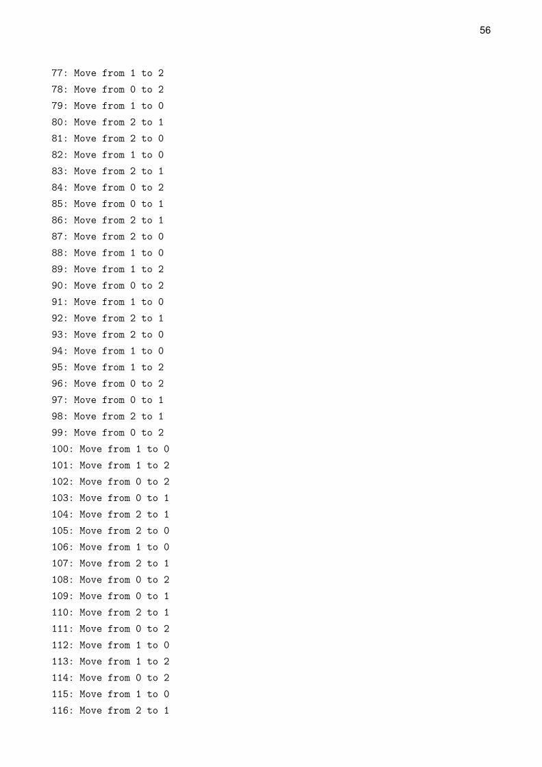
56
77: Move from 1 to 2
78: Move from 0 to 2
79: Move from 1 to 0
80: Move from 2 to 1
81: Move from 2 to 0
82: Move from 1 to 0
83: Move from 2 to 1
84: Move from 0 to 2
85: Move from 0 to 1
86: Move from 2 to 1
87: Move from 2 to 0
88: Move from 1 to 0
89: Move from 1 to 2
90: Move from 0 to 2
91: Move from 1 to 0
92: Move from 2 to 1
93: Move from 2 to 0
94: Move from 1 to 0
95: Move from 1 to 2
96: Move from 0 to 2
97: Move from 0 to 1
98: Move from 2 to 1
99: Move from 0 to 2
100: Move from 1 to 0
101: Move from 1 to 2
102: Move from 0 to 2
103: Move from 0 to 1
104: Move from 2 to 1
105: Move from 2 to 0
106: Move from 1 to 0
107: Move from 2 to 1
108: Move from 0 to 2
109: Move from 0 to 1
110: Move from 2 to 1
111: Move from 0 to 2
112: Move from 1 to 0
113: Move from 1 to 2
114: Move from 0 to 2
115: Move from 1 to 0
116: Move from 2 to 1

57
117: Move from 2 to 0
118: Move from 1 to 0
119: Move from 1 to 2
120: Move from 0 to 2
121: Move from 0 to 1
122: Move from 2 to 1
123: Move from 0 to 2
124: Move from 1 to 0
125: Move from 1 to 2
126: Move from 0 to 2
Solved Hanoi :)
2017/06/06 16:26:15 Finishing Simulation
2017/06/06 16:26:15 Decoded: 154943 instructions
2017/06/06 16:26:15 Inserted: 145835 bubbles
2017/06/06 16:26:15 Retired: 174856 instructions
2017/06/06 16:26:15 Cancelled: 125920 instructions
![Professor Lima [.·.]...Escalonamento de Processos Por sua vez, Deitel coloca que: A designação de processadores físicos para processos permite aos processos a realização de trabalho](https://img.pdfslide.us/doc/110x75/605430cf9fd731416b5eb699/professor-lima-escalonamento-de-processos-por-sua-vez-deitel-coloca-que.jpg)