Embed Size (px)
Citation preview
EPJ Appl. Metamat. 2018, 5, 3© C.A. Balanis et al., published by EDP Sciences, 2018https://doi.org/10.1051/epjam/2017010
Available online at:epjam.edp-open.org
Metamaterials'2017Metamaterials and Novel Wave Phenomena: Theory, Design and Applications
REVIEW
Applications of AMC-based impedance surfacesConstantine A. Balanis*, Mikal Askarian Amiri, Anuj Y. Modi, Sivaseetharaman Pandi, and Craig R. Birtcher
Arizona State University, Tempe, Arizona, USA
* e-mail: b
This is an O
Received: 21 September 2017 / Accepted: 29 October 2017
Abstract. The recent and major enhancements of artificial magnetic conductor (AMC) and their applicationsnamely RCS reduction, low-profile antennas and holographic leaky wave antennas are reviewed. Full-wavesimulations are compared to measurements of fabricated models, and a good agreement is attained. All of themeasurement were conducted in the Arizona State University electromagnetic anechoic chamber (EMAC).
Keywords: High impedance surface / metasurfaces / artificial magnetic conductors / RCS reduction /checkerboard surface / ultra wideband / curvilinear patches / loop antenna / spiral antenna / low-profile /superdirective / holography / leaky waves
1 Introduction
Artificial magnetic conductors (AMC) were proposed forthe first time in 1999 [1], and since then have beenextensively explored and widely used in antenna andelectromagnetics applications. These structures consist ofperiodic grid of metallic patches which are mounted on topof a thin grounded dielectric substrate. The uniqueproperty of AMCs is their in-phase reflection coefficientat a certain frequency which makes them similar tomagnetic conductors. To understand the in-phase reflec-tion mechanism, the AMC under plane wave illuminationcan be modeled as a lumped parallel LC circuit. Thecapacitance is primarily due to the fringing fields betweenadjacent patches while the inductance is basicallyattributed to the thin grounded dielectric. Since theequivalent LC model is open circuit at the resonantfrequency vr ¼ 1=
ffiffiffiffiffiffiffiLC
p, the HIS has also a high impedance
at vr similar to a PMC surface. Further analysis andmodelings of AMCs are available in [2–4].
Given that perfect magnetic conductors do not exist innature, the significance of these AMC becomes even morepivotal in some applications. Image theory indicates that aperfect magnetic conductor (PMC) surface would be anefficient candidate in the applications where the radiatingelement is very close to the ground plane, unlike a perfectelectric conductor (PEC) surface whose radiation efficiencyis very poor [5–7]. Thus, in the recent years, AMCs areconsidered a major breakthrough in antenna and electro-magnetics engineering. This paper is an attempt to review
pen Access article distributed under the terms of the Creative Comwhich permits unrestricted use, distribution, and reproduction
some of their latest applications, particularly:
–min
RCS reduction using checkerboard artificial impedancesurfaces: Conventional methods of radar cross section(RCS) reduction are primarily based on twomechanisms:(i) Absorbing the incoming waves using bulky radarabsorbent material (RAM), (ii) Redirecting the scatteredwaves by altering the physical geometry of the originalstructure. The functionality of the former mechanism islimited to a narrow bandwidth, and it requires bulkylossy materials; the latter mechanism is not aerodynami-cally efficient.
As mentioned earlier, AMCs exhibit a uniquedispersive reflection response, which varies from 180° to�180°, in the designed frequency band. Previously, all theconventional RCS reduction techniques were developedwith the assumption that such reflection phase responsescan neither be easily found in nature nor tailored withinthe desired frequency range. Consequently, the introduc-tion of AMCs not only eliminated some of the limitationsof the conventional RCS reduction techniques but alsoimproved their RCS reduction performance. For instance,in [8], AMC-based thin RAM was presented whicheliminated its bulky nature. Later, in [9], the scatteredwaves were redirected using AMC-based tailored meta-surfaces without altering the physical geometry of theoriginal surface. However, such metasurfaces reduce theRCS only in a narrow frequency band. In Section 2, therecent developments in this field [10–15] which lead toultra-broadband RCS reduction, are presented. A generalguideline for synthesizing such ultra-broadband RCSreduction metasurfaces is also outlined.
–
Curvilinear AMCs for low-profile super-directive loopand spiral antennas: As mentioned before, AMCs arejudicial ground planes to be used in low-profileons Attribution License (http://creativecommons.org/licenses/by/4.0),any medium, provided the original work is properly cited.
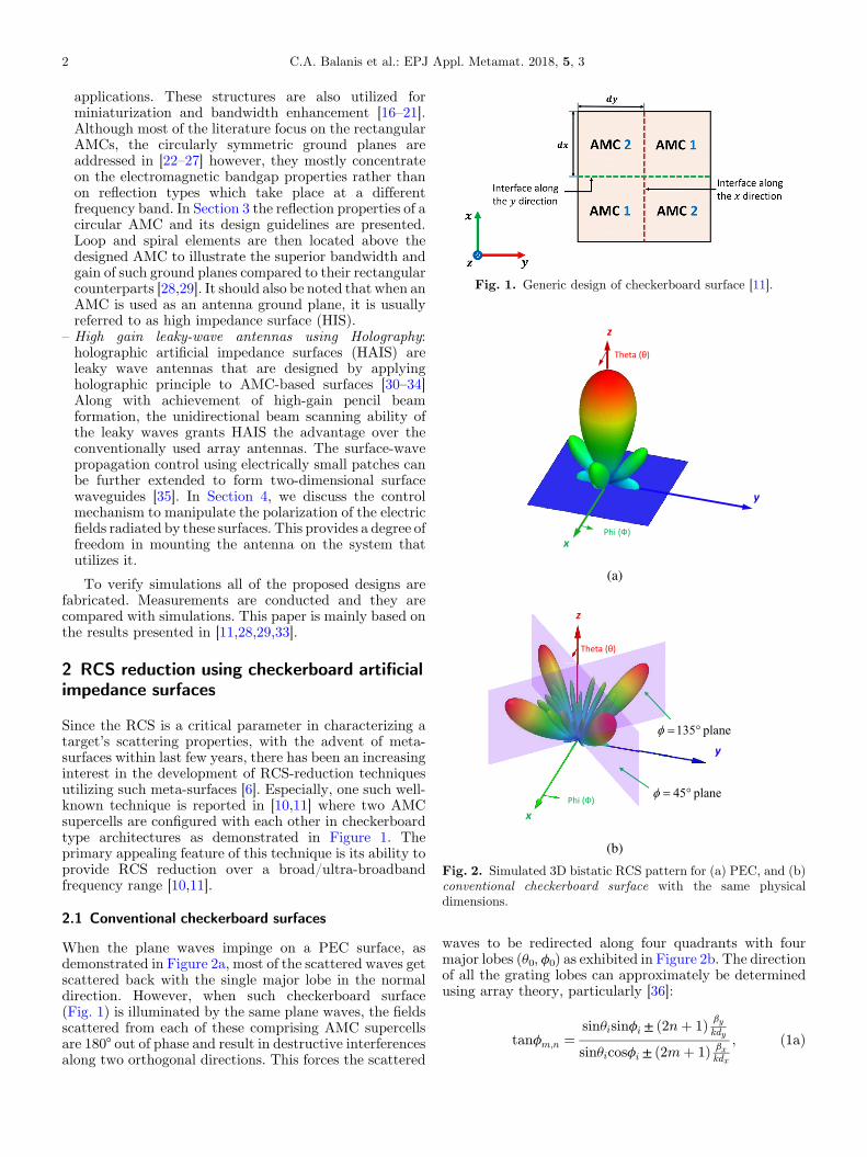
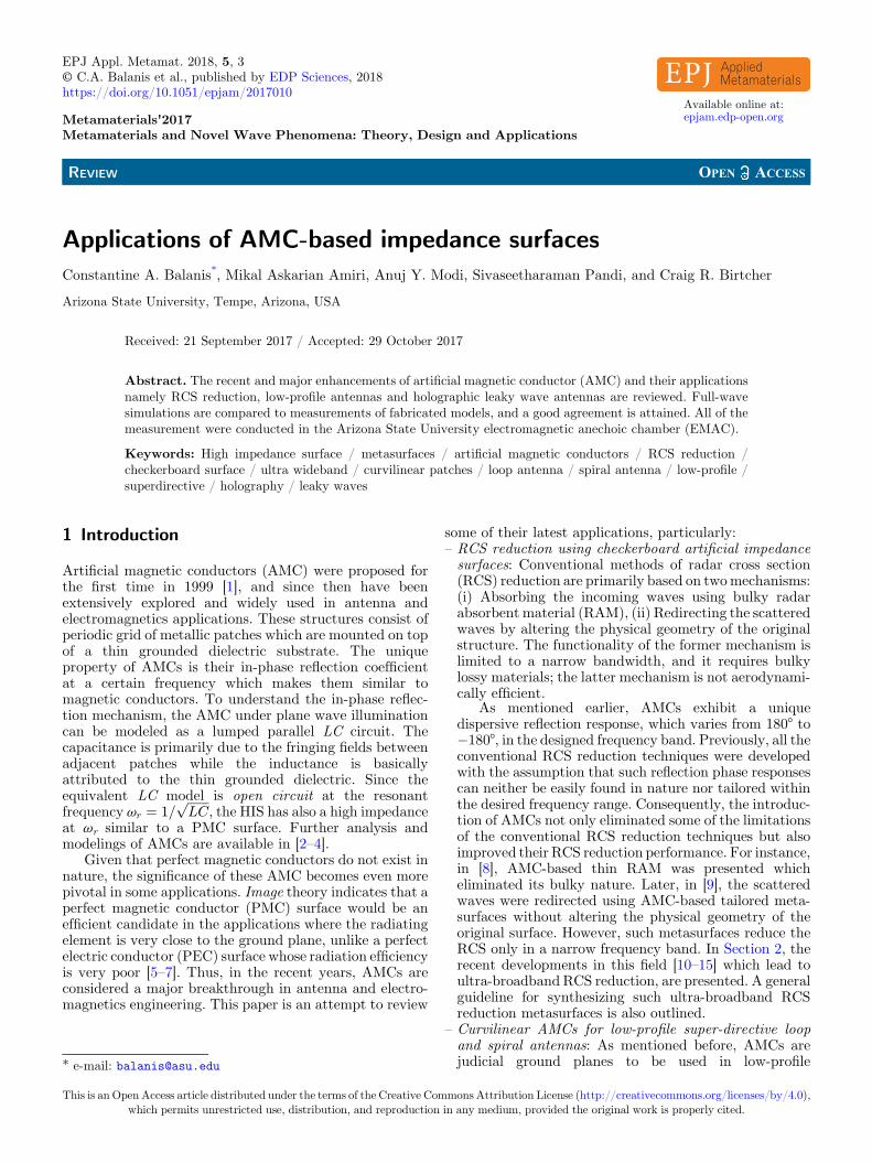
Fig. 1. Generic design of checkerboard surface [11].
2 C.A. Balanis et al.: EPJ Appl. Metamat. 2018, 5, 3
applications. These structures are also utilized forminiaturization and bandwidth enhancement [16–21].Although most of the literature focus on the rectangularAMCs, the circularly symmetric ground planes areaddressed in [22–27] however, they mostly concentrateon the electromagnetic bandgap properties rather thanon reflection types which take place at a differentfrequency band. In Section 3 the reflection properties of acircular AMC and its design guidelines are presented.Loop and spiral elements are then located above thedesigned AMC to illustrate the superior bandwidth andgain of such ground planes compared to their rectangularcounterparts [28,29]. It should also be noted that when anAMC is used as an antenna ground plane, it is usuallyreferred to as high impedance surface (HIS).
–
Fig. 2. Simulated 3D bistatic RCS pattern for (a) PEC, and (b)conventional checkerboard surface with the same physicaldimensions.
High gain leaky-wave antennas using Holography:holographic artificial impedance surfaces (HAIS) areleaky wave antennas that are designed by applyingholographic principle to AMC-based surfaces [30–34]Along with achievement of high-gain pencil beamformation, the unidirectional beam scanning ability ofthe leaky waves grants HAIS the advantage over theconventionally used array antennas. The surface-wavepropagation control using electrically small patches canbe further extended to form two-dimensional surfacewaveguides [35]. In Section 4, we discuss the controlmechanism to manipulate the polarization of the electricfields radiated by these surfaces. This provides a degree offreedom in mounting the antenna on the system thatutilizes it.
To verify simulations all of the proposed designs arefabricated. Measurements are conducted and they arecompared with simulations. This paper is mainly based onthe results presented in [11,28,29,33].
2 RCS reduction using checkerboard artificialimpedance surfaces
Since the RCS is a critical parameter in characterizing atarget’s scattering properties, with the advent of meta-surfaces within last few years, there has been an increasinginterest in the development of RCS-reduction techniquesutilizing such meta-surfaces [6]. Especially, one such well-known technique is reported in [10,11] where two AMCsupercells are configured with each other in checkerboardtype architectures as demonstrated in Figure 1. Theprimary appealing feature of this technique is its ability toprovide RCS reduction over a broad/ultra-broadbandfrequency range [10,11].
2.1 Conventional checkerboard surfaces
When the plane waves impinge on a PEC surface, asdemonstrated in Figure 2a, most of the scattered waves getscattered back with the single major lobe in the normaldirection. However, when such checkerboard surface(Fig. 1) is illuminated by the same plane waves, the fieldsscattered from each of these comprising AMC supercellsare 180° out of phase and result in destructive interferencesalong two orthogonal directions. This forces the scattered
waves to be redirected along four quadrants with fourmajor lobes (u0, f0) as exhibited in Figure 2b. The directionof all the grating lobes can approximately be determinedusing array theory, particularly [36]:
tanfm;n ¼sinuisinfi ± ð2nþ 1Þ by
kdy
sinuicosfi ± ð2mþ 1Þ bxkdx
; ð1aÞ
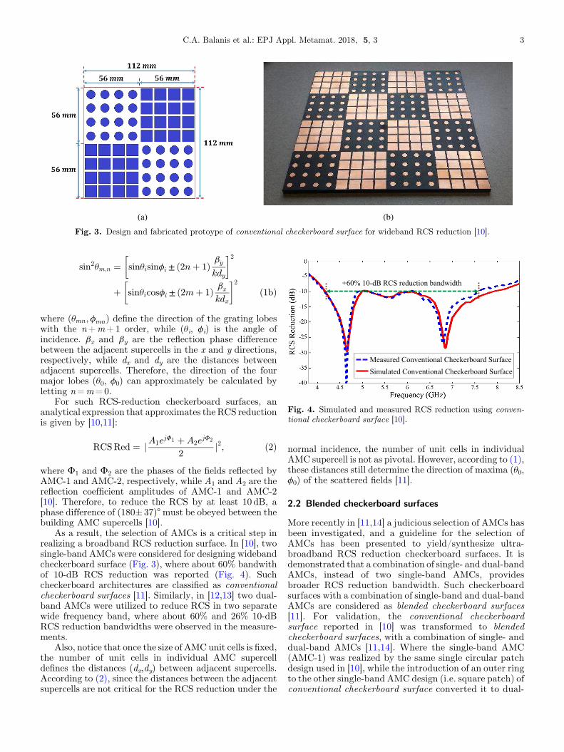
Fig. 3. Design and fabricated protoype of conventional checkerboard surface for wideband RCS reduction [10].
Fig. 4. Simulated and measured RCS reduction using conven-tional checkerboard surface [10].
C.A. Balanis et al.: EPJ Appl. Metamat. 2018, 5, 3 3
sin2um;n ¼ sinuisinfi ± ð2nþ 1Þ by
kdy
� �2
þ sinuicosfi ± ð2mþ 1Þ bx
kdx
� �2ð1bÞ
where (umn;fmn) define the direction of the grating lobeswith the n+m+1 order, while (ui, fi) is the angle ofincidence. bx and by are the reflection phase differencebetween the adjacent supercells in the x and y directions,respectively, while dx and dy are the distances betweenadjacent supercells. Therefore, the direction of the fourmajor lobes (u0, f0) can approximately be calculated byletting n=m=0.
For such RCS-reduction checkerboard surfaces, ananalytical expression that approximates the RCS reductionis given by [10,11]:
RCSRed ¼ jA1ejF1 þ A2e
jF2
2j2; ð2Þ
where F1 and F2 are the phases of the fields reflected byAMC-1 and AMC-2, respectively, while A1 and A2 are thereflection coefficient amplitudes of AMC-1 and AMC-2[10]. Therefore, to reduce the RCS by at least 10 dB, aphase difference of (180±37)°must be obeyed between thebuilding AMC supercells [10].
As a result, the selection of AMCs is a critical step inrealizing a broadband RCS reduction surface. In [10], twosingle-band AMCs were considered for designing widebandcheckerboard surface (Fig. 3), where about 60% bandwithof 10-dB RCS reduction was reported (Fig. 4). Suchcheckerboard architectures are classified as conventionalcheckerboard surfaces [11]. Similarly, in [12,13] two dual-band AMCs were utilized to reduce RCS in two separatewide frequency band, where about 60% and 26% 10-dBRCS reduction bandwidths were observed in the measure-ments.
Also, notice that once the size of AMC unit cells is fixed,the number of unit cells in individual AMC supercelldefines the distances (dx,dy) between adjacent supercells.According to (2), since the distances between the adjacentsupercells are not critical for the RCS reduction under the
normal incidence, the number of unit cells in individualAMC supercell is not as pivotal. However, according to (1),these distances still determine the direction of maxima (u0,f0) of the scattered fields [11].
2.2 Blended checkerboard surfaces
More recently in [11,14] a judicious selection of AMCs hasbeen investigated, and a guideline for the selection ofAMCs has been presented to yield/synthesize ultra-broadband RCS reduction checkerboard surfaces. It isdemonstrated that a combination of single- and dual-bandAMCs, instead of two single-band AMCs, providesbroader RCS reduction bandwidth. Such checkerboardsurfaces with a combination of single-band and dual-bandAMCs are considered as blended checkerboard surfaces[11]. For validation, the conventional checkerboardsurface reported in [10] was transformed to blendedcheckerboard surfaces, with a combination of single- anddual-band AMCs [11,14]. Where the single-band AMC(AMC-1) was realized by the same single circular patchdesign used in [10], while the introduction of an outer ringto the other single-band AMC design (i.e. square patch) ofconventional checkerboard surface converted it to dual-
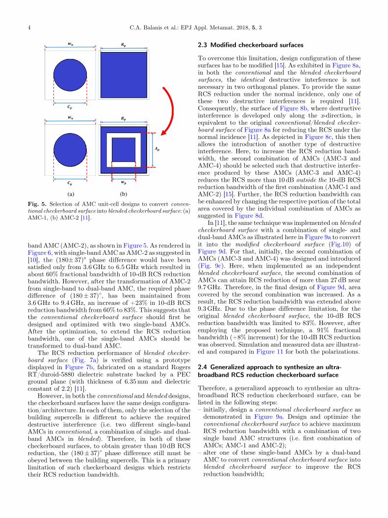
Fig. 5. Selection of AMC unit-cell designs to convert conven-tional checkerboard surface into blended checkerboard surface: (a)AMC-1, (b) AMC-2 [11].
4 C.A. Balanis et al.: EPJ Appl. Metamat. 2018, 5, 3
band AMC (AMC-2), as shown in Figure 5. As rendered inFigure 6, with single-band AMC as AMC-2 as suggested in[10], the (180± 37)° phase difference would have beensatisfied only from 3.6GHz to 6.5GHz which resulted inabout 60% fractional bandwidth of 10-dB RCS reductionbandwidth. However, after the transformation of AMC-2from single-band to dual-band AMC, the required phasedifference of (180± 37)�, has been maintained from3.6GHz to 9.4GHz, an increase of +23% in 10-dB RCSreduction bandwidth from 60% to 83%. This suggests thatthe conventional checkerboard surface should first bedesigned and optimized with two single-band AMCs.After the optimization, to extend the RCS reductionbandwidth, one of the single-band AMCs should betransformed to dual-band AMC.
The RCS reduction performance of blended checker-board surface (Fig. 7a) is verified using a prototypedisplayed in Figure 7b, fabricated on a standard RogersRT/duroid-5880 dielectric substrate backed by a PECground plane (with thickness of 6.35mm and dielectricconstant of 2.2) [11].
However, in both the conventional and blended designs,the checkerboard surfaces have the same design configura-tion/architecture. In each of them, only the selection of thebuilding supercells is different to achieve the requireddestructive interference (i.e. two different single-bandAMCs in conventional, a combination of single- and dual-band AMCs in blended). Therefore, in both of thesecheckerboard surfaces, to obtain greater than 10 dB RCSreduction, the (180±37)� phase difference still must beobeyed between the building supercells. This is a primarylimitation of such checkerboard designs which restrictstheir RCS reduction bandwidth.
2.3 Modified checkerboard surfaces
To overcome this limitation, design configuration of thesesurfaces has to be modified [15]. As exhibited in Figure 8a,in both the conventional and the blended checkerboardsurfaces, the identical destructive interference is notnecessary in two orthogonal planes. To provide the sameRCS reduction under the normal incidence, only one ofthese two destructive interferences is required [11].Consequently, the surface of Figure 8b, where destructiveinterference is developed only along the x-direction, isequivalent to the original conventional/blended checker-board surface of Figure 8a for reducing the RCS under thenormal incidence [11]. As depicted in Figure 8c, this thenallows the introduction of another type of destructiveinterference. Here, to increase the RCS reduction band-width, the second combination of AMCs (AMC-3 andAMC-4) should be selected such that destructive interfer-ence produced by these AMCs (AMC-3 and AMC-4)reduces the RCS more than 10 dB outside the 10-dB RCSreduction bandwidth of the first combination (AMC-1 andAMC-2) [15]. Further, the RCS reduction bandwidth canbe enhanced by changing the respective portion of the totalarea covered by the individual combination of AMCs assuggested in Figure 8d.
In [11], the same technique was implemented on blendedcheckerboard surface with a combination of single- anddual-band AMCs as illustrated here in Figure 9a to convertit into the modified checkerboard surface (Fig.10) ofFigure 9d. For that, initially, the second combination ofAMCs (AMC-3 and AMC-4) was designed and introduced(Fig. 9c). Here, when implemented as an independentblended checkerboard surface, the second combination ofAMCs can attain RCS reduction of more than 27 dB near9.7GHz. Therefore, in the final design of Figure 9d, areacovered by the second combination was increased. As aresult, the RCS reduction bandwidth was extended above9.3GHz. Due to the phase difference limitation, for theoriginal blended checkerboard surface, the 10-dB RCSreduction bandwidth was limited to 83%. However, afteremploying the proposed technique, a 91% fractionalbandwidth (+8% increment) for the 10-dB RCS reductionwas observed. Simulation and measured data are illustrat-ed and compared in Figure 11 for both the polarizations.
2.4 Generalized approach to synthesize an ultra-broadband RCS reduction checkerboard surface
Therefore, a generalized approach to synthesize an ultra-broadband RCS reduction checkerboard surface, can belisted in the following steps:
– initially, design a conventional checkerboard surface asdemonstrated in Figure 9a. Design and optimize theconventional checkerboard surface to achieve maximumRCS reduction bandwidth with a combination of twosingle band AMC structures (i.e. first combination ofAMCs; AMC-1 and AMC-2);–
alter one of these single-band AMCs by a dual-bandAMC to convert conventional checkerboard surface intoblended checkerboard surface to improve the RCSreduction bandwidth;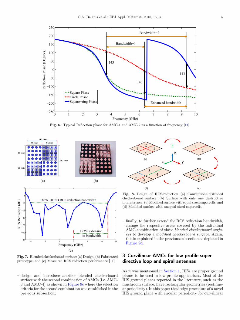
Fig. 7. Blended checkerboard surface: (a) Design, (b) Fabricatedprototype, and (c) Measured RCS reduction performance [11].
Fig. 8. Design of RCS-reduction (a) Conventional/Blendedcheckerboard surface, (b) Surface with only one destructiveintereference, (c)Modified surface with equal sized supercells, and(d) Modified surface with unequal sized supercells.
Fig. 6. Typical Reflection phase for AMC-1 and AMC-2 as a function of frequency [11].
C.A. Balanis et al.: EPJ Appl. Metamat. 2018, 5, 3 5
–
design and introduce another blended checkerboardsurface with the second combination of AMCs (i.e. AMC-3 and AMC-4) as shown in Figure 9c where the selectioncriteria for the second combination was established in theprevious subsection;–
finally, to further extend the RCS reduction bandwidth,change the respective areas covered by the individualAMC-combination of these blended checkerboard surfa-ces to develop a modified checkerboard surface. Again,this is explained in the previous subsection as depicted inFigure 9d.3 Curvilinear AMCs for low-profile super-directive loop and spiral antennas
As it was mentioned in Section 1, HISs are proper groundplanes to be used in low-profile applications. Most of theHIS ground planes reported in the literature, such as themushroom surface, have rectangular geometries (rectiline-ar periodicity). In this paper the design procedure of a novelHIS ground plane with circular periodicity for curvilinear
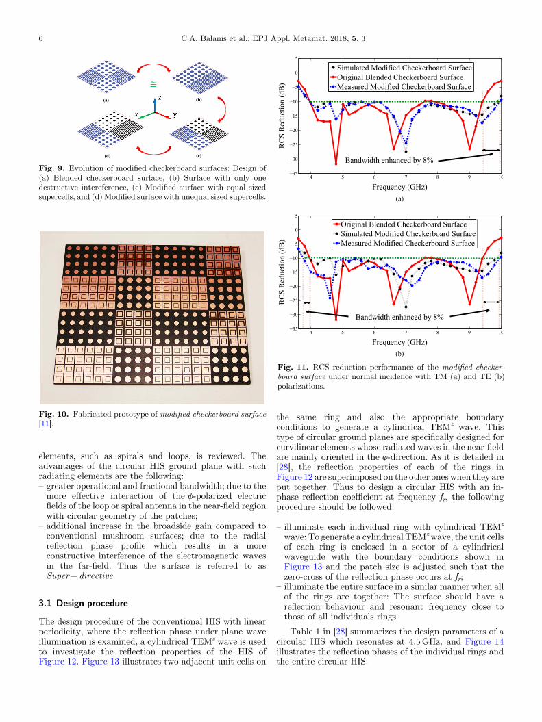
Fig. 9. Evolution of modified checkerboard surfaces: Design of(a) Blended checkerboard surface, (b) Surface with only onedestructive intereference, (c) Modified surface with equal sizedsupercells, and (d) Modified surface with unequal sized supercells.
Fig. 10. Fabricated prototype of modified checkerboard surface[11].
Fig. 11. RCS reduction performance of the modified checker-board surface under normal incidence with TM (a) and TE (b)polarizations.
6 C.A. Balanis et al.: EPJ Appl. Metamat. 2018, 5, 3
elements, such as spirals and loops, is reviewed. Theadvantages of the circular HIS ground plane with suchradiating elements are the following:
– greater operational and fractional bandwidth; due to themore effective interaction of the f-polarized electricfields of the loop or spiral antenna in the near-field regionwith circular geometry of the patches;–
additional increase in the broadside gain compared toconventional mushroom surfaces; due to the radialreflection phase profile which results in a moreconstructive interference of the electromagnetic wavesin the far-field. Thus the surface is referred to asSuper� directive.3.1 Design procedure
The design procedure of the conventional HIS with linearperiodicity, where the reflection phase under plane waveillumination is examined, a cylindrical TEMz wave is usedto investigate the reflection properties of the HIS ofFigure 12. Figure 13 illustrates two adjacent unit cells on
the same ring and also the appropriate boundaryconditions to generate a cylindrical TEMz wave. Thistype of circular ground planes are specifically designed forcurvilinear elements whose radiated waves in the near-fieldare mainly oriented in the ’-direction. As it is detailed in[28], the reflection properties of each of the rings inFigure 12 are superimposed on the other ones when they areput together. Thus to design a circular HIS with an in-phase reflection coefficient at frequency fr, the followingprocedure should be followed:
–
illuminate each individual ring with cylindrical TEMzwave: To generate a cylindrical TEMzwave, the unit cellsof each ring is enclosed in a sector of a cylindricalwaveguide with the boundary conditions shown inFigure 13 and the patch size is adjusted such that thezero-cross of the reflection phase occurs at fr;
–
illuminate the entire surface in a similar manner when allof the rings are together: The surface should have areflection behaviour and resonant frequency close tothose of all individuals rings.Table 1 in [28] summarizes the design parameters of acircular HIS which resonates at 4.5GHz, and Figure 14illustrates the reflection phases of the individual rings andthe entire circular HIS.
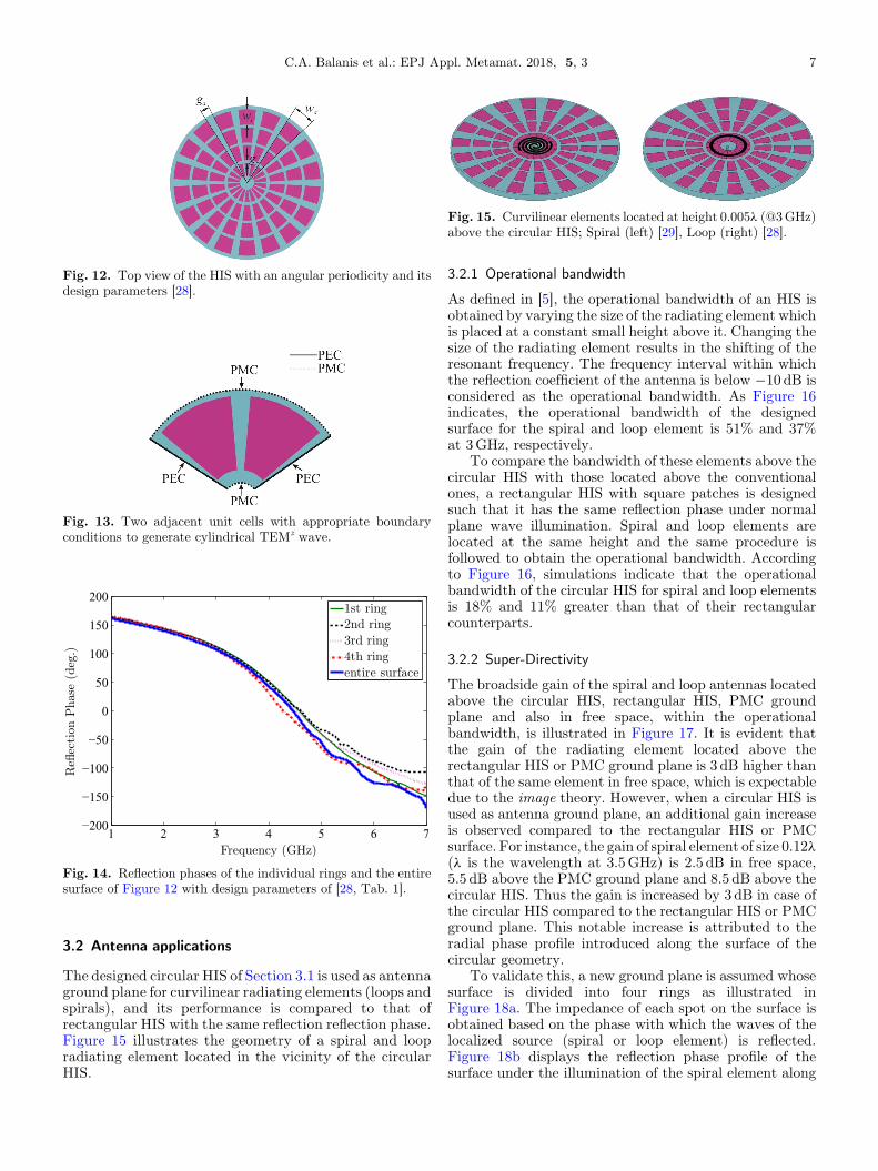
Fig. 12. Top view of the HIS with an angular periodicity and itsdesign parameters [28].
Fig. 13. Two adjacent unit cells with appropriate boundaryconditions to generate cylindrical TEMz wave.
Fig. 14. Reflection phases of the individual rings and the entiresurface of Figure 12 with design parameters of [28, Tab. 1].
Fig. 15. Curvilinear elements located at height 0.005l (@3GHz)above the circular HIS; Spiral (left) [29], Loop (right) [28].
C.A. Balanis et al.: EPJ Appl. Metamat. 2018, 5, 3 7
3.2 Antenna applications
The designed circular HIS of Section 3.1 is used as antennaground plane for curvilinear radiating elements (loops andspirals), and its performance is compared to that ofrectangular HIS with the same reflection reflection phase.Figure 15 illustrates the geometry of a spiral and loopradiating element located in the vicinity of the circularHIS.
3.2.1 Operational bandwidth
As defined in [5], the operational bandwidth of an HIS isobtained by varying the size of the radiating element whichis placed at a constant small height above it. Changing thesize of the radiating element results in the shifting of theresonant frequency. The frequency interval within whichthe reflection coefficient of the antenna is below �10 dB isconsidered as the operational bandwidth. As Figure 16indicates, the operational bandwidth of the designedsurface for the spiral and loop element is 51% and 37%at 3GHz, respectively.
To compare the bandwidth of these elements above thecircular HIS with those located above the conventionalones, a rectangular HIS with square patches is designedsuch that it has the same reflection phase under normalplane wave illumination. Spiral and loop elements arelocated at the same height and the same procedure isfollowed to obtain the operational bandwidth. Accordingto Figure 16, simulations indicate that the operationalbandwidth of the circular HIS for spiral and loop elementsis 18% and 11% greater than that of their rectangularcounterparts.
3.2.2 Super-Directivity
The broadside gain of the spiral and loop antennas locatedabove the circular HIS, rectangular HIS, PMC groundplane and also in free space, within the operationalbandwidth, is illustrated in Figure 17. It is evident thatthe gain of the radiating element located above therectangular HIS or PMC ground plane is 3 dB higher thanthat of the same element in free space, which is expectabledue to the image theory. However, when a circular HIS isused as antenna ground plane, an additional gain increaseis observed compared to the rectangular HIS or PMCsurface. For instance, the gain of spiral element of size 0.12l(l is the wavelength at 3.5GHz) is 2.5 dB in free space,5.5 dB above the PMC ground plane and 8.5 dB above thecircular HIS. Thus the gain is increased by 3 dB in case ofthe circular HIS compared to the rectangular HIS or PMCground plane. This notable increase is attributed to theradial phase profile introduced along the surface of thecircular geometry.
To validate this, a new ground plane is assumed whosesurface is divided into four rings as illustrated inFigure 18a. The impedance of each spot on the surface isobtained based on the phase with which the waves of thelocalized source (spiral or loop element) is reflected.Figure 18b displays the reflection phase profile of thesurface under the illumination of the spiral element along
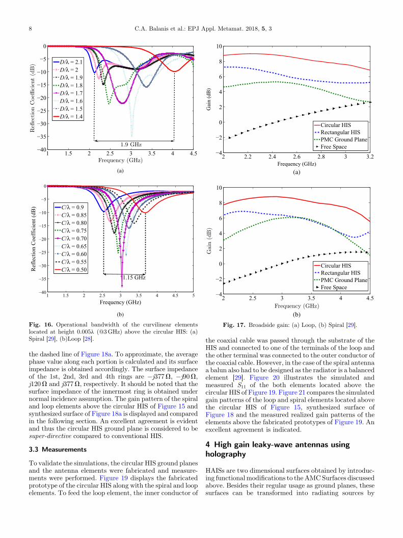
Fig. 16. Operational bandwidth of the curvilinear elementslocated at height 0.005l (@3GHz) above the circular HIS: (a)Spiral [29], (b)Loop [28].
Fig. 17. Broadside gain: (a) Loop, (b) Spiral [29].
8 C.A. Balanis et al.: EPJ Appl. Metamat. 2018, 5, 3
the dashed line of Figure 18a. To approximate, the averagephase value along each portion is calculated and its surfaceimpedance is obtained accordingly. The surface impedanceof the 1st, 2nd, 3rd and 4th rings are �j377V, �j90V,j120V and j377V, respectively. It should be noted that thesurface impedance of the innermost ring is obtained undernormal incidence assumption. The gain pattern of the spiraland loop elements above the circular HIS of Figure 15 andsynthesized surface of Figure 18a is displayed and comparedin the following section. An excellent agreement is evidentand thus the circular HIS ground plane is considered to besuper-directive compared to conventional HIS.
3.3 Measurements
To validate the simulations, the circular HIS ground planesand the antenna elements were fabricated and measure-ments were performed. Figure 19 displays the fabricatedprototype of the circular HIS along with the spiral and loopelements. To feed the loop element, the inner conductor of
the coaxial cable was passed through the substrate of theHIS and connected to one of the terminals of the loop andthe other terminal was connected to the outer conductor ofthe coaxial cable. However, in the case of the spiral antennaa balun also had to be designed as the radiator is a balancedelement [29]. Figure 20 illustrates the simulated andmeasured S11 of the both elements located above thecircular HIS of Figure 19. Figure 21 compares the simulatedgain patterns of the loop and spiral elements located abovethe circular HIS of Figure 15, synthesized surface ofFigure 18 and the measured realized gain patterns of theelements above the fabricated prototypes of Figure 19. Anexcellent agreement is indicated.
4 High gain leaky-wave antennas usingholography
HAISs are two dimensional surfaces obtained by introduc-ing functional modifications to the AMCSurfaces discussedabove. Besides their regular usage as ground planes, thesesurfaces can be transformed into radiating sources by
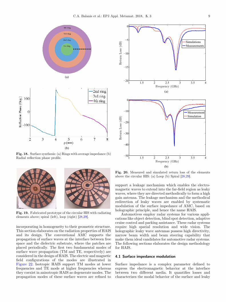
Fig. 18. Surface synthesis: (a) Rings with average impedance (b)Radial reflection phase profile.
Fig. 19. Fabricated prototype of the circular HIS with radiatingelements above; spiral (left), loop (right) [28,29].
Fig. 20. Measured and simulated return loss of the elementsabove the circular HIS: (a) Loop (b) Spiral [28,29].
C.A. Balanis et al.: EPJ Appl. Metamat. 2018, 5, 3 9
incorporating in homogeneity to their geometric structure.This section elaborates on the radiation properties of HAISand its design. The conventional AMC supports thepropagation of surface waves at the interface between freespace and the dielectric substrate, where the patches areplaced periodically. The first two fundamental modes ofsurface wave propagation (TM and TE, respectively) areconsidered in the design of HAIS. The electric andmagneticfield configurations of the modes are illustrated inFigure 22. Isotropic HAIS support TM modes at lowerfrequencies and TE mode at higher frequencies whereasthey coexist in anisotropic HAIS as degenerate modes. Thepropagation modes of these surface waves are refined to
support a leakage mechanism which enables the electro-magnetic waves to extend into the far-field region as leakywaves, where they are directed methodically to form a highgain antenna. The leakage mechanism and the methodicalredirection of leaky waves are enabled by systematicmodulation of the surface impedance of AMC, based onholographic principle, and hence the name HAIS.
Automotives employ radar systems for various appli-cations like object detection, blind spot detection, adaptivecruise control and parking assistance. These radar systemsrequire high spatial resolution and wide vision. Theholographic leaky wave antennas possess high directivity,narrow beam width and beam steering capability thatmake them ideal candidates for automotive radar systems.The following sections elaborates the design methodologyfor HAIS.
4.1 Surface impedance modulation
Surface impedance is a complex parameter defined toexpress the electromagnetic behavior at the interfacebetween two different media. It quantifies losses andcharacterizes the modal behavior of the surface and leaky

Fig. 21. Measured and simulated realized gain patterns of theelements above the circular HIS at 2.7GHz: (a) Loop (b) Spiral[28,29].
Fig. 22. Electric and magnetic field configurations of TE andTM modes [33].
Fig. 23. Surface impedance variation with respect to gap sizebetween patches [33].
10 C.A. Balanis et al.: EPJ Appl. Metamat. 2018, 5, 3
waves at the interface [1,6]. Surface impedance of the AMCcan be determined using a 3D electromagnetic simulator orby the transverse resonance method (TRM). Thesemethods are described in [30–35,38–40]. The squaremetallic patches on a dielectric covered ground plane aremodeled as a lumped capacitor connected in parallel to ashorted transmission line whose length is equal to thedielectric substrate thickness. The previous sections
discussed the surface impedance variation of AMC withthe frequency, while this section requires a parametricstudy on the variation of the surface impedance of AMCwith respect to the size of the square patches at a singlefrequency. Figure 23 shows the variation of the surfaceimpedance with respect to size of the square patches for aperiod of 4mm. The surface impedance is a scalar value forisotropic surfaces and a dyad for anisotropic surfaces. Thispaper encompasses only the isotropic surfaces. Hence thesurface impedance values are inductive for TM modes andcapacitive for TE modes of the surface waves.
In order to align the radiation from the leaky waves inone direction to form a highly directive beam, a holographybased surface impedance profile is required. This surfaceimpedance profile is synthesized by varying the patch sizeon the dielectric covered ground plane. The resultingsurface is inhomogeneous with spatial variation of thesurface impedance, which is modulated sinusoidally alongthe direction of propagation of surface waves to engineerthe leakage of electromagnetic energy from the HAIS. Adetailed study on the properties of sinusoidally modulatedimpedance surfaces is presented in [41–45]. Sinusoidalmodulation of the surface impedance is periodic along thedirection of surface wave propagation, which is expressedas
ZsðxÞ ¼ jXa 1þM cos2xp
p
� �� �; ð3Þ
where Xa is the average surface impedance, M is themodulation index, p is the period of modulation.
The periodic variation of surface impedance results inperiodic electric and magnetic fields that exist as Floquetmodes. Although infinite number of Floquet modes exist,only three modes are dominant for sinusoidal surfaceimpedance modulation. These modes are identified basedon their indices. While n=0 remain as a surface waveFloquet mode, n=� 1 and n=1 exist as leaky wavemodes.The n=� 1 mode corresponds to forward leaky waveswhich radiates in the forward direction while n=1 moderadiates in the opposite direction to the direction of

Fig. 24. Forward and backward leaky wave modes.
Fig. 25. Conventional HAIS: (a) Ground plane designed toradiate a pencil beam using square patches (b) Core of HAIS witha monopole to excite surface waves.
C.A. Balanis et al.: EPJ Appl. Metamat. 2018, 5, 3 11
propagation, as shown in Figure 24. The forward andbackward waves are excited by controlling the period of thesinusoidal modulation. The propagation constants of thethree modes are
kn ¼ kþ 2np
pn ¼ 0; ± 1; ð4Þ
where k is the propagation constant of the surface wavemode with index zero and n is the index of the mode.
4.2 HAIS with desired polarizations
An HAIS is designed by realizing a surface impedanceprofile given by the holographic principle and sinusoidalmodulation. This is accomplished by using the interferencepattern of the holographic principle as the argument for thesinusoidal modulation function in (3). The interferencepattern is configured by performing a dot product betweenthe phase projections of the source and desired waves onthe surface of HAIS. The source wave is the surface waveexcited on the HAIS using an electrically small radiatingsource (in this case a monopole) and the desired wave is apencil beam in the desired direction. A conventional HAISis designed to radiate along u=35° in xz plane according to
ZsðxÞ ¼ jXa½1þMReðe�k0xsin35°ejkrÞ�; ð5Þwhere Xa=337V is the average surface reactance, k isphase constant of the surface wave, M=0.5 is themodulation index, k0 is the free-space phase constant,and r is the radial distance from the monopole. Theresultant structure illustrated in Figure 25, and designedfor an operation frequency of 10GHz, is capable of forminga pencil beam in the desired direction that is contributed byboth forward and backward leaky waves. The radiationpattern along the cross sectional plane of the pencil beam isshown in Figure 26. The holographic interference patternprovides the spatial adjustment to the period of thesinusoidal modulation to align the radiations from theforward and backward leaky waves in the same direction atthe design frequency. The frequency band around thedesign frequency, where the forward and backward leakywaves radiate in the same direction is referred to as thephase-crossover frequency band. The HAIS under phase-crossover frequency operation is capable of radiating alinearly polarized electric field along the peak direction ofthe pencil beam. TMmode leaky waves radiate a vertically
polarized electric fields that are oriented normal to thesurface and TE mode leaky waves radiate horizontallypolarized waves that are parallel to HAIS.
A control of the polarization of the radiated electricfields can be accomplished by modifying the holographicpattern and operating at nonphase-crossover frequencyband where the forward and backward leaky waves radiatein different directions. The holographic interferencepattern can be viewed as concentric ellipses sharingcommon center, as displayed in Figure 27. This interferencepattern can be modified to establish a control over thepolarization of the radiated fields. The holographic patternrequired to achieve different polarizations along the pencilbeam, and their corresponding frequency bands of opera-tion are discussed in the following sections.
4.2.1 Horizontal polarization
The concentric ellipses have a plane of symmetry asdemonstrated in Figure 27. HAIS is divided into twosymmtric halves by this plane. A phase shift of 180° isintroduced to one of these symmetric halves relative to theother to obtain a modified HAIS that radiates horizontallypolarized waves along the peak of the pencil beam as shownin Figure 28a. This is due to the reinforcement of the E’
components. The surface is operated at a nonphase-crossover frequency band. The radiation pattern along theplane of symmetry is presented in Figure 28b.
This structure was fabricated using the dielectricsubstrate ROGERS 5880 with a thickness of 0.125 in.The surface dimensions are 9:400 � 7:800. 3600 square
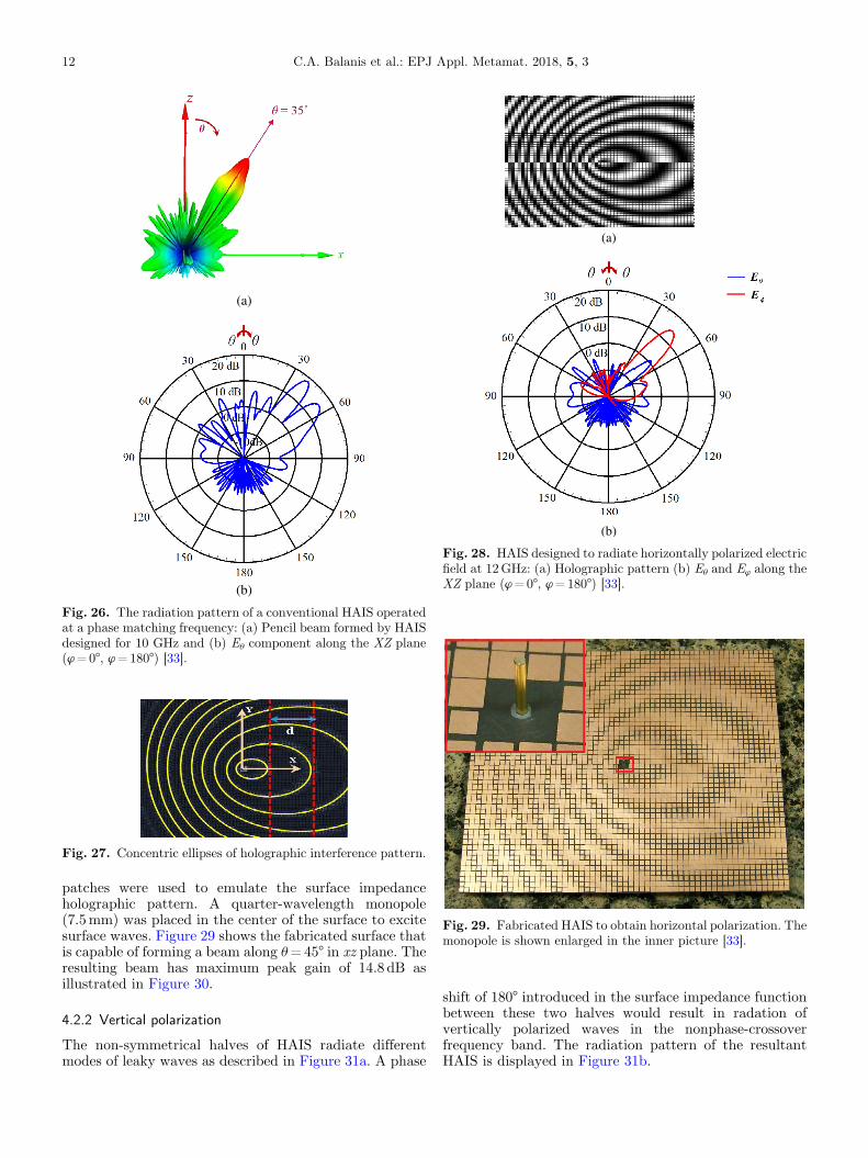
Fig. 26. The radiation pattern of a conventional HAIS operatedat a phase matching frequency: (a) Pencil beam formed by HAISdesigned for 10 GHz and (b) Eu component along the XZ plane(’=0°, ’=180°) [33].
Fig. 27. Concentric ellipses of holographic interference pattern.
Fig. 28. HAIS designed to radiate horizontally polarized electricfield at 12GHz: (a) Holographic pattern (b) Eu and E’ along theXZ plane (’=0°, ’=180°) [33].
Fig. 29. Fabricated HAIS to obtain horizontal polarization. Themonopole is shown enlarged in the inner picture [33].
12 C.A. Balanis et al.: EPJ Appl. Metamat. 2018, 5, 3
patches were used to emulate the surface impedanceholographic pattern. A quarter-wavelength monopole(7.5mm) was placed in the center of the surface to excitesurface waves. Figure 29 shows the fabricated surface thatis capable of forming a beam along u=45° in xz plane. Theresulting beam has maximum peak gain of 14.8 dB asillustrated in Figure 30.
4.2.2 Vertical polarization
The non-symmetrical halves of HAIS radiate differentmodes of leaky waves as described in Figure 31a. A phase
shift of 180° introduced in the surface impedance functionbetween these two halves would result in radation ofvertically polarized waves in the nonphase-crossoverfrequency band. The radiation pattern of the resultantHAIS is displayed in Figure 31b.

Fig. 30. Comparison between measured and simulated E’
components along the XZ plane (’=0°, ’=180°) [33].
Fig. 31. HAIS designed to radiate vertically polarized electricfield at 12GHz: (a) Holographic pattern (b) Eu and E’ along theXZ plane [33].
Fig. 32. HAIS designed to radiate circularly polarized electricfield at 12GHz: (a) Holographic pattern (b) RHCP and LHCPcomponents along the XZ plane [33].
C.A. Balanis et al.: EPJ Appl. Metamat. 2018, 5, 3 13
4.2.3 Circular polarization
Circularly polarized radiated fields can be accomplished bysuperimposing the surface impedance modulation func-tions corresponding to vertical and horizontal polarizationswith a phase shift of 90°. The resulting structure is
illustrated in Figure 32. The sense of rotation of thecircularly polarized fields is determined by the modulationfunction of the component which undergoes the 90° phaseshift. The radiation pattern of the HAIS is illustrated inFigure 32b.
HAISs are two dimensional leaky wave antennas that arecapable of forming a pencil beam in a desired direction. Theyare derived by incorporating inhomogeneity to the surfaceimpedance of the AMC surfaces discussed in the previoussections. The inhomogeneous surface impedance is aradiation mechanism that facilitates the leakage of surfacewaves supported by the AMC surfaces. The radiationpatterns of HAISs indicate the achievement of all the typesof polarizations by varying the holographic pattern of theAMC based structure. The holographic patterns enable thereinforcement of the desired vector components of thesurface waves to leak out of the surface resulting in theradiation of pencil beam with desired polarization.
5 Conclusions
In this paper, some recent applications of AMC-basedsurfaces for RCS reduction, low-profile antenna design andhigh gain leaky-wave antennas were discussed. Theconclusions for each topic can be summarized as follow:
– RCS reduction using checkerboard artificial impedancesurfaces: The advancements in metasurfaces tailored inthe checkerboard type architecture, were reviewed where
14 C.A. Balanis et al.: EPJ Appl. Metamat. 2018, 5, 3
the fundamental mechanism was elaborated withcorresponding governing formulas and simulated RCSpatterns. First, the conventional checkerboard surfaceusing two single-band AMCs was presented whichresulted in 10 dB RCS reduction bandwidth enhance-ment from 27% to 60%. Then, the judicious selectioncriteria for AMCs was discussed which ultimately led toblended checkerboard surfaces which increased the 10 dBRCS reduction bandwidth from 60% to 83%. However,RCS reduction bandwidth of such surfaces were stilllimited by the reflection phase difference criteria of(180±37)°. After that, a review of a technique formodifying such blended checkerboard surfaces waspresented which eliminated this limitation and enhancedthe 10-dB RCS reduction bandwidth from 83% to 91%.A general guideline for synthesizing such ultra-broad-band RCS reduction metasurfaces was outlined.
–
Curvilinear AMCs for low-profile super-directive loopand spiral antennas: The design procedure of a novel HISground plane with circular periodicity was reviewed. Thistype of HISs are specifically designed for curvilinearelements, such as spirals and loops. Simulations indicatedthat the operational bandwidth of the spiral and looplocated above circular HISs are 18% and 11% greaterthan those of the spiral and loop above conventional HISswith rectilinear periodicity. An additional 3 dB increasein the directivity (compared to the PMC and rectangularHIS) was also observed which is attributed to the radialphase profile introduced along the surface.–
High gain leaky-wave antennas using holography: Thedesign methodology of HAIS, radiating a pencil beamwith a desired polarization was discussed. The holo-graphic pattern required to form a pencil beam isimplemented using the surface impedance modulationtechnique. The surface impedance is modulated byvarying the size of metallic square patches embeddedon a dielectric covered ground plane. It is shown thatholographic pattern modification enables a degree offreedom to control the polarization of the radiated fieldsalong the pencil beam.To validate the simulations, all of the prototypes werefabricated and measurements were performed. An excel-lent agreement was observed throughout.
References
1. D. Sievenpiper, High-Impedance Electromagnetic Surfaces,Ph.D. dissertation, (Dept. Elect. Eng., Univ. California, LosAngeles, Los Angeles, CA, USA, 1999).
2. S. Tretyakov, Analytical modeling in applied electromag-netics, (Artech House, Boston, 2003).
3. O. Luukkonen, C. Simovski, G. Granet, G. Goussetis, D.Lioubtchenko, A.V. Risnen, S.A. Tretyakov, Simple andaccurate analytical model of planar grids and high-impedancesurfaces comprising metal strips or patches, IEEE Trans.Antennas Propag. 56, 1624 (2008).
4. R. Rodrigues-Berral, F. Medina, F. Mesa, M.G. Vigueras,Quasi-analytical modeling of transmission/reflection instrips/slit gratings loaded with dielectric slabs, IEEE Trans.Microw Theory Tech. 60, 405 (2012).
5. Y. Fan, Y. Rahmat-Samii, Reflection phase characterizationsof the EBG ground plane for low profile wire antennaapplications,IEEETrans. Antennas Propag. 51, 2691 (2003).
6. C.A. Balanis, Advanced engineering electromagnetics, 2nded, (Wiley, New York, 2012).
7. A. Vallecchi, J.R. De Luis, F. Capolino, F. De Flaviis, Lowprofile fully planar folded dipole antenna on a high impedancesurface, IEEE Trans. Antennas Propag. 60, 51 (2012).
8. N. Engheta, Thin absorbing screens using metamaterialsurfaces, Proc. IEEE Antennas Propag. Soc. Int. Symp. 2,392 (2002).
9. M. Paquay, J.C. Iriarte, I. Ederra, R. Gonzalo, P. de Maagt,Thin AMC structure for radar cross-section reduction, IEEETrans. Antennas Propag. 55, 3630 (2007).
10. W. Chen, C.A. Balanis, C.R. Birtcher, Checkerboard EBGsurfaces for wideband radar cross section reduction, IEEETrans. Antennas Propag. 63, 2636 (2015).
11. A.Y. Modi, C.A. Balanis, C.R. Birtcher, H. Shaman, Noveldesign of ultrabroadband radar cross section reductionsurfaces using artificial magnetic conductors, IEEE Trans.Antennas Propag. 65, 5406 (2017).
12. W. Chen, C.A. Balanis, C.R. Birtcher, Dual wide-bandcheckerboard surfaces for radar cross section reduction, IEEETrans. Antennas Propag. 64, 4133 (2016).
13. W. Chen, C. A. Balanis, C.R. Birtcher, Dual frequency bandRCS reduction using checkerboard surfaces, Proc. of IEEEInt. Symp. Antennas Propag., San Diego, CA, 2017, pp.1913–1914.
14. A.Y. Modi, C.A. Balanis, C. Birtcher, AMC cells forbroadband RCS reduction checkerboard surfaces, Proc. ofIEEE Int. Symp. Antennas Propag., San Diego, CA, 2017,pp. 1911–1912.
15. A.Y. Modi, C.A. Balanis, C. Birtcher, Novel technique forenhancing RCS reduction bandwidth of checkerboardsurfaces, Proc. of IEEE Int. Symp. Antennas Propag., SanDiego, CA, 2017, pp. 1915–1916.
16. M.Z. Azad, M. Ali, Novel wideband directional dipoleantenna on a mushroom like EBG structure, IEEE Trans.Antennas Propag. 56, 1242 (2008).
17. L. Akhoondzadeh-Asl, D.J. Kern, P.S. Hall, D.H. Werner,Wideband dipoles on electromagnetic bandgap groundplanes, IEEE Trans. Antennas Propag. 55, 2426 (2007).
18. H. Mosallaei, K. Sarabandi, Antenna miniaturization andbandwidth enhancement using a reactive impedance sub-strate, IEEE Trans. Antennas Propag. 52, 2403 (2004).
19. D.J. Kern, D.H. Werner, A. Monorchio, L. Lanuzza, M.J.Wilhelm,The design synthesis ofmultiband artificialmagneticconductors using high impedance frequency selective surfaces,IEEE Trans. Antennas Propag. 53, 8 (2005).
20. D.J. Kern, D.H. Werner, A. Monorchio, L. Lanuzza, M.J.Wilhelm, Reconfigurable ultra-thin EBG absorbers usingconducting polymers, Antennas and Propagation SocietyInternational Symposium(APSURSI), 2005 IEEE, 2B, 2005,pp. 204–217.
21. A.C. Durgun, C.A. Balanis C.R. Birtcher, Reflection phasecharacterization of curved high impedance surfaces, IEEETrans. Antennas Propag. 61, 6030 (2013).
22. J. Sarrazin, A.C. Lepage, X. Begaud, Circular high-impedance surfaces characterization, IEEE Lett. AntennasWirel. Propag. 11, 260 (2012).
23. N. Llombart, A. Neto, G. Gerini, Planar circularly symmetricEBG structures for reducing surface waves in printedantennas, IEEE Trans. Antennas Propag. 53, 3210 (2005).

C.A. Balanis et al.: EPJ Appl. Metamat. 2018, 5, 3 15
24. A. Neto, N. Llombart, G. Gerini, P. de Maagt, On theomptimal radiation bandwidth of printed slot antennassurrounded by EBGs, IEEE Trans. Antennas Propag. 54,1074 (2006).
25. M. Ettore, S. Bruni, G. Gerini, A. Neto, N. Llombart, S. Maci,Sector PCS-EG antenna for low-cost high-directivity appli-cations, IEEE Lett. Antennas Wirel. Propag. 6, 537 (2007).
26. M. SalarRahimi, J. Rashed-Mohassel, M. Edalatipour,Radiation properties enhancement of a GSM/WLAN micro-strip antenna using a dual band circularly symmetric EBGsubstrate, IEEE Trans. Antennas Propag. 60, 5491 (2012).
27. T.A. Dendini, Y. Coulibaly, H. Boutayeb, Hybrid dielectricresonator antenna with circular mushroom-like structure forgain improvement, IEEE Trans. Antennas Propag. 57, 1043(2009).
28. M.A. Amiri, C.A. Balanis, C.R. Birtcher, Analysis, designand measurements of circularly symmetric high impedancesurfaces for loop antenna applications, IEEE Trans. Anten-nas Propag. 64, 618 (2015).
29. M.A. Amiri, C.A. Balanis, C.R. Birtcher, Gain andbandwidth enhancement of spiral antenna using circularlysymmetric HIS, IEEE Lett. Antennas Wirel. Propag. 16,1080 (2017).
30. B.H. Fong, J.S. Colburn, J.J. Ottusch, J.L. Visher, D.F.Sievenpiper, Scalar and tensor holographic artificial imped-ance surfaces, IEEE Trans. Antennas Propag. 58, 3212(2010).
31. A.M. Patel, A. Grbic, A printed leaky-wave antenna based ona sinusoidally-modulated reactance surface, IEEE Trans.Antennas Propag. 59, 2087 (2011).
32. S. Maci, G. Minatti, M. Casaletti, M. Bosiljevac, Metasurf-ing: addressing waves on impenetrable metasurfaces, IEEEAntennas Wireless Propag. Lett. 10, 1499 (2011).
33. S. Pandi, C.A. Balanis, C.R. Birtcher, Design of scalarimpedance holographic metasurfaces for antenna beamformation with desired polarization, IEEE Trans. AntennasPropag. 63, 3016 (2015).
34. G. Minatti, S. Maci, P. De Vita, A. Freni, M. Sabbadini, Acircularly-polarized isoflux antenna based on anisotropicmetasurface, IEEE Trans. Antennas Propag. 60, 4998 (2012).
35. R. Quarfoth, D. Sievenpiper, Artificial tensor impedancewave-guides, IEEE Trans. Antennas Propag. 61, 3597(2013).
36. C.A. Balanis, Antenna theory: analysis design, 4th ed.,(Wiley, Hoboken, NJ, USA, 2016).
37. M.A. Amiri, C. Balanis, C. Birtcher, Notable gain enhance-ment of curvilinear elements using a circular HIS groundplane, Proc. of IEEE Int. Symp. Antennas Propag. SanDiego, CA, 2017, pp. 1671–1672.
38. S. Pandi, C.A. Balanis, Antenna beam forming usingholographic artificial impedance surface, Antenna Technol.Appl. Electromagn. (ANTEM), Victoria, BC, 2014, pp. 1–2.
39. O. Luukkonen, C. Simovski, G. Granet, G. Goussetis, D.Lioubtchenko, A.V. Risnen, S.A. Tretyakov, Simple accurateanalytical model of planar grids high-impedance surfacescomprising metal strips patches, IEEE Trans. AntennasPropag. 56, 1624 (2008).
40. A.M. Patel, Controlling electromagnetic surface waves withscalar tensor impedance surfaces, Ph.D. dissertation, (De-partment of Electrical Engineering, The University ofMichigan, Ann Arbor, MI, 2013).
41. A.A. Oliner, A. Hessel, Guided waves on sinusoidally-modulated reactance surfaces, IRE Trans. Antennas Propag.7, 201 (1959).
42. S. Pandi, C.A. Balanis, C.R. Birtcher, Analysis of widebandmultilayered sinusoidally modulated metasurface, IEEEAntennas Wirel. Propag. Lett. 15, 1491 (2016).
43. S. Pandi, C.A. Balanis, C.R. Birtcher, Curvature modeling indesign of circumferentially modulated cylindrical metasur-face LWA, IEEE Antennas Wirel. Propag. Lett. 16, 1024(2016).
44. S. Pandi, S. Ramalingam, C.A. Balanis, C.R. Birtcher,Bandwidth analysis of phase crossover non-phase crossoverfrequency operations of HAIS, IEEE Antennas and Propa-gation International Symposium, San Diego, CA, 2017, pp.287–288.
45. S. Ramalingam, S. Pandi, C.A. Balanis, C.R. Birtcher, Axialand circumferential modulation of cylindrical metasurfaces,2017 IEEE Antennas and Propagation International Sym-posium, San Diego, CA, 2017, pp. 279–280.
Cite this article as: Constantine A. Balanis, Mikal Askarian Amiri , Anuj Y. Modi, Sivaseetharaman Pandi, Craig R. Birtcher ,Applications of AMC-based impedance surfaces, EPJ Appl. Metamat. 2018, 5, 3