Embed Size (px)
Citation preview
Application of double patterning technology to fabricate optical elements:Process simulation, fabrication, and measurementS. Babin, G. Glushenko, T. Weber, T. Kaesebier, E.-B. Kley et al. Citation: J. Vac. Sci. Technol. B 30, 031605 (2012); doi: 10.1116/1.3698315 View online: http://dx.doi.org/10.1116/1.3698315 View Table of Contents: http://avspublications.org/resource/1/JVTBD9/v30/i3 Published by the AVS: Science & Technology of Materials, Interfaces, and Processing Related ArticlesHigh-resolution nondestructive patterning of isolated organic semiconductors J. Vac. Sci. Technol. B 30, 06FB04 (2012) Dual applications of free-standing holographic nanopatterns for lift-off and stencil lithography J. Vac. Sci. Technol. B 30, 06FF04 (2012) High resolution patterning on nonplanar substrates with large height variation using electron beam lithography J. Vac. Sci. Technol. B 30, 06F303 (2012) Fast and continuous patterning on the surface of plastic fiber by using thermal roller imprint J. Vac. Sci. Technol. B 30, 06FB01 (2012) Creating nanoscale Ag patterns on the Si(111)–(√3×√3)R30°-Ag surface via guided self-assembly J. Vac. Sci. Technol. B 30, 050601 (2012) Additional information on J. Vac. Sci. Technol. BJournal Homepage: http://avspublications.org/jvstb Journal Information: http://avspublications.org/jvstb/about/about_the_journal Top downloads: http://avspublications.org/jvstb/top_20_most_downloaded Information for Authors: http://avspublications.org/jvstb/authors/information_for_contributors
Downloaded 10 Oct 2012 to 192.108.69.177. Redistribution subject to AVS license or copyright; see http://avspublications.org/jvstb/about/rights_and_permissions
Application of double patterning technology to fabricate optical elements:Process simulation, fabrication, and measurement
S. Babina) and G. GlushenkoAbeam Technologies, Inc., 5286 Dunnigan Ct., Castro Valley, California 94546
T. Weber, T. Kaesebier and E.-B. KleyFriedrich-Schiller-University Jena, Institute of Applied Physics, Albert-Einstein-Straße 15,D-07743, Jena, Germany
A. SzeghalmiMax Planck Institute of Microstructure Physics, Weinberg 2, Halle (Saale) D-06120, Germany
(Received 12 July 2011; accepted 12 March 2012; published 3 April 2012)
Double patterning is an important technique for the improvement of spatial resolution in fabricated
micro and nanostructures. In this paper, we investigated and applied the double patterning
technique to fabricate diffractive optical elements. Simulations of multiple dry etch and film
deposition steps were performed to study and optimize the vertical profiles of the fabricated
patterns. Etch and deposition characteristics were varied to study their impact on the resulting
vertical profile of the metal layers. The influence of the linewidth of the initial resist pattern and
the process-induced tapering of the grating tops on the optical performance were investigated
in particular. A variably shaped electron-beam lithography system was used for the fabrication of
the initial resist pattern. The spatial frequency was then doubled by means of double patterning.
Broadband aluminum and iridium wire grid polarizers were fabricated for applications down to the
UV range with a feature size of 30 nm, a period of 100 nm, and a vertical aspect ratio of about 5:1.
Optical measurements have confirmed the designed optical properties. VC 2012 American VacuumSociety. [http://dx.doi.org/10.1116/1.3698315]
I. INTRODUCTION
Double patterning is an important technique for the
improvement of spatial resolution in fabricated patterns.
Furthermore, it is an attractive way to fabricate patterns at
resolutions far beyond the limits of traditional optical lithog-
raphy. The principle of double patterning was demonstrated
in 1983.1 Recent progress has led to its application in micro-
electronic manufacturing, and the technique is being adopted
by major semiconductor companies for the volume production
of semiconductor devices.2–5 Among multiple variations of
the double patterning technique, the technology based on the
fabrication of a spacer by conformal deposition of a material,
followed by anisotropic etch of this material, is of high inter-
est. The process is also called spacer patterning technology or
self-aligned double patterning.6 This method is also attractive
for the fabrication of diffractive optical elements, where the
topological elements are mostly repetitive.
In the fabrication process, there are two competing
requirements for a large area of the optical element: high
writing speed and high resolution. Electron-beam lithogra-
phy (EBL) can normally provide either high resolution with
slow writing speed, or can write a large area with high speed
at modest resolution. The double patterning technique per-
fectly suits these two contravening requirements, thereby
extending the manufacturing capabilities of EBL. In semi-
conductor manufacturing, the spacer technique is used to
make a hard mask for ensuing manufacturing processes. In
optical elements, these properly fabricated spacers could
work as wire grid polarizers. They consist of a parallel
arrangement of conductive wires and are characterized by a
high transmission of TM-polarized light, and a suppression
of TE-polarized light.7 A further characteristic is the extinc-
tion ratio defined by the ratio of TM- and TE-polarized light.
In this paper, we investigate the suitability of the double
patterning process for the fabrication of wire grid polarizers.
The investigation is carried out by analyzing the influence of
the fabrication-based deviations from a perfect binary gra-
ting profile on the optical properties of wire grid polarizers.
The TRAVIT software package was used to simulate the com-
plex multistep fabrication process with several deposition
and etching steps, based on an analytical model of dry etch.8
The simulation predicts etch profile, linewidth, variation of
critical dimensions (CD), and placement errors in double
patterning. TRAVIT has been successfully applied to simu-
lations of 22 nm and 11 nm half-pitch designs. Simulations
of the process should complement time-consuming experi-
ments so as to reduce costs and shorten development time.
The influence of linewidth variation of the initial resist pat-
tern and the shape of the tapered grating tops on the grating
optical properties were investigated. To determine the effect
of these deviations from the ideal binary grating profile, the-
oretical calculations using the software GRATING SOLVER9 and
measurements of the optical performance of fabricated sam-
ples were performed. Using a multistep process, including
ultrafast electron-beam lithography and different etching and
deposition techniques, aluminum and iridium gratings with a
period of 100 nm and a vertical aspect ratio of about 5:1a)Electronic mail: [email protected]
031605-1 J. Vac. Sci. Technol. B 30(3), May/Jun 2012 2166-2746/2012/30(3)/031605/5/$30.00 VC 2012 American Vacuum Society 031605-1
Downloaded 10 Oct 2012 to 192.108.69.177. Redistribution subject to AVS license or copyright; see http://avspublications.org/jvstb/about/rights_and_permissions
were fabricated. The fabricated optical elements work as
broadband wire grid polarizers from the infrared to the ultra-
violet spectral region.
II. MODELING
First demonstration of the double patterning process for
the fabrication of wire grid polarizers was shown by the
authors in previous works.10,11 However, the effects of the
double patterning process on the device’s optical properties
have not been discussed. A better understanding of the evo-
lution of the grating structure during fabrication can lead to
an optimization of the grating profile and an enhancement of
the optical properties of the polarizer. Simulating the dry
etch process is a complex problem that requires detailed
knowledge of plasma physics, the interaction of plasmas
with solids, plasma chemistry, kinetics, etc.12–15 Because of
the complexity of this task, it is impractical to expect any
simulation software to be universally applicable to all dry
etch situations. On the other hand, addressing the problem
for specific cases using defined boundary conditions with
given tolerances is feasible and cost effective, and can
deliver usable information.
TRAVIT simulation software, presented by the authors in an
earlier publication,16 uses an analytical model of dry etch.
The software tool is focused on the simulation of the dynam-
ics of etched profiles. In addition, it is capable of calculating
CDs and CD variations resulting from dry etch; these are not
addressed by currently known models.16 The software can
model complex processes involving the combination of dry
etch, film deposition, and electroplating. Furthermore, the
software predicts the etch profile, linewidth, variation of crit-
ical dimensions (CD), and placement errors in double
patterning.
The geometry of the diffractive optical element (DOE) is
defined by the optical design and simulation. This geometry
is the final target of the fabrication process. Double pattern-
ing involves multiple processing steps; each of them has
many parameters. Optimization of this process to achieve
the required geometry can be done experimentally. How-
ever, because of the multidimensional space of parameters
involved, such work is costly and time consuming. Process
simulations can guide the fabrication process and set up tar-
gets for each separate process step; for example, the shape of
the resist profile after development or the thickness of the
spacer layer in the deposition process. Once the target
requirements for each specific process step are known, it is
much easier to develop the double patterning process as
compared to its development when only the final desired ge-
ometry is known.
The vertical resist profile and its thickness after EBL and
resist development were the input parameters for the simula-
tion; they were varied in order to study their effects on the
final shape of the grating. The resist trim process was also
varied in order to optimize the full process. For a specific
resist profile, etch and deposition characteristics were varied
to study their impact on the resulting vertical profile of the
metal layers. The simulations involved are setup of a GDSII
resist pattern, assigning material thicknesses and resist pro-
file after development; resist trim; conformal deposition of
sacrificial layer; anisotropic etch of the sacrificial layer; and
etch of the resist. Each process step includes many variables.
Simulations were repeated with variations of the process pa-
rameters in order to obtain the desired linewidth and vertical
profiles of the metal gratings after the final fabrication step.
When the simulations yielded the desired geometry of the
final grating, the pattern geometries at each intermediate
processing step were used as targets in the respective steps
of the actual fabrication process.
III. EXPERIMENT
The double patterning technique was used to fabricate
high-aspect-ratio metal gratings with a pitch of 100 nm.
First, a multilayered resist was deposited on a fused silica
substrate. The multilayers involved a tempered resist,
chrome, and an e-beam resist. The 200 nm pitch pattern was
written in the resist using a Vistec SB 350 OS electron-beam
lithography system. A lattice aperture was used for the ultra-
fast writing of a high-frequency pattern. The lattice aperture
is located in the electron column and allows for the writing
of a defined character with a single shot; for example, a gra-
ting pattern. Here, the area of the grating determines the
writing time in the system, but the pitch of the grating does
not.17 When using the ZEP 520 resist of Nippon Zeon
Corporation, the writing speed was about 0.4 mm2/s. The
resist pattern was transferred into the chromium layer by
means of an inductively coupled plasma (ICP) etching pro-
cess. The chrome pattern served as a hard mask for the struc-
turing of the tempered resist layer in another ICP etching
process. In the ensuing processing, the patterned tempered
resist grating was covered with the functional grating mate-
rial. Iridium and aluminum were chosen because of their
suitable optical properties. To coat the grating with about 30
nm, atomic layer deposition (ALD) with iridium18 was used,
and sputtering under oblique incidence was chosen as the
deposition technique for aluminum. Afterwards, the metal
was ion beam etched. It was preferentially removed in the
grooves and on top of the ridges due to the high anisotropy
of the ion beam etching. Finally, the polymer was removed
in an ICP etching process. The metal deposited on the side-
walls of the polymer formed a grating with doubled fre-
quency compared to the grating fabricated in the tempered
resist.
IV. RESULTS AND DISCUSSION
Broadband iridium and aluminum gratings for UV appli-
cations were designed and fabricated. Figures 1 and 2 show
the results of the process simulations at multiple fabrication
steps and the corresponding SEM images of the fabrication
process. Figures 1(a)–1(g) show the fabrication of the irid-
ium grating using ALD. In Fig. 2, selected fabrication steps
of the aluminum grating fabricated using sputter deposition
are demonstrated. An initial resist profile after EBL, resist
development, and ICP etching is displayed in Fig. 1(a). The
ALD deposition of the iridium layer is shown in Figs. 1(b)
031605-2 Babin et al.: Application of double patterning technology to fabricate optical elements 031605-2
J. Vac. Sci. Technol. B, Vol. 30, No. 3, May/Jun 2012
Downloaded 10 Oct 2012 to 192.108.69.177. Redistribution subject to AVS license or copyright; see http://avspublications.org/jvstb/about/rights_and_permissions

and 1(e). In the fabrication process, the thickness of the de-
posited metal layer (30 nm) plays an important role, because
it determines the ridge width of the final grating. The follow-
ing etch process was mostly anisotropic; see Figs. 1(c) and
1(f), and the resist was removed at the final step as shown in
Figs. 1(d) and 1(g). In this way, the fabrication process of a
grating with half the pitch compared to the resist pattern was
simulated and the results are in good agreement with the
cross-section SEM images of the process. The measured
spectral transmission and extinction ratio of the fabricated
element are shown in Fig. 3. At a wavelength of 300 nm in
the UV spectral range, the measured transmission for TM-
polarized light is 63% and the extinction ratio is 150. For
comparison, the values of a commercial broadband alumi-
num wire grid polarizer have a transmission of 50% and an
extinction ratio of 30 at a wavelength of 300 nm.19
The effects of the etch process variation on the vertical
profile of the grating is demonstrated in Fig. 2. The thickness
of the deposited material on the sidewalls of the grating was
relatively small due to shadowing effects during the sputter
deposition. The etch duration of the ion beam etching step
was varied, resulting in significant variations of the grating
profile. The resist was removed after etching in both fabrica-
tion processes. If the etch time is insufficient, the thickness
of the metal and its profile are far from expected, as shown
in Figs. 2(a) and 2(c). Continued etching results in a grating
with a shape close to the desired cross-section; see Figs. 2(b)
and 2(d). It is obvious that the resulting grating profiles
shown in Figs. 1(g) and 2(d) are different. Specifically, the
tapering of the grating top is more distinctive in Fig. 2(d).
Tapered tops are characteristic for the double patterning pro-
cess and depend on the previous fabrication steps.20,21 The
influence of this effect on the optical performance, namely
the extinction ratio of the polarizer, is theoretically calcu-
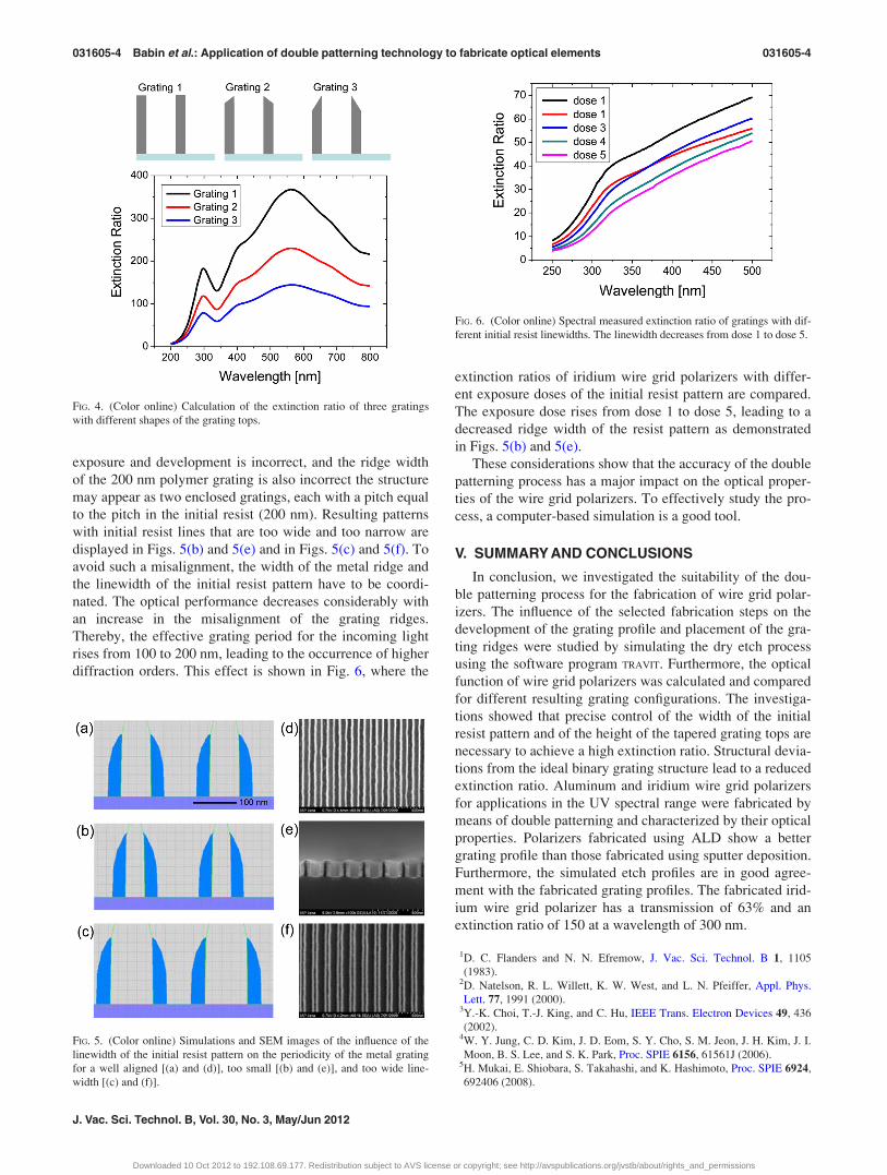
lated for an iridium wire grid polarizer, as shown in Fig. 4.
Grating 1 has a period of 100 nm, a height of 150 nm, and a
binary profile, while gratings 2 and 3 have tapered tops with
heights of 20 and 40 nm, respectively. It can be seen that the
extinction ratio decreases with the increasing height of the
tapered top. One reason is that the amount of grating mate-
rial is decreasing, leading to a higher transmission of TE-
polarized light, resulting in a reduction of the extinction ra-
tio. Another reason is that the nonhomogeneous grating
ridges are periodic with a period of 200 nm, leading to the
appearance of higher diffraction orders. A wire grid polarizer
usually works as a zero order grating with only the zeroth
diffraction order occurring.22 Higher diffraction orders com-
promise the optical performance of the polarizer. Hence, the
fabrication process should be optimized so that a nearly per-
fect binary grating profile is produced. The profile is better
in the process shown in Fig. 1 than in Fig. 2.
Moreover, the linewidth of the initial resist pattern gener-
ated using EBL is an important factor for the optical per-
formance of the grating. The distance between the ridges of
the 100 nm period grating is supposed to be equal, as shown
in Figs. 5(a) and 5(d). If the initial resist linewidth after
FIG. 1. (Color online) Simulated profiles and SEM images of the double pat-
terning process for the fabrication of iridium wire grid polarizers using
ALD. The initial resist pattern (a) is coated by ALD with iridium [(b) and
(e)] and afterwards anisotropically etched [(c) and (f)]. The resulting grating
with 100 nm period is depicted in (d) and (g).
FIG. 2. (Color online) Simulation and SEM images of the fabrication of alu-
minum wire grid polarizers using sputter deposition after the removal of the
tempered resist [(a) and (c)] and further ion beam etching [(b) and (d)].
FIG. 3. Spectral measured transmission and extinction ratio of the fabricated
iridium wire grid polarizer.
031605-3 Babin et al.: Application of double patterning technology to fabricate optical elements 031605-3
JVST B - Microelectronics and Nanometer Structures
Downloaded 10 Oct 2012 to 192.108.69.177. Redistribution subject to AVS license or copyright; see http://avspublications.org/jvstb/about/rights_and_permissions
exposure and development is incorrect, and the ridge width
of the 200 nm polymer grating is also incorrect the structure
may appear as two enclosed gratings, each with a pitch equal
to the pitch in the initial resist (200 nm). Resulting patterns
with initial resist lines that are too wide and too narrow are
displayed in Figs. 5(b) and 5(e) and in Figs. 5(c) and 5(f). To
avoid such a misalignment, the width of the metal ridge and
the linewidth of the initial resist pattern have to be coordi-
nated. The optical performance decreases considerably with
an increase in the misalignment of the grating ridges.
Thereby, the effective grating period for the incoming light
rises from 100 to 200 nm, leading to the occurrence of higher
diffraction orders. This effect is shown in Fig. 6, where the
extinction ratios of iridium wire grid polarizers with differ-
ent exposure doses of the initial resist pattern are compared.
The exposure dose rises from dose 1 to dose 5, leading to a
decreased ridge width of the resist pattern as demonstrated
in Figs. 5(b) and 5(e).
These considerations show that the accuracy of the double
patterning process has a major impact on the optical proper-
ties of the wire grid polarizers. To effectively study the pro-
cess, a computer-based simulation is a good tool.
V. SUMMARY AND CONCLUSIONS
In conclusion, we investigated the suitability of the dou-
ble patterning process for the fabrication of wire grid polar-
izers. The influence of the selected fabrication steps on the
development of the grating profile and placement of the gra-
ting ridges were studied by simulating the dry etch process
using the software program TRAVIT. Furthermore, the optical
function of wire grid polarizers was calculated and compared
for different resulting grating configurations. The investiga-
tions showed that precise control of the width of the initial
resist pattern and of the height of the tapered grating tops are
necessary to achieve a high extinction ratio. Structural devia-
tions from the ideal binary grating structure lead to a reduced
extinction ratio. Aluminum and iridium wire grid polarizers
for applications in the UV spectral range were fabricated by
means of double patterning and characterized by their optical
properties. Polarizers fabricated using ALD show a better
grating profile than those fabricated using sputter deposition.
Furthermore, the simulated etch profiles are in good agree-
ment with the fabricated grating profiles. The fabricated irid-
ium wire grid polarizer has a transmission of 63% and an
extinction ratio of 150 at a wavelength of 300 nm.
1D. C. Flanders and N. N. Efremow, J. Vac. Sci. Technol. B 1, 1105
(1983).2D. Natelson, R. L. Willett, K. W. West, and L. N. Pfeiffer, Appl. Phys.
Lett. 77, 1991 (2000).3Y.-K. Choi, T.-J. King, and C. Hu, IEEE Trans. Electron Devices 49, 436
(2002).4W. Y. Jung, C. D. Kim, J. D. Eom, S. Y. Cho, S. M. Jeon, J. H. Kim, J. I.
Moon, B. S. Lee, and S. K. Park, Proc. SPIE 6156, 61561J (2006).5H. Mukai, E. Shiobara, S. Takahashi, and K. Hashimoto, Proc. SPIE 6924,
692406 (2008).
FIG. 4. (Color online) Calculation of the extinction ratio of three gratings
with different shapes of the grating tops.
FIG. 5. (Color online) Simulations and SEM images of the influence of the
linewidth of the initial resist pattern on the periodicity of the metal grating
for a well aligned [(a) and (d)], too small [(b) and (e)], and too wide line-
width [(c) and (f)].
FIG. 6. (Color online) Spectral measured extinction ratio of gratings with dif-
ferent initial resist linewidths. The linewidth decreases from dose 1 to dose 5.
031605-4 Babin et al.: Application of double patterning technology to fabricate optical elements 031605-4
J. Vac. Sci. Technol. B, Vol. 30, No. 3, May/Jun 2012
Downloaded 10 Oct 2012 to 192.108.69.177. Redistribution subject to AVS license or copyright; see http://avspublications.org/jvstb/about/rights_and_permissions

6H. Dai, C. Bencher, Y. Chen, S. Sun, X. Xu, and C. Ngai, Proc. SPIE
7274, 72743G (2009).7M. Xu, H. P. Urbach, D. K. G. de Boer, and H. J. Cornelissen, Opt.
Express 13, 2303 (2005).8S. Babin and K. Bay, Proc. SPIE 7640, 764021 (2010).9Grating solver Development Co., http://www.gsolver.com.
10T. Weber, H.-J. Fuchs, H. Schmidt, E.-B. Kley, and A. Tunnermann, Proc.
SPIE 7205, 720504 (2009).11T. Weber, T. Kasebier, E.-B. Kley, and A. Tunnermann, Opt. Lett. 36, 445
(2011).12K. Kwon, S. Kang, S. Park, H. Sung, D. Kim, and J. Moon, J. Mater. Sci.
Lett. 18, 1197 (1999).13B. Wu and D. Chan, J. Microlith. Microfab. Microsyst. 2, 200 (2003).14L. Elmonser, A. Rhallabi, M. Gaillard, J. P. Landesman, A. Talneau,
F. Pommereau, and N. Bouadma, J. Vac. Sci. Technol. A 1, 126 (2007).
15E. Bogdanov, V. Kolobov, A. Kudryavtsev, and L. Tsendin, IEEE Confer-
ence on Plasma Science, Alberta, Canada, 2002, p. 2P12.16S. Babin, K. Bay, and S. Okulovsky, Proc. SPIE 6283, 62831R (2006).17E.-B. Kley, H. Schmidt, U. Zeitner, M. Banasch, and B. Schnabel,
“Enhanced E-beam pattern writing for nano-optics based on character pro-
jection,” Proc. SPIE 8352 (to be published).18T. Aaltonen, M. Ritala, V. Sammelselg, and M. Leskela, J. Electrochem.
Soc. 151, G489 (2004).19See website of Moxtek company, http://www.moxtek.com/optics/
broadband.html.20J. J. Wang, L. Chen, X. Liu, P. Sciortino, F. Liu, F. Walters, and X. Deng,
Appl. Phys. Lett. 89, 141105 (2006).21X. Liu et al., Nano Lett. 6, 2723 (2006).22T. Weber, T. Kasebier, A. Szeghalmi, M. Knez, E.-B. Kley, and A. Tun-
nermann, Nanoscale Res. Lett. 6, 558 (2011).
031605-5 Babin et al.: Application of double patterning technology to fabricate optical elements 031605-5
JVST B - Microelectronics and Nanometer Structures
Downloaded 10 Oct 2012 to 192.108.69.177. Redistribution subject to AVS license or copyright; see http://avspublications.org/jvstb/about/rights_and_permissions


![Overlay-Aware Detailed Routing for Self-Aligned Double Patterning … · 2021. 1. 31. · double patterning process is the better overlay control achieved by spacer protection [8]](https://img.pdfslide.us/doc/110x75/61110bd9b93f5b0fcd11cc4a/overlay-aware-detailed-routing-for-self-aligned-double-patterning-2021-1-31.jpg)