Embed Size (px)
Citation preview

Rev. 0.5 March 2012 Page 1 of 14 www.aosmd.com
AOZ1284EZBuck™ 4A Simple Buck Regulator
General Description
The AOZ1284 is a high voltage, high efficiency, simple to use, 4A buck regulator optimized for a variety of applications. The AOZ1284 works from a 3.0V to 36V input voltage range, and provides up to 4A of continuous output current. The output voltage is adjustable from 30V down to 0.8V.
The AOZ1284 integrates an N-channel high-side power MOSFET. The switching frequency can set from 200kHz to 2MHz with an external resistor. The soft-start time can be set with an external capacitor.
Features
3.0V to 36V operating input voltage range
50mΩ internal NMOS
Efficiency up to 95%
Adjustable soft-start
Output voltage adjustable from 0.8V to 30V
4A continuous output current
Adjustable switching frequency from 200kHz to 2MHz
Cycle-by-cycle current limit
Short-circuit protection
Over-voltage protection
Over-temperature protection
EPAD SO-8 package
Applications
Point of load DC/DC conversion
Set top boxes and cable modems
Automotive applications
DVD drives and HDDs
LCD Monitors & TVs
Telecom/Networking/Datacom equipment
Typical Application
Figure 1. 36V/4A Buck Regulator
Page 2 of 14 Rev. 0.5 March 2012 www.aosmd.com
AOZ1284
Ordering Information
Part Number Temperature Range Package Environmental
AOZ1284PI -40°C to +85°C EPAD SO-8 Green Product
AOZ1284PI-1
AOS Green Products use reduced levels of Halogens, and are also RoHS compliant.
Please visit www.aosmd.com/media/AOSGreenPolicy.pdf for additional information.
Pin Configuration
EPAD SO-8 (Top View)
Pin Description
Part Number Pin Name Pin Function
1 LX PWM Output Pin. Connect to inductor. 2 BST Bootstrap Voltage Pin. Driver supply for High Side NMOS. Connected to
100nF capacitor between BST and LX. 3 GND Ground Pin. 4 FSW Frequency Bias Pin. Connect to resistor to determine switching frequency. 5 COMP Compensation Pin. Connect to Resistor and Capacitor for system stability. 6 FB Feedback Pin. It is regulated to 0.8V. The FB pin is used to determine the
PWM output voltage via a resistor divider between the Output and Ground. 7 SS Soft Start Pin. 8 EN Enable Pin.
Exposed PAD VIN Supply Voltage Pin.
LX 1 EN8
BST 2 SS7
GND 3 FB6
FSW 4 COMP5
ExposedPAD
VIN
Page 3 of 14 Rev. 0.5 March 2012 www.aosmd.com
AOZ1284
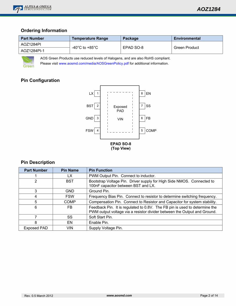
Functional Block
Absolute Maximum Ratings
Exceeding the Absolute Maximum Ratings may damage the device.
Parameter RatingSupply Voltage (VIN) 40VLX to GND -0.7V to VIN+0.3VEN, SS, FB and COMP to GND -0.3V to +6VBST to GND -0.3V to VLX+6VJunction Temperature (TJ) +150°CStorage Temperature (TS) -65°C to +150°CESD Rating HB Model(1) 2kV
Note:
1. Devices are inherently ESD sensitive, handling precautions are required. Human body model rating: 1.5kΩ in series with 100pF.
Recommended Operating Ratings
This device is not guaranteed to operate beyond the Recommended Operating Ratings.
Parameter RatingSupply Voltage (VIN) 3.0V to 36VOutput Voltage (VOUT) 0.8V to VIN*0.85VAmbient Temperature (TA) -40°C to +85°CPackage Thermal Resistance EPAD SO-8 (JA) 50°C/W

AOZ1284
Page 4 of 14 Rev. 0.5 March 2012 www.aosmd.com
Electrical Characteristics
TA = 25°C, VIN = 12V, VEN = 3V, VOUT = 3.3V, unless otherwise specified. Specifications in BOLD indicate a temperature range of -40 °C to +85 °C.
Symbol Parameter Conditions Min. Typ. Max Units VIN Supply Voltage 3 36 V
VUVLO Input Under-Voltage Lockout Threshold
VIN rising VIN falling
2.3
2.9 V
IIN Supply Current (Quiescent) IOUT = 0, VFB = 1V, VEN >1.2V
1 1.5 mA
IOFF Shutdown Supply Current VEN = 0V 10 µA
VFB Feedback Voltage TA=25oC 788 800 812 mV
VFB_LOAD Load Regulation 0.4A < Load < 3.6A 0.5 %
VFB_LINE Line Regulation Io=2A 0.03 %/V
IFB Feedback Voltage Input Current VFB = 800mV 0.5 1 µA
Enable
VEN_OFF
VEN_ON
EN Input Threshold Off threshold
On threshold
1.2
0.4 V
VEN_HYS EN Input Hysteresis 200 mV
Current Limit
Peak Current Limit
1284 5 6 A
1284-1 5.5 6.5
Soft Start (SS)
ISS Soft Start Source Current 2 2.5 3 µA
Modulator
fO Frequency RF = 270kΩ RF = 46.6kΩ
160 0.8
200 1
240 1.2
kHz MHz
DMAX Maximum Duty Cycle fO = 1MHz 87 %
TON_MIN Minimum On Time 150 ns
GVEA Error Amplifier Voltage Gain 500 V/V
GEA Error Amplifier Transconductance 170 µA/V
GCS Current Sense Circuit Transconductance,
4.5 A/V
Power Stage Output
ILEAKAGE NMOS Leakage VEN=0V, VLX=0V 10 µA
RDSON1 NMOS On- Resistance 50 70 mΩ
Thermal Protection
TSD Thermal Shutdown Threshold 145 °C
TSD_HYS Thermal Shutdown Hysteresis 45 °C
Page 5 of 14 Rev. 0.5 March 2012 www.aosmd.com
AOZ1284
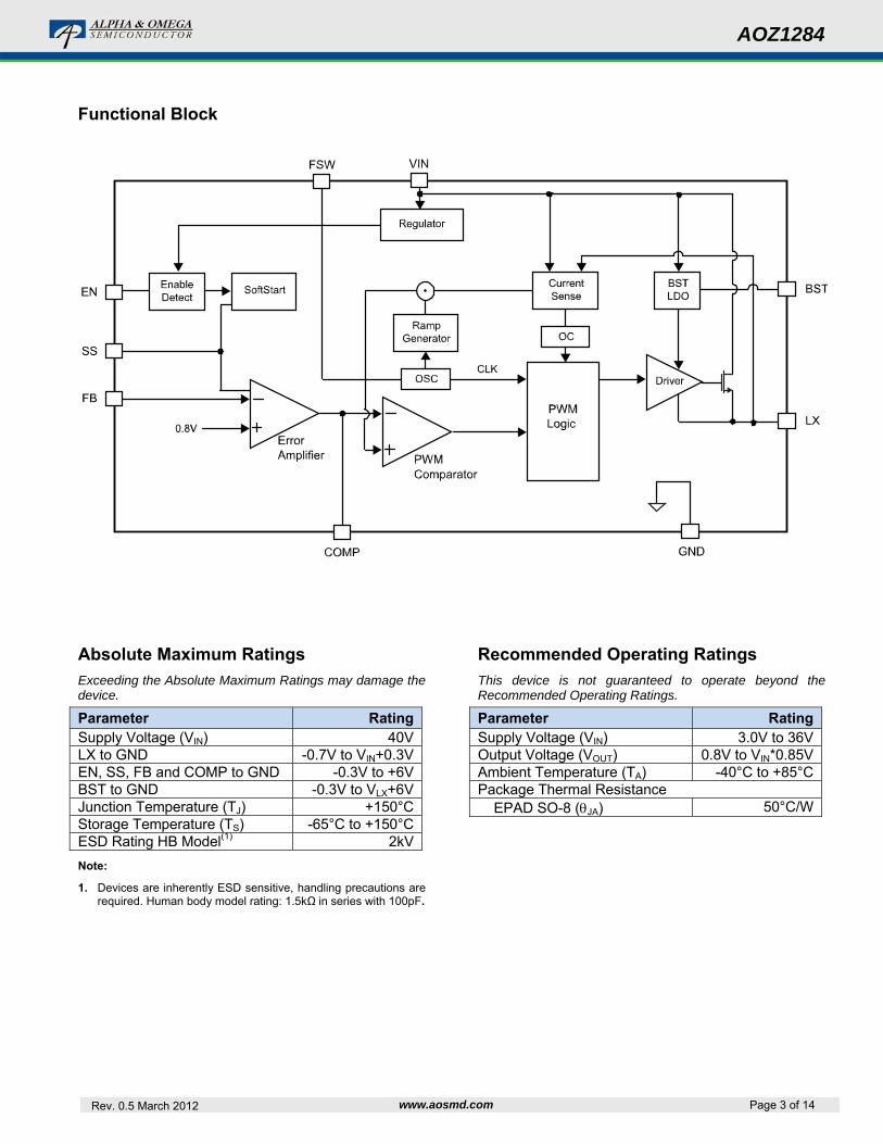
Typical Performance Characteristics
TA = 25°C, VIN = 24V, VEN = 5V, VOUT = 5V, unless otherwise specified.

Page 6 of 14 Rev. 0.5 March 2012 www.aosmd.com
AOZ1284
Efficiency Curves

Page 7 of 14 Rev. 0.5 March 2012 www.aosmd.com
AOZ1284
Detailed Description
The AOZ1284 is a current-mode step down regulator with integrated high side NMOS switch. It operates from a 3V to 36V input voltage range and supplies up to 4A of load current. Features include enable control, Power-On Reset, input under voltage lockout, external soft-start and thermal shut down.
The AOZ1284 is available in EPAD SO-8 package.
Enable and Soft Start
The AOZ1284 has external soft start feature to limit in-rush current and ensure the output voltage ramps up smoothly to regulation voltage. A soft start process begins when the input voltage rises to 3V and voltage on EN pin is HIGH. In soft start process, a 2.5µA internal current source charges the external capacitor at SS. As the SS capacitor is charged, the voltage at SS rises. The SS voltage clamps the reference voltage of the error amplifier, therefore output voltage rising time follows the SS pin voltage. With the slow ramping up output voltage, the inrush current can be prevented. Minimum external soft-start capacitor 850pF is required, and the corresponding soft-start time is about 200µs.
The EN pin of the AOZ1284 is active high. Connect the EN pin to a voltage between 1.2V to 5V if enable function is not used. Pull it to ground will disable the AOZ1284. Do not leave it open. The voltage on EN pin must be above 1.2V to enable the AOZ1284. When voltage on EN pin falls below 0.4V, the AOZ1284 is disabled. If an application circuit requires the AOZ1284 to be disabled, an open drain or open collector circuit should be used to interface to EN pin.
Steady-State Operation
Under steady-state conditions, the converter operates in fixed frequency and Continuous-Conduction Mode (CCM).
The AOZ1284 integrates an internal N-MOSFET as the high-side switch. Inductor current is sensed by amplifying the voltage drop across the drain to source of the high side power MOSFET. Since the N-MOSFET requires a gate voltage higher than the input voltage, a boost capacitor connected between LX pin and BST pin drives the gate. The boost capacitor is charged while LX is low. An internal 10Ω switch from LX to GND is used to insure that LX is pulled to GND even in the light load. Output voltage is divided down by the external voltage divider at the FB pin. The difference of the FB pin voltage and reference is amplified by the internal transconductance error amplifier. The error voltage, which shows on the
COMP pin, is compared against the current signal, which is sum of inductor current signal and ramp compensation signal, at PWM comparator input. If the current signal is less than the error voltage, the internal high-side switch is on. The inductor current flows from the input through the inductor to the output. When the current signal exceeds the error voltage, the high-side switch is off. The inductor current is freewheeling through the Schottky diode to output.
Switching Frequency
The AOZ1284 switching frequency can be programmed by external resistor. External resistor value can be calculated by following formula.
kkHzf
kRFO
5)(
50000)(
Some standard values of RF for most commonly used switching frequency are listed in Table 1.
fO(Hz) RF (kΩ) 200k 270 500k 100 1M 46.6
Table 1
Output Voltage Programming
Output voltage can be set by feeding back the output to the FB pin with a resistor divider network. In the application circuit shown in Figure 1 (Typical Application). The resistor divider network includes R2 and R3. Usually, a design is started by picking a fixed R3 value and calculating the required R2 with equation below.
2
118.0R
RVO
Some standard value of R1, R2 for most commonly used output voltage values are listed below in Table 2.
VO (V) R1 (kΩ) R2 (kΩ) 0.8 1.0 Open 1.2 4.99 10 1.5 10 11.5 1.8 12.7 10.2 2.5 21.5 10 3.3 31.6 10 5.0 52.3 10
Table 2
Page 8 of 14 Rev. 0.5 March 2012 www.aosmd.com
AOZ1284
Combination of R1 and R2 should be large enough to avoid drawing excessive current from the output, which will cause power loss.
Protection Features
The AOZ1284 has multiple protection features to prevent system circuit damage under abnormal conditions.
Over Current Protection (OCP)
The sensed inductor current signal is also used for over current protection. Since the AOZ1284 employs peak current mode control, the COMP pin voltage is proportional to the peak inductor current. The COMP pin voltage is limited to be between 0.4V and 2.5V internally. The peak inductor current is automatically limited cycle by cycle.
The cycle by cycle current limit threshold is internally set. When the load current reaches the current limit threshold, the cycle by cycle current limit circuit turns off the high side switch immediately to terminate the current duty cycle. The inductor current stop rising. The cycle by cycle current limit protection directly limits inductor peak current. The average inductor current is also limited due to the limitation on peak inductor current. When cycle by cycle current limit circuit is triggered, the output voltage drops as the duty cycle decreasing.
The AOZ1284 has internal short circuit protection to protect itself from catastrophic failure under output short circuit conditions. The FB pin voltage is proportional to the output voltage. Whenever FB pin voltage is below 0.2V, the short circuit protection circuit is triggered.
Power-On Reset (POR)
A power-on reset circuit monitors the input voltage. When the input voltage exceeds 2.9V, the converter starts operation. When input voltage falls below 2.3V, the converter will stop switching.
Thermal Protection
An internal temperature sensor monitors the junction temperature. It shuts down the internal control circuit and high side NMOS if the junction temperature exceeds 145ºC. The regulator will restart automatically under the control of soft-start circuit when the junction temperature decreases to 100ºC.
Application Information
The basic AOZ1284 application circuit is shown in Figure 1. Component selection is explained below.
Input capacitor
The input capacitor (C1 in Figure 1) must be connected to the VIN pin and GND pin of the AOZ1284 to maintain steady input voltage and filter out the pulsing input current. The voltage rating of input capacitor must be greater than maximum input voltage plus ripple voltage.
The input ripple voltage can be approximated by equation below:
NI
O
NI
O
NI
ONI V
V
V
V
Cf
IV
1
Since the input current is discontinuous in a buck converter, the current stress on the input capacitor is another concern when selecting the capacitor. For a buck circuit, the RMS value of input capacitor current can be calculated by:
IN
O
IN
OORMSCIN V
V
V
VII 1_
if let m equal the conversion ratio:
mV
V
IN
O
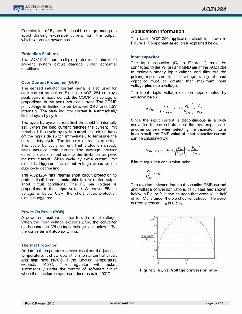
The relation between the input capacitor RMS current and voltage conversion ratio is calculated and shown below in Figure 2. It can be seen that when VO is half of VIN, CIN is under the worst current stress. The worst current stress on CIN is 0.5·IO.
Figure 2. ICIN vs. Voltage conversion ratio
0 0.5 10
0.1
0.2
0.3
0.4
0.50.5
0
I CIN_RMS m( )
I O
10 m
Page 9 of 14 Rev. 0.5 March 2012 www.aosmd.com
AOZ1284
For reliable operation and best performance, the input capacitors must have current rating higher than ICIN-
RMS at worst operating conditions. Ceramic capacitors are preferred for input capacitors because of their low ESR and high ripple current rating. Depending on the application circuits, other low ESR tantalum capacitor or aluminum electrolytic capacitor may also be used. When selecting ceramic capacitors, X5R or X7R type dielectric ceramic capacitors are preferred for their better temperature and voltage characteristics. Note that the ripple current rating from capacitor manufactures is based on certain amount of life time. Further de-rating may be necessary for practical design requirement.
Inductor
The inductor is used to supply constant current to output when it is driven by a switching voltage. For given input and output voltage, inductance and switching frequency together decide the inductor ripple current, which is:
IN
OOL V
V
Lf
VI 1
The peak inductor current is:
2L
OLPEAKI
II
High inductance gives low inductor ripple current but requires larger size inductor to avoid saturation. Low ripple current reduces inductor core losses. It also reduces RMS current through inductor and switches, which results in less conduction loss.
When selecting the inductor, make sure it is able to handle the peak current without saturation even at the highest operating temperature.
The inductor takes the highest current in a buck circuit. The conduction loss on inductor needs to be checked for thermal and efficiency requirements.
Surface mount inductors in different shape and styles are available from Wurth, Sumida, Coilcraft, and Murata. Shielded inductors are small and radiate less EMI noise. But they cost more than unshielded inductors. The choice depends on EMI requirement, price and size.
Output Capacitor
The output capacitor is selected based on the DC output voltage rating, output ripple voltage specification and ripple current rating.
The selected output capacitor must have a higher rated voltage specification than the maximum desired output voltage including ripple. De-rating needs to be considered for long term reliability.
Output ripple voltage specification is another important factor for selecting the output capacitor. In a buck converter circuit, output ripple voltage is determined by inductor value, switching frequency, output capacitor value and ESR. It can be calculated by the equation below:
O
COLO CfESRIV
8
1
where;
CO is output capacitor value and
ESRCO is the Equivalent Series Resistor of output capacitor.
When low ESR ceramic capacitor is used as output capacitor, the impedance of the capacitor at the switching frequency dominates. Output ripple is mainly caused by capacitor value and inductor ripple current. The output ripple voltage calculation can be simplified to:
OLO Cf
IV
8
1
If the impedance of ESR at switching frequency dominates, the output ripple voltage is mainly decided by capacitor ESR and inductor ripple current. The output ripple voltage calculation can be further simplified to:
COLO ESRIV
For lower output ripple voltage across the entire operating temperature range, X5R or X7R dielectric type of ceramic, or other low ESR tantalum capacitor or aluminum electrolytic capacitor may also be used as output capacitors.
In a buck converter, output capacitor current is continuous. The RMS current of output capacitor is decided by the peak to peak inductor ripple current. It can be calculated by:
12_
LRMSCO
II
Usually, the ripple current rating of the output capacitor is a smaller issue because of the low current stress. When the buck inductor is selected to be very small and inductor ripple current is high, output capacitor could be overstressed.
Page 10 of 14 Rev. 0.5 March 2012 www.aosmd.com
AOZ1284
Schottky Diode Selection
The external freewheeling diode supplies the current to the inductor when the high side NMOS switch is off. To reduce the losses due to the forward voltage drop and recovery of diode, Schottky diode is recommended to use. The maximum reverse voltage rating of the chosen Schottky diode should be greater than the maximum input voltage, and the current rating should be greater than the maximum load current.
Low Input operation
When VIN is lower than 4.5V, such as 3.0V, an external 5V is required to add into the BST pin for proper operation.
Loop Compensation
The AOZ1284 employs peak current mode control for easy use and fast transient response. Peak current mode control eliminates the double pole effect of the output L&C filter. It greatly simplifies the compensation loop design.
With peak current mode control, the buck power stage can be simplified to be a one-pole and one-zero system in frequency domain. The pole is dominant pole and can be calculated by:
LOP RC
f
2
11
The zero is a ESR zero due to output capacitor and its ESR. It is can be calculated by:
COOZ ESRC
f
2
11
where;
CO is the output filter capacitor;
RL is load resistor value and
ESRCO is the equivalent series resistance of output capacitor.
The compensation design is actually to shape the converter close loop transfer function to get desired gain and phase. Several different types of compensation network can be used for AOZ1284. For most cases, a series capacitor and resistor network connected to the COMP pin sets the pole-zero and is adequate for a stable high-bandwidth control loop.
In the AOZ1284, FB pin and COMP pin are the inverting input and the output of internal transconductance error amplifier. A series R and C compensation network connected to COMP provides one pole and one zero. The pole is:
VEAC
EAP GC
Gf
22
where;
GEA is the error amplifier transconductance, which is 200·10-6 A/V;
GVEA is the error amplifier voltage gain, which is 500 V/V and
CC is compensation capacitor.
The zero given by the external compensation network, capacitor CC (C5 in Figure 1) and resistor RC (R1 in Figure 1), is located at:
CCZ RC
f
2
12
To design the compensation circuit, a target crossover frequency fC for close loop must be selected. The system crossover frequency is where control loop has unity gain. The crossover frequency is also called the converter bandwidth. Generally a higher bandwidth means faster response to load transient. However, the bandwidth should not be too high due to system stability concern. When designing the compensation loop, converter stability under all line and load condition must be considered.
Usually, it is recommended to set the bandwidth to be less than 1/10 of switching frequency.
The strategy for choosing RC and CC is to set the cross over frequency with RC and set the compensator zero with CC. Using selected crossover frequency, fC, to calculate RC:
CSEA
O
FB
OCC GG
C
V
VfR
2
where;
fC is desired crossover frequency;
VFB is 0.8V;
GEA is the error amplifier transconductance, which is 200·10-6 A/V and
GCS is the current sense circuit transconductance, which is 4.5 A/V.
The compensation capacitor CC and resistor RC together make a zero. This zero is put somewhere close to the dominate pole fp1 but lower than 1/5 of selected crossover frequency. CC can is selected by:
12
5.1
PCC fR
C

Page 11 of 14 Rev. 0.5 March 2012 www.aosmd.com
AOZ1284
Equation above can also be simplified to:
C
LOC R
RCC
Easy to use application software which helps to design and simulate the compensation loop can be found at www.aosmd.com.
Thermal management and layout consideration
In the AOZ1284 buck regulator circuit, high pulsing current flows through two circuit loops. The first loop starts from the input capacitors, to the VIN pin, to the LX pins, to the filter inductor, to the output capacitor and load, and then return to the input capacitor through ground. Current flows in the first loop when the high side switch is on. The second loop starts from inductor, to the output capacitors and load, to the GND pin of the AOZ1284, to the LX pins of the AOZ1284. Current flows in the second loop when the low side diode is on.
In PCB layout, minimizing the two loops area reduces the noise of this circuit and improves efficiency. A ground plane is recommended to connect input capacitor, output capacitor, and GND pin of the AOZ1284.
In the AOZ1284 buck regulator circuit, the three major power dissipating components are the AOZ1284, external diode and output inductor. The total power dissipation of converter circuit can be measured by input power minus output power.
OOININlosstotal IVIVP _
The power dissipation of inductor can be approximately calculated by output current and DCR of inductor.
1.12_ inductorOlossinductor RIP
The power dissipation of diode is
IN
OFOlossdiode V
VVIP 1_
The actual AOZ1284 junction temperature can be calculated with power dissipation in the AOZ1284 and thermal impedance from junction to ambient.
ambientJA
lossdiodelossinductorlosstotaljunction T
PPPT
___
The maximum junction temperature of AOZ1284 is 145ºC, which limits the maximum load current capability.
The thermal performance of the AOZ1284 is strongly affected by the PCB layout. Extra care should be taken by users during design process to ensure that the IC will operate under the recommended environmental conditions.
Several layout tips are listed below for the best electric and thermal performance. The Figure 3 (a) and (b) give the example of layout for AOZ1284A and AOZ1284D respectively.
1. Do not use thermal relief connection to the VIN and the GND pin. Pour a maximized copper area to the GND pin and the VIN pin to help thermal dissipation.
2. Input capacitor should be connected to the VIN pin and the GND pin as close as possible.
3. Make the current trace from LX pins to L to Co to the GND as short as possible.
4. Pour copper plane on all unused board area and connect it to stable DC nodes, like VIN, GND or VOUT.
5. Keep sensitive signal trace such as trace connected with FB pin and COMP pin far away from the LX pins.

AOZ1284
Page 12 of 14 Rev. 0.5 March 2012 www.aosmd.com
Package Dimensions, SO-8 EP1
Notes:1. Package body sizes exclude mold flash and gate burrs.2. Dimension L is measured in gauge plane.3. Tolerance 0.10mm unless otherwise specified.4. Controlling dimension is millimeter, converted inch dimensions are not necessarily exact.5. Die pad exposure size is according to lead frame design.6. Followed from JEDEC MS-012
Symbols
A
A1
A2
B
C
D
D0
D1
E
e
E1
E2
E3
L
y
| L1–L1' |
L1
Dimensions in millimeters
RECOMMENDED LAND PATTERN
Min.
1.40
0.00
1.40
0.31
0.17
4.80
3.20
3.10
5.80
—
3.80
2.21
0.40
—
0°
—
D0
UNIT: mm
Nom.
1.55
0.05
1.50
0.406
—
4.96
3.40
3.30
6.00
1.27
3.90
2.41
0.40 REF
0.95
—
3°
0.04
1.04 REF
Max.
1.70
0.10
1.60
0.51
0.25
5.00
3.60
3.50
6.20
—
4.00
2.61
1.27
0.10
8°
0.12
Dimensions in inches
D1
E1 EE3E2
Note 5
L1'
L1
L
Gauge plane0.2500
C
D
7 (4x)
B
3.70
2.20
2.87
2.71
5.74
1.270.80
0.635
eA1
A2 A
Symbols
A
A1
A2
B
C
D
D0
D1
E
e
E1
E2
E3
L
y
| L1–L1' |
L1
Min.
0.055
0.000
0.055
0.012
0.007
0.189
0.126
0.122
0.228
—
0.150
0.087
0.016
—
0°
—
Nom.
0.061
0.002
0.059
0.016
—
0.195
0.134
0.130
0.236
0.050
0.153
0.095
0.016 REF
0.037
—
3°
0.002
0.041 REF
Max.
0.067
0.004
0.063
0.020
0.010
0.197
0.142
0.138
0.244
—
0.157
0.103
0.050
0.004
8°
0.005
Page 13 of 14 Rev. 0.5 March 2012 www.aosmd.com
AOZ1284
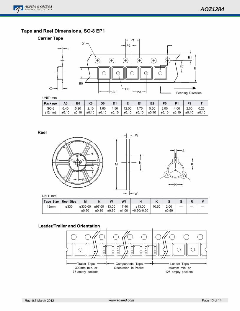
Tape and Reel Dimensions, SO-8 EP1
Carrier Tape
Reel
Tape Size
12mm
Reel Size
ø330
M
ø330.00±0.50
Package
SO-8(12mm)
A0
6.40±0.10
B0
5.20±0.10
K0
2.10±0.10
D0
1.60±0.10
D1
1.50±0.10
E
12.00±0.10
E1
1.75±0.10
E2
5.50±0.10
P0
8.00±0.10
P1
4.00±0.10
P2
2.00±0.10
T
0.25±0.10
N
ø97.00±0.10
K0
UNIT: mm
B0
G
M
W1
S
K
H
N
W
V
R
Trailer Tape300mm min. or
75 empty pockets
Components TapeOrientation in Pocket
Leader Tape500mm min. or
125 empty pockets
A0
P1
P2
Feeding DirectionP0
E2
E1
E
D0
T
D1
W
13.00±0.30
W1
17.40±1.00
H
ø13.00+0.50/-0.20
K
10.60
S
2.00±0.50
G
—
R
—
V
—
Leader/Trailer and Orientation
UNIT: mm
Page 14 of 14 Rev. 0.5 March 2012 www.aosmd.com
AOZ1284
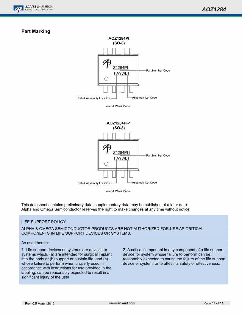
Part Marking
This datasheet contains preliminary data; supplementary data may be published at a later date. Alpha and Omega Semiconductor reserves the right to make changes at any time without notice.
LIFE SUPPORT POLICY
ALPHA & OMEGA SEMICONDUCTOR PRODUCTS ARE NOT AUTHORIZED FOR USE AS CRITICAL COMPONENTS IN LIFE SUPPORT DEVICES OR SYSTEMS.
As used herein:
1. Life support devices or systems are devices or systems which, (a) are intended for surgical implant into the body or (b) support or sustain life, and (c) whose failure to perform when properly used in accordance with instructions for use provided in the labeling, can be reasonably expected to result in a significant injury of the user.
2. A critical component in any component of a life support, device, or system whose failure to perform can be reasonably expected to cause the failure of the life support device or system, or to affect its safety or effectiveness.
Z1284PI
FAYPart Number Code
Assembly Lot Code
Year & Week Code
WLT
Fab & Assembly Location
Z1284PI1
FAYPart Number Code
Assembly Lot Code
Year & Week Code
WLT
Fab & Assembly Location
AOZ1284PI(SO-8)
AOZ1284PI-1(SO-8)