Embed Size (px)
Citation preview

„This material is posted here with permission of the IEEE. Such permission of the IEEE does not in any way imply IEEE endorsement of any of ETH Zürich’s products or services. Internal or personal use of this material is permitted. However, permission to reprint/republish this material for advertising or promo-tional purposes or for creating new collective works for resale or redistribution must be obtained from the IEEE by writing to [email protected]. By choosing to view this document you agree to all provisions of the copyright laws protecting it.”
An Optimized 5 kW, 147 W/in3 Telecom Phase-Shift DC-DC Converter with Magnetically Integrated Current Doubler
U. Badstuebner, J. Biela, B. Faessler, D. Hoesli and J.W. Kolar
Power Electronic Systems Laboratory, ETH Zurich ETH-Zentrum, ETL H12, Physikstrasse 3
CH-8092 Zurich, Switzerland Email: [email protected]

An Optimized 5 kW, 147 W/in3 Telecom Phase-ShiftDC-DC Converter with Magnetically Integrated Current Doubler
U. Badstuebner, J. Biela, B. Faessler, D. Hoesli and J.W. KolarPower Electronic Systems Laboratory, ETH Zurich
ETH-Zentrum, ETL H12, Physikstrasse 3CH-8092 Zurich, Switzerland
Email: [email protected]
Abstract- In the last decade there has been a tremendous growthin the number of data centers due to the increasing demand forinternet services. At the same time, the cost for energy and materialshave increased because of reducing resources and increased demand.That has caused a change in the driving forces for new powersupply development, with more consideration on power density andefficiency.
The commonly used DC-DC converter in the power supply unit(PSU) for data centers and telecom applications are full bridge phase-shift converters since they meet the demands of high power levelsand concurrently efficient power conversion as well as a compactdesign. The constant operating frequency allows a simple controland EMI design.
To develop a new converter with higher power density and/orhigh efficiency the designer has a lot of degrees of freedom. Anoptimization procedure, based on comprehensive analytical models,has been developed and leads to the optimal parameters (e.g.switching frequency or transformer design) to achieve the mostcompact and/or efficient design.
In this paper an volume optimized 400 V/48 V phase-shift DC-DCconverter with current doubler rectifier based on analytical modelsis constructed. The power density of the converter is increasedby integrating the output inductors in the transformers core. Theintrinsic voltage ringing of the rectifier diodes is damped by a losslessmagnetic snubber, which feeds ringing energy to the output.
Experimental results prove the theoretical analytical models andthe design procedure. The 5kW DC-DC converter prototype had apower density of 9kW/liter (147W/in3) and a maximum efficiency of94.75 %.
I. INTRODUCTION
In the area of power electronic converter systems there is ageneral trend to higher power densities that is driven by costreduction, increased functionality and in some applications by thelimited weight/space (e.g. automotive, aircraft) [1]. Moreover,when used in the continuously growing data centers, these con-verter focus more on high efficiencies in order to decrease thecooling effort and save energy.
In power supply units (PSU) for telecommunication facilitiesor data centers, DC-DC converters are utilized for converting therectified mains voltage to intermediate voltage levels for powerdistribution. In the literature many different topologies havebeen proposed for this application but for high power conversionusually full bridge topologies operating with soft switching, likea series-parallel resonant converter or phase shift converter withcurrent doubler are applied, since these are relatively simple,robust and meet the demands of high power density and efficiency.
TABLE I: Specifications for the proposed IT DC-DC converter.
Input voltageOutput voltageOutput powerOutput ripple voltageMax. ambient temperatureMax. height
VINVOaTPOaTVP ph
h
400 V48... .54V5kW
300 mVp p45 °C
1 U (; 44 mm)
a) 5kW prototype of the proposed 400 V/48..54V DC-DC converter:Height: 1 U, volume: 0.56 liter, power density: 147 W/in3 (9 kW/liter)
+O
vl7V
b) Schematic of the phase-shift full bridge converter with currentdoubler rectifier
Fig. 1: Phase-shift DC-DC converter with current doubler output
The design of the DC-DC converter has many degrees offreedom which complicates the selection of the best topologyand the determination of the component values, which result inthe best solution. In order to enable a direct design process forthe solution with the highest power density/efficiency an opti-mization procedure, based on comprehensive analytical modelsand equations considering the losses in the semiconductors, inthe magnetic devices and the other passive components, has beendeveloped [2]. With this procedure the optimal design parametersin respect to power density and/or efficiency, such as switchingfrequency, component values for the capacitors and inductors,magnetic devices geometry or total heat sink volume, respectively,could determined.
In [2], this procedure has been utilized for optimizing andcomparing a series-parallel resonant converter and phase-shiftconverters with capacitive and current doubler output with respectto power density and efficiency. A theoretical power densityof lOkW/liter and of 8.6kW/liter have been achieved for theresonant converter and/or the phase-shift converter with currentdoubler. However, for the sake of brevity the design equationsonly could be shortly summarized. Therefore, the derivation of the
978-1-422-2812-0/09/$25.00 02009 IEEE
CINV
21
analytical models for the currents/voltages as well as for designingthe magnetic components are presented in Section II of thispaper. There, the design of the transformer with integrated outputinductors and its integrated thermal management is also discussed.Furthermore, a new lossless snubber circuit for the rectifier diodes,which could experience high overvoltages in current doublercircuits in principle, is presented. The optimization procedureis discussed in Section III. The snubber circuit, the analyticalmodels applied in the optimization procedure as well as the powerdensity prediction are validated with measurement results on a5 kW prototype with a power density of 9 kW/liter in Section IV.
II. PHASE-SHIFT DC-DC CONVERTER WITH CURRENTDOUBLER RECTIFIER
The full bridge phase-shift DC-DC converter with currentdoubler rectifier in Fig. 1 fulfills the demands on a robust andsimple design with a high power density and high efficiency.As shown in Fig. lb), the converter consists of 4 switches aspart of the full bridge, a transformer which provides galvanicisolation and transforms the voltage (400V to 48..54 V), and therectifier with the two output inductors and diodes. As shownlater in this section, the two output inductors can be integratedin the transformer, in order to reduce the volume of the magneticcomponents and save the space required for interconnections andmounting. In order to derive the analytical models in subsectionII-A, the relative simple control scheme and basic functionalitiesof the phase-shift converters are shortly explained in the following.Due to parasitic elements, overvoltages occur across the rectifierdiodes, so that a snubber circuit is required. Therefore, threelossless snubber circuits are presented and compared on the basisof measurement results in subsection 11-B.
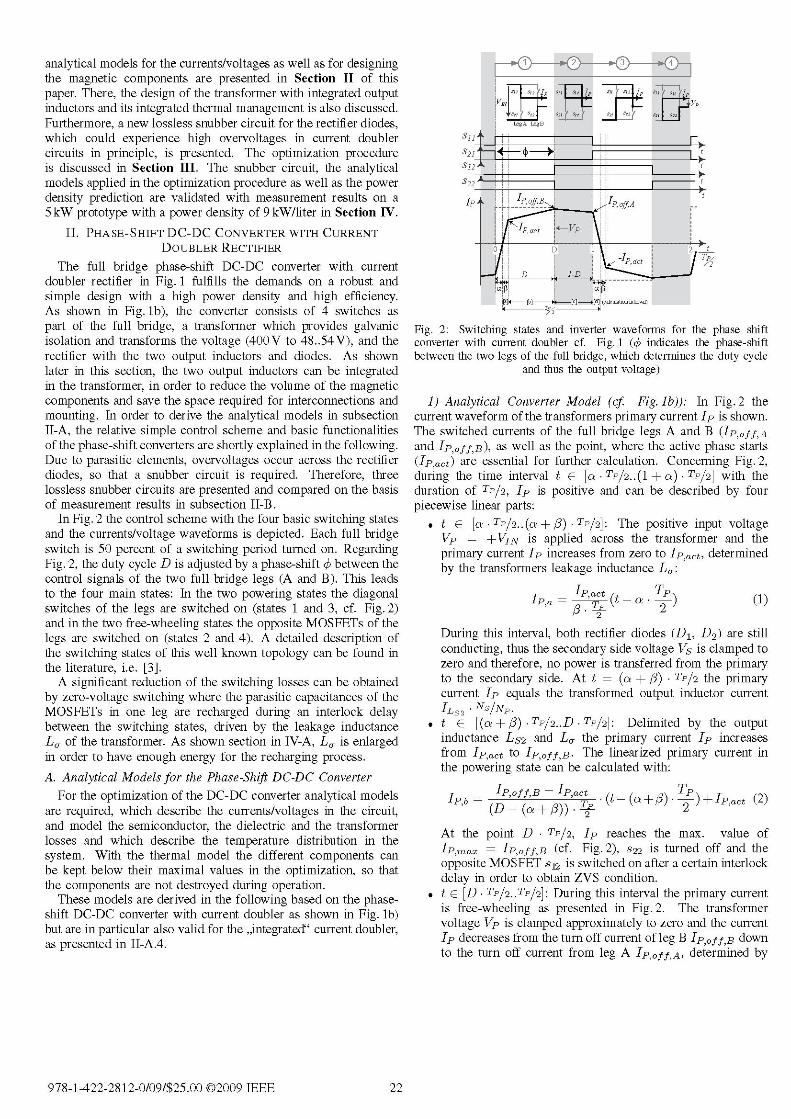
In Fig. 2 the control scheme with the four basic switching statesand the currents/voltage waveforms is depicted. Each full bridgeswitch is 50 percent of a switching period turned on. RegardingFig. 2, the duty cycle D is adjusted by a phase-shift e between thecontrol signals of the two full bridge legs (A and B). This leadsto the four main states: In the two powering states the diagonalswitches of the legs are switched on (states 1 and 3, cf. Fig. 2)and in the two free-wheeling states the opposite MOSFETs of thelegs are switched on (states 2 and 4). A detailed description ofthe switching states of this well known topology can be found inthe literature, i.e. [3].A significant reduction of the switching losses can be obtained
by zero-voltage switching where the parasitic capacitances of theMOSFETs in one leg are recharged during an interlock delaybetween the switching states, driven by the leakage inductanceL, of the transformer. As shown section in IV-A, L, is enlargedin order to have enough energy for the recharging process.A. Analytical Models for the Phase-Shift DC-DC Converter
For the optimization of the DC-DC converter analytical modelsare required, which describe the currents/voltages in the circuit,and model the semiconductor, the dielectric and the transformerlosses and which describe the temperature distribution in thesystem. With the thermal model the different components canbe kept below their maximal values in the optimization, so thatthe components are not destroyed during operation.
These models are derived in the following based on the phase-shift DC-DC converter with current doubler as shown in Fig. lb)but are in particular also valid for the ,,integrated" current doubler,as presented in II-A.4.
S2J
S2/
IP
i,
:!I,off,Act
I Tp2
Fig. 2: Switching states and inverter waveforms for the phase shiftconverter with current doubler cf. Fig. 1 (b indicates the phase-shiftbetween the two legs of the full bridge, which determines the duty cycle
and thus the output voltage)
1) Analytical Converter Model (cf. Fig. lb)): In Fig. 2 thecurrent waveform of the transformers primary current Ip is shown.The switched currents of the full bridge legs A and B (Ip,off,Aand IP,off,B), as well as the point, where the active phase starts('p,act) are essential for further calculation. Concerning Fig.2,during the time interval t e [a. TP/2.. (1 + a) TP/2] with theduration of TP/2, Ip is positive and can be described by fourpiecewise linear parts:
t C [a TP/2.. (a + 73) TP/2]: The positive input voltageVP = +VIN is applied across the transformer and theprimary current Ip increases from zero to 1Pact, determinedby the transformers leakage inductance L,:
l p,act Tp3P,a= T(t- 2)
2(1)
During this interval, both rectifier diodes (D1, D2) are stillconducting, thus the secondary side voltage Vs is clamped tozero and therefore, no power is transferred from the primaryto the secondary side. At t = (a + 73) TP/2 the primarycurrent Ip equals the transformed output inductor currentILS2 *NS/NP.t C [(aV + 73) TP/2..D TP/2]: Delimited by the outputinductance LS2 and L, the primary current Ip increasesfrom IP,act to IP,off,B. The linearized primary current inthe powering state can be calculated with:
b -IpoffB-IP,act . (t- ( + 3) P ) + 'p,act (2)(D-(-73) 2P 2
At the point D * TP/2, Ip reaches the max. value ofIP,max = IP,off,B (cf. Fig.2), s22 is turned off and theopposite MOSFET s12 is switched on after a certain interlockdelay in order to obtain ZVS condition.t C [D * TP/2..TP/2]: During this interval the primary currentis free-wheeling as presented in Fig. 2. The transformervoltage Vp is clamped approximately to zero and the currentIp decreases from the turn off current of leg B IP,off,B downto the turn off current from leg A IP,off,A, determined by
978-1-422-2812-0/09/$25.00 02009 IEEE 22
L, in series with LS1,2 (NP/Ns)2IP,off,A - IP,off,B TDTI =PXof) A-IP °ff(t ) + IpP,off,B (3)1P,c (1-D).T7j -D 2 3
At t =TP/2, the high side switch of leg A (s3j) is turned offand diagonal switch 821 is turned on.t C [TP/2.. (1 + C) TP/2]: While changing from the free-wheeling state to the active state, the negative input voltageVP =-VIN is applied to the transformer and Ip decreasesto OA determined by L,:
,d = ,Off,A (t- ) + IPoffAa -TP 22
where AIOUT is the peak-to-peak value of the ripple currentIC,, in the output capacitor. The DC component IOUT canbe simply calculated with the required output power POUT andthe output voltage VOUT:
(8)IOUT =POUTVOUTThe current ripple AIOUT is defined by the factor kl, a variableparameter for the optimization (k, C [0..0.2]), since the allowedcurrent ripple defines the volume of the inductors and outputcapacitance:
(4)
After that interval, the second half of the switching period startswith the first interval (a) again but with changed direction ofprimary current and voltage.
With the current waveform given in (1)-(4) the RMS value ofIp (important for the loss calculation) can be calculated:
1rm 2d ) 2 D TP
jP,rTns - 2 TPJjT P,a dt + J jPbbdt+T2 (1+ a) TTp+ 2JTyFd+ 2
22 'p,d dtl
The duty cycle D, which defines the converter output voltage,is divided into the effective duty cycle De (power transfer),determined by twice of the output voltage VOUT and secondaryside voltage VIN NP/Ns, and a duty cycle loss Di = (a + /3)(cf. Fig. 2) caused by the transformers leakage inductance L.
D =De + Di (5)2. VOUTD ~~+ (a +73) (6)VIN NP/Ns
The calculations presented so far, require the knowledge of aand 73. Furthermore, besides the calculation of the RMS-value inorder to calculated the conduction losses, the turn off currentsIP,off,A,B have to be calculated for the switching losses andfor solving the equations for a and /3,which is presented in thefollowing.
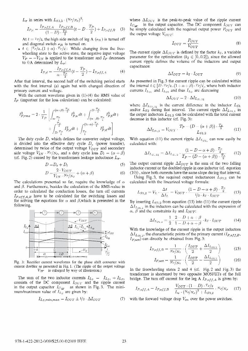
AbIOUT= k'IOUT (9)As presented in Fig. 3 the current ripple can be calculated withinthe interval t C [D TP/2.. (1 + a + 73) TP/2], where both inductorcurrents ILS1 and 'LS2 and thus ILS are decreasing
AbOUT = 2 ATILS1I21 (10)
where AIL,12, is the current difference in the inductor Ls,and/or LS2 during that interval. The current ripple AIL512 inthe output inductors LS1,2 can be calculated with the total currentdecrease in this inductor (cf. Fig. 3):
AILS12 VOUT (1 1)
With equation (11) the current ripple AIL,2, can now easily becalculated with:
(-D+a + 13). TP
ISi,21 AIS2 Tp - (D - (a /3)) .T2
(12)
The output current ripple AIOUT is the sum of the two fallinginductor current or the doubled ripple in one inductor (cf. equation(10)), since both currents have the same slope during that interval.
Using Fig. 3, the required output inductances LS1,2 can becalculated with the linearized voltage formula:
At VOUTLsli2 =VL AlLVOT (1-D+a+/3). 2I
1/2. 'i OUT(13)
By inserting LS1,2 from equation (13) into (11) the current rippleAILS12 in the inductors can be calculated with the expression ofa, 73 and the constraints k, and IOUT:
AILS12 1 2-D+a+73AI V 1 -Da7 .k1 'OUT (14)rr~k-VUWv , S s
;___
: 3-- VsVSD 2
,]<[b] >H1 [c] >[d], (calculation interval)
Fig. 3: Rectifier current waveforms for the phase shift converter withcurrent doubler as presented in Fig. 1. (The ripple of the output voltage
VcpTj is enlarged by way of illustration.)
The sum of the two inductor currents IL, = ILS1 + 'LS2consists of the DC component IOUT and the ripple currentin the output capacitor IC,, as shown in Fig. 3. The mini-mum/maximum value of ILS are given by:
ILS,min,max = IOUT ± 1/2 AIOUT (7)
With the knowledge of the current ripple in the output inductorsAILS1,2 ithe characteristic points of the primary current (IP,off,B,',act) can directly be obtained from Fig. 3:
1 (IOUT AILS12'AIP,off,B +VNp/NS \2 2
1 (IOUT AILS1 2 Alp,act = -VNp/NS \2 2/
(15)
(16)
In the freewheeling states 2 and 4 (cf. Fig. 2 and Fig. 3) thetransformer is shortened by two opposite MOSFETs of the fullbridge. The turn off current for the leg A IP,off,A is given by:
PoffA ='IP,Off,B VOUT- (1 - D)2 . T NS/NPIPoff, I ,o fB _N____Np_
La . (NsINp)2 + Lsl,2(17)
with the forward voltage drop V0, over the power switches.
978-1-422-2812-0/09/$25.00 02009 IEEE
Zz--:-AlOUT-- IL,,
"',Ls,)-t
Ti,,,
23

As depicted in Fig. 2, the primary current slope during the dutyloss time is constant and thus the quotient ajo can be expressedby 'p,act and Ip,off,A:
/3 1'P,act (18)a 1p,off,A
With the leakage inductance L¢, the applied voltage VIN and thecurrent change during the duty loss time (a + Q) TP/2, a furtherexpression for (a + Q) can be found:
+ /3= L, .1P,off,A + 'P,act (19)
Solving (18) and (19) with respect to a and Q, as well asthe equations for the characteristic primary current points andthe current ripple in the inductors (equations (17), (16), (15)and (14)), a solution for the values a, Q and thus for IP,off,A,IP,off,B and IP,act can be found. The obtained values, thecurrent waveforms are defined and all component current/voltagewaveforms can be determined in order to calculate e.g. the lossesin the semiconductors, as presented in the next subsection.
2) Semiconductor Losses: With the obtained results from theanalytical converter models the losses in the power devices (fourMOSFETs, including the antiparallel diode, and the two rectifierdiodes) can be calculated. There, the switching losses are calcu-lated based on empirical equations, determined by measurements.
With the losses, the maximum allowed junction temperaturesand the thermal resistance between junction and heat sink, thevolumes of the heat sink is calculated based on the CSPI (CoolingSystem Performance Index) [4]. It is assumed that at each point oftime one MOSFET is switched on and thus the current is carriedby the MOSFET in the inverse direction (not by the antiparalleldiodes) and therefore, the conduction losses of the MOSFETs arecalculated with the RMS-value of the primary current 'p,rms andthe MOSFET's on resistance RDS,On:
Pcond,MOS = RDS,on , rms (20)
Due to the ZVS condition the turn on losses are zero andthe turn off losses in the leg A and B are estimated based onmeasurements for the applied MOSFETs [5]:
Pzvs,off,A,B2 (1.9 'PoffAB - 38 'P,off,A,B + 140) 10 7 f (21)
if the turn off current in leg A and/or B 'P,off,A,B > 15 A. In caseof the currents 'P,off,A,B are below 15 A, the switching lossesunder ZVS-condition are negligible.
For the rectifier diodes an approximately constant forwardvoltage drop VF,rect is assumed so that the conduction lossesPcond,rect in one diode can be calculated with the averagecurrents:
Pcond,rect = VF,rect *2 (22)
Since Schottky diodes are applied, the switching losses arerelatively small and thus neglected.
For the specification of the efficiency the losses in the gatedrivers and control unit Pgate are considered as well. These lossesin the gate drives are dependent on the switching frequency andcan be calculated with the gate charge and the gate capacitance.
With the present loss equations and the analytical model ex-pressions of the currents described in before, the power loss inthe semiconductors can be calculated as:
Psemi =2 (PZVS,Off,A + PZVS,Of f,B) + 4. Pcond,MOS++ 2 * Pcond,rect + 4 Pgate
3) Outputfilter capacitors: The output filter capacitors carry-ing high frequency ripple currents with relatively high amplitudes.In order to limit the losses and the temperature rise, dielectricswith a low loss factor tan d are required. In the prototype 2.2 ,uF/ 100V / X7R ceramic capacitors in a 1210 housing from muRata[6] are utilized, which have a very high allowed ripple current pervolume ratio.From Fig. 3, the voltage over the output capacitor increases
during the charging process, i.e. when the sum of the inductorcurrents is bigger than the DC output current (IL, > IOUT). Thisis true for half of the effective duty cycle De (current increase) andhalf of effective freewheeling time (1 - De) (current decrease).Thus, the capacitance value is calculated with the currents and themaximum allowed output ripple voltage Vrippe = 300mVpp:
1(D TP )2A'1OUTCOUT tVpidKtD+PVripple L°De 2Po (I De)]tdt
2
With the currents the losses can be determined with the lossfactor and are compared with the maximum ratings from the datasheet. There, also the decrease of the capacitance with highertemperature and DC voltage is considered for the optimization.
4) Transformer Model: In the proposed optimization procedurethe shape of the transformer is optimized for minimal volumewhile keeping the hot spot temperatures below the limits. Forthis calculation the losses and the transformers temperature dis-tribution are needed as function of the geometry.
The core losses are calculated by the approach presented in [7],based on Steinmetz parameters [8] and the rate of magnetization(dB/dt). The winding losses are calculated by an ID approach,which includes skin- and proximity effect loss [9]. There, foilwindings are used which allow a better thermal management. Inorder to maximize the power density an advanced cooling methodhas been applied as described in [5]. The temperature distributionresulting from the losses can be calculated with the thermal modelof the transformer. The model describes the heat flow from thewindings/core via thermal interfaces and heat transfer componentsto the heat sinks and ambient, respectively. The transmission linebased calculation is described in detail and validated in [10].
To decrease the volume and the losses, the two output inductorsare integrated in the transformer based on a concept discussed in[11]. In the presented DC-DC converter the concept shown inFig. 4 is applied, since the flux in the center leg of the transformeris almost constant and thus the core losses are small and standardE-cores could be applied. The value of the integrated inductors isadapted by the air gap in the center leg.With the integration shown in Fig. 4 the operating behavior
of the original current doubler changes as well. In case ofthe powering state 1, there the primary current is positive, aclockwise flux is induced in the outer legs. Only in the upper
978-1-422-2812-0/09/$25.00 02009 IEEE 24

N_ NS2
Fig. 4: Integration of the Output Inductors of the Current Doubler in athe transformers core ([11])
secondary winding NS1 (cf. Fig. 4) a current flow is possible,while the current flow in lower winding NS2 is blocked by thediode D2. During the free-wheeling state 2 the primary currentIp remains positive and allows the current flow still only throughthe diode D1. During states 3 and 4 (cf. Fig. 2) the negativeprimary current Ip causes the current flow through the secondarywinding NS2. That shows a significant change: Unlike in theoriginal topology presented in Fig. lb), there the inductor currents(ILS1 and ILS2) is almost constant over a switching period, thecurrent in integrated topology flows only over one of the secondarywinding/inductor. Thus, the original name ,,current doubler"is inprinciple not entirely correct any more. However, the currentand voltage waveforms outside of the integrated transformer are
remain the same like with the original current doubler as shownin Fig. lb).
B. Comparison of Lossless Snubber Circuits
Due to a non ideal coupling coefficient between the primaryand the secondary side of the transformer, a voltage ringingoccurs across the rectifier diodes during the blocking phase. Thisringing is caused by the resonant circuit resulting from the leakageinductance L¢, the winding capacitances Cw and the diodesjunction capacitances CD (cf. Fig. Sd)). By decreasing the leakageinductance, the energy of this oscillation could be reduced, but a
minimal value of the inductance is required for ZVS switchingcondition of the MOSFETs. This effect is even enhanced forthe integrated topology because of the current shift from thefirst secondary winding (NS1) to the other (NS2). Furthermore,in order to reduce the volume of the magnetic components theswitching frequency will be increased and the winding capacitanceis relatively high since in the prototype system foil windingsare utilized, because these allow a drastically reduced thermalresistance between the winding and the heat sink. In order todecrease the occurring ringing as depicted in Fig. 6d) withoutdecreasing the efficiency, a lossless snubber circuit for the diodesis required. In Fig. 5, three possible snubber circuits are shown,which transfer a large share of the ringing energy to the output.
In Fig. 5a) a relative simple lossless snubber consisting of twoadditional diodes and one capacitor is given [12], which clampsthe voltage over the winding. After a negative voltage is appliedto primary transformer side and current in the rectifier diodes hascommutated from D1 to D2, D1 is able to absorb blocking volt-age. During the positive oscillation, the capacitor Cs, is chargedthrough the snubber diode DS1 over the transformer secondaryvoltage (VCs,max -(VINNs/NP+l/2VouT)) and the diode D1reaches the maximum blocking voltage of - (Vcsi, max + VO UT).Through the snubber diode DS2 the capacitor Cs, is dischargedby feeding the leakage energy into the output, and thereforethe oscillation is damped by the resonant charging-dischargingbehavior of the circuit. After the primary voltage changes its
D,
~ -Iar -
Fig. 5: Schematics of considered "lossless" snubber topologies for theintegrated current doubler rectifier diode: a) snubber with 2 diodes and1 capacitor (2D1C), b) snubber with 3 diodes and 2 capacitors (3D2C),c) snubber with 1 diode and damping winding. (Snubber circuit for onlyone diode is drawn for simplicity.) In d) the parasitic capacitors aredelineated which causes the current ringing other the rectifier diodes.
polarity the snubber capacitance is discharged through DS2 tooutput.An extended snubber circuit is presented in Fig. Sb), where
three diodes and two additional capacitances are applied [12],which clamp the voltage over the rectifier diode. The operatingprinciple of the different charge and discharge paths is related tothe snubber presented above (cf. Fig. Sa)): The capacitors Cs,and Cs2 are charged via DS2 for positives over voltages by theleakage energy in the transformer and discharged via DS1 andDS3. The damping to the blocking voltage level of the rectifierdiode (VD1 = -VINNs/NP) is faster but with the penalty of a
higher first voltage peak. Further information can be found in[12].
In Fig. Sc) the new circuit, which requires only a single snubberdiode DS1 and an additional small winding ND, is presented. Theidea behind this topology is getting the leakage energy directly outwith the damping winding and feed it to the output. In principle,the damping winding could also be installed on the center leg ofthe core. However, the coupling between the secondary windingsNS1,2 would be worse. The voltage over the secondary windingduring the blocking phase is transformed with the turns ratio ND:NS1,2 to the snubber diode voltage VDS12 and clamped over theoutput voltage. The maximum diode voltages VD12, can beset with the damping winding's number of turns ND:
ND = NS VOUTVD12 VOUT
(23)
With a proper choice of VD12, slightly over the steady statevoltage of VD12 the snubber diodes DS1 start conducting as soon
as VD, > VD,,max and the oscillation energy is directly fed tothe output.
Fig. 6 presents the resulting experimental damped voltages over
the rectifier diode VD1. Compared to the original curves inFig. 6d), all three snubber circuits reduces the ringing significantly.However, the best result is obtained with the new snubber circuitpresented in Fig. Sc) as shown in Fig. 6c). With this circuit thevoltage amplitude is damped by a factor of four. Especiallythe first peak is significantly reduced in comparison to the other
978-1-422-2812-0/09/$25.00 02009 IEEE
a)
c) d)
b)
25

tested lossless snubbers Fig. 5a) and b). Thus this circuit has beenimplemented in the prototype presented in section IV-A and IV-B.
Pressetting: Fixed parameters Specifications
Calculation of the operating point
d)Losses as function
of geometry
Hot spot temperature asfunction of geometry
..........................................................................................................................................
Minimization of core andheat sink volumes
Fig. 6: Measurement results of the rectifier diode voltage VD1 with thepresented snubbers a) (2D1C), b) (3DIC), c) snubber with 1 diode anddamping winding and d) without snubber circuit. The obtained voltagewithout snubber are drawn gray in a), b), and c), as well. (In order notto destroy the rectifier diodes caused by over voltage, the measurement
are taken at an input voltage VIN =20D V, 1 kW, VcT,j 35 V.)
III. POWER DENSITY OPTIMIZATION PROCEDURE
Based on the analytical models presented in the previous sectionan automatic optimization procedure has been developed forfinding the best set of converter parameters and component values,which result in a maximal power density and/or efficiency. In theproposed procedure shown in Fig. 7, all fixed electrical, thermaland magnetic components parameters and specifications are presetin the first step. These are, besides the system specifications(e.g. input/output voltage VIN/VOUT, output power POUT,ambient temperature Tamb), the characteristics of the employedcomponents, like the thermal resistances of the semiconductors,isolation materials and thermal grease as well as characteristicsof the core materials. In the next step, the free parameters likethe switching frequency, number of windings and the allowedcurrent ripple are set as initial values for the calculation. Withthe defined constraints, parameter settings and with the equationspresented in section 1I-A the operating point is calculated, whichis characterised by the duty cycle D, the duty cycle loss a + Q,the primary currents waveform characteristic IP,off,A,B/IP,j andthe output inductances LS1,2, for instance. With the calculatedoperating point, the transformer and the inductor are optimizedwith respect to power density and/or efficiency within an inneroptimization procedure, while keeping the temperatures for thecore and windings below the maximum values. Furthermore,the volume of the filter capacitors can directly be calculated andthe heat sinks determined by the losses in combination with thecooling system performance index CSPI [4]. The global opti-mization procedure changes systematically the free parameters forminimizing the overall system volume and/or efficiency. Furtherdetails are given in [5].
IV. OPTIMIZATION, CONSTRUCTION AND MEASUREMENTRESULTS
With the presented optimization procedure in section III thephase-shift converter with current doubler has been optimized for
SemicoductorFilter losses
capacitorvolurne Semicoductor
volumes
Fig. 7: Automatic procedure for optimizing the volume/efficiency ofphase-shift converter with current doubler while keeping the device
temperatures below given limits
the given specifications in table I. Amongst others, the followingcomponents/limitations have been used for calculation:
* Core material N87 from Epcos (Tmax < 115 °C)* Foil windings (Tmax < 125 °C)* Microsemi MOSFET APT5OM75* Microsemi diodes APT10OS20* Maximal junction temperature TIj,max < 140 °CThe maximum calculated power density of - 15 kW/liter.
(246W/in3) is reached at a switching frequency of - 200 kHz.There, only the net components volumes are considered sincethe final converter volumes depends strongly on the mechanicaldesign. With the prototype shown in Fig. 1 a resulting powerdensity of 9 kW/liter (147W/in3) is obtained.As presented in Fig. 8 the total volume of the converter at lower
frequencies is determined by the magnetic components in the firstplace, since the magnetic flux density is increasing but is limitedby the core materials on the one hand and the required inductanceincreases because of the increasing output current ripple on theother hand. For higher frequencies the core and winding lossesand thus the cooling volume of the magnetic components isincreasing. However, the significant rise in the volume at higherfrequencies is caused by the increasing switching losses in theMOSFETs and the increased in the required cooling volume.
With a switching frequency of approximately 200 kHz a mini-mal volume and an efficiency 94.8 % results. Mainly caused bythe lower switching losses at lower frequencies, the maximumefficiency of 95.1 % is reached around 100 kHz.
For the validation of the calculated values the resulting systemdesign has been verified by an electrical simulation in a first step.The experimental verification is realized with the prototype shownin Fig. 1. The several parts of the converter are shown in thefollowing.
A. Converter AssemblyIn Fig. 9 the sliced CAD drawing of the assembled prototype
(cf. Fig. 1) is presented. As explained in section II and depictedin Fig. 4, an integrated current doubler topology was applied. Theprimary and secondary winding are interleaved and mounted on
978-1-422-2812-0/09/$25.00 02009 IEEE
a) 2i150~
i0 l I 1I' ;
e) D~
b)
Initial Values: Set up free parameters
c5"0 1i
0
26
0,
v V.
2 4'I'inie t p s

1.5400
1.0
0.s
0
soo
400
300
200
100
tot4lT X _ / t0 ~~~~~~~~~~~~~~~~~~~~~~~..........I,LOUT heat sink othrs
trafo~30 S0 100 300 S00 10(
Frequency / [kHz]
total d
conduction (MOSFETsrect;)-..--__--- j-- __ _<_, __ _ _ _
windings switching core
)/ t- f~~z
00
30 50 100 300 50 1000Frequency f [kHz]
Fig. 8: Calculated Losses and Volumes (components housing only) forthe Current Doubler
the outer legs of an standard E-core. The spacer between theprimary and secondary/damping winding determines the necessaryleakage inductance for the soft switching. The heat is extracted outof the core and the winding by the heat transfer components whichare ending in the transformer heat sink. The airflow is forced by ahigh performance fan from the rectifier side (left) to the MOSFET'sside. The energy is transferred by low inductive connectorsto the output and input board. Due to the applied bootstraptopology, the digital control, gate driver and control supply couldbe implemented on one single PCB (90mm x 40mm) in front ofthe converter system. Further details are presented in Fig. 9 or theprototype in Fig. 1.
Fig. 9: Drawing of the prototype with a cut through the transformer heatsink and winding. (The upper cover have been omitted.)
B. Measurement Results
For the validation of the calculation and simulation results,thermal and electrical measurements have been performed withthe presented prototype. The results are shown for the inter-leg voltage VAB and the rectifier voltage VD1 in Fig. 10. Dueto the zero voltage switching, VAB shows no voltage ringing atfull power and the rectifier diodes voltage ringing is drasticallydecreased to secured operation area. The measured efficiency atfull power is 94.75 % and agrees very well with the theoreticalcalculations. Furthermore, the thermal design could be validatedthrough IR temperature measurements.
4Time t [us]
Fig. 10: Measured Curves: Primary Voltage Vc and Rectifier DiodeVoltage VD1 at 5 kW Output Power
V. CONCLUSION
In this paper a power-density-optimized 400 V/48..56V telecomphase-shift DC-DC converter with an integrated current doublerrectifier and 5 kW output power is presented. For the opti-mization a procedure, based on comprehensive analytical modelsof the converter including magnetic components and thermalmanagement, is applied to determine the component values ofthe converter. After verifying the resulting parameters by anelectrical simulation, a prototype has been constructed, which hasa power density of 9 kW/liter (147W/in3) and integrates the outputinductors in the transformer. With this prototype measurementsare performed for validating the analytical calculations.
Furthermore, a new snubber circuit for the rectifier diodes,which performs an almost lossless damping of the diode voltageis presented and validated by measurements.
REFERENCES[1] J. W. Kolar, U. Drofenik, J. Biela, M. L. Heldwein, H. Ertl, T. Friedli, and
S. D. Round, "PWM converter power density barriers," in Proceedings ofthe 4th Power Conversion Conference (PCC'07), apr 2007.
[2] J. W. Kolar, J. Biela, and U. Badstuebner, "Impact of power density maxi-mization on efficiency of dc-dc converter systems," in The 7th InternationalConference on Power Electronics (ICPE'07), oct 2007.
[3] B. R. Lin, K. Huang, and D. Wang, "Analysis and implementation of full-bridge converter with current doubler rectifier," in IEE Proceedings ElectricPower Applications, vol. 152, no. 5, sep 2005, pp. 1193-1202.
[4] U. Drofenik, G. Laimer, and J. W. Kolar, "Theoretical converter power den-sity limits for forced convection cooling," in Proceedings of the InternationalPCIM'05 Europe Conference, jun 2005, pp. 608-619.
[5] J. Biela, U. Badstuebner, and J. W. Kolar, "Design of a 5kw, 1 u, 10 kw/ltrresonant dc-dc converter for telecomapplications," in 29th InternationalTelecommunications Energy Conference (INTELEC'07), sep 2007.
[6] "Homepage of murata manufacturing co., ltd." [Online]. Available:http://www.murata.com/
[7] K. Venkatachalam, S. C. R., T. Abdallah, and H. Tacca, "Accurate predictionof ferrite core loss with nonsinusoidal waveforms using only steinmetzparameters," in IEEE Workshop on Computers in Power Electronics, 3-4June 2002, pp. 36-41.
[8] C. P. Steinmetz, "On the law of hysteresis," in Proceedings of the IEEE,vol. 72, feb 1984, pp. 197 - 221.
[9] W. G. Hurley, E. Gath, and J. G. Breslin, "Optimizing the ac resistance ofmultilayer transformer windings with arbitrary current waveforms," in IEEETransactions on Power Electronics, vol. 15, mar 2000, pp. 369 - 376.
[10] J. Biela and J. W. Kolar, "Cooling concepts for high power density magneticdevices," in Proceedings of the 4th Power Conversion Conference (PCC'07),apr 2007.
[11] X. Peng, W. Qiaoqiao, W. Pit-Leong, and F. C. Lee, "A novel integrated cur-rent doubler rectifier," in Fifteenth Annual IEEE Applied Power ElectronicsConference and Exposition (APEC'00), vol. 2, feb 2000, pp. 735 - 740.
[12] H. Mao, J. A. Abu-Qahouq, W. Qiu, Y. Wen, and I. Batarseh, "Losslesssnubber circuits for current doubler rectifiers to reduce reverse-recoverylosses," in The 29th Annual Conference of the IEEE Industrial ElectronicsSociety (IECON '03), vol. 3, 2-6 Nov. 2003, pp. 2639-2644Vol.3.
978-1-422-2812-0/09/$25.00 02009 IEEE 27