Embed Size (px)
Citation preview
Al-Ameri, Talib (2018) Modelling and simulation study of NMOS Si
nanowire transistors. PhD thesis.
https://theses.gla.ac.uk/30651/
Copyright and moral rights for this work are retained by the author
A copy can be downloaded for personal non-commercial research or study,
without prior permission or charge
This work cannot be reproduced or quoted extensively from without first
obtaining permission in writing from the author
The content must not be changed in any way or sold commercially in any
format or medium without the formal permission of the author
When referring to this work, full bibliographic details including the author,
title, awarding institution and date of the thesis must be given
Enlighten: Theses
https://theses.gla.ac.uk/
Modelling and Simulation Study of
NMOS Si Nanowire Transistors
Talib Al-Ameri
BSc. MSc. PhD. Electronics Engineering
School of Engineering
University of Glasgow
June 2018

I
Dedication
To my brave sons Mustafa and Ali
II
Abstract
Nanowire transistors (NWTs) represent a potential alternative to Silicon FinFET technology
in the 5nm CMOS technology generation and beyond. Their gate length can be scaled
beyond the limitations of FinFET gate length scaling to maintain superior off-state leakage
current and performance thanks to better electrostatic control through the semiconductor
nanowire channels by gate-all-around (GAA) architecture. Furthermore, it is possible to
stack nanowires to enhance the drive current per footprint. Based on these considerations,
vertically-stacked lateral NWTs have been included in the latest edition of the International
Technology Roadmap for Semiconductors (ITRS) to allow for further performance
enhancement and gate pitch scaling, which are key criteria of merit for the new CMOS
technology generation. However, electrostatic confinement and the transport behaviour in
these devices are more complex, especially in or beyond the 5nm CMOS technology
generation.
At the heart of this thesis is the model-based research of aggressively-scaled NWTs suitable
for implementation in or beyond the 5nm CMOS technology generation, including their
physical and operational limitations and intrinsic parameter fluctuations. The Ensemble
Monte Carlo approach with Poisson-Schrödinger (PS) quantum corrections was adopted for
the purpose of predictive performance evaluation of NWTs. The ratio of the major to the
minor ellipsoidal cross-section axis (cross-sectional aspect ratio - AR) has been identified
as a significant contributing factor in device performance. Until now, semiconductor
industry players have carried out experimental research on NWTs with two different cross-
sections: circular cylinder (or elliptical) NWTs and nanosheet (or nanoslab) NWTs. Each
version has its own benefits and drawbacks; however, the key difference between these two
versions is the cross-sectional AR. Several critical design questions, including the optimal
NWT cross-sectional aspect ratio, remain unanswered. To answer these questions, the AR
of a GAA NWT has been investigated in detail in this research maintaining the cross-
sectional area constant. Signatures of isotropic charge distributions within Si NWTs were
III
observed, exhibiting the same attributes as the golden ratio (Phi), the significance of which
is well-known in the fields of art and architecture.
To address the gap in the existing literature, which largely explores NWT scaling using
single-channel simulation, thorough simulations of multiple channels vertically-stacked
NWTs have been carried out with different cross-sectional shapes and channel lengths.
Contact resistance, non-equilibrium transport and quantum confinement effects have been
taken into account during the simulations in order to realistically access performance and
scalability.
Finally, the individual and combined effects of key statistical variability (SV) sources on
threshold voltage (VT), subthreshold slope (SS), ON-current (Ion) and drain-induced barrier
lowering (DIBL) have been simulated and discussed. The results indicate that the variability
of NWTs is impacted by device architecture and dimensions, with a significant reduction in
SV found in NWTs with optimal aspect ratios. Furthermore, a reduction in the variability of
the threshold voltage has been observed in vertically-stacked NWTs due to the cancelling-
out of variability in double and triple lateral channel NWTs.
IV
Acknowledgements
Thanks be to Allah, Almighty, for giving me the strength to complete this study.
My deepest gratitude to my principal supervisor Professor Asen Asenov for his patience,
support, dedication and guidance in all the stages of this study. I would like to thank my
second supervisor, Dr Vihar Georgiev, for his valuable comments, reading, exchanges of
ideas, and support. He has been on hand to answer the many questions I've asked during my
study. Also, I would like to thank Dr Fikru for the technical discussions and help.
I am also thankful to Prof Andy Knox, Prof Ravinder Dahiya, and Dr Edward Wasige
(University of Glasgow) for their valuable comments during the annual reviews.
Thanks also go to Synopsis engineers (the former members of The Glasgow device
modelling group): Dr Craig Alexander, Dr Salvatore Amoroso, Dr Craig Riddet, Dr Ewan
Towie, and Andrew Brown. They also answered the many questions I had about statistical
variability, Poisson-Schrödinger and Monte Carlo simulations. I am grateful to Dr Gordon
Stewart and Engineer Grant Quinn, whose IT knowledge was a resource I tapped into
numerous times.
I am also grateful to CEA-Leti for the training course "Reliability & Defects in Advanced
CMOS Technologies".
My deepest gratitude and appreciation also go to my financial sponsor the Ministry of Higher
Education and Scientific Research, Iraq and Al-Mustansiriyha University for nominating me
to study abroad and funding my scholarship.
An important thank you goes to my parents without whose unlimited love and contributions,
I would not have been able to complete this study.
I would also like to thank my wife for her endless inspiration and support and my lovely,
brave sons Mustafa and Ali, who missed their dad for a long time.
During my PhD journey, I met many people in Glasgow who participated in the success of
this study. Thank you to all of you.
Thank you,
V
Author's Declaration
I declare that, except where explicit reference is made to the contribution of others, that this
thesis is the result of my own work and has not been submitted for any other degree at the
University of Glasgow or any other institution.
Signature
Talib Mahmood Ali Al-Ameri
June 2018
VI
Publications
1. Al-Ameri T, Georgiev VP, Adamu-Lema F, Asenov A. Simulation Study of Vertically Stacked
Lateral Si Nanowires Transistors for 5-nm CMOS Applications. IEEE J Electron Devices Soc.
2017;5(6):466-472. doi:10.1109/JEDS.2017.2752465.
2. Al-Ameri T, Georgiev VP, Sadi T, et al. Impact of quantum confinement on transport and the
electrostatic driven performance of silicon nanowire transistors at the scaling limit. Solid State
Electron. 2017;129:73-80. doi:10.1016/j.sse.2016.12.015.
3. Al-Ameri T. Correlation between the Golden Ratio and Nanowire Transistor Performance. Appl
Sci. 2018;8(1):54. doi:10.3390/app8010054.
4. Wang Y, Al-Ameri T, Wang X, et al. Simulation Study of the Impact of Quantum Confinement
on the Electrostatically Driven Performance of n-type Nanowire Transistors. IEEE Trans. Electron
Devices. 2015;62(10):3229-3236. doi:10.1109/TED.2015.2470235.
5. Georgiev VP, Amoroso SM, Talib M A, et al. Comparison Between Bulk and FDSOI POM Flash
Cell: A Multiscale Simulation Study. IEEE Trans Electron Devices. 2015;62(2):680-684.
doi:10.1109/TED.2014.2378378.
6. Al-Ameri T, Georgiev VP, Adamu-Lema F, Asenov A. Does a nanowire transistor follow the
golden ratio? A 2D Poisson-Schrödinger/3D Monte Carlo simulation study. In: 2017 International
Conference on Simulation of Semiconductor Processes and Devices (SISPAD). IEEE; 2017:57-60.
doi:10.23919/SISPAD.2017.8085263.
7. Al-Ameri T, Georgiev VP, Adamu-Lema F, et al. Impact of strain on the performance of Si
nanowires transistors at the scaling limit: A 3D Monte Carlo/2D Poisson Schrodinger simulation
study. In: 2016 International Conference on Simulation of Semiconductor Processes and Devices
(SISPAD). IEEE; 2016:213-216. doi:10.1109/SISPAD.2016.7605185.
VII
8. Al-Ameri T, Georgiev VP, Lema FA, et al. Performance of vertically stacked horizontal Si
nanowires transistors: A 3D Monte Carlo/2D Poisson Schrodinger simulation study. In: 2016 IEEE
Nanotechnology Materials and Devices Conference (NMDC). IEEE; 2016:1-2.
doi:10.1109/NMDC.2016.7777117.
9. Al-Ameri T, Asenov A. Vertically stacked lateral Si80Ge20 nanowires transistors for 5 nm CMOS
applications. In: 2017 Joint International EUROSOI Workshop and International Conference on
Ultimate Integration on Silicon (EUROSOI-ULIS). Athens: IEEE; 2017:101-104.
doi:10.1109/ULIS.2017.7962612.
10. Al-Ameri T, Wang Y, Georgiev VP, Adamu-Lema F, Wang X, Asenov A. Correlation between gate
length, geometry and electrostatic driven performance in ultra-scaled silicon nanowire transistors.
In: 2015 IEEE Nanotechnology Materials and Devices Conference (NMDC). IEEE; 2015:1-5.
doi:10.1109/NMDC.2015.7439240.
11. Al-Ameri T, Georgiev VP, Adamu-Lema F, Wang X, Asenov A. Influence of quantum
confinement effects and device electrostatic driven performance in ultra-scaled SixGe1−x nanowire
transistors. In: 2016 Joint International EUROSOI Workshop and International Conference on
Ultimate Integration on Silicon (EUROSOI-ULIS). IEEE; 2016:234-237.
doi:10.1109/ULIS.2016.7440096.
12. Al-Ameri T. Vertically Stacked Lateral Nanowire Transistors: Optimisation for 5nm CMOS
Technology. In: 2017 IEEE Nanotechnology Materials and Devices Conference (NMDC). IEEE;
2017:1-3. http://eprints.gla.ac.uk/149995/.
13. Al-Ameri, T., Georgiev, V.P., Adamu-Lema, F. and Asenov, A. (2017) Variability-Aware
Simulations of 5 nm Vertically Stacked Lateral Si Nanowires Transistors. International Workshop on
Computational Nanotechnology, Windermere, UK, 2017. http://eprints.gla.ac.uk/149648/
14. Al-Ameri T. Statistical Variability in 5 nm Vertically Stacked Lateral Si Nanowire Transistors. In:
2017 IEEE Nanotechnology Materials and Devices Conference (NMDC). IEEE; 2017.
http://eprints.gla.ac.uk/149994/.
VIII
15. Al-Ameri, T., Georgiev, V.P., Adamu-Lema, F. and Asenov, A. (2017) Position-Dependent
Performance in 5 nm Vertically Stacked Lateral Si Nanowires Transistors. International Workshop
on Computational Nanotechnology, Windermere, UK, 2017. http://eprints.gla.ac.uk/149647/
16. Georgiev VP, Talib M Ali, Wang Y, Gerrer L, Amoroso SM, Asenov A. Influence of quantum
confinement effects over device performance in circular and elliptical silicon nanowire transistors.
In: 2015 International Workshop on Computational Electronics (IWCE). IEEE; 2015:1-4.
doi:10.1109/IWCE.2015.7301960.
17. Adamu-Lema F, Duan M, Berrada S, J Lee, T Al-Ameri, et al. (Invited) Modelling and Simulation
of Advanced Semiconductor Devices. ECS Trans. 2017;80(4):33-42. doi:10.1149/08004.0033ecst.
18. Asenov A, Wang Y, Cheng B, X Wang, P Asenov, T Al-Ameri, et al. Nanowire transistor solutions
for 5nm and beyond. In: 2016 17th International Symposium on Quality Electronic Design (ISQED).
IEEE; 2016:269-274. doi:10.1109/ISQED.2016.7479212.
IX
Participations
I. Contributing as a reviewer for 7 journals (2017-2018):
• IEEE Transactions on Electron Devices.
• IEEE Journal of the Electron Devices Society.
• Applied Sciences (MDPI).
• Journal of Computational Electronics (Springer).
• Materials (MDPI).
• Electronics (MDPI).
• IEEE Transactions on Nanotechnology.
https://publons.com/author/983777/talib-al-ameri#profile
II. Participating in Technical Program Committee (TPC) for the 13th IEEE
Nanotechnology Materials and Devices Conference (NMDC 2018, USA).
III. CEA-Leti training course (Reliability & Defects in Advanced CMOS Technologies),
2018, France.

X
Nomenclatures and Acronyms
1D One dimension
2D Two dimensions
3D Three dimensions
CMOS Complementary Metal Oxide Semiconductor
DD Drift-Diffusion
DG Density Gradient
DIBL Drain Induced Barrier Lowering
EOT Equivalent Oxide Thickness
FDUTB Fully Depleted Ultra-Thin Body
FinFET Fin Field Effect Transistor
GAA Gate All Around
GSS Gold Standard Simulations
IC Integrated Circuit
ITRS International Technology Roadmap for Semiconductors
Ion On-current
Ioff Leakage current
Lg Gate length
Ls Spacer length
N Doping concentration
R Contact resistance
Si Silicon
SiO2 Silicon dioxide
Si3N4 Silicon oxynitride
Tox Gate dielectric thickness
T Temperature
TSi Silicon body thickness
VDD Supply voltage
VD Drain voltage
VT Threshold voltage
WF Work function
α Scaling factor
E Electric field
µ Carrier mobility
ơVT Threshold voltage standard deviation
ơIon On-current standard deviation
ơDIBL DIBL standard deviation
LER Line Edge Roughness
MC Monte Carlo
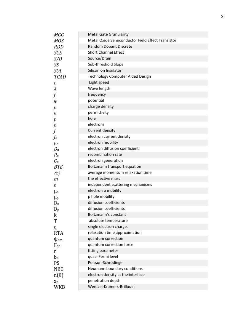
XI
MGG Metal Gate Granularity
MOS Metal Oxide Semiconductor Field Effect Transistor
RDD Random Dopant Discrete
SCE Short Channel Effect
S/D Source/Drain
SS Sub-threshold Slope
SOI Silicon on Insulator
TCAD Technology Computer Aided Design
c Light speed
λ Wave length
f frequency
ψ potential
ρ charge density
ϵ permittivity
p hole
n electrons
J Current density
Jn electron current density
μn electron mobility
Dn electron diffusion coefficient
Rn recombination rate
Gn electron generation
BTE Boltzmann transport equation
⟨τ⟩ average momentum relaxation time
m the effective mass
n independent scattering mechanisms
μn electron p mobility
μp p hole mobility
Dn diffusion coefficients
Dp diffusion coefficients
k Boltzmann’s constant
T absolute temperature
q single electron charge.
RTA relaxation time approximation
ψqm quantum correction
Fqc quantum correction force
r fitting parameter
bn quasi-Fermi level
PS Poisson-Schrödinger
NBC Neumann boundary conditions
n(0) electron density at the interface
xp penetration depth
WKB Wentzel-Kramers-Brillouin

XII
mox oxide’s electron effective mass
ΦB oxide’s potential
SOR successive over relaxation
BICGSTAB biconjugate gradient-stable
rc cut-off radius
μ⊥ perpendicular field-dependent mobility
Ec critical electric field
α secondary fitting parameter
SG Gaussian autocorrelation function
(H (x)) real height function
σ standard deviation
XIII
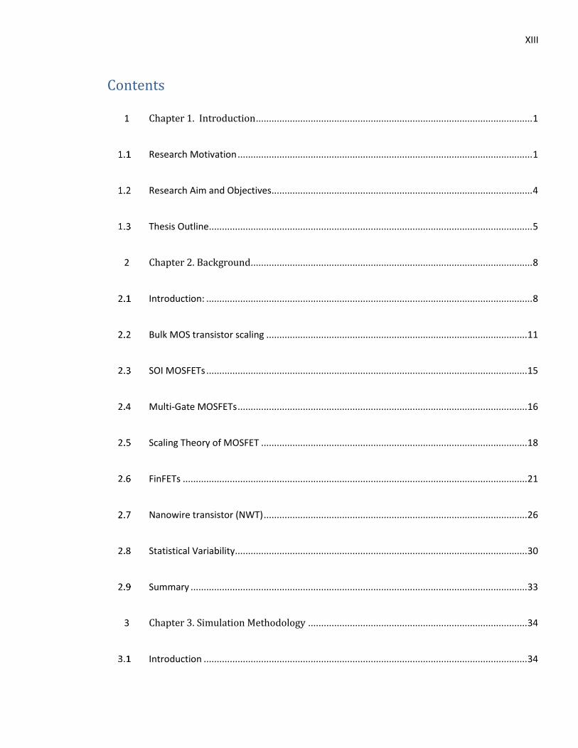
Contents
1 Chapter 1. Introduction .......................................................................................................... 1
Research Motivation ................................................................................................................. 1
Research Aim and Objectives .................................................................................................... 4
Thesis Outline ............................................................................................................................ 5
2 Chapter 2. Background ............................................................................................................ 8
Introduction: ............................................................................................................................. 8
Bulk MOS transistor scaling .................................................................................................... 11
SOI MOSFETs ........................................................................................................................... 15
Multi-Gate MOSFETs ............................................................................................................... 16
Scaling Theory of MOSFET ...................................................................................................... 18
FinFETs .................................................................................................................................... 21
Nanowire transistor (NWT) ..................................................................................................... 26
Statistical Variability ................................................................................................................ 30
Summary ................................................................................................................................. 33
3 Chapter 3. Simulation Methodology .................................................................................... 34
Introduction ............................................................................................................................ 34
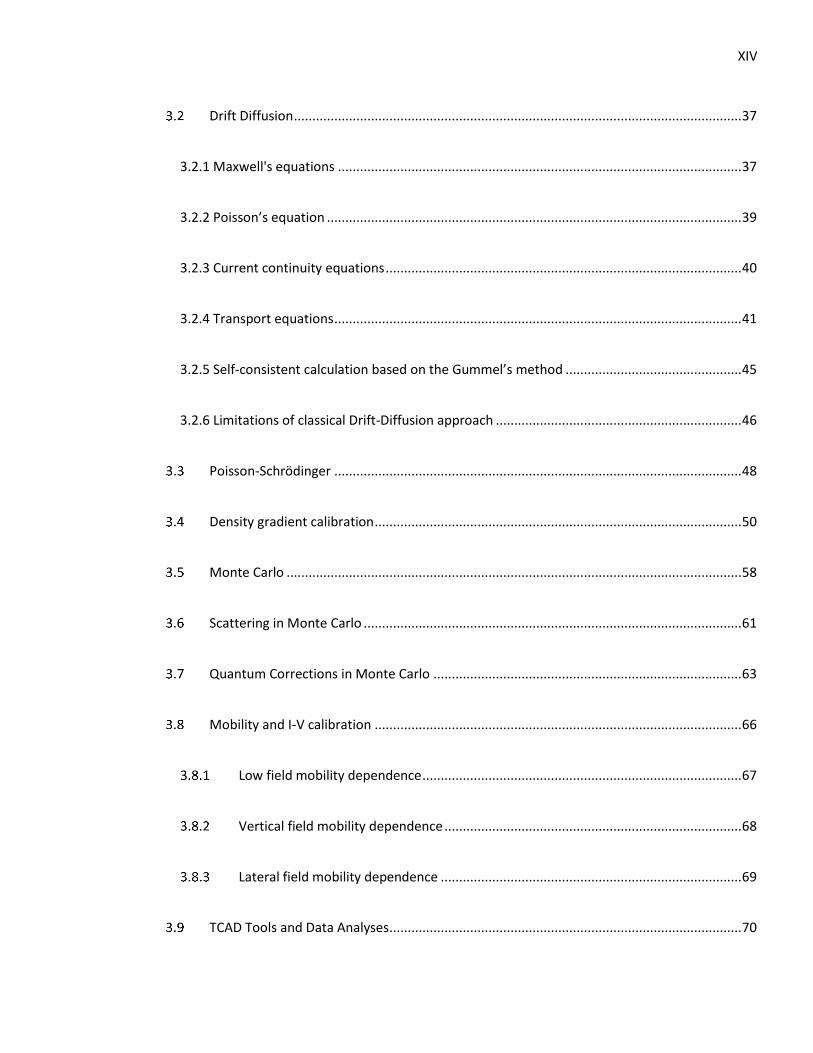
XIV
Drift Diffusion .......................................................................................................................... 37
3.2.1 Maxwell's equations .............................................................................................................. 37
3.2.2 Poisson’s equation ................................................................................................................. 39
3.2.3 Current continuity equations ................................................................................................. 40
3.2.4 Transport equations ............................................................................................................... 41
3.2.5 Self-consistent calculation based on the Gummel’s method ................................................ 45
3.2.6 Limitations of classical Drift-Diffusion approach ................................................................... 46
Poisson-Schrödinger ............................................................................................................... 48
Density gradient calibration .................................................................................................... 50
Monte Carlo ............................................................................................................................ 58
Scattering in Monte Carlo ....................................................................................................... 61
Quantum Corrections in Monte Carlo .................................................................................... 63
Mobility and I-V calibration .................................................................................................... 66
Low field mobility dependence ....................................................................................... 67
Vertical field mobility dependence ................................................................................. 68
Lateral field mobility dependence .................................................................................. 69
TCAD Tools and Data Analyses ................................................................................................ 70
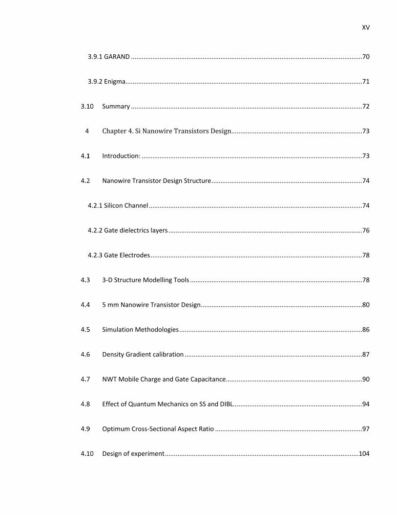
XV
3.9.1 GARAND ................................................................................................................................. 70
3.9.2 Enigma .................................................................................................................................... 71
Summary ................................................................................................................................. 72
4 Chapter 4. Si Nanowire Transistors Design......................................................................... 73
Introduction: ........................................................................................................................... 73
Nanowire Transistor Design Structure .................................................................................... 74
4.2.1 Silicon Channel ....................................................................................................................... 74
4.2.2 Gate dielectrics layers ............................................................................................................ 76
4.2.3 Gate Electrodes ...................................................................................................................... 78
3-D Structure Modelling Tools ................................................................................................ 78
5 mm Nanowire Transistor Design .......................................................................................... 80
Simulation Methodologies ...................................................................................................... 86
Density Gradient calibration ................................................................................................... 87
NWT Mobile Charge and Gate Capacitance ............................................................................ 90
Effect of Quantum Mechanics on SS and DIBL........................................................................ 94
Optimum Cross-Sectional Aspect Ratio .................................................................................. 97
Design of experiment ............................................................................................................ 104
XVI
Conclusions ........................................................................................................................... 106
5 Chapter 5. Performance of Si NWTs .................................................................................. 107
Introduction: ......................................................................................................................... 107
Device Description: ............................................................................................................... 110
Ensemble Monte Carlo (EMC) Simulation: ........................................................................... 110
Drift Diffusion Calibration ..................................................................................................... 113
5nm NWT: MC simulation ..................................................................................................... 115
Strain and channel orientation effects ................................................................................. 116
Vertically stacked lateral NWT .............................................................................................. 122
Source/drain contact resistance ........................................................................................... 124
Current density: series resistance effect .............................................................................. 125
Single-, double- and triple-channel NWT capacitance .......................................................... 130
Optimization of 5 nm NWT ................................................................................................... 131
Summary ............................................................................................................................... 135
6 Chapter 6. Study of statistical variability........................................................................... 136
Introduction .......................................................................................................................... 136
Variability sources ................................................................................................................. 138
XVII
Random discrete dopants (RDD) ........................................................................................... 138
Line edge roughness (LER) .................................................................................................... 144
Metal gate granularity (MGG) ............................................................................................... 148
SV combinations ................................................................................................................... 150
Cross-sectional aspect ratio improves SV ............................................................................. 157
Statistical variability of stacked NWT .................................................................................... 158
Additional variability sources ................................................................................................ 163
Summary ............................................................................................................................... 163
7 Chapter 7. Conclusions and Future work .......................................................................... 164
Conclusions ........................................................................................................................... 164
Contributions ........................................................................................................................ 167
Recommendations ................................................................................................................ 170
8 References ............................................................................................................................ 172
XVIII
List of figures
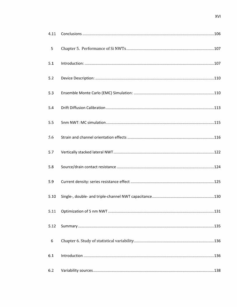
Figure 2-1 Moore’s Law with regard to count of transistors and year of introductions [19]. ................................ 10
Figure 2-2 Moore’s Law with regard to the number of transistors of transistors in Intel’s microprocessors [19-21].
....................................................................................................................................................................... 10
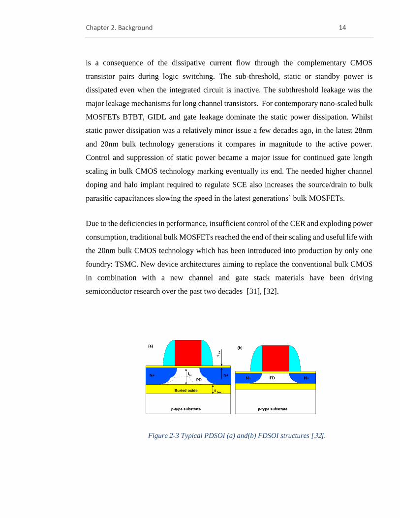
Figure 2-3 Typical PDSOI (a) and(b) FDSOI structures [32]. .............................................................................. 14
Figure 2-4 Double gate FET transistor structure to improve performance whilst reducing Ioff. (a) double gate FET
with a channel in the plane of the wafer, with the first gate over it and the second gate beneath. The channel
is vertical on the wafer’s surface with one gate on each side (b) and (c). Two structures of the vertical channel
have the current direction parallel to the FinFET (b), or parallel to the wafer surface (c)[64]. .................... 17
Figure 2-5 Three-dimensional schematic representation for the SOI and bulk FinFET. ........................................ 22
Figure 2-6 Three-dimensional schematic representation for the SOI FinFET. The fin diverges from the vertical by
8o [73]. ........................................................................................................................................................... 23
Figure 2-7 Impact of fin width on FinFET Ion/Ioff performance. TCAD simulations have been shown that DIBL, SS,
and gate length (LG) are optimised at Wc≈4nm. This critical fin width has been selected as reference point
refer to (100% performance). Here, performance Ion/Ioff is improved as the fin width is scaled up to 5.5nm but
deteriorates swiftly with fin width [81]. ....................................................................................................... 25
Figure 2-8 A Uniform NWT with four elliptical cross-sections (18.8nm×20.2nm), (16.5nm×13.8nm),
(10.2nm×10.6nm), and (6.3nm×5.0nm) [82]. ............................................................................................... 27
Figure 2-9 2D-Cross-section of a FinFET, vertically-stacked lateral NWTs and stacked Nanosheets. ................. 29
Figure 2-10 Schematics of vertical NWTs with an array of 3×3 NWTs. ............................................................... 30
Figure 2-11 The main statistical variability sources (RDD, MGG, and LER) in Si NWT. .................................... 32
Figure 3-2 The calibration flow chart of DD to quantum corrected 3D Monte Carlo simulation.
XIX
Figure 3-1 The calibration flow chart of DD to Poisson-Schrödinger simulation. ......
Figure 3-3 Simulation flowchart for Drift Diffusion based a modified Gummel algorithm [8]. ............................ 55
Figure 3-4 Flow Diagram of the 2D Poisson-Schrödinger model [8]. ................................................................... 56
Figure 3-5 Flow diagram of the fixed Schrödinger quantum correction DD model [8]. ........................................ 57
Figure 3-6 Flowchart showing the computational steps needed for Self-Consistent Quantum Monte Carlo [120].
....................................................................................................................................................................... 60
Figure 3-7 Flow diagram defining the relation between the GARAND drift-diffusion and Monte Carlo simulation
modules. ........................................................................................................................................................ 71
Figure 4-1 schematic view and material details of the circular NWT (S/D contacts are not shown). .................... 75
Figure 4-2 Process flow of (Sigmund) strector editor. ......................................................................................... 79
Figure 4-3 A 3D representation of cylindrical NWTs with S/D contacts. .............................................................. 82
Figure 4-4 The doping profile of the Si NWT with gate length Lg12 nm and spacer length Ls=5nm. .................. 83
Figure 4-5 Wave functions in the Δ1, Δ2, Δ3, and Δ4 degenerate valleys in the perpendicular (slice) cross-section
of Si NWT(PS simulation). ........................................................................................................................... 84
Figure 4-6 Four NWT’s cross-sections simulated in this subsection. Comparison of the charge distribution in the
NWT cross-section obtained from three simulations methods; Poisson-Schrödinger, density gradient the
classical DD. The simulations at low drain voltage and at gate voltage VG=0.60V. ..................................... 85
Figure 4-7 Charge distributions obtained from the standard DG and calibrated DG of Si NWT cross-sections. .. 88
Figure 4-8 Capacitance-voltage (C-V) characteristics of the simulated NWT with six different cross-sections. .. 89
Figure 4-9 1D charge distributions obtained from the PS simulation and DG simulation. The cutline is along of
perpendicular ‘diameters’ (y and z) of the NWT’s slice at the mid of the gate. ............................................ 89
XX
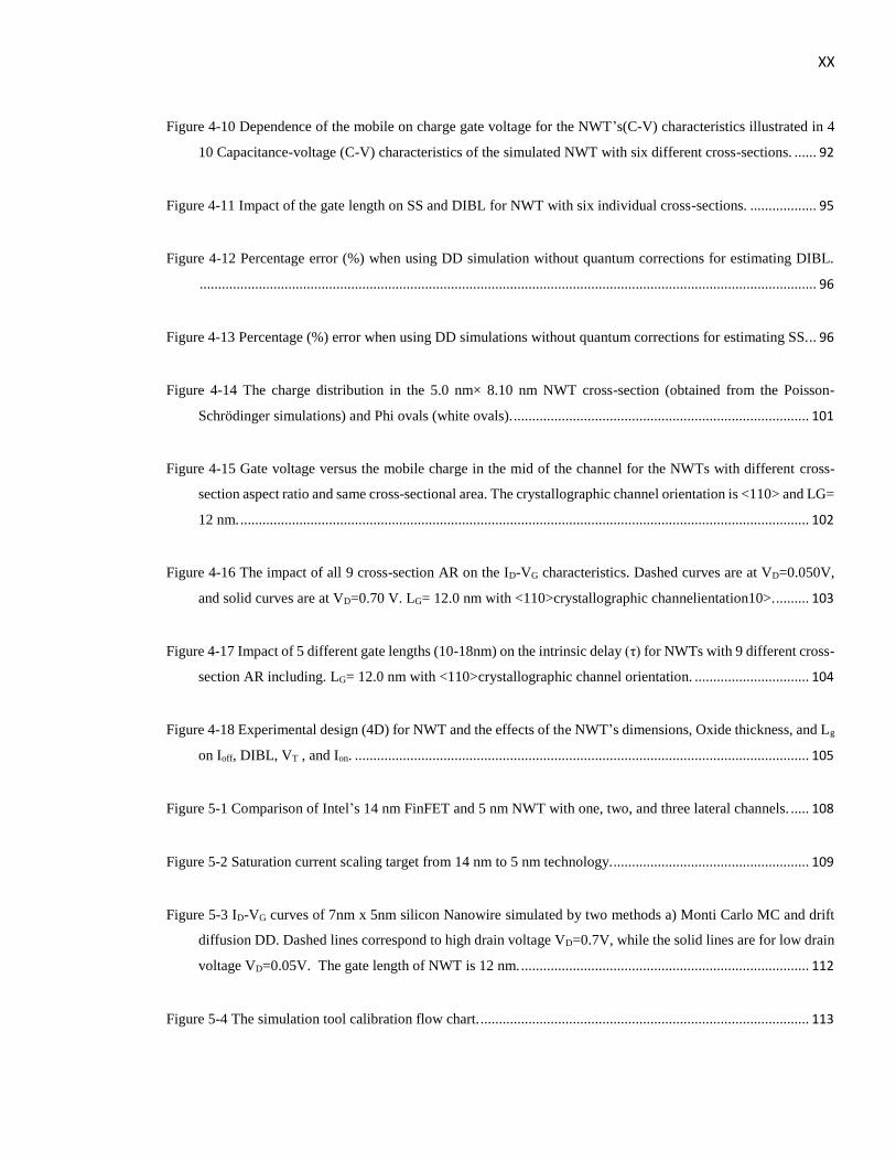
Figure 4-10 Dependence of the mobile on charge gate voltage for the NWT’s(C-V) characteristics illustrated in 4
10 Capacitance-voltage (C-V) characteristics of the simulated NWT with six different cross-sections. ...... 92
Figure 4-11 Impact of the gate length on SS and DIBL for NWT with six individual cross-sections. .................. 95
Figure 4-12 Percentage error (%) when using DD simulation without quantum corrections for estimating DIBL.
....................................................................................................................................................................... 96
Figure 4-13 Percentage (%) error when using DD simulations without quantum corrections for estimating SS... 96
Figure 4-14 The charge distribution in the 5.0 nm× 8.10 nm NWT cross-section (obtained from the Poisson-
Schrödinger simulations) and Phi ovals (white ovals). ................................................................................ 101
Figure 4-15 Gate voltage versus the mobile charge in the mid of the channel for the NWTs with different cross-
section aspect ratio and same cross-sectional area. The crystallographic channel orientation is <110> and LG=
12 nm. .......................................................................................................................................................... 102
Figure 4-16 The impact of all 9 cross-section AR on the ID-VG characteristics. Dashed curves are at VD=0.050V,
and solid curves are at VD=0.70 V. LG= 12.0 nm with <110>crystallographic channelientation10>. ......... 103
Figure 4-17 Impact of 5 different gate lengths (10-18nm) on the intrinsic delay (τ) for NWTs with 9 different cross-
section AR including. LG= 12.0 nm with <110>crystallographic channel orientation. ............................... 104
Figure 4-18 Experimental design (4D) for NWT and the effects of the NWT’s dimensions, Oxide thickness, and Lg
on Ioff, DIBL, VT , and Ion. ........................................................................................................................... 105
Figure 5-1 Comparison of Intel’s 14 nm FinFET and 5 nm NWT with one, two, and three lateral channels. ..... 108
Figure 5-2 Saturation current scaling target from 14 nm to 5 nm technology. ..................................................... 109
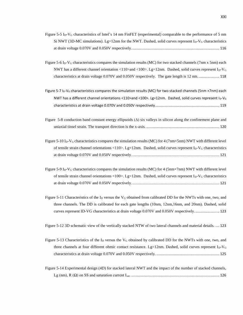
Figure 5-3 ID-VG curves of 7nm x 5nm silicon Nanowire simulated by two methods a) Monti Carlo MC and drift
diffusion DD. Dashed lines correspond to high drain voltage VD=0.7V, while the solid lines are for low drain
voltage VD=0.05V. The gate length of NWT is 12 nm. .............................................................................. 112
Figure 5-4 The simulation tool calibration flow chart. ......................................................................................... 113
XXI
Figure 5-5 ID-VG characteristics of Intel’s 14 nm FinFET (experimental) comparable to the performance of 5 nm
Si NWT (3D-MC simulations). Lg=12nm for the NWT. Dashed, solid curves represent ID-VG characteristics
at drain voltage 0.070V and 0.050V respectively. ....................................................................................... 116
Figure 5-6 ID-VG characteristics compares the simulation results (MC) for two stacked channels (7nm x 5nm) each
NWT has a different channel orientation <110>and <100>. Lg=12nm. Dashed, solid curves represent ID-VG
characteristics at drain voltage 0.070V and 0.050V respectively. The gate length is 12 nm. ..................... 118
Figure 5-7 ID-VG characteristics compares the simulation results (MC) for two stacked channels (5nm ×7nm) each
NWT has a different channel orientations <110>and <100>. Lg=12nm. Dashed, solid curves represent ID-VG
characteristics at drain voltage 0.070V and 0.050V respectively. ............................................................... 119
Figure 5-8 conduction band constant energy ellipsoids (Δ) six valleys in silicon along the confinement plane and
uniaxial tinsel strain. The transport direction is the x-axis. ......................................................................... 120
Figure 5-10 ID-VG characteristics compares the simulation results (MC) for 4 (7nm×5nm) NWT with different level
of tensile strain channel orientations <110>. Lg=12nm. Dashed, solid curves represent ID-VG characteristics
at drain voltage 0.070V and 0.050V respectively. ....................................................................................... 121
Figure 5-9 ID-VG characteristics compares the simulation results (MC) for 4 (5nm×7nm) NWT with different level
of tensile strain channel orientations <100>. Lg=12nm. Dashed, solid curves represent ID-VG characteristics
at drain voltage 0.070V and 0.050V respectively. ....................................................................................... 121
Figure 5-11 Characteristics of the ID versus the VG obtained from calibrated DD for the NWTs with one, two, and
three channels. The DD is calibrated for each gate lengths (10nm, 12nm,16nm, and 20nm). Dashed, solid
curves represent ID-VG characteristics at drain voltage 0.070V and 0.050V respectively. ........................ 123
Figure 5-12 3D schematic view of the vertically stacked NTW of two lateral channels and material details. .... 123
Figure 5-13 Characteristics of the ID versus the VG obtained by calibrated DD for the NWTs with one, two, and
three channels at four different ohmic contact resistance. Lg=12nm. Dashed, solid curves represent ID-VG
characteristics at drain voltage 0.070V and 0.050V respectively. ............................................................... 125
Figure 5-14 Experimental design (4D) for stacked lateral NWT and the impact of the number of stacked channels,
Lg (nm), R (Ω) on SS and saturation current Isat. ........................................................................................ 126
XXII
Figure 5-15 Characteristics of the ID versus the VG obtained by calibrated DD for NWTs with one, two, and three
channels. Each NWT strained by 2.0 GPa. Considering 4 different ohmic contact resistance. Lg=12nm.
Dashed, solid curves represent ID-VG characteristics at drain voltage 0.070V and 0.050V respectively. ... 127
Figure 5-16 Current density for NWTs with one, two, and three channels Lg=12.0nm. ..................................... 127
Figure 5-17 (Top) the current density of NWT with three stacked channels. cross-section. (Bottom) Slicing the
S/D contact up to the middle of the stack. ................................................................................................... 128
Figure 5-18(A) the current density of stack with three lateral NWTs: top 5nm×7nm, 5nm×8.6nm (middle), and
5nm×9.4nm bottom. (B, C, D) the current density of single (5nm×7nm) NWT in the top, middle, the bottom
of the stack................................................................................................................................................... 128
Figure 5-19 Single NWT with the same area of the double NWT. The current density and charge distribution at
Vg=0.7V, VD=0.7V, and Lg=12nm. ........................................................................................................... 130
Figure 5-20 Characteristics of the ID versus the VG for 5.0nm×8.10 nm NWTs at 4 different tensile strain. with one.
Lg=12.0nm, channel orientations <110>. Dashed, solid curves represent ID-VG characteristics at drain
voltage 0.070V and 0.050V respectively. .................................................................................................... 132
Figure 5-21 Correlation between NWT performance (Ion)and S/D peak doping, S/D contact resistance, and Lg.
NWT cross-section is Phi (5.0nm×8.1nm) and channel orientation is <110>. Ion is evaluated at VD=0.70V.
..................................................................................................................................................................... 133
Figure 5-22 Characteristics of the ID versus the VG of vertically stacked of two lateral Phi (5.0nm×8.1nm) (red) and
(8.1nm×5.0nm) 1/Phi (black) NWTs at VD=0.70V. The gate length is 12.0 nm. The crystallographic channel
orientation is <110>. .................................................................................................................................... 134
Figure 5-23 (left) Vertically stacked lateral NWT of both phi and 1/Phi. The gate pitch layout for Phi and 1/Phi
NWTs. ......................................................................................................................................................... 134
Figure 6-1 The RDD source/drain peak doping NS/D=1×1020cm-1and NS/D=8×1020cm-1, the channel doping
Nch=1×1017cm-1(top). The effects of RDD on the electric potential distribution on the conduction channel and
also in the S/D regimes (mid). Two slices cut along y-x plane and along z-x plane at centre of the NWT to
show the effect of RDD on potential distribution inside the NWT(down). ................................................. 137
XXIII
Figure 6-2 Saturation transfer characteristics of 5nm × 8nm NWT (1000) device ensembles under influence of
RDD at low drain voltage (0.05V). ............................................................................................................. 140
Figure 6-3 Saturation transfer characteristics of 5nm × 8nm NWT (1000) device ensembles under influence of
RDD at high drain voltage (0.7V). .............................................................................................................. 140
Figure 6-4 Scatter plots of Ion versus VT at saturation for 1000 device ensembles with RDD. At high drain voltage
(0.7 V). ........................................................................................................................................................ 142
Figure 6-5 Scatter plots of Ion versus VT at saturation for 1000 device ensembles with RDD, at low drain voltage
(0.05 V). ...................................................................................................................................................... 143
Figure 6-6 Histograms of the impact of RDD- generate fluctuations on DIBL of 5nmx 8nm NWT. .................. 143
Figure 6-7 Si NWT After the final anneal process LER = 1.12 ± 0.02 nm LER = 0.85 ± 0.01 nm [87]. ............. 144
Figure 6-8 General 3-D representation of the LER and WER of single NWT ..................................................... 145
Figure 6-9 Saturation transfer characteristics of 5nm x 8nm NWT (1000) device ensembles under influence of LER
at low drain voltage (0.005V) ...................................................................................................................... 146
Figure 6-10 Histograms of the impact of LER-induced fluctuations on DIBL of 5nm× 8nm NWT ................... 146
Figure 6-11 Scatter plots of Ion versus VT at saturation for 1000 device ensembles with LER. At high drain voltage
(0.7 V). ........................................................................................................................................................ 147
Figure 6-12 Saturation transfer characteristics of 5nm × 8nm NWT (1000) device ensembles under influence of
LER at high drain voltage (0.7V) ................................................................................................................ 147
Figure 6-13 Scatter plots of Ion versus VT at saturation for 1000 device ensembles with RDD. At low drain voltage
(0.005 V) ..................................................................................................................................................... 148
Figure 6-14 The electric surface potential in the body of the device in the presence of MGG for the four size of
MGG 3nm, 4nm, 5nm, and 6nm. ................................................................................................................. 149
Figure 6-15 Saturation transfer characteristics of 5nm x 8nm NWT (1000) device ensembles under influence of
MGG for the four size of MGG 3nm, 4nm, 5nm, and 6nm at high drain voltage (0.7V) ............................. 151
XXIV
Figure 6-16 Scatter plots of Ion versus Vth at saturation for 1000 device ensembles under influence of MGG for
the four size of MGG 3nm, 4nm, 5nm, and 6nm at high drain voltage (0.7V) ............................................ 152
Figure 6-17 Ion distributions subject to individual SV and combined SV (RDD, LER, and MGG) which are defined
of “gate-first technology” of Phi NWT and 1/Phi NWT. ............................................................................ 153
Figure 6-18 Threshold voltage (VT) distributions subject to individual SV and combined SV (RDD, LER, and
MGG) which are defined of “gate-first technology” of Phi NWT and 1/Phi NWT. ................................... 155
Figure 6-19 DIBL, VT, Ioff, and ION, distributions subject to combined SV (RDD, LER, and MGG) which are defined
of “gate-first technology” of Phi NWT and 1/Phi NWT ............................................................................. 156
Figure 6-20 DIBL VT, Ioff, and Ion, distributions subject to combined SV (RDD, LER, and MGG) with a trap sheet
density of 1x1012 cm-2 of all NWTs listed in table (4-6). ............................................................................ 157
Figure 6-22 Linear transfer characteristics for the ensemble (1000) with main sources of SV (RDD, LER, and
MGG) for Si NWT with two channels. Lg=12.0 nm, VD=0.70V. ................................................................ 159
Figure 6-21 Linear transfer characteristics for the ensemble (1000) with main sources of SV (RDD, LER, and
MGG) for Si NWT with three channels. Lg=12.0 nm, VD=0.70V .............................................................. 159
Figure 6-23 VT distributions subject to combined SV (RDD, LER, and MGG) of single, double and triple NWTs.
..................................................................................................................................................................... 160
Figure 6-24 comparison of the SS distributions subject to combined SV (RDD, LER, and MGG) of single, double
and triple NWTs. ......................................................................................................................................... 161
Figure 6-25 comparison of DIBL distributions of single, double, and triple NWT subject to combined SV (RDD,
LER, and MGG) .......................................................................................................................................... 161
Figure 6-26 Ion distributions subject to combined SV (RDD, LER, and MGG) of single , double and triple NWTs
..................................................................................................................................................................... 162
XXV
List of tables
Table 2-1 The association between Si thickness for a given gate length (Lg) and acceptable electrostatics for a
range of Si MOSFET structures .................................................................................................................... 26
Table 4-1 Physical dimensions of simulated devices ............................................................................................. 82
Table 4-2 Parameters of the simulated devices ...................................................................................................... 83
Table 4-3 QM(VG=0.600V), CG (VG=0.600V) and QM/CG ratio at identical QM (VG=0.00V) for NWTs at LG=12nm.
With crystallographic channel orientation <110>. ........................................................................................ 93
Table 4-4 QM(VG=0.600V), CG (VG=0.600V) and QM/CG ratio at identical QM (VG=0.00V) for NWTs at
LG=12nm. With crystallographic channel orientation <110> where the structure is rotated by 90o. ............. 93
Table 4-5 QM(VG=0.60V), CG (VG=0.60V) and QM/CG ratio at identical QM (VG=0.0V) for NWTs at LG=12nm.
With crystallographic channel orientation <100>. ........................................................................................ 94
Table 4-6 Physical dimensions of the cross-section of simulated NWTs............................................................. 100
Table 4-7 QM/CG ratio at identical QM (VG=0.0V) for NWTs with crystallographic channel orientation <110>. 102
Table 4-8 QM/CG ratio at identical QM (VG=0.0V) for NWTs with crystallographic channel orientation <100>.
..................................................................................................................................................................... 103
Table 5-1 Layout pitch and corresponding saturation current for(14-5nm) technology....................................... 109
Table 5-2 The mobility models and other parameters with the corresponding regions of I-V characteristics on which
they have major impact. .............................................................................................................................. 114
Table 6-1 Impact of MGG size on standard deviations of VT, Ion, SS, and DIBL. ............................................... 152
Table 6-2 Mean and standard deviation values of Ion, subject to individual SV and combined SV (RDD, LER, and
MGG) which are defined of “gate-first technology” of Phi and 1/Phi NWTs. ............................................ 154
Table 6-3 Mean and standard deviations values of VT subject to individual SV and combined SV (RDD, WER, and
MGG) which are defined of “gate-first technology” of Phi NWT and 1/Phi NWT. ................................... 156
XXVI
Table 6-4 Mean and standard deviations values of VT ,SS, and ION subject to combined SV (RDD, LER, and MGG)
of single, double, and triple NWTs .............................................................................................................. 162
Chapter 1. Introduction 1
1 Chapter 1. Introduction
Research Motivation
Silicon Complementary Metal-Oxide Semiconductor (CMOS) technology and
corresponding Integrated Circuits (IC) have constantly improved in terms of functionality
and performance over many decades. Metal Oxide Semiconductor Field Effect Transistors
(MOSFET) is at the heart of CMOS technology and IC, with more than one billion
transistors integrated today on a single IC chip. Through the advancement in IC
manufacturing technology, Silicon chip manufacturers are able to deliver 7nm FinFET
CMOS technology generation with 19nm channel length transistors this year. With the
reduction of gate length in the FinFET CMOS technology, it is necessary to shrink the fin
width in order to maintain electrostatic control and to deliver the required contact pitch
scaling. In order to maintain good electrostatic control and to minimise the short-channel
effects (SCE) simultaneously increasing the performance, the development of tall and
narrow fins has been crucial.
The current focus of the advanced CMOS technology development has been the introduction
of 7nm FinFETs CMOS technology this year by the world leading foundry TSMC [1]–[3].
Yet the FinFET size must be reduced further in order to continue scaling [4]. The issue
involved reducing the FinFET fin width while sustaining or even increasing the fin height,
however, is the mechanical fin integrity, the increase in process variability and the
subsequent increase in the statistical variability of the transistors [5]. It is highly challenging
to control the channel geometry and shape when narrowing and elongating the fin for the
purpose of maximising drive current. Although the increase in SCE control and threshold
voltage (VT) that arises during the scaling of the fin width (Wfin) leads to a reduction in
leakage current (Ioff), scaling of the Wfin below 4nm results in a significant VT increase and
Ion saturation and even reduction. The reason for this is the growing contribution of quantum
confinement effect to the charge distribution, scattering and carrier transport, suggesting that
Chapter 1. Introduction 2
scaling below a specific gate length and channel cross-section is challenging to achieve in
practice. This highlights the issues involved with the extreme scaling of FinFET transistors.
Silicon Nanowire Transistors (NWTs) represent a potential alternative to Si FinFET
technology, perhaps taking the lead compared with the exploration of other performance
improvement options investigating alternative channel materials [6]. Here, the gate length
can be scaled beyond the minimum FinFET channel length scaling whilst managing to keep
the off-state leakage minimal, due to the greater electrostatic control over semiconducting
nanowire channels offered by the gate-all-around (GAA) NWT architecture. Researchers
have confirmed the advantages of the GAA transistors when dealing with short-channel
effects, highlighting GAA transistors as the most effective option for ultimate channel length
scaling. In principle, the engineering and optimisation of GAA NTW transistors requires an
ideal balance between leakage current and device performance. In earlier research [7]–[9],
it has been proven that NWT mobile charge and gate capacitance are significantly affected
by the cross-sectional nanowire shape, with the greatest mobile charge per gate voltage
observed in a <110> channel-orientation NWT with an elongated elliptical (shape) cross-
section, and the longer diameter running parallel to the Si wafer surface. Additionally, it has
been shown that the device performance is significantly influenced by the major-minor
cross-sectional axis ratio, or aspect ratio (AR). Experimentally, NWTs are largely available
with a circular or elliptical shape [10], [11] or as nanosheet/nanoslab FETs geometries [12].
There are benefits and drawbacks to each of the above types, but the cross-sectional AR is
one of the main design features determining NWTs performance. At present, there is no
clear answer to the question of what the ideal cross-sectional AR in NWTs is. Other key
design issues including the use of multiple NWT channels, which also remains poorly
understood.
Given the above points, the current research is mainly focused on the simulation-based
design optimisation of NWTs suitable for the 5nm Si CMOS technology generation. This
includes optimisation of the NWTs cross section to achieve an optimal quantum mobile
charge to gate capacitance ratio [7], [9]. Here, the NWT’s intrinsic speed [13] is measured
through intrinsic delay (τ). The simulations also take into account contact resistance, non-
Chapter 1. Introduction 3
equilibrium transport and quantum confinement effects in order to achieve optimisation
based on realistic predictive Technology Computer Aided Design (TCAD) simulations.
The increase in the saturation current Isat needed for the 5nm CMOS node has been
thoroughly evaluated in the simulations in order to ensure that the performance improvement
expected by the industry in this technology generation is attainable. In recent research the
adoption of a replacement metal gate (RMG) technique has proved effective in GAA
stacked-NWTs. However, these devices, which are similar to RMG FinFETs, come with
certain technical requirements. Research demonstrates that the 3D vertically-stacked
channels bring high drive current at the optimal layout footprint of GAA NWTs. Compared
to vertical NWTs, which are associated with more technological challenges, horizontal GAA
NW devices have the advantage that they can be manufactured without varying the current
FinFET technology too much. Therefore, many semiconductor manufacturers are at present
considering the use of GAA stacked-NWT architecture for extreme CMOS scaling.
Nanowire stacking may be necessary to improve per-footprint drive current. Given these
points, the last 2015 edition of the International Roadmap for Semiconductor (ITRS)
incorporates vertically-stacked horizontal nanowire GAA transistors in order to bring the
contacted gate pitch down to less than 40nm by 2021. This is one of the major viable
approaches in terms of increasing the CMOS device density beyond the 7nm CMOS
technology. The current study therefore explores vertically-stacked NWTs in line with their
significance for future CMOS developments in the semiconductor industry.
In order for the chipmaker to make the decision to implement a particular technology,
complex research is needed where predictive simulations play an extremely important role.
The simulation and evaluation of the statistical variability introduced by the discreteness of
charge and granularity of matter is key in the evaluation of future potential technologies.
The study of the statistical transistor parameter distributions requires 3D simulation of large
statistical samples of microscopically different transistors. Metal gate granularity (MGG),
line edge roughness (LER) and random discrete dopants (RDD) are among the key sources
of statistical variability and have been explored by many researchers. In the context of the
current study, the exploration of the statistical variability in stacked NWTs has been carried
out with the most advanced TCAD simulation tools available.
Chapter 1. Introduction 4
Research Aim and Objectives
The current study aims to investigate the scaling of silicon NWT MOSFETs taking into
consideration quantum confinement effects, performance and statistical variability in
order to evaluate their applicability for the 5nm CMOS technology generation and
beyond. Therefore, the objectives of this research are:
1. To design a realistic, highly-scaled Si NWT in line with new generations of
technological advancement and requirements. This entails.
• Designing the device structure according to the ITRS criteria, and following up
research results;
• Exploring the ways in which NWT gate capacitance, transport charge,
subthreshold slope (SS) and drain-induced barrier lowering (DIBL) are impacted
by the cross-sectional nanowire shape.
• Identifying the ideal cross-sectional shape and cross-sectional AR;
• Applying the ITRS criteria and up-to-date research findings in order to optimise
nanowire configuration.
• Thoroughly investigating quantum confinement effects in <5nm-CMOS
technology compatible NWTs with different cross-sections.
2. Performing Poisson–Schrödinger (PS) and density gradient (DG) based quantum
corrections in order to determine the suitability of the DG approach to NWT
design and simulation.
3. To utilise the experimental design for predictive understanding of the impact of
source/drain doping, spacer and gate lengths and trade-offs between Ion, Ioff,
DIBL and SS in order to optimise nanowire configuration.
4. To determine: a) whether a strained single-channel silicon NWT can be used to
achieve the 5nm technology node performance target; and b) the number of
lateral channels required in a single device if more than one channel is needed to
achieve the performance target.
Chapter 1. Introduction 5
5. To address the gap in the existing literature, which explores scaling using only
single-channel NWT simulation, through the simulation of NWTs with
numerous lateral channels and channel cross-sections and lengths. Contact
resistance, non-equilibrium transport and quantum confinement effects are taken
into account during the simulation in order to achieve predictable simulations
and realistic conclusions.
6. To carry out a study of the NWT statistical variability using 3D simulation of
large statistical samples employing the key statistical variability sources (e.g.,
RDD, LER, MGG).
7. To analyse the effects of statistical variability on threshold voltage VT, on-current
Ion, and DIBL.
8. To compare the performance of vertically-stacked NWTs to that of single-
channel NWTs with the incorporation of sources of statistical variability.
Thesis Outline
This chapter has presented an introduction to the research topic, highlighting the significance
of NWT scaling to future developments within the industry. The chapter began with a
discussion of the motivation for the research, with the research aim and objectives outlined
thereafter.
Chapter 2 presents a review of the existing research and current issues associated with
MOSFET scaling and short-channel effects. This chapter also discusses the physics behind
the topic along with the scaling theory. It introduces multi-gate MOSFET architectures,
including FinFET and GAA NWTs. The key variability sources are then discussed outlining
their effects on the performance of devices and circuits.
Chapter 1. Introduction 6
The research methodology is presented in Chapter 3, with a discussion of the main
simulation approaches and tools, and the physical mechanisms relevant to the exploration
of multi-gate CMOS devices, used in this research. This section specifically evaluates the
drift-diffusion (DD) and Monte Carlo (MC) models, outlining their advantages and
limitations in terms of studying quantum mechanical effects and non-equilibrium transport
in nano-scaled devices. The reasons behind the adoption of a calibrated DD-based quantum-
corrected 3D Monte Carlo method are then explained.
Chapter 4 begins with a description of the NWT design adopted in this study, along with a
discussion of key design considerations such as the main NWT structure design parameters,
the structure editor and the doping profiles used. Following this, the design specifics for the
5nm CMOS compatible NWT are then outlined, with the simulation methodology and
density gradient calibration also being discussed. The chapter ends with an exploration of
the impact of quantum confinement on the electrostatic integrity (e.g., SS and DIBL) of the
nanowire based on an analysis of quantum confinement effects on channel gate capacitance
and transport charge. The optimal cross-sectional AR is then investigated.
There are four sections presented in Chapter 5. In the first section, non-equilibrium transport
in single mono-channel NWT simulation is addressed. In the second section, multi-lateral
channel 5nm CMOS compatible NWT simulation is explored, with contact resistance, non-
equilibrium transport and quantum confinement effects being considered in the 3D MC
simulation model. The remainder of the chapter then focuses specifically on two questions,
in relation to the research objectives. The first question is whether the semiconductor
industry target can be met in highly-scaled 5nm CMOS technology compliant single-channel
silicon NWTs. The second question addresses the alternative if the target cannot be met
using single-channel NWTs, i.e. elaborating how many lateral channels are needed within a
single NWT to achieve this target.
The introduction of variability sources in the DD-based simulator is then presented in
Chapter 6, with an outline of the approaches used for this purpose. Here, calibration of the
DD model is achieved with the MC and Poisson-Schrödinger approaches. This allows for
the exploration of the impact of the key sources of variability on NWTs. The simulation of
Chapter 1. Introduction 7
thousands of devices with random discrete dopants (RDD), metal gate granularity (MGG)
and line edge roughness (LER) is then discussed, with the results presented and analysed.
Chapter 7 is the final chapter of this dissertation. This chapter reviews the general findings
and conclusions from the research presented in the thesis. It also provides directions for
further research in the vibrant area of NWT simulations.
Chapter 2. Background 8
2 Chapter 2. Background
Introduction:
Over the last fifty years, silicon-based microelectronics has transformed our lives. The
requirement for improved computing technology at lower costs has driven unrelenting
CMOS scaling. The development of integrated circuits towards the end of the 1950s first
revealed the potential for employing transistors in practically every type of electronic circuit
[14]. The first MOS transistor was patented in 1928 by Lilienfeld [15] [16]. Subsequently,
production of the first metal-oxide semiconductor field-effect transistor (MOSFET) in 1960
by Kahng and Atalla permitted the cost-effective integration of multiple transistors with
interconnects on a single silicon chip [14], [17]. This was followed in 1965 with the
postulation of Moore’s Law. Gordon Moore made the momentous observation that the
number of components in integrated circuits had increased by a factor of approximately two
per year [18] and predicted that this trend would continue in the future. Still standing strong
half a century later, Moore’s Law has held its ground despite the frequent challenges it has
faced over the decades. Industry response has been to attempt to reach the predicted target
set by Moore’s Law, for fear that this target will be reached by competitors by any means.
Moore’s Law with regard to the number of transistors in microprocessors is depicted in
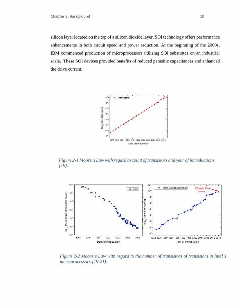
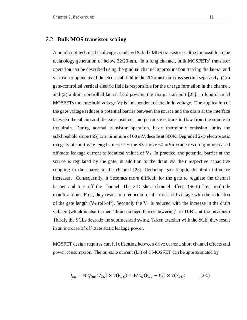
Figure 2-1 , whilst Figure 2-2 depict Moore’s Law with respect to the number of transistors
[19] and the processor area for Intel’s microprocessors, correspondingly [19]–[21].
A modern microprocessor contains a few billion transistors. Nowadays Moore’s Law is
slowed down by doubling the number of transistors on the chip every three years instead of
the original two years because the scaling of the transistors’ dimensions has become more
challenging [22]. Transistor scaling has a number of benefits over and above increasing the
on-chip transistor density [23]. For example, the delay of the logic gates is reduced and the
operating frequency of the transistors is increased by a factor of 1/Lg (where Lg = transistor
gate length) which permits faster circuit operation. For an equivalent degree of functionality,
the chip area is reduced by a factor of 1/(Lg)2 and this permits an increased number of dies
Chapter 2. Background 9
to be produced on a single wafer thereby reducing production costs. In addition, as the die
size is smaller, the quantity of defects per die is also reduced, resulting in an increased
manufacturing yield and productivity [24]. The active switching power per area stays steady,
with technology scaling permitting the circuits to operate at reduced power or permitting the
circuits to have greater functionality at fixed power. Whilst planar bulk silicon MOSFETs
have remained the backbone of the semiconductor industry in attaining constant scaling, the
bulk planar FET struggles to deliver scaling benefits beyond the 32/28nm CMOS technology
generation [25].
From the early 1990s the semiconductor industry and academia have worked together to
forecast the industry’s future. These efforts have been formalised in an international
organisation - the International Technology Roadmap for Semiconductors (ITRS) [26]
which remained in existence until 2015. The ITRS used to produce bi-annual reports which
contained predictions, recommendations and guidelines for the semiconductor industry. The
ITRS reports outlined the advancements of the technology, design tools, equipment and
metrology tools that need to be developed in order to maintain the exponential evolution of
the semiconductor chips needed to sustain Moore’s Law.
The backbone technology of the semiconductor industry is silicon Complementary Metal
Oxide Semiconductor (CMOS) technology, with the fundamental unit of CMOS chips being
the MOS Field Effect Transistor, the MOSFET. In order to keep up with the frenetic
development speed prescribed by Moore’s Law, transistor linear dimensions have decreased
by 70%, initially every two years, and since the beginning of this century every three years
the transistor and the chip areas have been reduced by 50% in every new technology
generation. The sub-micron dimension milestone was passed in the first half of the 1980s,
and this year (2018) regular mass production of the 7nm FinFET CMOS technology will be
in place with transistors with a 19nm gate length.
Although initially integrated circuits and the corresponding transistors were being
manufactured on “bulk” silicon wafers by the end of the 1990s, it was realised that major
performance enhancements could be achieved by introducing a novel type of substrate,
known as Silicon-On-Insulator (SOI) substrate. Here, transistors are produced in a thin
Chapter 2. Background 10
silicon layer located on the top of a silicon dioxide layer. SOI technology offers performance
enhancements in both circuit speed and power reduction. At the beginning of the 2000s,
IBM commenced production of microprocessors utilising SOI substrates on an industrial
scale. These SOI devices provided benefits of reduced parasitic capacitances and enhanced
the drive current.
Figure 2-1 Moore’s Law with regard to count of transistors and year of introductions
[19].
Figure 2-2 Moore’s Law with regard to the number of transistors of transistors in Intel’s
microprocessors [19-21].
Chapter 2. Background 11
Bulk MOS transistor scaling
A number of technical challenges rendered Si bulk MOS transistor scaling impossible in the
technology generation of below 22/20-nm. In a long channel, bulk MOSFETs’ transistor
operation can be described using the gradual channel approximation treating the lateral and
vertical components of the electrical field in the 2D transistor cross section separately: (1) a
gate-controlled vertical electric field is responsible for the charge formation in the channel,
and (2) a drain-controlled lateral field governs the charge transport [27]. In long channel
MOSFETs the threshold voltage VT is independent of the drain voltage. The application of
the gate voltage reduces a potential barrier between the source and the drain at the interface
between the silicon and the gate insulator and permits electrons to flow from the source to
the drain. During normal transistor operation, basic thermionic emission limits the
subthreshold slope (SS) to a minimum of 60 mV/decade at 300K. Degraded 2-D electrostatic
integrity at short gate lengths increases the SS above 60 mV/decade resulting in increased
off-state leakage current at identical values of VT. In practice, the potential barrier at the
source is regulated by the gate, in addition to the drain via their respective capacitive
coupling to the charge in the channel [28]. Reducing gate length, the drain influence
increases. Consequently, it becomes more difficult for the gate to regulate the channel
barrier and turn off the channel. The 2-D short channel effects (SCE) have multiple
manifestations. First, they result in a reduction of the threshold voltage with the reduction
of the gate length (VT roll-off). Secondly the VT is reduced with the increase in the drain
voltage (which is also termed ‘drain induced barrier lowering’, or DIBL, at the interface)
Thirdly the SCEs degrade the subthreshold swing. Taken together with the SCE, they result
in an increase of off-state static leakage power.
MOSFET design requires careful offsetting between drive current, short channel effects and
power consumption. The on-state current (Ion) of a MOSFET can be approximated by
𝐼𝑜𝑛 = 𝑊𝑄𝑖𝑛𝑣(𝑉𝐺𝐺) × 𝜈(𝑉𝐷𝐷) ≈ 𝑊𝐶𝐺(𝑉𝐺𝐺 − 𝑉𝑇) × 𝜈(𝑉𝐷𝐷) (2-1)
Chapter 2. Background 12
where W represents the device’s width, VT represents threshold voltage, Qinv represents the
inversion charge density at the maximum potential barrier near the source and 𝜈 represents
the velocity close to the source region (injection velocity) which is dependent on the drain
bias VDD. The power consumption (PC) can be estimated by
𝑃𝑑𝑖𝑠 = 𝐷𝑦𝑛𝑎𝑚𝑖𝑐 𝑝𝑜𝑤𝑒𝑟 + 𝑆𝑡𝑎𝑡𝑖𝑐 𝑝𝑜𝑤𝑒𝑟 (2-2)
𝐷𝑦𝑛𝑎𝑚𝑖𝑐 𝑝𝑜𝑤𝑒𝑟 = 𝛼𝑓𝐶𝑙𝑜𝑎𝑑𝑉𝐷𝐷 2 (2-3)
𝑆𝑡𝑎𝑡𝑖𝑐 𝑝𝑜𝑤𝑒𝑟 = 𝑉𝐷𝐷 (𝐼𝑙𝑒𝑎𝑘 + 𝐼𝑡ℎ10−(
𝑉𝑇𝑆𝑆⁄ ))
(2-4)
where α is the activity factor, f operating frequency, and SS is the sub-threshold slope, Ileak
represents the total leakage current from gate, the junctions and the band-to-band tunnelling,
and Ith is the drain current at VT. In order to maintain low power consumption, lower VDD
and leakage current, higher VT and a steeper SS is required according to equations (2-3 and
2-4). On the other hand, large gate capacitance, low VT and high injection velocity are
required to attain high performance in terms of saturation current.
To date, device engineers have tried to reduce SCE in short gate length devices using several
techniques. The first technique is by minimising the gate oxide thickness to enhance gate
control over the channel. The second technique is by reducing the source/drain junction
depth (particularly close to the gate edge, where the source/drain areas are known as
‘extensions’) in order to minimise the drain coupling the mobile charge in the channel and
its impact on the source barrier height. The third technique is by raising the degree of channel
doping to restrain the electric field lines which commence from the source and propagate
towards the drain and condoling the depletion and the inversion charge under the gate. In
contemporary bulk MOSFETs, bespoke channel doping is achieved by utilising complex
vertical and horizontal profiles in order to reduce the SCE. The creation of complex high
doping profiles in the channel incurs extra costs and also leads to a reduction in the transistor
performance (speed) together with an increased static leakage current due to enhanced band-
Chapter 2. Background 13
to-band tunnelling and gate induced drain leakage (GIDL). When the gate oxide becomes
2nm thick, quantum mechanical tunnelling leads to an increase in the gate leakage current.
For oxides thinner than 2nm, the direct-tunnelling gate leakage current sharply increases
(~3X for each 1 Ao reduction in oxide thickness). This gate leakage increases the standby
power consumption and in addition can interfere with proper logic gate operation. As a
consequence, most foundries now have replaced the conventional silicon dioxide (SiO2) as
a gate dielectric with high permittivity (high-k) gate dielectrics [29], predominantly hafnia
(HfO2). This results in high gate capacitance with physically thick insulators with very low
probability of tunnelling. Nevertheless, the introduction of such new materials is not without
challenges and achieving the desired results with no associated losses in mobility and
reliability is currently a field of intensive further research.
Another challenge is the resistance of the source/drain regions. For example, when the
source/drain junction depths are reduced to control SCE, there is a need to increase doping
levels in order to maintain constant sheet resistance. The upper limit for the solid solubility
of dopants is around 1020 cm−3 depending on the dopant space. Consequently, the reductions
in junction depth lead to raised series resistance reducing the performance of the transistor.
Simultaneously, from a technological perspective, the formation of ultra-shallow junctions
which does not diffuse deeper following doping activation annealing, required to achieve
low resistivity [28], [30] becomes difficult. With increasing doping density in the channel
for SCE suppression, the carrier mobility is degraded as a consequence of increased ionized
impurity scattering. Furthermore, the subthreshold slope deteriorates as a consequence of
increased depletion capacitance which impedes the control of the surface potential by the
gate voltage. Due to very high channel doping close to the source/drain extensions, an
additional static leakage mechanism, band-to-band tunnelling (BTBT), becomes significant.
Lastly, with reducing channel volume in extremely scaled transistors, the stochastic
positioning of discrete dopant atoms leads to random inter-device variations.
The requirement to increase drive currents with transistor scaling and to reduce the supply
voltage is associated with an exponential increase in the static, off-state leakage of the
transistor. Although the active power density of the chip has grown steadily with the gate
length scaling, the static power density has increased much more rapidly. The active power
Chapter 2. Background 14
is a consequence of the dissipative current flow through the complementary CMOS
transistor pairs during logic switching. The sub-threshold, static or standby power is
dissipated even when the integrated circuit is inactive. The subthreshold leakage was the
major leakage mechanisms for long channel transistors. For contemporary nano-scaled bulk
MOSFETs BTBT, GIDL and gate leakage dominate the static power dissipation. Whilst
static power dissipation was a relatively minor issue a few decades ago, in the latest 28nm
and 20nm bulk technology generations it compares in magnitude to the active power.
Control and suppression of static power became a major issue for continued gate length
scaling in bulk CMOS technology marking eventually its end. The needed higher channel
doping and halo implant required to regulate SCE also increases the source/drain to bulk
parasitic capacitances slowing the speed in the latest generations’ bulk MOSFETs.
Due to the deficiencies in performance, insufficient control of the CER and exploding power
consumption, traditional bulk MOSFETs reached the end of their scaling and useful life with
the 20nm bulk CMOS technology which has been introduced into production by only one
foundry: TSMC. New device architectures aiming to replace the conventional bulk CMOS
in combination with a new channel and gate stack materials have been driving
semiconductor research over the past two decades [31], [32].
Figure 2-3 Typical PDSOI (a) and(b) FDSOI structures [32].
Chapter 2. Background 15
SOI MOSFETs
The first alternative to the bulk MOSFET adopted commercially is the SOI transistor. As
depicted in Figure 2-3, two types of SOI transistors exist: partially depleted (PD) and fully
depleted (FD). In the PD SOI MOSFETs, a stratum of insulating SiO2 divides the top device-
containing layer from the bulk Si underneath. The PD MOSFET has a similar design and
similar dimensions to a bulk MOSFET [28]. When in the OFF state, the depletion depth
beneath the gate is below the depth of the top silicon layer [33]. The PD MOSFET delivers
reduced parasitic Source/Drain capacitance in an inverter circuit, reducing the propagation
delay and increasing switching speeds. The potential of the floating body is controlled
dynamically by capacitive coupling of the range of electrodes associated with this layer.
Therefore, a floating charge can build up in this area, leading to modification of the floating-
body charge and the historical effects of transistor characteristics [34]–[39] . Such floating
body voltage can alter the threshold voltage of the device, potentially resulting in serious
discrepancies between two identical transistors [40]–[42].
PD MOSFET techniques have been successfully applied to high volume production,
although this encounters the same challenges associated with scaling as the bulk MOSFET
and therefore this is not a scalable technology with a long-term future [43].
A further issue with SOI transistors is self-heating [44], [45]. In SOI circuits, the active
transistors are positioned on top of a thermally insulating layer of silicon oxide. When the
circuit is in operation, the power generated in the active region cannot be easily dissipated
through the silicon substrate. Consequently, the temperature of the silicon body increases
resulting in a reduction in mobility and in drive current.
In the fully Depleted (FDSOI) MOSFET the top silicon film is thinned down to such an
extent that it becomes entirely depleted in the OFF state (see Figure 2-3). Elimination of the
partially depleted region in the FDSOI MOSFET enables suppression of the floating body
effects. The reduction of the silicon film thickness also allows better control of the short
channel effects and therefore tolerates a reduction in the channel doping densities. In
addition, the vertical electric field is reduced for the same channel carrier concentration.
Chapter 2. Background 16
Therefore, the inversion layer mobility is enhanced without detrimentally affecting the OFF-
state current. Hence, by increasing the buried oxide thickness, optimal subthreshold slopes
of 60 mV/decade can be attained. However, this also increases the drain control on the
source-channel barrier via the buried oxide. Employment of a thin buried oxide can
overcome this problem through the termination of the drain field lines on the back substrate,
but at the cost of a degraded sub-threshold slope [34], [46]–[50].
Multi-Gate MOSFETs
The channel gate control is improved by the structural positioning of the gate close to the
channel. Improved gate control may also be achieved by utilising more gates. Multi-gate
MOSFETs can be considered an extension of the fully-depleted SOI MOSFETs, but with a
greater number of gates around the thin silicon body. Multi-gate MOSFETs provide greater
electrostatic control of the inversion channel [51].
The improved electrostatic control in the multi-gate MOSFET minimises the detrimental
short channel effects (SCE) and improves the scalability of multi-gate FETs compared to
planar bulk MOSFETs. To achieve this, planar double-gate [52], fully Depleted Lean-
channel Transistor (DELTA) [53], vertical double-gate (FinFET) [54]–[56], omega-shaped
gate (Ω-gate) [57], [58], Φ-FET[59], and Gate-All-Around (GAA) nanowire [59]–[63] have
been proposed by researchers over the last fifteen years.
The double-gate MOSFET has a symmetrical device structure where the channel is
controlled by a gate on either side of the Si layer. Better gate control allows further reduction
of the Si film thickness for a similar gate length compared with FD-SOI at an identical OFF-
state current. Appropriate device design enables volume inversion in the thin Si film, where
the majority of the inversion charge resides at the Si film centre, and the vertical field results
in greatly enhanced mobility. Due to better electrostatic integrity delivered by the two gates,
the channel length can be reduced further, compared with FDSOI.
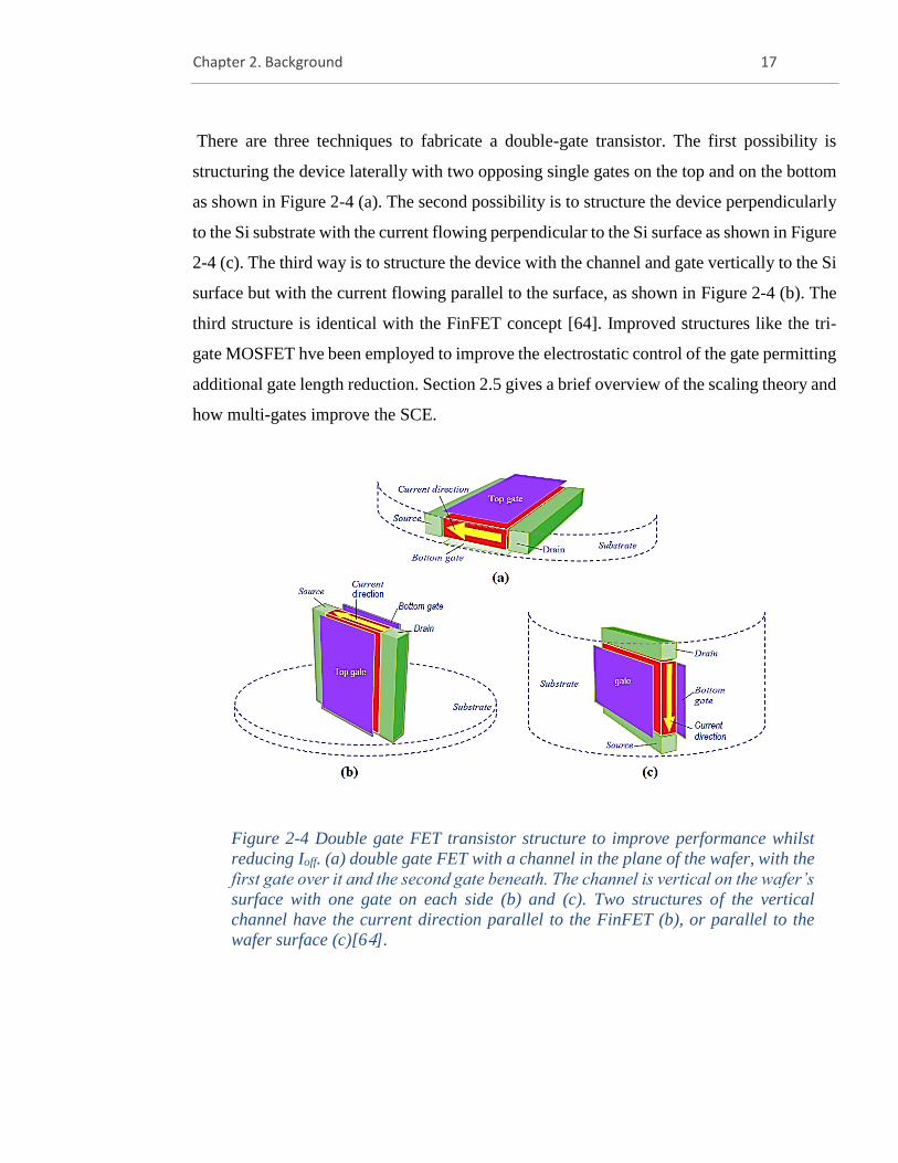
Chapter 2. Background 17
There are three techniques to fabricate a double-gate transistor. The first possibility is
structuring the device laterally with two opposing single gates on the top and on the bottom
as shown in Figure 2-4 (a). The second possibility is to structure the device perpendicularly
to the Si substrate with the current flowing perpendicular to the Si surface as shown in Figure
2-4 (c). The third way is to structure the device with the channel and gate vertically to the Si
surface but with the current flowing parallel to the surface, as shown in Figure 2-4 (b). The
third structure is identical with the FinFET concept [64]. Improved structures like the tri-
gate MOSFET hve been employed to improve the electrostatic control of the gate permitting
additional gate length reduction. Section 2.5 gives a brief overview of the scaling theory and
how multi-gates improve the SCE.
Figure 2-4 Double gate FET transistor structure to improve performance whilst
reducing Ioff. (a) double gate FET with a channel in the plane of the wafer, with the
first gate over it and the second gate beneath. The channel is vertical on the wafer’s
surface with one gate on each side (b) and (c). Two structures of the vertical
channel have the current direction parallel to the FinFET (b), or parallel to the
wafer surface (c)[64].
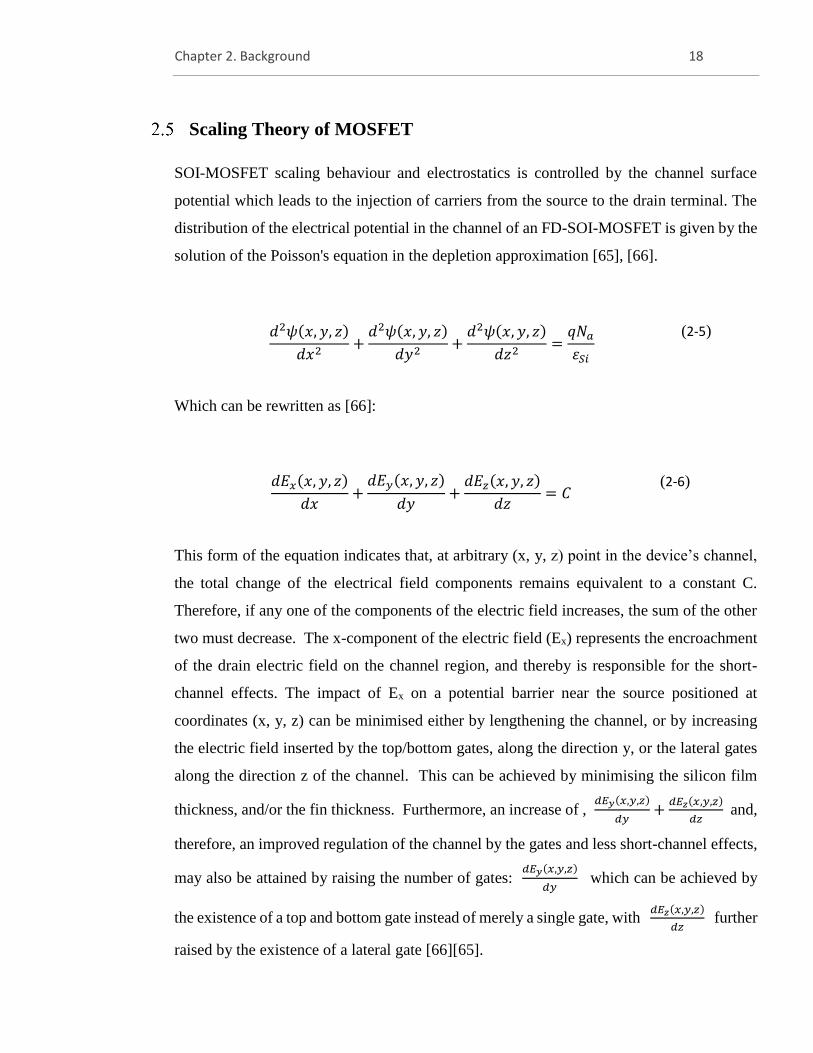
Chapter 2. Background 18
Scaling Theory of MOSFET
SOI-MOSFET scaling behaviour and electrostatics is controlled by the channel surface
potential which leads to the injection of carriers from the source to the drain terminal. The
distribution of the electrical potential in the channel of an FD-SOI-MOSFET is given by the
solution of the Poisson's equation in the depletion approximation [65], [66].
𝑑2𝜓(𝑥, 𝑦, 𝑧)
𝑑𝑥2+
𝑑2𝜓(𝑥, 𝑦, 𝑧)
𝑑𝑦2+
𝑑2𝜓(𝑥, 𝑦, 𝑧)
𝑑𝑧2=
𝑞𝑁𝑎
휀𝑆𝑖
(2-5)
Which can be rewritten as [66]:
𝑑𝐸𝑥(𝑥, 𝑦, 𝑧)
𝑑𝑥+
𝑑𝐸𝑦(𝑥, 𝑦, 𝑧)
𝑑𝑦+
𝑑𝐸𝑧(𝑥, 𝑦, 𝑧)
𝑑𝑧= 𝐶
(2-6)
This form of the equation indicates that, at arbitrary (x, y, z) point in the device’s channel,
the total change of the electrical field components remains equivalent to a constant C.
Therefore, if any one of the components of the electric field increases, the sum of the other
two must decrease. The x-component of the electric field (Ex) represents the encroachment
of the drain electric field on the channel region, and thereby is responsible for the short-
channel effects. The impact of Ex on a potential barrier near the source positioned at
coordinates (x, y, z) can be minimised either by lengthening the channel, or by increasing
the electric field inserted by the top/bottom gates, along the direction y, or the lateral gates
along the direction z of the channel. This can be achieved by minimising the silicon film
thickness, and/or the fin thickness. Furthermore, an increase of , 𝑑𝐸𝑦(𝑥,𝑦,𝑧)
𝑑𝑦+
𝑑𝐸𝑧(𝑥,𝑦,𝑧)
𝑑𝑧 and,
therefore, an improved regulation of the channel by the gates and less short-channel effects,
may also be attained by raising the number of gates: 𝑑𝐸𝑦(𝑥,𝑦,𝑧)
𝑑𝑦 which can be achieved by
the existence of a top and bottom gate instead of merely a single gate, with 𝑑𝐸𝑧(𝑥,𝑦,𝑧)
𝑑𝑧 further
raised by the existence of a lateral gate [66][65].
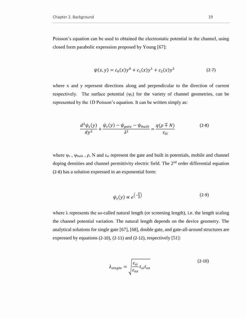
Chapter 2. Background 19
Poisson’s equation can be used to obtained the electrostatic potential in the channel, using
closed form parabolic expression proposed by Young [67]:
𝜓(𝑥, 𝑦) = 𝑐0(𝑥)𝑦0 + 𝑐1(𝑥)𝑦1 + 𝑐2(𝑥)𝑦2 (2-7)
where x and y represent directions along and perpendicular to the direction of current
respectively. The surface potential (ψs) for the variety of channel geometries, can be
represented by the 1D Poisson’s equation. It can be written simply as:
𝑑2𝜓𝑠(𝑦)
𝑑𝑦2+
𝜓𝑠(𝑦) − 𝜓𝑔𝑎𝑡𝑒 − 𝜓𝑏𝑢𝑖𝑙𝑡
𝜆2=
𝑞(𝜌 ∓ 𝑁)
휀𝑆𝑖
(2-8)
where ψs , ψbuilt , ρ, N and εsi represent the gate and built in potentials, mobile and channel
doping densities and channel permittivity electric field. The 2nd order differential equation
(2-8) has a solution expressed in an exponential form:
𝜓𝑠(𝑦) ∝ 𝑒(−𝑦𝜆
)
(2-9)
where λ represents the so-called natural length (or screening length), i.e. the length scaling
the channel potential variation. The natural length depends on the device geometry. The
analytical solutions for single gate [67], [68], double gate, and gate-all-around structures are
expressed by equations (2-10), (2-11) and (2-12), respectively [51]:
𝜆𝑠𝑖𝑛𝑔𝑙𝑒 = √휀𝑠𝑖
휀𝑜𝑥𝑡𝑠𝑖𝑡𝑜𝑥
(2-10)
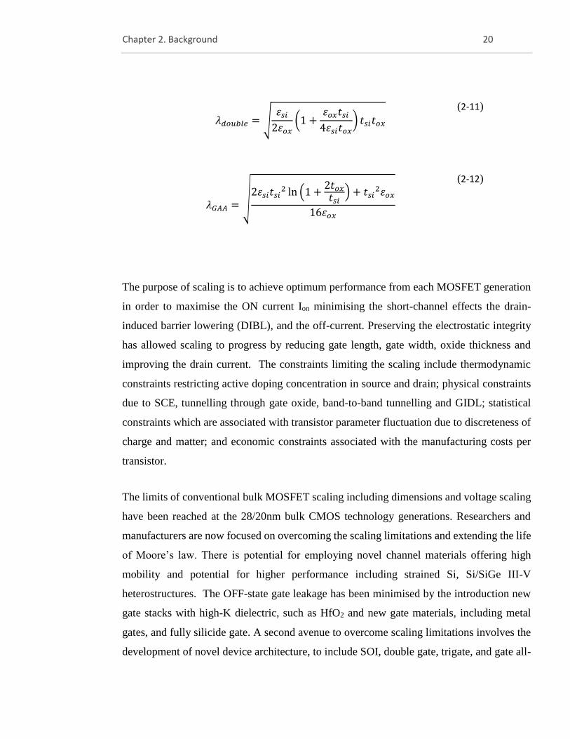
Chapter 2. Background 20
𝜆𝑑𝑜𝑢𝑏𝑙𝑒 = √휀𝑠𝑖
2휀𝑜𝑥(1 +
휀𝑜𝑥𝑡𝑠𝑖
4휀𝑠𝑖𝑡𝑜𝑥) 𝑡𝑠𝑖𝑡𝑜𝑥
(2-11)
𝜆𝐺𝐴𝐴 =√
2휀𝑠𝑖𝑡𝑠𝑖2 ln (1 +
2𝑡𝑜𝑥
𝑡𝑠𝑖) + 𝑡𝑠𝑖
2휀𝑜𝑥
16휀𝑜𝑥
(2-12)
The purpose of scaling is to achieve optimum performance from each MOSFET generation
in order to maximise the ON current Ion minimising the short-channel effects the drain-
induced barrier lowering (DIBL), and the off-current. Preserving the electrostatic integrity
has allowed scaling to progress by reducing gate length, gate width, oxide thickness and
improving the drain current. The constraints limiting the scaling include thermodynamic
constraints restricting active doping concentration in source and drain; physical constraints
due to SCE, tunnelling through gate oxide, band-to-band tunnelling and GIDL; statistical
constraints which are associated with transistor parameter fluctuation due to discreteness of
charge and matter; and economic constraints associated with the manufacturing costs per
transistor.
The limits of conventional bulk MOSFET scaling including dimensions and voltage scaling
have been reached at the 28/20nm bulk CMOS technology generations. Researchers and
manufacturers are now focused on overcoming the scaling limitations and extending the life
of Moore’s law. There is potential for employing novel channel materials offering high
mobility and potential for higher performance including strained Si, Si/SiGe III-V
heterostructures. The OFF-state gate leakage has been minimised by the introduction new
gate stacks with high-K dielectric, such as HfO2 and new gate materials, including metal
gates, and fully silicide gate. A second avenue to overcome scaling limitations involves the
development of novel device architecture, to include SOI, double gate, trigate, and gate all-
Chapter 2. Background 21
around GAA transistors enhancing the electrostatic integrity and also relaxing the limit of
the oxide scaling.
FinFETs
The fully depleted double gate SOI structure (or delta FET) was initially experimentally
suggested by Hisamato et. al. in 1989 [69]. Chenming Hu and his team reported the idea of
FinFET in 1999 and UTB-SOI (FD SOI) in 2000 [70]. The fundamental concept underlying
both innovations is a very thin body (approximately 10nm or less), enabling the gate to be
coupled strongly to the channel with no leakage path a great distance from the gate. As a
result, the gate is able to control the leakage current much better. FinFETs possess include
the formation of a vertical channel known as the Fin, so the channel width of a FinFET is
defined in terms of fin height resulting in channel ‘width quantization’ (single, double or
multiple fins). Therefore, the current in the FinFETs can be increased by increasing the fin
numbers retaining the improved gate control over the channel charge. fin height determines
the structural stability of the FinFET: the smaller the Fin height the more stable the structure
is.
FinFETs can be fabricated on bulk silicon wafers where all fins share a common silicon
substrate. In this case shallow trench insolation and punch-through doping are used to isolate
the individual fins. In the case of SOI FinFETs the fins are naturally isolated by the buried
oxide layer. Figure 2-5 schematically compares bulk and SOI FinFETs.
The first generation of multi-gate transistors with three-sided gate control has been
manufactured by Intel at their 22nm node with 90nm fin pitch and 34nm fin height featuring
a 3rd-generation high-k metal-gate technology and a 5th generation of channel strain
techniques. The lower threshold voltage combined with the strain enhancement have lead to
a 13% and 27% increase in Idsat in N and P channel FinFETs respectively at 0.8V and
10nA/um leakage current compared with the 28nm CMOS technology [71], [72].
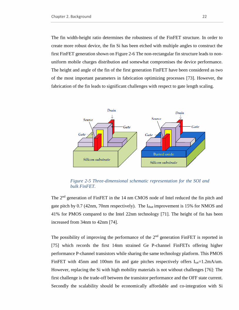
Chapter 2. Background 22
The fin width-height ratio determines the robustness of the FinFET structure. In order to
create more robust device, the fin Si has been etched with multiple angles to construct the
first FinFET generation shown on Figure 2-6 The non-rectangular fin structure leads to non-
uniform mobile charges distribution and somewhat compromises the device performance.
The height and angle of the fin of the first generation FinFET have been considered as two
of the most important parameters in fabrication optimizing processes [73]. However, the
fabrication of the fin leads to significant challenges with respect to gate length scaling.
The 2nd generation of FinFET in the 14 nm CMOS node of Intel reduced the fin pitch and
gate pitch by 0.7 (42nm, 70nm respectively). The Idsat improvement is 15% for NMOS and
41% for PMOS compared to the Intel 22nm technology [71]. The height of fin has been
increased from 34nm to 42nm [74].
The possibility of improving the performance of the 2nd generation FinFET is reported in
[75] which records the first 14nm strained Ge P-channel FinFETs offering higher
performance P-channel transistors while sharing the same technology platform. This PMOS
FinFET with 45nm and 100nm fin and gate pitches respectively offers Isat=1.2mA/um.
However, replacing the Si with high mobility materials is not without challenges [76]: The
first challenge is the trade-off between the transistor performance and the OFF state current.
Secondly the scalability should be economically affordable and co-integration with Si
Figure 2-5 Three-dimensional schematic representation for the SOI and
bulk FinFET.
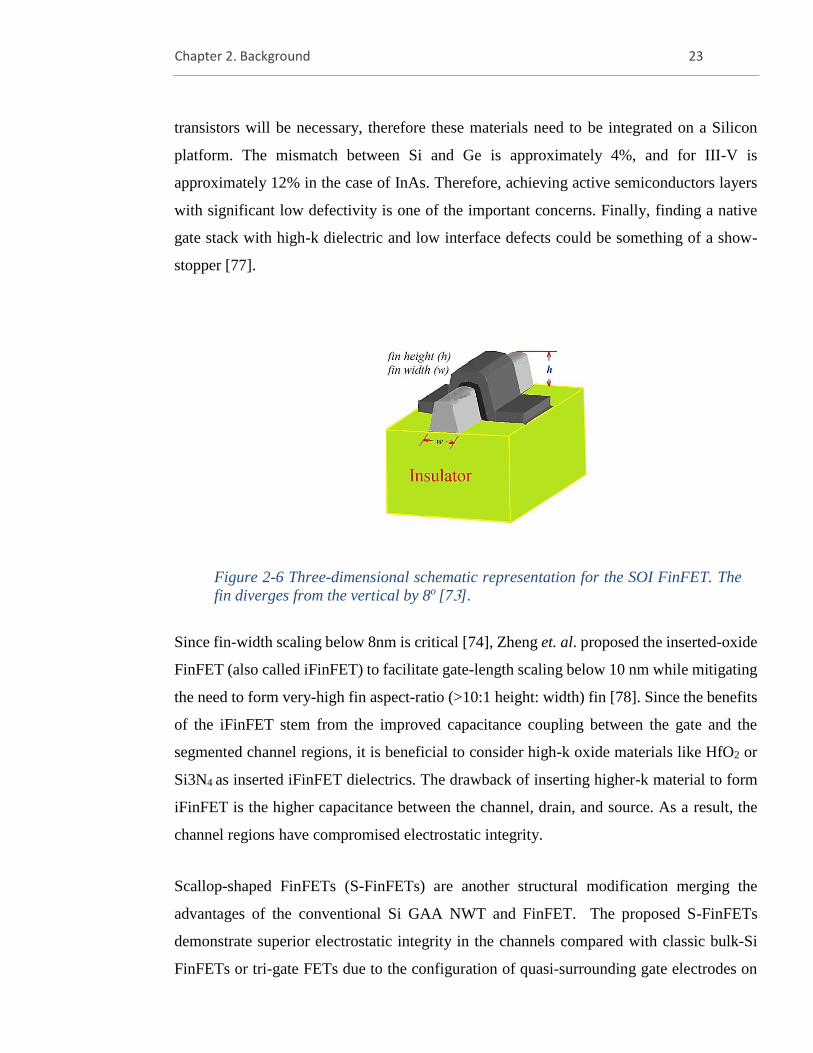
Chapter 2. Background 23
transistors will be necessary, therefore these materials need to be integrated on a Silicon
platform. The mismatch between Si and Ge is approximately 4%, and for III-V is
approximately 12% in the case of InAs. Therefore, achieving active semiconductors layers
with significant low defectivity is one of the important concerns. Finally, finding a native
gate stack with high-k dielectric and low interface defects could be something of a show-
stopper [77].
Since fin-width scaling below 8nm is critical [74], Zheng et. al. proposed the inserted-oxide
FinFET (also called iFinFET) to facilitate gate-length scaling below 10 nm while mitigating
the need to form very-high fin aspect-ratio (>10:1 height: width) fin [78]. Since the benefits
of the iFinFET stem from the improved capacitance coupling between the gate and the
segmented channel regions, it is beneficial to consider high-k oxide materials like HfO2 or
Si3N4 as inserted iFinFET dielectrics. The drawback of inserting higher-k material to form
iFinFET is the higher capacitance between the channel, drain, and source. As a result, the
channel regions have compromised electrostatic integrity.
Scallop-shaped FinFETs (S-FinFETs) are another structural modification merging the
advantages of the conventional Si GAA NWT and FinFET. The proposed S-FinFETs
demonstrate superior electrostatic integrity in the channels compared with classic bulk-Si
FinFETs or tri-gate FETs due to the configuration of quasi-surrounding gate electrodes on
Figure 2-6 Three-dimensional schematic representation for the SOI FinFET. The
fin diverges from the vertical by 8o [73].
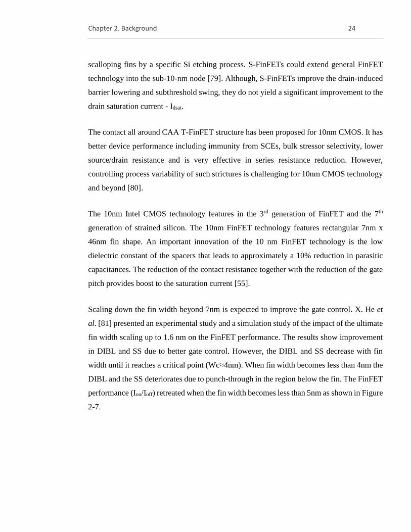
Chapter 2. Background 24
scalloping fins by a specific Si etching process. S-FinFETs could extend general FinFET
technology into the sub-10-nm node [79]. Although, S-FinFETs improve the drain-induced
barrier lowering and subthreshold swing, they do not yield a significant improvement to the
drain saturation current - Idsat.
The contact all around CAA T-FinFET structure has been proposed for 10nm CMOS. It has
better device performance including immunity from SCEs, bulk stressor selectivity, lower
source/drain resistance and is very effective in series resistance reduction. However,
controlling process variability of such strictures is challenging for 10nm CMOS technology
and beyond [80].
The 10nm Intel CMOS technology features in the 3rd generation of FinFET and the 7th
generation of strained silicon. The 10nm FinFET technology features rectangular 7nm x
46nm fin shape. An important innovation of the 10 nm FinFET technology is the low
dielectric constant of the spacers that leads to approximately a 10% reduction in parasitic
capacitances. The reduction of the contact resistance together with the reduction of the gate
pitch provides boost to the saturation current [55].
Scaling down the fin width beyond 7nm is expected to improve the gate control. X. He et
al. [81] presented an experimental study and a simulation study of the impact of the ultimate
fin width scaling up to 1.6 nm on the FinFET performance. The results show improvement
in DIBL and SS due to better gate control. However, the DIBL and SS decrease with fin
width until it reaches a critical point (Wc≈4nm). When fin width becomes less than 4nm the
DIBL and the SS deteriorates due to punch-through in the region below the fin. The FinFET
performance (Ion/Ioff) retreated when the fin width becomes less than 5nm as shown in Figure
2-7.
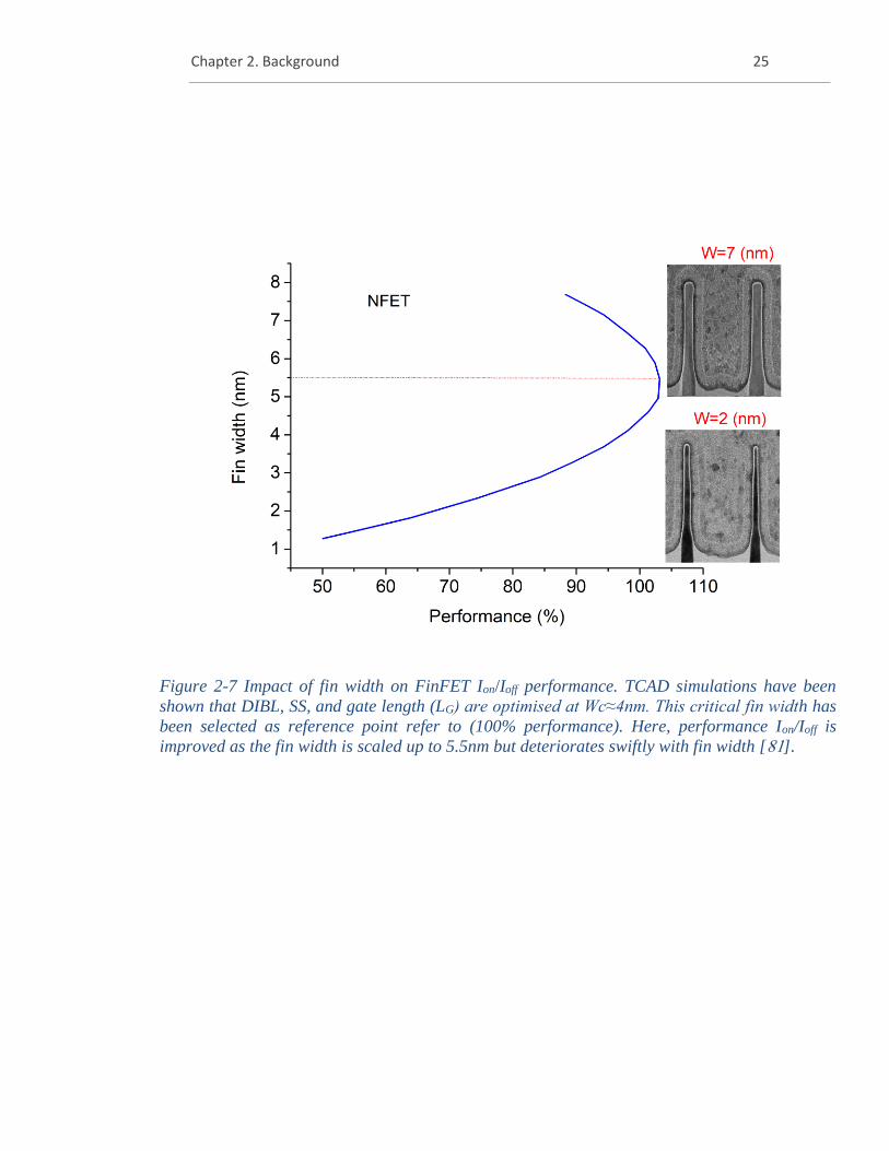
Chapter 2. Background 25
Figure 2-7 Impact of fin width on FinFET Ion/Ioff performance. TCAD simulations have been
shown that DIBL, SS, and gate length (LG) are optimised at Wc≈4nm. This critical fin width has
been selected as reference point refer to (100% performance). Here, performance Ion/Ioff is
improved as the fin width is scaled up to 5.5nm but deteriorates swiftly with fin width [81].
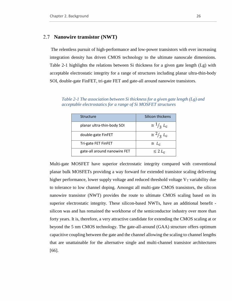
Chapter 2. Background 26
Nanowire transistor (NWT)
The relentless pursuit of high-performance and low-power transistors with ever increasing
integration density has driven CMOS technology to the ultimate nanoscale dimensions.
Table 2-1 highlights the relations between Si thickness for a given gate length (Lg) with
acceptable electrostatic integrity for a range of structures including planar ultra-thin-body
SOI, double-gate FinFET, tri-gate FET and gate-all around nanowire transistors.
Multi-gate MOSFET have superior electrostatic integrity compared with conventional
planar bulk MOSFETs providing a way forward for extended transistor scaling delivering
higher performance, lower supply voltage and reduced threshold voltage VT variability due
to tolerance to low channel doping. Amongst all multi-gate CMOS transistors, the silicon
nanowire transistor (NWT) provides the route to ultimate CMOS scaling based on its
superior electrostatic integrity. These silicon-based NWTs, have an additional benefit -
silicon was and has remained the workhorse of the semiconductor industry over more than
forty years. It is, therefore, a very attractive candidate for extending the CMOS scaling at or
beyond the 5 nm CMOS technology. The gate-all-around (GAA) structure offers optimum
capacitive coupling between the gate and the channel allowing the scaling to channel lengths
that are unattainable for the alternative single and multi-channel transistor architectures
[66].
Table 2-1 The association between Si thickness for a given gate length (Lg) and
acceptable electrostatics for a range of Si MOSFET structures
Structure Silicon thickens
planar ultra-thin-body SOI ≅ 13 ⁄ 𝐿𝐺
double-gate FinFET ≅ 23 ⁄ 𝐿𝐺
Tri-gate FET FinFET ≅ 𝐿𝐺
gate-all around nanowire FET ≤ 2 𝐿𝐺
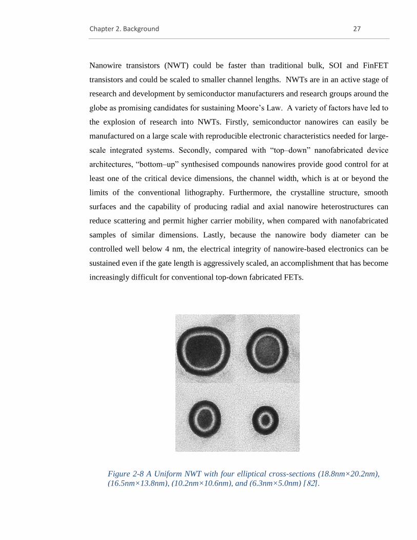
Chapter 2. Background 27
Nanowire transistors (NWT) could be faster than traditional bulk, SOI and FinFET
transistors and could be scaled to smaller channel lengths. NWTs are in an active stage of
research and development by semiconductor manufacturers and research groups around the
globe as promising candidates for sustaining Moore’s Law. A variety of factors have led to
the explosion of research into NWTs. Firstly, semiconductor nanowires can easily be
manufactured on a large scale with reproducible electronic characteristics needed for large-
scale integrated systems. Secondly, compared with “top–down” nanofabricated device
architectures, “bottom–up” synthesised compounds nanowires provide good control for at
least one of the critical device dimensions, the channel width, which is at or beyond the
limits of the conventional lithography. Furthermore, the crystalline structure, smooth
surfaces and the capability of producing radial and axial nanowire heterostructures can
reduce scattering and permit higher carrier mobility, when compared with nanofabricated
samples of similar dimensions. Lastly, because the nanowire body diameter can be
controlled well below 4 nm, the electrical integrity of nanowire-based electronics can be
sustained even if the gate length is aggressively scaled, an accomplishment that has become
increasingly difficult for conventional top-down fabricated FETs.
Figure 2-8 A Uniform NWT with four elliptical cross-sections (18.8nm×20.2nm),
(16.5nm×13.8nm), (10.2nm×10.6nm), and (6.3nm×5.0nm) [82].
Chapter 2. Background 28
Bangsaruntip et al have developed a fabrication process to fabricate a highly uniform NWT
with an elliptical cross-section (see Figure 2-8). Several NWTs with different cross-sectional
areas (190π-15.75π) have been made in order to find the impact of NWT diameter on SCE
[82]. Characterisation results have shown that a good electrostatic control and satisfactory
drive currents, for example the drive current of an elliptical NWT with the cross-section
(9nmx13.6nm) is 0.95 mA/µm. There is a significant dependency of the SCE against wire
size [82].
Over the past three years many scenarios have been proposed to scale NWTs. R. Kim et
al., present an NWT performance guideline based on atomistic quantum transport simulation
including strain effects for Ge, Si, GaAs, and InAs NWT with a 13nm gate length. Results
have shown that a Ge NWT with improved source and drain design could deliver better
current versus delay performance whilst III-V NWTs have shown themselves to be superior
for power reduction capacitance [83]. Y. Lee et al., presented an experimental way to scale
the Ge and Ge0.9Si0.1 NWT with an unusual diamond-shape [84]. An experimental study
endorses simulations on industry-related solutions for FinFET and NWT based on different
semiconductors such as Si, Ge, and III-V. A substantial impact on self-heating effects was
observed by converting from FinFET to NWT. However, modifying the S/D doping or the
material of the gate had a little impact on self-heating effects [85]. Another comprehensive
study based on state-of-the-art physical models has examined the performance, reliability
limits, and variability of 10 nm technology and beyond based on NWT. there have been
indication of degradation of ON current of NWT technology compared to FinFETs [86].
Bangsaruntip et al (IBM) have demonstrated for the first time that Si NWT can be integrated
to density targets equivalent to CMOS scaling target of the 10 nm technology. This scaled
NWT achieves a good performance (The Ion at VDD = 1.0 V 0.976 mA/μm) [87]. The
perpendicular stacked NWT architecture, designed for sub-7nm CMOS technology, can
offer considerable benefits such as low off-state current thanks to gate all around
electrostatic control, whilst this structure drive high on-state current thanks to 3-D vertically
stacked channels [88]. The stacked NWT structure has been utilised to construct a
functioning ring oscillator [89]. Nanosheet devices are a special case of NWT considered at
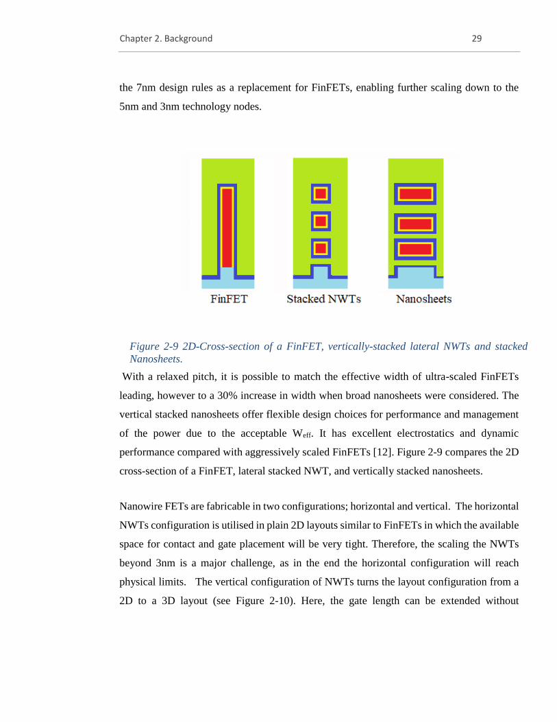
Chapter 2. Background 29
the 7nm design rules as a replacement for FinFETs, enabling further scaling down to the
5nm and 3nm technology nodes.
With a relaxed pitch, it is possible to match the effective width of ultra-scaled FinFETs
leading, however to a 30% increase in width when broad nanosheets were considered. The
vertical stacked nanosheets offer flexible design choices for performance and management
of the power due to the acceptable Weff. It has excellent electrostatics and dynamic
performance compared with aggressively scaled FinFETs [12]. Figure 2-9 compares the 2D
cross-section of a FinFET, lateral stacked NWT, and vertically stacked nanosheets.
Nanowire FETs are fabricable in two configurations; horizontal and vertical. The horizontal
NWTs configuration is utilised in plain 2D layouts similar to FinFETs in which the available
space for contact and gate placement will be very tight. Therefore, the scaling the NWTs
beyond 3nm is a major challenge, as in the end the horizontal configuration will reach
physical limits. The vertical configuration of NWTs turns the layout configuration from a
2D to a 3D layout (see Figure 2-10). Here, the gate length can be extended without
Figure 2-9 2D-Cross-section of a FinFET, vertically-stacked lateral NWTs and stacked
Nanosheets.
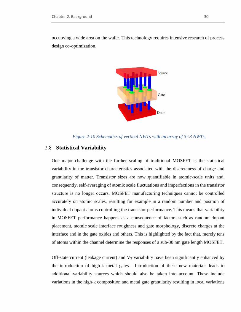
Chapter 2. Background 30
occupying a wide area on the wafer. This technology requires intensive research of process
design co-optimization.
Statistical Variability
One major challenge with the further scaling of traditional MOSFET is the statistical
variability in the transistor characteristics associated with the discreteness of charge and
granularity of matter. Transistor sizes are now quantifiable in atomic-scale units and,
consequently, self-averaging of atomic scale fluctuations and imperfections in the transistor
structure is no longer occurs. MOSFET manufacturing techniques cannot be controlled
accurately on atomic scales, resulting for example in a random number and position of
individual dopant atoms controlling the transistor performance. This means that variability
in MOSFET performance happens as a consequence of factors such as random dopant
placement, atomic scale interface roughness and gate morphology, discrete charges at the
interface and in the gate oxides and others. This is highlighted by the fact that, merely tens
of atoms within the channel determine the responses of a sub-30 nm gate length MOSFET.
Off-state current (leakage current) and VT variability have been significantly enhanced by
the introduction of high-k metal gates. Introduction of these new materials leads to
additional variability sources which should also be taken into account. These include
variations in the high-k composition and metal gate granularity resulting in local variations
Figure 2-10 Schematics of vertical NWTs with an array of 3×3 NWTs.
Chapter 2. Background 31
of the gate work function. Intrinsic parameter fluctuations already represent a significant
challenge for the semiconductor industry and the forecast is that they will continue to be an
important issue in the future.
Both systematic and statistical sources of variation are present at the device level. Systematic
variation represents a sub-class of process variability, which is layout dependent, and is a
result of strain and lithography including proximity effects, (e.g. imperfections in
lithography processes) which are predominantly deterministic and predictable, however
complex. Consequently, they are controllable to a certain extent with compensation
techniques available at the circuit design stage. As an example, distortions which take place
during the photo-lithography process can be corrected by employment of the Optical
Proximity Correction (OPC). Furthermore, strain, which is commonly employed to improve
transistor performance, leads to both microscopic statistical variations and larger scale
deterministic variations which are predominantly are due to the effects of the circuitry
layout. In this instance, the layout dependent variations could be more significant than the
local fluctuations and consequently, strain can be effectively regarded as a systematic
variability source and its impact could be examined using TCAD tools. A more serious
challenge, however, are entirely statistical intrinsic parameter fluctuations and their inherent
stochasticity. Statistical fluctuations are caused by the fundamental discreteness of charge
and granularity of matter which are impossible to accurately control (e.g. the arrangement
of dopant atoms in a device). These variability sources are responsible for in excess of 50%
of the total variability in the 45/40 nm technology generation and have a much more
pronounced effect at the 32nm technology. It is therefore clear that statistical fluctuations
are of key significance to CMOS scaling and integration in the future.
Random discrete dopants (RDDs) in the channel and source/drain regions are the
predominant source of statistical variability in modern bulk MOSFETs, in the 45/40 nm and
32/28 nm technology generations. Whilst RDDs are the predominant source of statistical
variability, the contribution of line edge roughness (LER) increases in significance because
LER scaling currently lags behind ITRS requirements. Whilst innovative device
architectures such as SOI and multi-gate MOS FETs tolerate low channel doping, resulting
in reduced RDD variability, they are liable to LER effects. Line edge roughness is a
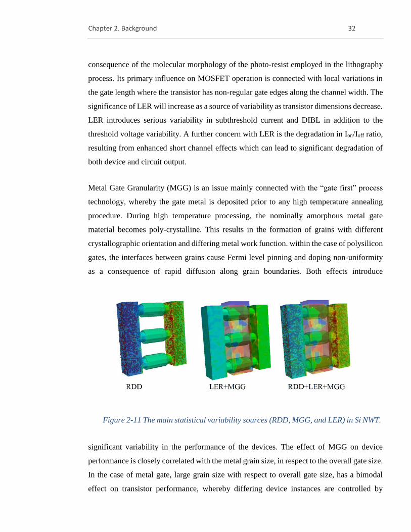
Chapter 2. Background 32
consequence of the molecular morphology of the photo-resist employed in the lithography
process. Its primary influence on MOSFET operation is connected with local variations in
the gate length where the transistor has non-regular gate edges along the channel width. The
significance of LER will increase as a source of variability as transistor dimensions decrease.
LER introduces serious variability in subthreshold current and DIBL in addition to the
threshold voltage variability. A further concern with LER is the degradation in Ion/Ioff ratio,
resulting from enhanced short channel effects which can lead to significant degradation of
both device and circuit output.
Metal Gate Granularity (MGG) is an issue mainly connected with the “gate first” process
technology, whereby the gate metal is deposited prior to any high temperature annealing
procedure. During high temperature processing, the nominally amorphous metal gate
material becomes poly-crystalline. This results in the formation of grains with different
crystallographic orientation and differing metal work function. within the case of polysilicon
gates, the interfaces between grains cause Fermi level pinning and doping non-uniformity
as a consequence of rapid diffusion along grain boundaries. Both effects introduce
significant variability in the performance of the devices. The effect of MGG on device
performance is closely correlated with the metal grain size, in respect to the overall gate size.
In the case of metal gate, large grain size with respect to overall gate size, has a bimodal
effect on transistor performance, whereby differing device instances are controlled by
Figure 2-11 The main statistical variability sources (RDD, MGG, and LER) in Si NWT.
Chapter 2. Background 33
different grain work functions. Interestingly, small grain size, relative to overall gate area,
causes self-averaging of the grain work functions and has a smaller influence on overall
device performance. In the gate last processes, where the gate is deposited post annealing
(and other high-temperature processes), the gate granularity could be significantly reduced.
Figure 2-11 shows the fluctuation of the electric potential of three stacked NWTs suffering
from the main sources of statistical variability.
Summary
This chapter describes the challenges that need to be addressed in the scaling of conventional
MOSFETs and presents the technological innovations that have been proposed. The theory
of MOSFET scaling is also outlined.
The relentless requirement for high-performance and low power devices with density of
integration drives CMOS technology to ultimate nanoscale dimensions. Nanowire
MOSFETs are among the candidates to extend CMOS downscaling to ultimate limits,
eventually replacing the triple gate FinFET architectures after the 7nm CMOS technology
generation. The nanowire gate-all-around configuration has the best immunity against short
channel effects (SCE) allowing ultimate transistor scaling. Since statistical variability is
becoming a serious scaling constraint factor, the sources of statistical variability have been
discussed in detail.
To summarise, the fast progression in nanofabrication technology has created possibilities
for the applications of silicon nanowire transistors in the future CMOS technology
generations. As a result, more profound understanding of NWT physics and the development
of TCAD (Technology Computer Aided Design) tools for NWT design is becoming
increasingly important. The aim of this thesis is to comprehensively investigate TCAD
simulations in order to examine the physics of silicon nanowire transistor devices. With the
advanced modelling tools employed in this study, the ultimate performance limits of SNWTs
will be evaluated and important challenges in NWT device design will be addressed.
Chapter 3. Simulation Methodology 34
3 Chapter 3. Simulation Methodology
Introduction
Semiconductor device design and optimisation depend greatly on the accurate simulation of
the device’s physical behaviour and electrical characteristics. By modelling a semiconductor
device’s behaviour as part of the CMOS Technology Computer Aided Design (TCAD)
process, we can assess its key parameters and operation and understand how to improve its
functionality and performance. Evaluating device performance using back of an envelope
calculation becomes practically impossible with the scaling-down of the devices, due to the
three-dimensional structure and the sophisticated physics mechanisms governing the
nanoscale device operation. In order to effectively assess the operation of 3D MOSFETs, it
is essential to carry out 3D numerical simulation of the device’s characteristics and
behaviours. The modelling of new CMOS transistors has been performed using a number of
different approaches, such as Nonequilibrium Green Functions (NEGF), Monte-Carlo (MC),
hydrodynamic, and drift-diffusion (DD) methods. However, since the computational
intensity associated with the physically more accurate methods is extremely high, the choice
of simulation techniques is always a trade-off between accuracy and computational
efficiency. Therefore, a compromise the solution will be to calibrate relatively simple,
computationally efficient simulation such as DD on models provide an accurate physical
information on the quantum mechanical phenomena and can be appropriately deal with non-
equilibrium transports occurring in the device.
In this study the self-consistent Poisson- Schrödinger solver was adopted for studying the
impact of the quantum confinement on the mobile charge and capacitance of NWTs with
different cross section. Although the PS quantum corrections provide very accurate
quantum charge distribution in the channel of the simulated NWTs, the large number of
cross-sectional solutions of the Schrödinger equation significantly slows the simulations and
reducing efficiency and productivity. Therefore, we calibrate the DG quantum corrections
to the PS charge distribution and then use the DG simulations Figure 3-1 shows a simplified
Chapter 3. Simulation Methodology 35
calibration flowchart of DD to Poisson- Schrödinger simulation. This approach has been
widely employed in chapter 4 to investigate the quantum confinement effect. We also
employed the 3D ensemble MC simulation approach with accurate quantum corrections for
the predictive simulation of nanowire transistor (NWT) charge transport. For the simulation
of large multichannel NWTs and for the simulation of statistical variability we use drift
diffusion simulations thoroughly calibrated to the results of the Monte Carlo simulations.
Figure 3-2 presents an overview of the calibration flowchart of DD to quantum corrected 3D
Monte Carlo simulation. This approach has been widely employed to investigate
performance and statistical variability of NWTs in chapter 5 and chapter 6 respectively.
The following section of this chapter (section 3-2) will concentrate on basic aspects of
classical DD approach and its unsuitability to deal with physical phenomena occurs at in
NWTs.
Section 3-4 present relevant modifications of the basic DD, namely, density gradient
calibrations. The detailed description of Schrödinger and Monte Carlo is presented in
sections 3-3 and 3-5 respectively. Further improvement to DD can be achieved by a large
variety of mobility models. Section 3-7 illustrates the most efficient mobility models and
how can be used to calibrate DD to accurate models such as quantum corrected Monti Carlo.
The conclusions are drawn in the final Section
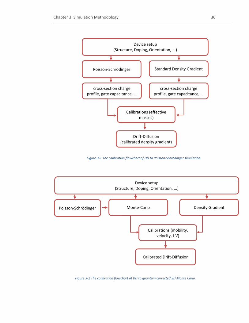
Chapter 3. Simulation Methodology 36
Standard Density Gradient Poisson-Schrödinger
Device setup (Structure, Doping, Orientation, ...)
cross-section charge profile, gate capacitance, …
…
cross-section charge profile, gate capacitance, …
Calibrations (effective masses)
Drift-Diffusion (calibrated density gradient)
Figure 3-1 The calibration flowchart of DD to Poisson-Schrödinger simulation.
Figure 3-2 The calibration flowchart of DD to quantum corrected 3D Monte Carlo.
Device setup (Structure, Doping, Orientation, ...)
Poisson-Schrödinger Density Gradient Monte-Carlo
Calibrations (mobility, velocity, I-V)
Calibrated Drift-Diffusion
Chapter 3. Simulation Methodology 37
Drift Diffusion
Near equilibrium device physics and behaviour are primarily modelled using the drift
diffusion (DD) approach. The DD method is suitable when the devices are of an adequate
size to discount quantum effects, and for long-channel devices that are not rapidly switched.
Whilst one of the main benefits of the model is its straightforward implementation, resulting
in widespread adoption, it is incapable of capturing nonequilibrium transport effects. The
DD method works based on the assumption that carriers are in thermal equilibrium, and
although field-dependent diffusivities and mobilities can be used, the assumption is that
these parameters can react immediately to any electric field fluctuation. This assumption is
inaccurate for smaller devices, wherein the transport variables are not directly correlated to
the local electric field. Additionally, the classic DD method cannot capture velocity
overshoot [90] and other non-local effects. Furthermore, the DD model can provide highly
inaccurate representations of charge velocity distribution, potential configuration, and
charge density in aggressively scaled transistors. Thus, the DD approach is often unsuitable
for exploring the in-depth physics of short-channel devices during simulation [91], [92].
The DD method is based the Poisson’s equation (a fundamental electrostatics equation based
on the Maxwell equation), current transport equations for electrons and holes in drift-
diffusion approximation (derived from Boltzmann’s transport equation) implemented in the
current continuity equation. The above equations are solved self-consistently using
numerical techniques. The DD equations are outlined in further detail in the following
sections.
3.2.1 Maxwell's equations
The differential-form of Maxwell's equations are;
I. Gauss's law of electrostatics:
∇. 𝐷 = 𝜌 , ∇. 𝐸 = −𝜌
𝜖𝜊 (3-1)
II. Gauss's law for magnetism:
∇. 𝐵 = 0 (3-2)
III. Faraday's law of induction:
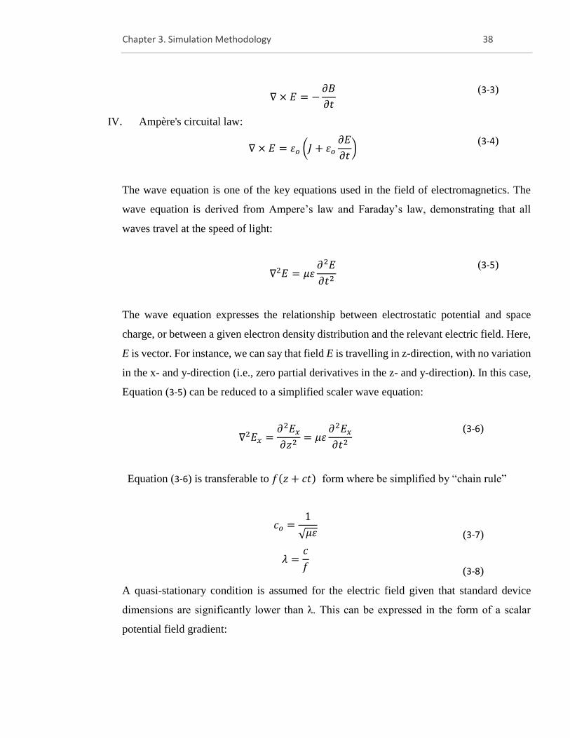
Chapter 3. Simulation Methodology 38
∇ × 𝐸 = −
𝜕𝐵
𝜕𝑡
(3-3)
IV. Ampère's circuital law:
∇ × 𝐸 = 휀𝜊 (𝐽 + 휀𝜊
𝜕𝐸
𝜕𝑡)
(3-4)
The wave equation is one of the key equations used in the field of electromagnetics. The
wave equation is derived from Ampere’s law and Faraday’s law, demonstrating that all
waves travel at the speed of light:
∇2𝐸 = 𝜇휀
𝜕2𝐸
𝜕𝑡2
(3-5)
The wave equation expresses the relationship between electrostatic potential and space
charge, or between a given electron density distribution and the relevant electric field. Here,
E is vector. For instance, we can say that field E is travelling in z-direction, with no variation
in the x- and y-direction (i.e., zero partial derivatives in the z- and y-direction). In this case,
Equation (3-5) can be reduced to a simplified scaler wave equation:
∇2𝐸𝑥 =
𝜕2𝐸𝑥
𝜕𝑧2= 𝜇휀
𝜕2𝐸𝑥
𝜕𝑡2
(3-6)
Equation (3-6) is transferable to 𝑓(𝑧 + 𝑐𝑡) form where be simplified by “chain rule”
𝑐𝑜 =
1
√𝜇휀
(3-7)
𝜆 =
𝑐
𝑓
(3-8)
A quasi-stationary condition is assumed for the electric field given that standard device
dimensions are significantly lower than λ. This can be expressed in the form of a scalar
potential field gradient:
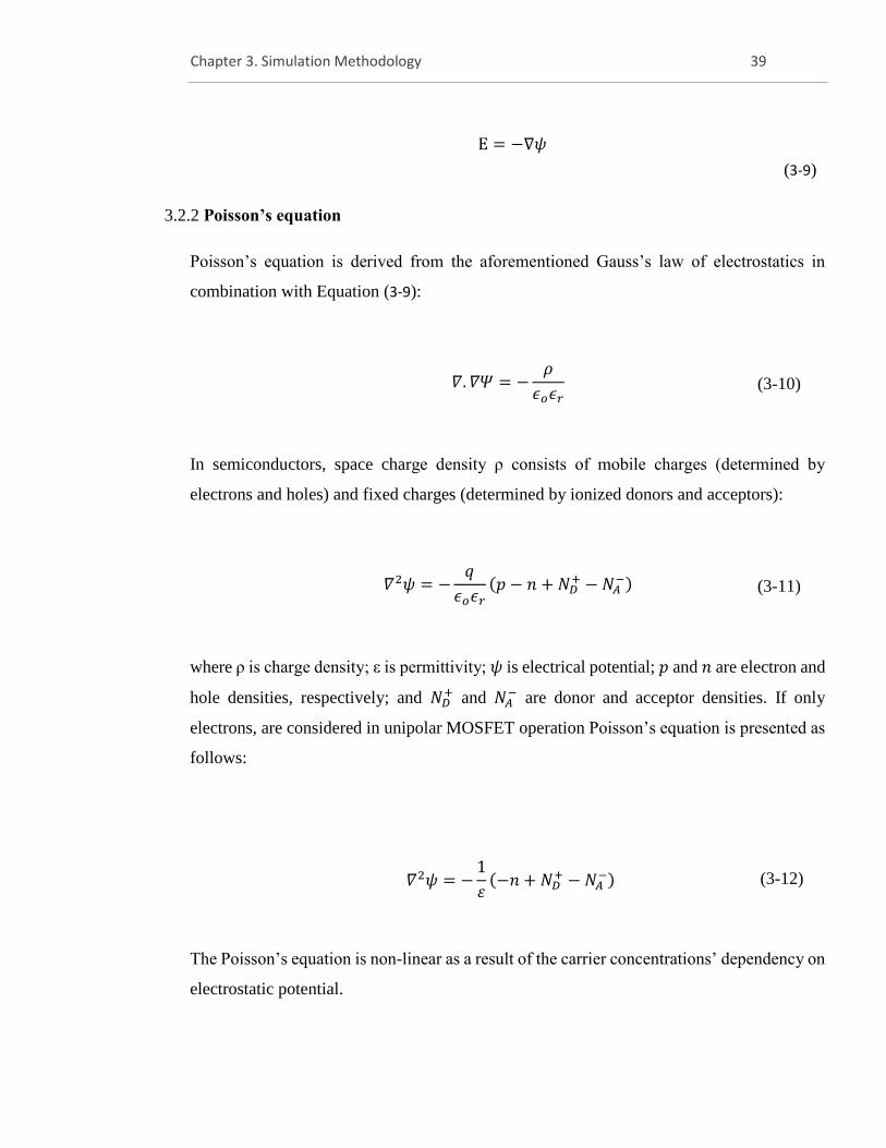
Chapter 3. Simulation Methodology 39
3.2.2 Poisson’s equation
Poisson’s equation is derived from the aforementioned Gauss’s law of electrostatics in
combination with Equation (3-9):
𝛻. 𝛻𝛹 = −𝜌
𝜖𝜊𝜖𝑟 (3-10)
In semiconductors, space charge density ρ consists of mobile charges (determined by
electrons and holes) and fixed charges (determined by ionized donors and acceptors):
𝛻2𝜓 = −𝑞
𝜖𝜊𝜖𝑟
(𝑝 − 𝑛 + 𝑁𝐷+ − 𝑁𝐴
−) (3-11)
where ρ is charge density; ε is permittivity; 𝜓 is electrical potential; 𝑝 and 𝑛 are electron and
hole densities, respectively; and 𝑁𝐷+ and 𝑁𝐴
− are donor and acceptor densities. If only
electrons, are considered in unipolar MOSFET operation Poisson’s equation is presented as
follows:
The Poisson’s equation is non-linear as a result of the carrier concentrations’ dependency on
electrostatic potential.
E = −∇𝜓
(3-9)
𝛻2𝜓 = −
1
휀(−𝑛 + 𝑁𝐷
+ − 𝑁𝐴−) (3-12)
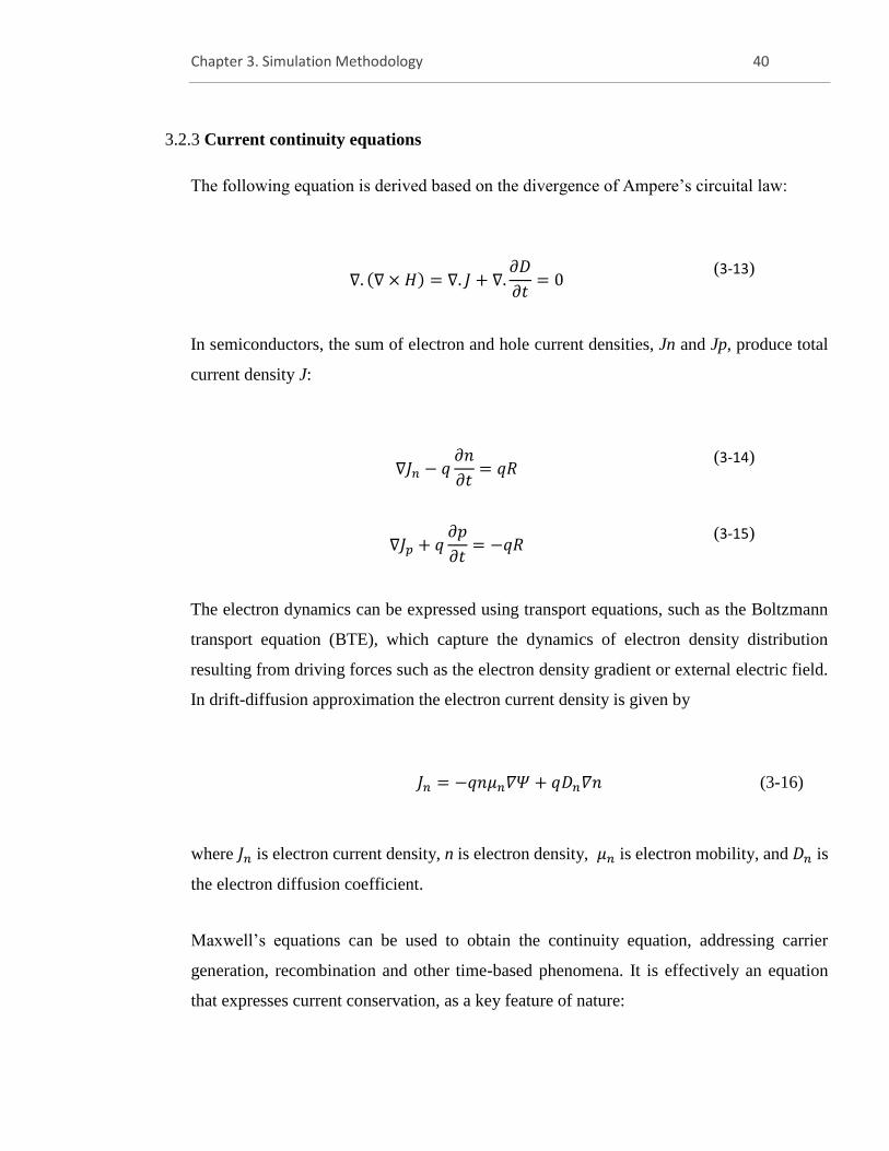
Chapter 3. Simulation Methodology 40
3.2.3 Current continuity equations
The following equation is derived based on the divergence of Ampere’s circuital law:
∇. (∇ × 𝐻) = ∇. 𝐽 + ∇.
𝜕𝐷
𝜕𝑡= 0
(3-13)
In semiconductors, the sum of electron and hole current densities, Jn and Jp, produce total
current density J:
∇𝐽𝑛 − 𝑞
𝜕𝑛
𝜕𝑡= 𝑞𝑅
(3-14)
∇𝐽𝑝 + 𝑞
𝜕𝑝
𝜕𝑡= −𝑞𝑅
(3-15)
The electron dynamics can be expressed using transport equations, such as the Boltzmann
transport equation (BTE), which capture the dynamics of electron density distribution
resulting from driving forces such as the electron density gradient or external electric field.
In drift-diffusion approximation the electron current density is given by
𝐽𝑛 = −𝑞𝑛𝜇𝑛𝛻𝛹 + 𝑞𝐷𝑛𝛻𝑛 (3-16)
where 𝐽𝑛 is electron current density, n is electron density, 𝜇𝑛 is electron mobility, and 𝐷𝑛 is
the electron diffusion coefficient.
Maxwell’s equations can be used to obtain the continuity equation, addressing carrier
generation, recombination and other time-based phenomena. It is effectively an equation
that expresses current conservation, as a key feature of nature:
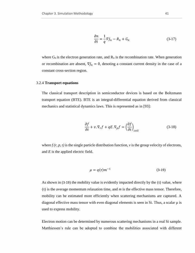
Chapter 3. Simulation Methodology 41
𝜕𝑛
𝜕𝑡=
1
𝑞𝛻𝐽𝑛 − 𝑅𝑛 + 𝐺𝑛 (3-17)
where Gn is the electron generation rate, and Rn is the recombination rate. When generation
or recombination are absent, ∇𝐽𝑛 = 0, denoting a constant current density in the case of a
constant cross-section region.
3.2.4 Transport equations
The classical transport description in semiconductor devices is based on the Boltzmann
transport equation (BTE). BTE is an integral-differential equation derived from classical
mechanics and statistical dynamics laws. This is represented as in [93]:
𝜕𝑓
𝜕𝑡+ 𝑣. ∇𝑟𝑓 + 𝑞𝐸. ∇𝑝𝑓 = (
𝜕𝑓
𝜕𝑡)
𝑐𝑜𝑙𝑙 (3-18)
where f (r, p, t) is the single particle distribution function, v is the group velocity of electrons,
and E is the applied electric field.
𝜇 = 𝑞⟨𝜏⟩𝑚−1 (3-19)
As shown in (3-19) the mobility value is evidently impacted directly by the ⟨τ⟩ value, where
⟨τ⟩ is the average momentum relaxation time, and m is the effective mass tensor. Therefore,
mobility can be estimated more efficiently when scattering mechanisms are captured. A
diagonal effective mass tensor with even diagonal elements is seen in Si. Thus, a scalar µ is
used to express mobility.
Electron motion can be determined by numerous scattering mechanisms in a real Si sample.
Matthiessen’s rule can be adopted to combine the mobilities associated with different
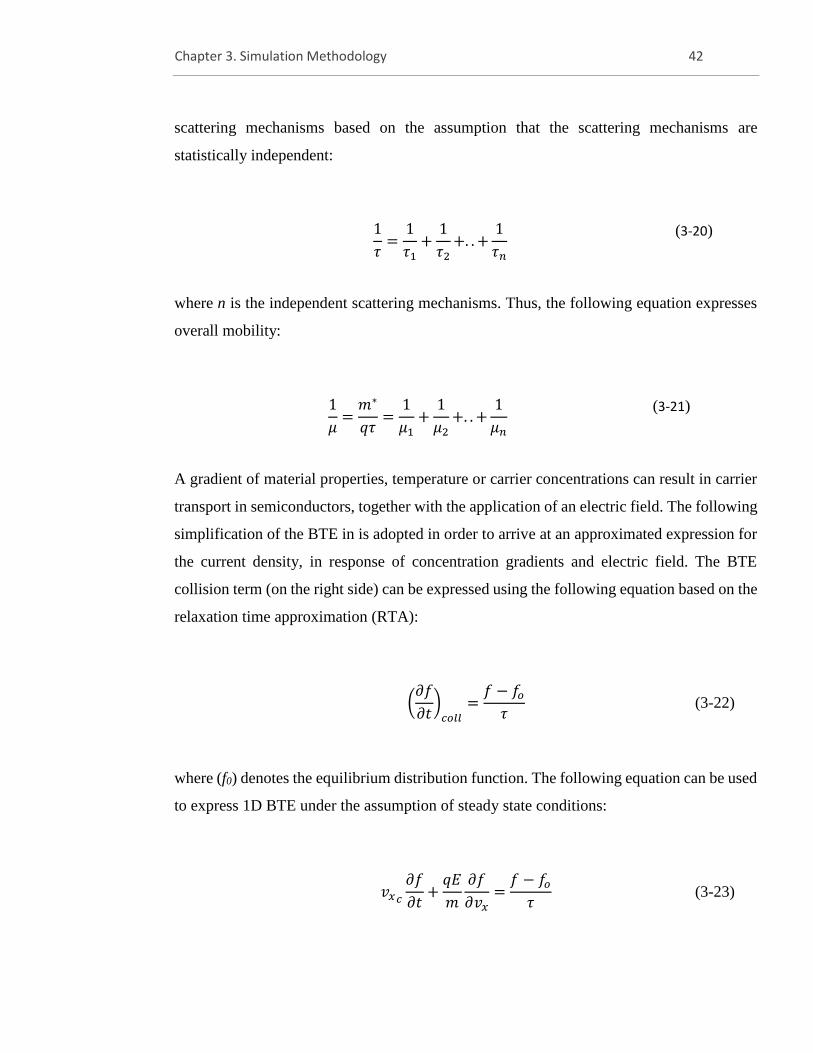
Chapter 3. Simulation Methodology 42
scattering mechanisms based on the assumption that the scattering mechanisms are
statistically independent:
1
𝜏=
1
𝜏1+
1
𝜏2+. . +
1
𝜏𝑛
(3-20)
where n is the independent scattering mechanisms. Thus, the following equation expresses
overall mobility:
1
𝜇=
𝑚∗
𝑞𝜏=
1
𝜇1+
1
𝜇2+. . +
1
𝜇𝑛
(3-21)
A gradient of material properties, temperature or carrier concentrations can result in carrier
transport in semiconductors, together with the application of an electric field. The following
simplification of the BTE in is adopted in order to arrive at an approximated expression for
the current density, in response of concentration gradients and electric field. The BTE
collision term (on the right side) can be expressed using the following equation based on the
relaxation time approximation (RTA):
(
𝜕𝑓
𝜕𝑡)
𝑐𝑜𝑙𝑙=
𝑓 − 𝑓𝜊
𝜏 (3-22)
where (f0) denotes the equilibrium distribution function. The following equation can be used
to express 1D BTE under the assumption of steady state conditions:
𝑣𝑥𝑐
𝜕𝑓
𝜕𝑡+
𝑞𝐸
𝑚
𝜕𝑓
𝜕𝑣𝑥=
𝑓 − 𝑓𝜊
𝜏 (3-23)
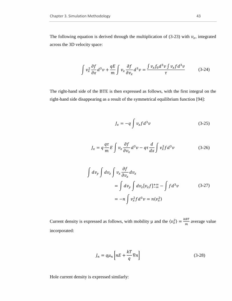
Chapter 3. Simulation Methodology 43
The following equation is derived through the multiplication of (3-23) with 𝑣𝑥, integrated
across the 3D velocity space:
∫ 𝑣𝑥
2𝜕𝑓
𝜕𝑥𝑑3𝑣 +
𝑞𝐸
𝑚∫ 𝑣𝑥
𝜕𝑓
𝜕𝑣𝑥𝑑3𝑣 =
∫ 𝑣𝑥𝑓0𝑑3𝑣 ∫ 𝑣𝑥𝑓𝑑3𝑣
𝜏 (3-24)
The right-hand side of the BTE is then expressed as follows, with the first integral on the
right-hand side disappearing as a result of the symmetrical equilibrium function [94]:
𝐽𝑥 = −𝑞 ∫ 𝑣𝑥𝑓𝑑3𝑣 (3-25)
𝐽𝑥 = 𝑞
𝑞𝜏
𝑚𝐸 ∫ 𝑣𝑥
𝜕𝑓
𝜕𝑣𝑥𝑑3𝑣 − 𝑞𝜏
𝑑
𝑑𝑥∫ 𝑣𝑥
2𝑓𝑑3𝑣 (3-26)
∫ 𝑑𝑣𝑦 ∫ 𝑑𝑣𝑧 ∫ 𝑣𝑥
𝜕𝑓
𝜕𝑣𝑥𝑑𝑣𝑥
= ∫ 𝑑𝑣𝑦 ∫ 𝑑𝑣𝑧[𝑣𝑥𝑓]−∞+∞ − ∫ 𝑓𝑑3𝑣
= −𝑛 ∫ 𝑣𝑥2𝑓𝑑3𝑣 = 𝑛⟨𝑣𝑥
2⟩
(3-27)
Current density is expressed as follows, with mobility µ and the ⟨𝑣𝑥2⟩ =
𝑘𝐵𝑇
𝑚 average value
incorporated:
𝐽𝑛 = 𝑞𝜇𝑛 [𝑛𝐸 +𝑘𝑇
𝑞∇𝑛] (3-28)
Hole current density is expressed similarly:
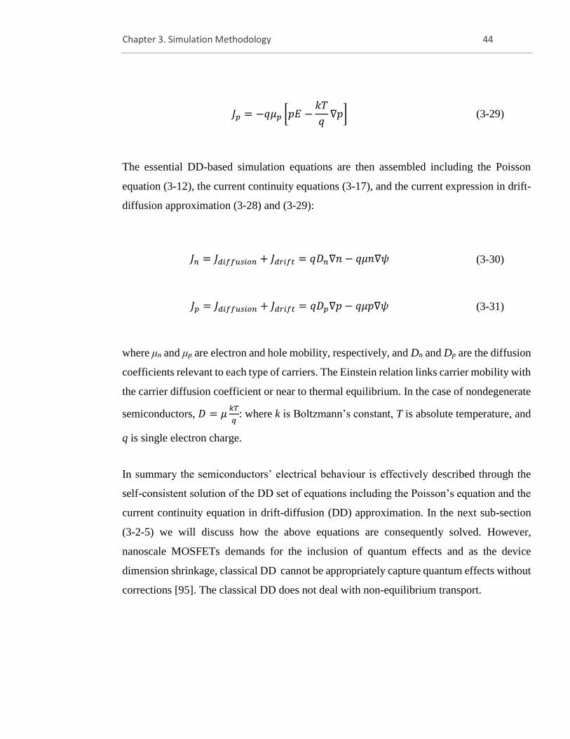
Chapter 3. Simulation Methodology 44
𝐽𝑝 = −𝑞𝜇𝑝 [𝑝𝐸 −𝑘𝑇
𝑞∇𝑝] (3-29)
The essential DD-based simulation equations are then assembled including the Poisson
equation (3-12), the current continuity equations (3-17), and the current expression in drift-
diffusion approximation (3-28) and (3-29):
𝐽𝑛 = 𝐽𝑑𝑖𝑓𝑓𝑢𝑠𝑖𝑜𝑛 + 𝐽𝑑𝑟𝑖𝑓𝑡 = 𝑞𝐷𝑛∇𝑛 − 𝑞𝜇𝑛∇𝜓 (3-30)
𝐽𝑝 = 𝐽𝑑𝑖𝑓𝑓𝑢𝑠𝑖𝑜𝑛 + 𝐽𝑑𝑟𝑖𝑓𝑡 = 𝑞𝐷𝑝∇𝑝 − 𝑞𝜇𝑝∇𝜓 (3-31)
where μn and μp are electron and hole mobility, respectively, and Dn and Dp are the diffusion
coefficients relevant to each type of carriers. The Einstein relation links carrier mobility with
the carrier diffusion coefficient or near to thermal equilibrium. In the case of nondegenerate
semiconductors, 𝐷 = 𝜇𝑘𝑇
𝑞: where k is Boltzmann’s constant, T is absolute temperature, and
q is single electron charge.
In summary the semiconductors’ electrical behaviour is effectively described through the
self-consistent solution of the DD set of equations including the Poisson’s equation and the
current continuity equation in drift-diffusion (DD) approximation. In the next sub-section
(3-2-5) we will discuss how the above equations are consequently solved. However,
nanoscale MOSFETs demands for the inclusion of quantum effects and as the device
dimension shrinkage, classical DD cannot be appropriately capture quantum effects without
corrections [95]. The classical DD does not deal with non-equilibrium transport.
Chapter 3. Simulation Methodology 45
3.2.5 Self-consistent calculation based on the Gummel’s method
In most cases, electron device simulation requires the solution of a self-consistent system of
equations describing the devices’ charge distribution and the electrostatic potential ψ. Self-
consistency occurs when flow of charge in the device is in equilibrium with the potential
distribution in the device, which in part is affected by the moving charges. Here, charge
density ρ adjusts when ψ is altered which in turns changes the potential, ‘self-consistency’
is reached when the charge and the potential reach equilibrium condition.
The achievement of self-consistency is essential for correctly obtaining the simulated
devices’ field distribution and current flow. In order to achieve this, we solve Poisson’s
equation and the current continuity equation simultaneously, which enables to determine the
correct mobile charge distribution and corresponding current (3-11).
The numerical solution of the DD set of equation is based on the self-consistent solution of
the electron density (n) and the electrostatic potential (ψ) as two unknown variables. Both
variables are position dependent. In the case of a MOSFET in absence of generation and
recombination the current continuity equation results in constant current density (J) along
the channel. The self-consistency in the Gummel approach is obtained by alternated
solutions of the Poisson and the current continuity equation. Typically, the solution for the
electron density n from the current continuity equation is based on the previous solution for
the electrostatic potential ψ. An updated ψ distribution is than obtained by applying the new
carrier concentration distribution n when solving again the Poisson’s equation. Convergence
is achieved if the new ψ distribution is sufficiently close to the previous ψ distribution. If
not, the iterations between the solution of the current continuity equation and the Poisson
equation continue. [96], [92].
The electrical characteristics of a single CMOS transistor can be simulated using the GSS
TCAD device simulator, GARAND. This is a DD simulator based on finite volume
discretisation of the Poisson and the current continuity equations. The self-consistency in
Garand is achieved using Gummel iterations (Figure 3-3). Additionally, GARAND also
considers the quantum mechanical confinement effects using the density gradient quantum
Chapter 3. Simulation Methodology 46
corrections approach. GARAND is a 3D simulator and arbitrary-shaped 3D MOSFET
structures can be simulated using GARAND.
3.2.6 Limitations of classical Drift-Diffusion approach
The DD approach has been adopted widely by the industry and was accurate in the
simulation of relatively large devices in above 100nm technology generations. The main
benefits of the DD approach in 2D and 3D simulation environment, its simplicity and its
computational efficiency. The DD method assumes local relation between carrier velocity
and the electric field, incapable to describe non-local effects based on the fact that the
velocity and energy at particular point depends on the field distribution along the particle
trajectory leading to the current position [90]. The DD method applied to contemporary and
future CMOS transistors is most suitable in the subthreshold region of the device operation
where the electrostatics plays a dominant role, and where there is a weak coupling between
the current continuity and the Poisson equation solution. Here, the channel contains only a
small amount of mobile charge due to the high source-to-drain potential barrier. Gate
voltage, drain voltage together with line-edge roughness (LER), interface roughness,
differences in dopant placement, and other barrier fluctuation sources determine the barrier
landscape [97]–[99]. It is well understood that DD is inaccurate in capturing on-current (Ion)
and the on-current variability in contemporary MOSFETS above the threshold level [100].
The assumptions that form the basis of DD equations are violated as the devices are scaled
to nanometre dimensions, resulting in a non-equilibrium and non-local transport problem.
Here, prior scattering along the carrier trajectories must be considered. The traditional DD
approach assumes that the carriers are in thermal equilibrium with the crystal lattice,
discounting the carrier heating and the non-equilibrium transport. The hot carriers arise due
to an increase in the electric field caused by the device scaling. Therefore, the DD approach
runs out of steam as the devices are scaled to nanometre dimensions, Non-local effects are
not represented by the DD simulation, since it only captures instant local velocity
modifications related to the local electric field. In small devices, field changes occur quickly,
with μn and Dn no longer related directly to the local electric field, and with carrier history
now a determining the velocity and the energy at particular point in the simulation domain.
Chapter 3. Simulation Methodology 47
In particular the DD simulation approach does not capture the carrier velocity overshoot
which is non-equilibrium transport phenomenon [101], arising as a result of the carriers
moving with velocity higher than the saturation velocity in the case of small devices with
rapidly varying electric field in the channel. The spatial velocity overshoot is a result of the
faster response in average carrier velocity with the average kinetic energy lagging when
carriers move from a low field a high field region in rapidly field changing conditions. Since
the DD approach is based on a simple field-dependent mobility model that is connected to
the electric field at a local level, the DD approach does not capture the velocity overshoot
[102]. Previous research indicates that velocity overshoot has beneficial impact on the
transistor performance, increasing drive current, transconductance and reducing circuit
switching time [103]. Higher order approximation to the BTE, where thermal equilibrium is
not assumed, including the energy transport equations and hydrodynamic set of equations
[104] can capture overshoot effects at greater computational expense. The need for more
accurate BTE solutions has been highlighted due the deficiencies of the DD and the
hydrodynamic approach in the simulation of extremely-scaled devices [104].
With the transistor scaling to nanometre dimensions there is a greater need to represent
accurately the quantum effects in the simulations. In particular in NWT FETs, the accurate
simulation of mobile charge and gate capacitance require quantum mechanical treatment.
Quantum corrections can be introduced into DD simulations. Methods based on the solution
of the Schrödinger equation are adopted in the research presented in this thesis. The
effective quantum potential extracted from the quantum solution is combined with the
classical potential (obtained by solving Poisson’s equation) providing the driving potential
that is used in the current continuity equation in the DD simulation, or for determining the
particles’ driving force in the MC simulations. A 2D Poisson-Schrödinger solver used in the
planes normal to the transport direction to provide the quantum charge distribution and the
associated effective quantum potential. Next section (section 3-3) will describe Poisson-
Schrödinger simulation.
Chapter 3. Simulation Methodology 48
Poisson-Schrödinger
The simulation of aggressively-scaled MOSFET requires the accurate inclusion of quantum
effects. Contemporary MOSFETs have a channel length close to the mean carrier free path,
with an oxide layer approximately three Si lattice interatomic atomic layers thick. In order
to improve the electrostatic control in NWTs, the gate completely surrounds the nanowire
channel on top of the gate oxide layer. Quantum confinement starts to play important role
when the nanowire diameter becomes smaller than 8nm. The self-consistent solution of the
Schrödinger and the Poisson equations in the 2D cross sectional plane of the NWT can
provide accurate description of the quantisation effects in the NWT channel. The potential
well in the NWTs is narrow leading to strong quantisation effects including sub band
splitting and affecting the shape of the carrier distribution in the channel, the ground state
(the lowest permitted electron energy level in the quantum well) is shifted above the bottom
of the conduction band resulting in threshold voltage shift. The 1D quantum transport
direction along the channel, surrounded by the gate, is perpendicular to the confinement
planes (2D) [105].
The quantum mechanical confinement has a significant impact on charge distribution. In
classical DD simulations the maximum of the inversion layer charge is at the interface, with
the charge density exponentially decreasing away from the interface. In reality the quantum
mechanical charge distribution peaks at a distance away from the interface. In NWTs the
quantum mechanical charge distribution results in volume inversion with the current flowing
dominantly in the middle of the NWT channel.
In GARAND the first-order quantum mechanical effects are taken into account using density
gradient quantum corrections. However, in this study a more sophisticated quantum
mechanical model is adopted, based on the self-consistent Poisson-Schrödinger (PS)
equation solutions. This offers more accurate description of the quantum mechanical effects,
at the expense of lower computational efficiency and greater computational times. Similarly,
to the DG simulation approach, the more accurate PS based quantum corrections are
implemented in the DD simulations using an iterative convergence scheme. The iterations
start with classical DD simulation. Once convergence is achieved, the DD solution is used
Chapter 3. Simulation Methodology 49
to determine the quasi-Fermi level, used as reference in the PS simulations and the initial
shape of the confinement potential in each discretisation plane normal to the transport
direction. The 2D quantum mechanical charge distribution in each 2D discretisation plane
is then obtained by solving self consistently the Poisson-Schrödinger equation in each
discretization plane. Figure 3-4 presents a flowchart of this simulation.
A quantum correction term is derived from the quantum mechanical charge distribution
obtained from the Schrödinger solution, and this term applied to the current density equation
in the next iteration of the DD system solution. The iterations between the DD and the PS
solutions are repeated until convergence. Figure 3-5 illustrates the secondary DD loop. The
same quantum correction term can also be used in simulations carried out using the Monte
Carlo method.
The Poisson and Schrödinger equations are solved in the 2D discretisation plane providing
the correct charge distribution and gate capacitance in the channel of the NWTs. The Poisson
equation (3-12) in this case includes the doping charge and the quantum mechanical charge
distribution acquired from the solution of the Schrödinger equation. The Schrödinger
equation in tensor effective mass approximation is given in the form:
−
ℎ2
2∇
1
𝑚𝑖𝑗∇𝜓 = (𝜓 − 𝐸)𝜓 (3-32)
The wavefunction is set to zero through the default setting of Dirichlet boundary conditions
to the outer bounds of the Schrödinger domain. In order to prevent the wavefunction entering
metallic regions, metals are also subject to the same boundary condition. The LAPACK
libraries’ numerical eigenvalue solver is applied to calculate the eigenvalues and the wave
functions. The solutions of the Schrödinger equation provide the wave functions in each
valley in the band structure within each of the 2d discretisation cross-sections. The total
mobile charge distribution is obtained as a sum of the charge distribution in each calculated
from the corresponding wave function distributions. The new potential value is then solved.
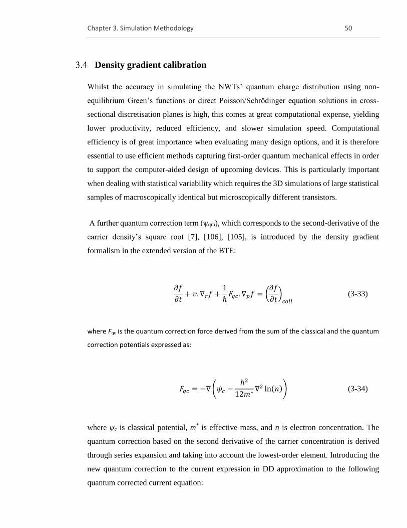
Chapter 3. Simulation Methodology 50
Density gradient calibration
Whilst the accuracy in simulating the NWTs’ quantum charge distribution using non-
equilibrium Green’s functions or direct Poisson/Schrödinger equation solutions in cross-
sectional discretisation planes is high, this comes at great computational expense, yielding
lower productivity, reduced efficiency, and slower simulation speed. Computational
efficiency is of great importance when evaluating many design options, and it is therefore
essential to use efficient methods capturing first-order quantum mechanical effects in order
to support the computer-aided design of upcoming devices. This is particularly important
when dealing with statistical variability which requires the 3D simulations of large statistical
samples of macroscopically identical but microscopically different transistors.
A further quantum correction term (ψqm), which corresponds to the second-derivative of the
carrier density’s square root [7], [106], [105], is introduced by the density gradient
formalism in the extended version of the BTE:
𝜕𝑓
𝜕𝑡+ 𝑣. ∇𝑟𝑓 +
1
ℏ𝐹𝑞𝑐. ∇𝑝𝑓 = (
𝜕𝑓
𝜕𝑡)
𝑐𝑜𝑙𝑙 (3-33)
where Fqc is the quantum correction force derived from the sum of the classical and the quantum
correction potentials expressed as:
𝐹𝑞𝑐 = −∇ (𝜓𝑐 −
ℏ2
12𝑚∗∇2 ln(𝑛)) (3-34)
where ψc is classical potential, m* is effective mass, and n is electron concentration. The
quantum correction based on the second derivative of the carrier concentration is derived
through series expansion and taking into account the lowest-order element. Introducing the
new quantum correction to the current expression in DD approximation to the following
quantum corrected current equation:
Chapter 3. Simulation Methodology 51
𝐽𝑛 = 𝑞𝐷𝑛∇𝑛 − 𝑞𝜇𝑛n∇𝜓 + 2𝜇𝑛∇ (𝑏𝑛
∇2√𝑛
√𝑛) (3-35)
𝑏𝑛 =ℏ2
4𝑞𝑚∗𝑟
where r is a fitting parameter taking values between 1 and 3, based on the number of
occupied sub-bands.
In many cases, first-order quantum corrections are implemented through a so-called
effective quantum potential. Here, a quantum correction term is applied to adjust the
electrostatic potential used in traditional simulation methods. This allows the necessary
quantum mechanical effects to be modelled, therefore maintaining the stability of the
simulator and its computational efficiency.
As noted, a further the quantum correction term ψqm, which corresponds to the second-
derivative of the carrier density’s square root, can be obtained using the density gradient
(DG) formalism. The effective quantum potential ψqm is related to the quasi-Fermi level 𝛷𝑛
by the following equation:
𝜓𝑞𝑚 = 2𝑏𝑛
𝛻2√𝑛
√𝑛= 𝛷𝑛 − 𝛹 +
𝑘𝐵𝑇
𝑞𝑙𝑛 (
𝑛
𝑛𝑖) (3-36)
𝑏𝑛 =ℏ2
12𝑞𝑚𝑛
where bn is a parameter, which can be calibrated to replicate the electron distribution
obtained usually from self-consistent Poisson-Schrödinger (PS) simulations. Figure 3-3
presents a standard DD simulation flowchart incorporating density gradient quantum
corrections.
Chapter 3. Simulation Methodology 52
𝜓𝑞𝑚 = 2𝑏𝑛
𝛻2√𝑛
√𝑛= 𝛷𝑛 − 𝛹 +
𝑘𝐵𝑇
𝑞𝑙𝑛 (
𝑛
𝑛𝑖) (3-37)
Effective mass is used as a fitting parameter, with the density gradient equation calibration
3-38 solved numerically and calibrated against the results of Poisson-Schrödinger solution.
With the assumption that the density gradient effective mass is anisotropic, with different
effective mass components of the principle direction (mx, my and mz) the DG equation can
be written in the following form:
2𝑏𝑛
𝑆(
1
𝑚𝑥
𝜕2𝑆
𝜕𝑥2+
1
𝑚𝑦
𝜕2𝑆
𝜕𝑦2+
1
𝑚𝑧
𝜕2𝑆
𝜕𝑧2)
= 𝜙𝑛 − 𝜓 +𝑘𝐵𝑇
𝑞𝑙𝑛 (
𝑆2
𝑛𝑖)
(3-38)
where 𝑏𝑛 = ℏ2/12𝑞, and 𝑆 = √𝑛. The charge distributions derived from the Poisson-
Schrödinger solutions along the NWT cross-section’s major and minor axes are used as the
basis for calibrating the conduction band density gradient effective masses in the silicon and
in the oxide.
To secure charge neutrality being maintaining taking into account the impact of the
electrostatic potential on the electron injection, Neumann boundary conditions (NBCs) are
adopted in the source and drain when implementing NEGF simulation approach and other
quantum mechanical transport methods. Whilst most DD simulators use the Dirichlet
boundary conditions for the potential at the ohmic S/D contacts, NBCs are also employed in
GARAND to allow for the consistent application of the DG quantum corrections. NBCs are
well suited for DG quantum corrections because they allow the correct quantum mechanical
charge distribution to be maintained in the source/drain regions. This is especially important
Chapter 3. Simulation Methodology 53
in the case of NWTs, FinFETs, and FDSOI transistors. Where implementations of the DG
approach, care should be taken when applying the quantum potential boundary conditions
at the interface between the semiconductor and the oxide. The approach described in [107]
adopted in GARAND to take into account the wave function penetration in the oxide. Using
this approach, the gradient of the electron concentration perpendicular to the
semiconductor/oxide interface is influenced by the effective masses in the two media. The
calculation of electron density penetration, as a function of distance (x) from the
semiconductor/oxide interface, is as described by the following expression:
𝑛(𝑥) = 𝑛(0)𝑒𝑥𝑝 (−
2𝑥
𝑥𝑝) (3-39)
where n(0) is electron density at the interface, and xp is penetration depth, derived from the
Wentzel-Kramers-Brillouin (WKB) equation:
𝑥𝑝 = −
ℏ
√2𝑚𝑜𝑥Φ𝐵
(3-40)
where mox is the oxide’s electron effective mass, and ΦB is the oxide’s potential barrier.
Based on Eqn. (3-37), the component 𝑏𝑛∇√𝑛 set normally to the semiconductor/oxide
interface can be expressed as:
𝑛. 𝑏𝑛∇𝑝√𝑛 = − (
𝑏𝑜𝑥
𝑥𝑝) √𝑛 (3-41)
where box is expressed as:
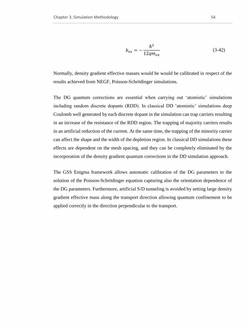
Chapter 3. Simulation Methodology 54
𝑏𝑜𝑥 = −
ℏ2
12𝑞𝑚𝑜𝑥 (3-42)
Normally, density gradient effective masses would be would be calibrated in respect of the
results achieved from NEGF, Poisson-Schrödinger simulations.
The DG quantum corrections are essential when carrying out ‘atomistic’ simulations
including random discrete dopants (RDD). In classical DD ‘atomistic’ simulations deep
Coulomb well generated by each discrete dopant in the simulation can trap carriers resulting
in an increase of the resistance of the RDD region. The trapping of majority carriers results
in an artificial reduction of the current. At the same time, the trapping of the minority carrier
can affect the shape and the width of the depletion region. In classical DD simulations these
effects are dependent on the mesh spacing, and they can be completely eliminated by the
incorporation of the density gradient quantum corrections in the DD simulation approach.
The GSS Enigma framework allows automatic calibration of the DG parameters to the
solution of the Poisson-Schrödinger equation capturing also the orientation dependence of
the DG parameters. Furthermore, artificial S/D tunneling is avoided by setting large density
gradient effective mass along the transport direction allowing quantum confinement to be
applied correctly in the direction perpendicular to the transport.
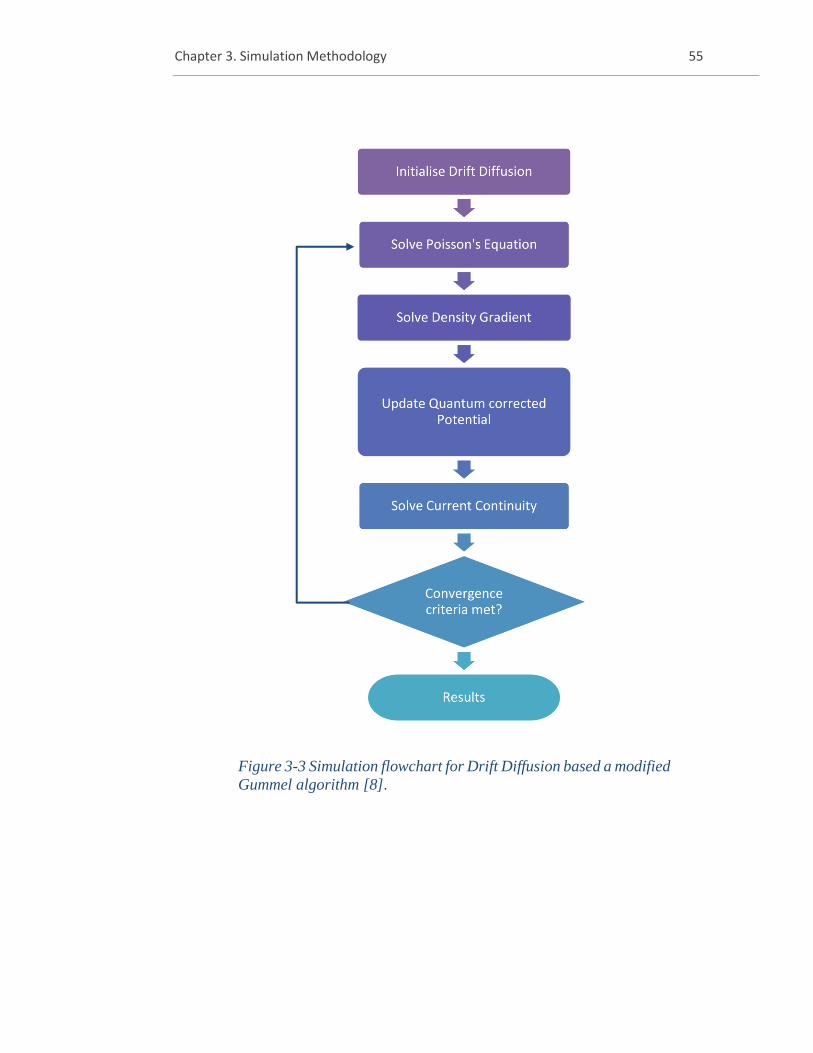
Chapter 3. Simulation Methodology 55
Figure 3-3 Simulation flowchart for Drift Diffusion based a modified
Gummel algorithm [8].
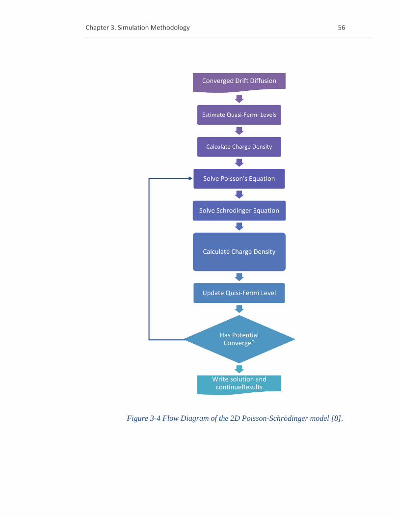
Chapter 3. Simulation Methodology 56
Figure 3-4 Flow Diagram of the 2D Poisson-Schrödinger model [8].
Chapter 3. Simulation Methodology 57
Figure 3-5 Flow diagram of the fixed Schrödinger quantum
correction DD model [8].
Chapter 3. Simulation Methodology 58
Monte Carlo
MC allows different parameterisations for electrons with different energy levels and thus it
is more flexible in allowing integration of Poisson-Schrodinger. In this section, we will
investigate on normal Monte Carlo first. The Monte Carlo method applied to semiconductor
device simulations provides a direct solution to the BTE. It provides and accurate solution
for the energy and momentum distribution in the presence of strong external electric field
leading to nonequilibrium transport effects. The solutions consider all relevant scattering
mechanisms, in a 2D/3D simulation domain which could be a very realistic representation
of the simulated device. The Monte Carlo approach simulates the effects of random
scattering events and the free flight carrier trajectories in electric field, bridging the classical
Newtonian mechanics and quantum mechanical scattering rates to provide a numerical
solution to the BTE.
Figure 3-6 illustrates a common simulation flow for an Ensemble Monte Carlo simulation
engine. The initialisation of the MC simulations proceeds by introducing MC super particles
into the solution domain according to the carrier density distribution obtained from DD
simulations. The energy dependent total scattering rate is calculated based on all relevant
scattering mechanisms. A random number in connection with the total scattering rate is then
used to determine a ‘free flight’ time for each super particle. During the free flight period
carriers move following classical lows of motion accelerated by the electric field. At the end
of the free flight an additional random number is used to select the scattering mechanism,
which is introduced once the free flight period ends. Here, the relevant scattering probability
distributions along with the choice of the superparticle state following scattering event
enable the device physics to be accurately reproduced by the MC simulations. Self-scattering
is also introduced leading to a constant total scattering rate, in order to simplified the flight
time selection process. Self-scattering is the most commonly-selected scattering
mechanisms in the majority of cases reducing the efficiency of the MC simulations. Statistics
are collected after scattering, with average values obtained, for particle velocity (3-43) and
energy (3-44) taking into account the nonparabolic band dispersion, described by
nonparabolicity factor. Using the expressions below.
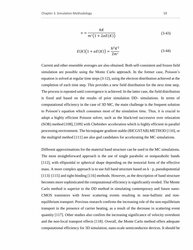
Chapter 3. Simulation Methodology 59
𝑣 =ℏ𝐾
𝑚∗(1 + 2𝛼𝐸(𝐾)) (3-43)
𝐸(𝐾)(1 + 𝛼𝐸(𝐾)) =ℏ2𝐾2
2𝑚∗ (3-44)
Current and other ensemble averages are also obtained. Both self-consistent and frozen field
simulation are possible using the Monte Carlo approach. In the former case, Poisson’s
equation is solved at regular time steps (3-12), using the electron distribution achieved at the
completion of each time step. This provides a new field distribution for the next time step.
The process is repeated until convergence is achieved. In the latter case, the field distribution
is fixed and based on the results of prior simulation DD- simulations. In terms of
computational efficiency in the case of 3D MC, the main challenge is the frequent solution
to Poisson’s equation which consumes most of the simulation time. Thus, it is crucial to
adopt a highly efficient Poisson solver, such as the black/red successive over relaxation
(SOR) method [108], [109] with Chebishev acceleration which is highly efficient in parallel
processing environment. The biconjugate gradient-stable (BICGSTAB) METHOD [110], or
the multigrid method [111] are also god candidates for accelerating the MC simulations.
Different approximations for the material band structure can be used in the MC simulations.
The most straightforward approach is the use of single parabolic or nonparabolic bands
[112], with ellipsoidal or spherical shape depending on the tensorial form of the effective
mass. A more complex approach is to use full band structure based on k · p, pseudopotential
[113]–[115] and tight-binding [116] methods. However, as the description of band structure
becomes more sophisticated the computational efficiency is significantly eroded. The Monte
Carlo method is superior to the DD method in simulating contemporary and future nano-
CMOS transistors with fewer scattering events resulting in near-ballistic and non-
equilibrium transport. Previous research confirms the increasing role of the non-equilibrium
transport in the presence of carrier heating, as a result of the decrease in scattering event
quantity [117]. Other studies also confirm the increasing significance of velocity overshoot
and the non-local transport effects [118]. Overall, the Monte Carlo method offers adequate
computational efficiency for 3D simulation, nano-scale semiconductor devices. It should be
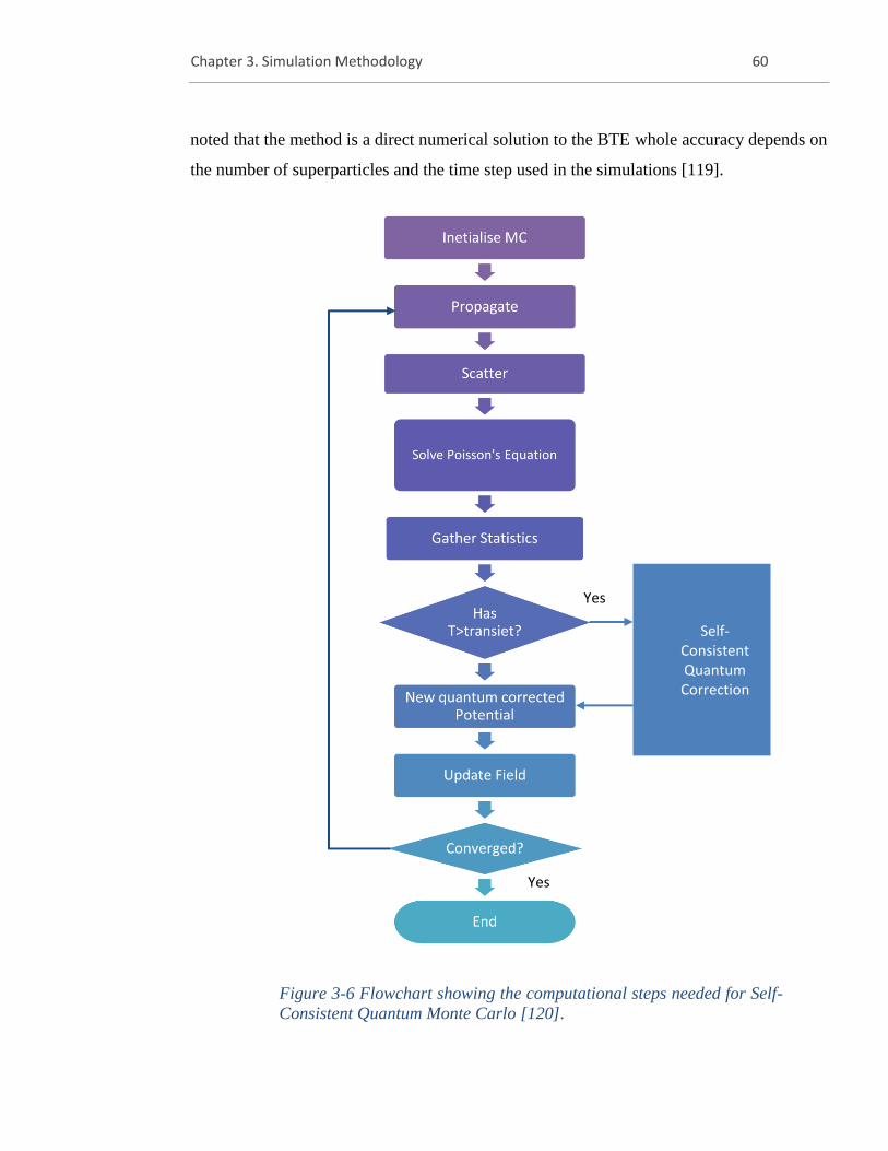
Chapter 3. Simulation Methodology 60
noted that the method is a direct numerical solution to the BTE whole accuracy depends on
the number of superparticles and the time step used in the simulations [119].
Figure 3-6 Flowchart showing the computational steps needed for Self-
Consistent Quantum Monte Carlo [120].
Self-Consistent Quantum Correction
Yes
Yes
Chapter 3. Simulation Methodology 61
Scattering in Monte Carlo
In order to accurately represent drive current variations and magnitude along with
electrostatic effects, which primarily impact threshold voltage and sub-threshold current, it
is crucial to introduce the relevant scattering processes into the Monte Carlo simulation.
However, this requires consideration of the trade-off with physical accuracy and
computational efficiency. The most common approach taken to achieve this is random
number selection, which determines the scattering process employed in the simulation via a
comparison table of the probabilities associated with each process [120]. Fermi’s golden
rule (3-45), (obtained through the Schrödinger equation) provides the probability of
perturbation Hamiltonian Hk',k leading to a shift between state k and k' (S(k, k')):
𝑆(𝑘, 𝑘′) =2𝜋
ℏ|𝐻𝑘′,𝑘|
2𝛿[𝐸(𝑘′) − 𝐸(𝑘)] (3-45)
The scattering probabilities associated with each process, as derived from the above
equation, are then tabulated, enabling the calculation of the total scattering rate and the
selection of the particular scattering process at the end of the free flight. This approach is
adopted for example for calculating acoustic and optical phonon scattering rates [112], as
well as scattering rates for ionised impurities and interface roughness [121]. The simulation
of the interface roughness scattering can also be achieved by using an alternative approach,
wherein specular or diffusive reflection [122] is introduced through weighted selection
[123]. However, the limitation of this approach is that it depends on a the selection of the
specular-diffusive scattering ratio which is device specific [124].
A new final state is randomly selected post-scattering. The randomly selected scattering
mechanism determines the modification of the particle’s energy, direction and magnitude
and direction of the momentum (k-vector). Numerous studies discuss the selection methods
used for each of the individual scattering mechanisms.
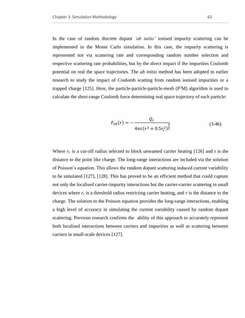
Chapter 3. Simulation Methodology 62
In the case of random discrete dopant ‘ab initio’ ionised impurity scattering can be
implemented in the Monte Carlo simulation. In this case, the impurity scattering is
represented not via scattering rate and corresponding random number selection and
respective scattering rate probabilities, but by the direct impact if the impurities Coulomb
potential on real the space trajectories. The ab initio method has been adopted in earlier
research to study the impact of Coulomb scatting from random ionised impurities or a
trapped charge [125]. Here, the particle-particle-particle-mesh (P3M) algorithm is used to
calculate the short-range Coulomb force determining real space trajectory of each particle:
𝐹𝑆𝑅(𝑟) = −
𝑄𝑟
4𝜋휀(𝑟2 + 0.5𝑟𝑐2)
32
(3-46)
Where rc is a cut-off radius selected to block unwanted carrier heating [126] and r is the
distance to the point like charge. The long-range interactions are included via the solution
of Poisson’s equation. This allows the random dopant scattering induced current variability
to be simulated [127], [128]. This has proved to be an efficient method that could capture
not only the localised carrier-impurity interactions but the carrier-carrier scattering in small
devices where rc is a threshold radius restricting carrier heating, and r is the distance to the
charge. The solution to the Poisson equation provides the long-range interactions, enabling
a high level of accuracy in simulating the current variability caused by random dopant
scattering. Previous research confirms the ability of this approach to accurately represent
both localised interactions between carriers and impurities as well as scattering between
carriers in small-scale devices [127].
Chapter 3. Simulation Methodology 63
Quantum Corrections in Monte Carlo
The incorporation of quantum corrections into the Monte Carlo simulation method enables
the accurate simulation of quantum confinement effects which play important role
determining the performance of nano-CMOS transistors. The quantum-corrected Monte
Carlo method provides accurate simulation results in highly-scaled devices with tSi thickness
in the range of 10 - 7 nm [129]–[133]. Therefore, the incorporation of quantum corrections
into the Monte Carlo model both upholds the approach’s computational efficiency and
enables tunnelling and size quantisation effects to be captured. Different methods have been
used to introduce quantum corrections in the MC simulations including the solution of the
Schrödinger [134], [135] and Wigner [136] equations, as well as by using effective
potentials derived from accurate quantum simulations or related to the DG approach [119],
[137], [138]. The standard method introduces quantum-correction potential (ψq) as follows:
𝜓𝑞 = 𝜓𝑐 + 𝜓𝑞𝑐 (3-47)
where ψc is classical potential (derived from the solution to Poisson’s equation), and ψqc is
quantum-corrected potential (derived via the methods outlined below). rather than
integrating the quantum-correction potential with the current continuity equation, as in the
case of DD simulation, quantum-corrected potential is instead utilised to determine the force
(F) impacting particles during the free flight period under the Monte Carlo method:
𝐹 = 𝐹𝑐 + 𝐹𝑞𝑐 (3-48)
𝐹𝑐 = −∇𝜓𝑐 (3-49)
𝐹𝑞𝑐 = −∇𝜓𝑞𝑐 (3-50)
Chapter 3. Simulation Methodology 64
Compared to quantum transport simulations, which offer greater accuracy and detail at high
computational expense, the introduction of quantum correction into semi-classical transport
offers greater efficiency, particularly given that PS equations are typically solved in the cross
sectional discretisation lanes once in only few times during the 3D Monte Carlo simulations
[139]. This is the most accurate method used to introduce quantum corrections in GARAND
MC engine. Alternatively, the DG method can be used for introducing the quantum
correction force in GARAND MC. In this case the calibrated DG quantum correction
method is used in the DD simulations used for initialisation of the MC simulations. The
mobile charge distribution at the end of the DD simulations is used to obtained ψqc
In the case of two-dimensional Monte Carlo simulation, a previous study presents a method
for incorporating the Poisson- Schrödinger solution into the model with greater efficiency
[139]. Here, periodic solutions to the Schrödinger equation are calculated, with a
perturbative method used to calculate eigen energies during the remaining time steps. In
other research, a Wigner distribution function-based correction term has also been presented
[136]. This is expressed as follows [140], beginning with the Wigner transport equation, as
a modified BTE:
𝜓𝑞 = 𝜓𝑐 +ℏ2
4𝑚∗𝑟𝑘𝐵𝑇[∇2𝜓𝑞 −
1
2𝑘𝐵𝑇(𝜓𝑞)
2] (3-51)
Calculating the solution to the above equation is challenging given its highly non-linear
structure. This being said, compared to the earlier approach, Eqn. (3-51) provides the benefit
of lower noise sensitivity. Previous research has confirmed the effectiveness of the
correction term in two-dimensional Monte Carlo simulations. Additionally, other studies
have adopted the method and applied it to incorporate numerous valleys’ electron
distribution [140], with the equation also applied beyond the thermal equilibrium
assumption. Both two-dimensional and three-dimensional Monte Carlo simulations have
been carried out in the literature using the effective potential method to accurately capture
confinement effects. Additionally, with multi gate MOSFETs, the method has also been
Chapter 3. Simulation Methodology 65
adopted to explore surface roughness scattering [141]. A scattering rate must be used to
ensure accuracy in modelling whilst also overcoming the limitation of the effective potential
method, in that it overestimates the degree to which carriers are turned away from the
interface. Thus, the selection of a weighted specular/diffusion reflection is unsuitable in this
case. The method has also been used to explore Coulomb interactions with unintended
doping [142], with dopant channel placement being found to be effective in capturing
degradation.
The adoption of the fitting parameter poses a noteworthy limitation to the method, however
[142]. When the field is overestimated, the interface’s electron concentration is
underestimated, resulting in the peak concentration moving away from the interface. In
comparison with Poisson-Schrödinger solutions, if the parameter is reduced in order to
correct this issue, this can result in a lower correction term than anticipated, along with a
peak concentration that is too high. The fitting parameter values must be varied in the normal
and parallel directions to the interface when the method is applied in 3D simulation.
The replacement of the Gaussian distribution with a Pearson IV distribution has been carried
out in order to present an alternative effective potential approach. Depending on the distance
between the carrier and semiconductor-oxide interface, the Pearson distribution can be tuned
at different points in the vertical direction. This is achieved using four parameters, rather
than the single parameter used in the Gaussian approach. The benefit of this method is
greater consistency with the Poisson-Schrödinger solution-based electron distribution [142].
However, validation and implementation of this method has only been achieved in 2D
simulation to date, with no extensive simulation research adopting the approach. The
following equation can be used to obtain a more computationally efficient Schrödinger-
based correction term, compared to the incorporation of a PS-based solution into Monte
Carlo simulation:
Chapter 3. Simulation Methodology 66
𝜓𝑞(𝑧) = −𝑘𝐵𝑇 log (𝑛𝑞(𝑧)) − 𝜓𝑐(𝑧) + 𝑉0 (3-52)
where nq(z) is quantum density (derived from the solution to the Schrödinger equation)
[134]. Here, nq(z) does not reflect values, but distribution shape. Quantum density is
calculated by periodically applying the eigenvalue solver to slices along the quantisation
direction, which upholds self-consistency. The correction term expressed in Eqn. (3-52) is
modified based on the result, although the solution to the Poisson equation is reached
separately based on the Monte Carlo electron distribution. This allows the simulation to
achieve the same computational efficiency as traditional models. This approach does not
require consideration of the Fermi level, since it only requires the quantum carrier density
shape. The method can be applied beyond the assumption of thermal equilibrium by means
of the varying carrier temperatures between the slices. Additionally, consistency with the
solution to the Poisson- Schrödinger is achieved due to the method’s adoption of the
Schrödinger solution. Both two-dimensional [143], [144] and three-dimensional [143],
[145], [146] applications of the method have been carried out, with correction and transport
being two- and three- dimensional, respectively. In both cases, a good level of accuracy has
been found in terms of size quantisation. However, the method has been found to be
unsuitable for capturing tunnelling effects [147].
Mobility and I-V calibration
One of the key parameters impacting semiconductor device performance in DD simulations
is the carrier mobility (μ). The dependence of mobility with the field (mobility models) has
traditionally been the way that DD simulations have been parameterised and calibrated to
correctly match theoretical results with experiment. There is a strong correlation between
the drive current and the mobility, with the drive current increasing as mobility increases.
Since scattering mechanisms such as surface roughness, lattice/phonon and ionised impurity
scattering have an impact on mobility, the accurate representation of carrier mobility
Chapter 3. Simulation Methodology 67
requires the key scattering mechanisms to be taken into account. Matthiessen’s rule (3-20)
is used when multiple scattering mechanisms are introduced in the mobility models.
The carrier mobility is reduced by ionised donor/acceptor-induced impurity scattering in
doped semiconductors. A typical mobility model in DD simulations has three components
including low-field mobility model, perpendicular-field mobility dependence and lateral-
field mobility dependence. There is a large variety of mobility models used in DD
simulations with different level of complexity and sometimes the low field mobility and the
field dependency cannot be clearly separate.
The low-field mobility model is further educed by the perpendicular-field model. The
combination of the two models determine the ID-VG characteristics of the CMOS transistor
at low drain bias. At high drain bias the mobility if further reduced by the lateral-field
mobility model which accounts for the velocity saturation effects at high electric field. The
three mobility models used in this study are explained in further detail below.
Low field mobility dependence
The low-field mobility value determines the base mobility mainly determined by the phonon
and the impurity scattering. Near the interface the low filed mobility is modified to take into
account the impact of the interface on the mobility in the MOSFET channel. It can also be
modified by the strain used to enhance the performance of contemporary CMOS transistors.
The Masetti (concentration-dependent) [148], Arora [149] (concentration-dependent) or
Philips [150] (concentration-dependent, including screening effects) mobility models are
available for selection in the atomistic simulator GARAND.
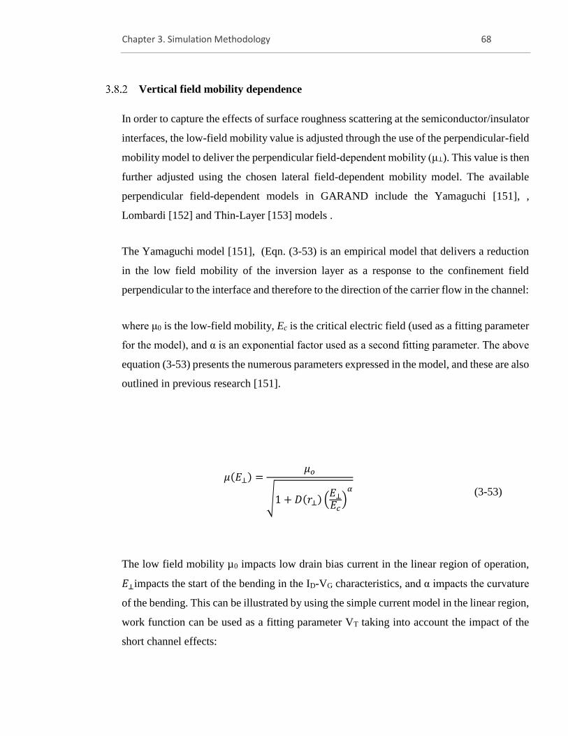
Chapter 3. Simulation Methodology 68
Vertical field mobility dependence
In order to capture the effects of surface roughness scattering at the semiconductor/insulator
interfaces, the low-field mobility value is adjusted through the use of the perpendicular-field
mobility model to deliver the perpendicular field-dependent mobility (μ⊥). This value is then
further adjusted using the chosen lateral field-dependent mobility model. The available
perpendicular field-dependent models in GARAND include the Yamaguchi [151], ,
Lombardi [152] and Thin-Layer [153] models .
The Yamaguchi model [151], (Eqn. (3-53) is an empirical model that delivers a reduction
in the low field mobility of the inversion layer as a response to the confinement field
perpendicular to the interface and therefore to the direction of the carrier flow in the channel:
where μ0 is the low-field mobility, Ec is the critical electric field (used as a fitting parameter
for the model), and α is an exponential factor used as a second fitting parameter. The above
equation (3-53) presents the numerous parameters expressed in the model, and these are also
outlined in previous research [151].
𝜇(𝐸⊥) =𝜇𝑜
√1 + 𝐷(𝑟⊥) (𝐸⊥
𝐸𝑐)
𝛼
(3-53)
The low field mobility µ0 impacts low drain bias current in the linear region of operation,
𝐸⊥impacts the start of the bending in the ID-VG characteristics, and α impacts the curvature
of the bending. This can be illustrated by using the simple current model in the linear region,
work function can be used as a fitting parameter VT taking into account the impact of the
short channel effects:
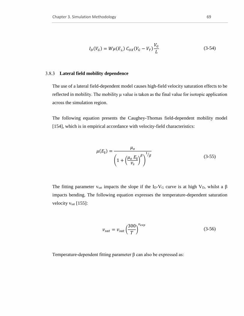
Chapter 3. Simulation Methodology 69
𝐼𝐷(𝑉𝐺) = 𝑊𝜇(𝐸⊥) 𝐶𝑂𝑋(𝑉𝐺 − 𝑉𝑇)𝑉𝐺
𝐿 (3-54)
Lateral field mobility dependence
The use of a lateral field-dependent model causes high-field velocity saturation effects to be
reflected in mobility. The mobility μ value is taken as the final value for isotopic application
across the simulation region.
The following equation presents the Caughey-Thomas field-dependent mobility model
[154], which is in empirical accordance with velocity-field characteristics:
𝜇(𝐸∥) =𝜇𝑜
(1 + (𝜇𝑜 𝐸∥
𝑣𝑠)
𝛽
)
1𝛽⁄
(3-55)
The fitting parameter vsat impacts the slope if the ID-VG curve is at high VD, whilst a β
impacts bending. The following equation expresses the temperature-dependent saturation
velocity vsat [155]:
𝑣𝑠𝑎𝑡 = 𝑣𝑠𝑎𝑡 (300
𝑇)
𝑣𝑒𝑥𝑝
(3-56)
Temperature-dependent fitting parameter β can also be expressed as:
Chapter 3. Simulation Methodology 70
𝛽 = 𝛽𝑜 (300
𝑇)
𝛽𝑒𝑥𝑝
(3-57)
The high drain bias the simple current model in the saturation region is expressed as:
𝐼𝐷(𝑉𝐺) =𝑊
2𝐿𝜇(𝐸∥) 𝐶𝑂𝑋(𝑉𝐺 − 𝑉𝑇)2 (3-58)
In the simple current model in the saturation region the lateral field can be approximated as
Ell = VD/L, with work function again used as a VT as the fitting parameter taking into account
the impact of the short channel effects.
TCAD Tools and Data Analyses
This research has adopted the GSS 3D statistical atomistic TCAD simulator GARAND and
the automation and optimisation engine Enigma, which offer significant accuracy and
efficiency in device calibration, optimisation and modelling.
3.9.1 GARAND
GARAND used comprehensively in this research is a TCAD simulator specifically
developed to simulate statistical variability and reliability in contemporary and future
CMOS transistor. The GSS (Synopsys) website details a number of applications of the
GARAND tool in this context. GARAND has offers different simulation modules, including
Monte Carlo, drift-diffusion with PS and DG quantum corrections. Additionally, GARAND
also provides the latest physical models, supporting accuracy at atomic scale. The tool
provides the ability to use density gradient quantum corrections for both electrons and holes
simultaneously. Additionally, GARAND also offers extremely efficient computation with
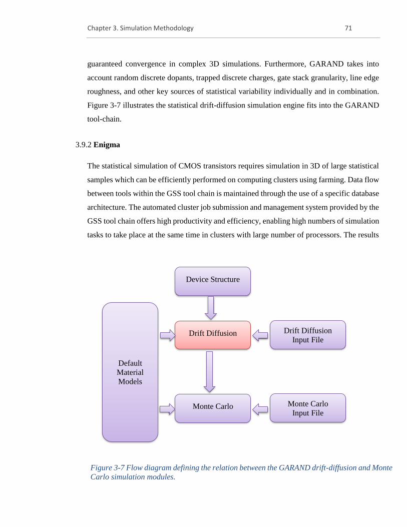
Chapter 3. Simulation Methodology 71
guaranteed convergence in complex 3D simulations. Furthermore, GARAND takes into
account random discrete dopants, trapped discrete charges, gate stack granularity, line edge
roughness, and other key sources of statistical variability individually and in combination.
Figure 3-7 illustrates the statistical drift-diffusion simulation engine fits into the GARAND
tool-chain.
3.9.2 Enigma
The statistical simulation of CMOS transistors requires simulation in 3D of large statistical
samples which can be efficiently performed on computing clusters using farming. Data flow
between tools within the GSS tool chain is maintained through the use of a specific database
architecture. The automated cluster job submission and management system provided by the
GSS tool chain offers high productivity and efficiency, enabling high numbers of simulation
tasks to take place at the same time in clusters with large number of processors. The results
Device Structure
Drift Diffusion
Monte Carlo
Default
Material
Models
Drift Diffusion
Input File
Monte Carlo
Input File
Figure 3-7 Flow diagram defining the relation between the GARAND drift-diffusion and Monte
Carlo simulation modules.
Chapter 3. Simulation Methodology 72
of the simulations are automatically gathered and summarised through the job submission
and management interface with the GSS database.
Summary
This chapter has outlined in the basis of the 3D drift/diffusion simulation, presenting both
the drift/diffusion and the density gradient equations as well as the algorithms employed
solve them self consistently. Semi-classical approaches are used to simulate the charge
transport based on the Monte Carlo method, where the charge trajectories between two
scattering events are simulated using classical dynamics. Fermi’s golden rule [156] is uses,
to calculate the scattering rates based on analytical non-parabolic band structure. The 3D
EMC simulations are used to capture the non-equilibrium transport in aggressively-scaled
NWT, leading to accurate estimation of the transistor performance. This chapter has also
described the quantum correction based on the solution to 2D Poisson-Schrodinger
equations for each discretisation cross-sectional plane perpendicular to the transport
direction [157]. The quantum potential obtained from the PS solution determines the driving
field, which controls the free flight of the particles. This chapter has also discussed the
stability and efficiency of the DD simulation method, with a straightforward yet effective
DG approach to the introduction of quantum effects into simulation. It was clarified that
non-equilibrium transport effects cannot be represented by the DD model in nano-scale
devices. Furthermore, transport variability due to ionised impurity scattering is also difficult
to capture using DD- simulation. Monte Carlo simulation are used to calibrate the drift-
diffusions of large multichannel NWTs and to perform statistical variability simulations
[158].
Chapter 4. Si Nanowire Transistors Design 73
4 Chapter 4. Si Nanowire Transistors Design
Introduction:
Electronics manufacturers, influenced by Moore’s law, have been drawn into innovating
many key technical CMOS technology developments including high-k gate dielectrics
technology and strain technology, which involve both new processes and new materials
[26], [159]–[161]. Multi-gate MOS FET modelling is anticipated to be a primary focus for
future developments. The superior electrostatic integrity provided by Nanowire (all gate
around) Transistors (NWT) [7]–[9], [162] ensures that these innovative transistors remain
popular candidates for achieving ultimate CMOS scaling limits [162]–[164]. The scaling
limits are ultimately defined by the quantum mechanical effects which control the operation
of NWT transistors [4]. Threshold voltage shift, resulting from confinement effects,
together with the reduction of the gate-to-channel capacitance are reducing the available for
transport charge within the channel [6]. Lower gate-to-channel capacitance will additionally
negatively impact the electrostatic integrity. These effects increase with the reduction of the
NWT dimensions and are therefore key to the assessment of NWT scaling limits [9].
Density gradient quantum corrections, in commercially available TCAD tools, represent the
pragmatic approach for dealing with quantum confinement effects [7]. However, no
investigations of the importance of quantum effects and the relevance of the DG technique
for the modelling of ultimately scaled NWTs of varying cross-sectional shape at the scaling
limits have yet been conducted. This means that the effect of NWT cross-sectional shape
on ultimate scaling limits remains unaddressed, along with other critical design questions.
This chapter examines the ultimate scaling limits of NWTs with different cross-sectional
shapes, using simulations employing Poisson Schrodinger (PS) quantum corrections
implemented in the ‘atomistic’ drift-diffusion (DD) simulator GARAND [GSS]. Realistic
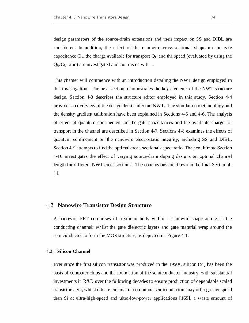
Chapter 4. Si Nanowire Transistors Design 74
design parameters of the source-drain extensions and their impact on SS and DIBL are
considered. In addition, the effect of the nanowire cross-sectional shape on the gate
capacitance CG, the charge available for transport QG and the speed (evaluated by using the
QG/CG ratio) are investigated and contrasted with τ.
This chapter will commence with an introduction detailing the NWT design employed in
this investigation. The next section, demonstrates the key elements of the NWT structure
design. Section 4-3 describes the structure editor employed in this study. Section 4-4
provides an overview of the design details of 5 nm NWT. The simulation methodology and
the density gradient calibration have been explained in Sections 4-5 and 4-6. The analysis
of effect of quantum confinement on the gate capacitances and the available charge for
transport in the channel are described in Section 4-7. Sections 4-8 examines the effects of
quantum confinement on the nanowire electrostatic integrity, including SS and DIBL.
Section 4-9 attempts to find the optimal cross-sectional aspect ratio. The penultimate Section
4-10 investigates the effect of varying source/drain doping designs on optimal channel
length for different NWT cross sections. The conclusions are drawn in the final Section 4-
11.
Nanowire Transistor Design Structure
A nanowire FET comprises of a silicon body within a nanowire shape acting as the
conducting channel; whilst the gate dielectric layers and gate material wrap around the
semiconductor to form the MOS structure, as depicted in Figure 4-1.
4.2.1 Silicon Channel
Ever since the first silicon transistor was produced in the 1950s, silicon (Si) has been the
basis of computer chips and the foundation of the semiconductor industry, with substantial
investments in R&D over the following decades to ensure production of dependable scaled
transistors. So, whilst other elemental or compound semiconductors may offer greater speed
than Si at ultra-high-speed and ultra-low-power applications [165], a waste amount of
Chapter 4. Si Nanowire Transistors Design 75
additional R&D expenditure in time and money would be required to deliver and optimise
corresponding new chip manufacturing and design processes. A primary advantage of Si is
its susceptibility to oxidation that produce silicon dioxide SiO2, a gate dielectric with
exceptional properties. The oxidation proceeds in dry or wet oxygen atmosphere at high
temperature. Si also remains stable at high temperatures of operation. Additionally, Si is
insoluble in water and this is beneficial in minimising various problems associated with
manufacturing and functionality. Si exists naturally as a perfect crystal with only minute
defects apparent in ultra-large ULSI integrated chips. Si is also inexpensive and commonly
sourced across the Earth. These properties make Si the semiconductor of preference in the
production of robust transistors and chips.
Based on a set of commercial criteria, for each technology node, a key research objective
is to continually investigate a variety of transistor scenarios with the aim of ensuring that Si
remains the basis for future chip manufacturing. Strained Si has demonstrated important
key benefits for improving transistor performance, particularly with regard to p-type
MOSFETs. Particular strain patterns result in tripling the hole mobility and doubling the on-
state current of p-type transistors. Further to Si strain development, alternative channel
materials are also being investigated for their potential of enhancing MOSFETs speed.
Figure 4-1 schematic view and material details of the circular NWT (S/D contacts
are not shown).
Chapter 4. Si Nanowire Transistors Design 76
4.2.2 Gate dielectrics layers
Excessive scaling of SiO2 layer results in higher gate leakage as a consequence of quantum
mechanical tunneling effects [166]. Minimising the gate leakage current in CMOS
components, necessitates replacing the traditional SiO2 gate dielectric layer with an
alternative dielectric of higher dielectric constant ‘high-k’. HFO2 has high permittivity (k
> 20) and has therefore was introduced as an alternative gate dielectric.
Conversely, Hafnia and the majority of high-k MOS dielectrics have unstable interfaces with
Si channels. Here the high-k layer reacts with Si under equilibrium conditions to produce an
undesired interfacial layer (IL). To enhance the capacitance of the gate stack and match the
high-k layer with the Si interface, an insulating interfacial layer is needed [167]. The
insulating interface provided by SiO2 circumvents undesired movements of threshold
voltage and flat band voltage. It also offers improved thermodynamic stability [168].
Insertion of a thin IL of SiO2 between the high-k gate stacks and Si channel promotes
reliability by lowering ITC (interface trap density) defects at the Si-interface [29], [166],
[167], [169]–[174]. The IL lowers gate stacked/Si roughness and improves the mobility
[175]. The peak mobility in MOSFET devices with a high-k layer has been shown to be
dependent not only on IL material, but also to be directly proportional to IL thickness for
both poly-Si and metal gates [176], [177].
Conversely, the hafnia thickness tends to increase the low-frequency noise associated with
the MOSFET current when compared with SiO2 alternatives. The IL minimises noise, whilst
reducing SiO2 thickness results in greater, low-frequency noise as a consequence of interface
trapping and mobility variations [178], [179].
The SiO2 IL is found between the Si conducting channel and the high-κ dielectric layer can
be deliberate or unintentional. The thin IL develops between the high-κ layer and the Si as
a consequence of many high-κ dielectric deposition techniques resulting in thermally
unstable interfaces with Si. The IL derives from the diffusion of oxygen from the high-κ
layer towards the Si interface mainly during the process of activation annealing, rather than
the process of high-κ deposition itself. The molecular bonding of Si atoms to oxygen
Chapter 4. Si Nanowire Transistors Design 77
promotes the controlled diffusion of the oxygen by producing high-κ stacks with SiO2
IL[180], [181].
Whilst the IL offers improved mobility, better stability and reduced noise for high-k gate
stacks, it also lowers the total gate capacitance [174], [182], [183]. The total capacitance of
MOS devices comprises the two dielectrics layers in series (4-1):
1
𝐶𝑜𝑥=
1
𝐶𝑆𝑖𝑂2
+1
𝐶ℎ𝑖𝑔ℎ−𝑘
(4-1)
The MOS capacitance Cox is determined by dielectric primitivity and thickness as described
in equation (4-2):
𝐶𝑜𝑥 =휀𝑜𝑥휀𝑜
𝑡𝑜𝑥 (4-2)
Where Ɛox represents the relative dielectric permittivity, Ɛo represents the permittivity of
vacuum, and tox represents the oxide thickness. More specifically, the employing a dielectric
with high Ɛox more facilitates the scaling to the transistor dimensions. The expression
“equivalent oxide thickness” (EOT) is employed to extrapolate the thickness of SiO2
necessary to achieve capacitance of high-k material of an equivalent area. The EOT equation
(4-3) is:
𝐸𝑂𝑇 = 휀𝑆𝑖𝑂2
𝑡ℎ𝑖𝑔ℎ−𝑘
휀ℎ𝑖𝑔ℎ−𝑘
(4-3)
Equations (4-1), (4-2) , and (4-3) give rise to the EOT of two layers of gate stack (4-4;
𝐸𝑂𝑇 = 휀𝑆𝑖𝑜2
(𝑡𝑆𝑖𝑂2
휀𝑆𝑖𝑜2
+𝑡ℎ𝑖𝑔ℎ−𝑘
휀ℎ𝑖𝑔ℎ−𝑘)
(4-4)
Chapter 4. Si Nanowire Transistors Design 78
4.2.3 Gate Electrodes
Metal gates, in combination with Si and appropriate dielectric, can act as gate electrodes to
form a MOS channel region. However, use of poly-Si as a gate electrode can result in
problems with poly-depletion and resistivity effects. Therefore, metallic TiN gates are used
in contemporary CMOS technologies [172].
3-D Structure Modelling Tools
Adaptable techniques are required for modelling the new innovative 3-D Nano-transistors.
This study uses the Structure Editor Sigmund [GSS] to generate accurate simulation domains
of nanowire structures stored in VTK format which can be loaded and used by the device
simulator GARAND. The hierarchy of object structure flow employed by the Sigmund
Structure Editor is depicted in Figure 4-2. The structure editor sets the 3-D simulation
domain, which can then be populated with material regions, doping regions and contact.
Sigmund also meshes the simulation domain prior storing it in the VTK file. This is a five-
step process:
1- Identification of materials, doping type, dimensions and other device parameters.
2- Utilisation of the template geometry objects (triangular prism, cylinder, cuboid,
tetrahedron, regular tetrahedron and sphere) to generate the 3-D structure.
Amalgamations of the template objects permits creation of more complex structures.
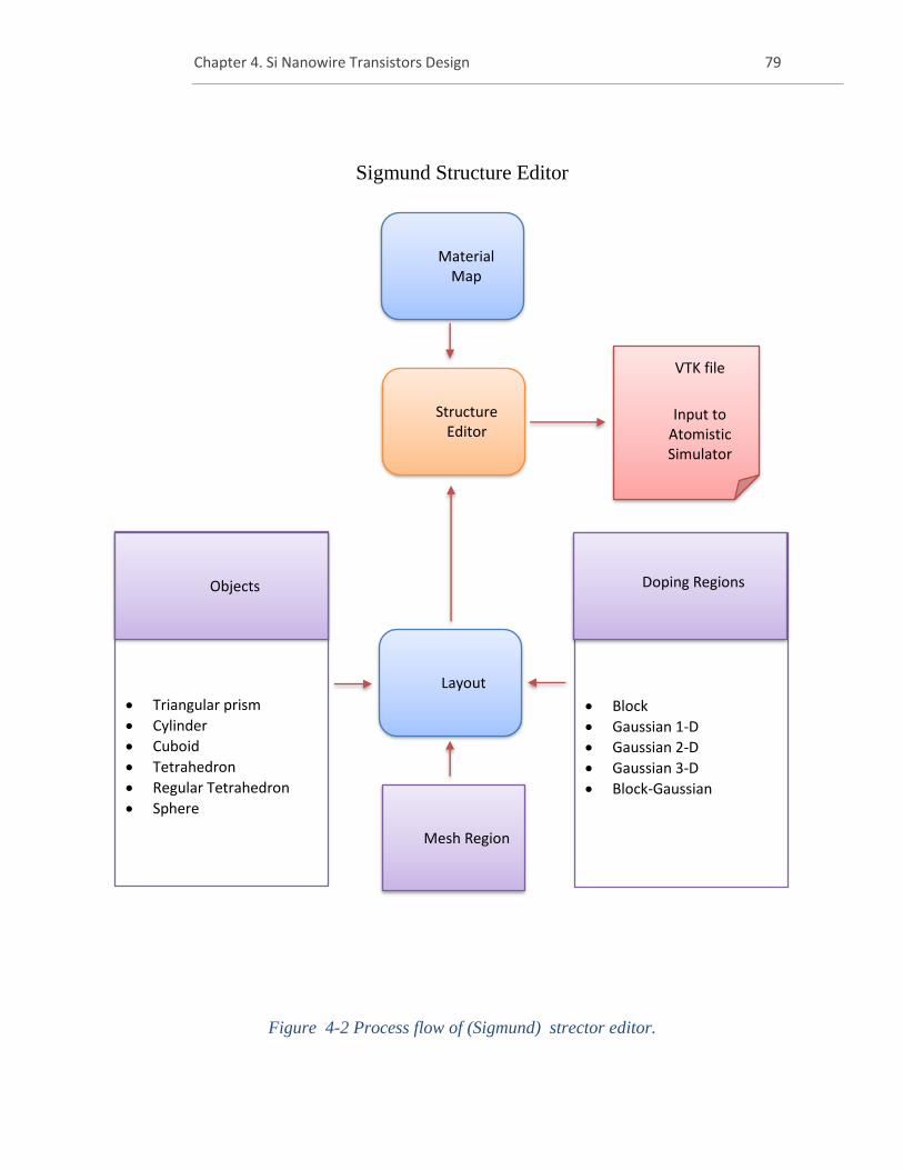
Chapter 4. Si Nanowire Transistors Design 79
Sigmund Structure Editor
Layout
Structure Editor
Material Map
• Block
• Gaussian 1-D
• Gaussian 2-D
• Gaussian 3-D
• Block-Gaussian
Doping Regions
• Triangular prism
• Cylinder
• Cuboid
• Tetrahedron
• Regular Tetrahedron
• Sphere
Objects
Mesh Region
VTK file
Input to Atomistic Simulator
Figure 4-2 Process flow of (Sigmund) strector editor.
Chapter 4. Si Nanowire Transistors Design 80
3- Following the generation of the structure, doping can be introduced via inbuilt analytical
doping regions employing a combination of position and materials options. The
Sigmund Structure Editor offers five doping options: Block, Gaussian 1-D, Gaussian 2-
D, Gaussian 3-D, Block-Gaussian.
4- Whilst meshing is defined at the same time as the objects, remeshing can be applied at
any time to achieve target resolution.
5- Metal gate granularity and line edge roughness (LER) are additional options which can
be used to supplement the device structure or selected objects.
5 mm Nanowire Transistor Design
Key design criteria:
1- Material composition of channel, interfacial layer, high-k gate stack.
2- Dimensions of device cross-sectional shape, gate length, effective oxide thickness and
source/drain spacers.
3- Crystallographic orientations and strain of the semiconductor channel.
4- Doping concentrations, such as peak and roll-off doping.
Si is used for the simulated NWT channel, source, and drain regions. SiO2 and Hafnia
comprise the 0.4 nm interfacial layer and 0.8 nm high-k layer determine the gate stack
(according to the ITRS scaling criteria). According to Equation 4-4 this results in gives
equivalent effective oxide thickness EOT=0.6. Figure 4-3 depicts the 3D structure of a
cylinder NWT. In this investigation, the electrostatic performance is examined for silicon
channels with four different cross-sectional shapes: circle; ellipse; rectangular; square. To
ensure an unbiased comparison, all cross-sectional shapes were designed with identical
Chapter 4. Si Nanowire Transistors Design 81
surface areas: Across-section= 9π nm2, i.e. the diameter or (fin-pitch) of the circular NWT is
6nm. Table 4-1 gives the precise cross-sectional dimensions for all four investigated shapes.
The two channel crystallographic orientations studied on (001) wafer are <110> and <100>.
Table 4-2 summarises design parameters for all devices: the effective gate length is 10-20
nm, the spacer thickness is 5nm, the source/drain peak doping concentration is 4x1020 cm-3
The low channel doping boosts charge mobility with a significant improvement of the FET
performance and it also reduce local (statistical) variability. It has been demonstrated that
doped FinFETs retain a variability advantage over classical planar MOSFET if the channel
doping is lower than a few 1018cm-3 [184]. The channel doping of Intel 14nm FinFET is
about 1017 cm-3. Better electrostatic integrity, offered by gate-all-around nanowire transistor
(NWT) architectures allow reducing the doping of the channel [7]. [8], [9], [162], [164],
[185]–[189]. In this study, the channel doping is lowered up to 1014 cm-3.
Sigmund Structure Editor was used to generate suitable NWT structures for this study.
Figure 4-4 depicts the doping profile of the Si NWT studied with a gate length Lg = 12 nm
and spacer length Ls = 5 nm.
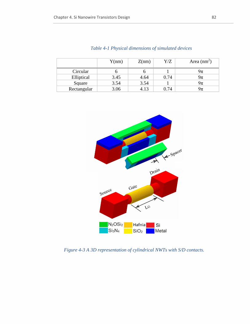
Chapter 4. Si Nanowire Transistors Design 82
Figure 4-3 A 3D representation of cylindrical NWTs with S/D contacts.
Table 4-1 Physical dimensions of simulated devices
Y(nm) Z(nm) Y/Z Area (nm2)
Circular 6 6 1 9π
Elliptical 3.45 4.64 0.74 9π
Square 3.54 3.54 1 9π
Rectangular 3.06 4.13 0.74 9π
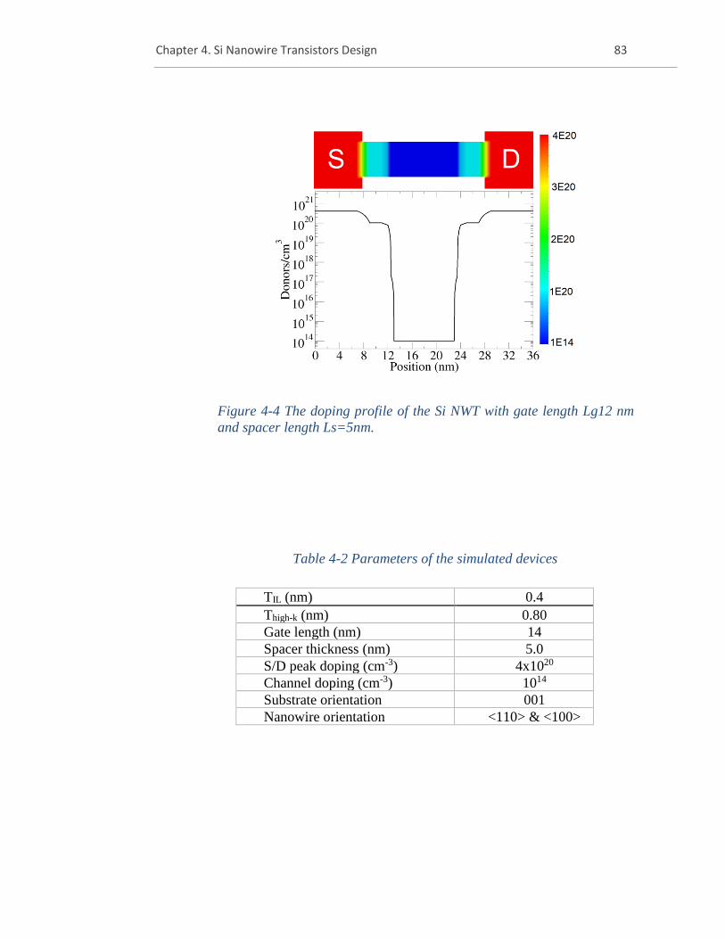
Chapter 4. Si Nanowire Transistors Design 83
Figure 4-4 The doping profile of the Si NWT with gate length Lg12 nm
and spacer length Ls=5nm.
Table 4-2 Parameters of the simulated devices
TIL (nm) 0.4
Thigh-k (nm) 0.80
Gate length (nm) 14
Spacer thickness (nm) 5.0
S/D peak doping (cm-3) 4x10²⁰
Channel doping (cm-3) 1014
Substrate orientation 001
Nanowire orientation <110> & <100>
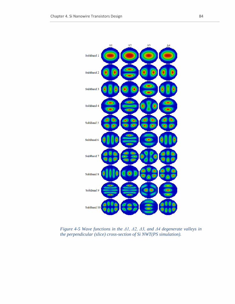
Chapter 4. Si Nanowire Transistors Design 84
Figure 4-5 Wave functions in the Δ1, Δ2, Δ3, and Δ4 degenerate valleys in
the perpendicular (slice) cross-section of Si NWT(PS simulation).
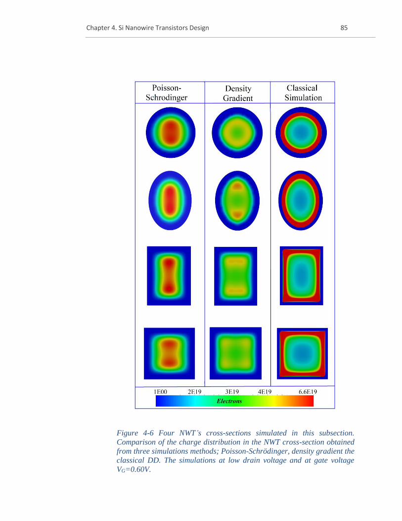
Chapter 4. Si Nanowire Transistors Design 85
Figure 4-6 Four NWT’s cross-sections simulated in this subsection.
Comparison of the charge distribution in the NWT cross-section obtained
from three simulations methods; Poisson-Schrödinger, density gradient the
classical DD. The simulations at low drain voltage and at gate voltage
VG=0.60V.
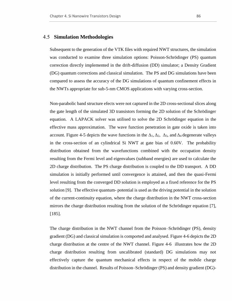
Chapter 4. Si Nanowire Transistors Design 86
Simulation Methodologies
Subsequent to the generation of the VTK files with required NWT structures, the simulation
was conducted to examine three simulation options: Poisson-Schrödinger (PS) quantum
correction directly implemented in the drift-diffusion (DD) simulator; a Density Gradient
(DG) quantum corrections and classical simulation. The PS and DG simulations have been
compared to assess the accuracy of the DG simulations of quantum confinement effects in
the NWTs appropriate for sub-5-nm CMOS applications with varying cross-section.
Non-parabolic band structure efects were not captured in the 2D cross-sectional slices along
the gate length of the simulated 3D transistors forming the 2D solution of the Schrödinger
equation. A LAPACK solver was utilised to solve the 2D Schrödinger equation in the
effective mass approximation. The wave function penetration in gate oxide is taken into
account. Figure 4-5 depicts the wave functions in the Δ1, Δ2, Δ3, and Δ4 degenerate valleys
in the cross-section of an cylindrical Si NWT at gate bias of 0.60V. The probability
distribution obtained from the wavefunctions combined with the occupation density
resulting from the Fermi level and eigenvalues (subband energies) are used to calculate the
2D charge distribution. The PS charge distribution is coupled to the DD transport. A DD
simulation is initially performed until convergence is attained, and then the quasi-Fermi
level resulting from the converged DD solution is employed as a fixed reference for the PS
solution [9]. The effective quantum- potential is used as the driving potential in the solution
of the current-continuity equation, where the charge distribution in the NWT cross-section
mirrors the charge distribution resulting from the solution of the Schrödinger equation [7],
[185].
The charge distribution in the NWT channel from the Poisson–Schrödinger (PS), density
gradient (DG) and classical simulation is comported and analysed. Figure 4-6 depicts the 2D
charge distribution at the centre of the NWT channel. Figure 4-6 illustrates how the 2D
charge distribution resulting from uncalibrated (standard) DG simulations may not
effectively capture the quantum mechanical effects in respect of the mobile charge
distribution in the channel. Results of Poisson–Schrödinger (PS) and density gradient (DG)-
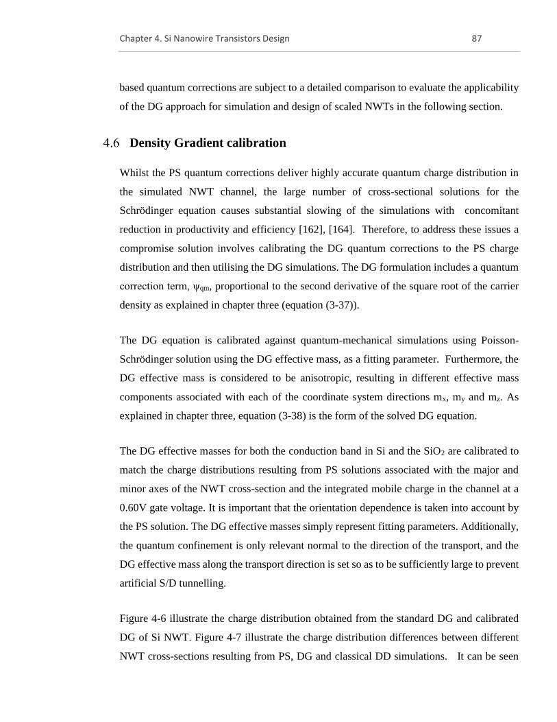
Chapter 4. Si Nanowire Transistors Design 87
based quantum corrections are subject to a detailed comparison to evaluate the applicability
of the DG approach for simulation and design of scaled NWTs in the following section.
Density Gradient calibration
Whilst the PS quantum corrections deliver highly accurate quantum charge distribution in
the simulated NWT channel, the large number of cross-sectional solutions for the
Schrödinger equation causes substantial slowing of the simulations with concomitant
reduction in productivity and efficiency [162], [164]. Therefore, to address these issues a
compromise solution involves calibrating the DG quantum corrections to the PS charge
distribution and then utilising the DG simulations. The DG formulation includes a quantum
correction term, ψqm, proportional to the second derivative of the square root of the carrier
density as explained in chapter three (equation (3-37)).
The DG equation is calibrated against quantum-mechanical simulations using Poisson-
Schrödinger solution using the DG effective mass, as a fitting parameter. Furthermore, the
DG effective mass is considered to be anisotropic, resulting in different effective mass
components associated with each of the coordinate system directions mx, my and mz. As
explained in chapter three, equation (3-38) is the form of the solved DG equation.
The DG effective masses for both the conduction band in Si and the SiO2 are calibrated to
match the charge distributions resulting from PS solutions associated with the major and
minor axes of the NWT cross-section and the integrated mobile charge in the channel at a
0.60V gate voltage. It is important that the orientation dependence is taken into account by
the PS solution. The DG effective masses simply represent fitting parameters. Additionally,
the quantum confinement is only relevant normal to the direction of the transport, and the
DG effective mass along the transport direction is set so as to be sufficiently large to prevent
artificial S/D tunnelling.
Figure 4-6 illustrate the charge distribution obtained from the standard DG and calibrated
DG of Si NWT. Figure 4-7 illustrate the charge distribution differences between different
NWT cross-sections resulting from PS, DG and classical DD simulations. It can be seen
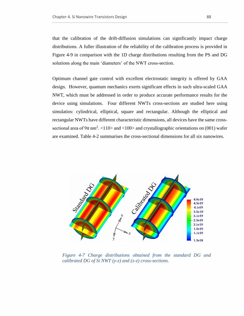
Chapter 4. Si Nanowire Transistors Design 88
that the calibration of the drift-diffusion simulations can significantly impact charge
distributions. A fuller illustration of the reliability of the calibration process is provided in
Figure 4-9 in comparison with the 1D charge distributions resulting from the PS and DG
solutions along the main ‘diameters’ of the NWT cross-section.
Optimum channel gate control with excellent electrostatic integrity is offered by GAA
design. However, quantum mechanics exerts significant effects in such ultra-scaled GAA
NWT, which must be addressed in order to produce accurate performance results for the
device using simulations. Four different NWTs cross-sections are studied here using
simulatios: cylindrical, elliptical, square and rectangular. Although the elliptical and
rectangular NWTs have different characteristic dimensions, all devices have the same cross-
sectional area of 9π nm2. <110> and <100> and crystallographic orientations on (001) wafer
are examined. Table 4-2 summarises the cross-sectional dimensions for all six nanowires.
Figure 4-7 Charge distributions obtained from the standard DG and
calibrated DG of Si NWT (y-z) and (x-z) cross-sections.
Chapter 4. Si Nanowire Transistors Design 89
Figure 4-9 1D charge distributions obtained from the PS simulation and DG
simulation. The cutline is along of perpendicular ‘diameters’ (y and z) of the
NWT’s slice at the mid of the gate.
Figure 4-8 Capacitance-voltage (C-V) characteristics of the simulated NWT with six
different cross-sections.
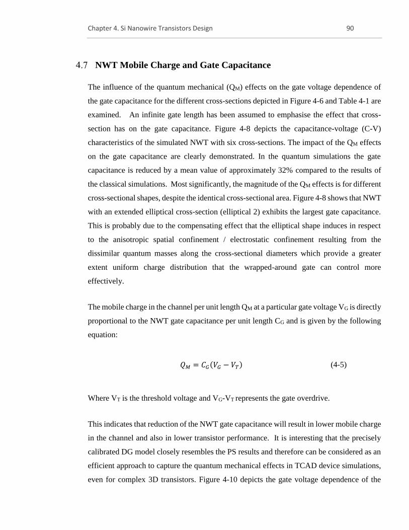
Chapter 4. Si Nanowire Transistors Design 90
NWT Mobile Charge and Gate Capacitance
The influence of the quantum mechanical (QM) effects on the gate voltage dependence of
the gate capacitance for the different cross-sections depicted in Figure 4-6 and Table 4-1 are
examined. An infinite gate length has been assumed to emphasise the effect that cross-
section has on the gate capacitance. Figure 4-8 depicts the capacitance-voltage (C-V)
characteristics of the simulated NWT with six cross-sections. The impact of the QM effects
on the gate capacitance are clearly demonstrated. In the quantum simulations the gate
capacitance is reduced by a mean value of approximately 32% compared to the results of
the classical simulations. Most significantly, the magnitude of the QM effects is for different
cross-sectional shapes, despite the identical cross-sectional area. Figure 4-8 shows that NWT
with an extended elliptical cross-section (elliptical 2) exhibits the largest gate capacitance.
This is probably due to the compensating effect that the elliptical shape induces in respect
to the anisotropic spatial confinement / electrostatic confinement resulting from the
dissimilar quantum masses along the cross-sectional diameters which provide a greater
extent uniform charge distribution that the wrapped-around gate can control more
effectively.
The mobile charge in the channel per unit length QM at a particular gate voltage VG is directly
proportional to the NWT gate capacitance per unit length CG and is given by the following
equation:
𝑄𝑀 = 𝐶𝐺(𝑉𝐺 − 𝑉𝑇) (4-5)
Where VT is the threshold voltage and VG-VT represents the gate overdrive.
This indicates that reduction of the NWT gate capacitance will result in lower mobile charge
in the channel and also in lower transistor performance. It is interesting that the precisely
calibrated DG model closely resembles the PS results and therefore can be considered as an
efficient approach to capture the quantum mechanical effects in TCAD device simulations,
even for complex 3D transistors. Figure 4-10 depicts the gate voltage dependence of the
Chapter 4. Si Nanowire Transistors Design 91
mobile charge in the channel for the NWTs in Table 4-1 (NB this refers to the integral mobile
charge in the channel per unit area at low drain bias).
Eqn. (4-5) indicates that the reduction in gate capacitance results in a reduction of mobile
charge in the channel, which consequently is an indicator of poorer NWT performance.
Similar to gate capacitance, the mobile charge for NWTs with identical cross-sectional areas
depends on the cross-sectional shape. The effects of NWT shape on potential NWT
performance can be evaluated from Table 4-3 which compares QM(VG=0.60V) for identical
QM(VG=0.0V). To perform this comparison the QM(VG) curves were aligned by changing
the gate work function. Like the gate capacitance, the elliptical 2 NWT exhibits the largest
mobile charge in the channel. Table 4-4 includes an additional case compared with the
NWTs outlined in Table 4-1: the structures in this case have been rotated by 90 degrees
whilst retaining the original crystal orientation. This perpendicular rotation of the optimal
performing NWT leads to an improved QM, CG which represents around 11% and 10%
improvement of QM/CG ratio. Here, the asymmetric spatial confinement induced by the
elliptical shape aggravates the similar electrostatic confinement induced by the various
quantum masses along the cross-section diameters, which gives rise to a charged distribution
that is predominantly focussed on only one of the two diameters and consequently less
tightly controlled by the wrapped-around gate. Table 4-3 illustrates how the QM/CG ratio can
be utilised as an indicator for the ‘intrinsic’ NWT speed. QM and QM/CG are directly
correlated which highlights not only the approximate nature of Eqn (4-5), but also the
requirement to assess both QM and CG. Extended elliptical NWT exhibits the optimum
QM/CG when compared to the other cross-sections. Table 4-5 provides the values for QM, CG
and QM/CG ratio for the wires with identical matching cross-sectional areas as presented in
Table 4-3, but also including the <100> channel orientation. Analyzing the results
summarized in Table 4-3, Table 4-4, Table 4-5, gives rise to the following main conclusions.
First, all wires with the <100> channel direction have greater charge in the channel
compared to the <110> wires. This confirms that varying the crystal orientation of the silicon
channel results in change of mobile charge within the channel and therefore is an important
design parameter. Consequently, the gate capacitance also increases leading to enhanced
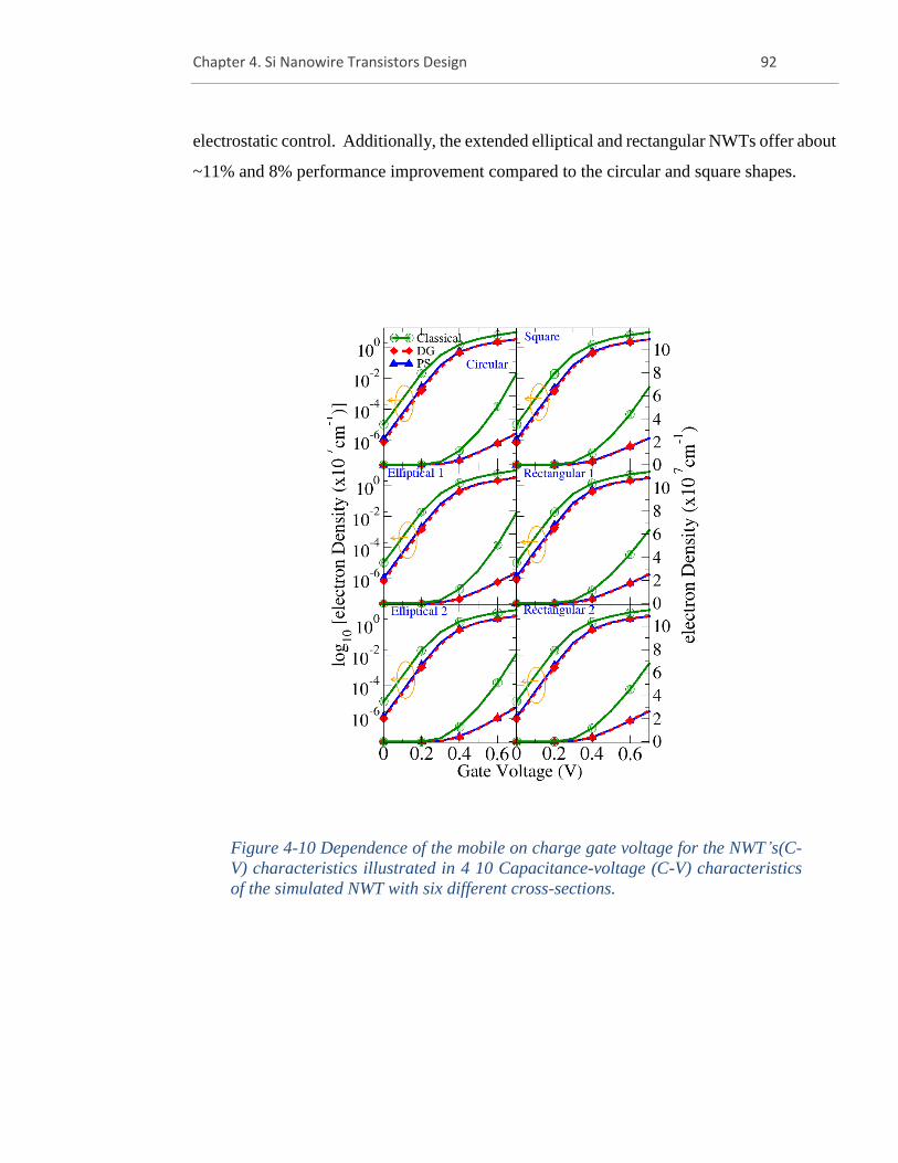
Chapter 4. Si Nanowire Transistors Design 92
electrostatic control. Additionally, the extended elliptical and rectangular NWTs offer about
~11% and 8% performance improvement compared to the circular and square shapes.
Figure 4-10 Dependence of the mobile on charge gate voltage for the NWT’s(C-
V) characteristics illustrated in 4 10 Capacitance-voltage (C-V) characteristics
of the simulated NWT with six different cross-sections.
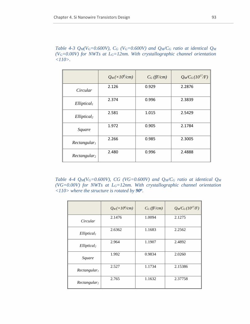
Chapter 4. Si Nanowire Transistors Design 93
Table 4-3 QM(VG=0.600V), CG (VG=0.600V) and QM/CG ratio at identical QM
(VG=0.00V) for NWTs at LG=12nm. With crystallographic channel orientation
<110>.
QM (×106/cm) CG (fF/cm) QM/CG (1017/F)
Circular 2.126 0.929 2.2876
Elliptical1 2.374 0.996 2.3839
Elliptical2 2.581 1.015 2.5429
Square 1.972 0.905 2.1784
Rectangular1 2.266 0.985 2.3005
Rectangular2 2.480 0.996 2.4888
Table 4-4 QM(VG=0.600V), CG (VG=0.600V) and QM/CG ratio at identical QM
(VG=0.00V) for NWTs at LG=12nm. With crystallographic channel orientation
<110> where the structure is rotated by 90o.
QM (×106/cm) CG (fF/cm) QM/CG (1017/F)
Circular 2.1476 1.0094 2.1275
Elliptical1 2.6362 1.1683 2.2562
Elliptical2 2.964 1.1907 2.4892
Square 1.992 0.9834 2.0260
Rectangular1 2.527 1.1734 2.15386
Rectangular2 2.765 1.1632 2.37758
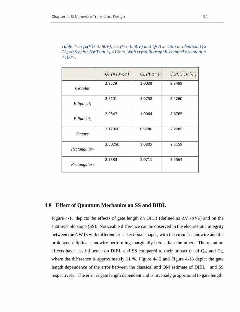
Chapter 4. Si Nanowire Transistors Design 94
Effect of Quantum Mechanics on SS and DIBL
Figure 4-11 depicts the effects of gate length on DILB (defined as ΔVT/ΔVD) and on the
subthreshold slope (SS). Noticeable difference can be observed in the electrostatic integrity
between the NWTs with different cross-sectional shapes, with the circular nanowire and the
prolonged elliptical nanowire performing marginally better than the others. The quantum
effects have less influence on DIBL and SS compared to their impact on of QM and CG,
where the difference is approximately 11 %. Figure 4-12 and Figure 4-13 depict the gate
length dependence of the error between the classical and QM estimate of DIBL and SS
respectively. The error is gate length dependent and is inversely proportional to gate length.
Table 4-5 QM(VG=0.60V), CG (VG=0.60V) and QM/CG ratio at identical QM
(VG=0.0V) for NWTs at LG=12nm. With crystallographic channel orientation
<100>.
QM (×106/cm) CG (fF/cm) QM/CG (1017/F)
Circular
2.3579 1.0038 2.3489
Elliptical1 2.6101 1.0758 2.4260
Elliptical2 2.9347 1.0964 2.6765
Square 2.17960 0.9780 2.2285
Rectangular1 2.50250 1.0805 2.3159
Rectangular2
2.7383 1.0711 2.5564
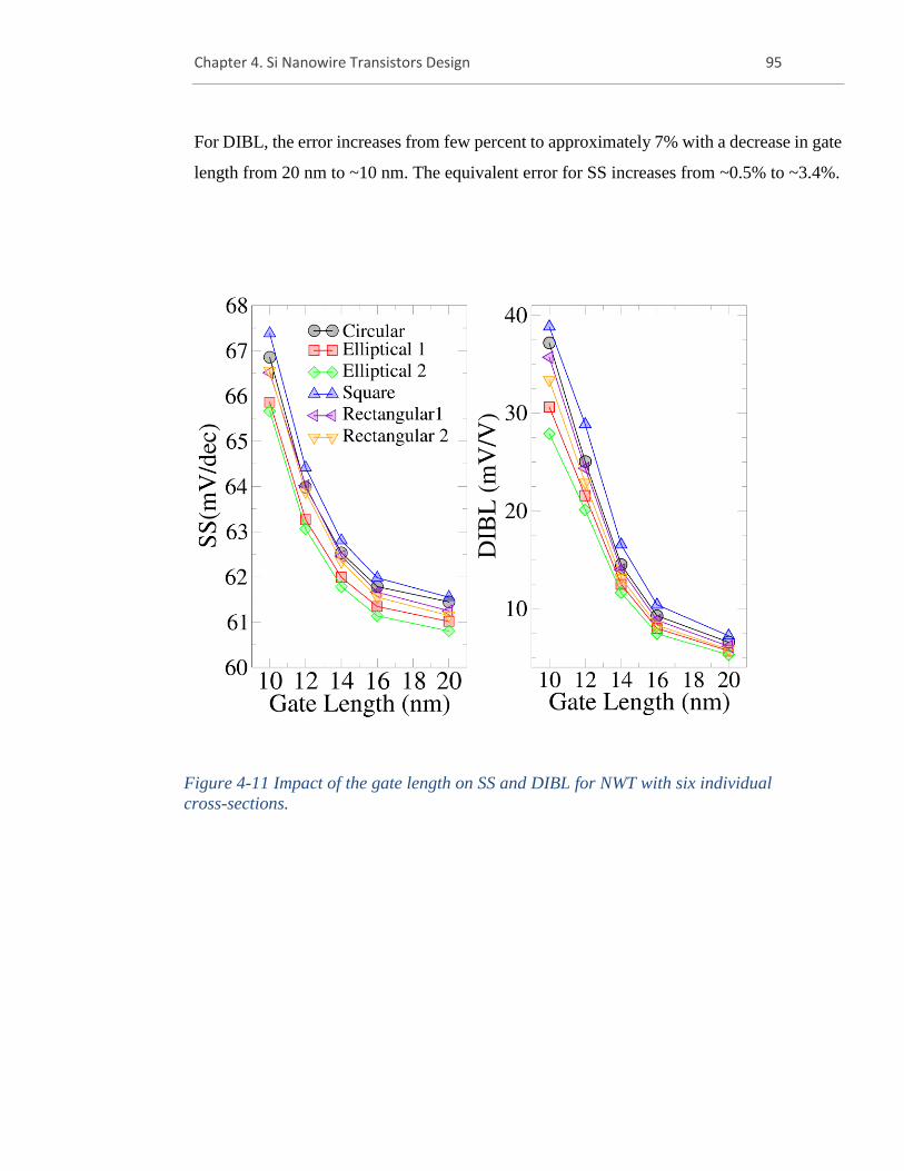
Chapter 4. Si Nanowire Transistors Design 95
For DIBL, the error increases from few percent to approximately 7% with a decrease in gate
length from 20 nm to ~10 nm. The equivalent error for SS increases from ~0.5% to ~3.4%.
Figure 4-11 Impact of the gate length on SS and DIBL for NWT with six individual
cross-sections.
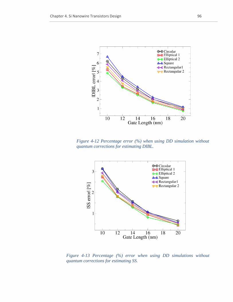
Chapter 4. Si Nanowire Transistors Design 96
Figure 4-13 Percentage (%) error when using DD simulations without
quantum corrections for estimating SS.
Figure 4-12 Percentage error (%) when using DD simulation without
quantum corrections for estimating DIBL.
Chapter 4. Si Nanowire Transistors Design 97
Optimum Cross-Sectional Aspect Ratio
It has been clearly demonstrated that the cross-sectional shape of NWT’s gate has strong
impact on gate capacitance CG and mobile charge QM in the NWTs. It has been
demonstrated that the NWT with <110> channel orientation and elongated elliptical cross-
section where the long diameter is parallel to the Si wafer surface exhibits the highest mobile
charge for any given gate voltage. The major to minor axis ratios (cross-section aspect ratio
[AR]) have been highlighted as a important design parameter determining the device
performance. Nonetheless, experimentally NWTs are still typically produced in two
versions: circular (or elliptical) NWT and nanosheet (or nanoslab) FET. Each version comes
with its own advantages and disadvantages. The fundamental difference between these two
versions remains the cross-sectional AR. However, critical design questions addressing the
optimal NWT cross-sectional aspect ratio, remain unanswered.
In an attempt to remedy this situation, the effect of varying the AR of GAA NWT while
keeping a constant cross-sectional area has been investigated. An interesting finding
emerged from this investigation was that the observed signatures of isotropic/anisotropic
charge distributions exhibit the same attributes as the golden ratio (Phi).
The structure, and dimensional characteristics associated with NWTs suitable for 5 nm Si
CMOS technology will be investigated, along with the ratio of quantum mobile charge to
gate capacitance, using the intrinsic delay (τ) as a marker for the intrinsic speed and NWT
performance. Quantum confinement effects are also considered to ensure the acuracy of the
simulations.
The NWT structure comprises a single lateral NWT. To evaluate optimal AR, the NWT
structure illustrated in Figure 4-3 is utilised. Here the Si channel is wrapped by a 0.4 nm
SiO2 IL and a 0.8 nm HFO2 (High-k) layer in the gate region. The channel doping level is 1
x 1014/cm3, rising to 1 x 10²⁰/cm3 in the extensions, and to 4 x 10²⁰/cm3 in the source/drain
regions. The x-axis is used for charge transport direction alignment. Table 4-6 outlines the
cross-sectional dimensions for 9 elongated elliptical shape nanowires with matching cross-
sectional areas of 10π nm2. The NWT y-axis diameter ranges between 4.440 nm to 9.0 nm,
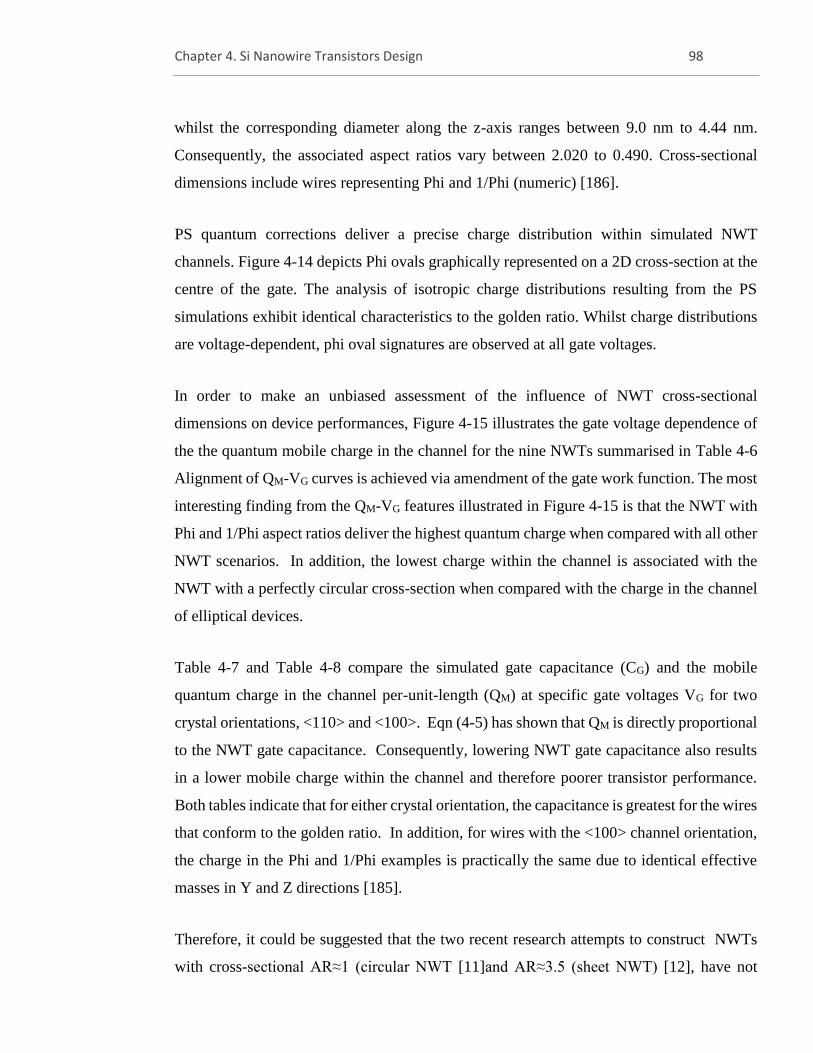
Chapter 4. Si Nanowire Transistors Design 98
whilst the corresponding diameter along the z-axis ranges between 9.0 nm to 4.44 nm.
Consequently, the associated aspect ratios vary between 2.020 to 0.490. Cross-sectional
dimensions include wires representing Phi and 1/Phi (numeric) [186].
PS quantum corrections deliver a precise charge distribution within simulated NWT
channels. Figure 4-14 depicts Phi ovals graphically represented on a 2D cross-section at the
centre of the gate. The analysis of isotropic charge distributions resulting from the PS
simulations exhibit identical characteristics to the golden ratio. Whilst charge distributions
are voltage-dependent, phi oval signatures are observed at all gate voltages.
In order to make an unbiased assessment of the influence of NWT cross-sectional
dimensions on device performances, Figure 4-15 illustrates the gate voltage dependence of
the the quantum mobile charge in the channel for the nine NWTs summarised in Table 4-6
Alignment of QM-VG curves is achieved via amendment of the gate work function. The most
interesting finding from the QM-VG features illustrated in Figure 4-15 is that the NWT with
Phi and 1/Phi aspect ratios deliver the highest quantum charge when compared with all other
NWT scenarios. In addition, the lowest charge within the channel is associated with the
NWT with a perfectly circular cross-section when compared with the charge in the channel
of elliptical devices.
Table 4-7 and Table 4-8 compare the simulated gate capacitance (CG) and the mobile
quantum charge in the channel per-unit-length (QM) at specific gate voltages VG for two
crystal orientations, <110> and <100>. Eqn (4-5) has shown that QM is directly proportional
to the NWT gate capacitance. Consequently, lowering NWT gate capacitance also results
in a lower mobile charge within the channel and therefore poorer transistor performance.
Both tables indicate that for either crystal orientation, the capacitance is greatest for the wires
that conform to the golden ratio. In addition, for wires with the <100> channel orientation,
the charge in the Phi and 1/Phi examples is practically the same due to identical effective
masses in Y and Z directions [185].
Therefore, it could be suggested that the two recent research attempts to construct NWTs
with cross-sectional AR≈1 (circular NWT [11]and AR≈3.5 (sheet NWT) [12], have not
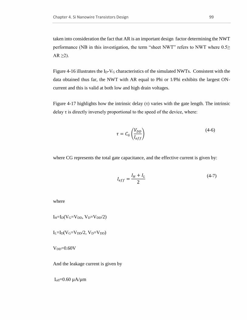
Chapter 4. Si Nanowire Transistors Design 99
taken into consideration the fact that AR is an important design factor determining the NWT
performance (NB in this investigation, the term “sheet NWT” refers to NWT where 0.5≥
AR ≥2).
Figure 4-16 illustrates the ID-VG characteristics of the simulated NWTs. Consistent with the
data obtained thus far, the NWT with AR equal to Phi or 1/Phi exhibits the largest ON-
current and this is valid at both low and high drain voltages.
Figure 4-17 highlights how the intrinsic delay (τ) varies with the gate length. The intrinsic
delay τ is directly inversely proportional to the speed of the device, where:
𝜏 = 𝐶𝐺 (
𝑉𝐷𝐷
𝐼𝑒𝑓𝑓)
(4-6)
where CG represents the total gate capacitance, and the effective current is given by:
𝐼𝑒𝑓𝑓 =
𝐼𝐻 + 𝐼𝐿
2
(4-7)
where
IH=ID(VG=VDD, VD=VDD/2)
IL=ID(VG=VDD/2, VD=VDD)
VDD=0.60V
And the leakage current is given by
Ioff=0.60 µA/µm
Chapter 4. Si Nanowire Transistors Design 100
Figure 4-17 shows that the NTWs with dimensions 8.1nm x 5nm and 5nm x 8.1nm have the
shortest intrinsic delay. The assessment of the intrinsic delay corroborates the results of
QM/CG summarised in Table 4-7.
Table 4-6 Physical dimensions of the cross-section of simulated NWTs
Z(nm)x Y(nm) Y/Z Area (nm2)
4.44×9.0 2.0200 10.0π
5.0×8.1 (Phi) 1.6200 10.0π
5.7×7.0 0.8100 10.0π
6.0×6.66 0.900 10.0π
6.32×6.32 1.00 10.0π
6.66×6.0 1.110 10.0π
7.0×5.7 1.220 10.0π
8.1×5.0 (1/ Phi) 0.620 10.0π
9.0×4.44 0.490 10.0π
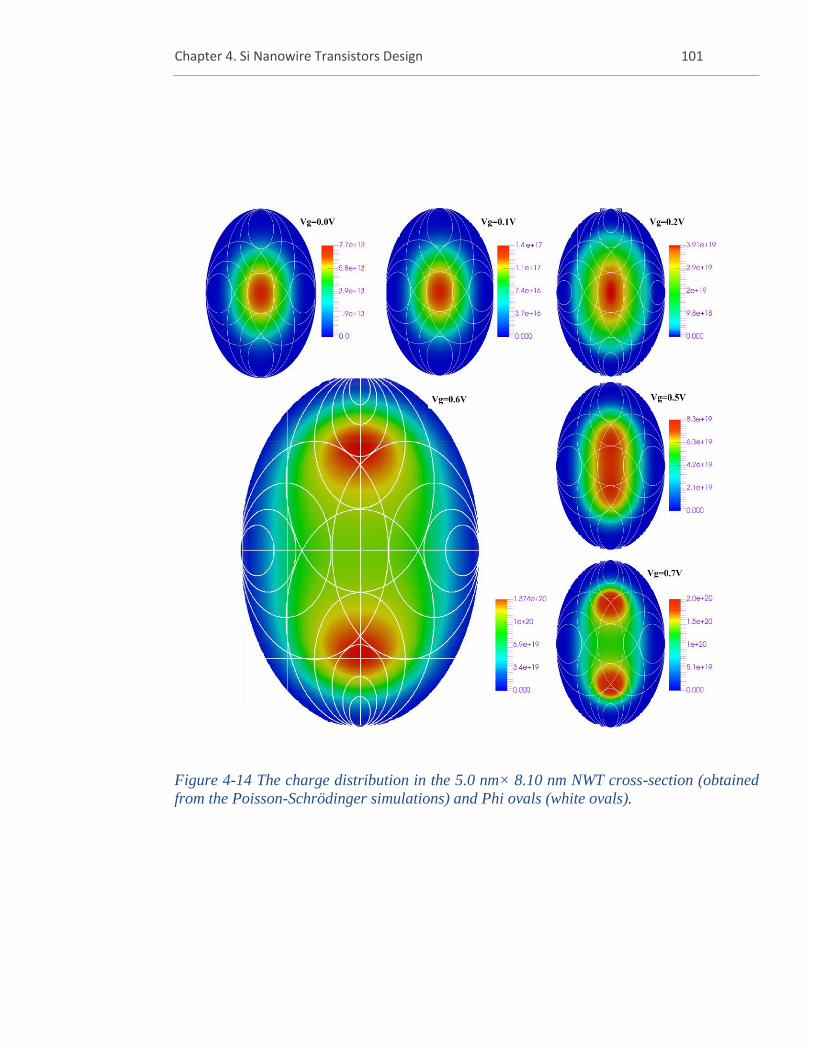
Chapter 4. Si Nanowire Transistors Design 101
Figure 4-14 The charge distribution in the 5.0 nm× 8.10 nm NWT cross-section (obtained
from the Poisson-Schrödinger simulations) and Phi ovals (white ovals).
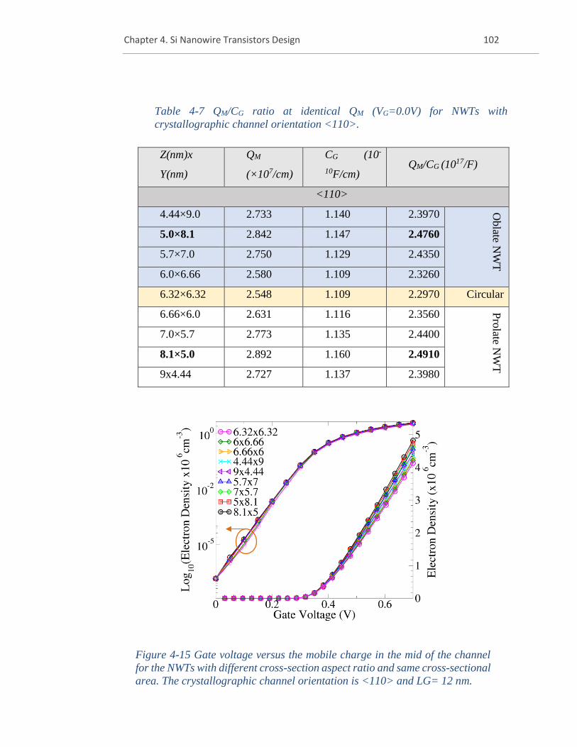
Chapter 4. Si Nanowire Transistors Design 102
Table 4-7 QM/CG ratio at identical QM (VG=0.0V) for NWTs with
crystallographic channel orientation <110>.
Z(nm)x
Y(nm)
QM
(×107/cm)
CG (10-
10F/cm) QM/CG (1017/F)
<110>
4.44×9.0 2.733 1.140 2.3970
Oblate N
WT
5.0×8.1 2.842 1.147 2.4760
5.7×7.0 2.750 1.129 2.4350
6.0×6.66 2.580 1.109 2.3260
6.32×6.32 2.548 1.109 2.2970 Circular
6.66×6.0 2.631 1.116 2.3560
Pro
late NW
T
7.0×5.7 2.773 1.135 2.4400
8.1×5.0 2.892 1.160 2.4910
9x4.44 2.727 1.137 2.3980
Figure 4-15 Gate voltage versus the mobile charge in the mid of the channel
for the NWTs with different cross-section aspect ratio and same cross-sectional
area. The crystallographic channel orientation is <110> and LG= 12 nm.
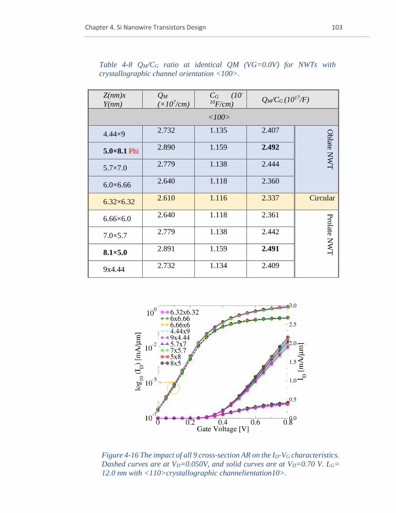
Chapter 4. Si Nanowire Transistors Design 103
Table 4-8 QM/CG ratio at identical QM (VG=0.0V) for NWTs with
crystallographic channel orientation <100>.
Z(nm)x
Y(nm)
QM
(×107/cm)
CG (10-
10F/cm) QM/CG (1017/F)
<100>
4.44×9 2.732 1.135 2.407
Oblate N
WT
5.0×8.1 Phi 2.890 1.159 2.492
5.7×7.0 2.779 1.138 2.444
6.0×6.66 2.640 1.118 2.360
6.32×6.32 2.610 1.116 2.337 Circular
6.66×6.0 2.640 1.118 2.361
Pro
late NW
T
7.0×5.7 2.779 1.138 2.442
8.1×5.0 2.891 1.159 2.491
9x4.44 2.732 1.134 2.409
Figure 4-16 The impact of all 9 cross-section AR on the ID-VG characteristics.
Dashed curves are at VD=0.050V, and solid curves are at VD=0.70 V. LG=
12.0 nm with <110>crystallographic channelientation10>.
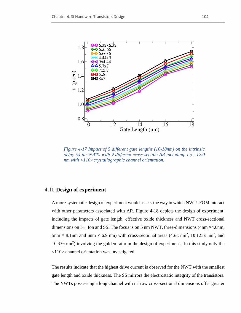
Chapter 4. Si Nanowire Transistors Design 104
Design of experiment
A more systematic design of experiment would assess the way in which NWTs FOM interact
with other parameters associated with AR. Figure 4-18 depicts the design of experiment,
including the impacts of gate length, effective oxide thickness and NWT cross-sectional
dimensions on Ioff, Ion and SS. The focus is on 5 nm NWT, three-dimensions (4nm ×4.6nm,
5nm × 8.1nm and 6nm × 6.9 nm) with cross-sectional areas (4.6π nm2, 10.125π nm2, and
10.35π nm2) involving the golden ratio in the design of experiment. In this study only the
<110> channel orientation was investigated.
The results indicate that the highest drive current is observed for the NWT with the smallest
gate length and oxide thickness. The SS mirrors the electrostatic integrity of the transistors.
The NWTs possessing a long channel with narrow cross-sectional dimensions offer greater
Figure 4-17 Impact of 5 different gate lengths (10-18nm) on the intrinsic
delay (τ) for NWTs with 9 different cross-section AR including. LG= 12.0
nm with <110>crystallographic channel orientation.
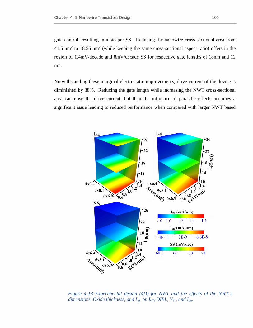
Chapter 4. Si Nanowire Transistors Design 105
gate control, resulting in a steeper SS. Reducing the nanowire cross-sectional area from
41.5 nm2 to 18.56 nm2 (while keeping the same cross-sectional aspect ratio) offers in the
region of 1.4mV/decade and 8mV/decade SS for respective gate lengths of 18nm and 12
nm.
Notwithstanding these marginal electrostatic improvements, drive current of the device is
diminished by 38%. Reducing the gate length while increasing the NWT cross-sectional
area can raise the drive current, but then the influence of parasitic effects becomes a
significant issue leading to reduced performance when compared with larger NWT based
Figure 4-18 Experimental design (4D) for NWT and the effects of the NWT’s
dimensions, Oxide thickness, and Lg on Ioff, DIBL, VT , and Ion.
Chapter 4. Si Nanowire Transistors Design 106
devices. The NWT with gate dimensions 12nm-16nm exhibits an acceptable trade-off
between the Ion, Ioff and SS.
Conclusions
The quantum mechanical impact on the electrostatic performance of NWTs suitable for
CMOS technologies at and beyond 5-nm mark have been investigated. It has been
highlighted how the shape of NWT influences the gate capacitance and the mobile charge
in the channel. Furthermore, circular and elliptical NWT, with channel orientations <110>
and <100>, have been investigated showing enhanced performance (with respect to
electrostatic driven performance and ‘intrinsic’ (QM/CG) ratio) when compared with square
and rectangular ultra-scaled GAA NWTs. For instance, the circular and elliptical nanowires
exhibit a greater quantum mobile charge (QM) in the channel and also a higher (QM/CG) ratio
compared to the square and rectangular nanowires. In addition, the results show that the 2D
charge profile and the quantity of charge in the channel depend on the channel direction.
For instance, all nanowires with the <100> channel have approximately ~11% greater
mobile charge compared to the <110> nanowires. Such findings are important for
determining the optimal designs of NWTs. Signatures of isotropic charge distributions
within Si NWTs were observed exhibiting the same attributes as the golden ratio (Phi), the
significance of which is well known in the fields of art and architecture.
The research demonstrates that the quantity of mobile charge within the channel, along with
the intrinsic speed of the device are determined by device geometry and may be affiliated
with the golden AR (Phi) of the nanowire transistors. This investigation has demonstrated
NWT with aspect ratios equal or close to the golden ratio (Phi) can enhance gate capacitance
and mobile charge in the channel and therefore could optimise the intrinsic speed of the
device. We have also investigated the influences of the gate length on the time delay and
the main FoM, such as VT, IOFF and ION and DIBL.
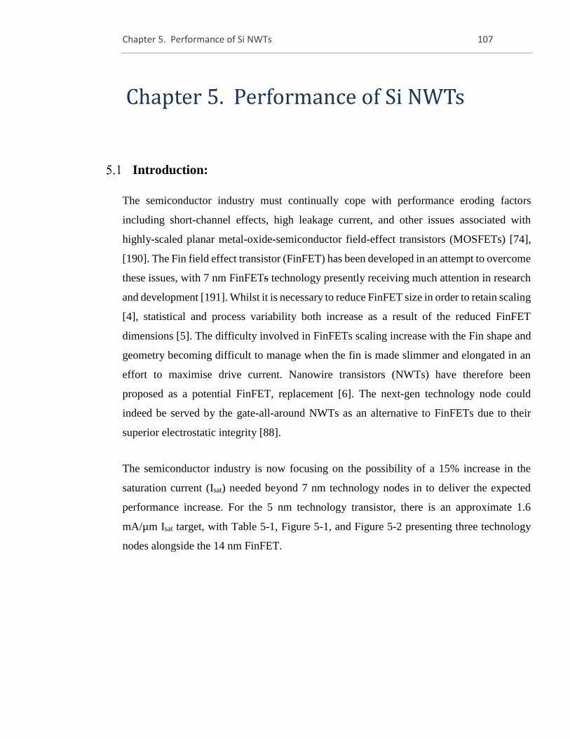
Chapter 5. Performance of Si NWTs 107
5 Chapter 5. Performance of Si NWTs
Introduction:
The semiconductor industry must continually cope with performance eroding factors
including short-channel effects, high leakage current, and other issues associated with
highly-scaled planar metal-oxide-semiconductor field-effect transistors (MOSFETs) [74],
[190]. The Fin field effect transistor (FinFET) has been developed in an attempt to overcome
these issues, with 7 nm FinFETs technology presently receiving much attention in research
and development [191]. Whilst it is necessary to reduce FinFET size in order to retain scaling
[4], statistical and process variability both increase as a result of the reduced FinFET
dimensions [5]. The difficulty involved in FinFETs scaling increase with the Fin shape and
geometry becoming difficult to manage when the fin is made slimmer and elongated in an
effort to maximise drive current. Nanowire transistors (NWTs) have therefore been
proposed as a potential FinFET, replacement [6]. The next-gen technology node could
indeed be served by the gate-all-around NWTs as an alternative to FinFETs due to their
superior electrostatic integrity [88].
The semiconductor industry is now focusing on the possibility of a 15% increase in the
saturation current (Isat) needed beyond 7 nm technology nodes in to deliver the expected
performance increase. For the 5 nm technology transistor, there is an approximate 1.6
mA/µm Isat target, with Table 5-1, Figure 5-1, and Figure 5-2 presenting three technology
nodes alongside the 14 nm FinFET.
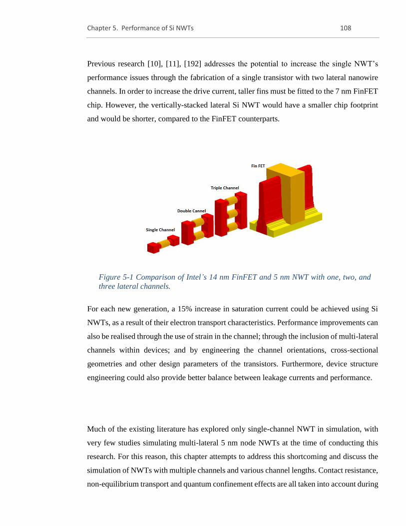
Chapter 5. Performance of Si NWTs 108
Previous research [10], [11], [192] addresses the potential to increase the single NWT’s
performance issues through the fabrication of a single transistor with two lateral nanowire
channels. In order to increase the drive current, taller fins must be fitted to the 7 nm FinFET
chip. However, the vertically-stacked lateral Si NWT would have a smaller chip footprint
and would be shorter, compared to the FinFET counterparts.
For each new generation, a 15% increase in saturation current could be achieved using Si
NWTs, as a result of their electron transport characteristics. Performance improvements can
also be realised through the use of strain in the channel; through the inclusion of multi-lateral
channels within devices; and by engineering the channel orientations, cross-sectional
geometries and other design parameters of the transistors. Furthermore, device structure
engineering could also provide better balance between leakage currents and performance.
Much of the existing literature has explored only single-channel NWT in simulation, with
very few studies simulating multi-lateral 5 nm node NWTs at the time of conducting this
research. For this reason, this chapter attempts to address this shortcoming and discuss the
simulation of NWTs with multiple channels and various channel lengths. Contact resistance,
non-equilibrium transport and quantum confinement effects are all taken into account during
Figure 5-1 Comparison of Intel’s 14 nm FinFET and 5 nm NWT with one, two, and
three lateral channels.
Chapter 5. Performance of Si NWTs 109
the simulations in order to provide reliable and accurate results appropriate for highly-scaled
NWTs. Importantly, this chapter also aims to address two main questions: firstly, whether
a single-channel silicon (NWT) at 5 nm technology node is able to achieve the
semiconductor industry target; and, secondly, if this is not possible, what number of
nanowire channels are required in a single NWT is in order to reach this target.
The following section of this chapter describes the device, whilst the simulation
methodology is presented in Section 5.3. Section 5.4 discusses the calibration methodology.
The results are presented in Section 5.5 and Section 5.6. Finally, conclusions from the
simulation are presented in Section 5.7.
Figure 5-2 Saturation current scaling target from 14 nm to 5 nm technology.
Table 5-1 Layout pitch and corresponding saturation current for(14-5nm)
technology.
Node 14 nm 10 nm 7 nm 5 nm
Layout pitch 42nm 29nm 21nm 14nm
Isat x15% (mA/um) 1.040 1.1960 1.3750 1.580
Chapter 5. Performance of Si NWTs 110
Device Description:
The previous chapter elucidated the relationship between performance, electrostatic
integrity, quantum effects and cross-sectional geometry in highly-scaled NWTs. The results
demonstrate that the strongest performance is found in NWTs with elliptical cross-sections
compared to the performance NWTs with circular and square cross-sections.
The current section analyses the performance of Si n-channel gate-all-around NWTs with
elliptical 7 nm x 5 nm and 8.1 nm x 5 nm cross-sections. Each of the simulated devices has
a 0.4nm SiO2 interfacial and 0.8nm HfO2 (High-k) gate dielectric layers. As illustrated in
Figure 4-5 and 4-6, doping concentrations of - 1014/cm3, 1020/cm3 and 4x10²⁰/cm3 were used
in the channel, extensions and source/drain, respectively. The study includes simulation of
10 nm, 12 nm, 16 nm and 20 nm gate length NWTs, with single-, double- and triple-
channels. The source/drain contacts were set at the tops of the devices in each case (see
Figure 4-5) for overall device structure).
Ensemble Monte Carlo (EMC) Simulation:
Charge transport and performance of a single nanowire NWT was analysed using Ensemble
Monte Carlo (EMC) simulations including band structure, relevant scattering mechanisms
[193], [194], volume inversion [195], and other physical relevant for Si NWT scaled below
14 nm. As a result of the impact of confined acoustic phonon and body thickness variation-
induced scattering [101], a rapid reduction in mobility been observed below 4 nm. Extensive
downward scaling of NWT thickness has also been achieved, with a near-5 nm nanowire
diameter. Significant quantization effects can observed in the nanowire cross-section, as a
result of a high electric field and small confinement dimensions [196]. Consequently,
discrete sub-bands are formed from the conduction band, with the maximum charge density
trends shifting towards the channel centre and away from the metal-oxide interface. These
quantum effects impact device properties and should therefore be taken into account when
analysing device performance. Thus, in this study, the impact of quantum confinement
Chapter 5. Performance of Si NWTs 111
effects on saturation current are explored using a self-consistent three-dimensional quantum
mechanical Monte Carlo (3D-MC) simulator. The primary benefit of quantum-corrected 3D-
MC simulation approach is the ability to simulate the quantum effects across the entire NWT
structure. Furthermore, this approach also takes into account the transition of electrons
between quantized states, resulting in greater accuracy when self-consistently calculating
nonequilibrium electron distribution and current.
The MC method provides a direct solution to the Boltzmann transport equation (BTE), and
therefore can capture non-equilibrium, quasi ballistic transport in nanometre scale
semiconductor devices. It is suitable to apply to the simulation of Fin-FET, nanowire
transistors and other novel 3D transistors. Furthermore, it is more accurate and predictive
compared to drift-diffusion (DD) simulations. The smaller the transistor the more non-
equilibrium the transport becomes with carrier heating [197] and with an increasingly
significant velocity overshoot as a non-local effect.
The Ensemble Monte Carlo (EMC) [198] approach with Poisson-Schrödinger (PS) quantum
corrections was adopted for the purpose of these simulations. As mentioned before the
Monte Carlo approach provides a direct solution to the BTE. The method takes into account
key electron scattering mechanisms such as intra- and inter-valley electron-phonon
scatterings, surface roughness scattering, ionised impurity scattering, and the stochastic
characteristics of electron transport. The k·p method was also utilised to calculate a full-
band structure, which was approximated with and analytical band structure model comprised
of ellipsoidal non-parabolic valleys. The movement of hundreds of thousands of particles
within a field distribution was tracked in order to achieve self-consistent simulation, with
Poisson’s equation solved in 3D every 0.50 fs. The 3D-EMC simulation began with initial
conditions set as the DD solution and the corresponding potential profiles and charge
distribution. During simulation, self-consistent time-varying electrostatic potential and field
distributions were upheld through the solution of the linear Poisson equation and the
application of QM correction. In highly-scaled channel transistors, the 3D-EMC simulation
approach has been shown to offer high levels of accuracy in forecasting ON-state transistor
performance and in the handling of non-equilibrium transport [199].
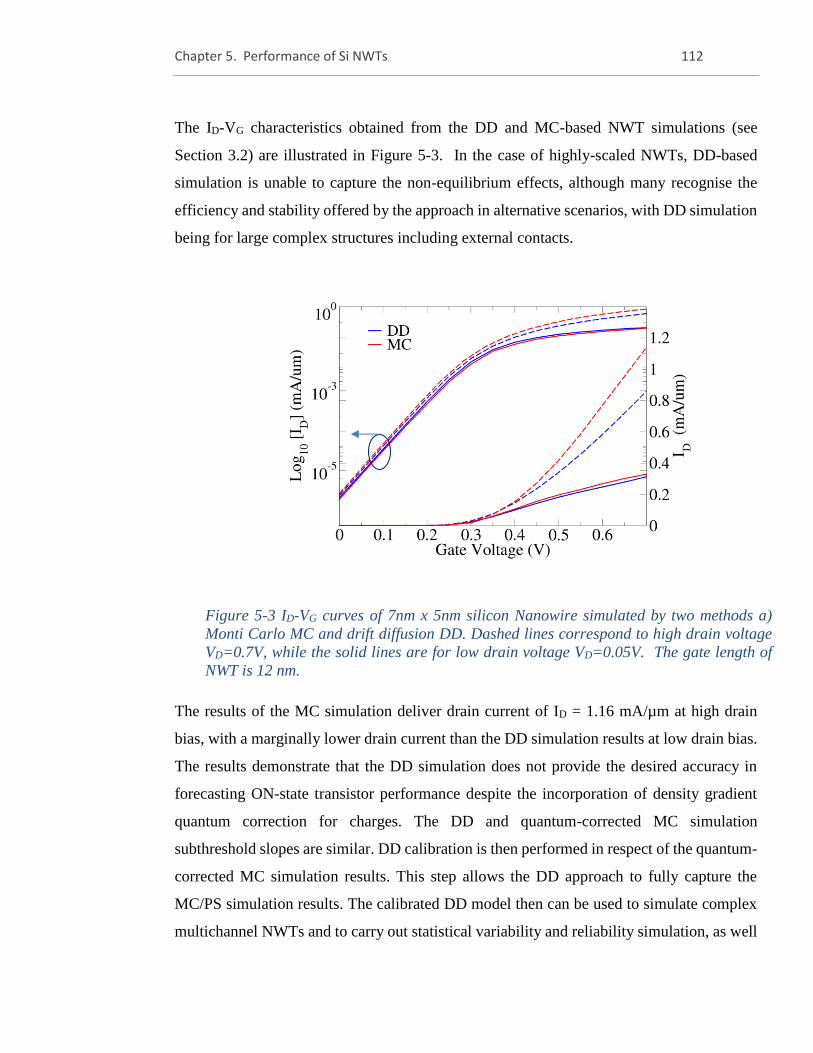
Chapter 5. Performance of Si NWTs 112
The ID-VG characteristics obtained from the DD and MC-based NWT simulations (see
Section 3.2) are illustrated in Figure 5-3. In the case of highly-scaled NWTs, DD-based
simulation is unable to capture the non-equilibrium effects, although many recognise the
efficiency and stability offered by the approach in alternative scenarios, with DD simulation
being for large complex structures including external contacts.
The results of the MC simulation deliver drain current of ID = 1.16 mA/µm at high drain
bias, with a marginally lower drain current than the DD simulation results at low drain bias.
The results demonstrate that the DD simulation does not provide the desired accuracy in
forecasting ON-state transistor performance despite the incorporation of density gradient
quantum correction for charges. The DD and quantum-corrected MC simulation
subthreshold slopes are similar. DD calibration is then performed in respect of the quantum-
corrected MC simulation results. This step allows the DD approach to fully capture the
MC/PS simulation results. The calibrated DD model then can be used to simulate complex
multichannel NWTs and to carry out statistical variability and reliability simulation, as well
Figure 5-3 ID-VG curves of 7nm x 5nm silicon Nanowire simulated by two methods a)
Monti Carlo MC and drift diffusion DD. Dashed lines correspond to high drain voltage
VD=0.7V, while the solid lines are for low drain voltage VD=0.05V. The gate length of
NWT is 12 nm.
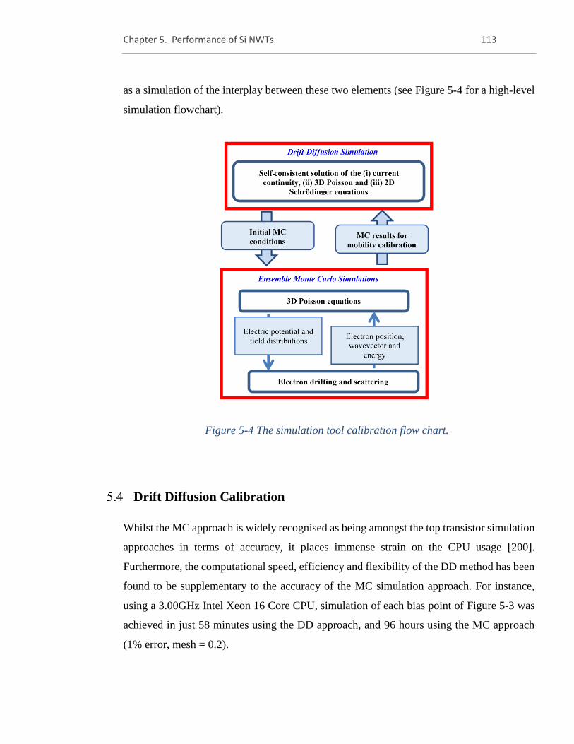
Chapter 5. Performance of Si NWTs 113
as a simulation of the interplay between these two elements (see Figure 5-4 for a high-level
simulation flowchart).
Drift Diffusion Calibration
Whilst the MC approach is widely recognised as being amongst the top transistor simulation
approaches in terms of accuracy, it places immense strain on the CPU usage [200].
Furthermore, the computational speed, efficiency and flexibility of the DD method has been
found to be supplementary to the accuracy of the MC simulation approach. For instance,
using a 3.00GHz Intel Xeon 16 Core CPU, simulation of each bias point of Figure 5-3 was
achieved in just 58 minutes using the DD approach, and 96 hours using the MC approach
(1% error, mesh = 0.2).
Figure 5-4 The simulation tool calibration flow chart.
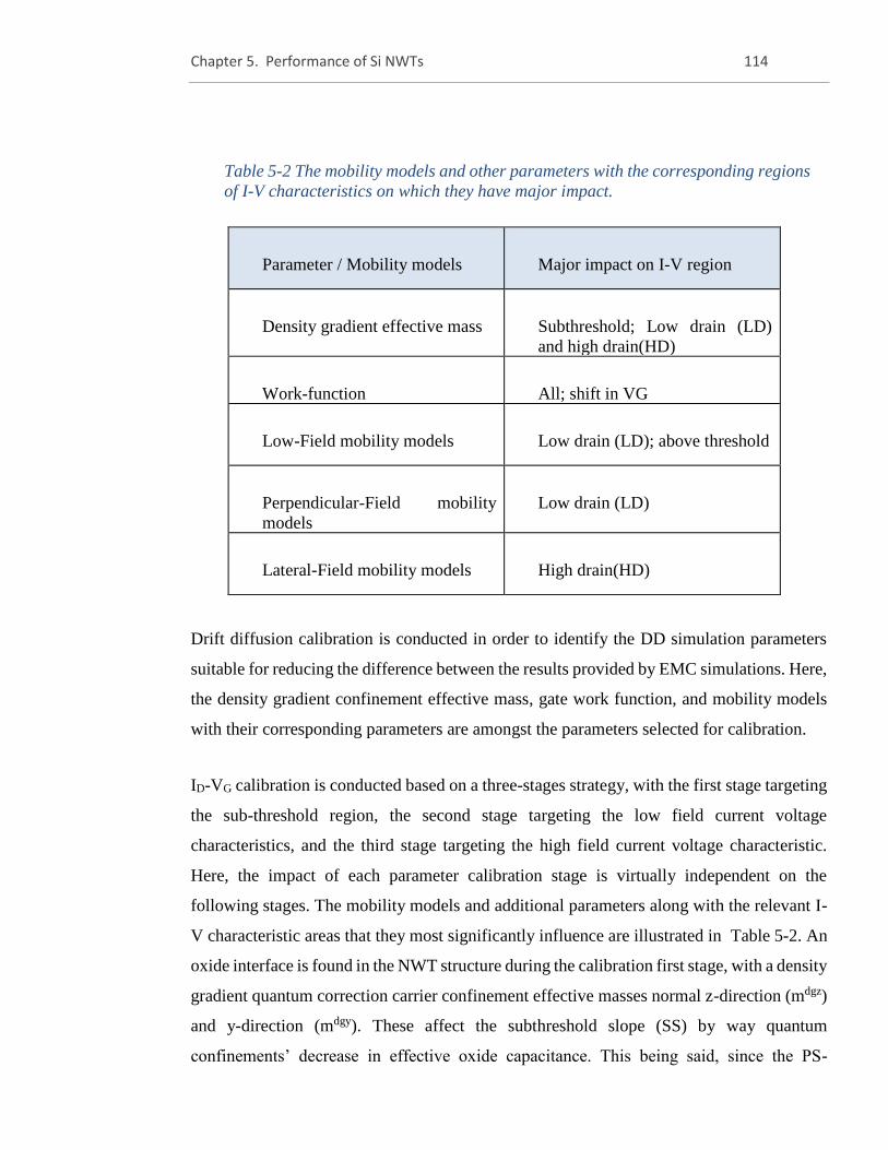
Chapter 5. Performance of Si NWTs 114
Drift diffusion calibration is conducted in order to identify the DD simulation parameters
suitable for reducing the difference between the results provided by EMC simulations. Here,
the density gradient confinement effective mass, gate work function, and mobility models
with their corresponding parameters are amongst the parameters selected for calibration.
ID-VG calibration is conducted based on a three-stages strategy, with the first stage targeting
the sub-threshold region, the second stage targeting the low field current voltage
characteristics, and the third stage targeting the high field current voltage characteristic.
Here, the impact of each parameter calibration stage is virtually independent on the
following stages. The mobility models and additional parameters along with the relevant I-
V characteristic areas that they most significantly influence are illustrated in Table 5-2. An
oxide interface is found in the NWT structure during the calibration first stage, with a density
gradient quantum correction carrier confinement effective masses normal z-direction (mdgz)
and y-direction (mdgy). These affect the subthreshold slope (SS) by way quantum
confinements’ decrease in effective oxide capacitance. This being said, since the PS-
Table 5-2 The mobility models and other parameters with the corresponding regions
of I-V characteristics on which they have major impact.
Parameter / Mobility models Major impact on I-V region
Density gradient effective mass Subthreshold; Low drain (LD)
and high drain(HD)
Work-function All; shift in VG
Low-Field mobility models Low drain (LD); above threshold
Perpendicular-Field mobility
models
Low drain (LD)
Lateral-Field mobility models High drain(HD)
Chapter 5. Performance of Si NWTs 115
calibration of the density gradient effective masses has already been carried out, it does not
need to be changed at this stage. Modification of the work function at any of the calibration
stages realigns the VT.
In the (Poisson-Schrödinger (PS) / Drift-Diffusion (DD)) simulation, up to three mobility
models can be selected to use in a given simulation: 1) Low-field mobility (that considers
ionized impurity scattering); Arora mobility model [149], Masetti mobility model [148], and
Philips mobility model [150]. 2)Perpendicular field-dependent mobility (that considers
surface roughness scattering); Yamaguchi [151], Lombardi [152], and thin-layer mobility
model [153]. 3) Lateral field-dependent mobility (for velocity saturation); Caughey-Thomas
velocity saturation model [154]. In this work, the following three carrier mobility models
have been used, Masetti, Lombardi, and Caughey-Thomas. At low VD, the NWT ID-VG
characteristics are determined by the low-field mobility for a gate voltage around and just
above VT. then the device calibration process is the calibration of the complete ID-VG
characteristics at low drain bias. During the 1st calibration iteration a perpendicular electric
field model has been activated and the lateral electric field model disabled. In the final stage
of the calibration process, the complete ID-VG behaviour at high applied VD is calibrated.
During the first calibration iteration a lateral electric field model has been enabled and the
perpendicular electric field model disabled. At all stages of the calibration the VT can be
realigned by modifying the work function.
5nm NWT: MC simulation
Simulations of the ID-VG characteristics of the NWTs under consideration are carried out
following the aforementioned methodology. The ID-VG characteristics of a 14 nm FinFET
transistor is compared to that of a single Si-NWT simulation in Figure 5-5, with the results
benchmarked against the 5 nm CMOS’ target drive current of 1.58 mA/µm. This was
justified during the introduction. Alignment of the two characteristics provides the same
leakage current. The results demonstrate that the 14 nm FinFET has a lower Iast than the
single nanowire transistor at both high and low drain biases. Here, SS is approximately 62.55
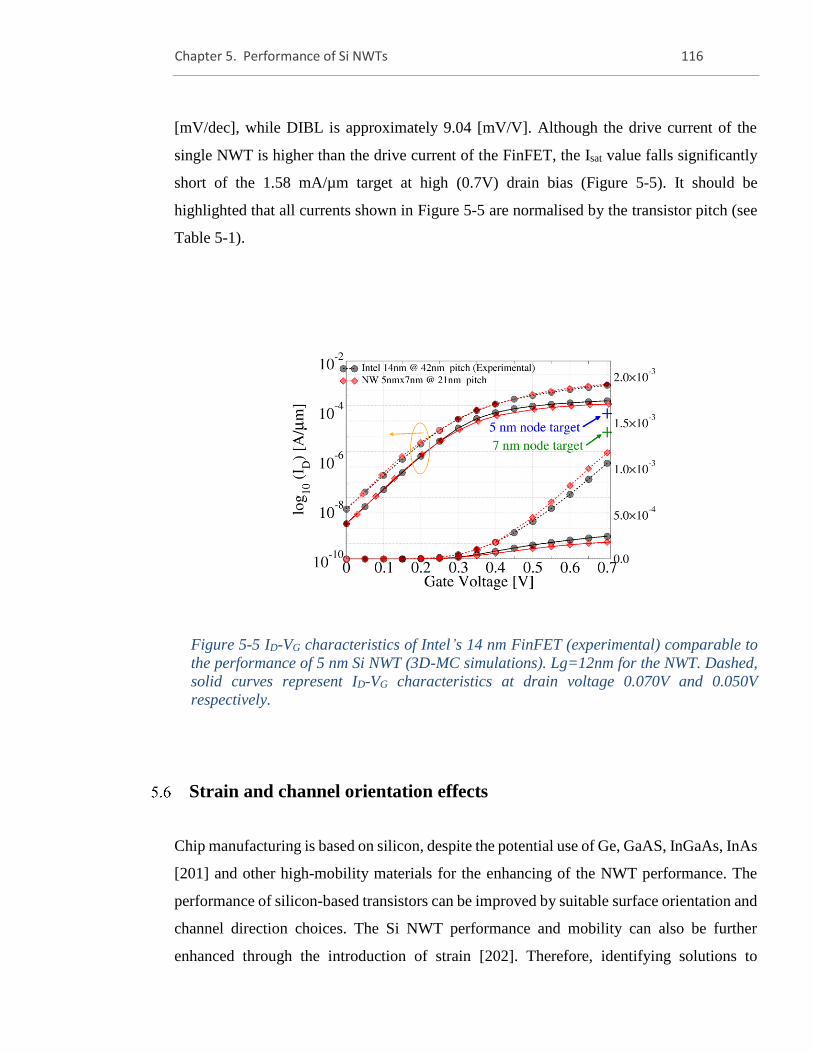
Chapter 5. Performance of Si NWTs 116
[mV/dec], while DIBL is approximately 9.04 [mV/V]. Although the drive current of the
single NWT is higher than the drive current of the FinFET, the Isat value falls significantly
short of the 1.58 mA/µm target at high (0.7V) drain bias (Figure 5-5). It should be
highlighted that all currents shown in Figure 5-5 are normalised by the transistor pitch (see
Table 5-1).
Strain and channel orientation effects
Chip manufacturing is based on silicon, despite the potential use of Ge, GaAS, InGaAs, InAs
[201] and other high-mobility materials for the enhancing of the NWT performance. The
performance of silicon-based transistors can be improved by suitable surface orientation and
channel direction choices. The Si NWT performance and mobility can also be further
enhanced through the introduction of strain [202]. Therefore, identifying solutions to
Figure 5-5 ID-VG characteristics of Intel’s 14 nm FinFET (experimental) comparable to
the performance of 5 nm Si NWT (3D-MC simulations). Lg=12nm for the NWT. Dashed,
solid curves represent ID-VG characteristics at drain voltage 0.070V and 0.050V
respectively.
Chapter 5. Performance of Si NWTs 117
achieve the highest strain levels possible at the present time is a high priority for the
semiconductor industry. Recent research reports a successful attempt to move significantly
beyond the limits of SiGe-based virtual substrates by using a 4.5% elastic strain of 7.6 GPa
uniaxial tensile stress in Si nanowires with a width of 30 nm [203]. In traditional FETs, high
STI-based compressive stress result in a saturation current of scaled <110> nFETs being
close to <100> nFETs. The velocity saturation of <110> pFETs is lower than that of nFETs,
with mobility also being higher in <110> pFETs compared to <100> pFETs, rendering the
scaled <110> pFETs more preferable [204]. Significant research is focused on <110>
surface orientation, which has been heavily adopted in gate-all-around FETs, FinFETs and
other FET structures [205].
Extreme downward scaling of NWT diameter to 5 nm has been achieved. Significant
quantization effects can be seen in the corresponding NWTs. , [196]. Consequently, discrete
sub-bands are formed from the conduction band, with the maximum charge density shifting
towards the channel centre and away from the metal-oxide interface. It is also possible for
the charge density to have an isotropic distribution. These quantum effects have an impact
on device performance and must therefore be taken into account during device simulation
analysis. Therefore, this study investigates the impact of the quantum mechanical effects on
the NWTs saturation current using a self-consistent three-dimensional quantum mechanical
Monte Carlo (3D-MC) simulation approach. The ability of the quantum-corrected 3D-MC
approach to capture accurately the quantum effects is one of the main advantage of this
approach.
We begin by analysing 7 nm x 5 nm NWTs with channel orientations of <110> and <100>
with regards to strain impact. Here, axis rotation necessitates that each valley’s effective
mass tensor must be converted, and thus the impact of switching between the <110> to
<100> channel orientation without strain must be assessed first.
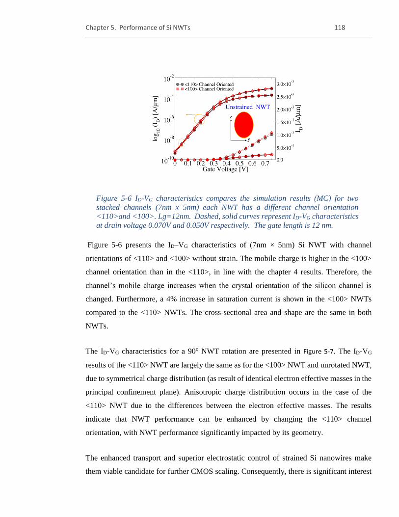
Chapter 5. Performance of Si NWTs 118
Figure 5-6 presents the ID–VG characteristics of (7nm × 5nm) Si NWT with channel
orientations of <110> and <100> without strain. The mobile charge is higher in the <100>
channel orientation than in the <110>, in line with the chapter 4 results. Therefore, the
channel’s mobile charge increases when the crystal orientation of the silicon channel is
changed. Furthermore, a 4% increase in saturation current is shown in the <100> NWTs
compared to the <110> NWTs. The cross-sectional area and shape are the same in both
NWTs.
The ID-VG characteristics for a 90o NWT rotation are presented in Figure 5-7. The ID-VG
results of the <110> NWT are largely the same as for the <100> NWT and unrotated NWT,
due to symmetrical charge distribution (as result of identical electron effective masses in the
principal confinement plane). Anisotropic charge distribution occurs in the case of the
<110> NWT due to the differences between the electron effective masses. The results
indicate that NWT performance can be enhanced by changing the <110> channel
orientation, with NWT performance significantly impacted by its geometry.
The enhanced transport and superior electrostatic control of strained Si nanowires make
them viable candidate for further CMOS scaling. Consequently, there is significant interest
Figure 5-6 ID-VG characteristics compares the simulation results (MC) for two
stacked channels (7nm x 5nm) each NWT has a different channel orientation
<110>and <100>. Lg=12nm. Dashed, solid curves represent ID-VG characteristics
at drain voltage 0.070V and 0.050V respectively. The gate length is 12 nm.
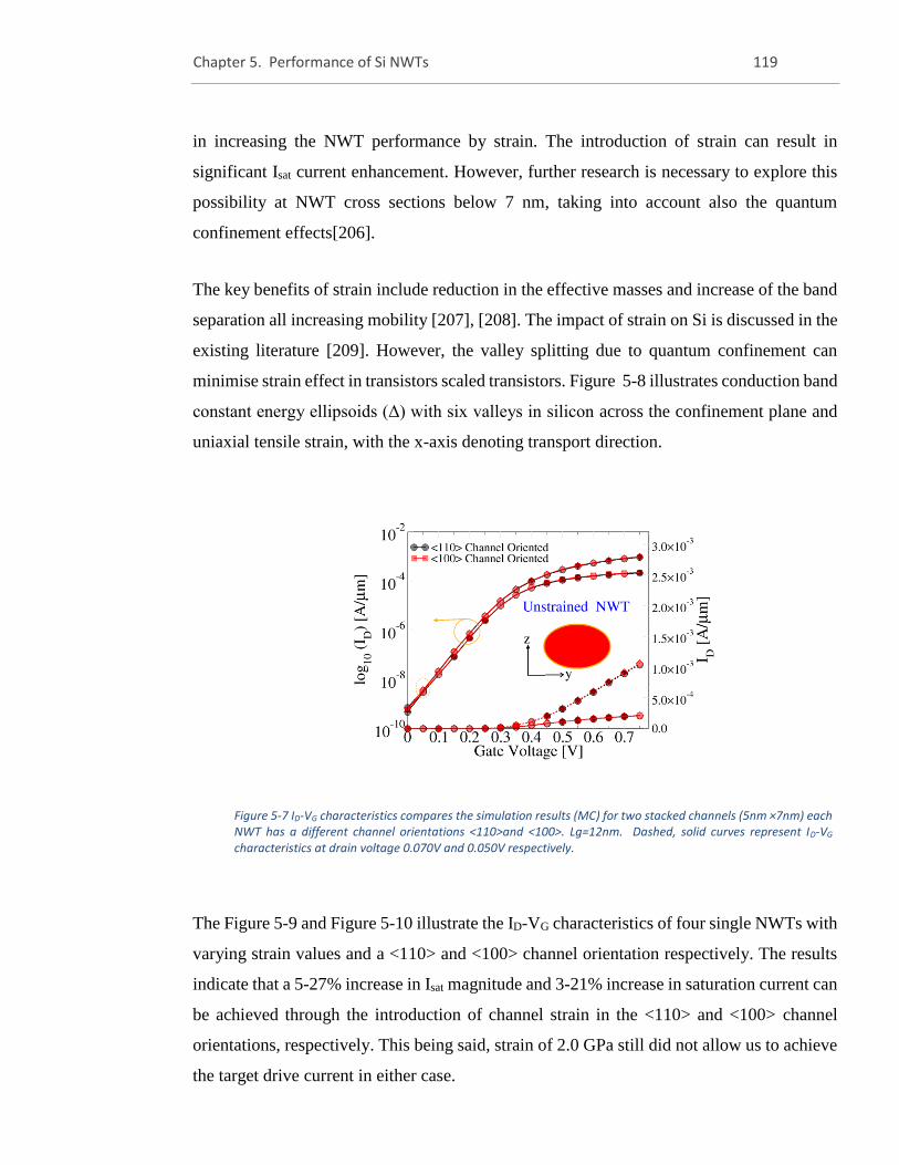
Chapter 5. Performance of Si NWTs 119
in increasing the NWT performance by strain. The introduction of strain can result in
significant Isat current enhancement. However, further research is necessary to explore this
possibility at NWT cross sections below 7 nm, taking into account also the quantum
confinement effects[206].
The key benefits of strain include reduction in the effective masses and increase of the band
separation all increasing mobility [207], [208]. The impact of strain on Si is discussed in the
existing literature [209]. However, the valley splitting due to quantum confinement can
minimise strain effect in transistors scaled transistors. Figure 5-8 illustrates conduction band
constant energy ellipsoids (Δ) with six valleys in silicon across the confinement plane and
uniaxial tensile strain, with the x-axis denoting transport direction.
The Figure 5-9 and Figure 5-10 illustrate the ID-VG characteristics of four single NWTs with
varying strain values and a <110> and <100> channel orientation respectively. The results
indicate that a 5-27% increase in Isat magnitude and 3-21% increase in saturation current can
be achieved through the introduction of channel strain in the <110> and <100> channel
orientations, respectively. This being said, strain of 2.0 GPa still did not allow us to achieve
the target drive current in either case.
Figure 5-7 ID-VG characteristics compares the simulation results (MC) for two stacked channels (5nm ×7nm) each NWT has a different channel orientations <110>and <100>. Lg=12nm. Dashed, solid curves represent ID-VG characteristics at drain voltage 0.070V and 0.050V respectively.
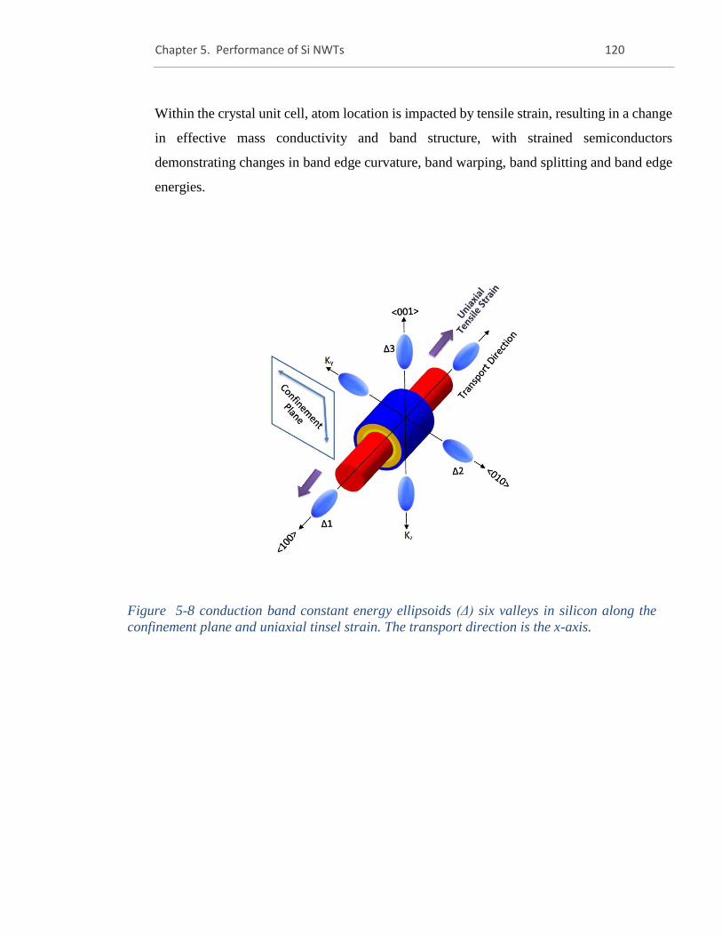
Chapter 5. Performance of Si NWTs 120
Within the crystal unit cell, atom location is impacted by tensile strain, resulting in a change
in effective mass conductivity and band structure, with strained semiconductors
demonstrating changes in band edge curvature, band warping, band splitting and band edge
energies.
Figure 5-8 conduction band constant energy ellipsoids (Δ) six valleys in silicon along the
confinement plane and uniaxial tinsel strain. The transport direction is the x-axis.
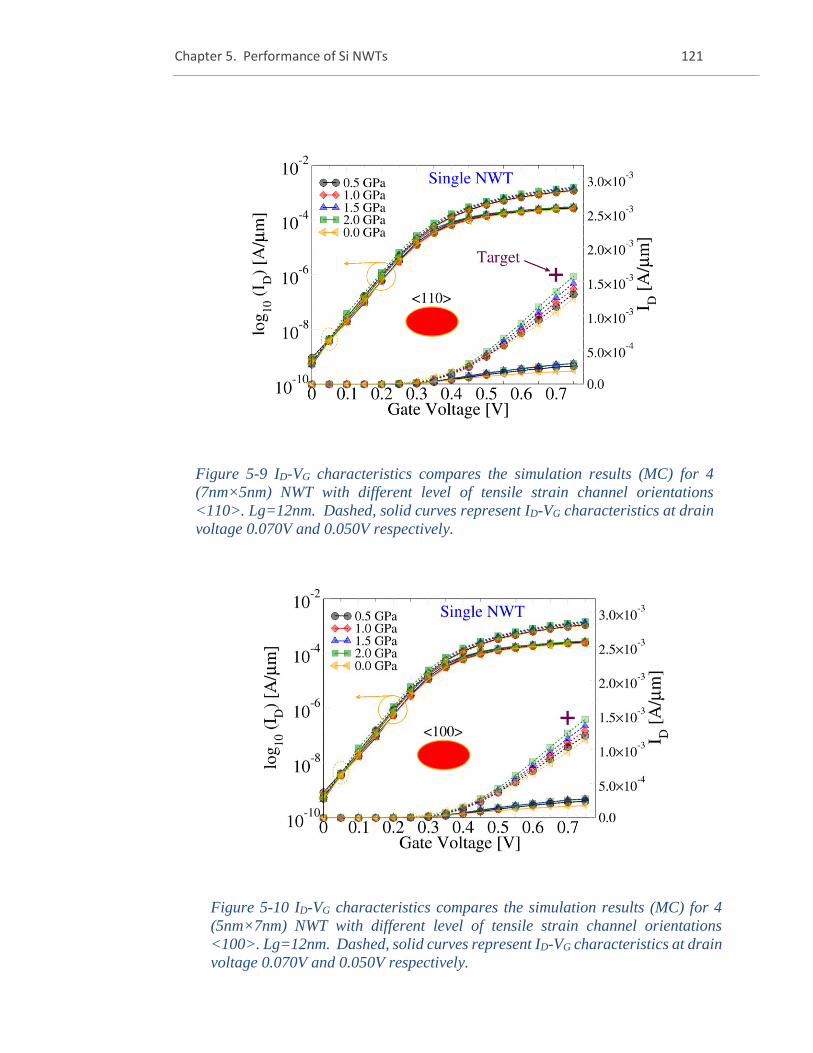
Chapter 5. Performance of Si NWTs 121
Figure 5-9 ID-VG characteristics compares the simulation results (MC) for 4
(7nm×5nm) NWT with different level of tensile strain channel orientations
<110>. Lg=12nm. Dashed, solid curves represent ID-VG characteristics at drain
voltage 0.070V and 0.050V respectively.
Figure 5-10 ID-VG characteristics compares the simulation results (MC) for 4
(5nm×7nm) NWT with different level of tensile strain channel orientations
<100>. Lg=12nm. Dashed, solid curves represent ID-VG characteristics at drain
voltage 0.070V and 0.050V respectively.
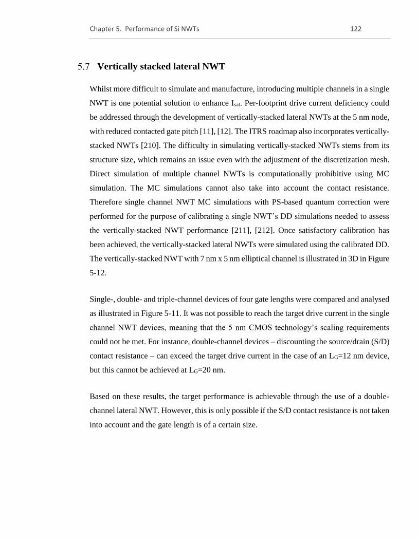
Chapter 5. Performance of Si NWTs 122
Vertically stacked lateral NWT
Whilst more difficult to simulate and manufacture, introducing multiple channels in a single
NWT is one potential solution to enhance Isat. Per-footprint drive current deficiency could
be addressed through the development of vertically-stacked lateral NWTs at the 5 nm node,
with reduced contacted gate pitch [11], [12]. The ITRS roadmap also incorporates vertically-
stacked NWTs [210]. The difficulty in simulating vertically-stacked NWTs stems from its
structure size, which remains an issue even with the adjustment of the discretization mesh.
Direct simulation of multiple channel NWTs is computationally prohibitive using MC
simulation. The MC simulations cannot also take into account the contact resistance.
Therefore single channel NWT MC simulations with PS-based quantum correction were
performed for the purpose of calibrating a single NWT’s DD simulations needed to assess
the vertically-stacked NWT performance [211], [212]. Once satisfactory calibration has
been achieved, the vertically-stacked lateral NWTs were simulated using the calibrated DD.
The vertically-stacked NWT with 7 nm x 5 nm elliptical channel is illustrated in 3D in Figure
5-12.
Single-, double- and triple-channel devices of four gate lengths were compared and analysed
as illustrated in Figure 5-11. It was not possible to reach the target drive current in the single
channel NWT devices, meaning that the 5 nm CMOS technology’s scaling requirements
could not be met. For instance, double-channel devices – discounting the source/drain (S/D)
contact resistance – can exceed the target drive current in the case of an LG=12 nm device,
but this cannot be achieved at LG=20 nm.
Based on these results, the target performance is achievable through the use of a double-
channel lateral NWT. However, this is only possible if the S/D contact resistance is not taken
into account and the gate length is of a certain size.
Chapter 5. Performance of Si NWTs 123
Compared to the 5 nm CMOS node target value of (15%) Isat current values are significantly
greater for the triple-channel lateral nanowires, as shown in Figure 5-11. Therefore, the
results indicate that the 5 nm CMOS scaling performance target could be safely achieved
through the introduction of three lateral channels stacked in a single NWT device. Still these
results do not take into account the S/D contact resistance.
Figure 5-12 3D schematic view of the vertically stacked NTW of two lateral channels
and material details.
Figure 5-11 Characteristics of the ID versus the VG obtained from calibrated DD for
the NWTs with one, two, and three channels. The DD is calibrated for each gate
lengths (10nm, 12nm,16nm, and 20nm). Dashed, solid curves represent ID-VG
characteristics at drain voltage 0.070V and 0.050V respectively.
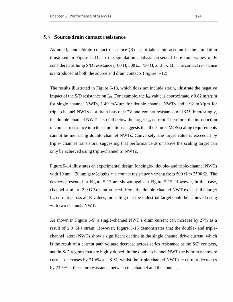
Chapter 5. Performance of Si NWTs 124
Source/drain contact resistance
As noted, source/drain contact resistance (R) is not taken into account in the simulation
illustrated in Figure 5-11. In the simulation analysis presented here four values of R
considered as lump S/D resistance (100 Ω, 500 Ω, 750 Ω, and 1K Ω). The contact resistance
is introduced at both the source and drain contacts (Figure 5-12).
The results illustrated in Figure 5-13, which does not include strain, illustrate the negative
impact of the S/D resistance on Isat. For example, the Isat value is approximately 0.82 mA/µm
for single-channel NWTs, 1.49 mA/µm for double-channel NWTs and 1.92 mA/µm for
triple-channel NWTs at a drain bias of 0.7V and contact resistance of 1KΩ. Interestingly,
the double-channel NWTs also fall below the target Isat current. Therefore, the introduction
of contact resistance into the simulations suggests that the 5 nm CMOS scaling requirements
cannot be met using double-channel NWTs. Conversely, the target value is exceeded by
triple- channel transistors, suggesting that performance at or above the scaling target can
only be achieved using triple-channel Si NWTs.
Figure 5-14 illustrates an experimental design for single-, double- and triple-channel NWTs
with 10 nm – 20 nm gate lengths at a contact resistance varying from 500 Ω to 2500 Ω. The
devices presented in Figure 5-13 are shown again in Figure 5-15. However, in this case,
channel strain of 2.0 GPa is introduced. Here, the double-channel NWT exceeds the target
Isat current across all R values, indicating that the industrial target could be achieved using
with two channels NWT.
As shown in Figure 5-9, a single-channel NWT’s drain current can increase by 27% as a
result of 2.0 GPa strain. However, Figure 5-15 demonstrates that the double- and triple-
channel lateral NWTs show a significant decline in the single channel drive current, which
is the result of a current path voltage decrease across series resistance at the S/D contacts,
and in S/D regions that are highly doped. In the double-channel NWT the bottom nanowire
current decreases by 21.6% at 1K Ω, whilst the triple-channel NWT the current decreases
by 23.5% at the same resistance, between the channel and the contact.
Chapter 5. Performance of Si NWTs 125
Current density: series resistance effect
The single-, double- and triple-channel NWTs’ current density is illustrated in 3D in Figure
5-16, which highlights the variance between current densities. Whilst the nanowires in the
triple-channel NWTs have the same cross-sectional area, current density is higher in the top
channel (nearest to the metal) compared to the lower and middle channels. This is
represented by the large red region near to the drain, with the red becoming weaker at the
second and third channels. Similar results are depicted for the double-channel device, with
greater current density in the top channel compared to the bottom channel. Therefore, the
results suggest that as the distance between the channel and the contact becomes greater, a
reduction in current density is experienced in each of the lateral channels.
Figure 5-13 Characteristics of the ID versus the VG obtained by calibrated DD for the
NWTs with one, two, and three channels at four different ohmic contact resistance.
Lg=12nm. Dashed, solid curves represent ID-VG characteristics at drain voltage 0.070V
and 0.050V respectively.
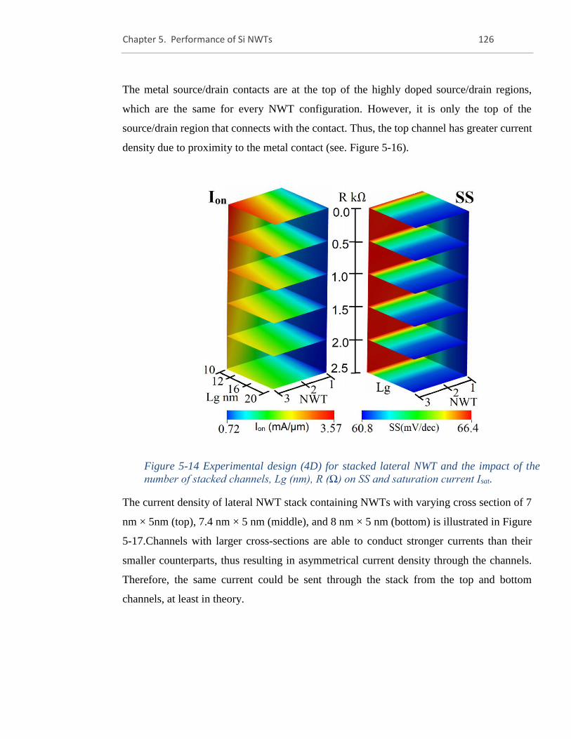
Chapter 5. Performance of Si NWTs 126
The metal source/drain contacts are at the top of the highly doped source/drain regions,
which are the same for every NWT configuration. However, it is only the top of the
source/drain region that connects with the contact. Thus, the top channel has greater current
density due to proximity to the metal contact (see. Figure 5-16).
The current density of lateral NWT stack containing NWTs with varying cross section of 7
nm × 5nm (top), 7.4 nm × 5 nm (middle), and 8 nm × 5 nm (bottom) is illustrated in Figure
5-17.Channels with larger cross-sections are able to conduct stronger currents than their
smaller counterparts, thus resulting in asymmetrical current density through the channels.
Therefore, the same current could be sent through the stack from the top and bottom
channels, at least in theory.
Figure 5-14 Experimental design (4D) for stacked lateral NWT and the impact of the
number of stacked channels, Lg (nm), R (Ω) on SS and saturation current Isat.
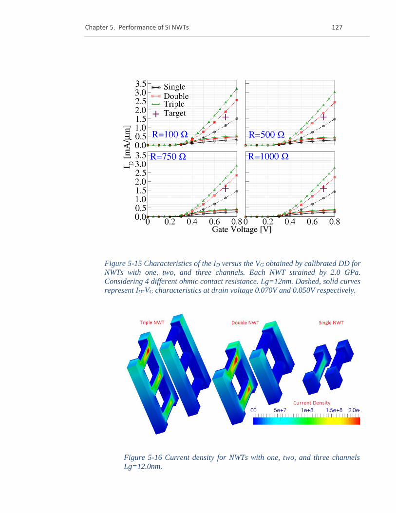
Chapter 5. Performance of Si NWTs 127
Figure 5-15 Characteristics of the ID versus the VG obtained by calibrated DD for
NWTs with one, two, and three channels. Each NWT strained by 2.0 GPa.
Considering 4 different ohmic contact resistance. Lg=12nm. Dashed, solid curves
represent ID-VG characteristics at drain voltage 0.070V and 0.050V respectively.
Figure 5-16 Current density for NWTs with one, two, and three channels
Lg=12.0nm.
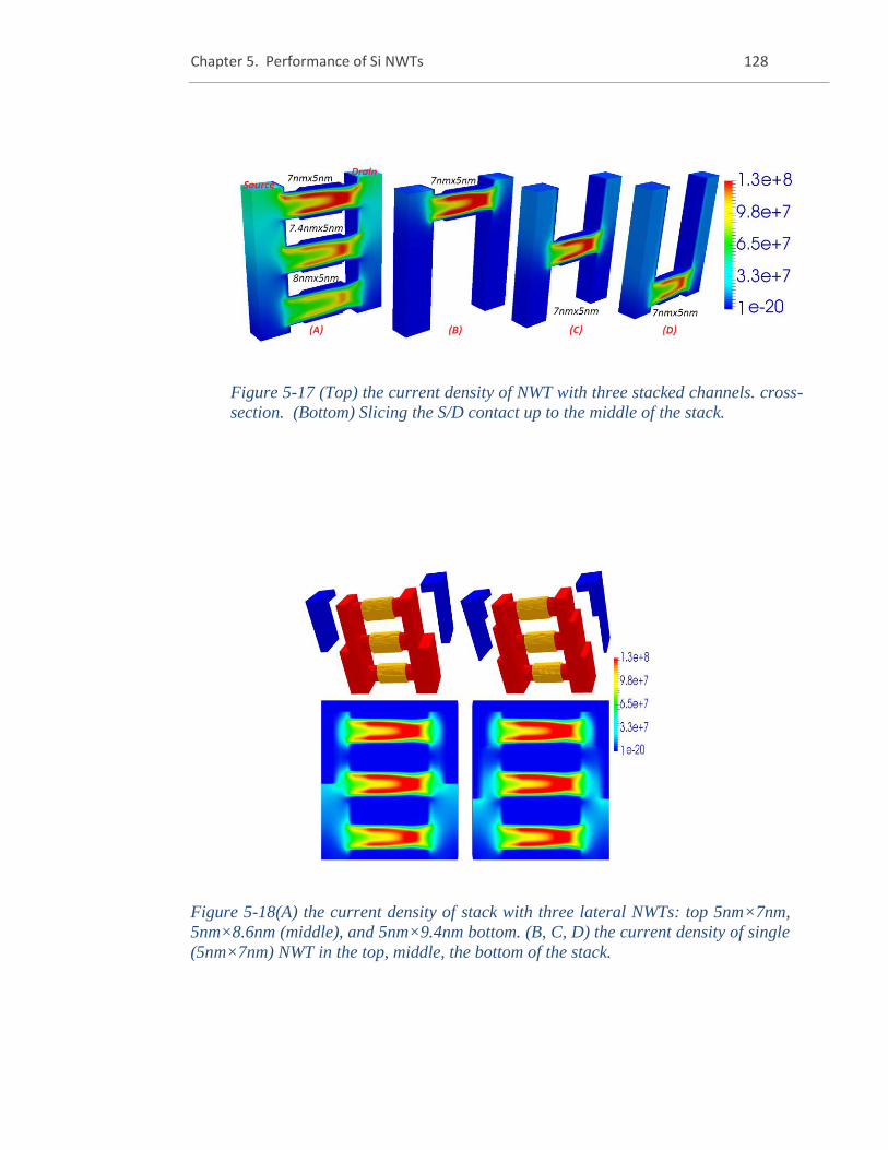
Chapter 5. Performance of Si NWTs 128
Figure 5-17 (Top) the current density of NWT with three stacked channels. cross-
section. (Bottom) Slicing the S/D contact up to the middle of the stack.
Figure 5-18(A) the current density of stack with three lateral NWTs: top 5nm×7nm,
5nm×8.6nm (middle), and 5nm×9.4nm bottom. (B, C, D) the current density of single
(5nm×7nm) NWT in the top, middle, the bottom of the stack.
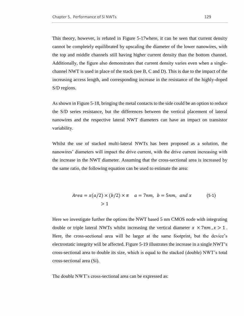
Chapter 5. Performance of Si NWTs 129
This theory, however, is refuted in Figure 5-17where, it can be seen that current density
cannot be completely equilibrated by upscaling the diameter of the lower nanowires, with
the top and middle channels still having higher current density than the bottom channel.
Additionally, the figure also demonstrates that current density varies even when a single-
channel NWT is used in place of the stack (see B, C and D). This is due to the impact of the
increasing access length, and corresponding increase in the resistance of the highly-doped
S/D regions.
As shown in Figure 5-18, bringing the metal contacts to the side could be an option to reduce
the S/D series resistance, but the differences between the vertical placement of lateral
nanowires and the respective lateral NWT diameters can have an impact on transistor
variability.
Whilst the use of stacked multi-lateral NWTs has been proposed as a solution, the
nanowires’ diameters will impact the drive current, with the drive current increasing with
the increase in the NWT diameter. Assuming that the cross-sectional area is increased by
the same ratio, the following equation can be used to estimate the area:
Here we investigate further the options the NWT based 5 nm CMOS node with integrating
double or triple lateral NWTs whilst increasing the vertical diameter 𝑥 × 7𝑛𝑚 , 𝑥 > 1 .
Here, the cross-sectional area will be larger at the same footprint, but the device’s
electrostatic integrity will be affected. Figure 5-19 illustrates the increase in a single NWT’s
cross-sectional area to double its size, which is equal to the stacked (double) NWT’s total
cross-sectional area (Si).
The double NWT’s cross-sectional area can be expressed as:
𝐴𝑟𝑒𝑎 = 𝑥(𝑎/2) × (𝑏/2) × 𝜋 𝑎 = 7𝑛𝑚, 𝑏 = 5𝑛𝑚, 𝑎𝑛𝑑 𝑥
> 1
(5-1)
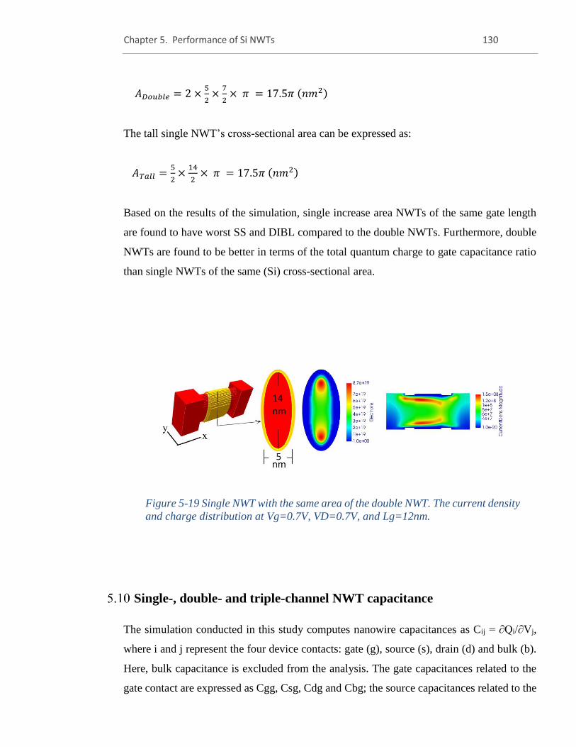
Chapter 5. Performance of Si NWTs 130
𝐴𝐷𝑜𝑢𝑏𝑙𝑒 = 2 ×5
2×
7
2× 𝜋 = 17.5𝜋 (𝑛𝑚2)
The tall single NWT’s cross-sectional area can be expressed as:
𝐴𝑇𝑎𝑙𝑙 =5
2×
14
2× 𝜋 = 17.5𝜋 (𝑛𝑚2)
Based on the results of the simulation, single increase area NWTs of the same gate length
are found to have worst SS and DIBL compared to the double NWTs. Furthermore, double
NWTs are found to be better in terms of the total quantum charge to gate capacitance ratio
than single NWTs of the same (Si) cross-sectional area.
Single-, double- and triple-channel NWT capacitance
The simulation conducted in this study computes nanowire capacitances as Cij = ∂Qi/∂Vj,
where i and j represent the four device contacts: gate (g), source (s), drain (d) and bulk (b).
Here, bulk capacitance is excluded from the analysis. The gate capacitances related to the
gate contact are expressed as Cgg, Csg, Cdg and Cbg; the source capacitances related to the
Figure 5-19 Single NWT with the same area of the double NWT. The current density
and charge distribution at Vg=0.7V, VD=0.7V, and Lg=12nm.
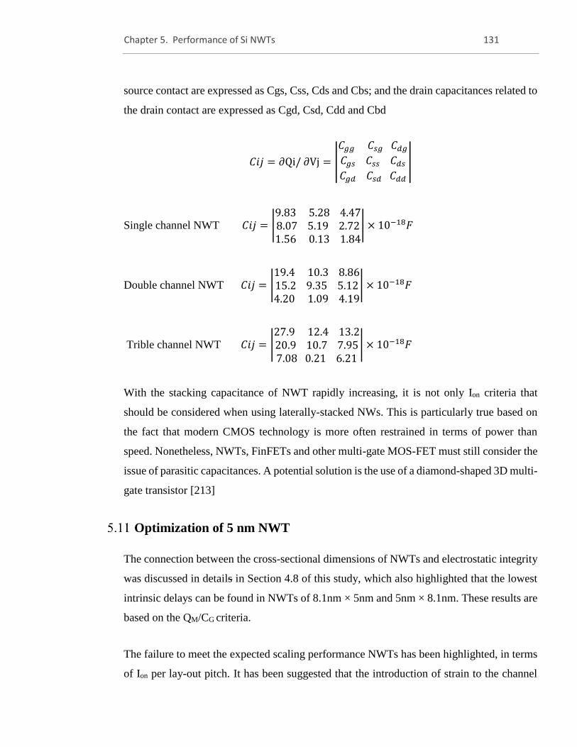
Chapter 5. Performance of Si NWTs 131
source contact are expressed as Cgs, Css, Cds and Cbs; and the drain capacitances related to
the drain contact are expressed as Cgd, Csd, Cdd and Cbd
𝐶𝑖𝑗 = ∂Qi/ ∂Vj = |
𝐶𝑔𝑔 𝐶𝑠𝑔 𝐶𝑑𝑔
𝐶𝑔𝑠 𝐶𝑠𝑠 𝐶𝑑𝑠
𝐶𝑔𝑑 𝐶𝑠𝑑 𝐶𝑑𝑑
|
Single channel NWT 𝐶𝑖𝑗 = |9.83 5.28 4.478.07 5.19 2.721.56 0.13 1.84
| × 10−18𝐹
Double channel NWT 𝐶𝑖𝑗 = |19.4 10.3 8.8615.2 9.35 5.124.20 1.09 4.19
| × 10−18𝐹
Trible channel NWT 𝐶𝑖𝑗 = |27.9 12.4 13.220.9 10.7 7.957.08 0.21 6.21
| × 10−18𝐹
With the stacking capacitance of NWT rapidly increasing, it is not only Ion criteria that
should be considered when using laterally-stacked NWs. This is particularly true based on
the fact that modern CMOS technology is more often restrained in terms of power than
speed. Nonetheless, NWTs, FinFETs and other multi-gate MOS-FET must still consider the
issue of parasitic capacitances. A potential solution is the use of a diamond-shaped 3D multi-
gate transistor [213]
Optimization of 5 nm NWT
The connection between the cross-sectional dimensions of NWTs and electrostatic integrity
was discussed in details in Section 4.8 of this study, which also highlighted that the lowest
intrinsic delays can be found in NWTs of 8.1nm × 5nm and 5nm × 8.1nm. These results are
based on the QM/CG criteria.
The failure to meet the expected scaling performance NWTs has been highlighted, in terms
of Ion per lay-out pitch. It has been suggested that the introduction of strain to the channel
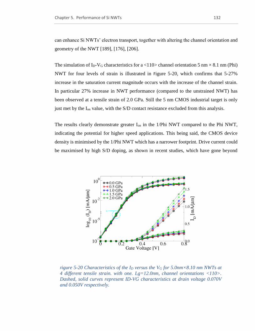
Chapter 5. Performance of Si NWTs 132
can enhance Si NWTs’ electron transport, together with altering the channel orientation and
geometry of the NWT [189], [176], [206].
The simulation of ID-VG characteristics for a <110> channel orientation 5 nm × 8.1 nm (Phi)
NWT for four levels of strain is illustrated in Figure 5-20, which confirms that 5-27%
increase in the saturation current magnitude occurs with the increase of the channel strain.
In particular 27% increase in NWT performance (compared to the unstrained NWT) has
been observed at a tensile strain of 2.0 GPa. Still the 5 nm CMOS industrial target is only
just met by the Ion value, with the S/D contact resistance excluded from this analysis.
The results clearly demonstrate greater Ion in the 1/Phi NWT compared to the Phi NWT,
indicating the potential for higher speed applications. This being said, the CMOS device
density is minimised by the 1/Phi NWT which has a narrower footprint. Drive current could
be maximised by high S/D doping, as shown in recent studies, which have gone beyond
Figure 5-20 Characteristics of the ID versus the VG for 5.0nm×8.10 nm NWTs at
4 different tensile strain. with one. Lg=12.0nm, channel orientations <110>.
Dashed, solid curves represent ID-VG characteristics at drain voltage 0.070V
and 0.050V respectively.
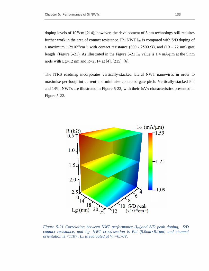
Chapter 5. Performance of Si NWTs 133
doping levels of 1021cm [214]; however, the development of 5 nm technology still requires
further work in the area of contact resistance. Phi NWT Ion is compared with S/D doping of
a maximum 1.2x1021cm-3, with contact resistance (500 - 2500 Ω), and (10 – 22 nm) gate
length (Figure 5-21). As illustrated in the Figure 5-21 Ion value is 1.4 mA/µm at the 5 nm
node with Lg=12 nm and R=2314 Ω [4], [215], [6].
The ITRS roadmap incorporates vertically-stacked lateral NWT nanowires in order to
maximise per-footprint current and minimise contacted gate pitch. Vertically-stacked Phi
and 1/Phi NWTs are illustrated in Figure 5-23, with their IDVG characteristics presented in
Figure 5-22.
Figure 5-21 Correlation between NWT performance (Ion)and S/D peak doping, S/D
contact resistance, and Lg. NWT cross-section is Phi (5.0nm×8.1nm) and channel
orientation is <110>. Ion is evaluated at VD=0.70V.
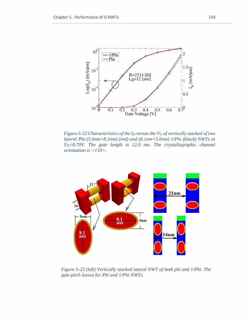
Chapter 5. Performance of Si NWTs 134
Figure 5-22 Characteristics of the ID versus the VG of vertically stacked of two
lateral Phi (5.0nm×8.1nm) (red) and (8.1nm×5.0nm) 1/Phi (black) NWTs at
VD=0.70V. The gate length is 12.0 nm. The crystallographic channel
orientation is <110>.
Figure 5-23 (left) Vertically stacked lateral NWT of both phi and 1/Phi. The
gate pitch layout for Phi and 1/Phi NWTs.
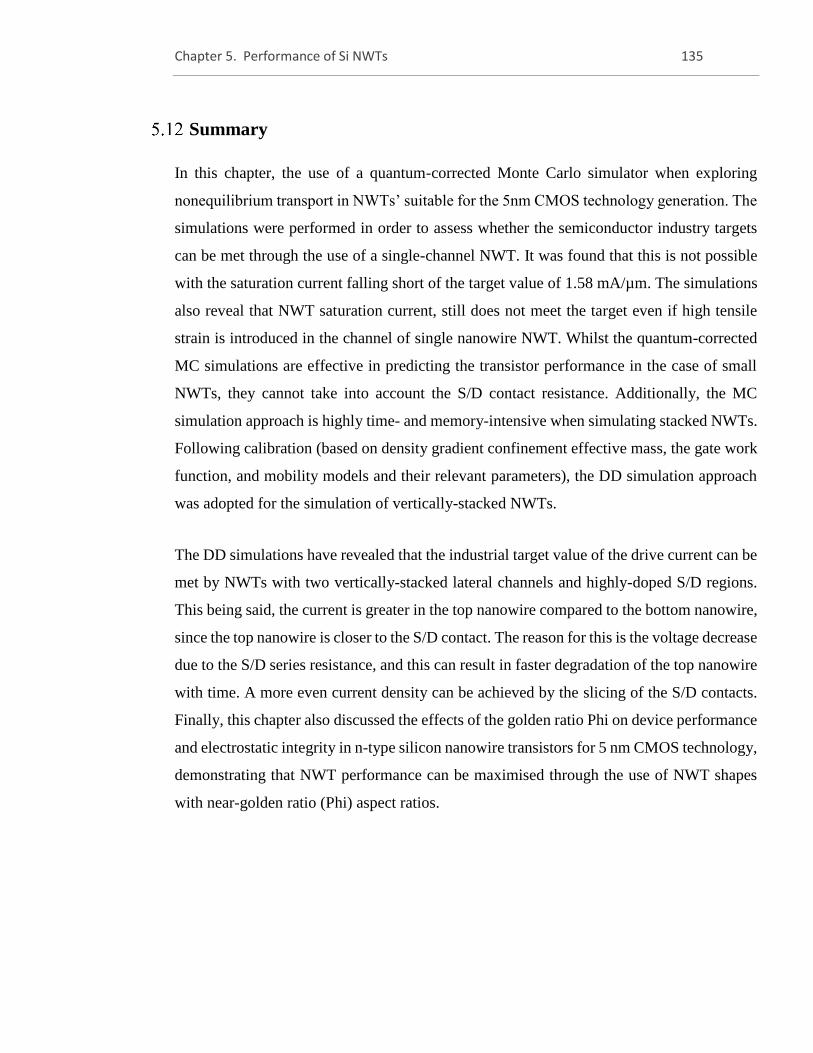
Chapter 5. Performance of Si NWTs 135
Summary
In this chapter, the use of a quantum-corrected Monte Carlo simulator when exploring
nonequilibrium transport in NWTs’ suitable for the 5nm CMOS technology generation. The
simulations were performed in order to assess whether the semiconductor industry targets
can be met through the use of a single-channel NWT. It was found that this is not possible
with the saturation current falling short of the target value of 1.58 mA/µm. The simulations
also reveal that NWT saturation current, still does not meet the target even if high tensile
strain is introduced in the channel of single nanowire NWT. Whilst the quantum-corrected
MC simulations are effective in predicting the transistor performance in the case of small
NWTs, they cannot take into account the S/D contact resistance. Additionally, the MC
simulation approach is highly time- and memory-intensive when simulating stacked NWTs.
Following calibration (based on density gradient confinement effective mass, the gate work
function, and mobility models and their relevant parameters), the DD simulation approach
was adopted for the simulation of vertically-stacked NWTs.
The DD simulations have revealed that the industrial target value of the drive current can be
met by NWTs with two vertically-stacked lateral channels and highly-doped S/D regions.
This being said, the current is greater in the top nanowire compared to the bottom nanowire,
since the top nanowire is closer to the S/D contact. The reason for this is the voltage decrease
due to the S/D series resistance, and this can result in faster degradation of the top nanowire
with time. A more even current density can be achieved by the slicing of the S/D contacts.
Finally, this chapter also discussed the effects of the golden ratio Phi on device performance
and electrostatic integrity in n-type silicon nanowire transistors for 5 nm CMOS technology,
demonstrating that NWT performance can be maximised through the use of NWT shapes
with near-golden ratio (Phi) aspect ratios.
Chapter 6. Study of statistical variability 136
6 Chapter 6. Study of statistical variability
Introduction
NWT statistical variability, associated with the discreteness of charge and granularity of
matter, which cannot be controlled through tightening process control and which is a key
contributor to variability in CMOS devices, is discussed in this chapter. It is possible to
model deterministically the impact of stress and lithography on the systematic CMOS
variability, and to capture this in the design and verification process. However, it is only
possible to model and represent the impact of the statistical variability on the transistor
characteristics probabilistically. When measuring a pair of identical adjacently-placed
transistors, the two transistors can have characteristics from the extreme tails of the statistical
distribution.
Today, the traditional approach of simulating, designing and describing CMOS transistors,
in terms of smooth interfaces and boundaries and continuous ionised dopant charge, is
becoming outdated. The contemporary transistors are increasingly atomistic in nature.
Figure 6-1illustrates the random discrete dopants (RDD) in a NWT with S/D peak doping
NS/D=1×1020cm-1 and NS/D=8×1020cm-1, and with channel doping Nch=1×1017cm-1. The top
of the image illustrates the random dopant distributions. The middle illustrates the impact of
RDD on the 3D electric potential distribution. The bottom of the image illustrates the impact
of RDD on the NWT’s potential distribution, depicted by the sliced y-x and z-x plane at the
centre of the two NWTs.
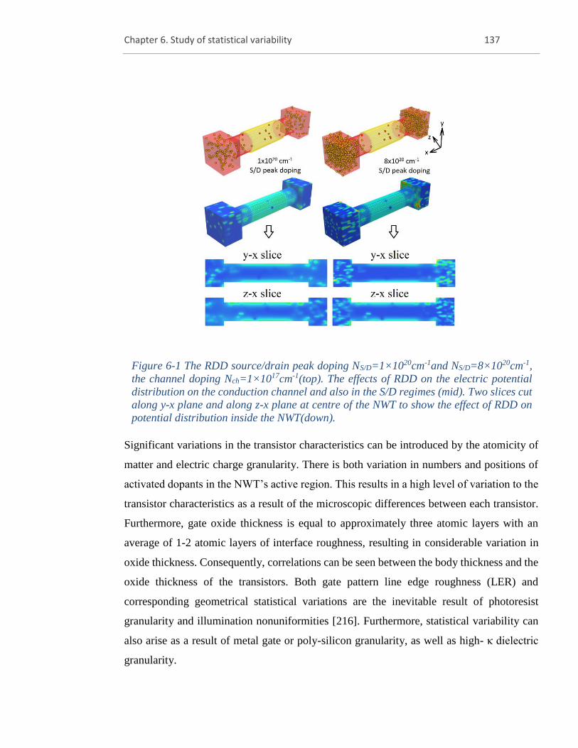
Chapter 6. Study of statistical variability 137
Significant variations in the transistor characteristics can be introduced by the atomicity of
matter and electric charge granularity. There is both variation in numbers and positions of
activated dopants in the NWT’s active region. This results in a high level of variation to the
transistor characteristics as a result of the microscopic differences between each transistor.
Furthermore, gate oxide thickness is equal to approximately three atomic layers with an
average of 1-2 atomic layers of interface roughness, resulting in considerable variation in
oxide thickness. Consequently, correlations can be seen between the body thickness and the
oxide thickness of the transistors. Both gate pattern line edge roughness (LER) and
corresponding geometrical statistical variations are the inevitable result of photoresist
granularity and illumination nonuniformities [216]. Furthermore, statistical variability can
also arise as a result of metal gate or poly-silicon granularity, as well as high- κ dielectric
granularity.
Figure 6-1 The RDD source/drain peak doping NS/D=1×1020cm-1and NS/D=8×1020cm-1,
the channel doping Nch=1×1017cm-1(top). The effects of RDD on the electric potential
distribution on the conduction channel and also in the S/D regimes (mid). Two slices cut
along y-x plane and along z-x plane at centre of the NWT to show the effect of RDD on
potential distribution inside the NWT(down).
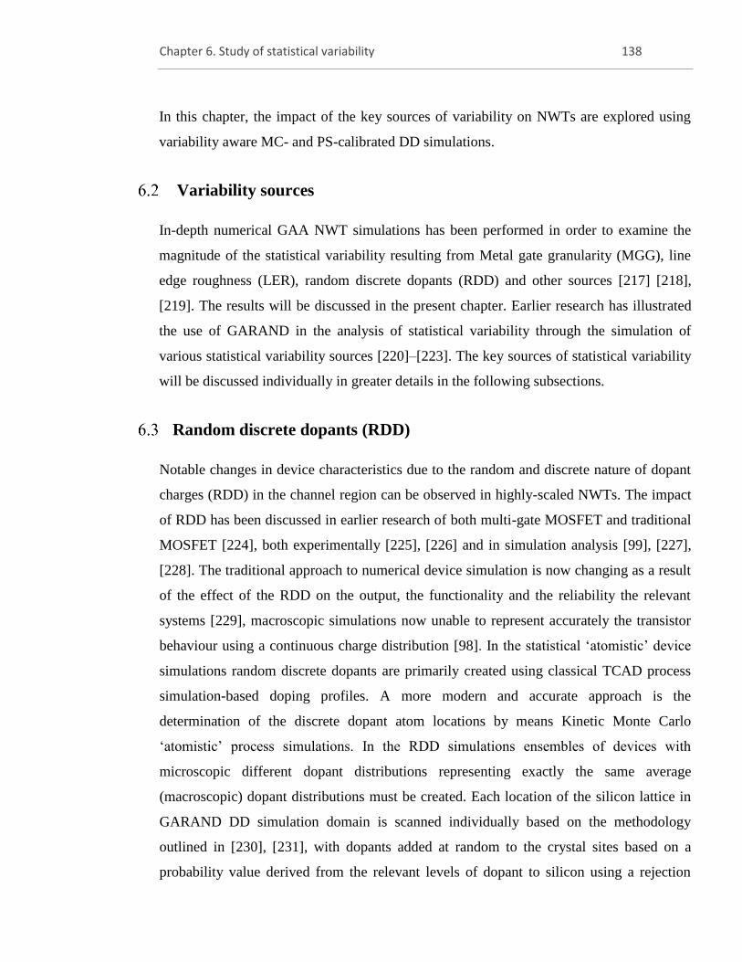
Chapter 6. Study of statistical variability 138
In this chapter, the impact of the key sources of variability on NWTs are explored using
variability aware MC- and PS-calibrated DD simulations.
Variability sources
In-depth numerical GAA NWT simulations has been performed in order to examine the
magnitude of the statistical variability resulting from Metal gate granularity (MGG), line
edge roughness (LER), random discrete dopants (RDD) and other sources [217] [218],
[219]. The results will be discussed in the present chapter. Earlier research has illustrated
the use of GARAND in the analysis of statistical variability through the simulation of
various statistical variability sources [220]–[223]. The key sources of statistical variability
will be discussed individually in greater details in the following subsections.
Random discrete dopants (RDD)
Notable changes in device characteristics due to the random and discrete nature of dopant
charges (RDD) in the channel region can be observed in highly-scaled NWTs. The impact
of RDD has been discussed in earlier research of both multi-gate MOSFET and traditional
MOSFET [224], both experimentally [225], [226] and in simulation analysis [99], [227],
[228]. The traditional approach to numerical device simulation is now changing as a result
of the effect of the RDD on the output, the functionality and the reliability the relevant
systems [229], macroscopic simulations now unable to represent accurately the transistor
behaviour using a continuous charge distribution [98]. In the statistical ‘atomistic’ device
simulations random discrete dopants are primarily created using classical TCAD process
simulation-based doping profiles. A more modern and accurate approach is the
determination of the discrete dopant atom locations by means Kinetic Monte Carlo
‘atomistic’ process simulations. In the RDD simulations ensembles of devices with
microscopic different dopant distributions representing exactly the same average
(macroscopic) dopant distributions must be created. Each location of the silicon lattice in
GARAND DD simulation domain is scanned individually based on the methodology
outlined in [230], [231], with dopants added at random to the crystal sites based on a
probability value derived from the relevant levels of dopant to silicon using a rejection
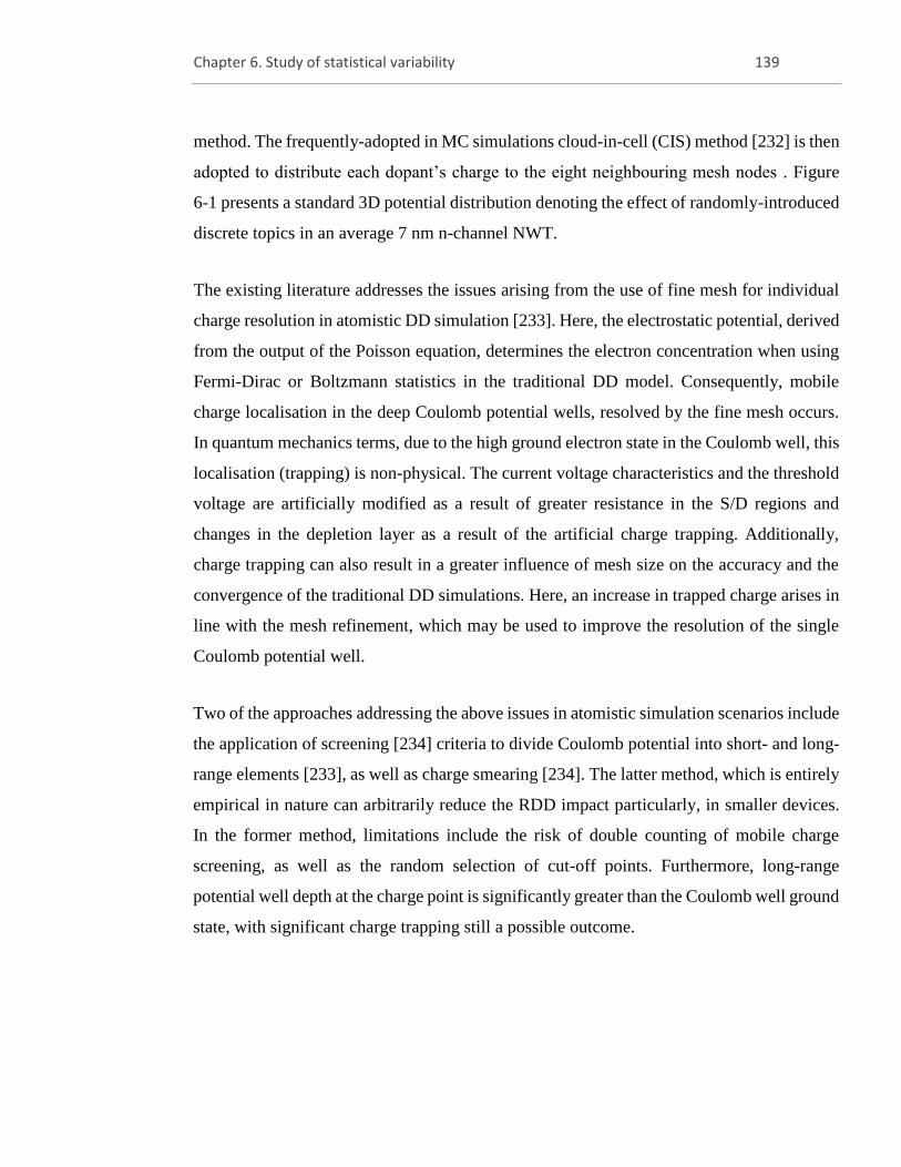
Chapter 6. Study of statistical variability 139
method. The frequently-adopted in MC simulations cloud-in-cell (CIS) method [232] is then
adopted to distribute each dopant’s charge to the eight neighbouring mesh nodes . Figure
6-1 presents a standard 3D potential distribution denoting the effect of randomly-introduced
discrete topics in an average 7 nm n-channel NWT.
The existing literature addresses the issues arising from the use of fine mesh for individual
charge resolution in atomistic DD simulation [233]. Here, the electrostatic potential, derived
from the output of the Poisson equation, determines the electron concentration when using
Fermi-Dirac or Boltzmann statistics in the traditional DD model. Consequently, mobile
charge localisation in the deep Coulomb potential wells, resolved by the fine mesh occurs.
In quantum mechanics terms, due to the high ground electron state in the Coulomb well, this
localisation (trapping) is non-physical. The current voltage characteristics and the threshold
voltage are artificially modified as a result of greater resistance in the S/D regions and
changes in the depletion layer as a result of the artificial charge trapping. Additionally,
charge trapping can also result in a greater influence of mesh size on the accuracy and the
convergence of the traditional DD simulations. Here, an increase in trapped charge arises in
line with the mesh refinement, which may be used to improve the resolution of the single
Coulomb potential well.
Two of the approaches addressing the above issues in atomistic simulation scenarios include
the application of screening [234] criteria to divide Coulomb potential into short- and long-
range elements [233], as well as charge smearing [234]. The latter method, which is entirely
empirical in nature can arbitrarily reduce the RDD impact particularly, in smaller devices.
In the former method, limitations include the risk of double counting of mobile charge
screening, as well as the random selection of cut-off points. Furthermore, long-range
potential well depth at the charge point is significantly greater than the Coulomb well ground
state, with significant charge trapping still a possible outcome.
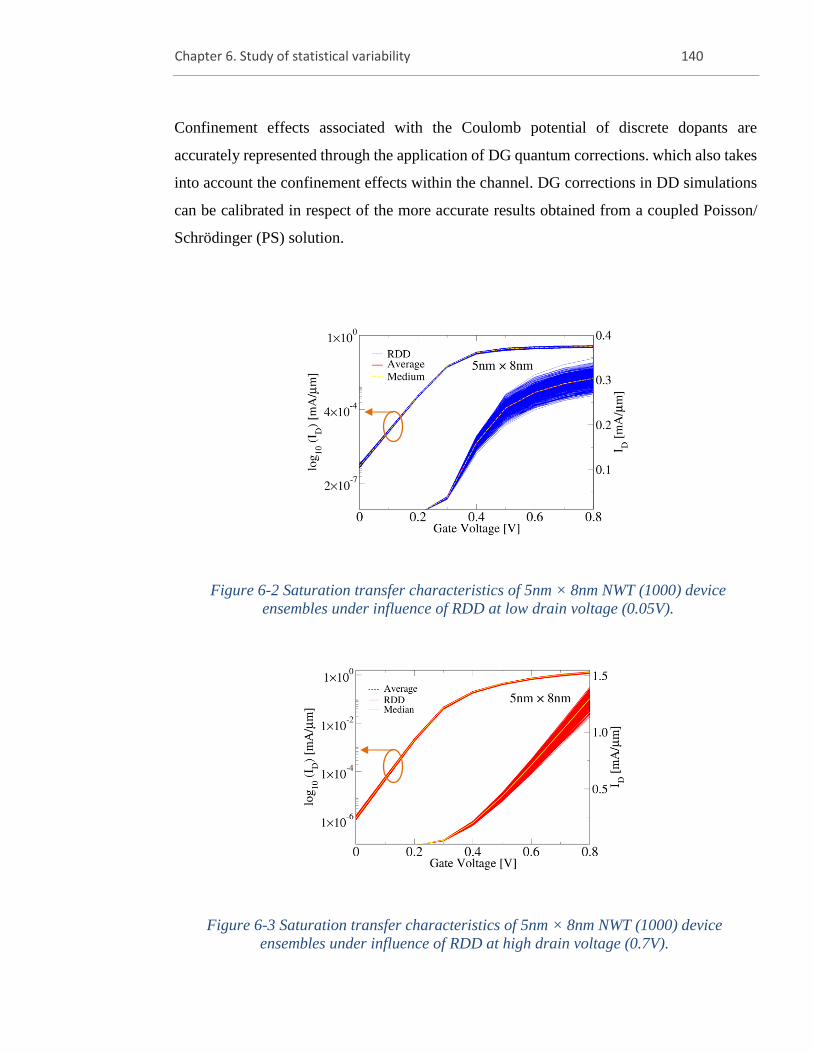
Chapter 6. Study of statistical variability 140
Confinement effects associated with the Coulomb potential of discrete dopants are
accurately represented through the application of DG quantum corrections. which also takes
into account the confinement effects within the channel. DG corrections in DD simulations
can be calibrated in respect of the more accurate results obtained from a coupled Poisson/
Schrödinger (PS) solution.
Figure 6-3 Saturation transfer characteristics of 5nm × 8nm NWT (1000) device
ensembles under influence of RDD at high drain voltage (0.7V).
Figure 6-2 Saturation transfer characteristics of 5nm × 8nm NWT (1000) device
ensembles under influence of RDD at low drain voltage (0.05V).
Chapter 6. Study of statistical variability 141
The microscopic effects of RDD within device 7 nm NWT are illustrated in Figure 6-1, with
RDD-based potential fluctuation also presented. Here, S/D peak doping is NS/D=1x1020cm-1
and NS/D=8x1020 cm-1, whilst channel doping is Nch=1x1017cm-1 (shown at the top of the
image). The figure also demonstrates the impact of RDD on electric potential distribution in
the conduction channel and S/D regimes. The impact of RDD on the potential distribution
within the NWT is illustrated in the y-x and z-x slices through the NWT centre. The S/D
regimes demonstrate significant fluctuation in electric potential, with the S/D extensions
showing a lower level of fluctuation. The doping concentrate has an influence on the
different levels of potential fluctuation seen in these simulations. Because there are a small
number of ionised acceptors in the gate region of the Si channel, this results in smooth
potential within the channel. It is interesting to note that because of the low doping in the
channel, RDD VT fluctuations are minimised in NWTs compared to conventional
MOSFETS.
This section discusses the effect of RDD on the on current Ion and the threshold voltage VT
in NWT with two cross sections of 5 nm and equal gate lengths. The RDD-based fluctuations
are simulated using a statistical ensemble of 1,000 microscopically different NWTs.
Significant fluctuations in S/D access resistance arise as a result of the potential fluctuation
stemming from S/D extension donors, leading to greater on-current variance. RDD
introduces also VT fluctuations as a result the potential fluctuations in the channel. Figure
6-3 depicts the set of 1,000 gate transfer characteristics at high drain voltage, while Figure
6-2 depicting the low drain voltage characteristics. There is a relatively low I-V dispersion
in the sub-threshold region due to the relatively low-doped channel, with a rapid increase in
on-current dispersion occurring as performed result of the access resistance variation which
has greater impact at low drain bias.
Figure 6-4 and Figure 6-5 respectively illustrate the correlation between the on-current and
the threshold voltage at high and low drain bias. The standard deviation of the threshold
voltage (σVT) at high and low drain biases is 1.99 mV and 1.48 mV respectively. These low
standard deviations suggest that VT fluctuations are effectively minimised due to the low
channel doping, with no ionised impurities beneath the gate in most cases. At the high drain
voltage, the on-current standard deviation (σIon) is 0.0412 mA/μm, with the low drain
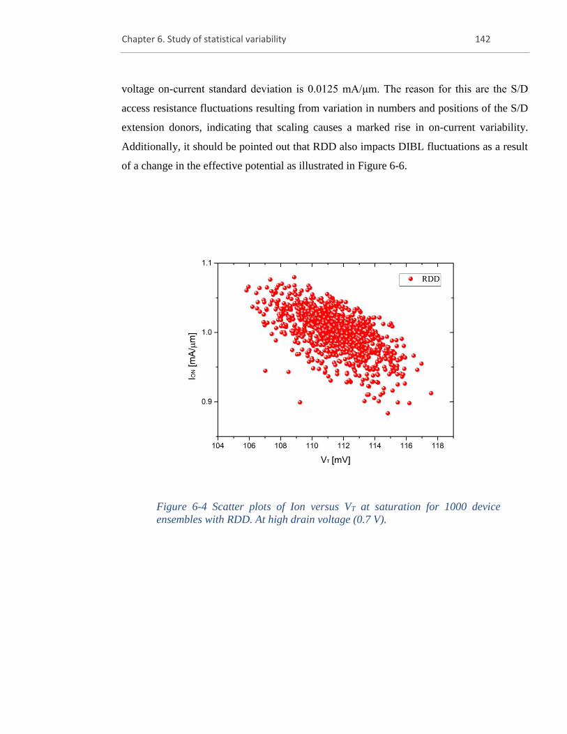
Chapter 6. Study of statistical variability 142
voltage on-current standard deviation is 0.0125 mA/μm. The reason for this are the S/D
access resistance fluctuations resulting from variation in numbers and positions of the S/D
extension donors, indicating that scaling causes a marked rise in on-current variability.
Additionally, it should be pointed out that RDD also impacts DIBL fluctuations as a result
of a change in the effective potential as illustrated in Figure 6-6.
Figure 6-4 Scatter plots of Ion versus VT at saturation for 1000 device
ensembles with RDD. At high drain voltage (0.7 V).
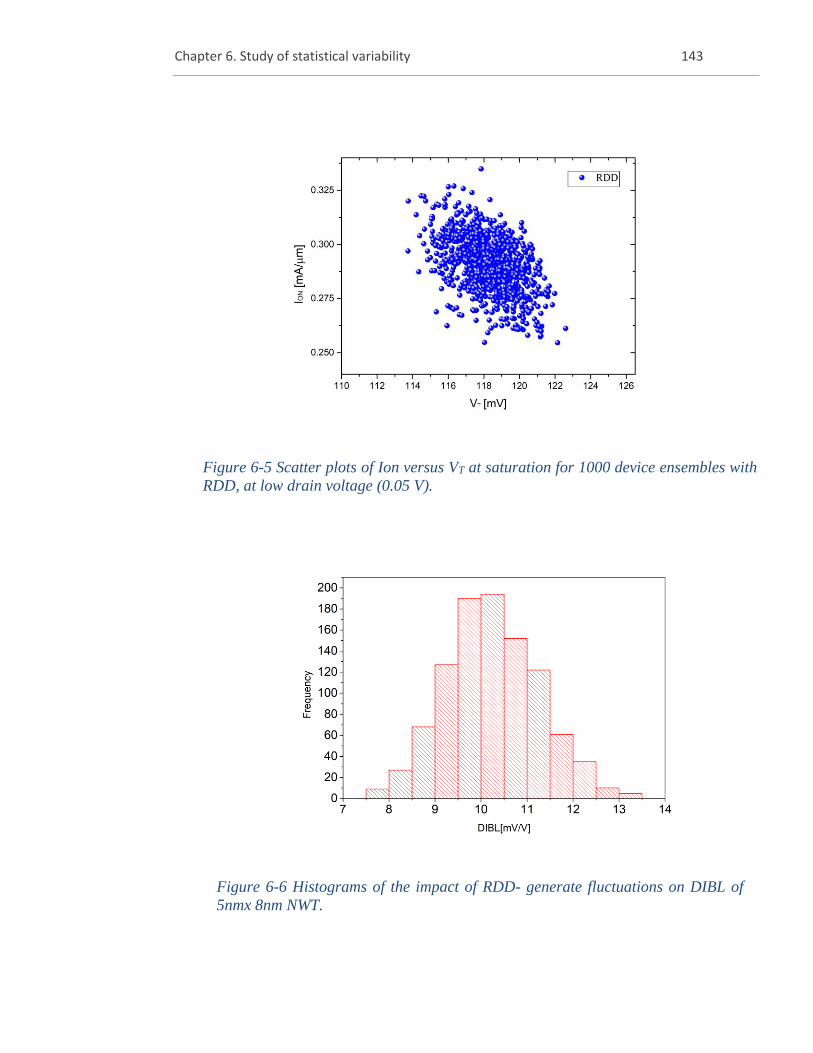
Chapter 6. Study of statistical variability 143
Figure 6-5 Scatter plots of Ion versus VT at saturation for 1000 device ensembles with
RDD, at low drain voltage (0.05 V).
Figure 6-6 Histograms of the impact of RDD- generate fluctuations on DIBL of
5nmx 8nm NWT.
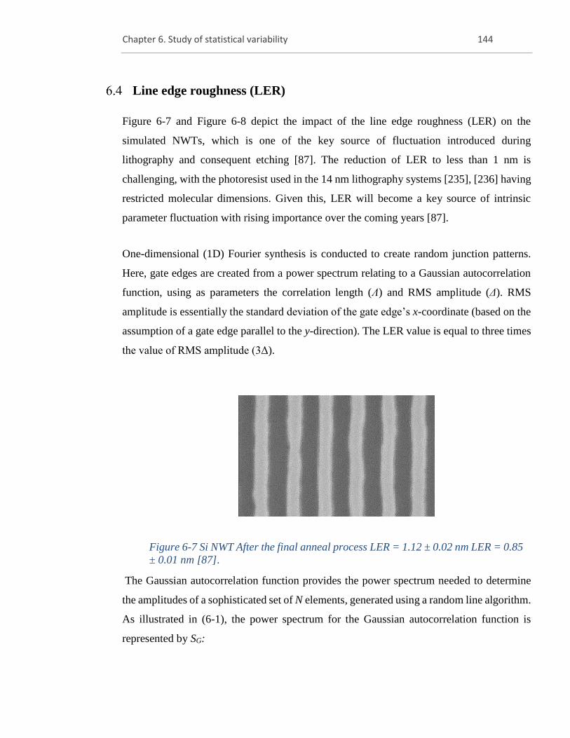
Chapter 6. Study of statistical variability 144
Line edge roughness (LER)
Figure 6-7 and Figure 6-8 depict the impact of the line edge roughness (LER) on the
simulated NWTs, which is one of the key source of fluctuation introduced during
lithography and consequent etching [87]. The reduction of LER to less than 1 nm is
challenging, with the photoresist used in the 14 nm lithography systems [235], [236] having
restricted molecular dimensions. Given this, LER will become a key source of intrinsic
parameter fluctuation with rising importance over the coming years [87].
One-dimensional (1D) Fourier synthesis is conducted to create random junction patterns.
Here, gate edges are created from a power spectrum relating to a Gaussian autocorrelation
function, using as parameters the correlation length (Ʌ) and RMS amplitude (Δ). RMS
amplitude is essentially the standard deviation of the gate edge’s x-coordinate (based on the
assumption of a gate edge parallel to the y-direction). The LER value is equal to three times
the value of RMS amplitude (3Δ).
The Gaussian autocorrelation function provides the power spectrum needed to determine
the amplitudes of a sophisticated set of N elements, generated using a random line algorithm.
As illustrated in (6-1), the power spectrum for the Gaussian autocorrelation function is
represented by SG:
Figure 6-7 Si NWT After the final anneal process LER = 1.12 ± 0.02 nm LER = 0.85
± 0.01 nm [87].
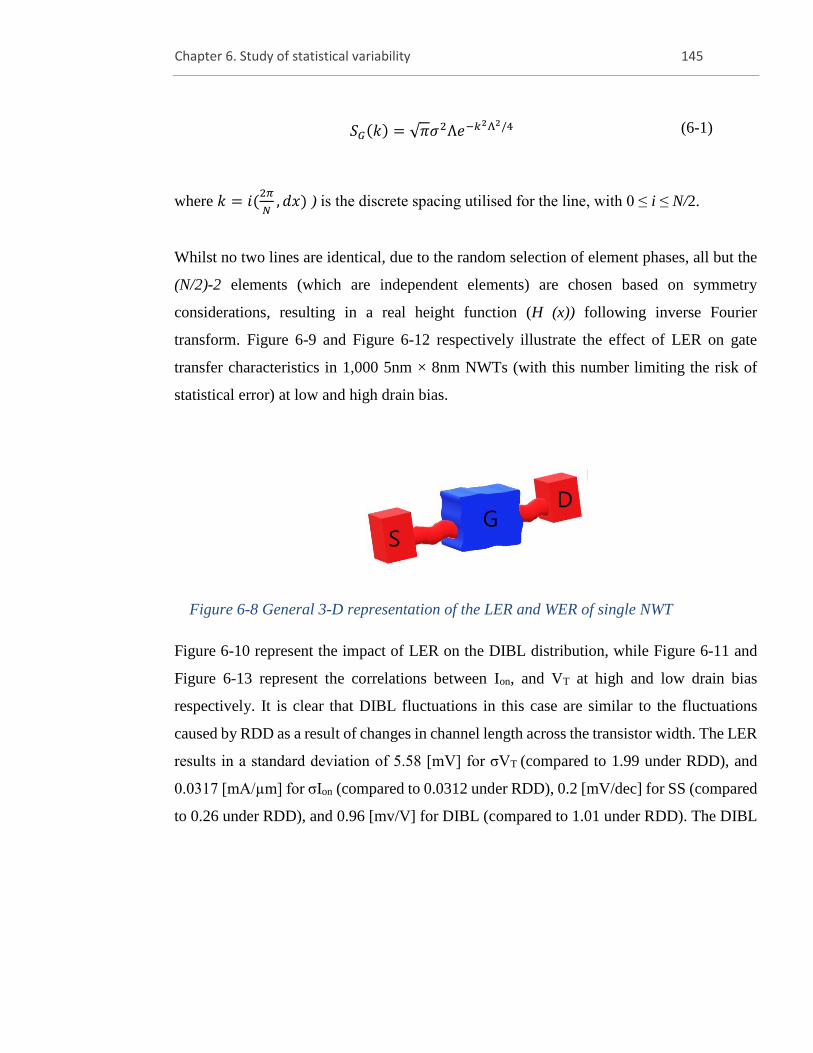
Chapter 6. Study of statistical variability 145
𝑆𝐺(𝑘) = √𝜋𝜎2Λ𝑒−𝑘2Λ2/4 (6-1)
where 𝑘 = 𝑖(2𝜋
𝑁, 𝑑𝑥) ) is the discrete spacing utilised for the line, with 0 ≤ i ≤ N/2.
Whilst no two lines are identical, due to the random selection of element phases, all but the
(N/2)-2 elements (which are independent elements) are chosen based on symmetry
considerations, resulting in a real height function (H (x)) following inverse Fourier
transform. Figure 6-9 and Figure 6-12 respectively illustrate the effect of LER on gate
transfer characteristics in 1,000 5nm × 8nm NWTs (with this number limiting the risk of
statistical error) at low and high drain bias.
Figure 6-10 represent the impact of LER on the DIBL distribution, while Figure 6-11 and
Figure 6-13 represent the correlations between Ion, and VT at high and low drain bias
respectively. It is clear that DIBL fluctuations in this case are similar to the fluctuations
caused by RDD as a result of changes in channel length across the transistor width. The LER
results in a standard deviation of 5.58 [mV] for σVT (compared to 1.99 under RDD), and
0.0317 [mA/µm] for σIon (compared to 0.0312 under RDD), 0.2 [mV/dec] for SS (compared
to 0.26 under RDD), and 0.96 [mv/V] for DIBL (compared to 1.01 under RDD). The DIBL
Figure 6-8 General 3-D representation of the LER and WER of single NWT
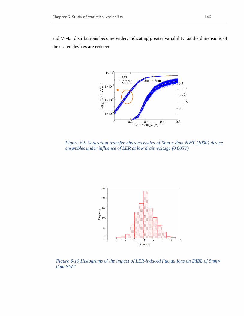
Chapter 6. Study of statistical variability 146
and VT-Ion distributions become wider, indicating greater variability, as the dimensions of
the scaled devices are reduced
Figure 6-9 Saturation transfer characteristics of 5nm x 8nm NWT (1000) device
ensembles under influence of LER at low drain voltage (0.005V)
Figure 6-10 Histograms of the impact of LER-induced fluctuations on DIBL of 5nm×
8nm NWT
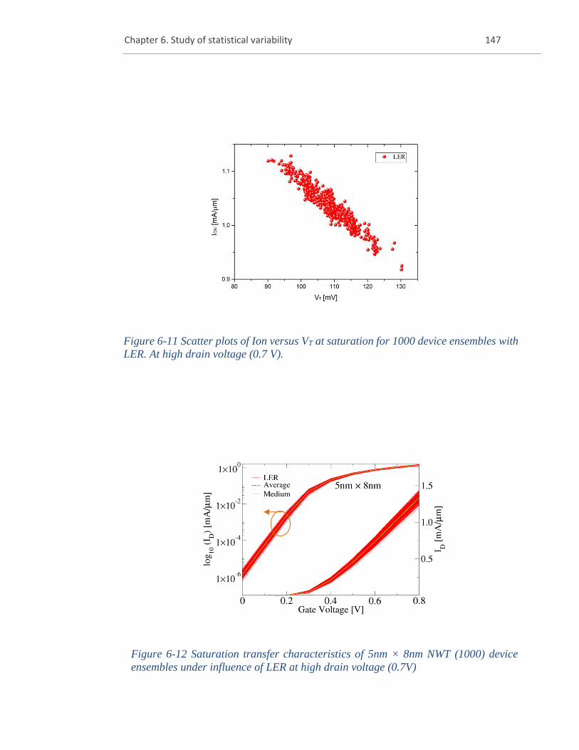
Chapter 6. Study of statistical variability 147
Figure 6-12 Saturation transfer characteristics of 5nm × 8nm NWT (1000) device
ensembles under influence of LER at high drain voltage (0.7V)
Figure 6-11 Scatter plots of Ion versus VT at saturation for 1000 device ensembles with
LER. At high drain voltage (0.7 V).
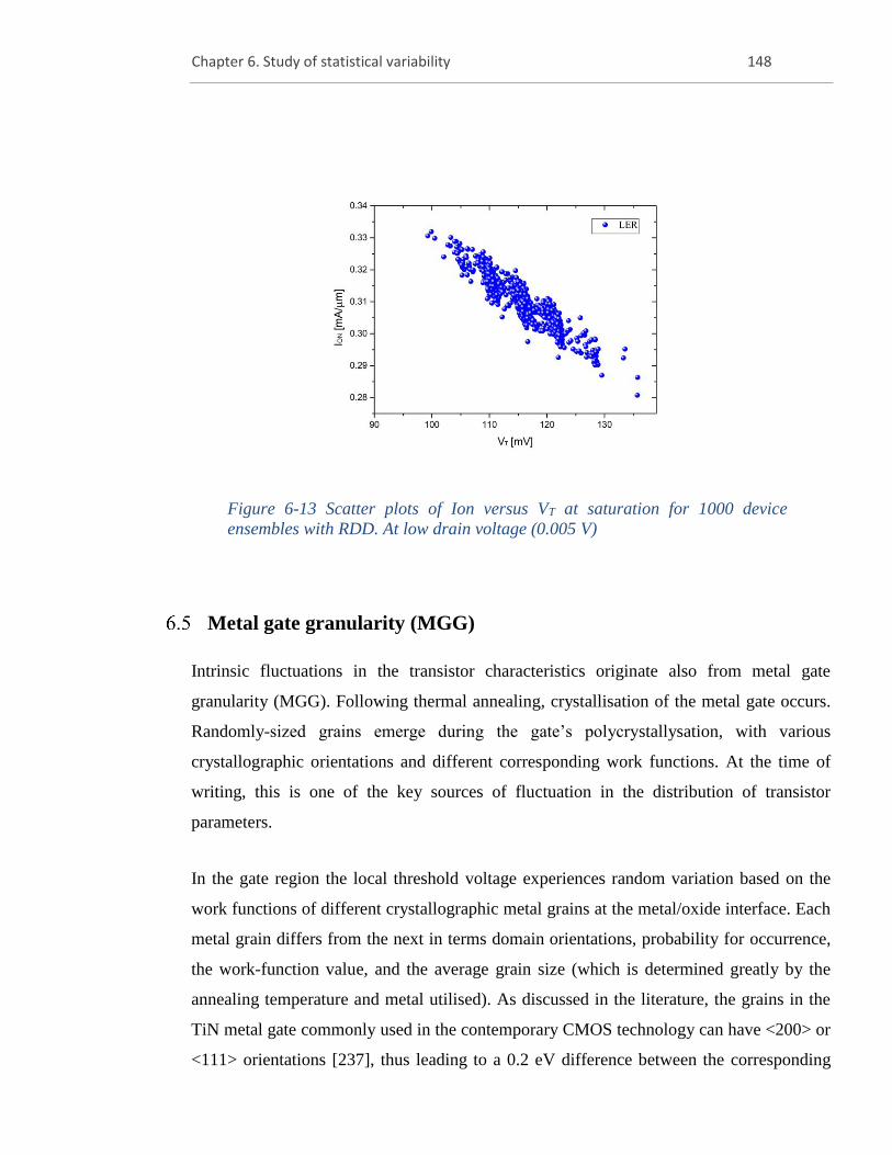
Chapter 6. Study of statistical variability 148
Metal gate granularity (MGG)
Intrinsic fluctuations in the transistor characteristics originate also from metal gate
granularity (MGG). Following thermal annealing, crystallisation of the metal gate occurs.
Randomly-sized grains emerge during the gate’s polycrystallysation, with various
crystallographic orientations and different corresponding work functions. At the time of
writing, this is one of the key sources of fluctuation in the distribution of transistor
parameters.
In the gate region the local threshold voltage experiences random variation based on the
work functions of different crystallographic metal grains at the metal/oxide interface. Each
metal grain differs from the next in terms domain orientations, probability for occurrence,
the work-function value, and the average grain size (which is determined greatly by the
annealing temperature and metal utilised). As discussed in the literature, the grains in the
TiN metal gate commonly used in the contemporary CMOS technology can have <200> or
<111> orientations [237], thus leading to a 0.2 eV difference between the corresponding
Figure 6-13 Scatter plots of Ion versus VT at saturation for 1000 device
ensembles with RDD. At low drain voltage (0.005 V)
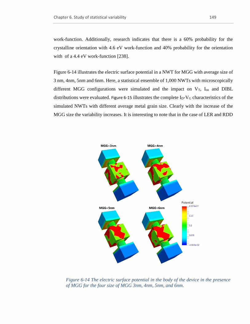
Chapter 6. Study of statistical variability 149
work-function. Additionally, research indicates that there is a 60% probability for the
crystalline orientation with 4.6 eV work-function and 40% probability for the orientation
with of a 4.4 eV work-function [238].
Figure 6-14 illustrates the electric surface potential in a NWT for MGG with average size of
3 nm, 4nm, 5nm and 6nm. Here, a statistical ensemble of 1,000 NWTs with microscopically
different MGG configurations were simulated and the impact on VT, Ion and DIBL
distributions were evaluated. Figure 6-15 illustrates the complete ID-VG characteristics of the
simulated NWTs with different average metal grain size. Clearly with the increase of the
MGG size the variability increases. It is interesting to note that in the case of LER and RDD
Figure 6-14 The electric surface potential in the body of the device in the presence
of MGG for the four size of MGG 3nm, 4nm, 5nm, and 6nm.
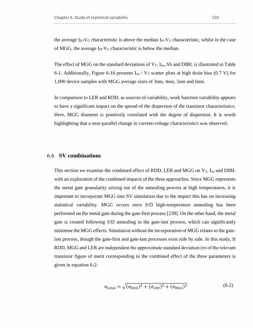
Chapter 6. Study of statistical variability 150
the average ID-VG characteristic is above the median ID-VG characteristic, whilst in the case
of MGG, the average ID-VG characteristic is below the median.
The effect of MGG on the standard deviations of VT, Ion, SS and DIBL is illustrated in Table
6-1. Additionally, Figure 6-16 presents Ion / VT scatter plots at high drain bias (0.7 V) for
1,000 device samples with MGG average sizes of 3nm, 4nm, 5nm and 6nm.
In comparison to LER and RDD, as sources of variability, work function variability appears
to have a significant impact on the spread of the dispersion of the transistor characteristics.
Here, MGG diameter is positively correlated with the degree of dispersion. It is worth
highlighting that a near-parallel change in current-voltage characteristics was observed.
SV combinations
This section we examine the combined effect of RDD, LER and MGG on VT, Ion and DIBL
with an exploration of the combined impacts of the three approaches. Since MGG represents
the metal gate granularity arising out of the annealing process at high temperatures, it is
important to incorporate MGG into SV simulation due to the impact this has on increasing
statistical variability. MGG occurs once S/D high-temperature annealing has been
performed on the metal gate during the gate-first process [239]. On the other hand, the metal
gate is created following S/D annealing in the gate-last process, which can significantly
minimise the MGG effects. Simulation without the incorporation of MGG relates to the gate-
last process, though the gate-first and gate-last processes exist side by side. In this study, If
RDD, MGG and LER are independent the approximate standard deviation (σ) of the relevant
transistor figure of merit corresponding to the combined effect of the three parameters is
given in equation 6-2:
𝜎𝑡𝑜𝑡𝑎𝑙 = √(𝜎𝑅𝐷𝐷)2 + (𝜎𝐿𝐸𝑅)2 + (𝜎𝑀𝐺𝐺)2 (6-2)
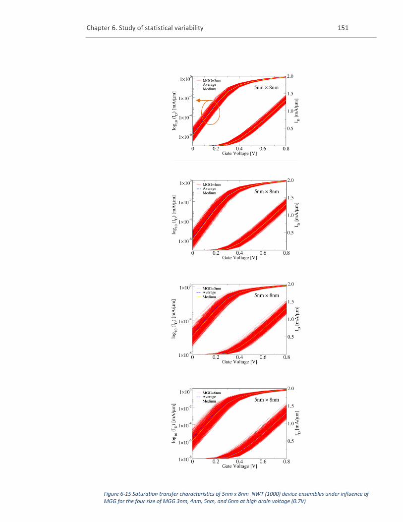
Chapter 6. Study of statistical variability 151
Figure 6-15 Saturation transfer characteristics of 5nm x 8nm NWT (1000) device ensembles under influence of MGG for the four size of MGG 3nm, 4nm, 5nm, and 6nm at high drain voltage (0.7V)
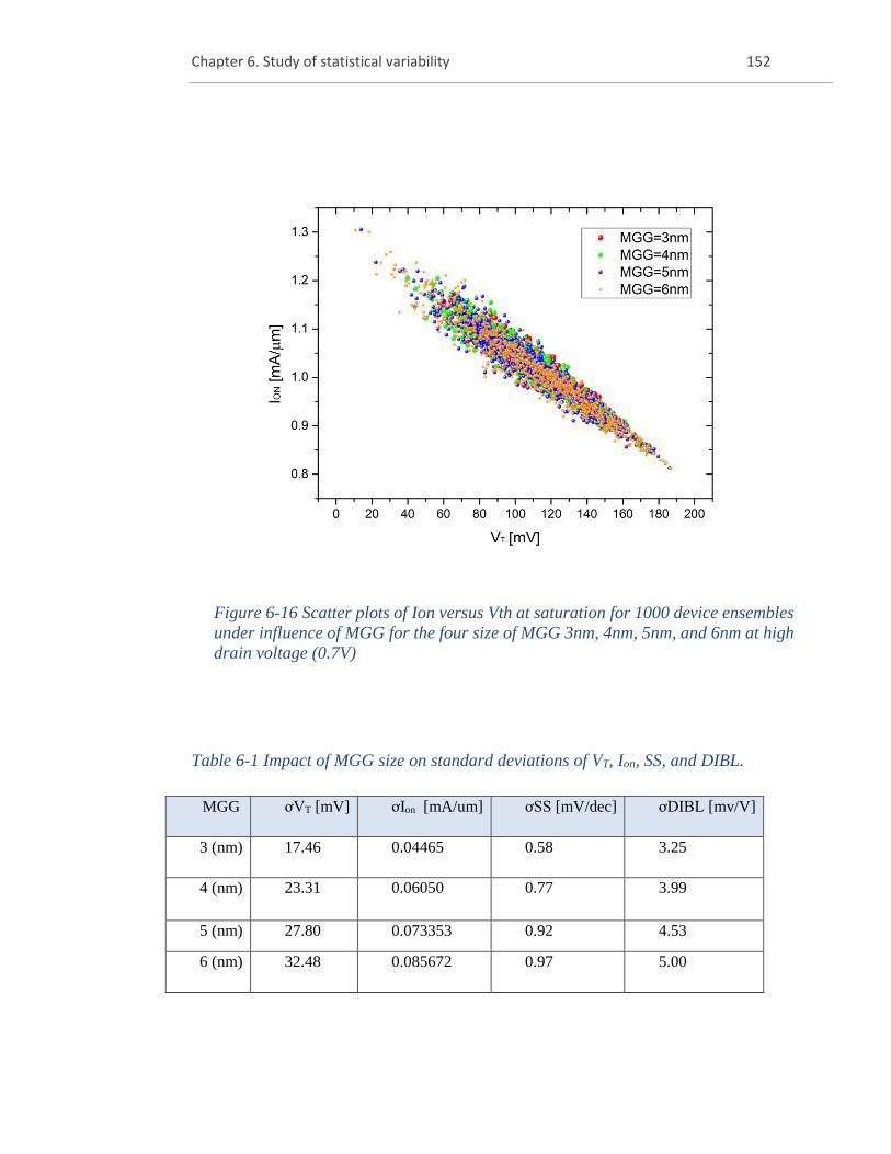
Chapter 6. Study of statistical variability 152
Table 6-1 Impact of MGG size on standard deviations of VT, Ion, SS, and DIBL.
MGG ơVT [mV] ơIon [mA/um] ơSS [mV/dec] ơDIBL [mv/V]
3 (nm) 17.46 0.04465 0.58 3.25
4 (nm) 23.31 0.06050 0.77 3.99
5 (nm) 27.80 0.073353 0.92 4.53
6 (nm) 32.48 0.085672 0.97 5.00
Figure 6-16 Scatter plots of Ion versus Vth at saturation for 1000 device ensembles
under influence of MGG for the four size of MGG 3nm, 4nm, 5nm, and 6nm at high
drain voltage (0.7V)
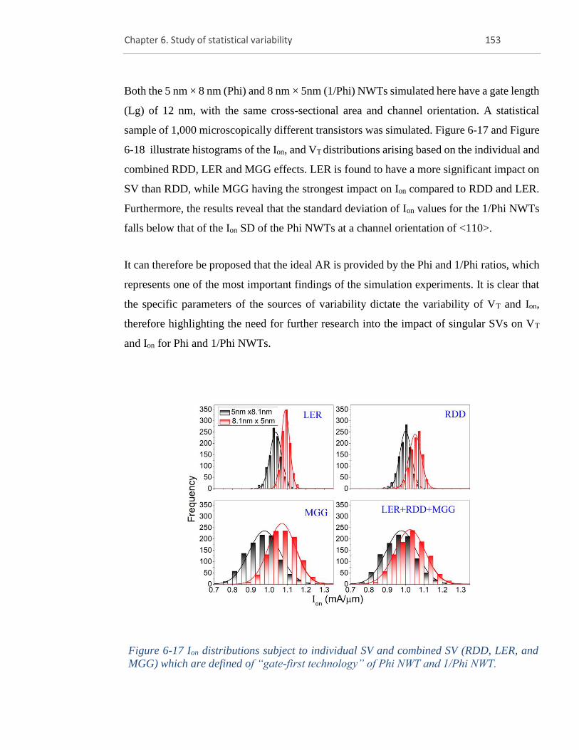
Chapter 6. Study of statistical variability 153
Both the 5 nm × 8 nm (Phi) and 8 nm × 5nm (1/Phi) NWTs simulated here have a gate length
(Lg) of 12 nm, with the same cross-sectional area and channel orientation. A statistical
sample of 1,000 microscopically different transistors was simulated. Figure 6-17 and Figure
6-18 illustrate histograms of the Ion, and VT distributions arising based on the individual and
combined RDD, LER and MGG effects. LER is found to have a more significant impact on
SV than RDD, while MGG having the strongest impact on Ion compared to RDD and LER.
Furthermore, the results reveal that the standard deviation of Ion values for the 1/Phi NWTs
falls below that of the Ion SD of the Phi NWTs at a channel orientation of <110>.
It can therefore be proposed that the ideal AR is provided by the Phi and 1/Phi ratios, which
represents one of the most important findings of the simulation experiments. It is clear that
the specific parameters of the sources of variability dictate the variability of VT and Ion,
therefore highlighting the need for further research into the impact of singular SVs on VT
and Ion for Phi and 1/Phi NWTs.
Figure 6-17 Ion distributions subject to individual SV and combined SV (RDD, LER, and
MGG) which are defined of “gate-first technology” of Phi NWT and 1/Phi NWT.
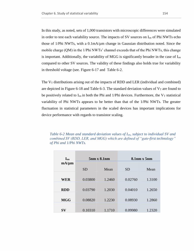
Chapter 6. Study of statistical variability 154
In this study, as noted, sets of 1,000 transistors with microscopic differences were simulated
in order to test each variability source. The impacts of SV sources on Ion of Phi NWTs echo
those of 1/Phi NWTs, with a 0.1mA/µm change in Gaussian distribution noted. Since the
mobile charge (QM) in the 1/Phi NWTs’ channel exceeds that of the Phi NWTs, this change
is important. Additionally, the variability of MGG is significantly broader in the case of Ion
compared to other SV sources. The validity of these findings also holds true for variability
in threshold voltage (see. Figure 6-17 and Table 6-2.
The VT distributions arising out of the impacts of RDD and LER (individual and combined)
are depicted in Figure 6-18 and Table 6-3. The standard deviation values of VT are found to
be positively related to Ion in both the Phi and 1/Phi devices. Furthermore, the VT statistical
variability of Phi NWTs appears to be better than that of the 1/Phi NWTs. The greater
fluctuation in statistical parameters in the scaled devices has important implications for
device performance with regards to transistor scaling.
Table 6-2 Mean and standard deviation values of Ion, subject to individual SV and
combined SV (RDD, LER, and MGG) which are defined of “gate-first technology”
of Phi and 1/Phi NWTs.
Ion
mA/µm
5nm x 8.1nm 8.1nm x 5nm
SD Mean SD Mean
WER 0.03800 1.2460 0.02760 1.3100
RDD 0.03790 1.2030 0.04010 1.2650
MGG 0.08820 1.2230 0.08930 1.2860
SV 0.10310 1.1710 0.09980 1.2320
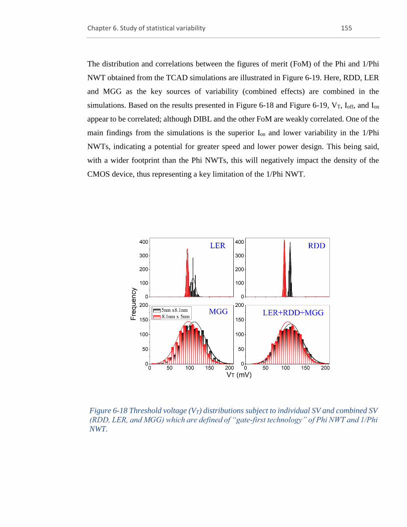
Chapter 6. Study of statistical variability 155
The distribution and correlations between the figures of merit (FoM) of the Phi and 1/Phi
NWT obtained from the TCAD simulations are illustrated in Figure 6-19. Here, RDD, LER
and MGG as the key sources of variability (combined effects) are combined in the
simulations. Based on the results presented in Figure 6-18 and Figure 6-19, VT, Ioff, and Ion
appear to be correlated; although DIBL and the other FoM are weakly correlated. One of the
main findings from the simulations is the superior Ion and lower variability in the 1/Phi
NWTs, indicating a potential for greater speed and lower power design. This being said,
with a wider footprint than the Phi NWTs, this will negatively impact the density of the
CMOS device, thus representing a key limitation of the 1/Phi NWT.
Figure 6-18 Threshold voltage (VT) distributions subject to individual SV and combined SV
(RDD, LER, and MGG) which are defined of “gate-first technology” of Phi NWT and 1/Phi
NWT.
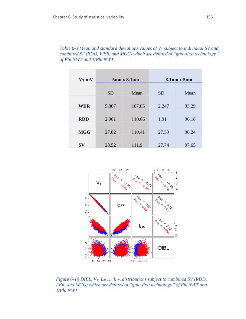
Chapter 6. Study of statistical variability 156
Figure 6-19 DIBL, VT, Ioff, and ION, distributions subject to combined SV (RDD,
LER, and MGG) which are defined of “gate-first technology” of Phi NWT and
1/Phi NWT
Table 6-3 Mean and standard deviations values of VT subject to individual SV and
combined SV (RDD, WER, and MGG) which are defined of “gate-first technology”
of Phi NWT and 1/Phi NWT.
VT mV 5nm x 8.1nm 8.1nm x 5nm
SD Mean SD Mean
WER 5.807 107.85 2.247 93.29
RDD 2.001 110.66 1.91 96.18
MGG 27.82 110.41 27.59 96.24
SV 28.52 111.9 27.74 97.65
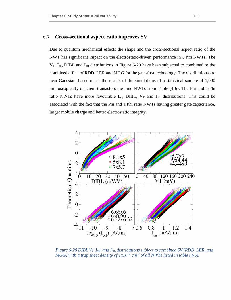
Chapter 6. Study of statistical variability 157
Cross-sectional aspect ratio improves SV
Due to quantum mechanical effects the shape and the cross-sectional aspect ratio of the
NWT has significant impact on the electrostatic-driven performance in 5 nm NWTs. The
VT, Ion, DIBL and Ioff distributions in Figure 6-20 have been subjected to combined to the
combined effect of RDD, LER and MGG for the gate-first technology. The distributions are
near-Gaussian, based on of the results of the simulations of a statistical sample of 1,000
microscopically different transistors the nine NWTs from Table (4-6). The Phi and 1/Phi
ratio NWTs have more favourable Ion, DIBL, VT and Ioff distributions. This could be
associated with the fact that the Phi and 1/Phi ratio NWTs having greater gate capacitance,
larger mobile charge and better electrostatic integrity.
Figure 6-20 DIBL VT, Ioff, and Ion, distributions subject to combined SV (RDD, LER, and
MGG) with a trap sheet density of 1x1012 cm-2 of all NWTs listed in table (4-6).
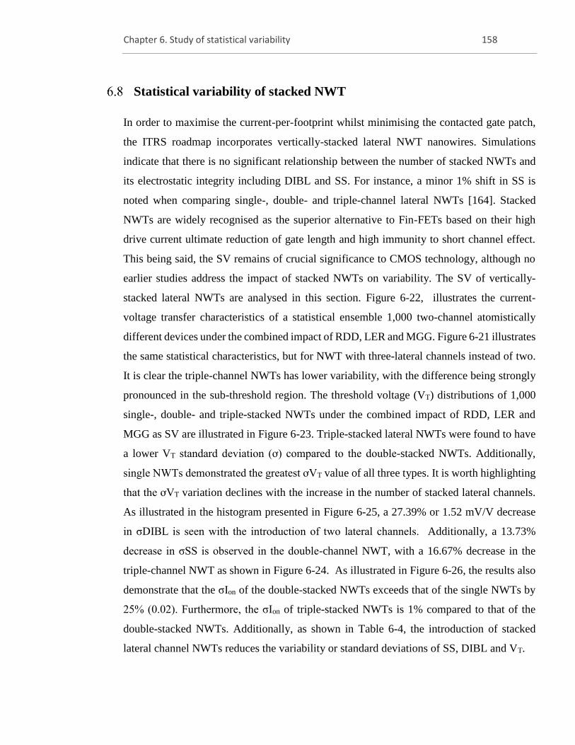
Chapter 6. Study of statistical variability 158
Statistical variability of stacked NWT
In order to maximise the current-per-footprint whilst minimising the contacted gate patch,
the ITRS roadmap incorporates vertically-stacked lateral NWT nanowires. Simulations
indicate that there is no significant relationship between the number of stacked NWTs and
its electrostatic integrity including DIBL and SS. For instance, a minor 1% shift in SS is
noted when comparing single-, double- and triple-channel lateral NWTs [164]. Stacked
NWTs are widely recognised as the superior alternative to Fin-FETs based on their high
drive current ultimate reduction of gate length and high immunity to short channel effect.
This being said, the SV remains of crucial significance to CMOS technology, although no
earlier studies address the impact of stacked NWTs on variability. The SV of vertically-
stacked lateral NWTs are analysed in this section. Figure 6-22, illustrates the current-
voltage transfer characteristics of a statistical ensemble 1,000 two-channel atomistically
different devices under the combined impact of RDD, LER and MGG. Figure 6-21 illustrates
the same statistical characteristics, but for NWT with three-lateral channels instead of two.
It is clear the triple-channel NWTs has lower variability, with the difference being strongly
pronounced in the sub-threshold region. The threshold voltage (VT) distributions of 1,000
single-, double- and triple-stacked NWTs under the combined impact of RDD, LER and
MGG as SV are illustrated in Figure 6-23. Triple-stacked lateral NWTs were found to have
a lower VT standard deviation (ơ) compared to the double-stacked NWTs. Additionally,
single NWTs demonstrated the greatest ơVT value of all three types. It is worth highlighting
that the ơVT variation declines with the increase in the number of stacked lateral channels.
As illustrated in the histogram presented in Figure 6-25, a 27.39% or 1.52 mV/V decrease
in σDIBL is seen with the introduction of two lateral channels. Additionally, a 13.73%
decrease in σSS is observed in the double-channel NWT, with a 16.67% decrease in the
triple-channel NWT as shown in Figure 6-24. As illustrated in Figure 6-26, the results also
demonstrate that the σIon of the double-stacked NWTs exceeds that of the single NWTs by
25% (0.02). Furthermore, the σIon of triple-stacked NWTs is 1% compared to that of the
double-stacked NWTs. Additionally, as shown in Table 6-4, the introduction of stacked
lateral channel NWTs reduces the variability or standard deviations of SS, DIBL and VT.
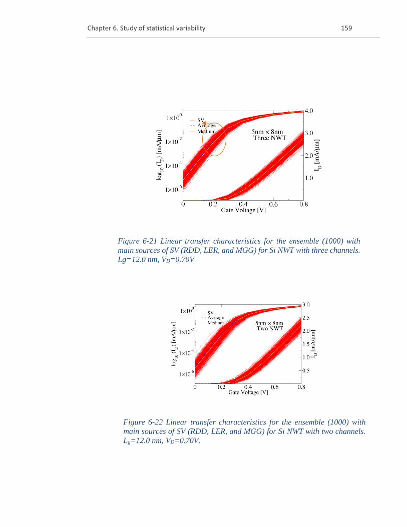
Chapter 6. Study of statistical variability 159
Figure 6-22 Linear transfer characteristics for the ensemble (1000) with
main sources of SV (RDD, LER, and MGG) for Si NWT with two channels.
Lg=12.0 nm, VD=0.70V.
Figure 6-21 Linear transfer characteristics for the ensemble (1000) with
main sources of SV (RDD, LER, and MGG) for Si NWT with three channels.
Lg=12.0 nm, VD=0.70V
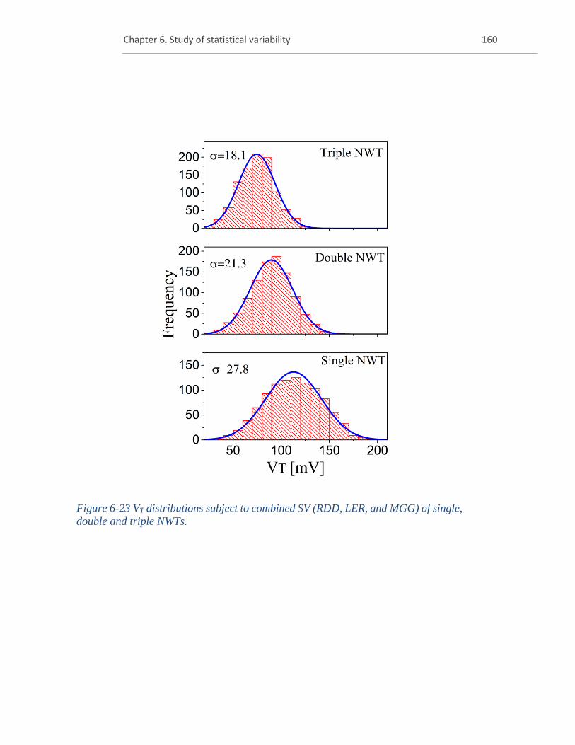
Chapter 6. Study of statistical variability 160
Figure 6-23 VT distributions subject to combined SV (RDD, LER, and MGG) of single,
double and triple NWTs.
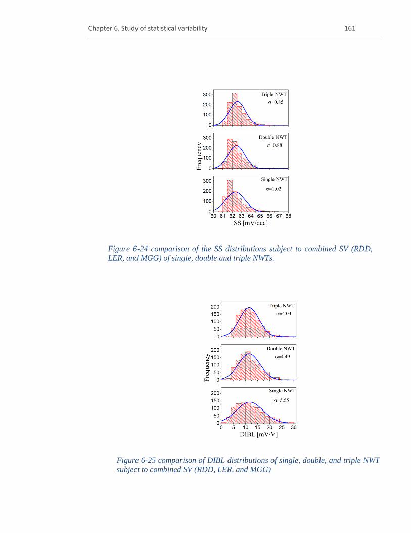
Chapter 6. Study of statistical variability 161
Figure 6-25 comparison of DIBL distributions of single, double, and triple NWT
subject to combined SV (RDD, LER, and MGG)
Figure 6-24 comparison of the SS distributions subject to combined SV (RDD,
LER, and MGG) of single, double and triple NWTs.
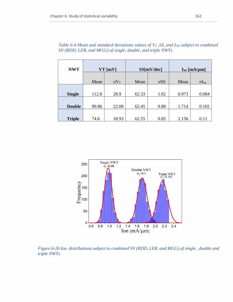
Chapter 6. Study of statistical variability 162
Figure 6-26 Ion distributions subject to combined SV (RDD, LER, and MGG) of single , double and
triple NWTs
Table 6-4 Mean and standard deviations values of VT ,SS, and ION subject to combined
SV (RDD, LER, and MGG) of single, double, and triple NWTs
NWT VT [mV] SS[mV/dec] Ion [mA/µm]
Mean ơVT Mean ơSS Mean σIon
Single 112.8 28.9 62.33 1.02 0.973 0.084
Double 89.86 22.08 62.45 0.88 1.714 0.102
Triple 74.6 18.93 62.55 0.85 2.156 0.11
Chapter 6. Study of statistical variability 163
Additional variability sources
Process variability may be increased due to variation in the cross-sectional shape of the
NWT, based on the fact that electrostatic driven performance and NWT geometry are
corelated. Additionally, VSL NWT performance is determined by the position of lateral
NWTs within the vertical stack. This is due to greater process variability as a result of series
resistance between the S/D contacts and lateral channels.
Summary
The statistical variability of scaled NWT devices with characteristic cross section of 5 nm
and with 12 nm gate length has been explored through extensive simulation and the
corresponding results presented and analysed this chapter. The individual and combined
effects of RDD, LER and MGG on VT, SS, Ion and DIBL have been simulated and
discussed, with the findings suggesting that the key source of variability for all main
electrical parameters considered in this research is MGG. For instance, VT standard
deviation was 1.9 mV under RDD, 5.8 mV under LER, and 27.8 mV under MGG; with Ion
standard deviation being 0.0316 mA/um under RDD, 0.0312 mA/um under LER, and 0.0733
mA/um under MGG.
The results also indicate that NWT variability is impacted by cross-section shape and
dimensions, with a significant reduction in SV found in NWTs with optimal aspect ratios.
Furthermore, a reduction in the variability of threshold voltage drive current are observed in
vertically-stacked NWTs. As noted, the reduction in ơVT found in vertically-stacked NWTs
is due to the cancelling-out of variability in double lateral and triple-channel NWTs.
Chapter 7. Conclusions and Future work 164
7 Chapter 7. Conclusions and Future work
Conclusions
This PhD study was carried out with the primary objective of simulating and optimising a
realistically-scaled Si NWTs suitable for and beyond the 5nm CMOS technology generation.
We have adopted a simulation approach that could effectively reflect quantum confinement
effects with non-equilibrium transport. The aim of this thesis is to carry out comprehensive
TCAD simulation research in order to study the physics of silicon nanowire transistor
devices at the ultimate scaling limits. With the advanced modelling tools employed in this
study, the performance limits of Si NWTs near the end of the CMOS technology scaling
have been evaluated and important challenges in NWT device design have been addressed.
Chapter two describes the challenges that need to be addressed in scaling of conventional
MOSFETs and presents the technology innovations that have been implemented and
proposed for the future. The theory of the MOSFET scaling is also outlined.
The relentless requirement for high-performance and low power devices with ever
increasing density of integration drives the CMOS technology to the ultimate nanoscale
dimensions. Nanowire MOSFETs transistors (NWTs) are among the candidates to extend
CMOS downscaling to ultimate limits, eventually replacing the triple gate FinFET
architectures after the 7nm CMOS technology generation. The nanowire gate-all-around
configuration has the best immunity against short channel effects (SCE) allowing ultimate
transistor scaling. Since statistical variability is becoming a serious scaling limitation factor,
the sources of statistical variability have been discussed in detail.
Semiconductor device design and optimisation depend highly on the accurate simulation of
the device’s physical behaviour and electrical characteristics. By modelling semiconductor
device behaviour as part of the CMOS Technology Computer Aided Design (TCAD)
Chapter 7. Conclusions and Future work 165
process, we can assess its key parameters and operation and understand how to improve its
functionality and performance.
Chapter three has outlined the basis of the 3D drift/diffusion simulation, presenting both the
drift/diffusion (DD) system of semiconductor equations and the density gradient approach
to introduce quantum corrections in the DD system as well as the algorithms employed solve
them self consistently.
In this study we also use the 3D ensemble MC simulation approach with accurate quantum
corrections for the predictive simulation of nanowire transistor (NWT) charge transport and
performance. For the simulation of large multichannel NWTs and for the simulation of
statistical variability we use drift diffusion simulations thoroughly calibrated to the results
of the Monte Carlo simulations. It was clarified that non-equilibrium transport effects in
nano-scale devices cannot be represented by the DD model. Furthermore, transport
variability due to ionised impurity scattering is also difficult to capture using DD-
simulation. Monte Carlo simulation are used to calibrate the drift-diffusion simulations of
large multichannel NWTs and to perform statistical variability simulations. Self-consistent
Poisson- Schrödinger solver is adopted for studying the impact of the quantum confinement
on the mobile chare and capacitance of NWTs with different cross section.
Chapter four examines the ultimate scaling limits of NWTs with different cross-sectional
shapes, using simulations employing Poisson Schrodinger (PS) quantum corrections
implemented in the ‘atomistic’ drift-diffusion (DD) simulator GARAND [GSS]. Realistic
design parameters of the source-drain extensions and their impact on SS and DIBL are
considered. In addition, the effect of the nanowire cross-sectional shape on the gate
capacitance, the charge available for transport and the speed are investigated and discussed.
Signatures of isotropic charge distributions within Si NWTs were observed exhibiting the
same attributes as the golden ratio (Phi), the significance of which is well known in the fields
of art and architecture. The research demonstrates that the quantity of mobile charge within
the channel, along with the intrinsic speed of the device are determined by device geometry
and may be related to the golden AR (Phi) of the nanowire transistors. This investigation
Chapter 7. Conclusions and Future work 166
has demonstrated that NWT with aspect ratios equal or close to the golden ratio (Phi) can
enhance gate capacitance and mobile charge in the channel and therefore could optimise the
intrinsic speed of the device. This study has also investigated the influences of the gate
length on the time delay and the main FoM, such as VT, IOFF and ION and DIBL.
In chapter five, quantum-corrected Monte Carlo simulations are used when exploring
nonequilibrium transport in NWTs’ suitable for the 5nm CMOS technology generation. The
simulations were performed in order to assess whether the semiconductor industry targets
can be met through the use of a single-channel NWT. It was found that this is not possible
with the saturation current falling short of the target value of 15% increase in the saturation
current. The simulations also reveal that NWT saturation current, still does not meet the
target even if high tensile strain is introduced in the channel of single nanowire NWT. Whilst
the quantum-corrected MC simulations are effective in predicting the transistor performance
in the case of small single channel NWTs, they cannot take into account the S/D contact
resistance. Additionally, the MC simulation approach is highly time- and memory-intensive
when simulating stacked NWTs. Following calibration (based on the gate work function,
density gradient confinement effective mass, and mobility models and their relevant
parameters), the DD simulation approach was adopted for the simulation of vertically-
stacked NWTs.
The calibrated DD simulations have revealed that the industrial target value of the drive
current can be met by NWTs with two vertically-stacked lateral channels and highly-doped
S/D regions. This being said, the current is greater in the top nanowire compared to the
bottom nanowire, since the top nanowire is closer to the S/D contact. The reason for this is
the voltage decrease due to the S/D access resistance, and this can result in faster degradation
of the top nanowire with time. A more uniform current density can be achieved by the side
placement of the S/D contacts. Additionally, NWT performance was found to be optimised
when using NWT shapes with aspect ratios similar to the golden ratio (Phi), based on the
exploration of the impacts of Phi on 5 nm CMOS n-type silicon nanowire transistor
performance and electrostatic integrity.
Chapter 7. Conclusions and Future work 167
The impact of variability sources in the DD-based simulator is then presented in Chapter
six. The individual and combined effects of RDD, LER and MGG on VT, SS, Ion and DIBL
have been simulated and discussed, with the findings suggesting that the key source of
variability for all main electrical parameters considered in this research is MGG. For
instance, the VT standard deviation was 1.9 mV under RDD, 5.8 mV under LER, and 27.8
mV under MGG; with Ion standard deviation being 0.0316 mA/um under RDD, 0.0312
mA/um under LER, and 0.0733 mA/um under MGG.
The results also indicate that NWT variability is impacted by cross-section shape and
dimensions, with a significant reduction in SV found in NWTs with optimal aspect ratios.
Furthermore, a reduction in the variability of threshold voltage and drive current are
observed in vertically-stacked NWTs. As noted, the reduction in ơVT found in vertically-
stacked NWTs is due to the cancelling-out of variability in double lateral and triple-channel
NWTs. Additionally, device performance was also found to be significantly driven by the
vertical position of lateral NWTs in the vertical stack as a result of the heightened process
variability caused by series resistance between the S/D contacts and lateral channels.
Overall, the results of this study indicate that NWTs may be a valuable option as next
generation transistor for industry application.
Contributions
The main contributions of this study is the finding that multichannel NWT are suitable
candidates for the 5nm technology node meeting the performance targets and the pitch
requirements. Some of the other important contributions are summarized as follows:
1- Developed novel methodology for DG calibration against more physical PS solution. The
study has demonstrated that after careful calibration against the PS results the DG approach
can be used for practical 3-D simulations of NWTs [7], [9].
Chapter 7. Conclusions and Future work 168
2- For the first time we have studied in details the impact of the quantum mechanical effect
on the electrostatically driven performance of NWTs suitable for a 5 nm CMOS technology
and beyond. We have demonstrated that the NWT shape has a strong impact on the gate
capacitance and the mobile charge in the NWTs at high gate bias. The quantum mechanical
confinement results in a reduction in the mobile charge, gate capacitance, and intrinsic speed
[9], [162], [185], [240].
3- An interesting observation was made in this research regarding the fact that the signatures
of isotropic charge distributions in silicon nanowire transistors (NWT) displayed identical
characteristics to the golden ratio (Phi). In turn, a simulation was conducted regarding ultra-
scaled n-type Si (NWT) suitable for 5-nmCMOS technology and beyond. The results reveal
that the amount of mobile charge in the channel and the intrinsic speed of the device are
determined by the device geometry and could also be correlated to the golden ratio (Phi)
[185], [186].
4- Ensemble Monte Carlo (MC) simulations with quantum correction are used to predict
accurately the drive current of Si (NWT). The complex the carrier transport in the vertically
stacked lateral NWTs and their performance are evaluated using novel methodology
involving the thorough calibration of the current in a single channel to accurate reference
MC simulations.[162], [164], [188], [189]
5- We have investigated the correlation between channel strain and device performance in
various n-type Si- NWTs suitable for 5-nmCMOS technology and beyond. We have
establish a correlation between strain, gate length and a cross-section dimension of the
transistors [189].
6- Our simulations have shown that a single nanowire transistor even with strained Si
channel will not be able to provide the required drive current in comparison to the industrial
target at 5nm CMOS technology generation [164], [188].
Chapter 7. Conclusions and Future work 169
7- Based on predictive simulations have proposes a “vertically stacked lateral NWTs”
structure for the 5-nm CMOS technology that meets the required industry scaling projection
[164], [185].
8- The current density degrades from the top to the bottom of identically sized lateral NWTs
in the vertical stack. The upper lateral nanowires, closer to the source/drain contacts carry
more current than the ones that are farther away (close to the bottom) due to the series
resistance related voltage drop and may become weak point suffering extensive ageing.
Solutions including the idea of increasing the diameter of lower nanowires concerning the
upper nanowires in the stack. However, although the drain current is increased with the
increase of the NWT cross-sectional area, the voltage drop will increase across the highly
doped S/D regions. Furthermore, the possibility of decreasing the doping concentrations
near the top lateral NWT and increasing it gradually near the middle and the bottom lateral
NWTs would decrease the total drain current (Ion). Therefore, we have developed strategy
to optimise S/D contacting by the deformation of S/D contacts [16] [17].
9- For the first time we have carried a comprehensive computational study of the impact of
the principal sources of statistical variability including RDD, LER, and MGG, on the
threshold voltage, drain-induced barrier lowering, and drive current of vertically stacked
lateral NWTs suitable for the 5-nm CMOS technology [164], [185].
10- We have investigated for the first time the position dependent performance and
geometrical variation of the lateral nanowires in the stack as new sources of process
variability (IWCN17).
11- We have found that VT standard deviation of triple lateral stacked NWTs has a lower
standard deviation (ơ) than the double stacked NWTs while the value of ơVT for a single
NWT shows the highest ơ compared with double and triple NWTs [164].
Chapter 7. Conclusions and Future work 170
Recommendations
It will be useful if future research focuses on the optimisation of power and/or performance
of ultimately scaled NWT beyond the 5nm CMOS technology optimising carrier mobility,
electrostatics and parasitic capacitance in order to determine the value of NWT devices.
Mobility tends to suffer as a result of quantum confinement effects in conventional 5 nm
NWTs, caused by phonon and surface roughness scatting. Alternative materials may need
to be adopted to improve carrier transport as the scaling continues, with SiGe (offering better
hole transport) and Ge (offering better electron and hole mobility) recommended for this
purpose. Furthermore, decreasing the effects of fringing field capacitance could enhance
NWT performance. At high frequencies, NWTs with a diamond-shaped S/D structure might
have good performance.
Greater transistor performance can be achieved through the employment of 3D integration
and vertical channel orientation, resulting in more favourable circuit delay and greater
performance due to better per-footprint effective width. This approach can be applied to
NWTs, with nanosheet structures providing an interesting alternative for optimising the
effective width per layout footprint. This should maintain power density whilst enhancing
drive current. The effective width per layout footprint is smaller in nanosheets than in regular
NWTs. Using a thin and wide nanosheet, the effective width can be increased significantly
in comparison to conventional NWTs. A greater effective width along with improved overall
performance can be achieved through the use of a wider nanosheet due to the larger footprint,
while short channel effects remaining unchanged.
There are still many technological and simulation issues associated with the advancement
of NWTs and nanosheet transistor technologies, including the optimisation of shape with a
decrease in roughness, inner spacer, access optimisation and strain management. However,
recent testing and research have demonstrated the value of this alternative configuration to
the future scaling and development of the industry. Therefore, we recommend further study
of the positive impact of device width on performance, highlighting the potential benefits of
nanosheet transistors in the optimisation of future CMOS applications.
Chapter 7. Conclusions and Future work 171
The scaling NWTs beyond 3nm CMOS technology is high challenge, expecting that in the
end the horizontal configuration (such as lateral nanosheet) will punch physics limits. The
vertical configuration of NWTs transforms the layout configuration from a 2D to a 3D,
where the gate length can be extended without occupation a wide area on the wafer. This
technology requires intensive research of design co-optimization.
References 172
8 References
[1] S. K. Moore, “EUV lithography finally ready for fabs,” IEEE Spectr., vol. 55, no. 1, pp.
46–48, Jan. 2018.
[2] J. Chang et al., “A 7nm 256Mb SRAM in high-k metal-gate FinFET technology with
write-assist circuitry for low-VMIN applications,” in 2017 IEEE International Solid-
State Circuits Conference (ISSCC), 2017, pp. 206–207.
[3] S.-Y. Wu et al., “A 7nm CMOS platform technology featuring 4 th generation FinFET
transistors with a 0.027um 2 high density 6-T SRAM cell for mobile SoC applications,”
in 2016 IEEE International Electron Devices Meeting (IEDM), 2016, p. 2.6.1-2.6.4.
[4] V. Moroz, J. Huang, and M. Choi, “FinFET/nanowire design for 5nm/3nm technology
nodes: Channel cladding and introducing a ‘bottleneck’ shape to remove performance
bottleneck,” in 2017 IEEE Electron Devices Technology and Manufacturing Conference
(EDTM), 2017, vol. 3, pp. 67–69.
[5] J. B. Chang et al., “Scaling of SOI FinFETs down to fin width of 4 nm for the 10nm
technology node,” 2011 Symp. VLSI Technol. - Dig. Tech. Pap., pp. 12–13, 2011.
[6] V. Moroz, J. Huang, and R. Arghavani, “Transistor design for 5nm and beyond: Slowing
down electrons to speed up transistors,” in 2016 17th International Symposium on Quality
Electronic Design (ISQED), 2016, vol. 2016–May, pp. 278–283.
[7] Y. Wang et al., “Simulation Study of the Impact of Quantum Confinement on the
Electrostatically Driven Performance of n-type Nanowire Transistors,” IEEE Trans.
Electron Devices, vol. 62, no. 10, pp. 3229–3236, Oct. 2015.
[8] T. Al-Ameri, Y. Wang, V. P. Georgiev, F. Adamu-Lema, X. Wang, and A. Asenov,
“Correlation between gate length, geometry and electrostatic driven performance in ultra-
scaled silicon nanowire transistors,” in 2015 IEEE Nanotechnology Materials and
Devices Conference (NMDC), 2015, pp. 1–5.
References 173
[9] T. Al-Ameri et al., “Impact of quantum confinement on transport and the electrostatic
driven performance of silicon nanowire transistors at the scaling limit,” Solid. State.
Electron., vol. 129, pp. 73–80, Mar. 2017.
[10] H. Mertens et al., “Vertically stacked gate-all-around Si nanowire CMOS transistors with
dual work function metal gates,” in 2016 IEEE International Electron Devices Meeting
(IEDM), 2016, p. 19.7.1-19.7.4.
[11] H. Mertens et al., “Gate-all-around MOSFETs based on vertically stacked horizontal Si
nanowires in a replacement metal gate process on bulk Si substrates,” in 2016 IEEE
Symposium on VLSI Technology, 2016, no. 1, pp. 1–2.
[12] N. Loubet et al., “Stacked nanosheet gate-all-around transistor to enable scaling beyond
FinFET,” in 2017 Symposium on VLSI Technology, 2017, vol. 5, no. 1, pp. T230–T231.
[13] M. H. Na, E. J. Nowak, W. Haensch, and J. Cai, “The effective drive current in CMOS
inverters,” in Digest. International Electron Devices Meeting, 2002, pp. 121–124.
[14] D. Kahng, “A historical perspective on the development of MOS transistors and related
devices,” IEEE Trans. Electron Devices, vol. 23, no. 7, pp. 655–657, Jul. 1976.
[15] Sah Chih-Tang, “Evolution of the MOS transistor-from conception to VLSI,” Proc.
IEEE, vol. 76, no. 10, pp. 1280–1326, 1988.
[16] J. E. Lilienfeld, “Method and apparatus for controlling electric currents,” US Patent
1,745,175. pp. 1–4, 1930.
[17] N. Arora, MOSFET Models for VLSI Circuit Simulation. Vienna: Springer Vienna, 1993.
[18] G. E. Moore, “Cramming More Components Onto Integrated Circuits,” Proc. IEEE, vol.
86, no. 1, pp. 82–85, Jan. 1998.
[19] M. Guarnieri, “The Unreasonable Accuracy of Moore’s Law [Historical],” IEEE Ind.
Electron. Mag., vol. 10, no. 1, pp. 40–43, Mar. 2016.
[20] K. Ahmed and K. Schuegraf, “Transistor wars,” IEEE Spectr., vol. 48, no. 11, pp. 50–66,
2011.
References 174
[21] W. M. Holt, “1.1 Moore’s law: A path going forward,” Dig. Tech. Pap. - IEEE Int. Solid-
State Circuits Conf., vol. 59, pp. 8–13, 2016.
[22] E. P. DeBenedictis, “It’s Time to Redefine Moore’s Law Again,” Computer (Long.
Beach. Calif)., vol. 50, no. 2, pp. 72–75, Feb. 2017.
[23] R. K. Cavin, P. Lugli, and V. V Zhirnov, “Science and Engineering Beyond Moore’s
Law,” Proc. IEEE, vol. 100, no. Special Centennial Issue, pp. 1720–1749, May 2012.
[24] R. Guldi et al., “Systematic and random defect reduction during the evolution of
integrated circuit technology,” in 10th Annual IEEE/SEMI. Advanced Semiconductor
Manufacturing Conference and Workshop. ASMC 99 Proceedings (Cat.
No.99CH36295), 1999, pp. 2–7.
[25] K. J. Kuhn, “CMOS scaling beyond 32nm,” in Proceedings of the 46th Annual Design
Automation Conference on ZZZ - DAC ’09, 2009, p. 310.
[26] ITRS, “International Technology Roadmap for Semiconductors 2.0: Executive Report,”
Int. Technol. roadmap Semicond., p. 79, 2015.
[27] M. Bhushan and M. B. Ketchen, CMOS Test and Evaluation. New York, NY: Springer
New York, 2015.
[28] K. C. Saraswat, D. Kim, T. Krishnamohan, and A. Pethe, “Performance Limitations of
Si Bulk CMOS and Alternatives for future ULSI,” in ECS Transactions, 2007, vol. 8, no.
3, pp. 9–14.
[29] J. Robertson, “High dielectric constant oxides,” Eur. Phys. J. Appl. Phys., vol. 28, no. 3,
pp. 265–291, Dec. 2004.
[30] J. D. Plummer and P. B. Griffin, “Material and process limits in silicon VLSI
technology,” Proc. IEEE, vol. 89, no. 3, pp. 240–258, Mar. 2001.
[31] A. S. M. Zain, “Scaling and Variability in Ultra Thin Body Silicon on Insulator ( UTB
SOI ) MOSFETs Anis Suhaila Mohd Zain,” University of Glasgow, 2013.
[32] F. Adamu-Lema, “Scaling and Intrinsic Parameter Fluctuations in Nano-CMOS
References 175
Devices,” University of Glasgow, 2005.
[33] J. Sivagnaname and R. B. Brown, “Effect of scaling on stand-by current in PD-SOI
pseudo-nMOS circuits,” in 2003 46th Midwest Symposium on Circuits and Systems,
2004, vol. 3, pp. 1560–1562.
[34] T. Numata et al., “Performance enhancement of partially and fully depleted strained-SOI
MOSFETs,” IEEE Trans. Electron Devices, vol. 53, no. 5, pp. 1030–1038, May 2006.
[35] D. Munteanu, S. Cristoloveanu, and O. Faynot, “Transition from generation- to
recombination-based transients in partially depleted SOI MOSFETs,” in 1998 IEEE
International SOI Conference Proceedings (Cat No.98CH36199), 1998, pp. 71–72.
[36] S. Okhonin, M. Nagoga, and P. Fazan, “Principles of transient charge pumping on
partially depleted SOI MOSFETs,” IEEE Electron Device Lett., vol. 23, no. 5, pp. 279–
281, May 2002.
[37] W. Zhao, J. He, R. E. Belford, L.-E. Wernersson, and A. Seabaugh, “Partially Depleted
SOI MOSFETs Under Uniaxial Tensile Strain,” IEEE Trans. Electron Devices, vol. 51,
no. 3, pp. 317–323, Mar. 2004.
[38] F. Dieudonne, J. Jomaah, and F. Balestra, “Gate-induced floating body effect excess
noise in partially depleted SOI MOSFETs,” IEEE Electron Device Lett., vol. 23, no. 12,
pp. 737–739, Dec. 2002.
[39] Okhonin, Nagoga, and Fazan, “Charge pumping effects in partially depleted SOI
MOSFETs,” in 2003 IEEE International Conference on Robotics and Automation (Cat
No 03CH37422) SOI-03), 2003, pp. 74–75.
[40] Casu and Flatresse, “History effect characterization in PD-SOI CMOS gates,” in IEEE
International SOI Conference SOI-02, 2002, pp. 62–63.
[41] S. Kawanaka et al., “Body voltage and history effect sensitivity to key device parameters
in 90 nm PD-SOI,” in 2004 IEEE International SOI Conference (IEEE Cat.
No.04CH37573), 2004, pp. 19–20.
[42] Q. Liang et al., “Optimizing History Effects in 65nm PD-SOI CMOS,” in 2006 IEEE
References 176
international SOI Conferencee Proceedings, 2006, vol. 75, no. 3, pp. 95–96.
[43] A. Marshall and S. Natarajan, “PD-SOI and FD-SOI: a comparison of circuit
performance,” in 9th International Conference on Electronics, Circuits and Systems,
2002, vol. 1, pp. 25–28.
[44] S. K. Pandey and G. Saini, “Study of self-heating effects on fully depleted SOI MOSFETs
with BOX layer engineering,” in 2017 International Conference on Trends in Electronics
and Informatics (ICEI), 2017, pp. 962–965.
[45] C. Baltaci and Y. Leblebici, “Self-heating effects on the thermal noise of deep sub-micron
FD-SOI MOSFETs,” in 2017 13th Conference on Ph.D. Research in Microelectronics
and Electronics (PRIME), 2017, pp. 229–232.
[46] R. K. Lawrence, G. J. Campisi, G. J. Shontz, G. Pollack, and R. Sundaresan, “Limitations
to fully-depleted SOI structures,” in 1990 IEEE SOS/SOI Technology Conference.
Proceedings, 1990, pp. 101–102.
[47] J. G. Fossum, P.-C. Yeh, and J. Y. Choi, “Floating-body problems and benefits in fully
depleted SOI CMOS VLSI circuits,” in International Electron Devices Meeting 1991
[Technical Digest], 1991, no. 1, pp. 325–328.
[48] J.-S. Lyu and C. Lee, “Allowable surface silicon thickness for fully-depleted SOI
MOSFET’s,” in 1991 IEEE International SOI Conference Proceedings, 1991, pp. 56–57.
[49] R. Gallegos and M. Sullivan, “Salicide technology for fully-depleted SOI CMOS
devices,” in 1990 IEEE SOS/SOI Technology Conference. Proceedings, 1990, pp. 79–80.
[50] J.-P. Colinge, “Some properties of thin-film SOI MOSFETs,” IEEE Circuits Devices
Mag., vol. 3, no. 6, pp. 16–20, Nov. 1987.
[51] K. Suzuki, T. Tanaka, Y. Tosaka, H. Horie, and Y. Arimoto, “Scaling theory for double-
gate SOI MOSFET’s,” IEEE Trans. Electron Devices, vol. 40, no. 12, pp. 2326–2329,
1993.
[52] M. Vinet et al., “Bonded planar double-metal-gate NMOS transistors down to 10 nm,”
IEEE Electron Device Lett., vol. 26, no. 5, pp. 317–319, May 2005.
References 177
[53] D. Hisamoto, T. Kaga, and E. Takeda, “Impact of the vertical SOI ‘DELTA’ structure on
planar device technology,” IEEE Trans. Electron Devices, vol. 38, no. 6, pp. 1419–1424,
Jun. 1991.
[54] G. Vellianitis et al., “Gatestacks for scalable high-performance FinFETs,” in 2007 IEEE
International Electron Devices Meeting, 2007, pp. 681–684.
[55] C. Auth et al., “A 10nm high performance and low-power CMOS technology featuring
3 rd generation FinFET transistors, Self-Aligned Quad Patterning, contact over active
gate and cobalt local interconnects,” in 2017 IEEE International Electron Devices
Meeting (IEDM), 2017, p. 29.1.1-29.1.4.
[56] Xuejue Huang et al., “Sub 50-nm FinFET: PMOS,” in International Electron Devices
Meeting 1999. Technical Digest (Cat. No.99CH36318), 1999, pp. 67–70.
[57] S. Barraud et al., “Performance of Omega-Shaped-Gate Silicon Nanowire MOSFET
With Diameter Down to 8 nm,” IEEE Electron Device Lett., vol. 33, no. 11, pp. 1526–
1528, Nov. 2012.
[58] T.-K. Chiang, “A Novel Scaling Theory for Fully Depleted Omega-Gate MOSFETs
Included With Equivalent Number of Gates,” IEEE Trans. Electron Devices, vol. 61, no.
3, pp. 926–929, Mar. 2014.
[59] C. Dupre et al., “15nm-diameter 3D stacked nanowires with independent gates operation:
ΦFET,” in 2008 IEEE International Electron Devices Meeting, 2008, no. c, pp.
1–4.
[60] L. Wang, A. Shafaei, and M. Pedram, “Gate-all-around FET based 6T SRAM design
using a device-circuit co-optimization framework,” in 2017 IEEE 60th International
Midwest Symposium on Circuits and Systems (MWSCAS), 2017, vol. 2017–Augus, pp.
1113–1116.
[61] A. Veloso et al., “Junctionless gate-all-around lateral and vertical nanowire FETs with
simplified processing for advanced logic and analog/RF applications and scaled SRAM
cells,” in 2016 IEEE Symposium on VLSI Technology, 2016, vol. 2016–Septe, pp. 1–2.
References 178
[62] A. Chasin et al., “Complete degradation mapping of stacked gate-all-around Si nanowire
transistors considering both intrinsic and extrinsic effects,” in 2017 IEEE International
Electron Devices Meeting (IEDM), 2017, p. 7.1.1-7.1.4.
[63] D. Yakimets et al., “Vertical GAAFETs for the Ultimate CMOS Scaling,” IEEE Trans.
Electron Devices, vol. 62, no. 5, pp. 1433–1439, May 2015.
[64] L. Geppert, “The amazing vanishing transistor act,” IEEE Spectr., vol. 39, no. 10, pp. 28–
33, Oct. 2002.
[65] A. . Fallis, Nanoscale Transistors, vol. 53, no. 9. Boston: Kluwer Academic Publishers,
2006.
[66] J.-P. Colinge, FinFETs and Other Multi-Gate Transistors. Boston, MA: Springer US,
2008.
[67] K. K. Young, “Short-channel effect in fully depleted SOI MOSFETs,” IEEE Trans.
Electron Devices, vol. 36, no. 2, pp. 399–402, 1989.
[68] R.-H. Yan, A. Ourmazd, and K. F. Lee, “Scaling the Si MOSFET: from bulk to SOI to
bulk,” IEEE Trans. Electron Devices, vol. 39, no. 7, pp. 1704–1710, Jul. 1992.
[69] D. Hisamoto, T. Kaga, Y. Kawamoto, and E. Takeda, “A fully depleted lean-channel
transistor (DELTA)-a novel vertical ultra thin SOI MOSFET,” in International Technical
Digest on Electron Devices Meeting, 1989, pp. 833–836.
[70] S. Kong, “Finfet transistor structures having a double gate channel extending vertically
from a substrate and methods of manufacture,” US 6413 802 B1, 2002.
[71] C. Auth et al., “A 22nm high performance and low-power CMOS technology featuring
fully-depleted tri-gate transistors, self-aligned contacts and high density MIM
capacitors,” in 2012 Symposium on VLSI Technology (VLSIT), 2012, vol. m, no. 2003,
pp. 131–132.
[72] C.-H. Jan et al., “A 22nm SoC platform technology featuring 3-D tri-gate and high-
k/metal gate, optimized for ultra low power, high performance and high density SoC
applications,” in 2012 International Electron Devices Meeting, 2012, p. 3.1.1-3.1.4.
References 179
[73] Y. Li and C. H. Hwang, “Effect of fin angle on electrical characteristics of nanoscale
round-top-gate bulk FinFETs,” IEEE Trans. Electron Devices, vol. 54, no. 12, pp. 3426–
3429, 2007.
[74] S. Natarajan et al., “A 14nm logic technology featuring 2nd-generation FinFET, air-
gapped interconnects, self-aligned double patterning and a 0.0588 um2 SRAM cell size,”
in 2014 IEEE International Electron Devices Meeting, 2014, p. 3.7.1-3.7.3.
[75] J. Mitard et al., “A 2nd Generation of 14/16nm-node compatible strained-Ge pFINFET
with improved performance with respect to advanced Si-channel FinFETs,” in 2016 IEEE
Symposium on VLSI Technology, 2016, pp. 1–2.
[76] N. Collaert et al., “Beyond-Si materials and devices for more Moore and more than
Moore applications,” 2016 Int. Conf. IC Des. Technol., pp. 1–5, 2016.
[77] N. Collaert, “Mastering the Art of High Mobility Material Integration on Si: A Path
towards Power-Efficient CMOS and Functional Scaling,” J. Low Power Electron. Appl.,
vol. 6, no. 2, p. 9, 2016.
[78] P. Zheng, D. Connelly, F. Ding, and T.-J. K. Liu, “Inserted-oxide FinFET (iFinFET)
design to extend CMOS scaling,” in 2015 International Symposium on VLSI Technology,
Systems and Applications, 2015, vol. 2015–June, pp. 1–2.
[79] W. Xu, H. Yin, X. Ma, P. Hong, M. Xu, and L. Meng, “Novel 14-nm Scallop-Shaped
FinFETs (S-FinFETs) on Bulk-Si Substrate,” Nanoscale Res. Lett., vol. 10, no. 1, p. 249,
Dec. 2015.
[80] C. Chou, C. Hsu, W.-K. Yeh, S. S. Chung, and C. Chien, “3D-TCAD simulation study
of the contact all around T-FinFET structure for 10nm metal-oxide-semiconductor field-
effect transistor,” in 2016 IEEE Silicon Nanoelectronics Workshop (SNW), 2016, pp.
190–191.
[81] X. He et al., “Impact of aggressive fin width scaling on FinFET device characteristics,”
in 2017 IEEE International Electron Devices Meeting (IEDM), 2017, p. 20.2.1-20.2.4.
[82] S. Bangsaruntip et al., “High performance and highly uniform gate-all-around silicon
References 180
nanowire MOSFETs with wire size dependent scaling,” in 2009 IEEE International
Electron Devices Meeting (IEDM), 2009, pp. 1–4.
[83] R. Kim, U. E. Avci, and I. A. Young, “CMOS performance benchmarking of Si, InAs,
GaAs, and Ge nanowire n- and pMOSFETs with Lg=13 nm based on atomistic quantum
transport simulation including strain effects,” in 2015 IEEE International Electron
Devices Meeting (IEDM), 2015, vol. 2016–Febru, no. 503, p. 34.1.1-34.1.4.
[84] Y. Lee et al., “Diamond-shaped Ge and Ge0.9Si0.1 gate-all-around nanowire FETs with
four 111 facets by dry etch technology,” in 2015 IEEE International Electron Devices
Meeting (IEDM), 2015, p. 15.1.1-15.1.4.
[85] E. Bury et al., “Self-heating in FinFET and GAA-NW using Si, Ge and III/V channels,”
in 2016 IEEE International Electron Devices Meeting (IEDM), 2016, p. 15.6.1-15.6.4.
[86] M. Karner et al., “Vertically stacked nanowire MOSFETs for sub-10nm nodes: Advanced
topography, device, variability, and reliability simulations,” in 2016 IEEE International
Electron Devices Meeting (IEDM), 2016, p. 30.7.1-30.7.4.
[87] S. Bangsaruntip et al., “Density scaling with gate-all-around silicon nanowire MOSFETs
for the 10 nm node and beyond,” in 2013 IEEE International Electron Devices Meeting,
2013, p. 20.2.1-20.2.4.
[88] S. Barraud et al., “Vertically stacked-NanoWires MOSFETs in a replacement metal gate
process with inner spacer and SiGe source/drain,” in 2016 IEEE International Electron
Devices Meeting (IEDM), 2016, p. 17.6.1-17.6.4.
[89] H. Mertens et al., “Vertically stacked gate-all-around Si nanowire transistors: Key
Process Optimizations and Ring Oscillator Demonstration,” in 2017 IEEE International
Electron Devices Meeting (IEDM), 2017, p. 37.4.1-37.4.4.
[90] S. Y. Chou, D. A. Antoniadis, and H. I. Smith, “Observation of electron velocity
overshoot in sub-100-nm-channel MOSFET’s in Silicon,” IEEE Electron Device Lett.,
vol. 6, no. 12, pp. 665–667, Dec. 1985.
[91] J. Wang, “Device Physics and Simulation of Silicon Nanowire Transistor,” Purdue
References 181
University, 2005.
[92] M. V. Dunga, “Nanoscale CMOS Modeling,” University of California at Berkeley, 2008.
[93] M. Lundstrom, “Fundamentals of Carrier Transport, 2nd edn,” Meas. Sci. Technol., vol.
13, no. 2, pp. 230–230, Feb. 2002.
[94] S. Dhar, “Analytical Mobility Modeling for Strained Silicon-Based Devices,” TU Wien,
2007.
[95] C. de Falco, E. Gatti, A. L. Lacaita, and R. Sacco, “Quantum-corrected drift-diffusion
models for transport in semiconductor devices,” J. Comput. Phys., vol. 204, no. 2, pp.
533–561, Apr. 2005.
[96] T. Zibold, “Semiconductor based quantum information devices : Theory and
simulations,” Technical University of Munich, 2007.
[97] A. Asenov, S. Kaya, and J. H. Davies, “Intrinsic threshold voltage fluctuations in
decanano MOSFETs due to local oxide thickness variations,” IEEE Trans. Electron
Devices, vol. 49, no. 1, pp. 112–119, 2002.
[98] A. Asenov, A. R. Brown, J. H. Davies, and S. Saini, “Hierarchical approach to ‘atomistic’
3-D MOSFET simulation,” IEEE Trans. Comput. Des. Integr. Circuits Syst., vol. 18, no.
11, pp. 1558–1565, 1999.
[99] A. Asenov, “Random dopant induced threshold voltage lowering and fluctuations in sub-
0.1 fjim MOSFET’s: A 3-D ‘atomistic’ simulation study,” IEEE Trans. Electron Devices,
vol. 45, no. 12, pp. 2505–2513, 1998.
[100] R. Granzner, V. . Polyakov, F. Schwierz, M. Kittler, and T. Doll, “On the suitability of
DD and HD models for the simulation of nanometer double-gate MOSFETs,” Phys. E
Low-dimensional Syst. Nanostructures, vol. 19, no. 1–2, pp. 33–38, Jul. 2003.
[101] C. Riddet, “Monte Carlo study of current variability in UTB SOI DG MOSFETs,”
University of Glasgow, 2010.
[102] M. Lundstrom and S. Datta, “Physical device simulation in a shrinking world,” IEEE
References 182
Circuits Devices Mag., vol. 6, no. 4, pp. 32–37, Jul. 1990.
[103] G. A. Sai-Halasz, M. R. Wordeman, D. P. Kern, S. Rishton, and E. Ganin, “High
transconductance and velocity overshoot in NMOS devices at the 0.1- mu m gate-length
level,” IEEE Electron Device Lett., vol. 9, no. 9, pp. 464–466, Sep. 1988.
[104] F. M. Bufler, A. Schenk, and W. Fichtner, “Monte Carlo, Hydrodynamic and Drift-
Diffusion Simulation of Scaled Double-Gate MOSFETs,” J. Comput. Electron., vol. 2,
no. 2–4, pp. 81–84, Dec. 2003.
[105] A. Afzalian, C.-W. Lee, N. Dehdashti Akhavan, R. Yan, I. Ferain, and J.-P. Colinge,
“Quantum Confinement Effects in Capacitance Behavior of Multigate Silicon Nanowire
MOSFETs,” IEEE Trans. Nanotechnol., vol. 10, no. 2, pp. 300–309, 2011.
[106] Y. Yamada, H. Tsuchiya, and M. Ogawa, “Quantum transport simulation of silicon-
nanowire transistors based on direct solution approach of the Wigner transport equation,”
Electron Devices, IEEE …, vol. 56, no. 7, pp. 1396–1401, 2009.
[107] M. H.-S. Jin Seong-Hoon, Park Young-June, “Simulation of Quantum Effects in the
Nano-scale Semiconductor Device.pdf.” Journal of Semiconductor Technology and
Science, pp. 32–40, 2004.
[108] J. A. Greenfield and R. W. Dutton, “Nonplanar VLSI Device Analysis Using the Solution
of Poisson’s Equation,” IEEE J. Solid-State Circuits, vol. 15, no. 4, pp. 585–597, Aug.
1980.
[109] J. A. Greenfield and R. W. Dutton, “Nonplanar VLSI device analysis using the solution
of Poisson’s equation,” IEEE Trans. Electron Devices, vol. 27, no. 8, pp. 1520–1532,
Aug. 1980.
[110] H. A. van der Vorst, “Bi-CGSTAB: A Fast and Smoothly Converging Variant of Bi-CG
for the Solution of Nonsymmetric Linear Systems,” SIAM J. Sci. Stat. Comput., vol. 13,
no. 2, pp. 631–644, Mar. 1992.
[111] C. Millar, A. Asenov, and J. R. Watling, “Excessive Over-Relaxation Method for
Multigrid Poisson Solvers,” J. Comput. Electron., vol. 1, no. 3, pp. 341–345, 2002.
References 183
[112] C. Jacoboni and L. Reggiani, “The Monte Carlo method for the solution of charge
transport in semiconductors with applications to covalent materials[J],” Rev. Mod. Phys.,
vol. 55, no. 3, pp. 645–705, 1983.
[113] C. C. Moglestue, “A Self-Consistent Monte Carlo Particle Model to Analyze
Semiconductor Microcomponents of any Geometry,” IEEE Trans. Comput. Des. Integr.
Circuits Syst., vol. 5, no. 2, pp. 326–345, Apr. 1986.
[114] F. M. Bufler, A. Schenk, and W. Fichtner, “Efficient Monte Carlo device modeling,”
IEEE Trans. Electron Devices, vol. 47, no. 10, pp. 1891–1897, 2000.
[115] S. E. Laux, A. Kumar, and M. V. Fischetti, “Analysis of quantum ballistic electron
transport in ultrasmall silicon devices including space-charge and geometric effects,” J.
Appl. Phys., vol. 95, no. 10, pp. 5545–5582, May 2004.
[116] B. Ghosh, X. Wang, X.-F. Fan, L. F. Register, and S. K. Banerjee, “Monte Carlo Study
of Germanium n- and pMOSFETs,” IEEE Trans. Electron Devices, vol. 52, no. 4, pp.
547–553, Apr. 2005.
[117] M. V Fischetti, S. E. Laux, and E. Crabbé, “Understanding hot‐electron transport in
silicon devices: Is there a shortcut?,” J. Appl. Phys., vol. 78, no. 2, pp. 1058–1087, Jul.
1995.
[118] M. V. Fischetti, S. E. Laux, P. M. Solomon, and A. Kumar, “Thirty Years of Monte Carlo
Simulations of Electronic Transport in Semiconductors: Their Relevance to Science and
Mainstream VLSI Technology,” J. Comput. Electron., vol. 3, no. 3–4, pp. 287–293, Oct.
2004.
[119] C. Riddet, C. Alexander, A. R. Brown, S. Roy, and A. Asenov, “Simulation of ‘Ab Initio’
Quantum Confinement Scattering in UTB MOSFETs Using Three-Dimensional
Ensemble Monte Carlo,” IEEE Trans. Electron Devices, vol. 58, no. 3, pp. 600–608, Mar.
2011.
[120] H. Kosina, M. Nedjalkov, and S. Selberherr, “Theory of the Monte Carlo method for
semiconductor device simulation,” IEEE Trans. Electron Devices, vol. 47, no. 10, pp.
References 184
1898–1908, 2000.
[121] G. F. Formicone, M. Saraniti, D. Z. Vasileska, and D. K. Ferry, “Study of a 50 nm
nMOSFET by ensemble Monte Carlo simulation including a new approach to surface
roughness and impurity scattering in the Si inversion layer,” IEEE Trans. Electron
Devices, vol. 49, no. 1, pp. 125–132, 2002.
[122] J. Koga, S. Takagi, and A. Toriumi, “Influences of buried-oxide interface on inversion-
layer mobility in ultra-thin SOI MOSFETs,” IEEE Trans. Electron Devices, vol. 49, no.
6, pp. 1042–1048, Jun. 2002.
[123] S. C. Williams, K. W. Kim, and W. C. Holton, “Ensemble Monte Carlo study of channel
quantization in a 25-nm n-MOSFET,” IEEE Trans. Electron Devices, vol. 47, no. 10, pp.
1864–1872, 2000.
[124] U. Ravaioli, B. Winstead, C. Wordelman, and A. Kepkep, “Monte Carlo simulation for
ultra-small MOS devices,” Superlattices Microstruct., vol. 27, no. 2–3, pp. 137–145, Feb.
2000.
[125] C. L. Alexander, A. R. Brown, J. R. Watling, and A. Asenov, “Impact of Single Charge
Trapping in Nano-MOSFETs—Electrostatics Versus Transport Effects,” IEEE Trans.
Nanotechnol., vol. 4, no. 3, pp. 339–344, May 2005.
[126] C. Alexander, J. Watling, and A. Asenov, “Numerical carrier heating when implementing
P3M to study small volume variations,” Semicond. Sci. Technol., vol. 19, no. 4 SPEC.
ISS., 2004.
[127] C. J. Wordelman and U. Ravaioli, “Integration of a particle-particle-particle-mesh
algorithm with the ensemble Monte Carlo method for the simulation of ultra-small
semiconductor devices,” IEEE Trans. Electron Devices, vol. 47, no. 2, pp. 410–416,
2000.
[128] W. Lee and U. Ravaioli, “A Simple and Efficient Method for the Calculation of Carrier-
Carrier Scattering in Monte-Carlo Simulations,” vol. 3, no. 2, pp. 1–4, 2010.
[129] D. Nagy et al., “3-D Finite Element Monte Carlo Simulations of Scaled Si SOI FinFET
References 185
With Different Cross Sections,” vol. 14, no. 1, pp. 93–100, 2015.
[130] H. Kubotera et al., “Efficient Monte Carlo simulation of ion implantation into 3D FinFET
structure,” in 2014 20th International Conference on Ion Implantation Technology (IIT),
2014, pp. 1–4.
[131] M. Aldegunde and K. Kalna, “Self-Forces in 3D Finite Element Monte Carlo Simulations
of a 10 . 7 nm Gate Length SOI FinFET,” no. 2, pp. 185–188, 2014.
[132] G. Du, W. Zhang, J. Wang, T. Lu, P. Zhang, and X. Liu, “Study of 20nm bulk FINFET
by using 3D full band Monte Carlo method with Effective Potential Quantum
Correction,” in 2010 10th IEEE International Conference on Solid-State and Integrated
Circuit Technology, 2010, pp. 1952–1954.
[133] F. M. Bufler, L. Sponton, and A. Erlebach, “FinFET stress engineering using 3D
mechanical stress and 2D Monte Carlo device simulation,” in ESSDERC 2008 - 38th
European Solid-State Device Research Conference, 2008, pp. 166–169.
[134] J. Lindberg et al., “Quantum corrections based on the 2-D Schr??dinger equation for 3-
D finite element monte carlo simulations of nanoscaled finfets,” IEEE Trans. Electron
Devices, vol. 61, no. 2, pp. 423–429, 2014.
[135] B. Winstead and U. Ravaioli, “A quantum correction based on schrodinger equation
applied to Monte Carlo device simulation,” IEEE Trans. Electron Devices, vol. 50, no.
2, pp. 440–446, Feb. 2003.
[136] H. Tsuchiya and T. Miyoshi, “Quantum mechanical Monte Carlo approach to electron
transport at heterointerface,” Superlattices Microstruct., vol. 27, no. 5–6, pp. 529–532,
May 2000.
[137] D. K. Ferry, R. Akis, and D. Vasileska, “Quantum effects in MOSFETs: use of an
effective potential in 3D Monte Carlo simulation of ultra-short channel devices,” in
International Electron Devices Meeting 2000. Technical Digest. IEDM (Cat.
No.00CH37138), 2000, pp. 287–290.
[138] S. M. Ramey and D. K. Ferry, “Threshold voltage calculation in ultra-thin film SOI
References 186
MOSFETs using the effective potential,” in Proceedings of the 2nd IEEE Conference on
Nanotechnology, 2002, no. 100, pp. 189–192.
[139] L. Lucci, P. Palestri, D. Esseni, and L. Selmi, “Multi-subband Monte Carlo modeling of
nano-MOSFETs with strong vertical quantization and electron gas degeneration,” vol.
00, no. c, pp. 8–11, 2005.
[140] H. Tsuchiya and U. Ravaioli, “Particle Monte Carlo simulation of quantum phenomena
in semiconductor nanostructures,” vol. 4023, no. 2001, 2010.
[141] P. Palestri, S. Eminente, D. Esseni, C. Fiegna, E. Sangiorgi, and L. Selmi, “An improved
semi-classical Monte-Carlo approach for nano-scale MOSFET simulation,” Solid. State.
Electron., vol. 49, no. 5, pp. 727–732, May 2005.
[142] S. M. Ramey and D. K. Ferry, “3D Monte Carlo Modeling of Thin SOI MOSFETs
Including the Effective Potential and Random Dopant Distribution ∗,” pp. 267–271,
2002.
[143] X. Liu, K. Wei, G. Du, W. Zhang, and P. Zhang, “3D parallel full band ensemble Monte
Carlo devices simulation for nano scale devices application,” in 2012 IEEE 11th
International Conference on Solid-State and Integrated Circuit Technology, 2012, pp. 1–
4.
[144] X.-F. Fan, X. Wang, B. Winstead, L. F. Register, U. Ravaioli, and S. K. Banerjee, “MC
Simulation of Strained-Si MOSFET With Full-Band Structure and Quantum Correction,”
IEEE Trans. Electron Devices, vol. 51, no. 6, pp. 962–970, Jun. 2004.
[145] G. A. Kathawala and U. Ravaioli, “3-D Monte Carlo simulations of FinFETs,” in IEEE
International Electron Devices Meeting 2003, p. 29.2.1-29.2.4.
[146] A. T. Elthakeb, H. Abd Elhamid, and Y. Ismail, “Scaling of TG-FinFETs: 3-D Monte
Carlo Simulations in the Ballistic and Quasi-Ballistic Regimes,” IEEE Trans. Electron
Devices, vol. 62, no. 6, pp. 1796–1802, Jun. 2015.
[147] B. Winstead and H. Tsuchiya, “Comparison of Quantum Corrections for Monte Carlo
Simulation,” J. Comput. Electron., pp. 201–207, 2002.
References 187
[148] G. Masetti, M. Severi, and S. Solmi, “Modeling of carrier mobility against carrier
concentration in arsenic-, phosphorus-, and boron-doped silicon,” IEEE Trans. Electron
Devices, vol. 30, no. 7, pp. 764–769, Jul. 1983.
[149] N. D. Arora, J. R. Hauser, and D. J. Roulston, “Electron and hole mobilities in silicon as
a function of concentration and temperature,” IEEE Trans. Electron Devices, vol. 29, no.
2, pp. 292–295, Feb. 1982.
[150] D. B. M. Klaassen, “A unified mobility model for device simulation—I. Model equations
and concentration dependence,” Solid. State. Electron., vol. 35, no. 7, pp. 953–959, Jul.
1992.
[151] K. Yamaguchi, “Field-dependent mobility model for two-dimensional numerical analysis
of MOSFET’s,” IEEE Trans. Electron Devices, vol. 26, no. 7, pp. 1068–1074, Jul. 1979.
[152] M. N. Darwish, J. L. Lentz, M. R. Pinto, P. M. Zeitzoff, T. J. Krutsick, and Hong Ha
Vuong, “An improved electron and hole mobility model for general purpose device
simulation,” IEEE Trans. Electron Devices, vol. 44, no. 9, pp. 1529–1538, 1997.
[153] S. Reggiani, E. Gnani, A. Gnudi, M. Rudan, and G. Baccarani, “Low-Field Electron
Mobility Model for Ultrathin-Body SOI and Double-Gate MOSFETs With Extremely
Small Silicon Thicknesses,” IEEE Trans. Electron Devices, vol. 54, no. 9, pp. 2204–
2212, Sep. 2007.
[154] D. M. Caughey and R. E. Thomas, “Carrier mobilities in silicon empirically related to
doping and field,” Proc. IEEE, vol. 55, no. 12, pp. 2192–2193, 1967.
[155] C. Canali, G. Majni, R. Minder, and G. Ottaviani, “Electron and hole drift velocity
measurements in silicon and their empirical relation to electric field and temperature,”
IEEE Trans. Electron Devices, vol. 22, no. 11, pp. 1045–1047, Nov. 1975.
[156] M. Mohamed, “3D Electro-Thermal Monte Carlo Study of Transport in Confined Silicon
Devices,” University of Illinois at Urbana-Champaign, 2012.
[157] S. Habicht, “Strained and Unstrained Silicon Nanowire-Array MOSFETs: Fabrication
and Physical Analysis,” 2011.
References 188
[158] L. Donetti et al., “Multi-Subband Ensemble Monte Carlo simulation of Si nanowire
MOSFETs,” in 2015 International Conference on Simulation of Semiconductor
Processes and Devices (SISPAD), 2015, pp. 353–356.
[159] B. Hoefflinger, “ITRS: The International Technology Roadmap for Semiconductors,”
2011, pp. 161–174.
[160] A. C. Elitzur et al., CHIPS 2020 VOL. 2, vol. 2. Cham: Springer International Publishing,
2016.
[161] H. J.M. Veendrick, Nanometer CMOS ICs. Cham: Springer International Publishing,
2017.
[162] A. Asenov et al., “Nanowire transistor solutions for 5nm and beyond,” in 2016 17th
International Symposium on Quality Electronic Design (ISQED), 2016, no. 001, pp. 269–
274.
[163] F. Adamu-Lema et al., “(Invited) Modelling and Simulation of Advanced Semiconductor
Devices,” ECS Trans., vol. 80, no. 4, pp. 33–42, Aug. 2017.
[164] T. Al-Ameri, V. P. Georgiev, F. Adamu-Lema, and A. Asenov, “Simulation Study of
Vertically Stacked Lateral Si Nanowires Transistors for 5-nm CMOS Applications,”
IEEE J. Electron Devices Soc., vol. 5, no. 6, pp. 466–472, Nov. 2017.
[165] C. Dupas, P. Houdy, and M. Lahmani, Nanoscience. Berlin, Heidelberg: Springer Berlin
Heidelberg, 2007.
[166] H. R. Huff and D. C. Gilmer, High Dielectric Constant Materials, vol. 16.
Berlin/Heidelberg: Springer-Verlag, 2005.
[167] R. M. Wallace, “Challenges for the characterization and integration of high-κ dielectrics,”
Appl. Surf. Sci., vol. 231–232, pp. 543–551, Jun. 2004.
[168] N. Bojarczuk, E. Cartier, M. Frank, E. Gousev, S. Guha, and V. Narayanan, “Threshold
and flatband voltage stabilization layer for field effect transistors with high permittivity
gate oxides,” US 2005/0258491 A1, 2005.
References 189
[169] R. Singh and R.K.Ulrich, “High and low dielectric constant materials,” Electrochem. Soc.
Interface, vol. 8, p. 26, 1999.
[170] M. Houssa et al., “Electrical properties of high-κ gate dielectrics: Challenges, current
issues, and possible solutions,” Mater. Sci. Eng. R Reports, vol. 51, no. 4–6, pp. 37–85,
Apr. 2006.
[171] H. Iwai, “Gate Stack Technology for Next 25 Years,” in Frontier Collaborative Research
Center, 1990.
[172] B. H. Lee, P. Kirsch, S. Song, R. Choi, and R. Jammy, “Gate stack technology for
nanoscale devices,” 2006 IEEE Nanotechnol. Mater. Devices Conf. NMDC, vol. 1, no. 6,
pp. 206–207, 2006.
[173] R. M. Wallace et al., “Gate stack technology for nanoscale devices,” 2008 IEEE Int.
Electron Devices Meet., vol. 1, no. 19, pp. 265–291, Dec. 2005.
[174] C. J. Först, C. R. Ashman, K. Schwarz, and P. E. Blöchl, “The interface between silicon
and a high-k oxide,” Nature, vol. 427, no. 6969, pp. 53–56, Jan. 2004.
[175] J. Robertson, “Interfaces and defects of high-K oxides on silicon,” Solid. State. Electron.,
vol. 49, no. 3, pp. 283–293, Mar. 2005.
[176] L.-A. Ragnarsson et al., “The impact of sub monolayers of HfO/sub 2/ on the device
performance of high-k based transistors [MOSFETs],” in IEEE International Electron
Devices Meeting 2003, p. 4.2.1-4.2.4.
[177] P. Srinivasan et al., “Interfacial layer quality effects on low-frequency noise (1/f) in p-
MOSFETs with advanced gate stacks,” Microelectron. Reliab., vol. 47, no. 4–5, pp. 501–
504, Apr. 2007.
[178] F. Crupi et al., “Impact of the interfacial layer on the low-frequency noise (1/f) behavior
of MOSFETs with advanced gate stacks,” IEEE Electron Device Lett., vol. 27, no. 8, pp.
688–691, Aug. 2006.
[179] E. Simoen, A. Mercha, L. Pantisano, C. Claeys, and E. Young, “Low-frequency noise
behavior of SiO/sub 2/--HfO/sub 2/ dual-layer gate dielectric nMOSFETs with different
References 190
interfacial oxide thickness,” IEEE Trans. Electron Devices, vol. 51, no. 5, pp. 780–784,
May 2004.
[180] F. Giustino and A. Pasquarello, “Electronic and dielectric properties of a suboxide
interlayer at the silicon-oxide interface in MOS devices,” Surf. Sci., vol. 586, no. 1–3, pp.
183–191, 2005.
[181] S. J. Wang, Y. F. Dong, Y. P. Feng, and A. C. H. Huan, “Band engineering in the high-k
dielectrics gate stacks,” Microelectron. Eng., vol. 84, no. 9–10, pp. 2332–2335, Sep.
2007.
[182] S. Kar, High Permittivity Gate Dielectric Materials, vol. 43. 2013.
[183] S. M. Thomas, “Electrical Characterisation of Novel Silicon MOSFETs and finFETs,”
University of Warwick, 2011.
[184] C.-H. Lin et al., “Channel doping impact on FinFETs for 22nm and beyond,” in 2012
Symposium on VLSI Technology (VLSIT), 2012, pp. 15–16.
[185] T. Al-Ameri, “Correlation between the Golden Ratio and Nanowire Transistor
Performance,” Appl. Sci., vol. 8, no. 1, p. 54, Jan. 2018.
[186] T. Al-Ameri, V. P. Georgiev, F. Adamu-Lema, and A. Asenov, “Does a nanowire
transistor follow the golden ratio? A 2D Poisson-Schrödinger/3D Monte Carlo simulation
study,” in 2017 International Conference on Simulation of Semiconductor Processes and
Devices (SISPAD), 2017, pp. 57–60.
[187] T. Al-Ameri and A. Asenov, “Vertically stacked lateral Si80Ge20 nanowires transistors
for 5 nm CMOS applications,” in 2017 Joint International EUROSOI Workshop and
International Conference on Ultimate Integration on Silicon (EUROSOI-ULIS), 2017,
pp. 101–104.
[188] T. Al-Ameri et al., “Performance of vertically stacked horizontal Si nanowires
transistors: A 3D Monte Carlo/2D Poisson Schrodinger simulation study,” in 2016 IEEE
Nanotechnology Materials and Devices Conference (NMDC), 2016, pp. 1–2.
[189] T. Al-Ameri et al., “Impact of strain on the performance of Si nanowires transistors at
References 191
the scaling limit: A 3D Monte Carlo/2D poisson schrodinger simulation study,” in 2016
International Conference on Simulation of Semiconductor Processes and Devices
(SISPAD), 2016, pp. 213–216.
[190] C. H. Lin et al., “High performance 14nm SOI FinFET CMOS technology with
0.0174??m2 embedded DRAM and 15 levels of Cu metallization,” Tech. Dig. - Int.
Electron Devices Meet. IEDM, vol. 2015–Febru, no. February, p. 3.8.1-3.8.3, 2015.
[191] S. C. Song et al., “Holistic technology optimization and key enablers for 7nm mobile
SoC,” IEEE Symp. VLSI Circuits, Dig. Tech. Pap., vol. 2015–Augus, pp. T198–T199,
2015.
[192] M. G. Bardon et al., “Extreme scaling enabled by 5 tracks cells: Holistic design-device
co-optimization for FinFETs and lateral nanowires,” in 2016 IEEE International Electron
Devices Meeting (IEDM), 2016, p. 28.2.1-28.2.4.
[193] E. B. Ramayya, D. Vasileska, S. M. Goodnick, and I. Knezevic, “Electron Transport in
Silicon Nanowires: The Role of Acoustic Phonon Confinement and Surface Roughness
Scattering,” J. Appl. Phys., vol. 104, no. 6, Jun. 2008.
[194] S. Jin, M. V. Fischetti, and T. Tang, “Modeling of electron mobility in gated silicon
nanowires at room temperature: Surface roughness scattering, dielectric screening, and
band nonparabolicity,” J. Appl. Phys., vol. 102, no. 8, p. 083715, Oct. 2007.
[195] F. Balestra, S. Cristoloveanu, M. Benachir, J. Brini, and T. Elewa, “Double-gate silicon-
on-insulator transistor with volume inversion: A new device with greatly enhanced
performance,” IEEE Electron Device Lett., vol. 8, no. 9, pp. 410–412, Sep. 1987.
[196] T. Ezaki, P. Werner, and M. Hane, “Self-Consistent Quantum Mechanical Monte Carlo
MOSFET Device Simulation,” J. Comput. Electron., vol. 2, no. 2–4, pp. 97–103, Dec.
2003.
[197] M. V. Fischetti, S. E. Laux, and E. Crabbé, “Understanding hot‐electron transport in
silicon devices: Is there a shortcut?,” J. Appl. Phys., vol. 78, no. 2, pp. 1058–1087, Jul.
1995.
References 192
[198] A. Asen, “Semiconductor Device Simulation,” Apr-2017.
[199] T. Al-ameri, V. P. Georgiev, F. Lema, T. Sadi, and X. Wang, “Impact of strain on the
performance of Si nanowires transistors at the scaling limit : A 3D Monte Carlo / 2D
Poisson Schrodinger simulation study,” in International Conference on Simulation of
Semiconductor Processes and Devices (SISPAD), 2016, pp. 213–216.
[200] C. Jungemann and S. Keith, “Efficient full-band Monte Carlo simulation of silicon
devices,” IEICE Trans. …, no. 6, pp. 870–879, 1999.
[201] Y. Song et al., “Mobility enhancement technology for scaling of CMOS devices:
Overview and status,” J. Electron. Mater., vol. 40, no. 7, pp. 1584–1612, 2011.
[202] E. B. Ramayya, D. Vasileska, S. M. Goodnick, and I. Knezevic, “Electron mobility in
silicon nanowires,” IEEE Trans. Nanotechnol., vol. 6, no. 1, pp. 113–117, 2007.
[203] R. A. Minamisawa et al., “Top-down fabricated silicon nanowires under tensile elastic
strain up to 4.5%,” Nat. Commun., vol. 3, no. May, p. 1096, Oct. 2012.
[204] M. Saitoh, N. Yasutake, Y. Nakabayashi, T. Numata, and K. Uchida, “Comprehensive
performance assessment of scaled (110) CMOSFETs based on understanding of STI
stress effects and velocity saturation,” Tech. Dig. - Int. Electron Devices Meet. IEDM,
no. 110, pp. 8–11, 2008.
[205] K. Uchida, A. Kinoshita, and M. Saitoh, “Carrier Transport in (110) nMOSFETs:
Subband Structures, Non-Parabolicity, Mobility Characteristics, and Uniaxial Stress
Engineering,” in 2006 International Electron Devices Meeting, 2006, no. 110, pp. 1–3.
[206] V. Sverdlov, Strain-Induced Effects in Advanced MOSFETs, vol. 1. Vienna: Springer
Vienna, 2011.
[207] M. A. Elmessary, D. Nagy, M. Aldegunde, A. J. Garcia-Loureiro, and K. Kalna, “3D MC
simulations of strain, channel orientation, and quantum confinement effects in nanoscale
Si SOI FinFETs,” in 2016 International Conference on Simulation of Semiconductor
Processes and Devices (SISPAD), 2016, vol. 110, pp. 229–232.
[208] K. H. Hong, J. Kim, S. H. Lee, and J. K. Shin, “Strain-driven electronic band structure
References 193
modulation of Si nanowires,” Nano Lett., vol. 8, no. 5, pp. 1335–1340, 2008.
[209] M. O. Baykan, S. E. Thompson, and T. Nishida, “Strain effects on three-dimensional,
two-dimensional, and one-dimensional silicon logic devices: Predicting the future of
strained silicon,” J. Appl. Phys., vol. 108, no. 9, pp. 1–24, 2010.
[210] ITRS, “No Title.” [Online]. Available: http://www.itrs2.net/.
[211] A. Ghetti and D. Rideau, “3D Monte Carlo Device Simulation of NanoWire MOSFETs
including Quantum Mechanical and Strain Effects,” in 2006 International Conference on
Simulation of Semiconductor Processes and Devices, 2006, pp. 67–70.
[212] A. Asenov, “Semiconductor device simulation,” US Patent App. 11/486,034, 2017.
[213] H. Kawasaki et al., “Challenges and solutions of FinFET integration in an SRAM cell
and a logic circuit for 22 nm node and beyond,” in 2009 IEEE International Electron
Devices Meeting (IEDM), 2009, pp. 1–4.
[214] O. Gluschenkov et al., “FinFET performance with Si:P and Ge:Group-III-Metal
metastable contact trench alloys,” Tech. Dig. - Int. Electron Devices Meet. IEDM, p.
17.2.1-17.2.4, 2017.
[215] U. K. Das et al., “Limitations on Lateral Nanowire Scaling Beyond 7-nm Node,” IEEE
Electron Device Lett., vol. 38, no. 1, pp. 2016–2018, 2017.
[216] G. Roy, A. R. Brown, F. Adamu-Lema, S. Roy, and A. Asenov, “Simulation Study of
Individual and Combined Sources of Intrinsic Parameter Fluctuations in Conventional
Nano-MOSFETs,” IEEE Trans. Electron Devices, vol. 53, no. 12, pp. 3063–3070, Dec.
2006.
[217] C. H. Hwang, Y. Li, and M. H. Han, “Statistical variability in FinFET devices with
intrinsic parameter fluctuations,” Microelectron. Reliab., vol. 50, no. 5, pp. 635–638,
2010.
[218] C. Millar, D. Reid, G. Roy, S. Roy, and A. Asenov, “Accurate statistical description of
random dopant-induced threshold voltage variability,” IEEE Electron Device Lett., vol.
29, no. 8, pp. 946–948, 2008.
References 194
[219] D. Reid, C. Millar, G. Roy, S. Roy, and A. Asenov, “Analysis of Threshold Voltage
Distribution Due to Random Dopants: A 100 000-Sample 3-D Simulation Study,” IEEE
Trans. Electron Devices, vol. 56, no. 10, pp. 2255–2263, 2009.
[220] X. Wang, A. R. Brown, B. Cheng, and A. Asenov, “Statistical variability and reliability
in nanoscale FinFETs,” Tech. Dig. - Int. Electron Devices Meet. IEDM, pp. 103–106,
2011.
[221] F. Adamu-Lema, X. Wang, S. M. Amoroso, L. Gerrer, C. Millar, and A. Asenov,
“Comprehensive &#x2018;atomistic&#x2019; simulation of statistical
variability and reliability in 14 nm generation FinFETs,” in 2015 International
Conference on Simulation of Semiconductor Processes and Devices (SISPAD), 2015, pp.
157–160.
[222] A. R. Brown, N. M. Idris, J. R. Watling, and A. Asenov, “Impact of metal gate granularity
on threshold voltage variability: A full-scale three-dimensional statistical simulation
study,” IEEE Electron Device Lett., vol. 31, no. 11, pp. 1199–1201, 2010.
[223] L. Wang et al., “3D electro-thermal simulations of bulk FinFETs with statistical
variations,” Int. Conf. Simul. Semicond. Process. Devices, SISPAD, vol. 2015–Octob, no.
318458, pp. 112–115, 2015.
[224] B. Hoeneisen and C. A. Mead, “Fundamental limitations in microelectronics-I. MOS
technology,” Solid State Electron., vol. 15, no. 7, pp. 819–829, 1972.
[225] J. T. Horstmann, U. Hilleringmann, and K. F. Goser, “Matching analysis of deposition
defined 50-nm MOSFET’s,” IEEE Trans. Electron Devices, vol. 45, no. 1, pp. 299–306,
1998.
[226] T. Mizuno, J. Okumtura, and A. Toriumi, “Experimental study of threshold voltage
fluctuation due to statistical variation of channel dopant number in MOSFET’s,” IEEE
Trans. Electron Devices, vol. 41, no. 11, pp. 2216–2221, 1994.
[227] P. A. Stolk, F. P. Widdershoven, and D. B. M. Klaassen, “Modeling statistical dopant
fluctuations in MOS transistors,” IEEE Trans. Electron Devices, vol. 45, no. 9, pp. 1960–
References 195
1971, 1998.
[228] Hon-Sum Wong and Yuan Taur, “Three-dimensional ‘atomistic’ simulation of discrete
random dopant distribution effects in sub-0.1 um MOSFET’s,” in Proceedings of IEEE
International Electron Devices Meeting, 1993, no. 1, pp. 705–708.
[229] D. Burnett, K. Erington, C. Subramanian, and K. Baker, “Implications of fundamental
threshold voltage variations for high-density SRAM and logic circuits,” Proc. 1994 VLSI
Technol. Symp., pp. 1993–1994, 1994.
[230] D. J. Frank, Y. Taur, M. Ieong, and H.-S. P. Wong, “Monte Carlo modeling of threshold
variation due to dopant fluctuations,” 1999 Symp. VLSI Technol. Dig. Tech. Pap. (IEEE
Cat. No.99CH36325), pp. 169–170, 1999.
[231] Y. Oda, Y. Ohkura, K. Suzuki, S. Ito, H. Amakawa, and K. Nishi, “Statistical fluctuation
analysis by Monte Carlo ion implantation method,” in International Conferencre on
Simulation of Semiconductor Processes and Devices, 2002, pp. 199–202.
[232] R. W. Hockney and J. W. Eastwood, Computer Simulation Using Particles, vol. 25. 1988.
[233] N. Sano, K. Matsuzawa, M. Mukai, and N. Nakayama, “On discrete random dopant
modeling in drift-diffusion simulations: physical meaning of `atomistic’ dopants,”
Microelectron. Reliab., vol. 42, no. 2, pp. 189–199, Feb. 2002.
[234] A. Asenov et al., “Integrated atomistic process and device simulation of decananometre
MOSFETs,” in International Conferencre on Simulation of Semiconductor Processes
and Devices, 2002, pp. 87–90.
[235] S. Halder et al., “Inspection Challenges for Triple Patterning at Sub -14 nm nodes with
Broadba nd Plasma Inspection Platfo rms,” ASMC (Advanced Semicond. Manuf. Conf.
Proc., pp. 19–22, 2015.
[236] L. Liebmann and J. A. Torres, “A Designer’s Guide to Subresolution Lithography:
Enabling the Impossible to Get to the 14-nm Node [Tutorial],” IEEE Des. Test, vol. 30,
no. 3, pp. 70–92, Jun. 2013.
[237] S.-H. Chou, M.-L. Fan, and P. Su, “Investigation and Comparison of Work Function
References 196
Variation for FinFET and UTB SOI Devices Using a Voronoi Approach,” IEEE Trans.
Electron Devices, vol. 60, no. 4, pp. 1485–1489, Apr. 2013.
[238] D. Nagy, G. Indalecio, A. J. Garcia-Loureiro, M. A. Elmessary, K. Kalna, and N. Seoane,
“Metal Grain Granularity Study on a Gate-All-Around Nanowire FET,” IEEE Trans.
Electron Devices, vol. 64, no. 12, pp. 5263–5269, 2017.
[239] H. D. B. Gottlob et al., “Scalable gate first process for silicon on insulator metal oxide
semiconductor field effect transistors with epitaxial high-k dielectrics,” J. Vac. Sci.
Technol. B Microelectron. Nanom. Struct., vol. 24, no. 2, p. 710, 2006.
[240] V. P. Georgiev, T. Ali, Y. Wang, L. Gerrer, S. M. Amoroso, and A. Asenov, “Influence
of quantum confinement effects over device performance in circular and elliptical silicon
nanowire transistors,” in 2015 International Workshop on Computational Electronics
(IWCE), 2015, pp. 1–4.