Embed Size (px)
Citation preview
AirPrime EM7511
Product Technical Specification
41112028Rev 7
Proprietary and ConfidentialContents subject to change
Product Technical Specification
Important Notice
Due to the nature of wireless communications, transmission and reception of data can never be guaranteed. Data may be delayed, corrupted (i.e., have errors) or be totally lost. Although significant delays or losses of data are rare when wireless devices such as the Sierra Wireless product are used in a normal manner with a well-constructed network, the Sierra Wireless product should not be used in situations where failure to transmit or receive data could result in damage of any kind to the user or any other party, including but not limited to personal injury, death, or loss of property. Sierra Wireless accepts no responsibility for damages of any kind resulting from delays or errors in data transmitted or received using the Sierra Wireless product, or for failure of the Sierra Wireless product to transmit or receive such data.
Safety and Hazards
Do not operate the Sierra Wireless product in areas where blasting is in progress, where explosive atmospheres may be present, near medical equipment, near life support equipment, or any equipment which may be susceptible to any form of radio interference. In such areas, the Sierra Wireless product MUST BE POWERED OFF. The Sierra Wireless product can transmit signals that could interfere with this equipment.
Do not operate the Sierra Wireless product in any aircraft, whether the aircraft is on the ground or in flight. In aircraft, the Sierra Wireless product MUST BE POWERED OFF. When operating, the Sierra Wireless product can transmit signals that could interfere with various onboard systems.
Note: Some airlines may permit the use of cellular phones while the aircraft is on the ground and the door is open. Sierra Wireless products may be used at this time.
The driver or operator of any vehicle should not operate the Sierra Wireless product while in control of a vehicle. Doing so will detract from the driver or operator's control and operation of that vehicle. In some states and provinces, operating such communications devices while in control of a vehicle is an offence.
Limitation of Liability
The information in this manual is subject to change without notice and does not represent a commitment on the part of Sierra Wireless. SIERRA WIRELESS AND ITS AFFILIATES SPECIFICALLY DISCLAIM LIABILITY FOR ANY AND ALL DIRECT, INDIRECT, SPECIAL, GENERAL, INCIDENTAL, CONSEQUENTIAL, PUNITIVE OR EXEMPLARY DAMAGES INCLUDING, BUT NOT LIMITED TO, LOSS OF PROFITS OR REVENUE OR ANTICIPATED PROFITS OR REVENUE ARISING OUT OF THE USE OR INABILITY TO USE ANY SIERRA WIRELESS PRODUCT, EVEN IF SIERRA WIRELESS AND/OR ITS AFFILIATES HAS BEEN ADVISED OF THE POSSIBILITY OF SUCH DAMAGES OR THEY ARE FORESEEABLE OR FOR CLAIMS BY ANY THIRD PARTY.
Notwithstanding the foregoing, in no event shall Sierra Wireless and/or its affiliates aggregate liability arising under or in connection with the Sierra Wireless product, regardless of the number of events, occurrences, or claims giving rise to liability, be in excess of the price paid by the purchaser for the Sierra Wireless product.
Rev 7 Oct.19 2 41112028
Preface
Patents This product may contain technology developed by or for Sierra Wireless Inc. This product includes technology licensed from QUALCOMM®. This product is manufactured or sold by Sierra Wireless Inc. or its affiliates under one or more patents licensed from InterDigital Group and MMP Portfolio Licensing.
Copyright ©2019 Sierra Wireless. All rights reserved.
Trademarks Sierra Wireless®, AirPrime®, AirLink®, AirVantage® and the Sierra Wireless logo are registered trademarks of Sierra Wireless, Inc.
Windows® and Windows Vista® are registered trademarks of Microsoft Corporation.
QUALCOMM® is a registered trademark of QUALCOMM Incorporated. Used under license.
Other trademarks are the property of their respective owners.
Contact Information
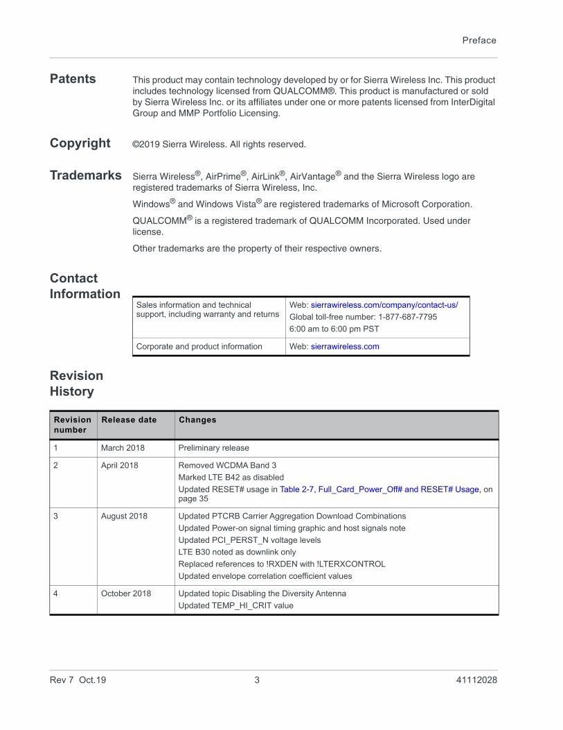
Revision History
Sales information and technical support, including warranty and returns
Web: sierrawireless.com/company/contact-us/
Global toll-free number: 1-877-687-7795
6:00 am to 6:00 pm PST
Corporate and product information Web: sierrawireless.com
Revision number
Release date Changes
1 March 2018 Preliminary release
2 April 2018 Removed WCDMA Band 3
Marked LTE B42 as disabled
Updated RESET# usage in Table 2-7, Full_Card_Power_Off# and RESET# Usage, on page 35
3 August 2018 Updated PTCRB Carrier Aggregation Download Combinations
Updated Power-on signal timing graphic and host signals note
Updated PCI_PERST_N voltage levels
LTE B30 noted as downlink only
Replaced references to !RXDEN with !LTERXCONTROL
Updated envelope correlation coefficient values
4 October 2018 Updated topic Disabling the Diversity Antenna
Updated TEMP_HI_CRIT value
Rev 7 Oct.19 3 41112028
Product Technical Specification
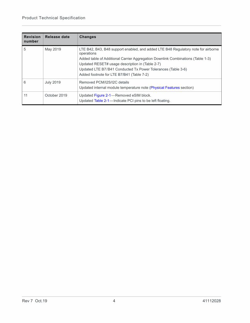
5 May 2019 LTE B42, B43, B48 support enabled, and added LTE B48 Regulatory note for airborne operations
Added table of Additional Carrier Aggregation Downlink Combinations (Table 1-3)
Updated RESET# usage description in (Table 2-7)
Updated LTE B7/B41 Conducted Tx Power Tolerances (Table 3-6)
Added footnote for LTE B7/B41 (Table 7-2)
6 July 2019 Removed PCM/I2S/I2C details
Updated internal module temperature note (Physical Features section)
11 October 2019 Updated Figure 2-1—Removed eSIM block.
Updated Table 2-1—Indicate PCI pins to be left floating.
Revision number
Release date Changes
Rev 7 Oct.19 4 41112028
Re
Contents
Introduction . . . . . . . . . . . . . . . . . . . . . . . . . . . . . . . . . . . . . . . . . . . . . . . . . . . . . . . . . . . .12
Supported RF bands . . . . . . . . . . . . . . . . . . . . . . . . . . . . . . . . . . . . . . . . . . . . . . . . . . 12
Physical Features . . . . . . . . . . . . . . . . . . . . . . . . . . . . . . . . . . . . . . . . . . . . . . . . . . . . . 15
Application Interface Features . . . . . . . . . . . . . . . . . . . . . . . . . . . . . . . . . . . . . . . . . . . 15
Module Features. . . . . . . . . . . . . . . . . . . . . . . . . . . . . . . . . . . . . . . . . . . . . . . . . . . . . . 16
LTE Features . . . . . . . . . . . . . . . . . . . . . . . . . . . . . . . . . . . . . . . . . . . . . . . . . . . . . . . . 16
Short Message Service (SMS) Features . . . . . . . . . . . . . . . . . . . . . . . . . . . . . . . . . . . 17
Position Location (GNSS). . . . . . . . . . . . . . . . . . . . . . . . . . . . . . . . . . . . . . . . . . . . . . . 17
Supporting Documents . . . . . . . . . . . . . . . . . . . . . . . . . . . . . . . . . . . . . . . . . . . . . . . . . 17
Accessories . . . . . . . . . . . . . . . . . . . . . . . . . . . . . . . . . . . . . . . . . . . . . . . . . . . . . . . . . 17
Required Connectors . . . . . . . . . . . . . . . . . . . . . . . . . . . . . . . . . . . . . . . . . . . . . . . . . . 17
Ordering Information. . . . . . . . . . . . . . . . . . . . . . . . . . . . . . . . . . . . . . . . . . . . . . . . . . . 18
Integration Requirements . . . . . . . . . . . . . . . . . . . . . . . . . . . . . . . . . . . . . . . . . . . . . . . 18
Electrical Specifications . . . . . . . . . . . . . . . . . . . . . . . . . . . . . . . . . . . . . . . . . . . . . . . . . .19
Host Interface Pin Assignments . . . . . . . . . . . . . . . . . . . . . . . . . . . . . . . . . . . . . . . . . . 22
Power Supply . . . . . . . . . . . . . . . . . . . . . . . . . . . . . . . . . . . . . . . . . . . . . . . . . . . . . . . . 27
USB Interface . . . . . . . . . . . . . . . . . . . . . . . . . . . . . . . . . . . . . . . . . . . . . . . . . . . . . . . . 28
Host-side Recommendation . . . . . . . . . . . . . . . . . . . . . . . . . . . . . . . . . . . . . . . . . . .28
USB Throughput Performance . . . . . . . . . . . . . . . . . . . . . . . . . . . . . . . . . . . . . . . . .29
User-developed Drivers . . . . . . . . . . . . . . . . . . . . . . . . . . . . . . . . . . . . . . . . . . . . . .29
SIM Interface . . . . . . . . . . . . . . . . . . . . . . . . . . . . . . . . . . . . . . . . . . . . . . . . . . . . . . . . 29
SIM Implementation . . . . . . . . . . . . . . . . . . . . . . . . . . . . . . . . . . . . . . . . . . . . . . . . .31
Control Interface (Signals) . . . . . . . . . . . . . . . . . . . . . . . . . . . . . . . . . . . . . . . . . . . . . . 32
WAKE_ON_WAN# — Wake Host . . . . . . . . . . . . . . . . . . . . . . . . . . . . . . . . . . . . . .32
W_DISABLE# (Wireless Disable) and GPS_DISABLE# (GNSS Disable) . . . . . . . .33
Full_Card_Power_Off# and RESET# . . . . . . . . . . . . . . . . . . . . . . . . . . . . . . . . . . . .34
WWAN_LED#—LED Output . . . . . . . . . . . . . . . . . . . . . . . . . . . . . . . . . . . . . . . . . .35
Antenna Control . . . . . . . . . . . . . . . . . . . . . . . . . . . . . . . . . . . . . . . . . . . . . . . . . . . . . . 36
v 7 Oct.19 5 41112028
Product Technical Specification
RF Specifications . . . . . . . . . . . . . . . . . . . . . . . . . . . . . . . . . . . . . . . . . . . . . . . . . . . . . . . 37
RF Connections . . . . . . . . . . . . . . . . . . . . . . . . . . . . . . . . . . . . . . . . . . . . . . . . . . . . . . 37
Shielding . . . . . . . . . . . . . . . . . . . . . . . . . . . . . . . . . . . . . . . . . . . . . . . . . . . . . . . . . 37
Antenna and Cabling . . . . . . . . . . . . . . . . . . . . . . . . . . . . . . . . . . . . . . . . . . . . . . . . 38
Ground Connection . . . . . . . . . . . . . . . . . . . . . . . . . . . . . . . . . . . . . . . . . . . . . . . . . . . 39
Interference and Sensitivity . . . . . . . . . . . . . . . . . . . . . . . . . . . . . . . . . . . . . . . . . . . . . 39
Interference from Other Wireless Devices . . . . . . . . . . . . . . . . . . . . . . . . . . . . . . . . 39
Host-generated RF Interference . . . . . . . . . . . . . . . . . . . . . . . . . . . . . . . . . . . . . . . 40
Device-generated RF Interference . . . . . . . . . . . . . . . . . . . . . . . . . . . . . . . . . . . . . 40
Methods to Mitigate Decreased Rx Performance . . . . . . . . . . . . . . . . . . . . . . . . . . 40
Radiated Spurious Emissions (RSE) . . . . . . . . . . . . . . . . . . . . . . . . . . . . . . . . . . . . 40
Radiated Sensitivity Measurement . . . . . . . . . . . . . . . . . . . . . . . . . . . . . . . . . . . . . . . 41
Sierra Wireless’ Sensitivity Testing and Desensitization Investigation . . . . . . . . . . 41
Sensitivity vs. Frequency . . . . . . . . . . . . . . . . . . . . . . . . . . . . . . . . . . . . . . . . . . . . . 41
Supported Frequencies . . . . . . . . . . . . . . . . . . . . . . . . . . . . . . . . . . . . . . . . . . . . . . . . 41
Conducted Rx Sensitivity / Tx Power. . . . . . . . . . . . . . . . . . . . . . . . . . . . . . . . . . . . . . 45
GNSS Specifications . . . . . . . . . . . . . . . . . . . . . . . . . . . . . . . . . . . . . . . . . . . . . . . . . . 47
Power . . . . . . . . . . . . . . . . . . . . . . . . . . . . . . . . . . . . . . . . . . . . . . . . . . . . . . . . . . . . . . . . . 48
Power Consumption. . . . . . . . . . . . . . . . . . . . . . . . . . . . . . . . . . . . . . . . . . . . . . . . . . . 48
Module Power States. . . . . . . . . . . . . . . . . . . . . . . . . . . . . . . . . . . . . . . . . . . . . . . . . . 50
Power State Transitions . . . . . . . . . . . . . . . . . . . . . . . . . . . . . . . . . . . . . . . . . . . . . 51
Power Interface . . . . . . . . . . . . . . . . . . . . . . . . . . . . . . . . . . . . . . . . . . . . . . . . . . . . . . 52
Power Ramp-up . . . . . . . . . . . . . . . . . . . . . . . . . . . . . . . . . . . . . . . . . . . . . . . . . . . . 52
Timing . . . . . . . . . . . . . . . . . . . . . . . . . . . . . . . . . . . . . . . . . . . . . . . . . . . . . . . . . . . 53
Power Supply Noise . . . . . . . . . . . . . . . . . . . . . . . . . . . . . . . . . . . . . . . . . . . . . . . . 54
SED (Smart Error Detection) . . . . . . . . . . . . . . . . . . . . . . . . . . . . . . . . . . . . . . . . . . 55
Tx Power Control . . . . . . . . . . . . . . . . . . . . . . . . . . . . . . . . . . . . . . . . . . . . . . . . . . . . . 55
Software Interface . . . . . . . . . . . . . . . . . . . . . . . . . . . . . . . . . . . . . . . . . . . . . . . . . . . . . . 56
Support Tools. . . . . . . . . . . . . . . . . . . . . . . . . . . . . . . . . . . . . . . . . . . . . . . . . . . . . . . . 56
Host Interface. . . . . . . . . . . . . . . . . . . . . . . . . . . . . . . . . . . . . . . . . . . . . . . . . . . . . . . . 56
Rev 7 Oct.19 6 41112028
Contents
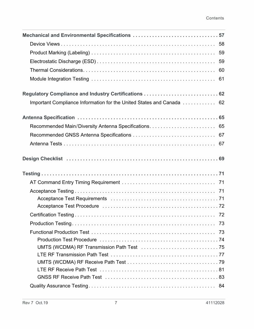
Mechanical and Environmental Specifications . . . . . . . . . . . . . . . . . . . . . . . . . . . . . . . 57
Device Views . . . . . . . . . . . . . . . . . . . . . . . . . . . . . . . . . . . . . . . . . . . . . . . . . . . . . . . . 58
Product Marking (Labeling) . . . . . . . . . . . . . . . . . . . . . . . . . . . . . . . . . . . . . . . . . . . . . 59
Electrostatic Discharge (ESD) . . . . . . . . . . . . . . . . . . . . . . . . . . . . . . . . . . . . . . . . . . . 59
Thermal Considerations. . . . . . . . . . . . . . . . . . . . . . . . . . . . . . . . . . . . . . . . . . . . . . . . 60
Module Integration Testing . . . . . . . . . . . . . . . . . . . . . . . . . . . . . . . . . . . . . . . . . . . . . 61
Regulatory Compliance and Industry Certifications . . . . . . . . . . . . . . . . . . . . . . . . . . . 62
Important Compliance Information for the United States and Canada . . . . . . . . . . . . 62
Antenna Specification . . . . . . . . . . . . . . . . . . . . . . . . . . . . . . . . . . . . . . . . . . . . . . . . . . . 65
Recommended Main/Diversity Antenna Specifications. . . . . . . . . . . . . . . . . . . . . . . . 65
Recommended GNSS Antenna Specifications . . . . . . . . . . . . . . . . . . . . . . . . . . . . . . 67
Antenna Tests . . . . . . . . . . . . . . . . . . . . . . . . . . . . . . . . . . . . . . . . . . . . . . . . . . . . . . . 67
Design Checklist . . . . . . . . . . . . . . . . . . . . . . . . . . . . . . . . . . . . . . . . . . . . . . . . . . . . . . . 69
Testing . . . . . . . . . . . . . . . . . . . . . . . . . . . . . . . . . . . . . . . . . . . . . . . . . . . . . . . . . . . . . . . . 71
AT Command Entry Timing Requirement . . . . . . . . . . . . . . . . . . . . . . . . . . . . . . . . . . 71
Acceptance Testing . . . . . . . . . . . . . . . . . . . . . . . . . . . . . . . . . . . . . . . . . . . . . . . . . . . 71
Acceptance Test Requirements . . . . . . . . . . . . . . . . . . . . . . . . . . . . . . . . . . . . . . . 71
Acceptance Test Procedure . . . . . . . . . . . . . . . . . . . . . . . . . . . . . . . . . . . . . . . . . . 72
Certification Testing . . . . . . . . . . . . . . . . . . . . . . . . . . . . . . . . . . . . . . . . . . . . . . . . . . . 72
Production Testing . . . . . . . . . . . . . . . . . . . . . . . . . . . . . . . . . . . . . . . . . . . . . . . . . . . . 73
Functional Production Test . . . . . . . . . . . . . . . . . . . . . . . . . . . . . . . . . . . . . . . . . . . . . 73
Production Test Procedure . . . . . . . . . . . . . . . . . . . . . . . . . . . . . . . . . . . . . . . . . . . 74
UMTS (WCDMA) RF Transmission Path Test . . . . . . . . . . . . . . . . . . . . . . . . . . . . 75
LTE RF Transmission Path Test . . . . . . . . . . . . . . . . . . . . . . . . . . . . . . . . . . . . . . . 77
UMTS (WCDMA) RF Receive Path Test . . . . . . . . . . . . . . . . . . . . . . . . . . . . . . . . . 79
LTE RF Receive Path Test . . . . . . . . . . . . . . . . . . . . . . . . . . . . . . . . . . . . . . . . . . . 81
GNSS RF Receive Path Test . . . . . . . . . . . . . . . . . . . . . . . . . . . . . . . . . . . . . . . . . 83
Quality Assurance Testing. . . . . . . . . . . . . . . . . . . . . . . . . . . . . . . . . . . . . . . . . . . . . . 84
Rev 7 Oct.19 7 41112028
Product Technical Specification
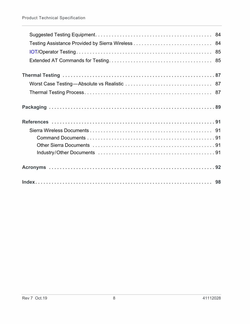
Suggested Testing Equipment. . . . . . . . . . . . . . . . . . . . . . . . . . . . . . . . . . . . . . . . . . . 84
Testing Assistance Provided by Sierra Wireless . . . . . . . . . . . . . . . . . . . . . . . . . . . . . 84
IOT/Operator Testing . . . . . . . . . . . . . . . . . . . . . . . . . . . . . . . . . . . . . . . . . . . . . . . . . . 85
Extended AT Commands for Testing. . . . . . . . . . . . . . . . . . . . . . . . . . . . . . . . . . . . . . 85
Thermal Testing . . . . . . . . . . . . . . . . . . . . . . . . . . . . . . . . . . . . . . . . . . . . . . . . . . . . . . . . 87
Worst Case Testing—Absolute vs Realistic . . . . . . . . . . . . . . . . . . . . . . . . . . . . . . . . 87
Thermal Testing Process. . . . . . . . . . . . . . . . . . . . . . . . . . . . . . . . . . . . . . . . . . . . . . . 87
Packaging . . . . . . . . . . . . . . . . . . . . . . . . . . . . . . . . . . . . . . . . . . . . . . . . . . . . . . . . . . . . . 89
References . . . . . . . . . . . . . . . . . . . . . . . . . . . . . . . . . . . . . . . . . . . . . . . . . . . . . . . . . . . . 91
Sierra Wireless Documents . . . . . . . . . . . . . . . . . . . . . . . . . . . . . . . . . . . . . . . . . . . . . 91
Command Documents . . . . . . . . . . . . . . . . . . . . . . . . . . . . . . . . . . . . . . . . . . . . . . . 91
Other Sierra Documents . . . . . . . . . . . . . . . . . . . . . . . . . . . . . . . . . . . . . . . . . . . . . 91
Industry/Other Documents . . . . . . . . . . . . . . . . . . . . . . . . . . . . . . . . . . . . . . . . . . . 91
Acronyms . . . . . . . . . . . . . . . . . . . . . . . . . . . . . . . . . . . . . . . . . . . . . . . . . . . . . . . . . . . . . 92
Index. . . . . . . . . . . . . . . . . . . . . . . . . . . . . . . . . . . . . . . . . . . . . . . . . . . . . . . . . . . . . . . . . 98
Rev 7 Oct.19 8 41112028
Re
List of Tables
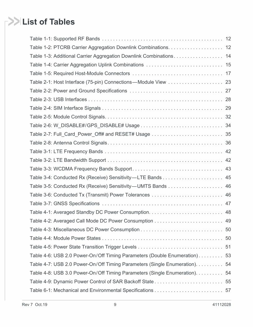
Table 1-1: Supported RF Bands . . . . . . . . . . . . . . . . . . . . . . . . . . . . . . . . . . . . . . . . . . . . 12
Table 1-2: PTCRB Carrier Aggregation Downlink Combinations. . . . . . . . . . . . . . . . . . . . 12
Table 1-3: Additional Carrier Aggregation Downlink Combinations . . . . . . . . . . . . . . . . . . 14
Table 1-4: Carrier Aggregation Uplink Combinations . . . . . . . . . . . . . . . . . . . . . . . . . . . . 15
Table 1-5: Required Host-Module Connectors . . . . . . . . . . . . . . . . . . . . . . . . . . . . . . . . . 17
Table 2-1: Host Interface (75-pin) Connections—Module View . . . . . . . . . . . . . . . . . . . . 23
Table 2-2: Power and Ground Specifications . . . . . . . . . . . . . . . . . . . . . . . . . . . . . . . . . . 27
Table 2-3: USB Interfaces . . . . . . . . . . . . . . . . . . . . . . . . . . . . . . . . . . . . . . . . . . . . . . . . . 28
Table 2-4: SIM Interface Signals . . . . . . . . . . . . . . . . . . . . . . . . . . . . . . . . . . . . . . . . . . . . 29
Table 2-5: Module Control Signals. . . . . . . . . . . . . . . . . . . . . . . . . . . . . . . . . . . . . . . . . . . 32
Table 2-6: W_DISABLE#/GPS_DISABLE# Usage . . . . . . . . . . . . . . . . . . . . . . . . . . . . . . 34
Table 2-7: Full_Card_Power_Off# and RESET# Usage . . . . . . . . . . . . . . . . . . . . . . . . . . 35
Table 2-8: Antenna Control Signals . . . . . . . . . . . . . . . . . . . . . . . . . . . . . . . . . . . . . . . . . . 36
Table 3-1: LTE Frequency Bands . . . . . . . . . . . . . . . . . . . . . . . . . . . . . . . . . . . . . . . . . . . 42
Table 3-2: LTE Bandwidth Support . . . . . . . . . . . . . . . . . . . . . . . . . . . . . . . . . . . . . . . . . . 42
Table 3-3: WCDMA Frequency Bands Support . . . . . . . . . . . . . . . . . . . . . . . . . . . . . . . . . 43
Table 3-4: Conducted Rx (Receive) Sensitivity—LTE Bands . . . . . . . . . . . . . . . . . . . . . . 45
Table 3-5: Conducted Rx (Receive) Sensitivity—UMTS Bands . . . . . . . . . . . . . . . . . . . . 46
Table 3-6: Conducted Tx (Transmit) Power Tolerances . . . . . . . . . . . . . . . . . . . . . . . . . . 46
Table 3-7: GNSS Specifications . . . . . . . . . . . . . . . . . . . . . . . . . . . . . . . . . . . . . . . . . . . . 47
Table 4-1: Averaged Standby DC Power Consumption. . . . . . . . . . . . . . . . . . . . . . . . . . . 48
Table 4-2: Averaged Call Mode DC Power Consumption . . . . . . . . . . . . . . . . . . . . . . . . . 49
Table 4-3: Miscellaneous DC Power Consumption . . . . . . . . . . . . . . . . . . . . . . . . . . . . . . 50
Table 4-4: Module Power States . . . . . . . . . . . . . . . . . . . . . . . . . . . . . . . . . . . . . . . . . . . . 50
Table 4-5: Power State Transition Trigger Levels . . . . . . . . . . . . . . . . . . . . . . . . . . . . . . . 51
Table 4-6: USB 2.0 Power-On/Off Timing Parameters (Double Enumeration) . . . . . . . . . 53
Table 4-7: USB 2.0 Power-On/Off Timing Parameters (Single Enumeration). . . . . . . . . . 54
Table 4-8: USB 3.0 Power-On/Off Timing Parameters (Single Enumeration). . . . . . . . . . 54
Table 4-9: Dynamic Power Control of SAR Backoff State . . . . . . . . . . . . . . . . . . . . . . . . . 55
Table 6-1: Mechanical and Environmental Specifications . . . . . . . . . . . . . . . . . . . . . . . . . 57
v 7 Oct.19 9 41112028
Product Technical Specification
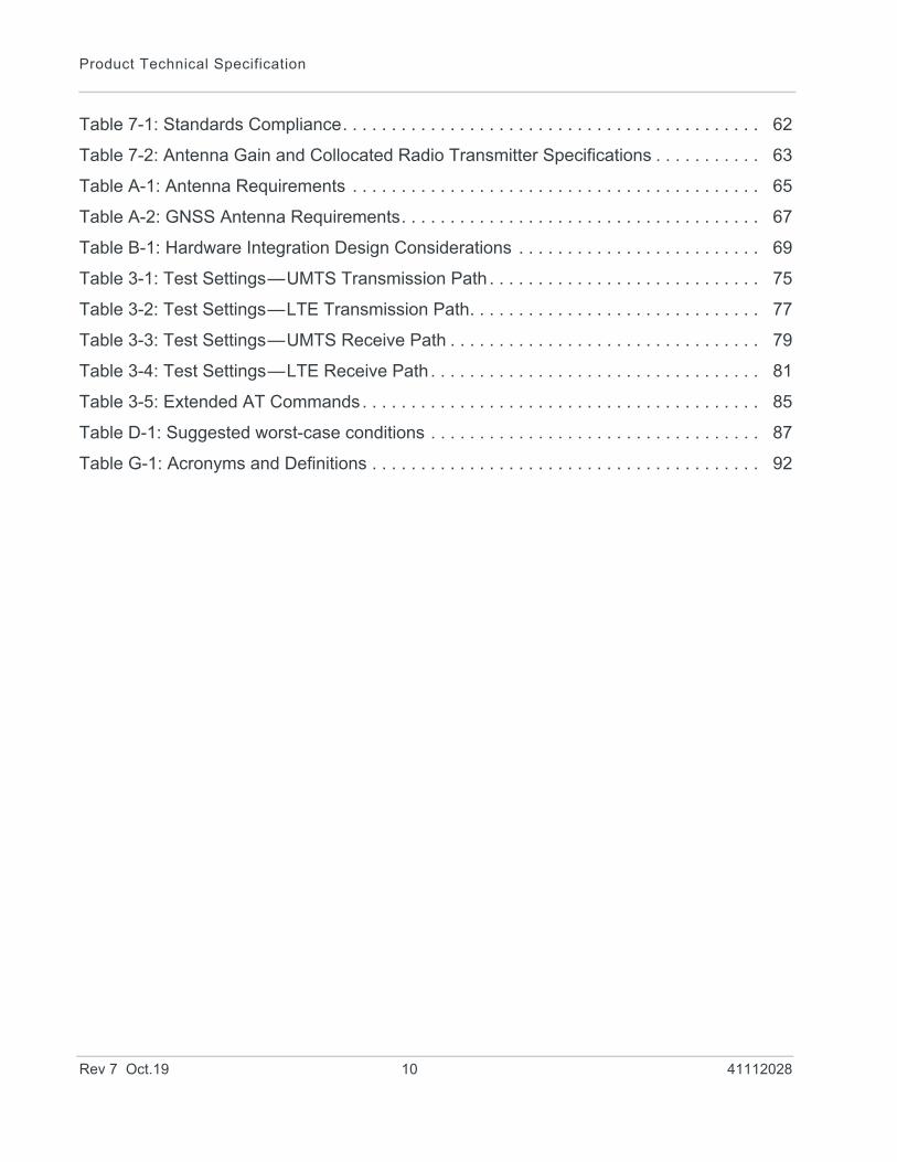
Table 7-1: Standards Compliance. . . . . . . . . . . . . . . . . . . . . . . . . . . . . . . . . . . . . . . . . . . 62
Table 7-2: Antenna Gain and Collocated Radio Transmitter Specifications . . . . . . . . . . . 63
Table A-1: Antenna Requirements . . . . . . . . . . . . . . . . . . . . . . . . . . . . . . . . . . . . . . . . . . 65
Table A-2: GNSS Antenna Requirements. . . . . . . . . . . . . . . . . . . . . . . . . . . . . . . . . . . . . 67
Table B-1: Hardware Integration Design Considerations . . . . . . . . . . . . . . . . . . . . . . . . . 69
Table 3-1: Test Settings—UMTS Transmission Path . . . . . . . . . . . . . . . . . . . . . . . . . . . . 75
Table 3-2: Test Settings—LTE Transmission Path. . . . . . . . . . . . . . . . . . . . . . . . . . . . . . 77
Table 3-3: Test Settings—UMTS Receive Path . . . . . . . . . . . . . . . . . . . . . . . . . . . . . . . . 79
Table 3-4: Test Settings—LTE Receive Path . . . . . . . . . . . . . . . . . . . . . . . . . . . . . . . . . . 81
Table 3-5: Extended AT Commands. . . . . . . . . . . . . . . . . . . . . . . . . . . . . . . . . . . . . . . . . 85
Table D-1: Suggested worst-case conditions . . . . . . . . . . . . . . . . . . . . . . . . . . . . . . . . . . 87
Table G-1: Acronyms and Definitions . . . . . . . . . . . . . . . . . . . . . . . . . . . . . . . . . . . . . . . . 92
Rev 7 Oct.19 10 41112028
Rev 7 Oct.19 11 41112028
List of Figures
Figure 2-1: System Block Diagram . . . . . . . . . . . . . . . . . . . . . . . . . . . . . . . . . . . . . . . . . . 20
Figure 2-2: Expanded RF (Transmit) Block Diagram. . . . . . . . . . . . . . . . . . . . . . . . . . . . . 21
Figure 2-3: Expanded RF (Receive/GNSS) Block Diagram . . . . . . . . . . . . . . . . . . . . . . . 22
Figure 2-4: Recommended Capacitor Placement for USB3.0 Signals . . . . . . . . . . . . . . . 28
Figure 2-5: SIM Application Interface (applies to both SIM interfaces) . . . . . . . . . . . . . . . 30
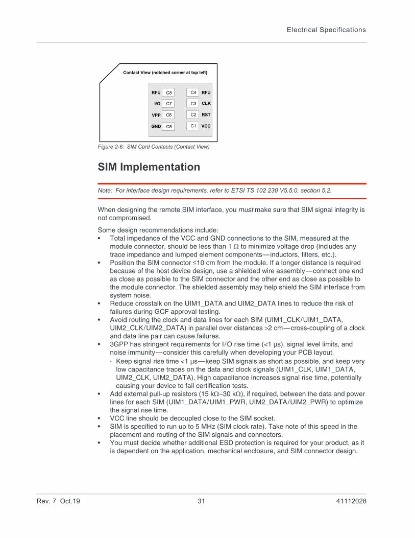
Figure 2-6: SIM Card Contacts (Contact View) . . . . . . . . . . . . . . . . . . . . . . . . . . . . . . . . . 31
Figure 2-7: Recommended WAKE_ON_WAN# Connection . . . . . . . . . . . . . . . . . . . . . . . 33
Figure 2-8: Recommended Wireless Disable Connection . . . . . . . . . . . . . . . . . . . . . . . . . 34
Figure 2-9: Example LED. . . . . . . . . . . . . . . . . . . . . . . . . . . . . . . . . . . . . . . . . . . . . . . . . . 36
Figure 3-1: Module Connectors . . . . . . . . . . . . . . . . . . . . . . . . . . . . . . . . . . . . . . . . . . . . . 37
Figure 4-1: Voltage/Temperature Monitoring State Machines. . . . . . . . . . . . . . . . . . . . . . 52
Figure 4-2: Signal Timing (Full_Card_Power_Off#, and USB Enumeration) . . . . . . . . . . . 53
Figure 6-1: Top View . . . . . . . . . . . . . . . . . . . . . . . . . . . . . . . . . . . . . . . . . . . . . . . . . . . . . 58
Figure 6-2: Dimensioned View. . . . . . . . . . . . . . . . . . . . . . . . . . . . . . . . . . . . . . . . . . . . . . 58
Figure 6-3: Unit Product Marking Example—Laser-etched, Typical Representation (Not to scale. Contents will vary by SKU.) . . . . . . . . . . . . . . . . . . . . . . . . . . . . . . . . . . . . . . . . . . . 59
Figure 6-4: Shield Locations (Top View) . . . . . . . . . . . . . . . . . . . . . . . . . . . . . . . . . . . . . . 60
Figure 6-5: Copper Pad Location on Bottom Side of Module . . . . . . . . . . . . . . . . . . . . . . 60
Figure 5-1: Device Placement in Module Tray. . . . . . . . . . . . . . . . . . . . . . . . . . . . . . . . . . 89
Figure 5-2: Shipping Package . . . . . . . . . . . . . . . . . . . . . . . . . . . . . . . . . . . . . . . . . . . . . . 90
1
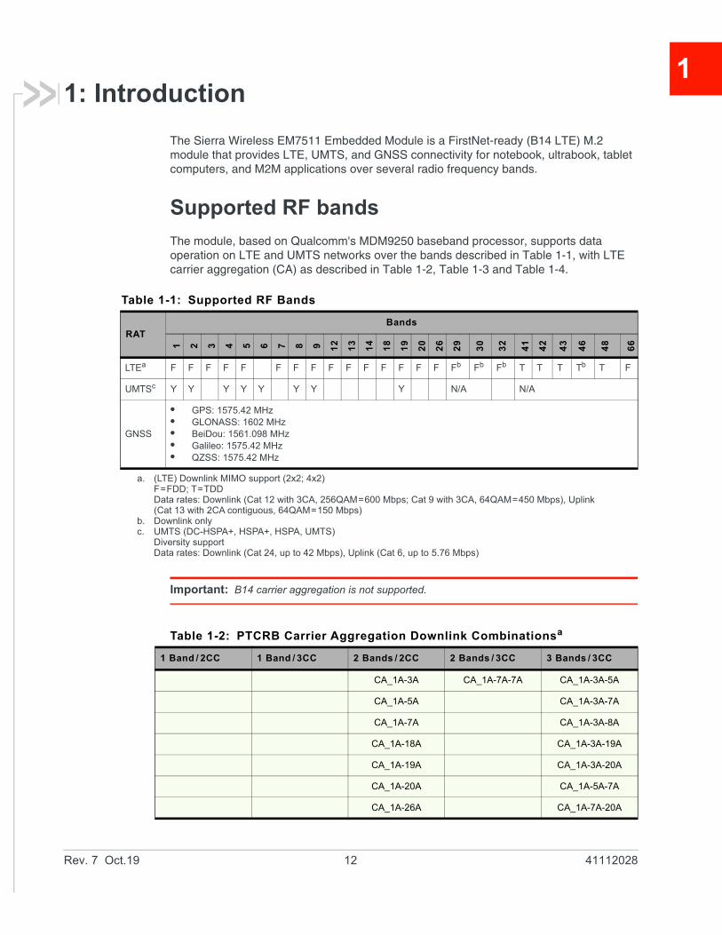
1: IntroductionThe Sierra Wireless EM7511 Embedded Module is a FirstNet-ready (B14 LTE) M.2 module that provides LTE, UMTS, and GNSS connectivity for notebook, ultrabook, tablet computers, and M2M applications over several radio frequency bands.
Supported RF bands
The module, based on Qualcomm's MDM9250 baseband processor, supports data operation on LTE and UMTS networks over the bands described in Table 1-1, with LTE carrier aggregation (CA) as described in Table 1-2, Table 1-3 and Table 1-4.
Important: B14 carrier aggregation is not supported.
Table 1-1: Supported RF Bands
RATBands
1 2 3 4 5 6 7 8 9 12
13
14
18
19
20
26
29
30
32
41
42
43
46
48
66
LTEa F F F F F F F F F F F F F F F Fb Fb Fb T T T Tb T F
UMTSc Y Y Y Y Y Y Y Y N/A N/A
GNSS
• GPS: 1575.42 MHz• GLONASS: 1602 MHz• BeiDou: 1561.098 MHz• Galileo: 1575.42 MHz• QZSS: 1575.42 MHz
a. (LTE) Downlink MIMO support (2x2; 4x2)F=FDD; T=TDDData rates: Downlink (Cat 12 with 3CA, 256QAM=600 Mbps; Cat 9 with 3CA, 64QAM=450 Mbps), Uplink (Cat 13 with 2CA contiguous, 64QAM=150 Mbps)
b. Downlink onlyc. UMTS (DC-HSPA+, HSPA+, HSPA, UMTS)
Diversity supportData rates: Downlink (Cat 24, up to 42 Mbps), Uplink (Cat 6, up to 5.76 Mbps)
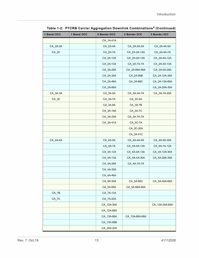
Table 1-2: PTCRB Carrier Aggregation Downlink Combinationsa
1 Band / 2CC 1 Band / 3CC 2 Bands / 2CC 2 Bands / 3CC 3 Bands / 3CC
CA_1A-3A CA_1A-7A-7A CA_1A-3A-5A
CA_1A-5A CA_1A-3A-7A
CA_1A-7A CA_1A-3A-8A
CA_1A-18A CA_1A-3A-19A
CA_1A-19A CA_1A-3A-20A
CA_1A-20A CA_1A-5A-7A
CA_1A-26A CA_1A-7A-20A
Rev. 7 Oct.19 12 41112028
Introduction
CA_1A-41A
CA_2A-2A CA_2A-4A CA_2A-2A-5A CA_2A-4A-5A
CA_2C CA_2A-7A CA_2A-2A-12A CA_2A-4A-7A
CA_2A-12A CA_2A-2A-13A CA_2A-4A-12A
CA_2A-13A CA_2A-7A-7A CA_2A-4A-13A
CA_2A-29A CA_2A-66A-66A CA_2A-4A-29A
CA_2A-30A CA_2A-66B CA_2A-12A-30A
CA_2A-46A CA_2A-66C CA_2A-13A-66A
CA_2A-66A CA_2A-29A-30A
CA_3A-3A CA_3A-5A CA_3A-3A-7A CA_3A-7A-20A
CA_3C CA_3A-7A CA_3C-5A
CA_3A-8A CA_3A-7B
CA_3A-19A CA_3A-7C
CA_3A-20A CA_3A-7A-7A
CA_3A-41A CA_3C-7A
CA_3C-20A
CA_3A-41C
CA_4A-4A CA_4A-5A CA_4A-4A-5A CA_4A-5A-30A
CA_4A-7A CA_4A-4A-12A CA_4A-7A-12A
CA_4A-12A CA_4A-4A-13A CA_4A-12A-30A
CA_4A-13A CA_4A-4A-30A CA_4A-29A-30A
CA_4A-29A CA_4A-7A-7A
CA_4A-30A
CA_4A-46A
CA_5A-30A CA_5A-66C CA_5A-30A-66A
CA_5A-66A CA_5A-66A-66A
CA_7B CA_7A-12A
CA_7C CA_7A-20A
CA_12A-30A CA_12A-30A-66A
CA_12A-66A
CA_13A-66A CA_13A-66A-66A
CA_13A-66B
CA_20A-32A
Table 1-2: PTCRB Carrier Aggregation Downlink Combinationsa (Continued)
1 Band / 2CC 1 Band / 3CC 2 Bands / 2CC 2 Bands / 3CC 3 Bands / 3CC
Rev. 7 Oct.19 13 41112028
Product Technical Specification
CA_29A-30A CA_29A-30A-66A
CA_29A-66A
CA_30A-66A
CA_41D
CA_66B CA_66A-66B
CA_66C CA_66A-66C
a. Supported CA DL combinations outside of North America are carrier-dependent.
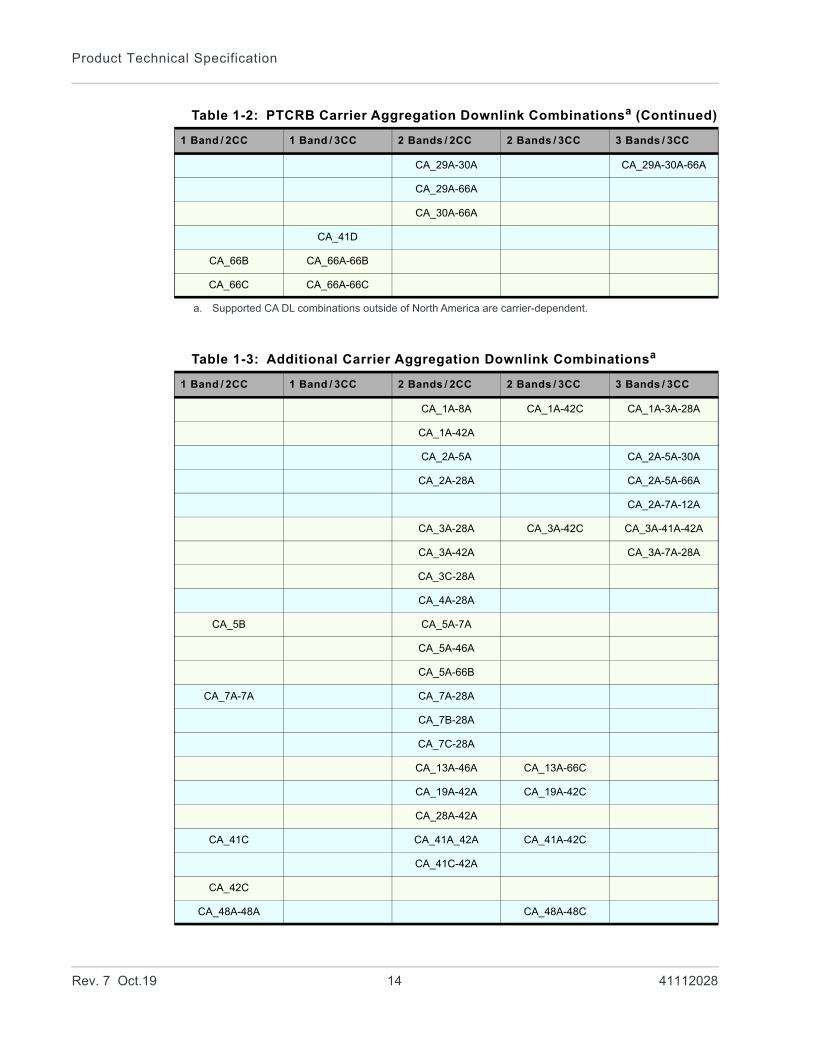
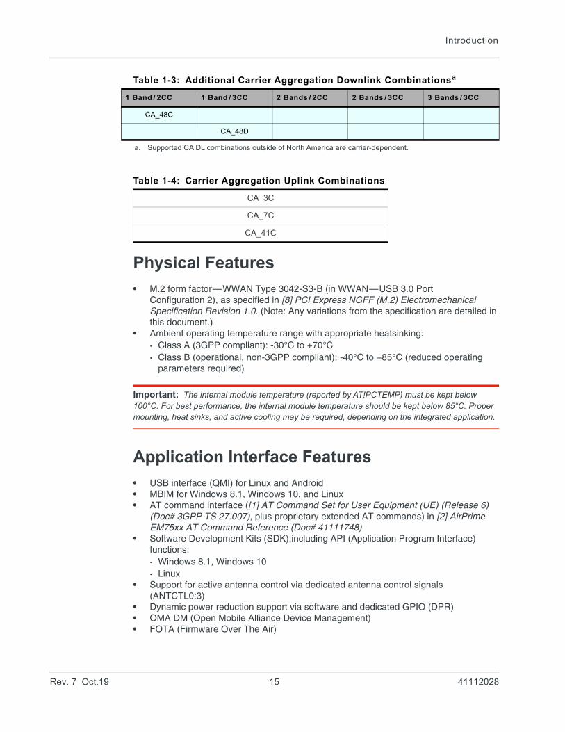
Table 1-3: Additional Carrier Aggregation Downlink Combinationsa
1 Band / 2CC 1 Band / 3CC 2 Bands / 2CC 2 Bands / 3CC 3 Bands / 3CC
CA_1A-8A CA_1A-42C CA_1A-3A-28A
CA_1A-42A
CA_2A-5A CA_2A-5A-30A
CA_2A-28A CA_2A-5A-66A
CA_2A-7A-12A
CA_3A-28A CA_3A-42C CA_3A-41A-42A
CA_3A-42A CA_3A-7A-28A
CA_3C-28A
CA_4A-28A
CA_5B CA_5A-7A
CA_5A-46A
CA_5A-66B
CA_7A-7A CA_7A-28A
CA_7B-28A
CA_7C-28A
CA_13A-46A CA_13A-66C
CA_19A-42A CA_19A-42C
CA_28A-42A
CA_41C CA_41A_42A CA_41A-42C
CA_41C-42A
CA_42C
CA_48A-48A CA_48A-48C
Table 1-2: PTCRB Carrier Aggregation Downlink Combinationsa (Continued)
1 Band / 2CC 1 Band / 3CC 2 Bands / 2CC 2 Bands / 3CC 3 Bands / 3CC
Rev. 7 Oct.19 14 41112028
Introduction
Physical Features
• M.2 form factor—WWAN Type 3042-S3-B (in WWAN—USB 3.0 Port Configuration 2), as specified in [8] PCI Express NGFF (M.2) Electromechanical Specification Revision 1.0. (Note: Any variations from the specification are detailed in this document.)
• Ambient operating temperature range with appropriate heatsinking:· Class A (3GPP compliant): -30°C to +70°C· Class B (operational, non-3GPP compliant): -40°C to +85°C (reduced operating
parameters required)
Important: The internal module temperature (reported by AT!PCTEMP) must be kept below 100°C. For best performance, the internal module temperature should be kept below 85°C. Proper mounting, heat sinks, and active cooling may be required, depending on the integrated application.
Application Interface Features
• USB interface (QMI) for Linux and Android• MBIM for Windows 8.1, Windows 10, and Linux• AT command interface ([1] AT Command Set for User Equipment (UE) (Release 6)
(Doc# 3GPP TS 27.007), plus proprietary extended AT commands) in [2] AirPrime EM75xx AT Command Reference (Doc# 41111748)
• Software Development Kits (SDK),including API (Application Program Interface) functions:· Windows 8.1, Windows 10· Linux
• Support for active antenna control via dedicated antenna control signals (ANTCTL0:3)
• Dynamic power reduction support via software and dedicated GPIO (DPR)• OMA DM (Open Mobile Alliance Device Management)• FOTA (Firmware Over The Air)
CA_48C
CA_48D
a. Supported CA DL combinations outside of North America are carrier-dependent.
Table 1-4: Carrier Aggregation Uplink Combinations
CA_3C
CA_7C
CA_41C
Table 1-3: Additional Carrier Aggregation Downlink Combinationsa
1 Band / 2CC 1 Band / 3CC 2 Bands / 2CC 2 Bands / 3CC 3 Bands / 3CC
Rev. 7 Oct.19 15 41112028
Product Technical Specification
Note: OMA DM and FOTA support is operator-dependent.
Module Features
• LTE / DC-HSPA+ / HSPA+ / HSPA / UMTS (WCDMA) operation• Multiple (up to 16) cellular packet data profiles• Traditional modem COM port support for AT commands• USB suspend / resume• Sleep mode for minimum idle power draw• SIM application tool kit with proactive SIM commands• Enhanced Operator Name String (EONS)• Mobile-originated PDP context activation / deactivation• Support QoS QCI (3GPP Release 12)• Static and Dynamic IP address. The network may assign a fixed IP address or
dynamically assign one using DHCP (Dynamic Host Configuration Protocol).• PAP and CHAP support• PDP context type (IPv4, IPv6, or IPv4v6)• RFC1144 TCP/IP header compression
LTE Features
• Carrier aggregation:· DL LTE-FDD—60 MHz· DL LTE-TDD—60 MHz· UL LTE—40 MHz intraband contiguous
• CSG support (LTE Femto)• LTE Advanced receivers (NLIC, eICIC, feICIC)• Basic cell selection and system acquisition
· PSS/SSS/MIB decode· SIB1–SIB16 decoding
• NAS/AS security procedures· Snow 3G/AES/ZUC security
• CQI/RI/PMI reporting• Paging procedures
· Paging in Idle and Connected mode• Dedicated bearer
· Network-initiated dedicated bearer· UE-initiated dedicated bearer
• Multiple PDN connections (IPv4 and IPv6 combinations), subject to operating system support.
• Connected mode intra-LTE mobility• Idle mode intra-LTE mobility• iRAT between LTE/3G for idle and connection release with redirection• Detach procedure
· Network-initiated detach with reattach required· Network-initiated detach followed by connection release
Rev. 7 Oct.19 16 41112028
Introduction
Short Message Service (SMS) Features
• Mobile-originated and mobile-terminated SMS over IMS• Mobile-originated and mobile-terminated SMS over SGs
Position Location (GNSS)
• Customizable tracking session• Automatic tracking session on startup• Concurrent standalone GPS, GLONASS, Galileo, BeiDou, and QZSS• Assisted GPS (A-GPS) SUPL1.0• Assisted GPS/GLONASS SUPL2.0• gpsOneXTRA 1.0/2.0/3.0/3.1• GNSS reception on dedicated connector or diversity connector
Supporting Documents
Several additional documents describe module design, usage, integration, and other features. See References on page 91.
Accessories
A hardware development kit is available for AirPrime M.2 modules. The kit contains hardware components for evaluating and developing with the module, including:• Development board• Cables• Antennas• Other accessories
For over-the-air LTE testing, ensure that suitable antennas are used.
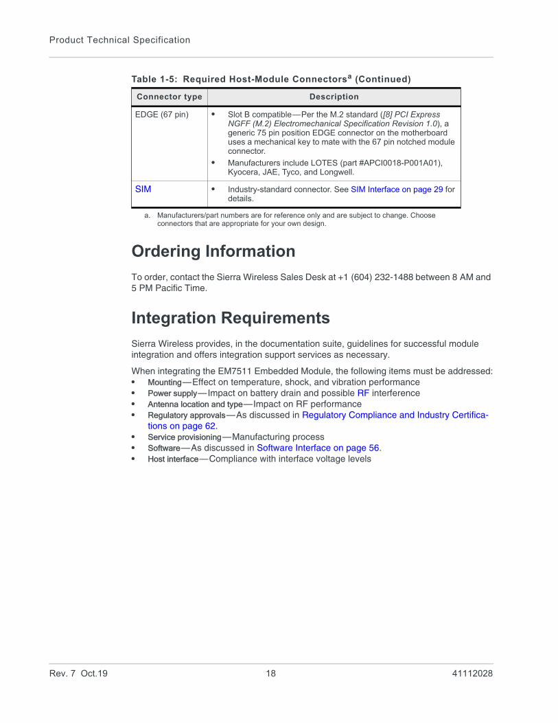
Required ConnectorsTable 1-5 describes the connectors used to integrate the EM7511 Embedded Module into your host device.
Table 1-5: Required Host-Module Connectorsa
Connector type Description
RF cables • Mate with M.2-spec connectors
• Three connector jacks (I-PEX 20448-001R-081 or equivalent)
Rev. 7 Oct.19 17 41112028
Product Technical Specification
Ordering Information
To order, contact the Sierra Wireless Sales Desk at +1 (604) 232-1488 between 8 AM and 5 PM Pacific Time.
Integration Requirements
Sierra Wireless provides, in the documentation suite, guidelines for successful module integration and offers integration support services as necessary.
When integrating the EM7511 Embedded Module, the following items must be addressed:• Mounting—Effect on temperature, shock, and vibration performance• Power supply—Impact on battery drain and possible RF interference• Antenna location and type—Impact on RF performance• Regulatory approvals—As discussed in Regulatory Compliance and Industry Certifica-
tions on page 62.• Service provisioning—Manufacturing process • Software—As discussed in Software Interface on page 56.• Host interface—Compliance with interface voltage levels
EDGE (67 pin) • Slot B compatible—Per the M.2 standard ([8] PCI Express NGFF (M.2) Electromechanical Specification Revision 1.0), a generic 75 pin position EDGE connector on the motherboard uses a mechanical key to mate with the 67 pin notched module connector.
• Manufacturers include LOTES (part #APCI0018-P001A01), Kyocera, JAE, Tyco, and Longwell.
SIM • Industry-standard connector. See SIM Interface on page 29 for details.
a. Manufacturers/part numbers are for reference only and are subject to change. Choose connectors that are appropriate for your own design.
Table 1-5: Required Host-Module Connectorsa (Continued)
Connector type Description
Rev. 7 Oct.19 18 41112028
2
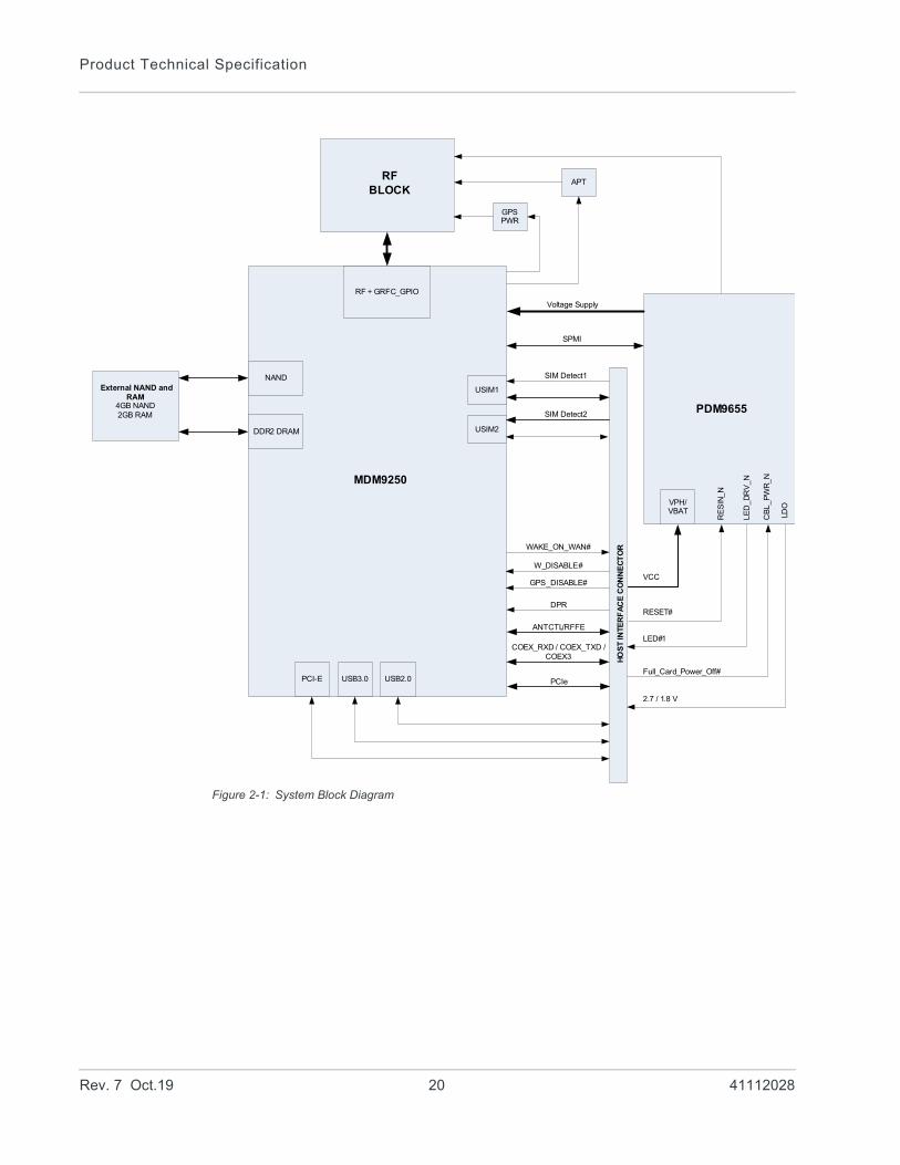
2: Electrical SpecificationsThe system block diagram in Figure 2-1 represents the EM7511 module integrated into a host system. The module includes the following interfaces to the host:• Full_Card_Power_Off#—Input supplied to the module by the host—active-low to turn
the unit off, or active-high to turn the unit on.• W_DISABLE#—Active low input from the host to the EM7511 disables the main RF
radio.• GPS_DISABLE#—Active low input from the host to the EM7511 disables the GNSS
radio receiver.• WAKE_ON_WAN#—Active low output used to wake the host when specific events
occur.• WWAN_LED#—Active-low LED drive signal provides an indication of WAN radio ON
state.• RESET#—Active low input from the host used to reset the module.• Antenna—Three RF connectors (main (Rx/Tx), GNSS, and auxiliary (diversity/MIMO/
GNSS)). For details, see RF Specifications on page 37.• Antenna control—Four signals that can be used to control external antenna switches.• Dynamic power control—Signal used to adjust Tx power to meet FCC SAR require-
ments. For details, see Tx Power Control on page 55.).• Dual SIM—Supported through the interface connector. The SIM cavities / connectors
must be placed on the host device for this feature.• SIM detect—Internal pullup on the module detects whether a SIM is present or not:
· If a SIM is not inserted, the pin must be shorted to ground.· If a SIM is present, the pin will be an open circuit.
• USB—USB 2.0 and USB 3.0 interfaces to the host for data, control, and status infor-mation.
• PCIe port—Reserved for future use.
The EM7511 has two main interface areas—the host I/O connector and the RF ports. Details of these interfaces are described in the sections that follow.
Rev. 7 Oct.19 19 41112028
Product Technical Specification
Figure 2-1: System Block Diagram
External NAND and RAM
4GB NAND2GB RAM
NAND
W_DISABLE#
VCC
PDM9655
USIM1
USB2.0
DPR
VPH/VBAT
CB
L_P
WR
_N
LED
_DR
V_N
LED#1
RF + GRFC_GPIO
RF BLOCK
MDM9250
HO
ST
INTE
RF
AC
E C
ON
NE
CT
OR
GPS_DISABLE#
WAKE_ON_WAN#
Full_Card_Power_Off#
SIM Detect1
ANTCTL/RFFE
RE
SIN
_N
RESET#
DDR2 DRAM
USB3.0
USIM2
SIM Detect2
SPMI
Voltage Supply
PCI-E
LDO
2.7 / 1.8 V
APT
GPS PWR
COEX_RXD / COEX_TXD / COEX3
PCIe
Rev. 7 Oct.19 20 41112028
Electrical Specifications
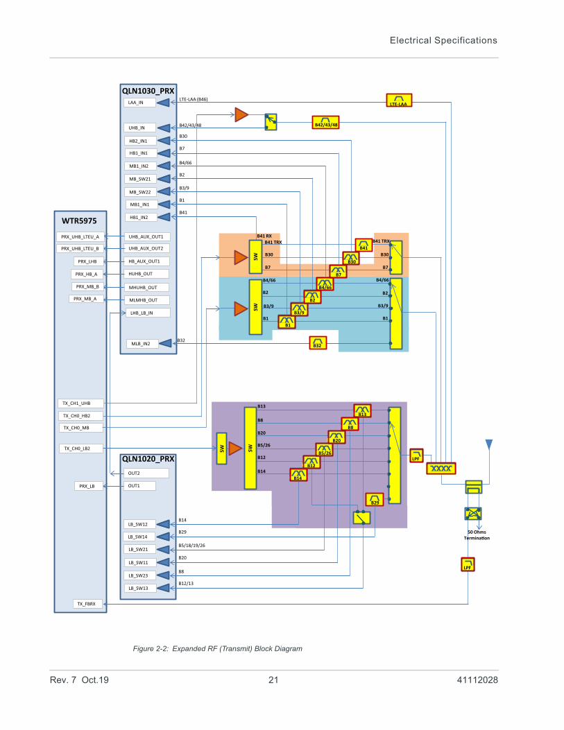
Figure 2-2: Expanded RF (Transmit) Block Diagram
B41 TRX
B30
B7
B4/66
B2
B3/9
B1
SW
B1
B3/9
B2
B4/66
B7
B30
B41 RX
SWB41
B13
B8
B20
B5/26
B12
B14B12
B5/26
B8
B20
B42/43/48
LTE-LAA
B32
OUT2
OUT1
QLN1020_PRX
B5/18/19/26
B20
B29
B14
PRX_LB
LB_SW11
B12/13
B8
UHB_IN
UHB_AUX_OUT1
UHB_AUX_OUT2
HB_AUX_OUT1
HUHB_OUT
QLN1030_PRX
B3/9
B1
B41
B30
B7
B4/66
B2
LTE-LAA (B46)
LHB_LB_IN
MHUHB_OUT
MLMHB_OUT
PRX_UHB_LTEU_A
PRX_UHB_LTEU_B
PRX_LHB
PRX_HB_A
PRX_MB_B
PRX_MB_A
LAA_IN
B42/43/48
HB1_IN2
HB2_IN1
HB1_IN1
MB_SW22
MB1_IN1
MB1_IN2
MB_SW21
MLB_IN2B32
LB_SW21
LB_SW23
LB_SW12
LB_SW14
LB_SW13
TX_CH0_LB2
TX_CH0_MB
TX_CH0_HB2
TX_CH1_UHB
TX_FBRX
WTR5975
B13
SW
B4/66
B2
B3/9
B1
LPF
B29
B14
SW
B41 TRX
B30
B7
LPF
50 OhmsTermina on
Rev. 7 Oct.19 21 41112028
Product Technical Specification
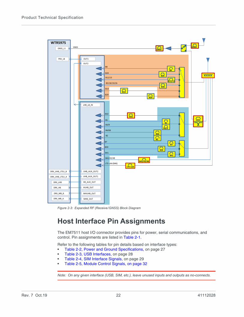
Figure 2-3: Expanded RF (Receive/GNSS) Block Diagram
Host Interface Pin Assignments
The EM7511 host I/O connector provides pins for power, serial communications, and control. Pin assignments are listed in Table 2-1.
Refer to the following tables for pin details based on interface types:• Table 2-2, Power and Ground Specifications, on page 27• Table 2-3, USB Interfaces, on page 28• Table 2-4, SIM Interface Signals, on page 29• Table 2-5, Module Control Signals, on page 32
Note: On any given interface (USB, SIM, etc.), leave unused inputs and outputs as no-connects.
B32
UHB_AUX_OUT2
UHB_AUX_OUT1
HB_AUX_OUT
HUHB_OUT
B41
B42/43/48
LTE-LAA (B46)
B4/66
B2
B7
B30
LHB_LB_IN
MHUHB_OUT
MHB_OUT
DRX_UHB_LTEU_B
DRX_UHB_LTEU_A
DRX_LHB
DRX_HB
DRX_MB_B
DRX_MB_A
B3/9
B1
B66
B2
B1
B3/9
B29
B26
B12/13
B41
B30
B14
GNSSGNSS
GNSS
B7
B42/43/48
B32
GNSS
OUT2
OUT1
B12/13
B29
B8
B20
B14
PRX_LB
B5/18/19/26
WTR5975GNSS_L1
B20
B8
LTE-LAA
Rev. 7 Oct.19 22 41112028
Electrical Specifications
T
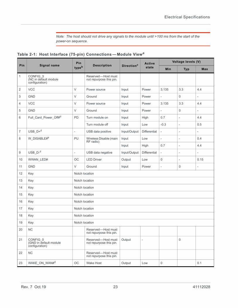
Note: The host should not drive any signals to the module until >100 ms from the start of the power-on sequence.
able 2-1: Host Interface (75-pin) Connections — Module Viewa
Pin Signal namePin
typeb Description Directionc Active state
Voltage levels (V)
Min Typ Max
1 CONFIG_3(NC in default module configuration)
Reserved—Host must not repurpose this pin.
2 VCC V Power source Input Power 3.135 3.3 4.4
3 GND V Ground Input Power - 0 -
4 VCC V Power source Input Power 3.135 3.3 4.4
5 GND V Ground Input Power - 0 -
6 Full_Card_Power_Off#d PD Turn module on Input High 0.7 - 4.4
Turn module off Input Low -0.3 - 0.5
7 USB_D+d - USB data positive Input/Output Differential - - -
8 W_DISABLE#e PU Wireless Disable (main RF radio)
Input Low - - 0.4
Input High 0.7 - 4.4
9 USB_D-d - USB data negative Input/Output Differential - - -
10 WWAN_LED# OC LED Driver Output Low 0 - 0.15
11 GND V Ground Input Power - 0 -
12 Key Notch location
13 Key Notch location
14 Key Notch location
15 Key Notch location
16 Key Notch location
17 Key Notch location
18 Key Notch location
19 Key Notch location
20 NC Reserved—Host must not repurpose this pin.
21 CONFIG_0(GND in default module configuration)
Reserved—Host must not repurpose this pin.
Output - 0
22 NC Reserved—Host must not repurpose this pin.
23 WAKE_ON_WAN#d OC Wake Host Output Low 0 0.1
Rev. 7 Oct.19 23 41112028
Product Technical Specification
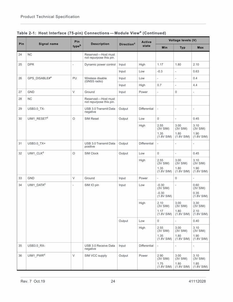
T
24 NC Reserved—Host must not repurpose this pin.
25 DPR - Dynamic power control Input High 1.17 1.80 2.10
Input Low -0.3 - 0.63
26 GPS_DISABLE#e PU Wireless disable (GNSS radio)
Input Low - - 0.4
Input High 0.7 - 4.4
27 GND V Ground Input Power - 0 -
28 NC Reserved—Host must not repurpose this pin.
29 USB3.0_TX- USB 3.0 Transmit Data negative
Output Differential - - -
30 UIM1_RESETd O SIM Reset Output Low 0 - 0.45
High 2.55(3V SIM)
1.35(1.8V SIM)
3.00(3V SIM)
1.80(1.8V SIM)
3.10(3V SIM)
1.90(1.8V SIM)
31 USB3.0_TX+ USB 3.0 Transmit Data positive
Output Differential - - -
32 UIM1_CLKd O SIM Clock Output Low 0 - 0.45
High 2.55(3V SIM)
1.35(1.8V SIM)
3.00(3V SIM)
1.80(1.8V SIM)
3.10(3V SIM)
1.90(1.8V SIM)
33 GND V Ground Input Power - 0 -
34 UIM1_DATAd - SIM IO pin Input Low -0.30(3V SIM)
-0.30(1.8V SIM)
- 0.60(3V SIM)
0.35(1.8V SIM)
High 2.10(3V SIM)
1.17(1.8V SIM)
3.00(3V SIM)
1.80(1.8V SIM)
3.30(3V SIM)
2.10(1.8V SIM)
Output Low 0 - 0.40
High 2.55(3V SIM)
1.35(1.8V SIM)
3.00(3V SIM)
1.80(1.8V SIM)
3.10(3V SIM)
1.90(1.8V SIM)
35 USB3.0_RX- USB 3.0 Receive Data negative
Input Differential - - -
36 UIM1_PWRd V SIM VCC supply Output Power 2.90(3V SIM)
1.75(1.8V SIM)
3.00(3V SIM)
1.80(1.8V SIM)
3.10(3V SIM)
1.85(1.8V SIM)
able 2-1: Host Interface (75-pin) Connections — Module Viewa (Continued)
Pin Signal namePin
typeb Description Directionc Active state
Voltage levels (V)
Min Typ Max
Rev. 7 Oct.19 24 41112028
Electrical Specifications
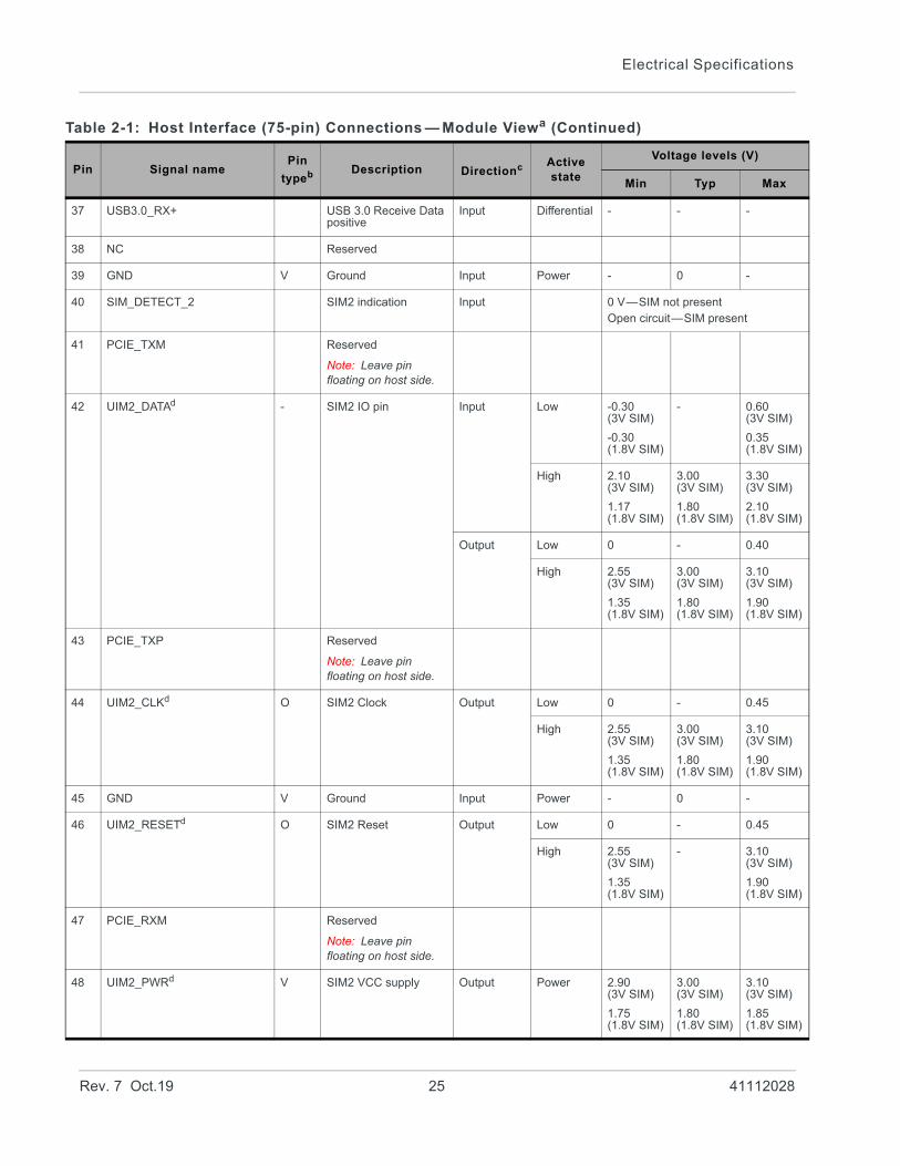
T
37 USB3.0_RX+ USB 3.0 Receive Data positive
Input Differential - - -
38 NC Reserved
39 GND V Ground Input Power - 0 -
40 SIM_DETECT_2 SIM2 indication Input 0 V—SIM not presentOpen circuit—SIM present
41 PCIE_TXM Reserved
Note: Leave pin floating on host side.
42 UIM2_DATAd - SIM2 IO pin Input Low -0.30(3V SIM)
-0.30(1.8V SIM)
- 0.60(3V SIM)
0.35(1.8V SIM)
High 2.10(3V SIM)
1.17(1.8V SIM)
3.00(3V SIM)
1.80(1.8V SIM)
3.30(3V SIM)
2.10(1.8V SIM)
Output Low 0 - 0.40
High 2.55(3V SIM)
1.35(1.8V SIM)
3.00(3V SIM)
1.80(1.8V SIM)
3.10(3V SIM)
1.90(1.8V SIM)
43 PCIE_TXP Reserved
Note: Leave pin floating on host side.
44 UIM2_CLKd O SIM2 Clock Output Low 0 - 0.45
High 2.55(3V SIM)
1.35(1.8V SIM)
3.00(3V SIM)
1.80(1.8V SIM)
3.10(3V SIM)
1.90(1.8V SIM)
45 GND V Ground Input Power - 0 -
46 UIM2_RESETd O SIM2 Reset Output Low 0 - 0.45
High 2.55(3V SIM)
1.35(1.8V SIM)
- 3.10(3V SIM)
1.90(1.8V SIM)
47 PCIE_RXM Reserved
Note: Leave pin floating on host side.
48 UIM2_PWRd V SIM2 VCC supply Output Power 2.90(3V SIM)
1.75(1.8V SIM)
3.00(3V SIM)
1.80(1.8V SIM)
3.10(3V SIM)
1.85(1.8V SIM)
able 2-1: Host Interface (75-pin) Connections — Module Viewa (Continued)
Pin Signal namePin
typeb Description Directionc Active state
Voltage levels (V)
Min Typ Max
Rev. 7 Oct.19 25 41112028
Product Technical Specification
T
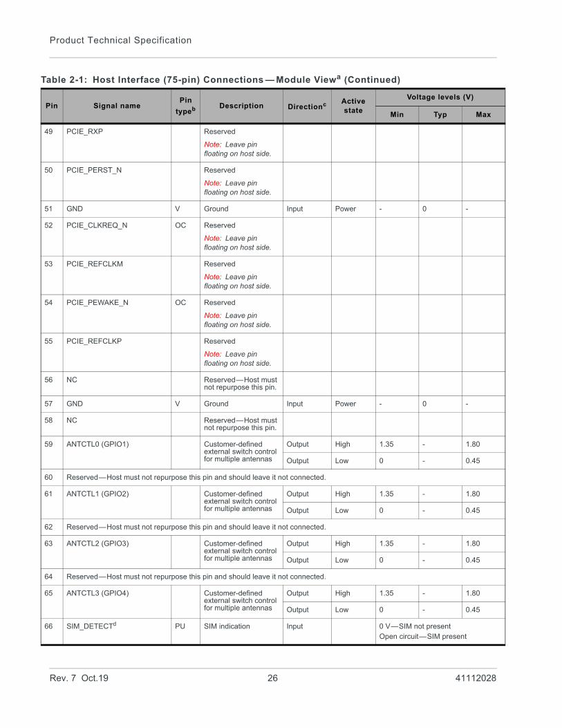
49 PCIE_RXP Reserved
Note: Leave pin floating on host side.
50 PCIE_PERST_N Reserved
Note: Leave pin floating on host side.
51 GND V Ground Input Power - 0 -
52 PCIE_CLKREQ_N OC Reserved
Note: Leave pin floating on host side.
53 PCIE_REFCLKM Reserved
Note: Leave pin floating on host side.
54 PCIE_PEWAKE_N OC Reserved
Note: Leave pin floating on host side.
55 PCIE_REFCLKP Reserved
Note: Leave pin floating on host side.
56 NC Reserved—Host must not repurpose this pin.
57 GND V Ground Input Power - 0 -
58 NC Reserved—Host must not repurpose this pin.
59 ANTCTL0 (GPIO1) Customer-defined external switch control for multiple antennas
Output High 1.35 - 1.80
Output Low 0 - 0.45
60 Reserved—Host must not repurpose this pin and should leave it not connected.
61 ANTCTL1 (GPIO2) Customer-defined external switch control for multiple antennas
Output High 1.35 - 1.80
Output Low 0 - 0.45
62 Reserved—Host must not repurpose this pin and should leave it not connected.
63 ANTCTL2 (GPIO3) Customer-defined external switch control for multiple antennas
Output High 1.35 - 1.80
Output Low 0 - 0.45
64 Reserved—Host must not repurpose this pin and should leave it not connected.
65 ANTCTL3 (GPIO4) Customer-defined external switch control for multiple antennas
Output High 1.35 - 1.80
Output Low 0 - 0.45
66 SIM_DETECTd PU SIM indication Input 0 V—SIM not presentOpen circuit—SIM present
able 2-1: Host Interface (75-pin) Connections — Module Viewa (Continued)
Pin Signal namePin
typeb Description Directionc Active state
Voltage levels (V)
Min Typ Max
Rev. 7 Oct.19 26 41112028
Electrical Specifications
T
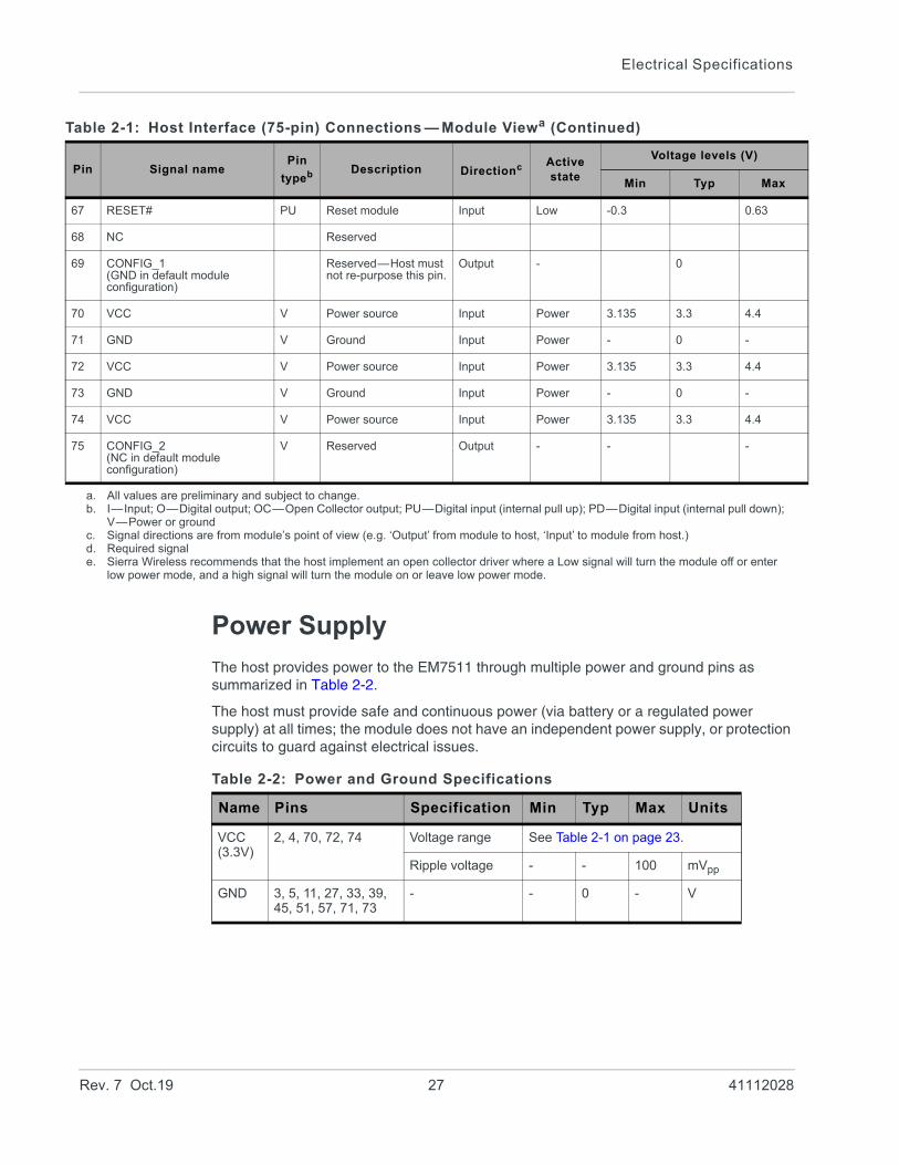
Power Supply
The host provides power to the EM7511 through multiple power and ground pins as summarized in Table 2-2.
The host must provide safe and continuous power (via battery or a regulated power supply) at all times; the module does not have an independent power supply, or protection circuits to guard against electrical issues.
67 RESET# PU Reset module Input Low -0.3 0.63
68 NC Reserved
69 CONFIG_1(GND in default module configuration)
Reserved—Host must not re-purpose this pin.
Output - 0
70 VCC V Power source Input Power 3.135 3.3 4.4
71 GND V Ground Input Power - 0 -
72 VCC V Power source Input Power 3.135 3.3 4.4
73 GND V Ground Input Power - 0 -
74 VCC V Power source Input Power 3.135 3.3 4.4
75 CONFIG_2(NC in default module configuration)
V Reserved Output - - -
a. All values are preliminary and subject to change. b. I—Input; O—Digital output; OC—Open Collector output; PU—Digital input (internal pull up); PD—Digital input (internal pull down);
V—Power or groundc. Signal directions are from module’s point of view (e.g. ‘Output’ from module to host, ‘Input’ to module from host.)d. Required signale. Sierra Wireless recommends that the host implement an open collector driver where a Low signal will turn the module off or enter
low power mode, and a high signal will turn the module on or leave low power mode.
able 2-1: Host Interface (75-pin) Connections — Module Viewa (Continued)
Pin Signal namePin
typeb Description Directionc Active state
Voltage levels (V)
Min Typ Max
Table 2-2: Power and Ground Specifications
Name Pins Specification Min Typ Max Units
VCC(3.3V)
2, 4, 70, 72, 74 Voltage range See Table 2-1 on page 23.
Ripple voltage - - 100 mVpp
GND 3, 5, 11, 27, 33, 39, 45, 51, 57, 71, 73
- - 0 - V
Rev. 7 Oct.19 27 41112028
Product Technical Specification
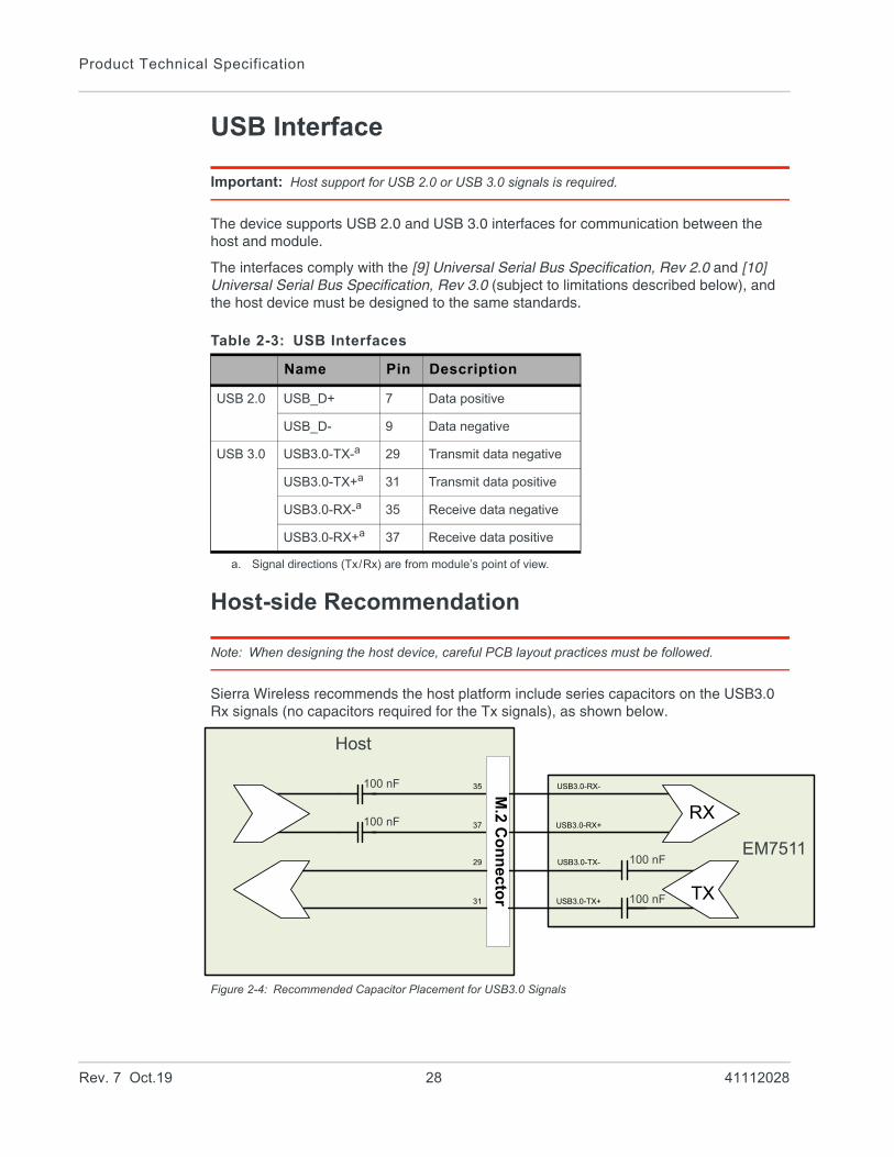
USB Interface
Important: Host support for USB 2.0 or USB 3.0 signals is required.
The device supports USB 2.0 and USB 3.0 interfaces for communication between the host and module.
The interfaces comply with the [9] Universal Serial Bus Specification, Rev 2.0 and [10] Universal Serial Bus Specification, Rev 3.0 (subject to limitations described below), and the host device must be designed to the same standards.
Host-side Recommendation
Note: When designing the host device, careful PCB layout practices must be followed.
Sierra Wireless recommends the host platform include series capacitors on the USB3.0 Rx signals (no capacitors required for the Tx signals), as shown below.
Figure 2-4: Recommended Capacitor Placement for USB3.0 Signals
Table 2-3: USB Interfaces
Name Pin Description
USB 2.0 USB_D+ 7 Data positive
USB_D- 9 Data negative
USB 3.0 USB3.0-TX-a
a. Signal directions (Tx/Rx) are from module’s point of view.
29 Transmit data negative
USB3.0-TX+a 31 Transmit data positive
USB3.0-RX-a 35 Receive data negative
USB3.0-RX+a 37 Receive data positive
M.2 C
on
necto
r
USB3.0-RX-
USB3.0-RX+
USB3.0-TX-
USB3.0-TX+
35
37
29
31
RX
TX
100 nF
100 nF
100 nF
100 nF
Host
EM7511
Rev. 7 Oct.19 28 41112028
Electrical Specifications
USB Throughput Performance
This device has been designed to achieve optimal performance and maximum throughput using USB superspeed mode (USB 3.0). Although the device may operate with a high speed host, throughput performance will be on an “as is” basis and needs to be characterized by the OEM. Note that throughput will be reduced and may vary significantly based on packet size, host interface, and firmware revision.
User-developed Drivers
Details for user-developed USB drivers are described in [4] AirCard/AirPrime USB Driver Developer’s Guide (Doc# 2130634).
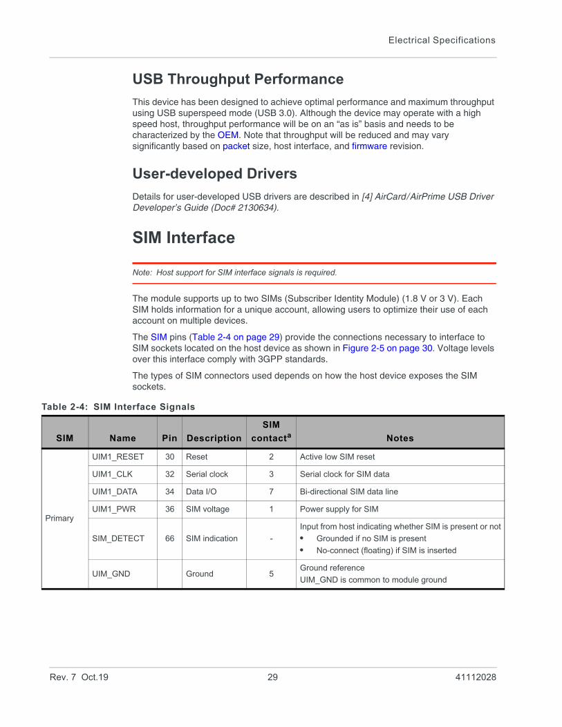
SIM Interface
Note: Host support for SIM interface signals is required.
The module supports up to two SIMs (Subscriber Identity Module) (1.8 V or 3 V). Each SIM holds information for a unique account, allowing users to optimize their use of each account on multiple devices.
The SIM pins (Table 2-4 on page 29) provide the connections necessary to interface to SIM sockets located on the host device as shown in Figure 2-5 on page 30. Voltage levels over this interface comply with 3GPP standards.
The types of SIM connectors used depends on how the host device exposes the SIM sockets.
Table 2-4: SIM Interface Signals
SIM Name Pin Description
SIM
contacta Notes
Primary
UIM1_RESET 30 Reset 2 Active low SIM reset
UIM1_CLK 32 Serial clock 3 Serial clock for SIM data
UIM1_DATA 34 Data I/O 7 Bi-directional SIM data line
UIM1_PWR 36 SIM voltage 1 Power supply for SIM
SIM_DETECT 66 SIM indication -
Input from host indicating whether SIM is present or not
• Grounded if no SIM is present
• No-connect (floating) if SIM is inserted
UIM_GND Ground 5Ground reference
UIM_GND is common to module ground
Rev. 7 Oct.19 29 41112028
Product Technical Specification
Figure 2-5: SIM Application Interface (applies to both SIM interfaces)
Secondary
UIM2_RESET 46 Reset 2 Active low SIM reset
UIM2_CLK 44 Serial clock 3 Serial clock for SIM data
UIM2_DATA 42 Data I/O 7 Bi-directional SIM data line
UIM2_PWR 48 SIM voltage 1 Power supply for SIM
SIM_DETECT_2 40 SIM indication -
Input from host indicating whether SIM is present or not
• Grounded if no SIM is present
• No-connect (floating) if SIM is inserted
UIM2_GND SIM indication -Ground reference
UIM2_GND is common to module ground
a. See Figure 2-6 on page 31 for SIM card contacts.
Table 2-4: SIM Interface Signals (Continued)
SIM Name Pin Description
SIM
contacta Notes
SIM card connector
(Optional. Locate near the
SIM socket)47 pF, 51
4.7uFX5Rtyp
(C1)
UIM-PWR
UIM-CLK
UIM-DATA
UIM-RESET
Located near SIM socket
Located near SIM socket.NOTE: Carefully consider if ESD protection is required – it may increase signal rise time and lead to certification failure
UIM_GND
ESD protection
(C3)
(C7)
(C2)
(C5)
(Optional. Locate near the
SIM socket)15 k - 30 k
0.1uF
SIM Detect
(C9)Note: SIM Detect contact may vary
by vendor
NOTE: UIM signals refer to both UIM1 and UIM2.
EM7511
Rev. 7 Oct.19 30 41112028
Electrical Specifications
Figure 2-6: SIM Card Contacts (Contact View)
SIM Implementation
Note: For interface design requirements, refer to ETSI TS 102 230 V5.5.0, section 5.2.
When designing the remote SIM interface, you must make sure that SIM signal integrity is not compromised.
Some design recommendations include:• Total impedance of the VCC and GND connections to the SIM, measured at the
module connector, should be less than 1 to minimize voltage drop (includes any trace impedance and lumped element components—inductors, filters, etc.).
• Position the SIM connector 10 cm from the module. If a longer distance is required because of the host device design, use a shielded wire assembly—connect one end as close as possible to the SIM connector and the other end as close as possible to the module connector. The shielded assembly may help shield the SIM interface from system noise.
• Reduce crosstalk on the UIM1_DATA and UIM2_DATA lines to reduce the risk of failures during GCF approval testing.
• Avoid routing the clock and data lines for each SIM (UIM1_CLK/UIM1_DATA, UIM2_CLK/UIM2_DATA) in parallel over distances 2 cm—cross-coupling of a clock and data line pair can cause failures.
• 3GPP has stringent requirements for I/O rise time (<1 µs), signal level limits, and noise immunity—consider this carefully when developing your PCB layout.· Keep signal rise time <1 µs—keep SIM signals as short as possible, and keep very
low capacitance traces on the data and clock signals (UIM1_CLK, UIM1_DATA, UIM2_CLK, UIM2_DATA). High capacitance increases signal rise time, potentially causing your device to fail certification tests.
• Add external pull-up resistors (15 k–30 k), if required, between the data and power lines for each SIM (UIM1_DATA/UIM1_PWR, UIM2_DATA/UIM2_PWR) to optimize the signal rise time.
• VCC line should be decoupled close to the SIM socket.• SIM is specified to run up to 5 MHz (SIM clock rate). Take note of this speed in the
placement and routing of the SIM signals and connectors.• You must decide whether additional ESD protection is required for your product, as it
is dependent on the application, mechanical enclosure, and SIM connector design.
C8
C7
C6
C5
C4
C3
C2
C1GND VCC
VPP RST
I/O CLK
RFU RFU
Contact View (notched corner at top left)
Rev. 7 Oct.19 31 41112028
Product Technical Specification
The SIM pins will require additional ESD protection if they are exposed to high ESD levels (i.e. can be touched by a user).
• Putting optional decoupling capacitors on the SIM power lines (UIM1_PWR, UIM2_PWR) near the SIM sockets is recommended—the longer the trace length (impedance) from the socket to the module, the greater the capacitance requirement to meet compliance tests.
• Putting an optional series capacitor and resistor termination (to ground) on the clock lines (UIM1_CLK, UIM2_CLK) at the SIM sockets to reduce EMI and increase signal integrity is recommended if the trace length between the SIM socket and module is long—47 pF and 50 resistor are recommended.
• Test your first prototype host hardware with a Comprion IT3 SIM test device at a suitable testing facility.
Control Interface (Signals)
The EM7511 provides signals for:• Waking the host when specific events occur• Host control of the module’s radios• Host control of module power• LED driver output
Note: Host support for Full_Card_Power_Off# is required, and support for other signals in Table 2-5 is optional.
These signals are summarized in Table 2-5 and paragraphs that follow.
WAKE_ON_WAN# — Wake Host
Note: Host support for WAKE_ON_WAN# is optional.
The EM7511 uses WAKE_ON_WAN# to wake the host when specific events occur.
Table 2-5: Module Control Signals
Name Pin Description Typea
a. O—Digital pin Output; OC—Open Collector output; PD—Digital pin Input, internal pull down; PU—Digital pin Input, internal pull up
Full_Card_Power_Off# 6 On/off signal PD
W_DISABLE# 8 Wireless disable (Main RF) PU
WWAN_LED# 10 LED driver OC
WAKE_ON_WAN# 23 Wake host O
GPS_DISABLE# 26 Wireless disable (GNSS) PU
RESET# 67 Reset module PU
Rev. 7 Oct.19 32 41112028
Electrical Specifications
The host must provide a 5 k–100 k pullup resistor that considers total line capacitance (including parasitic capacitance) such that when WAKE_ON_WAN# is deasserted, the line will rise to 3.3 V (Host power rail) in < 100 ns.
See Figure 2-7 on page 33 for a recommended implementation.
Figure 2-7: Recommended WAKE_ON_WAN# Connection
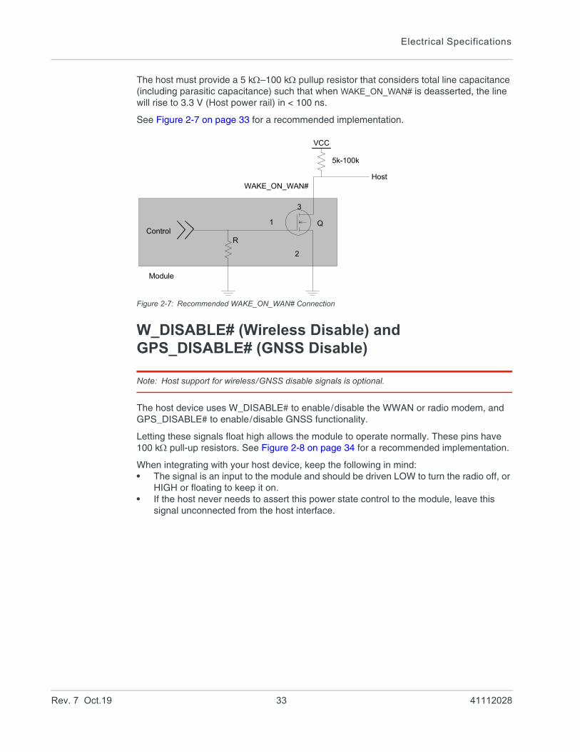
W_DISABLE# (Wireless Disable) and GPS_DISABLE# (GNSS Disable)
Note: Host support for wireless/GNSS disable signals is optional.
The host device uses W_DISABLE# to enable/disable the WWAN or radio modem, and GPS_DISABLE# to enable/disable GNSS functionality.
Letting these signals float high allows the module to operate normally. These pins have 100 k pull-up resistors. See Figure 2-8 on page 34 for a recommended implementation.
When integrating with your host device, keep the following in mind:• The signal is an input to the module and should be driven LOW to turn the radio off, or
HIGH or floating to keep it on.• If the host never needs to assert this power state control to the module, leave this
signal unconnected from the host interface.
ControlR
WAKE_ON_WAN#
1
2
3
Q
5k-100k
Host
VCC
Module
Rev. 7 Oct.19 33 41112028
Product Technical Specification
Figure 2-8: Recommended Wireless Disable Connection
Full_Card_Power_Off# and RESET#
Note: Host support for Full_Card_Power_Off# is required, and support for RESET# is optional.
Full_Card_Power_Off# and RESET# are inputs to the module that the host uses as described in Table 2-7.
For timing details, see Power On/Off Timing for the USB on page 53.
Table 2-6: W_DISABLE# / GPS_DISABLE# Usage
Name Pin Description / notes
W_DISABLE# 8 Enable/disable the WWAN or radio modema. When disabled, the modem cannot transmit or receive.
• Leave as not connected or drive HIGH to keep the modem always on.
• Drive LOW to turn the modem off.
GPS_DISABLE# 26 Enable/disable GNSS functionalitya
• Leave as not connected or drive HIGH to enable GNSS functionality.
• Drive LOW to disable GNSS functionality.
• For details on enabling / disabling GNSS functionality, see the AT!CUSTOM=”GPSENABLE” command in [2] AirPrime EM75xx AT Command Reference (Doc# 41111748).
a. Sierra Wireless recommends that the host implement an open collector driver where a Low signal turns off the modem or dis-ables GNSS functionality, and a high signal turns on the modem or lenables GNSS functionality.
Module
R
Wireless disable control 1
2
3
Q
100k
Host
VCC PMIC for W_DISABLE#
10k
Rev. 7 Oct.19 34 41112028
Electrical Specifications
T
WWAN_LED#—LED Output
Note: Host support for WWAN_LED# is optional.
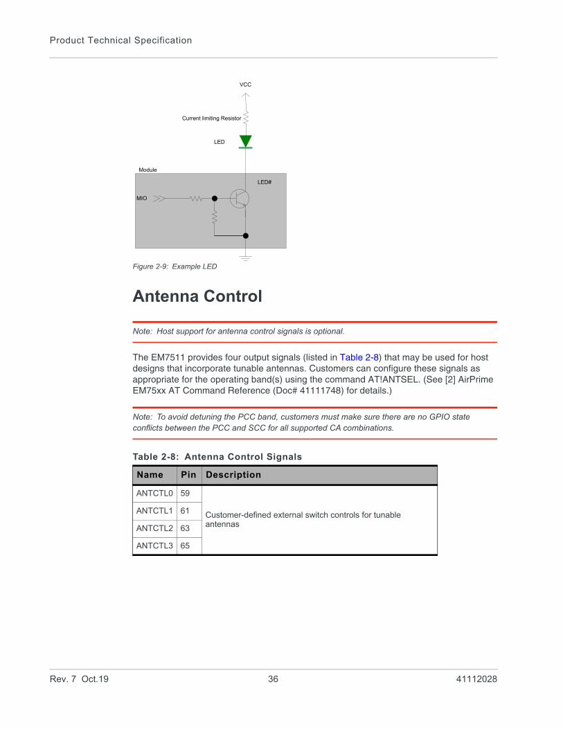
The configuration for the LED shown in Figure 2-9 is customizable. Contact your Sierra Wireless account representative for details.
able 2-7: Full_Card_Power_Off# and RESET# Usage
Name Pin Description / notes
Full_Card_Power_Off# 6 Powers the module on/off.
• Signal is required.
• Pull HIGH to keep the module on. To keep the module always on:
· Tie the pin directly to a host GPIO (1.8V), or· Use an external pull-up to pull signal high (10k–20k for 1.8V, 75–100k for VCC
rail). Note that a larger-value resistor will reduce leakage current.
• To power off the module, see Required Shutdown Sequence on page 54.
RESET# 67 Resets the module.
• Signal is optional. The module will operate correctly if the pin is left disconnected on the host.
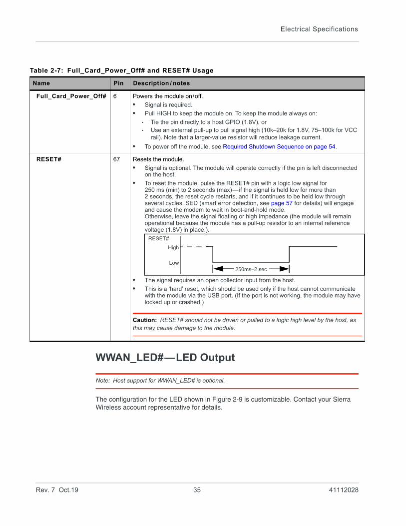
• To reset the module, pulse the RESET# pin with a logic low signal for 250 ms (min) to 2 seconds (max)—if the signal is held low for more than 2 seconds, the reset cycle restarts, and if it continues to be held low through several cycles, SED (smart error detection, see page 57 for details) will engage and cause the modem to wait in boot-and-hold mode. Otherwise, leave the signal floating or high impedance (the module will remain operational because the module has a pull-up resistor to an internal reference voltage (1.8V) in place.).
• The signal requires an open collector input from the host.
• This is a ‘hard’ reset, which should be used only if the host cannot communicate with the module via the USB port. (If the port is not working, the module may have locked up or crashed.)
Caution: RESET# should not be driven or pulled to a logic high level by the host, as this may cause damage to the module.
RESET#
250ms–2 sec
High
Low
Rev. 7 Oct.19 35 41112028
Product Technical Specification
Figure 2-9: Example LED
Antenna Control
Note: Host support for antenna control signals is optional.
The EM7511 provides four output signals (listed in Table 2-8) that may be used for host designs that incorporate tunable antennas. Customers can configure these signals as appropriate for the operating band(s) using the command AT!ANTSEL. (See [2] AirPrime EM75xx AT Command Reference (Doc# 41111748) for details.)
Note: To avoid detuning the PCC band, customers must make sure there are no GPIO state conflicts between the PCC and SCC for all supported CA combinations.
Table 2-8: Antenna Control Signals
Name Pin Description
ANTCTL0 59
Customer-defined external switch controls for tunable antennas
ANTCTL1 61
ANTCTL2 63
ANTCTL3 65
Current limiting Resistor
LED
VCC
MIO
Module
LED#
Rev. 7 Oct.19 36 41112028
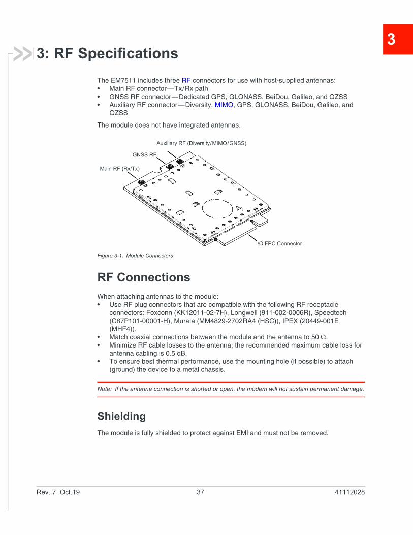
3
3: RF SpecificationsThe EM7511 includes three RF connectors for use with host-supplied antennas:• Main RF connector—Tx/Rx path• GNSS RF connector—Dedicated GPS, GLONASS, BeiDou, Galileo, and QZSS• Auxiliary RF connector—Diversity, MIMO, GPS, GLONASS, BeiDou, Galileo, and
QZSS
The module does not have integrated antennas.
Figure 3-1: Module Connectors
RF Connections
When attaching antennas to the module:• Use RF plug connectors that are compatible with the following RF receptacle
connectors: Foxconn (KK12011-02-7H), Longwell (911-002-0006R), Speedtech (C87P101-00001-H), Murata (MM4829-2702RA4 (HSC)), IPEX (20449-001E (MHF4)).
• Match coaxial connections between the module and the antenna to 50 .• Minimize RF cable losses to the antenna; the recommended maximum cable loss for
antenna cabling is 0.5 dB.• To ensure best thermal performance, use the mounting hole (if possible) to attach
(ground) the device to a metal chassis.
Note: If the antenna connection is shorted or open, the modem will not sustain permanent damage.
Shielding
The module is fully shielded to protect against EMI and must not be removed.
I/O FPC Connector
Main RF (Rx/Tx)
GNSS RF
Auxiliary RF (Diversity/MIMO/GNSS)
Rev. 7 Oct.19 37 41112028
Product Technical Specification
Antenna and Cabling
When selecting the antenna and cable, it is critical to RF performance to match antenna gain and cable loss.
Note: For detailed electrical performance criteria, see Appendix A: Antenna Specification on page 65.
Choosing the Correct Antenna and Cabling
When matching antennas and cabling:• The antenna (and associated circuitry) should have a nominal impedance of 50
with a return loss of better than 10 dB across each frequency band of operation.• The system gain value affects both radiated power and regulatory (FCC, IC, CE, etc.)
test results.
Designing Custom Antennas
Consider the following points when designing custom antennas:• A skilled RF engineer should do the development to ensure that the RF performance
is maintained.• If both UMTS and CDMA modules will be installed in the same platform, you may
want to develop separate antennas for maximum performance.
Determining the Antenna’s Location
When deciding where to put the antennas:• Antenna location may affect RF performance. Although the module is shielded to
prevent interference in most applications, the placement of the antenna is still very important—if the host device is insufficiently shielded, high levels of broadband or spurious noise can degrade the module’s performance.
• Connecting cables between the module and the antenna must have 50 impedance. If the impedance of the module is mismatched, RF performance is reduced signifi-cantly.
• Antenna cables should be routed, if possible, away from noise sources (switching power supplies, LCD assemblies, etc.). If the cables are near the noise sources, the noise may be coupled into the RF cable and into the antenna. See Interference from Other Wireless Devices on page 39.
Disabling the Diversity Antenna
Certification testing of a device with an integrated EM7511 may require the module’s main and diversity antennas to be tested separately.
To facilitate this testing, receive diversity can be enabled/disabled using AT commands:• !RXDEN—Used to enable/disable diversity for single-cell call (no carrier aggre-
gation).• !LTERXCONTROL—Used to enable/disable paths (in carrier aggregation scenarios)
after a call is set up.
Rev. 7 Oct.19 38 41112028
RF Specifications
Important: LTE networks expect modules to have more than one antenna enabled for proper operation. Therefore, customers must not commercially deploy their systems with the diversity antenna disabled.
For details, see [2] AirPrime EM75xx AT Command Reference (Doc# 41111748).
Note: A diversity antenna is used to improve connection quality and reliability through redundancy. Because two antennas may experience difference interference effects (signal distortion, delay, etc.), when one antenna receives a degraded signal, the other may not be similarly affected.
Ground ConnectionWhen connecting the module to system ground:• Prevent noise leakage by establishing a very good ground connection to the module
through the host connector.• Connect to system ground using the mounting hole shown in Figure 3-1 on page 37.• Minimize ground noise leakage into the RF.
Depending on the host board design, noise could potentially be coupled to the module from the host board. This is mainly an issue for host designs that have signals traveling along the length of the module, or circuitry operating at both ends of the module interconnects.
Interference and Sensitivity
Several interference sources can affect the module’s RF performance (RF desense). Common sources include power supply noise and device-generated RF.
RF desense can be addressed through a combination of mitigation techniques (Methods to Mitigate Decreased Rx Performance on page 40) and radiated sensitivity measurement (Radiated Sensitivity Measurement on page 41).
Note: The EM7511 is based on ZIF (Zero Intermediate Frequency) technologies. When performing EMC (Electromagnetic Compatibility) tests, there are no IF (Intermediate Frequency) components from the module to consider.
Interference from Other Wireless Devices
Wireless devices operating inside the host device can cause interference that affects the module.
To determine the most suitable locations for antennas on your host device, evaluate each wireless device’s radio system, considering the following:• Any harmonics, sub-harmonics, or cross-products of signals generated by wireless
devices that fall in the module’s Rx range may cause spurious response, resulting in decreased Rx performance.
• The Tx power and corresponding broadband noise of other wireless devices may overload or increase the noise floor of the module’s receiver, resulting in Rx desense.
Rev. 7 Oct.19 39 41112028
Product Technical Specification
The severity of this interference depends on the closeness of the other antennas to the module’s antenna. To determine suitable locations for each wireless device’s antenna, thoroughly evaluate your host device’s design.
Host-generated RF Interference
All electronic computing devices generate RF interference that can negatively affect the receive sensitivity of the module.
Proximity of host electronics to the antenna in wireless devices can contribute to decreased Rx performance. Components that are most likely to cause this include:• Microprocessor and memory• Display panel and display drivers• Switching-mode power supplies
Device-generated RF Interference
The module can cause interference with other devices. Wireless devices such as AirPrime embedded modules transmit in bursts (pulse transients) for set durations (RF burst frequencies). Hearing aids and speakers convert these burst frequencies into audible frequencies, resulting in audible noise.
Methods to Mitigate Decreased Rx Performance
It is important to investigate sources of localized interference early in the design cycle. To reduce the effect of device-generated RF on Rx performance:• Put the antenna as far as possible from sources of interference. The drawback is that
the module may be less convenient to use.• Shield the host device. The module itself is well shielded to avoid external inter-
ference. However, the antenna cannot be shielded for obvious reasons. In most instances, it is necessary to employ shielding on the components of the host device (such as the main processor and parallel bus) that have the highest RF emissions.
• Filter out unwanted high-order harmonic energy by using discrete filtering on low frequency lines.
• Form shielding layers around high-speed clock traces by using multi-layer PCBs.• Route antenna cables away from noise sources.
Radiated Spurious Emissions (RSE)
When designing an antenna for use with AirPrime embedded modules, the host device with an AirPrime embedded module must satisfy any applicable standards/local regulatory bodies for radiated spurious emission (RSE) for receive-only mode and for transmit mode (transmitter is operating).
Note that antenna impedance affects radiated emissions, which must be compared against the conducted 50-ohm emissions baseline. (AirPrime embedded modules meet the 50-ohm conducted emissions requirement.)
Rev. 7 Oct.19 40 41112028
RF Specifications
Radiated Sensitivity Measurement
A wireless host device contains many noise sources that contribute to a reduction in Rx performance.
To determine the extent of any receiver performance desensitization due to self-generated noise in the host device, over-the-air (OTA) or radiated testing is required. This testing can be performed by Sierra Wireless or you can use your own OTA test chamber for in-house testing.
Sierra Wireless’ Sensitivity Testing and Desensitization Investigation
Although AirPrime embedded modules are designed to meet network operator requirements for receiver performance, they are still susceptible to various performance inhibitors.
As part of the Engineering Services package, Sierra Wireless offers modem OTA sensitivity testing and desensitization (desense) investigation. For more information, contact your account manager or the Sales Desk (see Contact Information on page 3).
Note: Sierra Wireless has the capability to measure TIS (Total Isotropic Sensitivity) and TRP (Total Radiated Power) according to CTIA's published test procedure.
Sensitivity vs. Frequency
For UMTS bands, sensitivity is defined as the input power level in dBm that produces a BER (Bit Error Rate) of 0.1%. Sensitivity should be measured at all UMTS frequencies across each band.
For LTE bands, sensitivity is defined as the RF level at which throughput is 95% of maximum.
Supported Frequencies
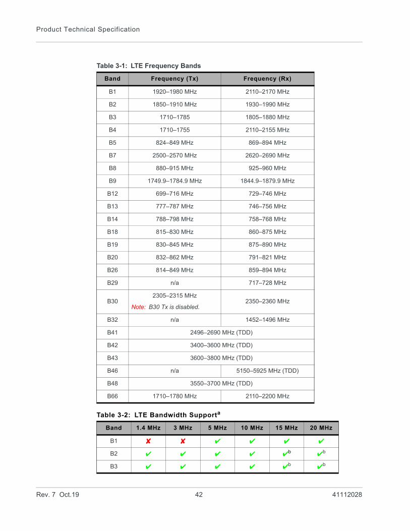
The EM7511 supports:• Multiple-band LTE—See Table 3-1 on page 42 (supported bands) and Table 3-2 on
page 42 (LTE bandwidth support).• LTE Advanced carrier aggregation—See Table 1-1 on page 12, Table 1-2 on
page 12, and Table 1-3 on page 14 for details.• Multiple-band WCDMA/HSPA/HSPA+/DC-HSPA+—See Table 3-3 on page 43.• Multiple-band WCDMA receive diversity• GPS, GLONASS, BeiDou, Galileo, QZSS—See Table 3-7 on page 47.• Inter-RAT and inter-frequency cell reselection and handover between supported
frequency bands
Rev. 7 Oct.19 41 41112028
Product Technical Specification
Table 3-1: LTE Frequency Bands
Band Frequency (Tx) Frequency (Rx)
B1 1920–1980 MHz 2110–2170 MHz
B2 1850–1910 MHz 1930–1990 MHz
B3 1710–1785 1805–1880 MHz
B4 1710–1755 2110–2155 MHz
B5 824–849 MHz 869–894 MHz
B7 2500–2570 MHz 2620–2690 MHz
B8 880–915 MHz 925–960 MHz
B9 1749.9–1784.9 MHz 1844.9–1879.9 MHz
B12 699–716 MHz 729–746 MHz
B13 777–787 MHz 746–756 MHz
B14 788–798 MHz 758–768 MHz
B18 815–830 MHz 860–875 MHz
B19 830–845 MHz 875–890 MHz
B20 832–862 MHz 791–821 MHz
B26 814–849 MHz 859–894 MHz
B29 n/a 717–728 MHz
B302305–2315 MHz
Note: B30 Tx is disabled.2350–2360 MHz
B32 n/a 1452–1496 MHz
B41 2496–2690 MHz (TDD)
B42 3400–3600 MHz (TDD)
B43 3600–3800 MHz (TDD)
B46 n/a 5150–5925 MHz (TDD)
B48 3550–3700 MHz (TDD)
B66 1710–1780 MHz 2110–2200 MHz
Table 3-2: LTE Bandwidth Supporta
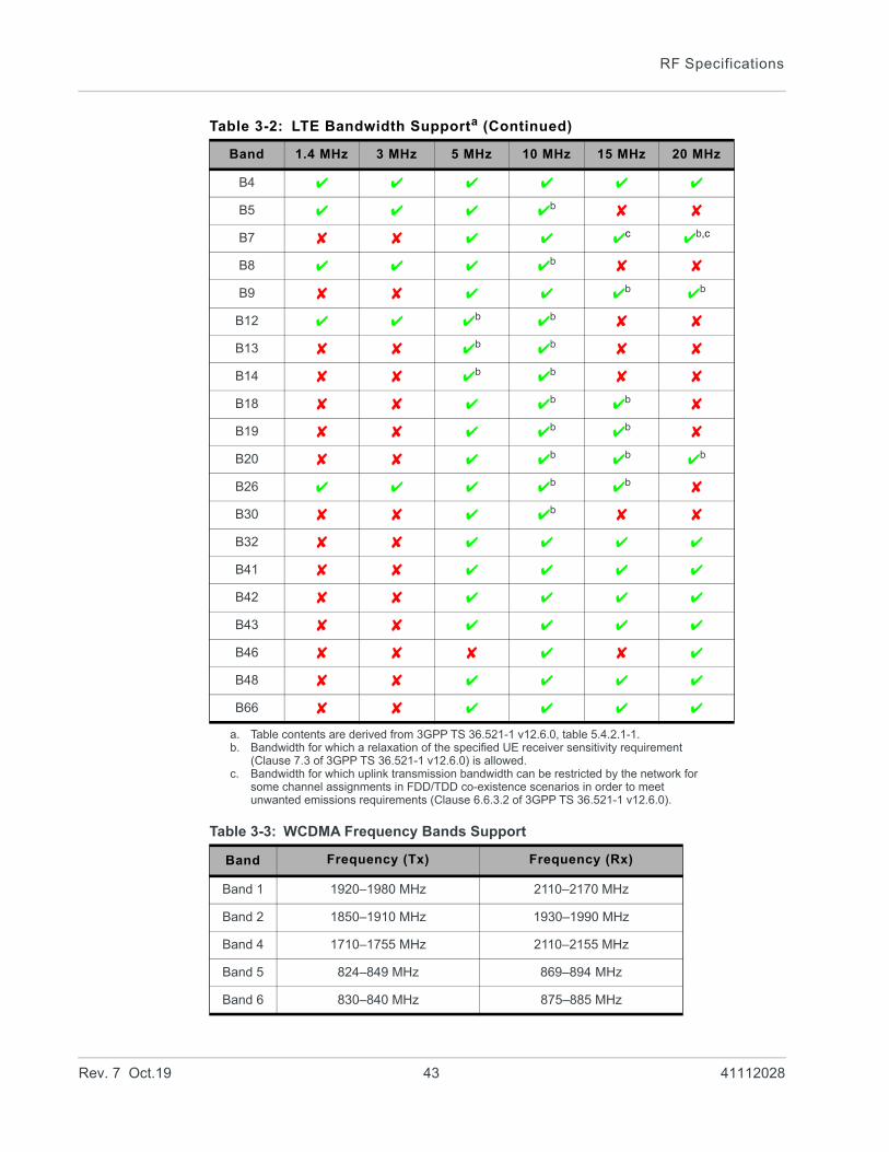
Band 1.4 MHz 3 MHz 5 MHz 10 MHz 15 MHz 20 MHz
B1
B2 b b
B3 b b
Rev. 7 Oct.19 42 41112028
RF Specifications
B4
B5 b
B7 c b,c
B8 b
B9 b b
B12 b b
B13 b b
B14 b b
B18 b b
B19 b b
B20 b b b
B26 b b
B30 b
B32
B41
B42
B43
B46
B48
B66
a. Table contents are derived from 3GPP TS 36.521-1 v12.6.0, table 5.4.2.1-1.b. Bandwidth for which a relaxation of the specified UE receiver sensitivity requirement
(Clause 7.3 of 3GPP TS 36.521-1 v12.6.0) is allowed.c. Bandwidth for which uplink transmission bandwidth can be restricted by the network for
some channel assignments in FDD/TDD co-existence scenarios in order to meet unwanted emissions requirements (Clause 6.6.3.2 of 3GPP TS 36.521-1 v12.6.0).
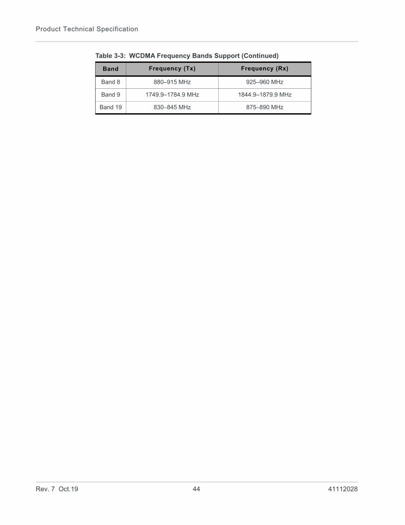
Table 3-3: WCDMA Frequency Bands Support
Band Frequency (Tx) Frequency (Rx)
Band 1 1920–1980 MHz 2110–2170 MHz
Band 2 1850–1910 MHz 1930–1990 MHz
Band 4 1710–1755 MHz 2110–2155 MHz
Band 5 824–849 MHz 869–894 MHz
Band 6 830–840 MHz 875–885 MHz
Table 3-2: LTE Bandwidth Supporta (Continued)
Band 1.4 MHz 3 MHz 5 MHz 10 MHz 15 MHz 20 MHz
Rev. 7 Oct.19 43 41112028
Product Technical Specification
Band 8 880–915 MHz 925–960 MHz
Band 9 1749.9–1784.9 MHz 1844.9–1879.9 MHz
Band 19 830–845 MHz 875–890 MHz
Table 3-3: WCDMA Frequency Bands Support (Continued)
Band Frequency (Tx) Frequency (Rx)
Rev. 7 Oct.19 44 41112028
RF Specifications
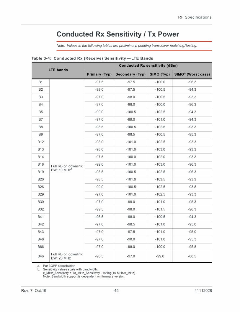
Conducted Rx Sensitivity / Tx Power
Note: Values in the following tables are preliminary, pending transceiver matching/testing.
Table 3-4: Conducted Rx (Receive) Sensitivity — LTE Bands
LTE bandsConducted Rx sensitivity (dBm)
Primary (Typ) Secondary (Typ) SIMO (Typ) SIMOa (Worst case)
B1
Full RB on downlink;BW: 10 MHzb
-97.5 -97.5 -100.0 -96.3
B2 -98.0 -97.5 -100.5 -94.3
B3 -97.0 -98.0 -100.5 -93.3
B4 -97.0 -98.0 -100.0 -96.3
B5 -99.0 -100.5 -102.5 -94.3
B7 -97.0 -99.0 -101.0 -94.3
B8 -98.5 -100.5 -102.5 -93.3
B9 -97.0 -98.5 -100.5 -95.3
B12 -98.0 -101.0 -102.5 -93.3
B13 -98.0 -101.0 -103.0 -93.3
B14 -97.5 -100.0 -102.0 -93.3
B18 -99.0 -101.0 -103.0 -96.3
B19 -98.5 -100.5 -102.5 -96.3
B20 -98.5 -101.0 -103.5 -93.3
B26 -99.0 -100.5 -102.5 -93.8
B29 -97.0 -101.0 -102.5 -93.3
B30 -97.0 -99.0 -101.0 -95.3
B32 -99.5 -98.0 -101.5 -96.3
B41 -96.5 -98.0 -100.5 -94.3
B42 -97.0 -98.5 -101.0 -95.0
B43 -97.0 -97.5 -101.0 -95.0
B48 -97.0 -98.0 -101.0 -95.3
B66 -97.0 -98.0 -100.0 -95.8
B46 Full RB on downlink;BW: 20 MHz
-96.5 -97.0 -99.0 -88.5
a. Per 3GPP specificationb. Sensitivity values scale with bandwidth:
x_MHz_Sensitivity = 10_MHz_Sensitivity - 10*log(10 MHz/x_MHz)Note: Bandwidth support is dependent on firmware version.
Rev. 7 Oct.19 45 41112028
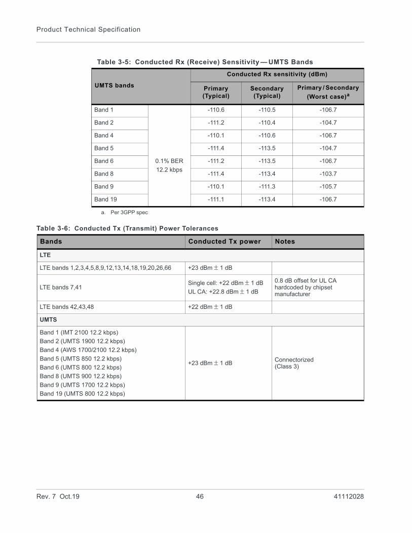
Product Technical Specification
Table 3-5: Conducted Rx (Receive) Sensitivity — UMTS Bands
UMTS bands
Conducted Rx sensitivity (dBm)
Primary(Typical)
Secondary(Typical)
Primary / Secondary
(Worst case)a
a. Per 3GPP specification
Band 1
0.1% BER
12.2 kbps
-110.6 -110.5 -106.7
Band 2 -111.2 -110.4 -104.7
Band 4 -110.1 -110.6 -106.7
Band 5 -111.4 -113.5 -104.7
Band 6 -111.2 -113.5 -106.7
Band 8 -111.4 -113.4 -103.7
Band 9 -110.1 -111.3 -105.7
Band 19 -111.1 -113.4 -106.7
Table 3-6: Conducted Tx (Transmit) Power Tolerances
Bands Conducted Tx power Notes
LTE
LTE bands 1,2,3,4,5,8,9,12,13,14,18,19,20,26,66 +23 dBm 1 dB
LTE bands 7,41Single cell: +22 dBm 1 dB
UL CA: +22.8 dBm 1 dB
0.8 dB offset for UL CA hardcoded by chipset manufacturer
LTE bands 42,43,48 +22 dBm 1 dB
UMTS
Band 1 (IMT 2100 12.2 kbps)
Band 2 (UMTS 1900 12.2 kbps)
Band 4 (AWS 1700/2100 12.2 kbps)
Band 5 (UMTS 850 12.2 kbps)
Band 6 (UMTS 800 12.2 kbps)
Band 8 (UMTS 900 12.2 kbps)
Band 9 (UMTS 1700 12.2 kbps)
Band 19 (UMTS 800 12.2 kbps)
+23 dBm 1 dB Connectorized(Class 3)
Rev. 7 Oct.19 46 41112028
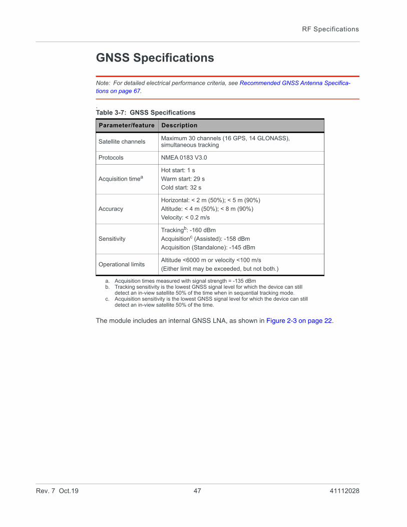
RF Specifications
GNSS Specifications
Note: For detailed electrical performance criteria, see Recommended GNSS Antenna Specifica-tions on page 67.
.
The module includes an internal GNSS LNA, as shown in Figure 2-3 on page 22.
Table 3-7: GNSS Specifications
Parameter/feature Description
Satellite channels Maximum 30 channels (16 GPS, 14 GLONASS), simultaneous tracking
Protocols NMEA 0183 V3.0
Acquisition timea
a. Acquisition times measured with signal strength = -135 dBm
Hot start: 1 s
Warm start: 29 s
Cold start: 32 s
Accuracy
Horizontal: < 2 m (50%); < 5 m (90%)
Altitude: < 4 m (50%); < 8 m (90%)
Velocity: < 0.2 m/s
Sensitivity
Trackingb: -160 dBm
Acquisitionc (Assisted): -158 dBm
Acquisition (Standalone): -145 dBm
b. Tracking sensitivity is the lowest GNSS signal level for which the device can still detect an in-view satellite 50% of the time when in sequential tracking mode.
c. Acquisition sensitivity is the lowest GNSS signal level for which the device can still detect an in-view satellite 50% of the time.
Operational limitsAltitude <6000 m or velocity <100 m/s
(Either limit may be exceeded, but not both.)
Rev. 7 Oct.19 47 41112028
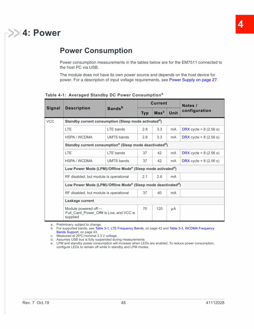
4
4: PowerPower Consumption
Power consumption measurements in the tables below are for the EM7511 connected to the host PC via USB.
The module does not have its own power source and depends on the host device for power. For a description of input voltage requirements, see Power Supply on page 27.
Table 4-1: Averaged Standby DC Power Consumptiona
Signal Description BandsbCurrent
Notes / configuration
Typ Maxc Unit
VCC Standby current consumption (Sleep mode activatedd)
LTE LTE bands 2.8 3.3 mA DRX cycle = 8 (2.56 s)
HSPA / WCDMA UMTS bands 2.8 3.3 mA DRX cycle = 8 (2.56 s)
Standby current consumptione (Sleep mode deactivatedd)
LTE LTE bands 37 42 mA DRX cycle = 8 (2.56 s)
HSPA / WCDMA UMTS bands 37 42 mA DRX cycle = 8 (2.56 s)
Low Power Mode (LPM)/Offline Modee (Sleep mode activatedd)
RF disabled, but module is operational 2.1 2.6 mA
Low Power Mode (LPM)/Offline Modee (Sleep mode deactivatedd)
RF disabled, but module is operational 37 40 mA
Leakage current
Module powered off—Full_Card_Power_Off# is Low, and VCC is supplied
70 120 A
a. Preliminary, subject to change.b. For supported bands, see Table 3-1, LTE Frequency Bands, on page 42 and Table 3-3, WCDMA Frequency
Bands Support, on page 43.c. Measured at 25ºC/nominal 3.3 V voltage.d. Assumes USB bus is fully suspended during measurementse. LPM and standby power consumption will increase when LEDs are enabled. To reduce power consumption,
configure LEDs to remain off while in standby and LPM modes.
Rev. 7 Oct.19 48 41112028
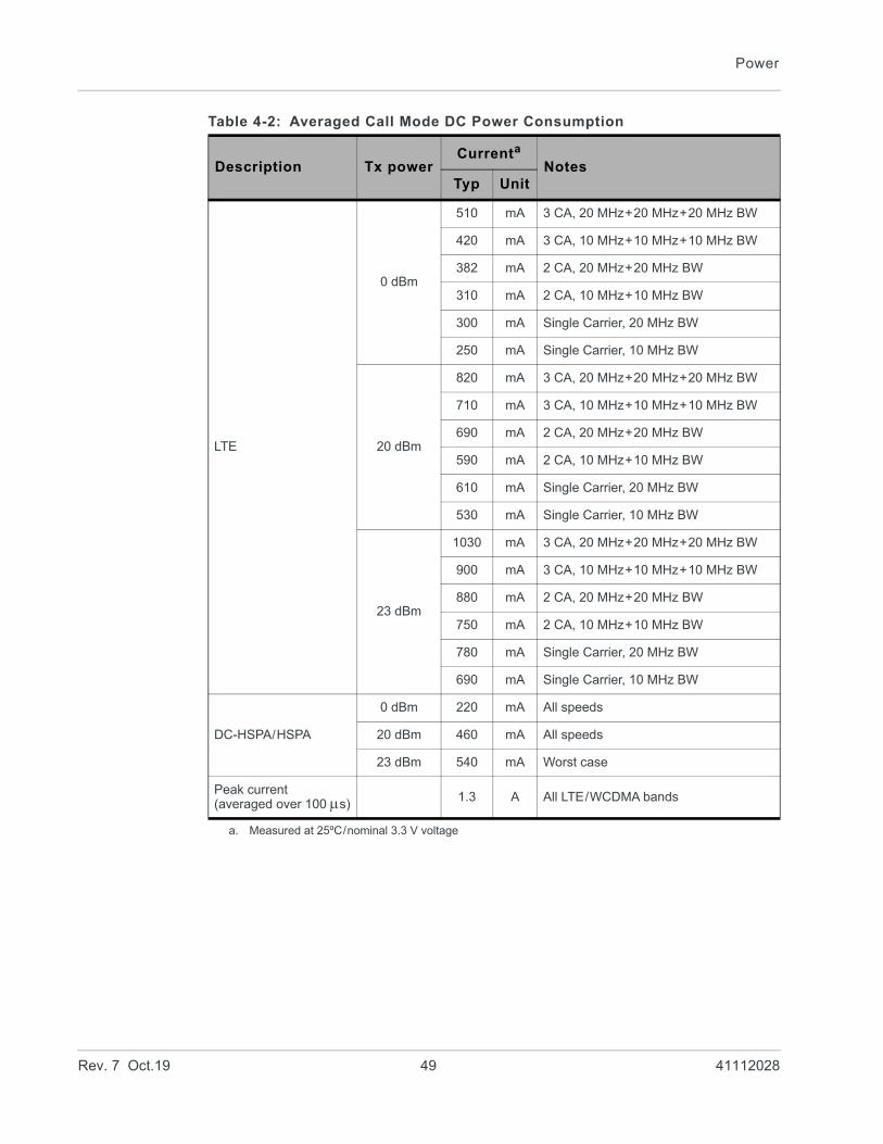
Power
Table 4-2: Averaged Call Mode DC Power Consumption
Description Tx powerCurrenta
NotesTyp Unit
LTE
0 dBm
510 mA 3 CA, 20 MHz+20 MHz+20 MHz BW
420 mA 3 CA, 10 MHz+10 MHz+10 MHz BW
382 mA 2 CA, 20 MHz+20 MHz BW
310 mA 2 CA, 10 MHz+10 MHz BW
300 mA Single Carrier, 20 MHz BW
250 mA Single Carrier, 10 MHz BW
20 dBm
820 mA 3 CA, 20 MHz+20 MHz+20 MHz BW
710 mA 3 CA, 10 MHz+10 MHz+10 MHz BW
690 mA 2 CA, 20 MHz+20 MHz BW
590 mA 2 CA, 10 MHz+10 MHz BW
610 mA Single Carrier, 20 MHz BW
530 mA Single Carrier, 10 MHz BW
23 dBm
1030 mA 3 CA, 20 MHz+20 MHz+20 MHz BW
900 mA 3 CA, 10 MHz+10 MHz+10 MHz BW
880 mA 2 CA, 20 MHz+20 MHz BW
750 mA 2 CA, 10 MHz+10 MHz BW
780 mA Single Carrier, 20 MHz BW
690 mA Single Carrier, 10 MHz BW
DC-HSPA/HSPA
0 dBm 220 mA All speeds
20 dBm 460 mA All speeds
23 dBm 540 mA Worst case
Peak current(averaged over 100 s) 1.3 A All LTE/WCDMA bands
a. Measured at 25ºC/nominal 3.3 V voltage
Rev. 7 Oct.19 49 41112028
Product Technical Specification
Warning: The maximum RF power level allowable on any RF port is +10dBm—damage may occur if this level is exceeded.
Module Power States
The module has five power states, as described in Table 4-4.
Table 4-3: Miscellaneous DC Power Consumption
Signal Description
Current / Voltage
Unit Notes / configurationMin Typ Max
VCC
USB active current — 15 20 mAHigh speed USB connection, CL = 50 pF on D+ and D- signals
Inrush current — 2.2 2.5 A
• Assumes power supply turn on time > 100µs
• Dependent on host power supply rise time.
Maximum current — — 1.5 A• Across all bands, all temperature
ranges
• 3.3 V supply
GNSS Signal connector Active bias on GNSS port
— — 100 mA Voltage applied to the GNSS antenna to power electronics inside the antenna (GNSS RF connector in Figure 3-1 on page 37).
3.05 3.15 3.25 V
Table 4-4: Module Power States
State Details
Ho
st
is p
ow
ere
d
US
B i
nte
rfa
ce
ac
tiv
e
RF
en
ab
led
Normal(Default state)
• Module is active
• Default state. Occurs when VCC is first applied, Full_Card_Power_Off# is deasserted (pulled high), and W_DISABLE# is deasserted
• Module is capable of placing/receiving calls, or establishing data connections on the wireless network
• Current consumption is affected by several factors, including:
• Radio band being used
• Transmit power
• Receive gain settings
• Data rate
Rev. 7 Oct.19 50 41112028
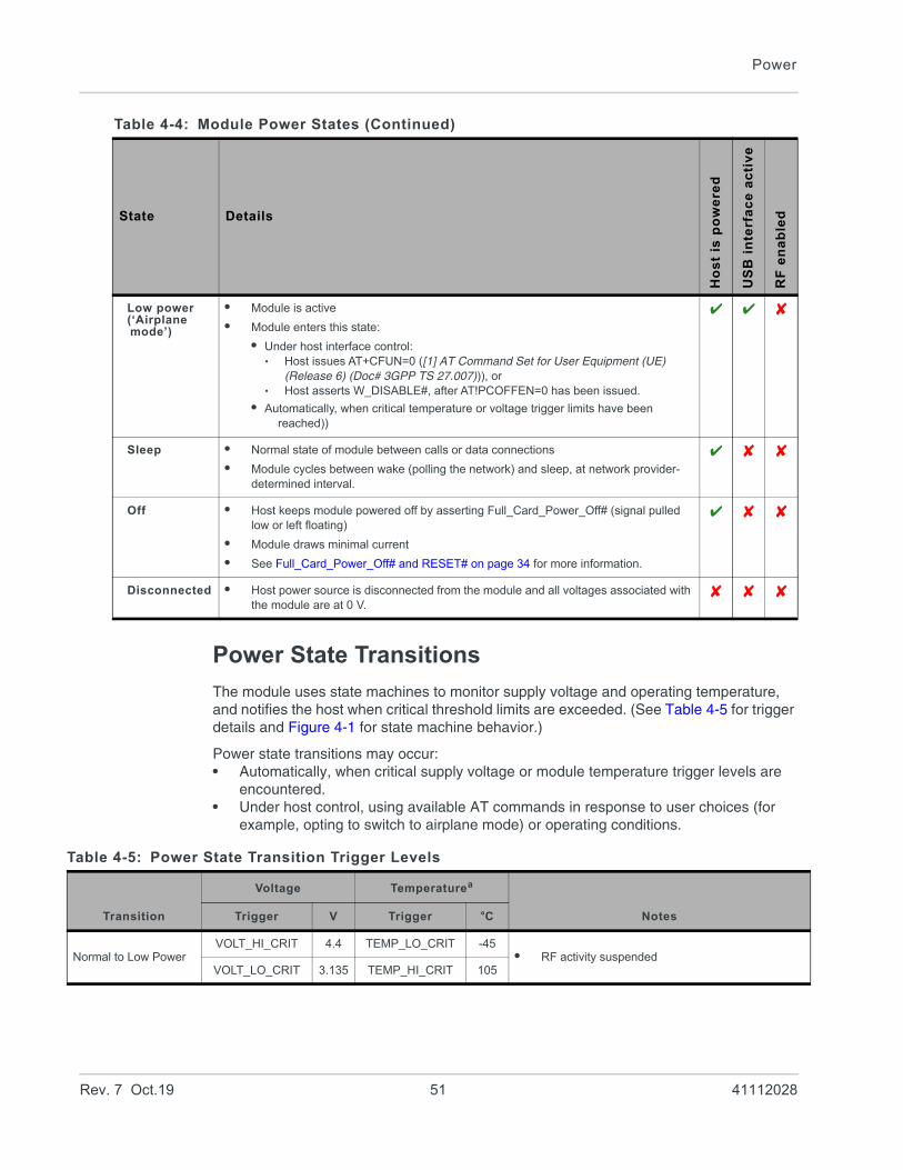
Power
Power State Transitions
The module uses state machines to monitor supply voltage and operating temperature, and notifies the host when critical threshold limits are exceeded. (See Table 4-5 for trigger details and Figure 4-1 for state machine behavior.)
Power state transitions may occur:• Automatically, when critical supply voltage or module temperature trigger levels are
encountered.• Under host control, using available AT commands in response to user choices (for
example, opting to switch to airplane mode) or operating conditions.
Low power(‘Airplane mode’)
• Module is active
• Module enters this state:
• Under host interface control:· Host issues AT+CFUN=0 ([1] AT Command Set for User Equipment (UE)
(Release 6) (Doc# 3GPP TS 27.007))), or· Host asserts W_DISABLE#, after AT!PCOFFEN=0 has been issued.
• Automatically, when critical temperature or voltage trigger limits have been reached))
Sleep • Normal state of module between calls or data connections
• Module cycles between wake (polling the network) and sleep, at network provider-determined interval.
Off • Host keeps module powered off by asserting Full_Card_Power_Off# (signal pulled low or left floating)
• Module draws minimal current
• See Full_Card_Power_Off# and RESET# on page 34 for more information.
Disconnected • Host power source is disconnected from the module and all voltages associated with the module are at 0 V.
Table 4-4: Module Power States (Continued)
State Details
Ho
st
is p
ow
ere
d
US
B i
nte
rfa
ce
ac
tiv
e
RF
en
ab
led
Table 4-5: Power State Transition Trigger Levels
Transition
Voltage Temperaturea
Notes Trigger V Trigger °C
Normal to Low PowerVOLT_HI_CRIT 4.4 TEMP_LO_CRIT -45
• RF activity suspendedVOLT_LO_CRIT 3.135 TEMP_HI_CRIT 105
Rev. 7 Oct.19 51 41112028
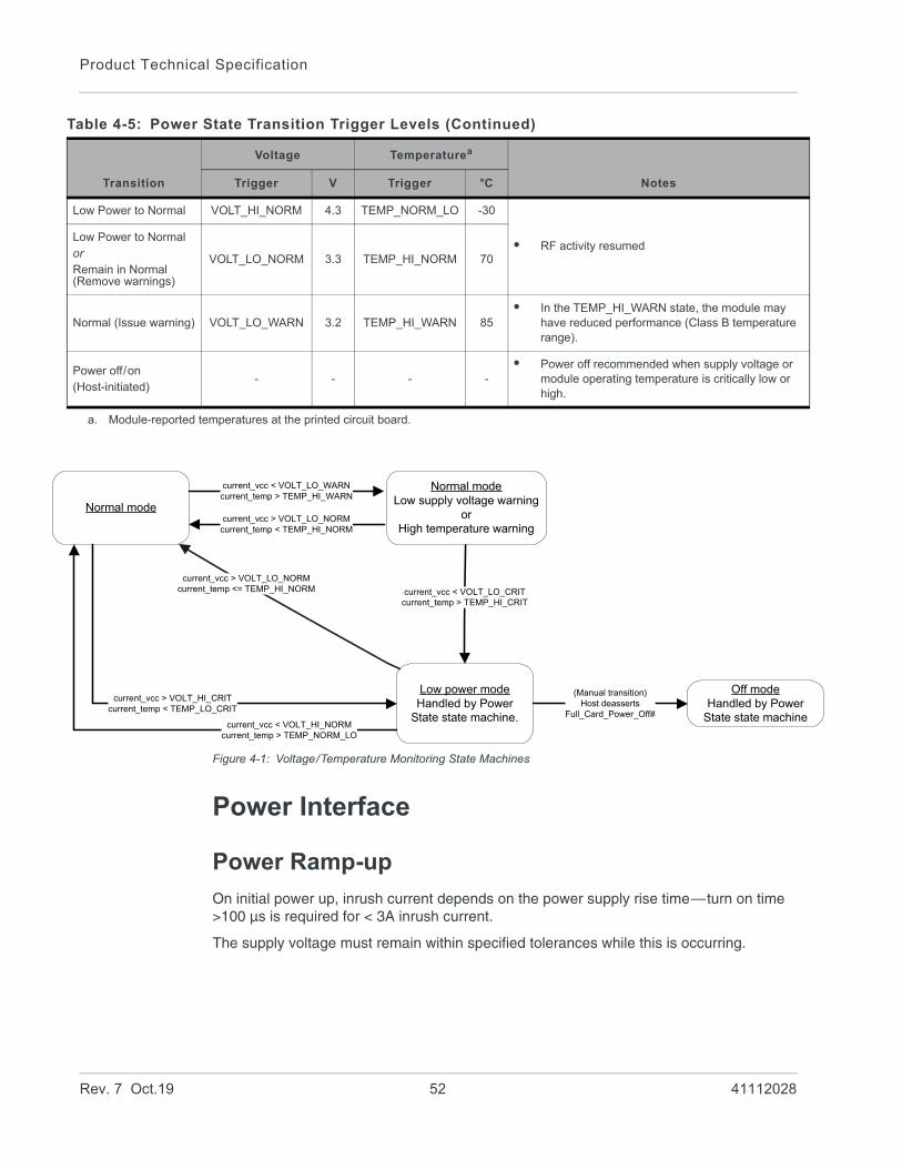
Product Technical Specification
Figure 4-1: Voltage/Temperature Monitoring State Machines
Power Interface
Power Ramp-up
On initial power up, inrush current depends on the power supply rise time—turn on time >100 µs is required for < 3A inrush current.
The supply voltage must remain within specified tolerances while this is occurring.
Low Power to Normal VOLT_HI_NORM 4.3 TEMP_NORM_LO -30
• RF activity resumedLow Power to NormalorRemain in Normal (Remove warnings)
VOLT_LO_NORM 3.3 TEMP_HI_NORM 70
Normal (Issue warning) VOLT_LO_WARN 3.2 TEMP_HI_WARN 85• In the TEMP_HI_WARN state, the module may
have reduced performance (Class B temperature range).
Power off/on(Host-initiated)
- - - -• Power off recommended when supply voltage or
module operating temperature is critically low or high.
a. Module-reported temperatures at the printed circuit board.
Table 4-5: Power State Transition Trigger Levels (Continued)
Transition
Voltage Temperaturea
Notes Trigger V Trigger °C
Off modeHandled by Power
State state machine
Normal mode
Low power modeHandled by Power
State state machine.
current_vcc > VOLT_LO_NORMcurrent_temp <= TEMP_HI_NORM current_vcc < VOLT_LO_CRIT
current_temp > TEMP_HI_CRIT
current_vcc > VOLT_LO_NORMcurrent_temp < TEMP_HI_NORM
current_vcc < VOLT_LO_WARNcurrent_temp > TEMP_HI_WARN
current_vcc < VOLT_HI_NORMcurrent_temp > TEMP_NORM_LO
current_vcc > VOLT_HI_CRITcurrent_temp < TEMP_LO_CRIT
(Manual transition)Host deasserts
Full_Card_Power_Off#
Normal modeLow supply voltage warning
orHigh temperature warning
Rev. 7 Oct.19 52 41112028
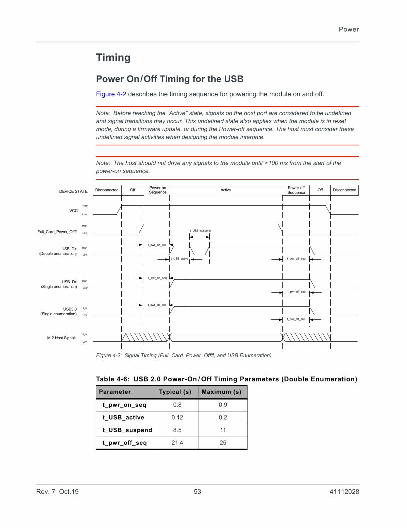
Power
Timing
Power On/Off Timing for the USB
Figure 4-2 describes the timing sequence for powering the module on and off.
Note: Before reaching the “Active” state, signals on the host port are considered to be undefined and signal transitions may occur. This undefined state also applies when the module is in reset mode, during a firmware update, or during the Power-off sequence. The host must consider these undefined signal activities when designing the module interface.
Note: The host should not drive any signals to the module until >100 ms from the start of the power-on sequence.
Figure 4-2: Signal Timing (Full_Card_Power_Off#, and USB Enumeration)
Full_Card_Power_Off#
Disconnected Power-on Sequence
USB_D+(Double enumeration)
Power-off Sequence
DisconnectedActiveDEVICE STATE
High
Low
High
Low
Off Off
High
VCCLow
t_pwr_on_seq
t_USB_active
t_USB_suspend
t_pwr_off_seq
USB_D+(Single enumeration)
High
Low
t_pwr_on_seq
t_pwr_off_seq
USB3.0(Single enumeration)
High
Low
t_pwr_on_seq
t_pwr_off_seq
M.2 Host SignalsHigh
Low
Table 4-6: USB 2.0 Power-On / Off Timing Parameters (Double Enumeration)
Parameter Typical (s) Maximum (s)
t_pwr_on_seq 0.8 0.9
t_USB_active 0.12 0.2
t_USB_suspend 8.5 11
t_pwr_off_seq 21.4 25
Rev. 7 Oct.19 53 41112028
Product Technical Specification
USB Enumeration
The unit supports single and double USB enumeration with the host:• Single enumeration:
· Enumeration starts within maximum t_pwr_on_seq seconds of power-on.• Double enumeration—As shown in Figure 4-2:
· First enumeration starts within t_pwr_on_seq seconds of power-on (while USB_D+ is high)
· Second enumeration starts after t_USB_suspend (when USB_D+ goes high again)
Reset Timing
To reset the module, refer to Table 2-7 on page 35 for RESET# signal usage instructions.
Required Shutdown Sequence
Warning: To avoid causing issues with the file system, follow this shutdown sequence.
1. Drive Full_Card_Power_Off# low.
2. Wait for at least t_pwr_off_seq seconds.
3. Remove power.
Power Supply Noise
Noise in the power supply can lead to noise in the RF signal.
The power supply ripple limit for the module is no more than 100 mVp-p 1 Hz to 100 kHz. This limit includes voltage ripple due to transmitter burst activity.
Additional decoupling capacitors can be added to the main VCC line to filter noise into the device.
Table 4-7: USB 2.0 Power-On / Off Timing Parameters (Single Enumeration)
Parameter Typical (s) Maximum (s)
t_pwr_on_seq 8.7 11
t_pwr_off_seq 21.4 25
Table 4-8: USB 3.0 Power-On / Off Timing Parameters (Single Enumeration)
Parameter Typical (s) Maximum (s)
t_pwr_on_seq 8.6 11
t_pwr_off_seq 21.5 25
Rev. 7 Oct.19 54 41112028
Power
SED (Smart Error Detection)
The module uses a form of SED to track premature modem resets.• Module tracks consecutive resets occuring soon after power-on.• After a sixth consecutive reset, the module waits in boot-and-hold mode for a
firmware download to resolve the power-cycle problem.
Tx Power Control
The module’s Tx power limit may be controlled using either SAR backoff AT commands, defined in [2] AirPrime EM75xx AT Command Reference (Doc# 41111748), or the DPR (Dynamic power control) signal. Use the GPIOSARENABLE parameter for !CUSTOM to choose the method:• AT commands:
· !SARSTATEDFLT—Set (or report) the default SAR backoff state that the device uses when it powers up. This setting is persistent across power cycles and overrides any PRI setting.
· !SARSTATE—Set (or report) the current SAR backoff state (override the default state). This change in state is non-persistent across power cycles.
· !SARBACKOFF—Set (or report) the maximum Tx power limit for a specific band/technology/state combination.
Note: A customization is available to invert the DPR logic. (e.g. make DPR low = No SAR backoff)
• Dynamic power control— The module’s firmware monitors DPR (pin 25) and adjusts the RF Tx power appropriately, as detailed in Table 4-9. (This state change is equiv-alent to issuing the !SARSTATE AT command.)
Note: The host can implement an open collector drive for the DPR pin (if a 1.8 V-compatible drive is not available).
Table 4-9: Dynamic Power Control of SAR Backoff State
DPR SAR backoff state
Higha
a. DPR is pulled high by default.
No SAR backof
Low Backoff 1
Rev. 7 Oct.19 55 41112028
Rev. 7 Oct.19 56 41112028
55: Software Interface
Support Tools
The EM7511 is compatible with the following support tools from Sierra Wireless and authorized third parties:• Firmware update utilities from Sierra Wireless• Sierra Wireless Logger• QXDM from QUALCOMM• QUALCOMM Product Support Tool (QPST)• Windows and Linux SDKs (including API and drivers)
Host Interface
The device supports the following protocols for modem communication:• MBIM (Mobile Broadband Interface Model)• Qualcomm QMI interface. (Please contact your Sierra Wireless account represen-
tative for QMI interface documentation.)
6
6: Mechanical and Environmental Specifica-tionsThe EM7511 module complies with the mechanical and environmental specifications in Table 6-1. Final product conformance to these specifications depends on the OEM device implementation.
Table 6-1: Mechanical and Environmental Specifications
Mode Details
Ambient temperature Operational Class A
-30ºC to +70ºC – 3GPP compliant
Operational Class B
-40ºC to +85ºC, with appropriate heatsinking – non-3GPP compliant (reduced operating parameters required)
Non-operational -40ºC to +85ºC, 96 hours
(from MIL-STD 202 Method 108)
Relative humidity Non-operational 85ºC, 85% relative humidity for 48 hours (non-condensing)
Vibration Non-operational Random vibration, 10 to 2000 Hz, 0.1 g2/Hz to0.0005 g2/Hz, in each of three mutually perpendicular axes. Test duration of 60 minutes for each axis, for a total test time of three hours.
Shock Non-operational Half sine shock, 11 ms, 30 g, 8x each axisHalf sine shock, 6 ms, 100 g, 3x each axis
Drop Non-operational 1 m on concrete on each of six faces, two times (module only)
(Electrostatic discharge (See Electrostatic Discharge (ESD) on page 59.)
Operational The RF port (antenna launch and RF connector) complies with the IEC 61000-4-2 standard:
• Electrostatic Discharge Immunity: Test: Level3Air Discharge: ±8 kV
Non-operational The host connector interface complies with the following standard only:
• minimum ±500 V Human Body Model (JESD22-A114-B)
Thermal considerations See Thermal Considerations on page 60.
Form factor M.2 Form Factor
Dimensions Length: 42±0.15 mm (max)
Width: 30±0.15 mm (max)
Thickness: Above PCB—1.50 mm (max)PCB—0.88 mm (max)
Weight: 6.5 g
Rev. 7 Oct.19 57 41112028
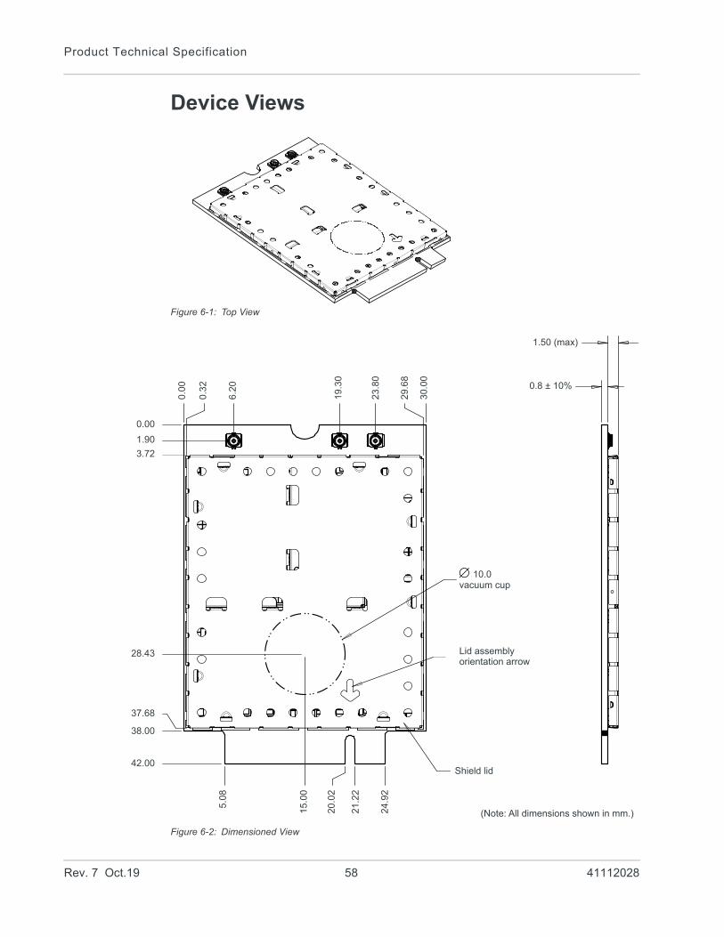
Product Technical Specification
Device Views
Figure 6-1: Top View
Figure 6-2: Dimensioned View
1.50 (max)
0.00
10.0
1.90
(Note: All dimensions shown in mm.)
0.8 ± 10%
3.72
28.43
37.68
38.00
42.00
5.08
15.0
0
20.0
2
21.2
2
24.9
2
0.00
0.32
6.20
19.3
0
23.8
0
29.6
8
30.0
0
vacuum cup
Lid assemblyorientation arrow
Shield lid
Rev. 7 Oct.19 58 41112028
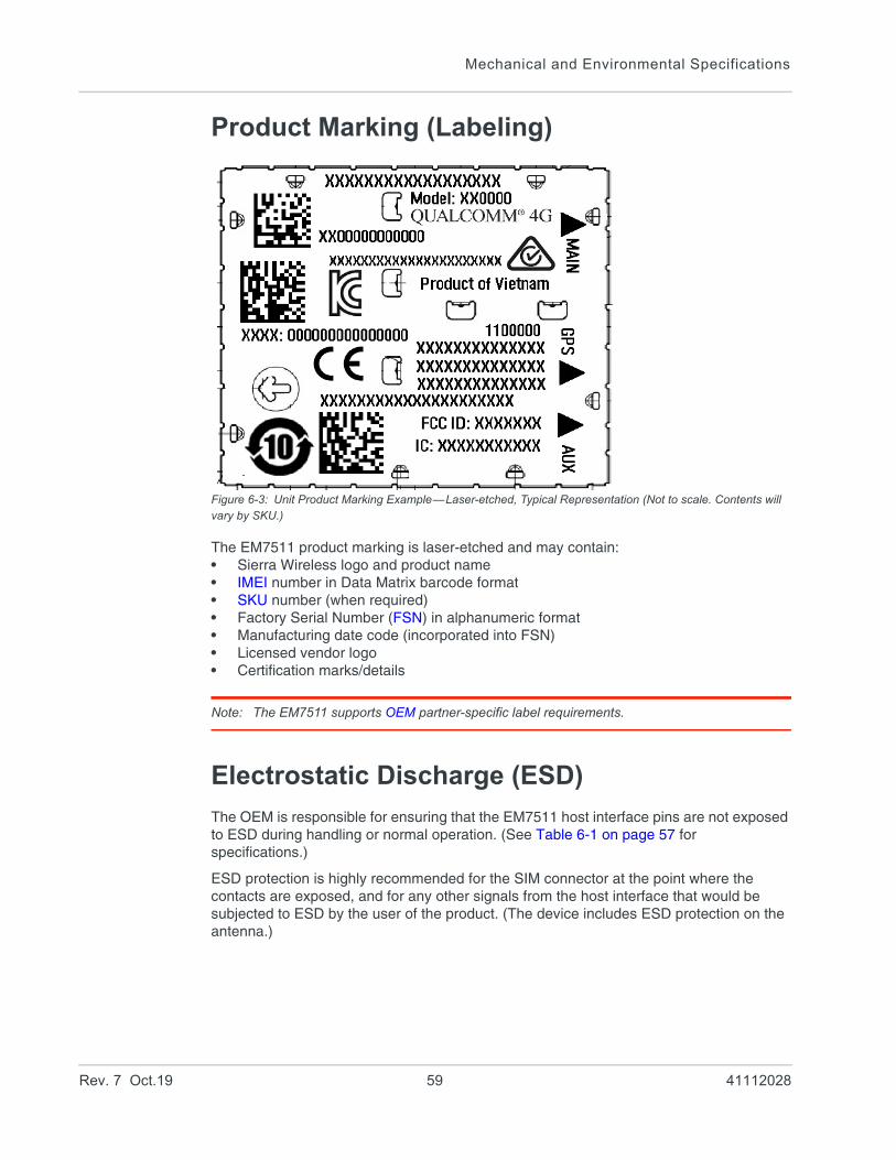
Mechanical and Environmental Specifications
Product Marking (Labeling)
Figure 6-3: Unit Product Marking Example—Laser-etched, Typical Representation (Not to scale. Contents will vary by SKU.)
The EM7511 product marking is laser-etched and may contain:• Sierra Wireless logo and product name• IMEI number in Data Matrix barcode format• SKU number (when required)• Factory Serial Number (FSN) in alphanumeric format• Manufacturing date code (incorporated into FSN)• Licensed vendor logo• Certification marks/details
Note: The EM7511 supports OEM partner-specific label requirements.
Electrostatic Discharge (ESD)
The OEM is responsible for ensuring that the EM7511 host interface pins are not exposed to ESD during handling or normal operation. (See Table 6-1 on page 57 for specifications.)
ESD protection is highly recommended for the SIM connector at the point where the contacts are exposed, and for any other signals from the host interface that would be subjected to ESD by the user of the product. (The device includes ESD protection on the antenna.)
Rev. 7 Oct.19 59 41112028
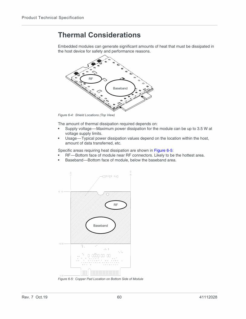
Product Technical Specification
Thermal Considerations
Embedded modules can generate significant amounts of heat that must be dissipated in the host device for safety and performance reasons.
Figure 6-4: Shield Locations (Top View)
The amount of thermal dissipation required depends on:• Supply voltage—Maximum power dissipation for the module can be up to 3.5 W at
voltage supply limits.• Usage—Typical power dissipation values depend on the location within the host,
amount of data transferred, etc.
Specific areas requiring heat dissipation are shown in Figure 6-5:• RF—Bottom face of module near RF connectors. Likely to be the hottest area.• Baseband—Bottom face of module, below the baseband area.
Figure 6-5: Copper Pad Location on Bottom Side of Module
RF
Baseband
Baseband
RF
Rev. 7 Oct.19 60 41112028
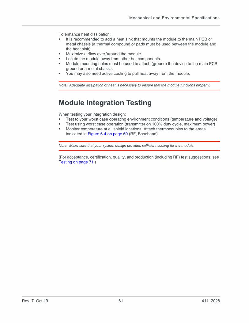
Mechanical and Environmental Specifications
To enhance heat dissipation:• It is recommended to add a heat sink that mounts the module to the main PCB or
metal chassis (a thermal compound or pads must be used between the module and the heat sink).
• Maximize airflow over/around the module.• Locate the module away from other hot components.• Module mounting holes must be used to attach (ground) the device to the main PCB
ground or a metal chassis.• You may also need active cooling to pull heat away from the module.
Note: Adequate dissipation of heat is necessary to ensure that the module functions properly.
Module Integration Testing
When testing your integration design:• Test to your worst case operating environment conditions (temperature and voltage)• Test using worst case operation (transmitter on 100% duty cycle, maximum power)• Monitor temperature at all shield locations. Attach thermocouples to the areas
indicated in Figure 6-4 on page 60 (RF, Baseband).
Note: Make sure that your system design provides sufficient cooling for the module.
(For acceptance, certification, quality, and production (including RF) test suggestions, see Testing on page 71.)
Rev. 7 Oct.19 61 41112028
7
7: Regulatory Compliance and Industry Certifi-cationsThe EM7511 module is designed to meet, and upon commercial release, will meet the requirements of the following regulatory bodies and regulations, where applicable:• Federal Communications Commission (FCC) of the United States• The Certification and Engineering Bureau of Industry Canada (IC)• The National Communications Commission (NCC) of Taiwan, Republic of China
The EM7511 Embedded Module complies with the mandatory requirements described in the following standards. The exact set of requirements supported is network operator-dependent.
Upon commercial release, the following industry certifications will have been obtained, where applicable:• GCF• PTCRB
Additional certifications and details on specific country approvals may be obtained upon customer request—contact your Sierra Wireless account representative for details.
Additional testing and certification may be required for the end product with an embedded EM7511 module and are the responsibility of the OEM. Sierra Wireless offers professional services-based assistance to OEMs with the testing and certification process, if required.
Important Compliance Information for the United States and Canada
The EM7511 module, upon commercial release, will have been granted modular approval for mobile applications. Integrators may use the EM7511 module in their final products without additional FCC/IC (Industry Canada) certification if they meet the following conditions. Otherwise, additional FCC/IC approvals must be obtained.
1. At least 20 cm separation distance between the antenna and the user’s body must be maintained at all times.
2. To comply with FCC/IC regulations limiting both maximum RF output power and human exposure to RF radiation, the maximum antenna gain including cable loss in a mobile-only exposure condition must not exceed the limits stipulated in Table 7-2 on page 63.
Table 7-1: Standards Compliance
Technology Standards
LTE • 3GPP Release 11a
a. Some auxiliary functions support Release 12 or Release 13.
UMTS • 3GPP Release 9
Rev. 7 Oct.19 62 41112028
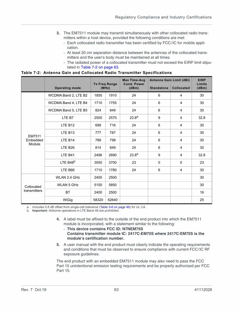
Regulatory Compliance and Industry Certifications
3. The EM7511 module may transmit simultaneously with other collocated radio trans-mitters within a host device, provided the following conditions are met:· Each collocated radio transmitter has been certified by FCC/IC for mobile appli-
cation.· At least 20 cm separation distance between the antennas of the collocated trans-
mitters and the user’s body must be maintained at all times.· The radiated power of a collocated transmitter must not exceed the EIRP limit stipu-
lated in Table 7-2 on page 63.
4. A label must be affixed to the outside of the end product into which the EM7511 module is incorporated, with a statement similar to the following:· This device contains FCC ID: N7NEM75S
Contains transmitter module IC: 2417C-EM75S where 2417C-EM75S is the module’s certification number.
5. A user manual with the end product must clearly indicate the operating requirements and conditions that must be observed to ensure compliance with current FCC/IC RF exposure guidelines.
The end product with an embedded EM7511 module may also need to pass the FCC Part 15 unintentional emission testing requirements and be properly authorized per FCC Part 15.
Table 7-2: Antenna Gain and Collocated Radio Transmitter Specifications
Operating modeTx Freq Range
(MHz)
Max Time-Avg Cond. Power
(dBm)
Antenna Gain Limit (dBi) EIRP Limits (dBm)Standalone Collocated
EM7511 Embedded
Module
WCDMA Band 2, LTE B2 1850 1910 24 6 4 30
WCDMA Band 4, LTE B4 1710 1755 24 6 4 30
WCDMA Band 5, LTE B5 824 849 24 6 4 30
LTE B7 2500 2570 23.8a 9 4 32.8
LTE B12 699 716 24 6 4 30
LTE B13 777 787 24 6 4 30
LTE B14 788 798 24 6 4 30
LTE B26 814 849 24 6 4 30
LTE B41 2496 2690 23.8a 9 4 32.8
LTE B48b 3550 3700 23 0 0 23
LTE B66 1710 1780 24 6 4 30
Collocatedtransmitters
WLAN 2.4 GHz 2400 2500 30
WLAN 5 GHz 5150 5850 30
BT 2400 2500 16
WiGig 58320 62640 25
a. Includes 0.8 dB offset from single-cell tolerance (Table 3-6 on page 46) for UL CA.b. Important: Airborne operations in LTE Band 48 are prohibited.
Rev. 7 Oct.19 63 41112028
Product Technical Specification
Note: If this module is intended for use in a portable device, you are responsible for separate approval to satisfy the SAR requirements of FCC Part 2.1093 and IC RSS-102.
Rev. 7 Oct.19 64 41112028
A
A: Antenna SpecificationThis appendix describes recommended electrical performance criteria for main path, diversity path, and GNSS antennas used with AirPrime embedded modules.
The performance specifications described in this section are valid while antennas are mounted in the host device with antenna feed cables routed in their final application configuration.
Note: Antennas should be designed before the industrial design is finished to make sure that the best antennas can be developed
Recommended Main/Diversity Antenna Specifications
Table A-1: Antenna Requirements a
Parameter Requirements Comments
Antenna system (LTE) External multi-band 2x2 MIMO antenna system (Ant1/Ant2)b
(3G) External multi-band antenna system with diversity (Ant1/Ant2)c
If Ant2 includes GNSS, then it must also satisfy requirements in Table A-2 on page 67.
Operating bands —Antenna 1
All supporting Tx and Rx frequency bands.
Operating bands —Antenna 2
All supporting Rx frequency bands, plus GNSS frequency bands if Antenna 2 is used in shared Diversity/MIMO/GNSS mode.
VSWR of Ant1 and Ant2 • < 2:1 (recommended)
• < 3:1 (worst case)
On all bands including band edges
Total radiated efficiency of Ant1 and Ant2
> 50% on all bands • Measured at the RF connector.
• Includes mismatch losses, losses in the matching circuit, and antenna losses, excluding cable loss.
• Sierra Wireless recommends using antenna efficiency as the primary parameter for evaluating the antenna system.Peak gain is not a good indication of antenna performance when integrated with a host device (the antenna does not provide omni-directional gain patterns). Peak gain can be affected by antenna size, location, design type, etc.—the antenna gain patterns remain fixed unless one or more of these parameters change.
Rev. 7 Oct.19 65 41112028
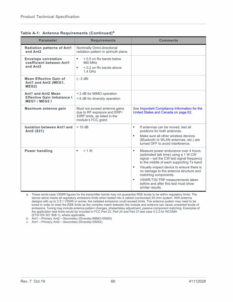
Product Technical Specification
Radiation patterns of Ant1 and Ant2
Nominally Omni-directional radiation pattern in azimuth plane.
Envelope correlation coefficient between Ant1 and Ant2
• < 0.5 on Rx bands below 960 MHz
• < 0.2 on Rx bands above 1.4 GHz
Mean Effective Gain of Ant1 and Ant2 (MEG1, MEG2)
-3 dBi
Ant1 and Ant2 Mean Effective Gain Imbalance I MEG1 / MEG2 I
< 2 dB for MIMO operation
< 6 dB for diversity operation
Maximum antenna gain Must not exceed antenna gains due to RF exposure and ERP/EIRP limits, as listed in the module’s FCC grant.
See Important Compliance Information for the United States and Canada on page 62.
Isolation between Ant1 and Ant2 (S21)
> 10 dB • If antennas can be moved, test all positions for both antennas.
• Make sure all other wireless devices (Bluetooth or WLAN antennas, etc.) are turned OFF to avoid interference.
Power handling • > 1 W • Measure power endurance over 4 hours (estimated talk time) using a 1 W CW signal—set the CW test signal frequency to the middle of each supporting Tx band.
• Visually inspect device to ensure there is no damage to the antenna structure and matching components.
• VSWR/TIS/TRP measurements taken before and after this test must show similar results.
a. These worst-case VSWR figures for the transmitter bands may not guarantee RSE levels to be within regulatory limits. The device alone meets all regulatory emissions limits when tested into a cabled (conducted) 50 ohm system. With antenna designs with up to 2.5:1 VSWR or worse, the radiated emissions could exceed limits. The antenna system may need to be tuned in order to meet the RSE limits as the complex match between the module and antenna can cause unwanted levels of emissions. Tuning may include antenna pattern changes, phase/delay adjustment, passive component matching. Examples of the application test limits would be included in FCC Part 22, Part 24 and Part 27,test case 4.2.2 for WCDMA (ETSI EN 301 908-1), where applicable.
b. Ant1—Primary, Ant2—Secondary (Diversity/MIMO/GNSS)c. Ant1—Primary, Ant2—Secondary (Diversity/GNSS)
Table A-1: Antenna Requirements (Continued)a
Parameter Requirements Comments
Rev. 7 Oct.19 66 41112028
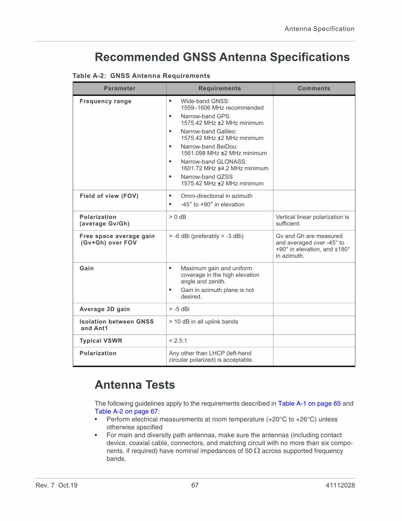
Antenna Specification
Recommended GNSS Antenna Specifications
Antenna Tests
The following guidelines apply to the requirements described in Table A-1 on page 65 and Table A-2 on page 67:• Perform electrical measurements at room temperature (+20°C to +26°C) unless
otherwise specified• For main and diversity path antennas, make sure the antennas (including contact
device, coaxial cable, connectors, and matching circuit with no more than six compo-nents, if required) have nominal impedances of 50 across supported frequency bands.
Table A-2: GNSS Antenna Requirements
Parameter Requirements Comments
Frequency range • Wide-band GNSS:1559–1606 MHz recommended
• Narrow-band GPS:1575.42 MHz ±2 MHz minimum
• Narrow-band Galileo:1575.42 MHz ±2 MHz minimum
• Narrow-band BeiDou:1561.098 MHz ±2 MHz minimum
• Narrow-band GLONASS:1601.72 MHz ±4.2 MHz minimum
• Narrow-band QZSS1575.42 MHz ±2 MHz minimum
Field of view (FOV) • Omni-directional in azimuth
• -45° to +90° in elevation
Polarization(average Gv/Gh)
> 0 dB Vertical linear polarization is sufficient.
Free space average gain (Gv+Gh) over FOV
> -6 dBi (preferably > -3 dBi) Gv and Gh are measured and averaged over -45° to +90° in elevation, and ±180° in azimuth.
Gain • Maximum gain and uniform coverage in the high elevation angle and zenith.
• Gain in azimuth plane is not desired.
Average 3D gain > -5 dBi
Isolation between GNSS and Ant1
> 10 dB in all uplink bands
Typical VSWR < 2.5:1
Polarization Any other than LHCP (left-hand circular polarized) is acceptable.
Rev. 7 Oct.19 67 41112028
Product Technical Specification
• All tests (except isolation/correlation coefficient)—Test the main or diversity antenna with the other antenna terminated.
• Any metallic part of the antenna system that is exposed to the outside environment needs to meet the electrostatic discharge tests per IEC61000-4-2 (conducted discharge +8kV).
• The functional requirements of the antenna system are tested and verified while the embedded module’s antenna is integrated in the host device.
Note: Additional testing, including active performance tests, mechanical, and accelerated life tests can be discussed with Sierra Wireless’ engineering services. Contact your Sierra Wireless repre-sentative for assistance.
Rev. 7 Oct.19 68 41112028
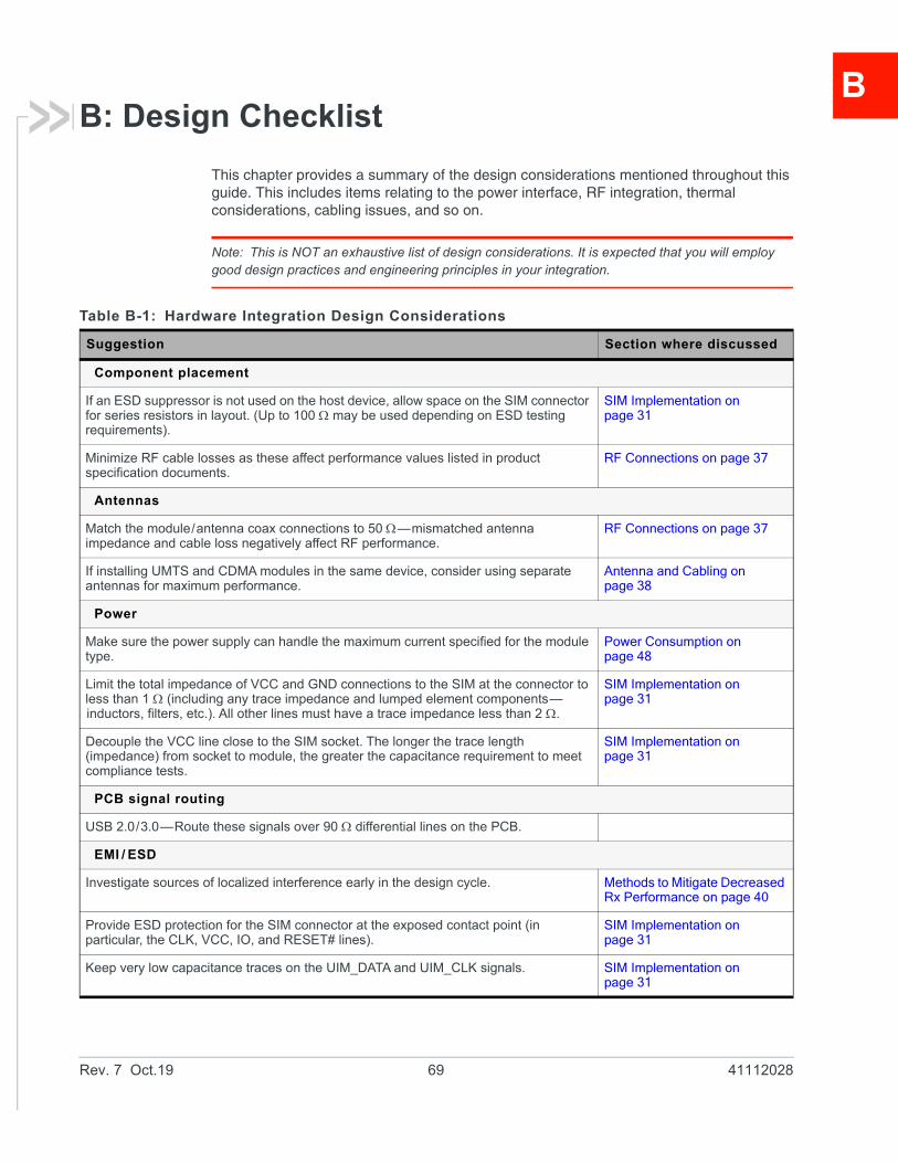
B
B: Design ChecklistThis chapter provides a summary of the design considerations mentioned throughout this guide. This includes items relating to the power interface, RF integration, thermal considerations, cabling issues, and so on.
Note: This is NOT an exhaustive list of design considerations. It is expected that you will employ good design practices and engineering principles in your integration.
Table B-1: Hardware Integration Design Considerations
Suggestion Section where discussed
Component placement
If an ESD suppressor is not used on the host device, allow space on the SIM connector for series resistors in layout. (Up to 100 may be used depending on ESD testing requirements).
SIM Implementation on page 31
Minimize RF cable losses as these affect performance values listed in product specification documents.
RF Connections on page 37
Antennas
Match the module/antenna coax connections to 50 —mismatched antenna impedance and cable loss negatively affect RF performance.
RF Connections on page 37
If installing UMTS and CDMA modules in the same device, consider using separate antennas for maximum performance.
Antenna and Cabling on page 38
Power
Make sure the power supply can handle the maximum current specified for the module type.
Power Consumption on page 48
Limit the total impedance of VCC and GND connections to the SIM at the connector to less than 1 (including any trace impedance and lumped element components—inductors, filters, etc.). All other lines must have a trace impedance less than 2 .
SIM Implementation on page 31
Decouple the VCC line close to the SIM socket. The longer the trace length (impedance) from socket to module, the greater the capacitance requirement to meet compliance tests.
SIM Implementation on page 31
PCB signal routing
USB 2.0/3.0—Route these signals over 90 differential lines on the PCB.
EMI / ESD
Investigate sources of localized interference early in the design cycle. Methods to Mitigate Decreased Rx Performance on page 40
Provide ESD protection for the SIM connector at the exposed contact point (in particular, the CLK, VCC, IO, and RESET# lines).
SIM Implementation on page 31
Keep very low capacitance traces on the UIM_DATA and UIM_CLK signals. SIM Implementation on page 31
Rev. 7 Oct.19 69 41112028
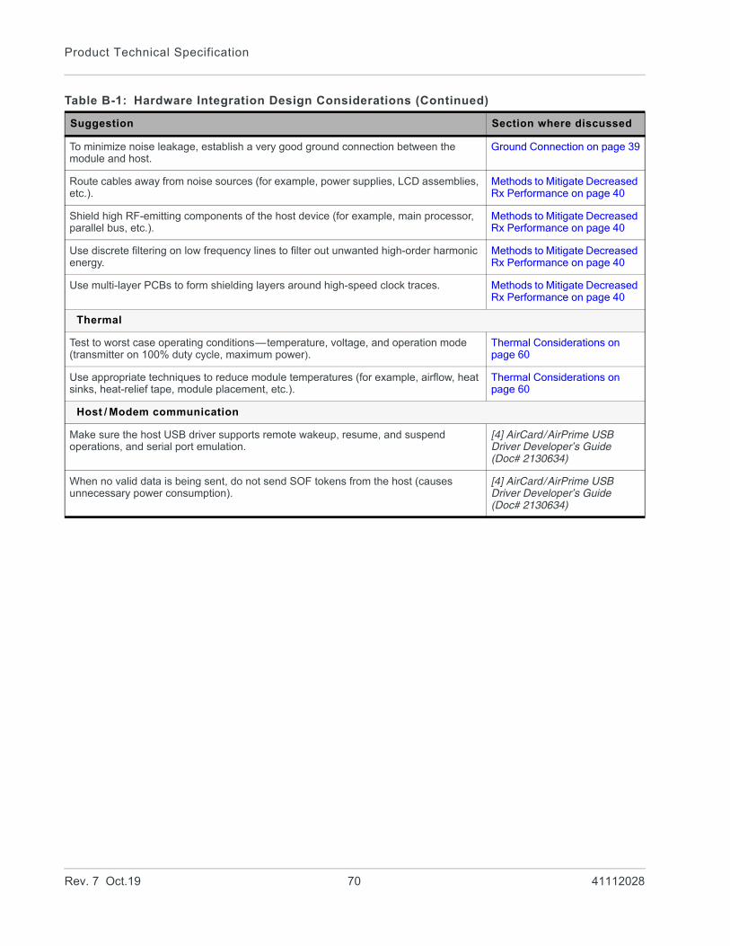
Product Technical Specification
To minimize noise leakage, establish a very good ground connection between the module and host.
Ground Connection on page 39
Route cables away from noise sources (for example, power supplies, LCD assemblies, etc.).
Methods to Mitigate Decreased Rx Performance on page 40
Shield high RF-emitting components of the host device (for example, main processor, parallel bus, etc.).
Methods to Mitigate Decreased Rx Performance on page 40
Use discrete filtering on low frequency lines to filter out unwanted high-order harmonic energy.
Methods to Mitigate Decreased Rx Performance on page 40
Use multi-layer PCBs to form shielding layers around high-speed clock traces. Methods to Mitigate Decreased Rx Performance on page 40
Thermal
Test to worst case operating conditions—temperature, voltage, and operation mode (transmitter on 100% duty cycle, maximum power).
Thermal Considerations on page 60
Use appropriate techniques to reduce module temperatures (for example, airflow, heat sinks, heat-relief tape, module placement, etc.).
Thermal Considerations on page 60
Host / Modem communication
Make sure the host USB driver supports remote wakeup, resume, and suspend operations, and serial port emulation.
[4] AirCard/AirPrime USB Driver Developer’s Guide (Doc# 2130634)
When no valid data is being sent, do not send SOF tokens from the host (causes unnecessary power consumption).
[4] AirCard/AirPrime USB Driver Developer’s Guide (Doc# 2130634)
Table B-1: Hardware Integration Design Considerations (Continued)
Suggestion Section where discussed
Rev. 7 Oct.19 70 41112028
C
C: TestingNote: All AirPrime embedded modules are factory-tested to ensure they conform to published product specifications.
Developers of OEM devices integrating Sierra Wireless AirPrime embedded modules should include a series of test phases in their manufacturing process to make sure that their devices work properly with the embedded modules.
Suggested phases include:• Acceptance Testing—Testing of modules when they are received from Sierra
Wireless• Certification Testing—Testing of completed devices to obtain required certifications
before beginning mass production• Production Testing—Testing of completed devices with the modules embedded• Quality Assurance Testing—Post-production
AT Command Entry Timing Requirement
Some AT commands require time to process before additional commands are entered. For example, the modem will return “OK” when it receives AT!DAFTMACT. However, if AT!DARCONFIG is received too soon after this, the modem will return an error.
When building automated test scripts, ensure that sufficient delays are embedded where necessary to avoid these errors.
Acceptance Testing
Note: Acceptance testing is typically performed for each shipment received.
When you receive a shipment from Sierra Wireless, you should make sure it is suitable before beginning production.
From a random sampling of units, test that:• Units are operational• Units are loaded with the correct firmware version
Acceptance Test Requirements
To perform the suggested tests, you require a test system in which to temporarily install the module, and you must be able to observe the test device’s LED indicator.
Rev. 7 Oct.19 71 41112028
Product Technical Specification
Acceptance Test Procedure
The following is a suggested acceptance testing procedure using Sierra Wireless’ Skylight™ software:
Note: You can perform these tests using appropriate AT commands.
Test 1: Check Power-up and Initialization
1. After installing the module, start the test system.
2. Launch Skylight.
3. Check the LED—If the LED is off, there is a problem with the module or with the connection to the LED.
Test 2: Check Version Numbers
1. From Skylight, select Help > About.
2. Verify that the firmware version in the About window is correct.
3. Close the About window.
If the module fails either of these tests, or is not recognized by Skylight:
1. Replace the module with one that is known to work correctly and repeat the tests.
2. If the tests are successful, reinstall the original module and repeat the tests.
If the module still does not work correctly, contact your account manager.
Certification Testing
Note: Typically, certification testing of your device with the integrated module is required one time only.
The AirPrime embedded module has been certified as described in Regulatory Compliance and Industry Certifications on page 62.
When you produce a host device with a Sierra Wireless AirPrime embedded module, you must obtain certifications for the final product from appropriate regulatory bodies in the jurisdictions where it will be distributed.
The following are some of the regulatory bodies from which you may require certification—it is your responsibility to make sure that you obtain all necessary certifications for your product from these or other groups:• FCC (Federal Communications Commission—www.fcc.gov)• Industry Canada (www.ic.gc.ca)• GCF (Global Certification Forum—www.globalcertificationforum.org) outside of North
America• PTCRB (PCS Type Certification Review Board—www.ptcrb.com) in North America
Rev. 7 Oct.19 72 41112028
Testing
Production Testing
Note: Production testing typically continues for the life of the product.
Production testing ensures that, for each assembled device, the module is installed correctly (I/O signals are passed between the host and module), and the antenna is connected and performing to specifications (RF tests).
Typical items to test include:• Host connectivity• Baseband (host/module connectors)• RF assembly (Tx and/or Rx, as appropriate)• Network availability• Host/device configuration issues
Note: The number and types of tests to perform are your decision—the tests listed in this section are guidelines only. Make sure that the tests you perform exercise functionality to the degree that your situation requires.
Use an appropriate test station for your testing environment (see Acceptance Test Requirements on page 71 for suggestions) and use AT commands to control the integrated module.
Note: Your test location must be protected from ESD to avoid interference with the module and antenna(s), assuming that your test computer is in a disassembled state.Also, consider using an RF shielding box—local government regulations may prohibit unauthorized transmissions.
Functional Production Test
This section presents a suggested procedure for performing a basic manual functional test on a laboratory bench using an EM7511 Embedded Module and a hardware development kit. When you have become familiar with the testing method, use it to develop your own automated production testing procedures.
Suggested Production Tests
Consider the following tests when you design your production test procedures for devices with the AirPrime module installed.• Visual check of the module’s connectors and RF assemblies• Module is operational• USB connection is functional• LED is functional• Power on/off• Firmware revision check• Rx tests on main and auxiliary paths• Tx test
Rev. 7 Oct.19 73 41112028
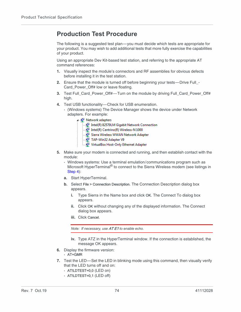
Product Technical Specification
Production Test Procedure
The following is a suggested test plan—you must decide which tests are appropriate for your product. You may wish to add additional tests that more fully exercise the capabilities of your product.
Using an appropriate Dev Kit-based test station, and referring to the appropriate AT command references:
1. Visually inspect the module’s connectors and RF assemblies for obvious defects before installing it in the test station.
2. Ensure that the module is turned off before beginning your tests—Drive Full_-Card_Power_Off# low or leave floating.
3. Test Full_Card_Power_Off#—Turn on the module by driving Full_Card_Power_Off# high.
4. Test USB functionality—Check for USB enumeration.· (Windows systems) The Device Manager shows the device under Network
adapters. For example:
5. Make sure your modem is connected and running, and then establish contact with the module:· Windows systems: Use a terminal emulation/communications program such as
Microsoft HyperTerminal® to connect to the Sierra Wireless modem (see listings in Step 4):
a. Start HyperTerminal.
b. Select File > Connection Description. The Connection Description dialog box appears.
i. Type Sierra in the Name box and click OK. The Connect To dialog box appears.
ii. Click OK without changing any of the displayed information. The Connect dialog box appears.
iii. Click Cancel.
Note: If necessary, use AT E1 to enable echo.
iv. Type ATZ in the HyperTerminal window. If the connection is established, the message OK appears.
6. Display the firmware version:· AT+GMR
7. Test the LED—Set the LED in blinking mode using this command, then visually verify that the LED turns off and on:· AT!LDTEST=0,0 (LED on)· AT!LDTEST=0,1 (LED off)
Rev. 7 Oct.19 74 41112028
Testing
8. Unlock the extended AT command set. (Note: Use AT!ENTERCND? to check command syntax, which is SKU-dependent.):· AT!ENTERCND=”<password>”
9. Put the module in diagnostic/factory test mode:· AT!DAFTMACT
10. Communicate with the SIM using +CPIN or +CIMI.When performing RF tests, use a test platform as described in Suggested Testing Equipment on page 84.
11. Test RF transmission, if desired:· (UMTS) See UMTS (WCDMA) RF Transmission Path Test on page 75.· (LTE) See LTE RF Transmission Path Test on page 77.
12. Test RF reception, if desired:· (UMTS) See UMTS (WCDMA) RF Receive Path Test on page 79.· (LTE) See LTE RF Receive Path Test on page 81.
13. Test standalone GNSS functionality—See GNSS RF Receive Path Test on page 83.
14. Drive Full_Card_Power_Off# low (or leave floating) and confirm that the module powers down:· Windows systems—The Sierra Wireless items under the Ports (COM & LPT) entry
in Device Manager disappear as the module powers off.
UMTS (WCDMA) RF Transmission Path Test
Note: This procedure segment is performed in Step 11 of the Production Test Procedure on page 74.
The suggested test procedure that follows uses the parameters in Table 3-1.
Table 3-1: Test Settings — UMTS Transmission Path
Band Frequency (MHz) Band ID Channela
a. Channel value used by the !DARCONFIG command (!DARCONFIG uses uplink (Tx) channel at the center of the corresponding band (rounded down), for both Tx and Rx testing).
2100 MHz Band 1 1950.0 9 9750
1900 MHz Band 2 1880.0 15b
b. Either 15 (WCDMA1900A) or 16 (WCDMA1900B) may be used for testing.
9400
1700 MHz Band 4 1732.6 28 1413
850 MHz Band 5 836.6 22 4183
800 MHz Band 6 835.0 22 4175
900 MHz Band 8 897.6 29 2788
1700 MHz Band 9 1767.4 31 8837
800 MHz Band 19 837.6 75 338
Rev. 7 Oct.19 75 41112028
Product Technical Specification
To test the DUT’s transmitter path:
1. Set up the power meter:
Note: This procedure describes steps using the "Power Meter: Gigatronics 8651A” (with Option 12 and Power Sensor 80701A).
a. Make sure the meter has been given sufficient time to warm up, if necessary, to enable it to take accurate measurements.
b. Zero-calibrate the meter.
c. Enable MAP mode.
2. Prepare the DUT using the following AT commands:
a. AT!ENTERCND=”<password>”(Unlock extended AT command set.)
b. AT!DAFTMACT (Enter test mode.)
c. AT!DARCONFIG=0,1,<bandValue>,<channel>(e.g. AT!DARCONFIG=0,1,2,9400)
(Set frequency band and channel.See Table 3-1 for values.)
d. AT!DAWTXCONTROL=1,<power_dBm>(e.g. AT!DAWTXCONTROL=1,10)
(Enable Tx power output.<power_dBm> = -57.0 to 23.0)
e. Take the measurement.
f. Repeat steps c–e with different Tx power levels if needed.
g. AT!DAWTXCONTROL=0 (Disable Tx power output.)
h. AT!DARCONFIGDROP=1 (Drop the current UMTS configuration.)
3. Test limits—Run ten or more good DUTs through this test procedure to obtain a nominal output power value.· Apply a tolerance of 5 to 6 dB to each measurement (assuming a good setup
design).· Monitor these limits during mass-production ramp-up to determine if further adjust-
ments are needed.
Note: The module has a nominal output power of +23 dBm 1 dB in WCDMA mode. However, the value measured by the power meter is significantly influenced (beyond the stated 1 dB output power tolerance) by the test setup (host RF cabling loss, antenna efficiency and pattern, test antenna efficiency and pattern, and choice of shield box).
Rev. 7 Oct.19 76 41112028
Testing
Note: When doing the same test over the air in an RF chamber, values are likely to be significantly lower.
LTE RF Transmission Path Test
Note: This procedure segment is performed in Step 11 of the Production Test Procedure on page 74.
The suggested test procedure that follows uses the parameters in Table 3-2..
Table 3-2: Test Settings — LTE Transmission Path
Band # Frequency (MHz) Band ID Channela
a. Channel value used by the !DARCONFIG command (!DARCONFIG uses uplink (Tx) channel at the center of the corresponding band (rounded down), for both Tx and Rx testing).
2100 MHz B1 1950.0 34 18300
1900 MHz B2 1880.0 43 18900
1800 MHz B3 1747.5 44 19575
1700 MHz B4 1732.5 42 20175
850 MHz B5 836.5 45 20525
2600 MHz B7 2535.0 35 21100
900 MHz B8 897.5 47 21625
1800 MHz B9 1767.4 48 21975
700 MHz B12 707.5 50 23095
700 MHz B13 782.0 36 23230
700 MHz B14 793.0 51 23330
850 MHz B18 822.5 54 23925
850 MHz B19 837.5 55 24075
800 MHz B20 847.0 56 24300
850 MHz B26 831.5 62 26865
2500 MHz B41 2593.0 76 40620
3500 MHz B42 3500.0 77 42590
3700 MHz B43 3700.0 88 44590
3600 MHz B48 3625.0 96 55990
1700 MHz B66 1745.0 83 132322
Rev. 7 Oct.19 77 41112028
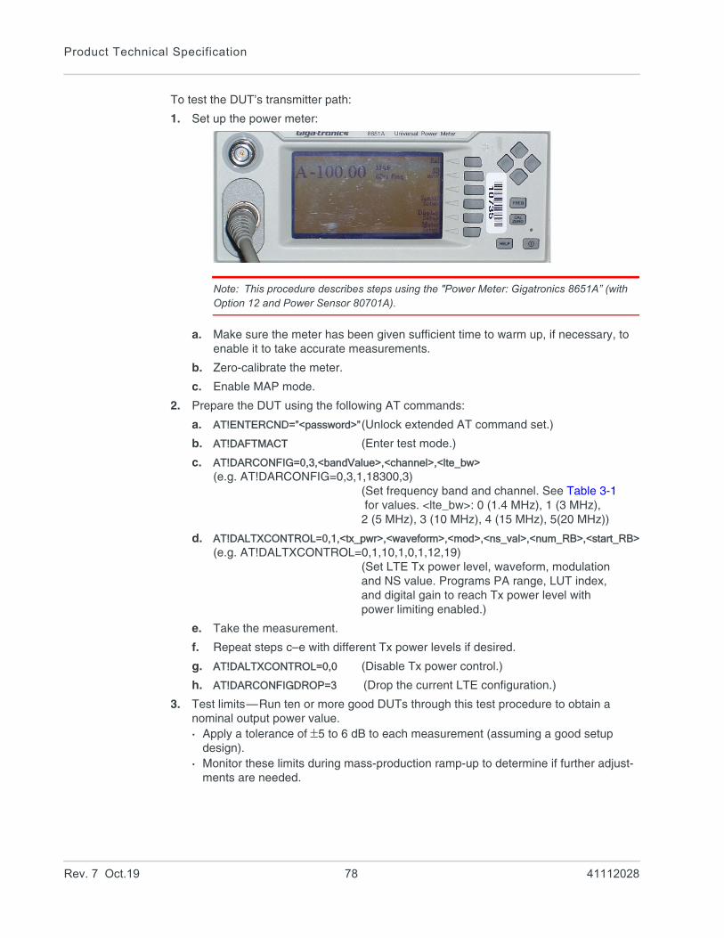
Product Technical Specification
To test the DUT’s transmitter path:
1. Set up the power meter:
Note: This procedure describes steps using the "Power Meter: Gigatronics 8651A” (with Option 12 and Power Sensor 80701A).
a. Make sure the meter has been given sufficient time to warm up, if necessary, to enable it to take accurate measurements.
b. Zero-calibrate the meter.
c. Enable MAP mode.
2. Prepare the DUT using the following AT commands:
a. AT!ENTERCND=”<password>”(Unlock extended AT command set.)
b. AT!DAFTMACT (Enter test mode.)
c. AT!DARCONFIG=0,3,<bandValue>,<channel>,<lte_bw>(e.g. AT!DARCONFIG=0,3,1,18300,3)
(Set frequency band and channel. See Table 3-1 for values. <lte_bw>: 0 (1.4 MHz), 1 (3 MHz),2 (5 MHz), 3 (10 MHz), 4 (15 MHz), 5(20 MHz))
d. AT!DALTXCONTROL=0,1,<tx_pwr>,<waveform>,<mod>,<ns_val>,<num_RB>,<start_RB>(e.g. AT!DALTXCONTROL=0,1,10,1,0,1,12,19)
(Set LTE Tx power level, waveform, modulationand NS value. Programs PA range, LUT index,and digital gain to reach Tx power level withpower limiting enabled.)
e. Take the measurement.
f. Repeat steps c–e with different Tx power levels if desired.
g. AT!DALTXCONTROL=0,0 (Disable Tx power control.)
h. AT!DARCONFIGDROP=3 (Drop the current LTE configuration.)
3. Test limits—Run ten or more good DUTs through this test procedure to obtain a nominal output power value.· Apply a tolerance of 5 to 6 dB to each measurement (assuming a good setup
design).· Monitor these limits during mass-production ramp-up to determine if further adjust-
ments are needed.
Rev. 7 Oct.19 78 41112028
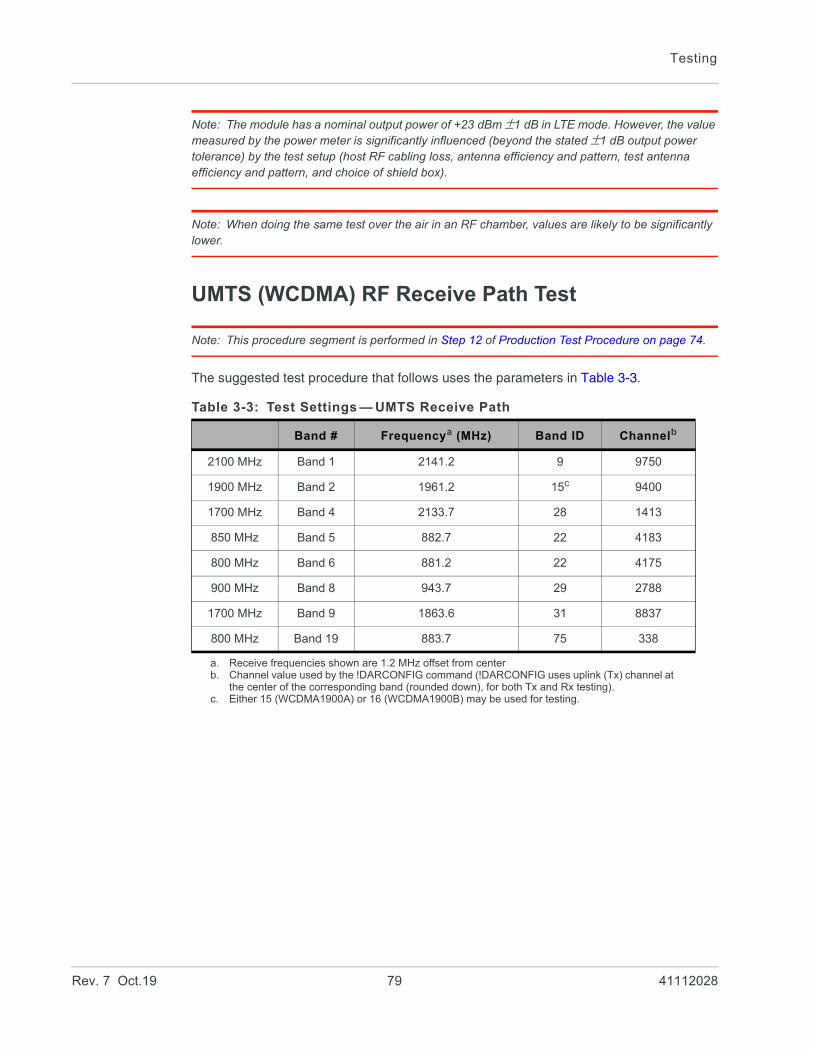
Testing
Note: The module has a nominal output power of +23 dBm 1 dB in LTE mode. However, the value measured by the power meter is significantly influenced (beyond the stated 1 dB output power tolerance) by the test setup (host RF cabling loss, antenna efficiency and pattern, test antenna efficiency and pattern, and choice of shield box).
Note: When doing the same test over the air in an RF chamber, values are likely to be significantly lower.
UMTS (WCDMA) RF Receive Path Test
Note: This procedure segment is performed in Step 12 of Production Test Procedure on page 74.
The suggested test procedure that follows uses the parameters in Table 3-3.
Table 3-3: Test Settings — UMTS Receive Path
Band # Frequencya (MHz)
a. Receive frequencies shown are 1.2 MHz offset from center
Band ID Channelb
b. Channel value used by the !DARCONFIG command (!DARCONFIG uses uplink (Tx) channel at the center of the corresponding band (rounded down), for both Tx and Rx testing).
2100 MHz Band 1 2141.2 9 9750
1900 MHz Band 2 1961.2 15c
c. Either 15 (WCDMA1900A) or 16 (WCDMA1900B) may be used for testing.
9400
1700 MHz Band 4 2133.7 28 1413
850 MHz Band 5 882.7 22 4183
800 MHz Band 6 881.2 22 4175
900 MHz Band 8 943.7 29 2788
1700 MHz Band 9 1863.6 31 8837
800 MHz Band 19 883.7 75 338
Rev. 7 Oct.19 79 41112028
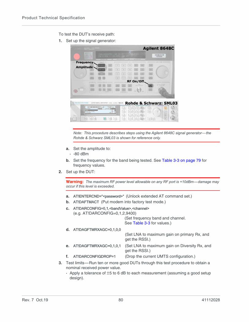
Product Technical Specification
To test the DUT’s receive path:
1. Set up the signal generator:
Note: This procedure describes steps using the Agilent 8648C signal generator—the Rohde & Schwarz SML03 is shown for reference only.
a. Set the amplitude to:· -80 dBm
b. Set the frequency for the band being tested. See Table 3-3 on page 79 for frequency values.
2. Set up the DUT:
Warning: The maximum RF power level allowable on any RF port is +10dBm—damage may occur if this level is exceeded.
a. AT!ENTERCND=”<password>” (Unlock extended AT command set.)b. AT!DAFTMACT (Put modem into factory test mode.)
c. AT!DARCONFIG=0,1,<bandValue>,<channel>(e.g. AT!DARCONFIG=0,1,2,9400)
(Set frequency band and channel.See Table 3-3 for values.)
d. AT!DAGFTMRXAGC=0,1,0,0 (Set LNA to maximum gain on primary Rx, andget the RSSI.)
e. AT!DAGFTMRXAGC=0,1,0,1 (Set LNA to maximum gain on Diversity Rx, andget the RSSI.)
f. AT!DARCONFIGDROP=1 (Drop the current UMTS configuration.)
3. Test limits—Run ten or more good DUTs through this test procedure to obtain a nominal received power value.· Apply a tolerance of 5 to 6 dB to each measurement (assuming a good setup
design).
Rev. 7 Oct.19 80 41112028
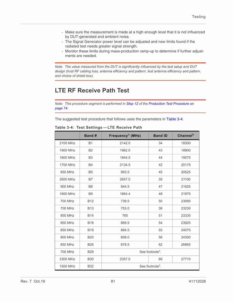
Testing
· Make sure the measurement is made at a high enough level that it is not influenced by DUT-generated and ambient noise.
· The Signal Generator power level can be adjusted and new limits found if the radiated test needs greater signal strength.
· Monitor these limits during mass-production ramp-up to determine if further adjust-ments are needed.
Note: The value measured from the DUT is significantly influenced by the test setup and DUT design (host RF cabling loss, antenna efficiency and pattern, test antenna efficiency and pattern, and choice of shield box).
LTE RF Receive Path Test
Note: This procedure segment is performed in Step 12 of the Production Test Procedure on page 74.
The suggested test procedure that follows uses the parameters in Table 3-4.
Table 3-4: Test Settings — LTE Receive Path
Band # Frequencya (MHz) Band ID Channelb
2100 MHz B1 2142.0 34 18300
1900 MHz B2 1962.0 43 18900
1800 MHz B3 1844.5 44 19575
1700 MHz B4 2134.5 42 20175
850 MHz B5 883.5 45 20525
2600 MHz B7 2657.0 35 21100
900 MHz B8 944.5 47 21625
1800 MHz B9 1864.4 48 21975
700 MHz B12 739.5 50 23095
700 MHz B13 753.0 36 23230
850 MHz B14 765 51 23330
850 MHz B18 869.5 54 23925
850 MHz B19 884.5 55 24075
800 MHz B20 808.0 56 24300
850 MHz B26 878.5 62 26865
700 MHz B29 See footnotec.
2300 MHz B30 2357.0 66 27710
1500 MHz B32 See footnotec.
Rev. 7 Oct.19 81 41112028
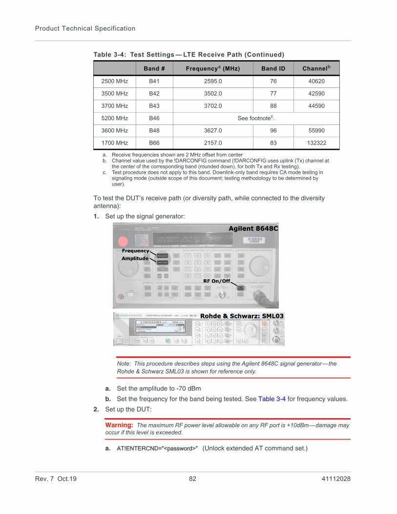
Product Technical Specification
To test the DUT’s receive path (or diversity path, while connected to the diversity antenna):
1. Set up the signal generator:
Note: This procedure describes steps using the Agilent 8648C signal generator—the Rohde & Schwarz SML03 is shown for reference only.
a. Set the amplitude to -70 dBm
b. Set the frequency for the band being tested. See Table 3-4 for frequency values.
2. Set up the DUT:
Warning: The maximum RF power level allowable on any RF port is +10dBm—damage may occur if this level is exceeded.
a. AT!ENTERCND=”<password>” (Unlock extended AT command set.)
2500 MHz B41 2595.0 76 40620
3500 MHz B42 3502.0 77 42590
3700 MHz B43 3702.0 88 44590
5200 MHz B46 See footnotec.
3600 MHz B48 3627.0 96 55990
1700 MHz B66 2157.0 83 132322
a. Receive frequencies shown are 2 MHz offset from centerb. Channel value used by the !DARCONFIG command (!DARCONFIG uses uplink (Tx) channel at
the center of the corresponding band (rounded down), for both Tx and Rx testing).c. Test procedure does not apply to this band. Downlink-only band requires CA mode testing in
signaling mode (outside scope of this document; testing methodology to be determined by user).
Table 3-4: Test Settings — LTE Receive Path (Continued)
Band # Frequencya (MHz) Band ID Channelb
Rev. 7 Oct.19 82 41112028
Testing
b. AT!DAFTMACT (Put modem into factory test mode.)c. AT!DARCONFIG=0,3,<bandValue>,<channel>,<lte_bw>
(e.g. AT!DARCONFIG=0,3,1,18300,3)(Set frequency band and channel. See Table 3-4 for values. <lte_bw>: 0 (1.4 MHz), 1 (3 MHz),2 (5 MHz), 3 (10 MHz), 4 (15 MHz), 5(20 MHz))
d. AT!DAGFTMRXAGC=0,3,0,0 (Set LNA to maximum gain on primary Rx, andget the RSSI.)
e. AT!DAGFTMRXAGC=0,3,0,1 (Set the LNA to maximum gain on Diversity Rx,and get the RSSI.)
f. AT!DARCONFIGDROP=0,3 (Drop the current LTE configuration.)
3. Test limits—Run ten or more good DUTs through this test procedure to obtain a nominal received power value.· Apply a tolerance of 5 to 6 dB to each measurement (assuming a good setup
design).· Make sure the measurement is made at a high enough level that it is not influenced
by DUT-generated and ambient noise.· The Signal Generator power level can be adjusted and new limits found if the
radiated test needs greater signal strength.· Monitor these limits during mass-production ramp-up to determine if further adjust-
ments are needed.
Note: The value measured from the DUT is significantly influenced by the test setup and DUT design (host RF cabling loss, antenna efficiency and pattern, test antenna efficiency and pattern, and choice of shield box).
GNSS RF Receive Path Test
The GNSS receive path uses either the dedicated GNSS connector or the shared Diversity/MIMO/GNSS connector.
To test the GNSS receive path:
1. Inject a carrier signal at -110dBm, frequency 1575.52 MHz into the GNSS Rx path at the connector. (Note that this frequency is 100 kHz higher than the actual GPS L1 center frequency.)
2. Test the signal carrier-to-noise level at the GNSS receiver:
a. AT!ENTERCND=”<password>” (Unlock extended AT command set.)
b. AT!DAFTMACT (Put modem into factory test mode.)
c. AT!DACGPSTESTMODE=1 (Start CGPS diagnostic task.)
d. AT!DACGPSSTANDALONE=1 (Enter standalone RF mode.)
e. AT!DACGPSMASKON (Enable log mask.)
f. AT!DACGPSCTON (Return signal-to-noise and frequency measurements.)
g. Repeat AT!DACGPSCTON five to ten times to ensure the measurements are repeatable and stable.
3. Leave the RF connection to the embedded module intact, and turn off the signal generator.
Rev. 7 Oct.19 83 41112028
Product Technical Specification
4. Take several more !DACGPSCTON readings. This will demonstrate a 'bad' signal in order to set limits for testing, if needed. This frequency offset should fall outside of the guidelines in the note below, which indicates that the CtoN result is invalid.
5. (Optional) Turn the signal generator on again, and reduce the level to -120dBm. Take more !DACGPSCTON readings and use these as a reference for what a marginal/poor signal would be.
Note: The response to AT!DACGPSCTON for a good connection should show CtoN within 58 +/- 5dB and Freq (frequency offset) within 100000 Hz +/- 5000 Hz .
Quality Assurance Testing
Note: QA is an ongoing process based on random samples from a finished batch of devices.
The quality assurance tests that you perform on your finished products should be designed to verify the performance and quality of your devices.
The following are some testing suggestions that can confirm that the antenna is interfaced properly, and that the RF module is calibrated and performs to specifications:• Module registration on cellular networks• Power consumption• Originate and terminate data and voice (if applicable) calls• Cell hand-off• Transmitter and receiver tests• FER (Frame Error Rate) as an indicator of receiver sensitivity/performance• Channel and average power measurements to verify that the device is transmitting
within product specifications• RF sensitivity tests• RF sensitivity testing—BER/BLER for different bands and modes• Transmitter and receiver tests (based on relevant sections of the 3GPP TS51010 and
3GPP 34121 documents)
Suggested Testing EquipmentTo perform production and post-production tests, you will require appropriate testing equipment. A test computer can be used to coordinate testing between the integrated module (on the development kit or host) and the measurement equipment, usually with GPIB connections. The suggested setup includes a power meter to test RF output power and a signal generator to evaluate the receiver.
Testing Assistance Provided by Sierra Wireless
Extended AT commands have been implemented to assist with performing FTA GCF tests and portions of CE Mark tests requiring radio module access. These are documented in the [2] AirPrime EM75xx AT Command Reference (Doc# 41111748).
Sierra Wireless offers optional professional services based assistance to OEMs with regulatory approvals.
Rev. 7 Oct.19 84 41112028
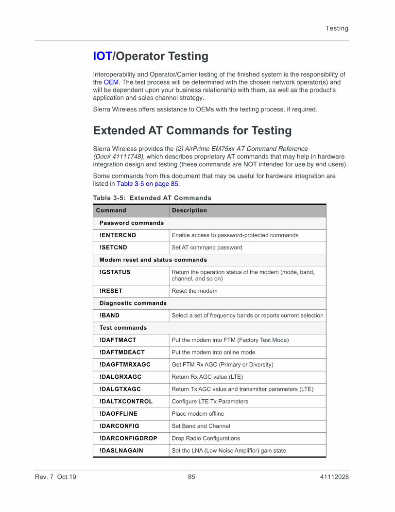
Testing
IOT/Operator Testing
Interoperability and Operator/Carrier testing of the finished system is the responsibility of the OEM. The test process will be determined with the chosen network operator(s) and will be dependent upon your business relationship with them, as well as the product's application and sales channel strategy.
Sierra Wireless offers assistance to OEMs with the testing process, if required.
Extended AT Commands for Testing
Sierra Wireless provides the [2] AirPrime EM75xx AT Command Reference (Doc# 41111748), which describes proprietary AT commands that may help in hardware integration design and testing (these commands are NOT intended for use by end users).
Some commands from this document that may be useful for hardware integration are listed in Table 3-5 on page 85.
Table 3-5: Extended AT Commands
Command Description
Password commands
!ENTERCND Enable access to password-protected commands
!SETCND Set AT command password
Modem reset and status commands
!GSTATUS Return the operation status of the modem (mode, band, channel, and so on)
!RESET Reset the modem
Diagnostic commands
!BAND Select a set of frequency bands or reports current selection
Test commands
!DAFTMACT Put the modem into FTM (Factory Test Mode)
!DAFTMDEACT Put the modem into online mode
!DAGFTMRXAGC Get FTM Rx AGC (Primary or Diversity)
!DALGRXAGC Return Rx AGC value (LTE)
!DALGTXAGC Return Tx AGC value and transmitter parameters (LTE)
!DALTXCONTROL Configure LTE Tx Parameters
!DAOFFLINE Place modem offline
!DARCONFIG Set Band and Channel
!DARCONFIGDROP Drop Radio Configurations
!DASLNAGAIN Set the LNA (Low Noise Amplifier) gain state
Rev. 7 Oct.19 85 41112028
Product Technical Specification
!DAWGAVGAGC Return averaged RX AGC value (WCDMA)
!DAWINFO Return WCDMA mode RF information
!DAWTXCONTROL Configure WCDMA Tx Power
Table 3-5: Extended AT Commands
Command Description
Rev. 7 Oct.19 86 41112028
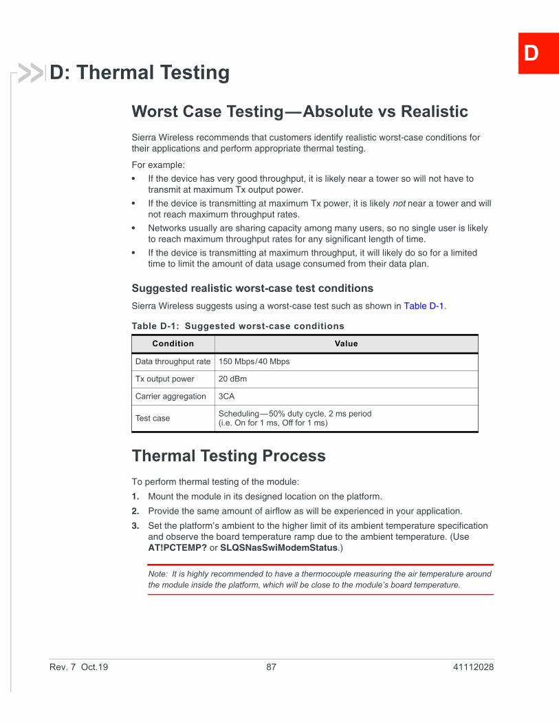
D
D: Thermal TestingWorst Case Testing—Absolute vs Realistic
Sierra Wireless recommends that customers identify realistic worst-case conditions for their applications and perform appropriate thermal testing.
For example:
• If the device has very good throughput, it is likely near a tower so will not have to transmit at maximum Tx output power.
• If the device is transmitting at maximum Tx power, it is likely not near a tower and will not reach maximum throughput rates.
• Networks usually are sharing capacity among many users, so no single user is likely to reach maximum throughput rates for any significant length of time.
• If the device is transmitting at maximum throughput, it will likely do so for a limited time to limit the amount of data usage consumed from their data plan.
Suggested realistic worst-case test conditions
Sierra Wireless suggests using a worst-case test such as shown in Table D-1.
Thermal Testing Process
To perform thermal testing of the module:
1. Mount the module in its designed location on the platform.
2. Provide the same amount of airflow as will be experienced in your application.
3. Set the platform’s ambient to the higher limit of its ambient temperature specification and observe the board temperature ramp due to the ambient temperature. (Use AT!PCTEMP? or SLQSNasSwiModemStatus.)
Note: It is highly recommended to have a thermocouple measuring the air temperature around the module inside the platform, which will be close to the module’s board temperature.
Table D-1: Suggested worst-case conditions
Condition Value
Data throughput rate 150 Mbps/40 Mbps
Tx output power 20 dBm
Carrier aggregation 3CA
Test caseScheduling—50% duty cycle, 2 ms period(i.e. On for 1 ms, Off for 1 ms)
Rev. 7 Oct.19 87 41112028
Product Technical Specification
4. Set up a call with the use case for the platform (throughput rate, output power, duty cycle) on the worst-case band.
Note: The worst case band for power consumption and thermals is a 3CA call with PCC LTE Band 66 (20 MHz) and SCC any bands (20 MHz + 20 MHz). For example, Sierra Wireless tests using B66+B2+B66.
5. Observe the ramp in board temperature due to the call, and confirm whether the overall system performance still meets customer requirements.
6. Use AT!TMSTATUS? to check the module’s thermal mitigation status (see [2] AirPrime EM75xx AT Command Reference (Doc# 41111748) for details).
7. Increase the platform’s ambient temperature to determine the margin that exists over the desired temperature specifications as subsequent mitigation methods activate (e.g. UL data rate throttled, DL throughput throttled (third and second CA dropped), UL power reduced, Emergency Service).
Rev. 7 Oct.19 88 41112028
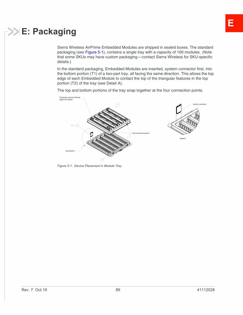
E
E: PackagingSierra Wireless AirPrime Embedded Modules are shipped in sealed boxes. The standard packaging (see Figure 5-1), contains a single tray with a capacity of 100 modules. (Note that some SKUs may have custom packaging—contact Sierra Wireless for SKU-specific details.)
In the standard packaging, Embedded Modules are inserted, system connector first, into the bottom portion (T1) of a two-part tray. all facing the same direction. This allows the top edge of each Embedded Module to contact the top of the triangular features in the top portion (T2) of the tray (see Detail A).
The top and bottom portions of the tray snap together at the four connection points.
Figure 5-1: Device Placement in Module Tray
Triangular recesses hold top
edges of modules
Tray connection points
See Detail A
Detail A
System connector
Rev. 7 Oct.19 89 41112028
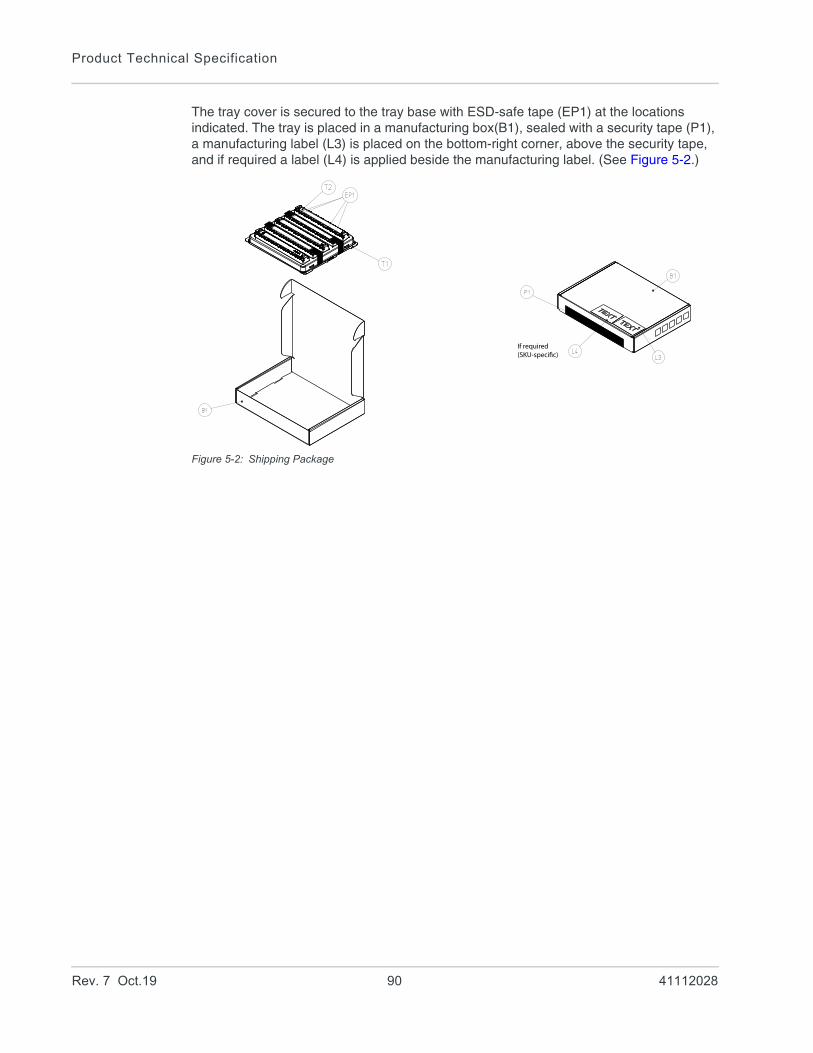
Product Technical Specification
The tray cover is secured to the tray base with ESD-safe tape (EP1) at the locations indicated. The tray is placed in a manufacturing box(B1), sealed with a security tape (P1), a manufacturing label (L3) is placed on the bottom-right corner, above the security tape, and if required a label (L4) is applied beside the manufacturing label. (See Figure 5-2.)
Figure 5-2: Shipping Package
If required
(SKU-specific)
Rev. 7 Oct.19 90 41112028
Rev. 7 Oct.19 91 41112028
FF: References
This guide deals specifically with hardware integration issues that are unique to AirPrime embedded modules.
Sierra Wireless Documents
The Sierra Wireless documents listed below are available from www.sierrawireless.com. For additional documents describing embedded module design, usage, and integration issues, contact your Sierra Wireless account representative.
Command Documents
[1] AT Command Set for User Equipment (UE) (Release 6) (Doc# 3GPP TS 27.007)
[2] AirPrime EM75xx AT Command Reference (Doc# 41111748)
Other Sierra Documents
[3] M.2 Dev Kit Welcome Letter (Doc# 2400323)
[4] AirCard/AirPrime USB Driver Developer’s Guide (Doc# 2130634)
Industry/Other Documents
The following non-Sierra Wireless references are not included in your documentation package:
[5] FCC Regulations - Part 15 - Radio Frequency Devices
[6] IEC-61000-4-2 level 3 (Electrostatic Discharge Immunity Test)
[7] Mobile Station (MS) Conformance Specification; Part 4: Subscriber Interface Module (Doc# 3GPP TS 11.10-4)
[8] PCI Express NGFF (M.2) Electromechanical Specification Revision 1.0
[9] Universal Serial Bus Specification, Rev 2.0
[10] Universal Serial Bus Specification, Rev 3.0
[11] JESD22-A114-B
[12] JESD22-C101
[13]MIPI Alliance Specification for RF Front-End Control Interface
Rev 7 Oct
G
T
G: Acronyms
able G-1: Acronyms and Definitions
Acronym or term Definition
3GPP 3rd Generation Partnership Project
8PSK Octagonal Phase Shift Keying
AGC Automatic Gain Control
A-GPS Assisted GPS
API Application Programming Interface
BeiDou BeiDou Navigation Satellite System
A Chinese system that uses a series of satellites in geostationary and middle earth orbits to provide navigational data.
BER Bit Error Rate—A measure of receive sensitivity
BLER Block Error Rate
bluetooth Wireless protocol for data exchange over short distances
CQI Channel Quality Indication
COM Communication port
CS Circuit-switched
CSG Closed Subscriber Group
CW Continuous waveform
dB Decibel = 10 x log10 (P1/P2)P1 is calculated power; P2 is reference power
Decibel = 20 x log10 (V1/V2)V1 is calculated voltage, V2 is reference voltage
dBm A logarithmic (base 10) measure of relative power (dB for decibels); relative to milliwatts (m). A dBm value will be 30 units (1000 times) larger (less negative) than a dBW value, because of the difference in scale (milliwatts vs. watts).
DC-HSPA+ Dual Carrier HSPA+
DCS Digital Cellular System
A cellular communication infrastructure that uses the 1.8 GHz radio spectrum.
DL Downlink (network to mobile)
DRX Discontinuous Reception
DSM Distributed Shared Memory
DUT Device Under Test
eICIC Enhanced Inter-Cell Interference Coordination
EIRP Effective (or Equivalent) Isotropic Radiated Power
.19 92 41112028
Acronyms
EMC Electromagnetic Compatibility
EMI Electromagnetic Interference
ERP Effective Radiated Power
ESD Electrostatic Discharge
FCC Federal Communications Commission
The U.S. federal agency that is responsible for interstate and foreign communications. The FCC regulates commercial and private radio spectrum management, sets rates for communications services, determines standards for equipment, and controls broadcast licensing. Consult www.fcc.gov.
FDD Frequency Division Duplexing
FDMA Frequency Division Multiple Access
feICIC Further Enhanced Inter-Cell Interference Coordination
FER Frame Error Rate—A measure of receive sensitivity.
firmware Software stored in ROM or EEPROM; essential programs that remain even when the system is turned off. Firmware is easier to change than hardware but more permanent than software stored on disk.
FOTA Firmware Over The Air—Technology used to download firmware upgrades directly from the service provider, over the air.
FOV Field Of View
FSN Factory Serial Number—A unique serial number assigned to the mini card during manufacturing.
Galileo A European system that uses a series of satellites in middle earth orbit to provide navigational data.
GCF Global Certification Forum
GLONASS Global Navigation Satellite System—A Russian system that uses a series of 24 satellites in middle circular orbit to provide navigational data.
GMSK Gaussian Minimum Shift Keying modulation
GNSS Global Navigation Satellite Systems (GPS, GLONASS, BeiDou, and Galileo)
GPS Global Positioning System
An American system that uses a series of 24 satellites in middle circular orbit to provide navigational data.
Host The device into which an embedded module is integrated
HSDPA High Speed Downlink Packet Access
HSPA+ Enhanced HSPA, as defined in 3GPP Release 7 and beyond
HSUPA High Speed Uplink Packet Access
Hz Hertz = 1 cycle/second
Table G-1: Acronyms and Definitions (Continued)
Acronym or term Definition
Rev 7 Oct.19 93 41112028
Product Technical Specification
IC Industry Canada
IF Intermediate Frequency
IMEI International Mobile Equipment Identity
IMS IP Multimedia Subsystem—Architectural framework for delivering IP multimedia services.
inrush current Peak current drawn when a device is connected or powered on
inter-RAT Radio Access Technology
IOT Interoperability Testing
IS Interim Standard.
After receiving industry consensus, the TIA forwards the standard to ANSI for approval.
ISIM IMS Subscriber Identity Module (Also referred to as a SIM card)
LED Light Emitting Diode.
A semiconductor diode that emits visible or infrared light.
LHCP Left-Hand Circular Polarized
LNA Low Noise Amplifier
LPM Low Power Mode
LPT Line Print Terminal
LTE Long Term Evolution—a high-performance air interface for cellular mobile communication systems.
MCS Modulation and Coding Scheme
MHz Megahertz = 10e6 Hz
MIMO Multiple Input Multiple Output—wireless antenna technology that uses multiple antennas at both transmitter and receiver side. This improves performance.
NAS/AS Network Access Server
NC No Connect
NIC Network Interface Card
NLIC Non-Linear Interference Cancellation
NMEA National Marine Electronics Association
OEM Original Equipment Manufacturer—a company that manufactures a product and sells it to a reseller.
OFDMA Orthogonal Frequency Division Multiple Access
OMA DM Open Mobile Alliance Device Management—A device management protocol.
OTA ‘Over the air’ (or radiated through the antenna)
Table G-1: Acronyms and Definitions (Continued)
Acronym or term Definition
Rev 7 Oct.19 94 41112028
Acronyms
PA Power Amplifier
packet A short, fixed-length block of data, including a header, that is transmitted as a unit in a communications network.
PCB Printed Circuit Board
PCC Primary Component Carrier
PCS Personal Communication System
A cellular communication infrastructure that uses the 1.9 GHz radio spectrum.
PDN Packet Data Network
PMI Pre-coding Matrix Index
PSS Primary synchronisation signal
PST Product Support Tools
PTCRB PCS Type Certification Review Board
QAM Quadrature Amplitude Modulation.
This form of modulation uses amplitude, frequency, and phase to transfer data on the carrier wave.
QCI QoS Class Identifier
QMI Qualcomm MSM/Modem Interface
QOS Quality of Service
QPSK Quadrature Phase-Shift Keying
QPST Qualcomm Product Support Tools
QZSS Quasi-Zenith Satellite System—Japanese system for satellite-based augmentation of GPS.
RAT Radio Access Technology
RF Radio Frequency
RI Ring Indicator
roaming A cellular subscriber is in an area where service is obtained from a cellular service provider that is not the subscriber’s provider.
RSE Radiated Spurious Emissions
RSSI Received Signal Strength Indication
SCC Secondary Component Carrier
SDK Software Development Kit
SED Smart Error Detection
Sensitivity (Audio) Measure of lowest power signal that the receiver can measure.
Table G-1: Acronyms and Definitions (Continued)
Acronym or term Definition
Rev 7 Oct.19 95 41112028
Product Technical Specification
Sensitivity (RF) Measure of lowest power signal at the receiver input that can provide a prescribed BER/BLER/SNR value at the receiver output.
SG An LTE signaling interface for SMS (“SMS over SGs”)
SIB System Information Block
SIM Subscriber Identity Module. Also referred to as USIM or UICC.
SIMO Single Input Multiple Output—smart antenna technology that uses a single antenna at the transmitter side and multiple antennas at the receiver side. This improves performance and security.
SISO Single Input Single Output—antenna technology that uses a single antenna at both the transmitter side and the receiver side.
SKU Stock Keeping Unit—identifies an inventory item: a unique code, consisting of numbers or letters and numbers, assigned to a product by a retailer for purposes of identification and inventory control.
SMS Short Message Service.
A feature that allows users of a wireless device on a wireless network to receive or transmit short electronic alphanumeric messages (up to 160 characters, depending on the service provider).
S/N Signal-to-noise (ratio)
SNR Signal-to-Noise Ratio
SOF Start of Frame—A USB function.
SSS Secondary synchronisation signal.
SUPL Secure User Plane Location
TDD Time Division Duplexing
TD-SCDMA Time Division Synchronous Code Division Multiple Access
TIA/EIA Telecommunications Industry Association / Electronics Industry Association.A standards setting trade organization, whose members provide communications and information technology products, systems, distribution services and professional services in the United States and around the world. Consult www.tiaonline.org.
TIS Total Isotropic Sensitivity
TRP Total Radiated Power
UDK Universal Development Kit (for PCI Express Mini Cards)
UE User Equipment
UICC Universal Integrated Circuit Card (Also referred to as a SIM card.)
UL Uplink (mobile to network)
UMTS Universal Mobile Telecommunications System
USB Universal Serial Bus
Table G-1: Acronyms and Definitions (Continued)
Acronym or term Definition
Rev 7 Oct.19 96 41112028
Acronyms
USIM Universal Subscriber Identity Module (UMTS)
VCC Supply voltage
VSWR Voltage Standing Wave Ratio
WAN Wide Area Network
WCDMA Wideband Code Division Multiple Access (also referred to as UMTS)
WLAN Wireless Local Area Network
ZIF Zero Intermediate Frequency
ZUC ZUC stream cypher
Table G-1: Acronyms and Definitions (Continued)
Acronym or term Definition
Rev 7 Oct.19 97 41112028
Re
Index
Numerics3D gain, averagegain
3D average (GNSS), 673GPP compliance
LTE, 62UMTS, 62
A
acceptance tests, 71accessories, 17accuracy (GNSS), 47acquisition time (GNSS), 47acronyms and definitions, 92– 97A-GNSS, 17A-GPS, 17antenna
connection considerations, 37connectors, 19control, 19, 36custom, design, 38diversity antenna, disabling, 38GNSS, specifications, recommended, 65, 67limit, matching coaxial connections, 37location, considerations, 38matching, considerations, 38maximum cable loss, 37routing, 38specification, 65– 68specifications, recommended, 65testing, 67
antennasdesign checklist, 69
API, 56application interface features, 15approvals, regulatory and industry, 62AT commands, 85averaged call mode DC power consumption, 49averaged standby DC power consumption, 48
B
bands supported, RFsummary, 12LTE, 42, 43, 75, 77, 79, 81
bearers, dedicated, 16BER (Bit Error Rate), 41bit error rate (BER)
measure of sensitivity, 41block diagram
expanded RF, 21, 22system, 20
bottom view, 58
C
cable lossantenna, maximum, 37
capacitorswith SIM, 32with XIM_DATA / XIM_CLK, 31
carrier/operator testing, 85cell selection, 16certification tests, 72checklist, design, 69communications, host to modem
design checklist, 70conducted Tx power tolerances, 46connection
grounding, 39connectors, required
host-module, 17control interface, 32CQI, 16
D
DC power consumptionaveraged call mode, 49averaged standby, 48
desense. See RFdesign checklist
antennas, 69component placement, 69EMI/ESD, 69host/modem communications, 70power, 69thermal, 70USB3, 69
detach procedure, 16dimensioned view, 58dimensions, 57, 58diversity antenna
disabling, 38drop specifications, 57dynamic power control, 19
E
EDGEconnector, required, 18
electrical specifications, 19electrostatic discharge specifications, 57electrostatic discharge. See ESDenvelope correlation coefficient, 66environmental specifications, 57– 59ESD
design checklist, 69protection requirements, 59
ESD specifications, 57expanded RF block diagram, 21, 22
F
field of view, 67filtering, RF desense, 40form factor, 57FOV, 67free space average gain, 67
v 7 Oct.19 98 41112028
Index
frequencies supported, 41frequency band support
LTE, 42, 43, 75, 77, 79, 81Full_Card_Power_Off#, 34
G
gainGNSS, 67maximum, 62, 66mean effective, 66mean effective imbalance, 66
GNSSantenna specifications, recommended, 65, 67
GPSfeatures supported, 17specifications, 47
GPS_DISABLE#, 19, 32, 33ground specifications, 27grounding
connection considerations, 39
H
host interfacepin assignments, 22
humidity specifications, 57
I
I/O rise time requirements, 31impedance
module–antenna, 38SIM, 31
industry approvals, 62integration requirements, 18interface
control interface, 32feature summary, 15host, pin assignments, 22QMI, 56SIM, 29software, 56USB, 28
interferencedevice generated, 40host-generated, 40power supply noise, 54wireless devices, 39
Interoperability testing, 85intra-LTE mobility, 16IOT testing, 85iRAT, 16isolation, 66, 67
L
labeling, 59LED
example, 36LED output, 19, 32, 35
LTE3GPP compliance, 62bandwidth support, 42features, 16frequency band support, 42, 43, 75, 77, 79, 81
M
mean effective gain, 66mean effective gain imbalance, 66mechanical specifications, 57– 59MIB, 16modem features, 16module
power states, 50– 52
N
NAS/AS security, 16noise
leakage, minimizing, 39RF interference, power supply, 54
O
OEMassistance with testing, 85labeling, 59
operator/carrier testing, 85ordering information, 18
P
packaging, 89paging procedures, 16PCB
multi-layer, shielding for RF desense, 40PDN connections, multiple, 16pin assignments, host interface, 22PMI, 16polarization, 67position location, 17power
design checklist, 69handling, 66power-up timing, 53ramp-up timing, 52state machines, 51states, module, 50– 52supply, RF interference, 54supply, ripple limit, 54
power consumption, DCaveraged call mode, 49averaged standby, 48
power off signal, 19power specifications, 27power tolerances, conducted Tx, 46Product Support Tool, QUALCOMM (QPST), 56production tests, 73PSS, 16
Rev 7 Oct.19 99 41112028
Product Technical Specification
Q
QMI interface, 56QPST (QUALCOMM Product Support Tool), 56QUALCOMM Product Support Tool (QPST), 56quality assurance tests, 84QXDM support, 56
R
radiated efficiency, total, 65radiated sensitivity measurement, 41radiated spurious emissions, 40radiation patterns, 66references, 91regulatory approvals, 62regulatory information, ??– 64
FCC, 62reset
timing, 53RESET#, 19, 34resistors, external pull-up, 31RF
antenna cable loss, maximum, 37antenna connection, considerations, 37connectors, required, 17desense
device-generated, 40harmonic energy, filtering, 40mitigation suggestions, 40shielding suggestions, 40
interferenceother devices, 40power supply, 54wireless devices, 39
RF bands supportedsummary, 12LTE, 42, 43, 75, 77, 79, 81
RF block diagram, expanded, 21, 22RF specifications, 37–??RI, 16RSE, 40Rx sensitivity
conducted, 45, 46
S
salesordering, 18
SAR backoff, 55SDKs available, 56SED
see Smart Error DetectionSee also GPS_DISABLE#, 33See also W_DISABLE#, 33sensitivity
conducted, RF parameter, 45, 46defined, 41radiated measurement, overview, 41testing, overview, 41
shieldingmodule, compliance, 37reducing RF desense, 40
shock specifications, 57SIB, 16signals, 32
Full_Card_Power_Off#, 34RESET#, 34WWAN_LED#, 35
SIMcapacitor recommendations, 32card contacts, 28, 31clock rate, 31connector, required, 18electrical specifications, 31impedance, connectors, 31interface, 29interface diagram, 30operation, 31– 32
SIM Detect, 19Smart Error Detection
detecting module reset, 55SMS features, 17Snow 3G/AES security, 16software interface, 56specifications
electrical, 19environmental specifications, 57– 59GPS, 47mechanical, 57– 59RF, 37–??
SSS, 16standalone mode, GPS/GLONASS, 17standby DC power consumption, averaged, 48state machines, 51support
testing assistance by Sierra Wireless, 84tools, 56
system acquisition, 16system block diagram, 20
T
temperature specifications, 57temperature, module. See thermaltesting
overview, 71acceptance tests, 71assistance provided by Sierra Wireless, 84certification tests, 72equipment, suggested, 84interoperability and operator/carrier testing, 85manual functional test, suggested, 73production tests, 73quality assurance tests, 84RF receive path, LTE, 81RF receive path, UMTS, 79RF transmission path, LTE, 77RF transmission path, UMTS, 75suggestions, 71–??
Rev 7 Oct.19 100 41112028
Index
thermalconsiderations, 60– 61design checklist, 70dissipation, factors affecting, 60dissipation, suggestions, 61testing, module, 61
timingpower ramp-up, 52power-up, 53reset, 53USB enumeration, 53
top view, 58tracking session
automatic, 17standalone, 17
Tx power tolerances, conducted, 46
U
UMTS3GPP compliance, 62
USBdrivers, user-developed, 29high / full speed throughput performance, 29interface, 28
USB enumeration timing, 53USB3
design checklist, 69
V
vibration specifications, 57VSWR, 65, 67
W
W_DISABLE#, 19, 32, 33WAKE_ON_WAN#, 19Wireless Disable, 32Wireless Disable (GNSS), 33Wireless Disable (Main RF), 33WWAN_LED#, 32, 35
Z
ZIF (Zero Intermediate Frequency), 39
Rev 7 Oct.19 101 41112028