Embed Size (px)
Citation preview

Vol.:(0123456789)1 3
Applied Nanoscience (2018) 8:89–103 https://doi.org/10.1007/s13204-018-0653-8
ORIGINAL ARTICLE
A dynamically reconfigurable logic cell: from artificial neural networks to quantum‑dot cellular automata
Syed Rameez Naqvi1 · Tallha Akram1 · Saba Iqbal1 · Sajjad Ali Haider1 · Muhammad Kamran1 · Nazeer Muhammad1
Received: 30 August 2017 / Accepted: 15 December 2017 / Published online: 6 February 2018 © Springer-Verlag GmbH Germany, part of Springer Nature 2018
AbstractConsidering the lack of optimization support for Quantum-dot Cellular Automata, we propose a dynamically reconfigur-able logic cell capable of implementing various logic operations by means of artificial neural networks. The cell can be reconfigured to any 2-input combinational logic gate by altering the strength of connections, called weights and biases. We demonstrate how these cells may appositely be organized to perform multi-bit arithmetic and logic operations. The proposed work is important in that it gives a standard implementation of an 8-bit arithmetic and logic unit for quantum-dot cellular automata with minimal area and latency overhead. We also compare the proposed design with a few existing arithmetic and logic units, and show that it is more area efficient than any equivalent available in literature. Furthermore, the design is adaptable to 16, 32, and 64 bit architectures.
Keywords Quantum-dot Cellular Automata · reconfigurable logic · artificial neural networks · genetic algorithm · optimization
Introduction
Despite its tremendous potential, quantum-dot cellular automata (QCA) has failed to substitute the CMOS technol-ogy in the design of digital circuits and systems Lombardi et al. (2007). One major reason behind this predicament is the lack of electronic design and automation (EDA) support that could lead to a standard optimized implementation of the Boolean expressions Kalogeiton et al. (2017). On the contrary, EDA tools for the CMOS technology are likely to generate an identical (optimized) circuit for apparently different behavioral descriptions of the same entity in a hard-ware description language (HDL).
Arithmetic and logic unit (ALU) is an essential combi-national circuit in any microprocessor, responsible for per-forming all arithmetic and logic operations. Usually an n-bit QCA–ALU, which is not yet optimized, will employ an array of n logic gates for each operation it is supposed to perform, plus a dedicated circuit for arithmetic operations. Just like any other combinational circuit, ALU is not restricted by a
notion of time—it operates whenever it sees a change in one or more inputs. Naturally, all the arrays process this change in the input simultaneously irrespective of the desired opera-tion. The control unit is then responsible to choose the cor-rect result using a multiplexer (mux). This entire process leads to high power dissipation, and demands that the num-ber of gates be reduced, and arrays for the unused gates must be kept silent to minimize this power overhead. One obvious way around this challenge (other than power gating) is to first synthesize the ALU (or any circuit for that matter) for CMOS, resulting in much smaller number of gates than the manually designed QCA–ALU, and then generate a register-transfer-logic (RTL) schematic. Once the designer is certain about the number and interconnection of the logic gates, an equivalent QCA implementation may follow. This approach was adopted by Niemier et al. Niemier and Kogge (2001) to implement an optimized ALU.
Besides being tedious, the above mentioned approach still has a loophole: while translating the standard RTL to QCA implementation, two designers are likely to yield different QCA layouts. Historically, we have seen multiple implementations even for elementary gates such as invert-ers and exclusive-OR (XOR) Beigh et al. (2013), let alone a complete system design. Even a small difference in the two layouts will yield substantial difference in performance,
* Tallha Akram [email protected]
1 Department of Electrical Engineering, COMSATS Institute of Information Technology, G. T. Road, Wah Cantt, Pakistan

90 Applied Nanoscience (2018) 8:89–103
1 3
area, and power measures. It is, therefore, essential to some-how standardize the implementation of QCA-based digital circuits until their EDA support becomes sufficiently mature. The objective of this work is to propose a QCA-based stand-ard logic cell that may be reconfigured to perform one of the seven most commonly used logic operations. Instead of hav-ing seven arrays (one for each logic operation) for an n-bit QCA–ALU, this approach will merely require one, which should be reconfigured by the control unit according to the instruction being executed.
Artificial neural networks (ANN) are known to have a tendency to learn, and minimize the difference between tar-gets and the computed outputs in a least square sense Naqvi et al. (2016). They comprise a number of processing units called neurons, where each neuron carries a certain real weight Kamran et al. (2016). Provided with a different set of weights, each neuron is capable of performing a unique arithmetic/logic operation Haider et al. (2017)—enabling them to be an effective way of achieving real-time reconfig-urability in digital circuits. What we propose to do in this work, therefore, is as follows:
1. Train the ANN in offline to pre-compute the weights for each logic operation.
2. Manually devise a Boolean expression for the ANN-based model, which when supplied with the pre-com-puted weights, produces output for a different logic operation—we call this expression the logic cell.
3. Obtain the QCA implementation for the logic cell, and thoroughly simulate it to verify each operation.
4. Cross validate the functionality of the logic cell by implementing the design for CMOS on an FPGA board from Xilinx.
Our FPGA synthesis suggests that our approach based on ANN yields the same RTL as any other behavioral descrip-tion for the ALU—not incurring any additional overhead. Now any QCA–ALU built using this cell should always gen-erate a standard optimized implementation. The rest of the paper is organized as follows: Sect. 2 presents a background of QCA and ANN, and reviews a few related works. The pro-posed design methodology is covered in Sect. 3. In Sect. 4 we present our simulation results and comparison with the state-of-the-art, before we conclude the paper in Sect. 5.
Background and related work
Overview of QCA
QCA is an emerging transistor-less technology, in which logic states are not stored as voltage levels, but as the posi-tion of individual electrons in the available quantum dots
in each QCA cell Jayalakshmi and Amutha (2016). In case of binary QCA, there are two electrons that may tunnel between four available quantum-dots in each cell, whereas, in ternary QCA, the two electrons have eight dots available for tunneling in each cell Tehrani et al. (2014). An isolated QCA cell exhibits no polarization state, whereas, in pres-ence of neighboring cells it possesses one of its stable states depending on the polarization state of its neighbor cells. Polarization P measures the level to which charge distribu-tion is bringing into line along one of the diagonal axes. Let the charge density on the quantum dot be pi , then polariza-tion is defined as in Eq. 1 (Singh et al. (2016)):
Electrons tunnel between these dots but can never leave the cell vacant; this concept is named as tunneling Yamahata et al. (2008). The electrons repel each other in the quantum cell because of their columbic interactions—resulting in two polarization states: P = 1 and P = −1 . While the former is used as logic 1 or high/ON, the latter is used as logic 0. So the logic 0 and 1 are encoded in terms of polarization—1 and 1, respectively. The physical interaction between QCA cells makes implementation of algebraic expressions realis-tic. The propagation of binary information is done through an array of QCA cells that acts as a binary wire. The flow of information in QCA is controlled by a clock, which provides synchronization too Anderson et al. (2014). This clocking mechanism not only provides a controlled flow of informa-tion, but powers the QCA cells too—there is no other exter-nal power source Berggren et al. (2006). Whenever there is a loss of signal energy, it can be easily restored by the clock. The clock used in QCA is partitioned into four zones, where each zone has a phase difference of 90◦ . These zones can be of irregular shape, but their size must be within certain lim-its imposed by the fabrication and dissipation concerns. This clocking scheme has four clock phases namely: switch, hold, release, and relax. Refer to Beigh et al. (2013) for details.
Unlike CMOS, QCA has two basic gates: majority gate/voter (MV) and inverter ( ¬ ), shown in Fig. 1 Momenzadeh et al. (2005). The former implements the Boolean function F(A,B,C) = AB + AC + BC . Each of these two gates can be implemented using just a single clock zone, and they lay the foundation of larger systems built by QCA. Note the two possible implementations of the inverter—each having its merits and demerits; discussing them, however, is beyond the scope of this work. This, however, further strengthens our motivation to propose a standard implementation, since each inverter should lead to vastly different larger circuits. Table 1 summarizes the other commonly used logic gates built using the basic QCA gates, along with their equivalent QCA implementations.
(1)P =(p1 + p3) − (p2 + p4)
p1 + p2 + p3 + p4

91Applied Nanoscience (2018) 8:89–103
1 3
Overview of ANN
ANN are described as a cascaded interconnection of neu-rons Gl et al. (2015), which provides mapping from inputs to outputs via a few hidden layers—each layer may carry multi-ple neurons. The objective of such a network is to minimize the difference between the expected and target responses for a given set of inputs by means of iterative learning. The response of the network is given by Eq. 2, where PR represents the set of applied inputs, � represents a quantization or threshold func-tion Haider et al. (2017), and w represents some real weights that are updated in each iteration until an optimal difference (also known as cost function), usually in mean-squared error (MSE) Haykin et al. (2009), is achieved. The cost function is given by Eq. 3.
where yk is the kth output value, and dk represents the expected value.
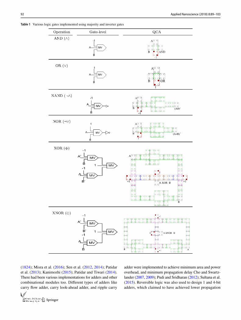
From literature we know that while a simple perceptron (a neuron without hidden layers) conveniently classifies AND, NAND, OR, NOR, and NOT gates, it is not able to classify XOR and XNOR gates Yanling et al. (2002). To be able to build a generic structure, it is obvious to choose the solution that could classify all the gates with no exceptions—a multi-layer perceptron (MLP) (having one or more hidden layers), presented in Fig. 2. Apparently it seems to add an overhead to have used an MLP for the operators other than XOR and XNOR, but considering the fact that only one cell will replace seven, this overhead seems affordable. In the next section, we will describe design of the logic cell built on an MLP.
(2)yk = �
(
M∑
j=0
wy
kl�H
(
M∑
j=0
wHijPR
))
(3)� =1
2
M∑
k=1
(yk − dk) =1
2
M∑
k=1
e2k
Related work
Reconfigurable ALU implementations on CMOS
Reconfigurable computing turns out to be a revolutionary methodology for computational logic while forming new architectures by decreasing area, power and speed over-heads. Various architectures were proposed in this regard that were based on re-configurability using the FPGAs Laxmi et al. (2012), a few of which made use of ANN, but unfortunately could not yield much impressive results Rafid and Saad (2009). A ternary ALU (using three-state clock cycle) was introduced with faster computations Haidar et al. (2008). Another ANN-based reconfigurable ALU was designed for digital signal processing applications with functions of additions, subtraction, multiplication, division, power, denoising (sine) and denoising (Gausian) Basu et al. (2015). It compromised on area but improved power and throughput. The design of a 32-bit ALU was proposed that allowed low-power consumption. The technique resulted in 18% reduction in power dissipation for 180 nm bulk CMOS technology, with a slight degradation in performance. In addition, there was a reduction in standby leakage power of 22 and 23% lower peak current Chatterjee et al. (2005). A reversible ALU was also proposed in literature to reduce propagation delay by 1 ns as compared to the conventional 1-bit ALU Mahayadin et al. (2014).
ALU implementations on QCA
A QCA based 1-bit ALU was proposed with logic operation ∧ , ∨ , ¬ , and arithmetic functions of addition (
∑
) and subtrac-tion ( ¬
∑
) using QCA-Designer. The ALU measured 1.67 μm2 in area, and incurred a latency of 9 clock cycles Gupta et al. (2012). Similarly, several other ALU implementations were presented; a few of those targeted smaller area, while the oth-ers opted for reduced latency Gupta et al. (2013); Ganesh
Fig. 1 Elementary logic gates in QCA: a majority gate, b inverter 1, c inverter 2
92 Applied Nanoscience (2018) 8:89–103
1 3
(1824); Misra et al. (2016); Sen et al. (2012, 2014); Patidar et al. (2013); Kanimozhi (2015); Patidar and Tiwari (2014). There had been various implementations for adders and other combinational modules too. Different types of adders like carry flow adder, carry look-ahead adder, and ripple carry
adder were implemented to achieve minimum area and power overhead, and minimum propagation delay Cho and Swartz-lander (2007, 2009); Pudi and Sridharan (2012); Sultana et al. (2015). Reversible logic was also used to design 1 and 4-bit adders, which claimed to have achieved lower propagation
Table 1 Various logic gates implemented using majority and inverter gates
93Applied Nanoscience (2018) 8:89–103
1 3
delay as compared to previous implementations by a half clock cycle Kunalan et al. (2014). That 1 bit adder cost an area of 0.67 μm2 and four clock cycles of latency. We believe, if a complete ALU was implemented using this reversible logic (with circuits for subtractor and other logic gates, etc.) it would have resulted in a substantially increased area and power overhead, beside yielding greater latency as compared to other ALUs.
In Sect. 4, we will present a comparison of the available ALUs for QCA. Generally, it is difficult to compare the avail-able works in terms of area utilization and latency, since either they are different sized, or do not have a provision for a few logic operations. For example, most of the designs summa-rized in Sect. 4, did not include a mux to choose one result amongst various arithmetic and logic operations. To get a fair comparison, all the ALUs are first required to be scaled; we have taken a liberty to complete the ALUs with all seven logic, two arithmetic operations, and a mux that chooses result of the desired operation ourselves. In Sect. 4, we will demonstrate that the mux we have designed and augmented with the exist-ing ALUs, is also more area efficient than a few existing ones.
In another work Beigh et al. (2013), the authors presented seven different implementations for an XOR gate, each with a different latency in terms of clock cycles, different complexity level, and a different number of cell count. The authors pointed out that the QCA-based designs were very much dependent on routing and cells placement.
Proposed methodology and system design
As mentioned already, the designers working with the QCA paradigm are required to manually perform the optimiza-tion of digital circuits, in terms of both area and latency. We
believe that ANN can play a vital role through the diversity in a perceptron, as discussed above, in circumventing this outstanding problem with QCA. For example, in case of an ALU, instead of having two separate blocks for logic and arithmetic computations, the dynamically reconfigurable ALU (DR-ALU), built on the proposed logic cell, will only require one block that may be reconfigured to perform the desired operation as needed. We expect that our proposed approach, besides resulting in a much smaller circuit, will make routing easy both in CMOS and QCA technologies.
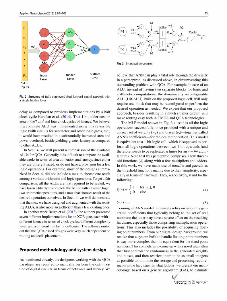
The MLP model shown in Fig. 3 classifies all the logic operations successfully, once provided with a unique and correct set of weights ( wij ) and biases ( bi)—together called ANN’s coefficients—for the desired operation. This model is equivalent to a 1-bit logic cell, which is supposed to per-form all logic operations between two 1-bit operands (and therefore, needs to be replicated n times for an n − bit archi-tecture). Note that this perceptron comprises a few thresh-old functions ( � ) along with a few multipliers and adders. In this work, we have made use of hardlim and purelin as the threshold functions mainly due to their simplicity, espe-cially in terms of hardware. They, respectively, stand for the following:
Training an ANN model immensely relies on randomly gen-erated coefficients that typically belong to the set of real numbers; the latter may have a severe effect on the resulting hardware, especially those comprising multiplication opera-tions. This also includes the possibility of acquiring float-ing point numbers. From our digital design background, we realize that a system built to handle floating point numbers is way more complex than its equivalent for the fixed point numbers. This compels us to come up with a novel algorithm that first controls the randomness in the generated weights and biases, and then restricts them to be as small integers as possible to minimize the storage and processing require-ments in the hardware. In what follows, we present our meth-odology, based on a genetic algorithm (GA), to estimate
(4)�i(n) =
{
1 for n ≥ 0
0 else
(5)�i(n) = n
Fig. 2 Structure of fully connected feed-forward neural network with a single hidden layer
P2
P1
b2
w11w21
w12w22
b3
Purelin
b1w31
w32
Hardlim
Hardlim
m1j
m2j f2
f1
m3j
Output
Fig. 3 Proposed perceptron
94 Applied Nanoscience (2018) 8:89–103
1 3
these parameters, followed by manual optimization of the perceptron suitable for binary logic, and QCA implementa-tion of the resulting Boolean expression.
GA framework
GAs are biologically inspired stochastic search algorithms, which guide a population of possible solutions toward an opti-mal solution based on the principle of survival of the fittest. In our proposed framework, set of weights and biases is repre-sented by a string called chromosome, which is replicated to generate a population of given size. For each iteration, fitness is calculated to achieve minimum mean squared error by fol-lowing fundamental GA operations which include crossover, mutation, and selection. A brief description of each operator used is given below.
Arithmetic crossover operator
Selecting a pair of chromosome C1i= (G1
1,G1
2,… ,G1
m) and
C2i = (G2
1 , G2
2,… ,G2
m) for an arithmetic crossover description.
An Offspring pair is generated, Ok = (gk1, gk
2,… , gk
m) , k = 1, 2
where: g1i= �G1
i+ (1 − �)G2
i and g2
i= �G2
i+ (1 − �)G1
i . �
is chosen to be a constant operator ( � = 0.5 ) but can vary with the number of generations as in non-uniform arithmetic crossover Jin et al. (2017).
Mutation operator
Under the same consideration as above, let Rmax be the maxi-mum number of generations and Rt be a generation on which mutation Ginley et al. (2011) is applied, then:
where �i and �i are selected to be 0 and 1 with a probability of 0.1.
Selection
Chromosome with smallest cost function value is selected where the selection rate ( �rate ) defines the number of sur-vivors need to mate in the next generation. Generally, �rate is selected to be 50% of the total population Razali et al. (2011).
(6)G�
i=
{
Gi + �(t, �i − Gi) if Gi = 0
Gi + �(t,Gi − �i) if Gi = 1
The selection probability depends on the cost weight, cal-culated as
Generation of weights and biases
Selection of the most optimum features in a finite solution space is very hard, especially with traditional binary-coded GA, which is prone to select N/2 number of features. Each chromosome from a population needs to fulfill the fitness criterion, which is the basis for the selection process. All chromosomes/individuals with better fitness value will have a better breeding chance compared to the individual with lower fitness value. In experimental results, it is sug-gested not to keep the selection criterion very harsh, so as to ensure the presence of individuals with lower fit-ness value which undoubtedly increases the population diversity.
Let Ψmpop
be the assembly of all generated chromosomes
having m feature components. The primary goal is to select the offsprings with highest fitness from solution space Ψ = ΨN
m=1Ψm . The randomly generated chromosome,
Gmi⊆ [−Rmin ≤ Ck ≤ Rmax] , where R� is the chromosome’s
range in integers, between − 3 and 3. Population is gener-ated based on Gaussian distribution, within the given range.
Considering all above parameters, we come up with a hybrid solution, Algorithm 1, which consolidates two different domains to generate a chromosome with best fitness value, which should have a minimal effect on the resulting hard-ware. It has two primary units; (1) generation of GA opti-mized coefficients; (2) ANN trained model which utilizes optimal combination of weights and biases generated in step 1 to perform seven logic operations.
(7)�rem = �rate × �pop
(8)�keep = �pop − �rem
(9)Pk =Ck
∑�keep
j=1Cj
(10)�mk= round(range(ℕ(m;�k, �
2) ∈ Gmi;ℝ2))

95Applied Nanoscience (2018) 8:89–103
1 3
Algorithm 1:Result: Trained ANN model with GA optimized coefficients
1 Begin:2 Initialize step size (δS), learning rate (δr), k, ε and weights and biases vector δWB .3 t ← 04 pop0 ← Initialize a population (popsize) from δWB
5 Evaluate pop06 while t < Genmax do7 Parents (χpar) ← Select χpar from popt8 Offspring (χofs) ← crossover (χofs, Cprob)9 mutation (χofs, Mprob)
10 Evaluate χofs
11 popt+1 ← actual population through replacement12 popt & χ′
ofs
13 t = t+ 114 end15 Return (Optimized weights and biases vector χ′
ofs)16 t′ ← 017 while t′ < (Maxepochs || ε) do18 Perform training using selected training algorithm to compute predicted value
φ̃pred
19 Update ∆W & ∆B20 Calculate difference betwee actual and predicted output21 if (φ̃pred ≤ ε) then22 Exit23 end24 end25 Return (Trained network)
Table 2 shows all the weights and biases generated by our algorithm for each of the logic operation. It may be conveni-ently verified that these values, once applied on the MLP, correctly classify the corresponding logic operation.
Manual optimization
Let each threshold function, �(X) , in Fig. 3 represent a neuron Nh
k : then the input to each neuron i in the hid-
den layer will be one of mij = bi + wi1P1 + wi2P2 , where j ∈ {1 → 4} for four possible binary combinations of two 1-bit operands Θ{0,1} . The description of hardlim sug-gests that output �i for each neuron in the hidden layer
will be low for negative numbers, and high otherwise, which requires the circuit to simply check the sign bit—usually the left-most bit in the bit-vector, also termed as the most significant bit (MSB). Therefore, the input to each neuron in the hidden layer may now be simplified to mij = MSB(bi + wi1P1 + wi2P2) , which is either logic-1 or logic-0 depending upon the applied inputs—enabling us to completely get rid of the costly multiplier and adder, and replace them with a much simpler mux. Similarly, input to the neuron Nout
i in the output layer of the given perceptron
will be m3j = MSB(b3 + w31f1 + w32f2).Extending the reconfigurable logic cell to incorporate
the arithmetic unit merely requires extension in number of
Table 2 ANN generated weights and biases for the MLP
No. Logic operation
Weights Biases
w11 w12 w21 w22 w31 w32 b1 b2 b3
1 ∧ − 3 0 1 − 1 − 1 − 1 0 − 1 12 ∨ 1 0 − 1 1 1 1 − 1 − 1 03 ¬∧ − 1 − 1 0 0 1 1 1 − 1 04 ¬∨ − 2 − 2 0 − 1 1 1 − 1 1 05 ¬ − 1 − 1 0 0 1 1 1 − 1 06 ⊕ − 3 1 1 − 1 1 1 − 1 − 1 07 ⊙ − 3 1 1 − 1 − 1 − 1 − 1 − 1 1
96 Applied Nanoscience (2018) 8:89–103
1 3
inputs of the mux; i.e., in addition to the logic operations, neuron-1 and neuron-2 will now compute {sum (S), dif-ference (D)} and {carry (C), borrow (B)} respectively as well. This resorts to the following set of equations for a full adder (that generates S and C) and a full subtractor (that generates D and B): S = A�B�C + AB�C + ABC� + ABC , C = A�BC + ABC + AB , D = A�B�C + AB�C + ABC� + ABC , and B = AB�C + ABC + A�B , where A and B represent the two 1-bit operands, and C is exclusively needed by the arithmetic operations. Following the manual optimiza-tion of the equations, f1 , f2 , and Output give the expected Boolean expressions for neuron-1, neuron-2, and neuron-3 respectively, which we need to implement on QCA.
Table 3 summarizes the optimized input to each neuron as per the desired arithmetic or logic operation. The table should be interpreted as follows: for the two operands 00, if the desired operation is AND, the inputs to neuron-1 ( m11 ), neuron-2 ( m21 ), and neuron-3 ( m31 ) should be 0, 1, and 0 respectively, and so on.
(11)f1 = ¬P1(¬P2 m11 + P2 m12) + P1(¬P2 m13 + P2 m14)
(12)f2 = ¬P1(¬P2 m21 + P2 m22) + P1(¬P2 m23 + P2 m24)
(13)Output = f1(f2 m31 + ¬f2 m32) + ¬f1(f2 m33 + f2 m34)
Table 3 Optimized entries for neuron-1, neuron-2, and neuron-3
Θ{0,1} mij ∧ ∨ ¬∧ ¬∨ ¬ ⊕ ⊙ S/C D/B
00 m11 0 1 0 0 0 1 1 C C01 m12 0 1 0 1 – 0 0 ¬C ¬C10 m13 1 0 0 1 – 1 1 ¬C ¬C11 m14 1 0 1 1 1 1 1 C C00 m21 1 1 1 1 1 1 1 0 C01 m22 1 0 1 1 – 1 1 C 110 m23 0 1 1 1 – 0 0 C 011 m24 1 1 1 1 1 1 1 1 C00 m31 0 1 0 0 0 0 1 – –01 m32 0 1 1 1 1 1 0 – –10 m33 0 1 0 0 0 1 0 – –11 m34 1 0 0 0 0 0 1 – –
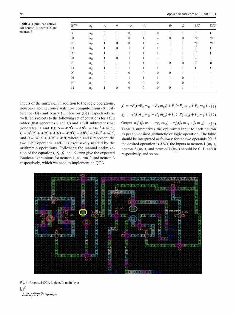
Fig. 4 Proposed QCA logic cell: main layer
97Applied Nanoscience (2018) 8:89–103
1 3
QCA implementation
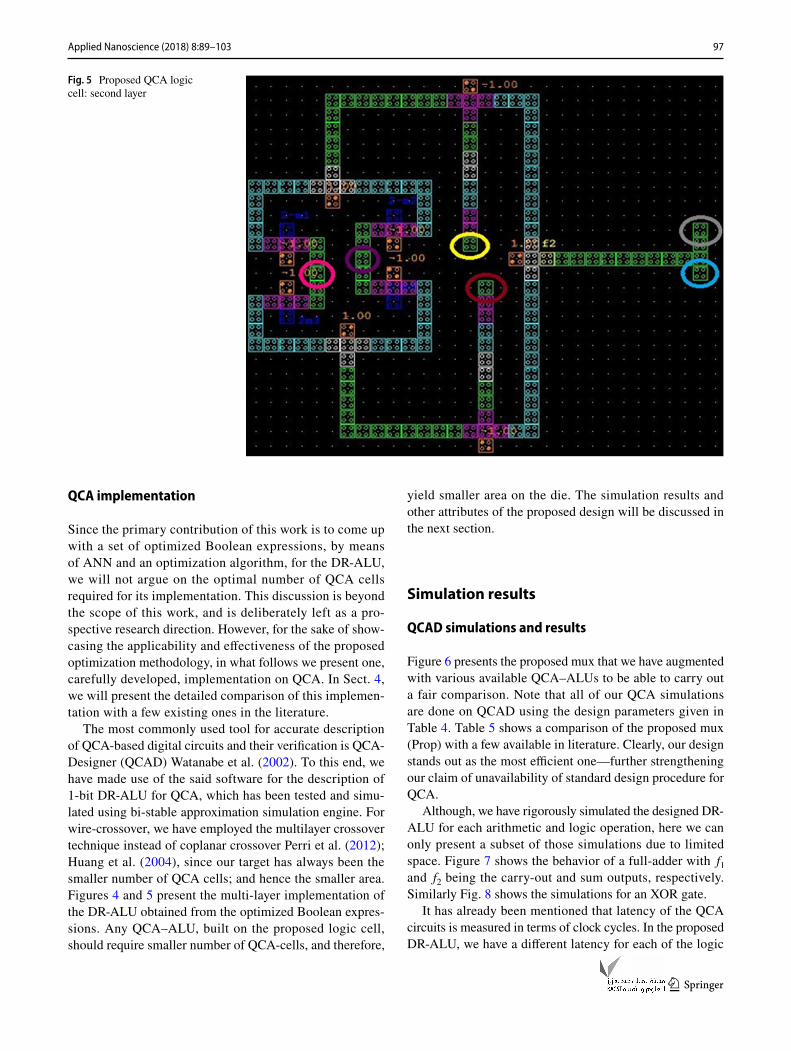
Since the primary contribution of this work is to come up with a set of optimized Boolean expressions, by means of ANN and an optimization algorithm, for the DR-ALU, we will not argue on the optimal number of QCA cells required for its implementation. This discussion is beyond the scope of this work, and is deliberately left as a pro-spective research direction. However, for the sake of show-casing the applicability and effectiveness of the proposed optimization methodology, in what follows we present one, carefully developed, implementation on QCA. In Sect. 4, we will present the detailed comparison of this implemen-tation with a few existing ones in the literature.
The most commonly used tool for accurate description of QCA-based digital circuits and their verification is QCA-Designer (QCAD) Watanabe et al. (2002). To this end, we have made use of the said software for the description of 1-bit DR-ALU for QCA, which has been tested and simu-lated using bi-stable approximation simulation engine. For wire-crossover, we have employed the multilayer crossover technique instead of coplanar crossover Perri et al. (2012); Huang et al. (2004), since our target has always been the smaller number of QCA cells; and hence the smaller area. Figures 4 and 5 present the multi-layer implementation of the DR-ALU obtained from the optimized Boolean expres-sions. Any QCA–ALU, built on the proposed logic cell, should require smaller number of QCA-cells, and therefore,
yield smaller area on the die. The simulation results and other attributes of the proposed design will be discussed in the next section.
Simulation results
QCAD simulations and results
Figure 6 presents the proposed mux that we have augmented with various available QCA–ALUs to be able to carry out a fair comparison. Note that all of our QCA simulations are done on QCAD using the design parameters given in Table 4. Table 5 shows a comparison of the proposed mux (Prop) with a few available in literature. Clearly, our design stands out as the most efficient one—further strengthening our claim of unavailability of standard design procedure for QCA.
Although, we have rigorously simulated the designed DR-ALU for each arithmetic and logic operation, here we can only present a subset of those simulations due to limited space. Figure 7 shows the behavior of a full-adder with f1 and f2 being the carry-out and sum outputs, respectively. Similarly Fig. 8 shows the simulations for an XOR gate.
It has already been mentioned that latency of the QCA circuits is measured in terms of clock cycles. In the proposed DR-ALU, we have a different latency for each of the logic
Fig. 5 Proposed QCA logic cell: second layer

98 Applied Nanoscience (2018) 8:89–103
1 3
and the arithmetic units, since the latter does not use the output layer neuron. While latency for the logic unit is four clock cycles, for the arithmetic unit it is estimated to be two. Most of the previously proposed QCA–ALUs, despite not
offering the complete functionality, have a latency greater than the proposed one. Table 6 summarizes the relevant benchmark works (ref.), their architectures (arch.), along with the functionality they offer and the results they achieve in terms of cell-count, latency, and area utilization. The table also lists the same for the proposed work (Prop).
Clearly, the works Ganesh (1824) and Sen et al. (2014) are the closest to the proposed, except for the fact that they both lack two functions, and the former does not have the mux for choosing the final result in addition. The enormous difference in the area utilization between those works and the proposed is mainly due to the multi-layer wire-crossing
Fig. 6 Proposed multiplexer
−1
−1
1− 1−
−1
−1
1
11
Out
I1
I2
I3
I4
S2
S1
Table 4 Design parameters for QCAD simulations
Parameter Value
Method Bistable approximation engine
QCA cell width 18 nmQCA cell height 18 nmDot diameter 5 nmRelative permittivity 12.9 nmRadius of effect 65.00 nmClock high 9.800000e− 022Clock low 3.800000e−023Clock shift 0.000000e+000Clock amplitude factor 2No. of samples 12800layer separation 11.5Convergence tolerance 0.001Maximum iterations per sample 100
Table 5 Comparison of 4-input mux
Reference Cell count Area Latency(μm2) (cycles)
Ramesh and Asha (2014) 409 .76 2.5Mukhopadhyay et al. (2011) 166 .25 1Mardiris et al. (2010) 215 .25 6Sen et al. (2015) 155 .24 5Sabbaghi-Nadooshan et al. (2014) 271 .37 19Prop 142 .16 1.5

99Applied Nanoscience (2018) 8:89–103
1 3
technique we have employed: it is complicated, but more area efficient.
Note that for a fair comparison, we have augmented our own mux, Fig. 6, with those ALUs not having it already, and redesigned each of them to have all the logic and arith-metic operations as the proposed one. Now the comparison, in terms of area utilization, is given in Fig. 9. It is evident
that for an identical set of operations, the proposed work is significantly smaller than the benchmark works.
FPGA implementation and synthesis
As the last exercise, what remained to be evaluated was that our ANN and GA based optimization had not altered the original functionality of the ALU. We implemented
Fig. 7 QCAD simulation of the full adder

100 Applied Nanoscience (2018) 8:89–103
1 3
the optimized Boolean expressions on an FPGA from Xilinx, performed equivalence checking, and ran several simulations for each logic and arithmetic operation. Fig-ures 10 and 11 present two sample simulations: while the former corresponds to arithmetic unit, the latter presents
simulations for each logic operation. Besides being func-tionally correct, our FPGA synthesis yielded 40% reduc-tion in area as compared to a CMOS–ALU designed by a usual behavioral description.
Fig. 8 QCAD simulation of the XOR gate

101Applied Nanoscience (2018) 8:89–103
1 3
Conclusion
The state-of-the-art in quantum-dot cellular automata (QCA) lacks in a standard implementation methodol-ogy for digital circuits in general, and an arithmetic and logic unit (ALU) in particular. This quagmire has led to several vastly different implementations for ALU—each advocating its merits, usually in terms of cell-count, area utilization, and latency. In this work, we have attempted to address this issue by proposing an optimized set of Boolean expressions, which we have called a dynami-cally reconfigurable (DR) logic cell. The cell is capable of reconfiguring itself to perform various arithmetic and logic operations—one at a time—as needed. While the reconfigurability of the cell is achieved by providing a unique set of weights and biases, called coefficients, to a trained artificial neural networks based model, the
Table 6 Comparison of the existing QCA–ALUs with the proposed one
Ref. Arch. Operations Mux? Cell Area LatencyCount (μm2) (cycles)
Gupta et al. (2012) 1-bit∑
,·
,∧,∨,¬ ✓ – 1.67 9Gupta et al. (2013) 2-bit
∑
,·
,∧,∨,¬ ✓ – 3.4 9Ganesh (1824) 1-bit
∑
,·
,∧,∨,¬,¬∧,¬∨ ✗ 494 0.92 1Misra et al. (2016) 1-bit
∑
,∧,∨,¬,¬∧,¬∨ ✗ 233 0.29 2.5Sen et al. (2012) 1-bit
∑
,∧,∨,¬,¬∧,¬∨ ✗ 194 0.21 1.25Sen et al. (2014) 1-bit
∑
,·
,∧,∨,¬,¬∧,¬∨ ✓ – 4.06 6Patidar et al. (2013) 4 bit
∑
,·
,∧,∨,¬ ✓ 4738 7.64 15Pandimeena et al. (2017) 1 bit
∑
,∧,∨,¬,⊕ ✗ 201 6.51 –Prop 1-bit
∑
,·
,∧,∨,¬∧,¬∨,¬,⊕,⊙ ✓ 587 0.58 4
Fig. 9 Comparison of area of the proposed DR-ALU with the exist-ing designs: a Gupta et al. (2012), b Gupta et al. (2013), c Ganesh (1824), d Misra et al. (2016), e Sen et al. (2012), f Sen et al. (2014), g Patidar et al. (2013), h Patidar and Tiwari (2014), i Pandimeena et al. (2017), j Prop
Fig. 10 FPGA simulation of the arithmetic unit
Fig. 11 FPGA simulation of the logic unit
102 Applied Nanoscience (2018) 8:89–103
1 3
coefficients themselves have been optimized by means of a genetic algorithm. The optimization technique is meant to control the randomness in the generation of coefficients, so as to obtain only fixed point small integers, which should have a minimal effect on the resulting hardware. We have demonstrated how this cell may be replicated and appo-sitely organized to build a complete DR-ALU, which is much smaller than the existing equivalents. In addition to this, we have proposed a novel multiplexer, which is also more area efficient as compared to several existing works.
Autonomously determining the minimal number of QCA cells to implement a given Boolean expression still remains an outstanding research problem. This we have left as a pro-spective research direction that we intend to address in near future.
References
Anderson NG, Bhanja S (eds) (2014) Field-coupled nanocomputing: paradigms, progress, and perspectives, vol 8280. Springer, Berlin
Basu M, Pandey A, Mustafi A (2015) An Analytical Neural Network for Arithmetic Logic Unit of Microprocessors. In: Conference National Symposium on Recent Trends in Instrumentation Sci-ence and Technology, Kolkata, pp 1–4
Beigh MR, Mustafa M, Ahmad F (2013) Performance evaluation of efficient XOR structures in quantum-dot cellular automata (QCA). Circuits Syst 4(02):147
Berggren K-F, Yakymenki I (2006) Quantum cellular automata - Theory, experimentation and prospects. Imperial College Press, London, 300p
Chatterjee B, Sachdev M (2005) Design of a 1.7-GHz low-power delay-fault-testable 32-b ALU in 180-nm CMOS technology. IEEE Trans Very Large Scale Integr (VLSI) Syst 13(11):1296–1304
Cho H, Swartzlander EE Jr (2007) Adder design and analyses forquan-tum-dot cellular automata. IEEE Trans Nanotechnol 6(3):374383
Cho H, Swartzlander EE Jr (2009) Adder and multiplier design in quantum-dot cellular automata. IEEE Trans Comput 58(6):721727
Ganesh EN (1824) Implementation and simulation of arithmetic logic unit, shifter and multiplier in quantum cellular automata technol-ogy. Int J Comput Sci Eng 2(5):2010
Güçlü U, van Gerven MAJ (2015) Deep neural networks reveal a gradi-ent in the complexity of neural representations across the ventral stream. J Neurosci 35(27):10005–10014
Gupta N, Shrivastava S, Patidar N, Katiyal S, Choudhary KK (2012) Design of one bit arithmetic logic unit (ALU) in QCA. Int J Com-put Appl Eng Sci 2(3):281–285
Gupta N, Choudhary KK, Katiyal S (2013) Two Bit Arithmetic Logic Unit (ALU) in QCA. Int J Recent Trends. Eng Technol 8(2):35
Haidar A et al (2008) A novel neural network ternary arithmetic logic unit. Complement 2:1
Haider SA, Naqvi SR, Akram T et al (2017) Modeling electrical prop-erties for various geometries of antidots on a superconducting film. Appl Nanosci 7(8):933–945
Haider SA et al (2017) Prediction of critical currents for a diluted square lattice using artificial neural networks. Appl Sci 7(3):238
Haykin SS et al (2009) Neural networks and learning machines, vol 3. Pearson, Upper Saddle River
Huang, J, Momenzadeh M, Tahoori MB, Lombardi F (2004) Defect characterization for scaling of QCA devices [quantum dot cellular automata]. In: Defect and fault tolerance in VLSI systems, 2004.
DFT 2004. Proceedings. 19th IEEE international symposium on, pp 30–38, IEEE
Jayalakshmi R, Amutha R (2016) Quantum dot Cellular Automata a review on the new paradigm in computation. In: Advances in electrical, electronics, information, communication and bio-infor-matics (AEEICB), 2016 2nd international conference on IEEE
Jin C et al (2017) A new compound arithmetic crossover-based genetic algorithm for constrained optimisation in enterprise systems. Enterp Inf Syst 11(1):122–136
Kalogeiton VS et al (2017) Programmable crossbar quantum-dot cel-lular automata circuits. IEEE Trans Comput Aided Des Integr Circuits Syst 36(8):1367–1380
Kamran M et al (2016) Prediction of IV curves for a superconducting thin film using artificial neural networks. Superlattices Micro-struct 95:88–94
Kanimozhi V (2015) Design and implementation of Arithmetic Logic Unit (ALU) using modified novel bit adder in QCA. In: Inno-vations in information, embedded and communication systems (ICIIECS), 2015 international conference on, pp 1–6, IEEE
Kunalan D, Cheong CL, Chau CF, Ghazali AB (2014) Design of a 4-bit adder using reversible logic in quantum-dot cellular automata (QCA). In: Semiconductor electronics (ICSE), 2014 IEEE inter-national conference on, pp 60–63, IEEE
Laxmi V, Adiga CS, Harish SV (2012) FPGA Based Reconfigurable Computing Systems: a New Design Approach - a Review. Adv Mater Res 403(408):4272–4278
Lombardi F, Huang J (2007) Design and test of digital circuits by quan-tum-dot cellular automata. Artech House Inc., Norwood
Mahayadin NSM et al (2014) Design and synthesis of reversible arith-metic and Logic Unit (ALU). In: IEEE Intn Conf on: Computer, Communications, and Control Technology (ICT), pp 289–293
Mardiris VA, Karafyllidis IG (2010) Design and simulation of modular 2n to 1 quantumdot cellular automata (QCA) multiplexers. Int J Circuit Theory Appl 38(8):771–785
Mc Ginley B et al (2011) Maintaining healthy population diversity using adaptive crossover, mutation, and selection. IEEE Trans Evol Comput 15(5):692–714
Misra NK, Wairya S, Singh VK (2016) Approach to design a high performance fault-tolerant reversible ALU. Int J Circuits Archit Des 2(1):83–103
Momenzadeh M et al (2005) Characterization, test, and logic syn-thesis of and-or-inverter (AOI) gate design for QCA imple-mentation. IEEE Trans Comput Aided Des Integr Circuits Syst 24(12):1881–1893
Mukhopadhyay D, Dinda S, Dutta P (2011) Designing and implemen-tation of quantum cellular automata 2: 1 multiplexer circuit. Int J Comput Appl 25(1):21–24
Naqvi SR, Akram T, Haider SA et al (2016) Artificial neural networks based dynamic priority arbitration for asynchronous flow con-trol. Neural Comput Appl 1–11. https ://doi.org/10.1007/s0052 1-016-2571-6
Niemier M, Kogge P (2001) Problems in designing with QCAs: layout equals timing. Int J Circuit Theory Appl 29:49–62
Pandimeena R, Nirmala J, Shanmugapriya M, Tamilselvi M (2017) Area-delay efficient arithmetic logic unit using qca. In: SSRG international journal of electronics and communication engineer-ing—(Icrtecita-2017), Special Issue, March 2017
Patidar N, Gupta N, Kha bia A, Katiyal S, Choudhary KK (2013) A novel 4-bit arithmetic logic unit implementation in quantum-dot cellular automata. Int J Nanotechnol Appl (IJNA) 1(3):1–8
Patidar S, Tiwari M (2014) An efficient design Of 1 bit arithmetic logic unit in quantum dot cellular automata. Int J Eng Sci Manag 1(1):1–8
Perri S, Pasquale C (2012) New methodology for the design of effi-cient binary addition circuits in QCA. IEEE Trans Nanotechnol 11(6):1192–1200

103Applied Nanoscience (2018) 8:89–103
1 3
Pudi V, Sridharan K (2012) Low complexity design of ripple Carry and Brent-kung adders in QCA. IEEE Trans Nanotechnol 11(1):105119
Rafid AK, Saad AA (2009) Digital hardware implementation of artifi-cial neurons models using FPGA. Al-Rafidain Eng 17(3):12–24
Ramesh B, Asha Rani M (2014) Implementation of quantum dot cel-lular automata based multiplexer on FPGA. Prog Sci Engg Res Jour 2(14):1–5
Razali NM, Geraghty J (2011) Genetic algorithm performance with dif-ferent selection strategies in solving TSP. In: Proceedings World congress on engineering Hong Kong: V. 2, pp 1134–1139
Sabbaghi-Nadooshan R, Kianpour M (2014) A novel QCA implemen-tation of MUX-based universal shift register. J Comput Electron 13(1):198–210
Sen B, Dutta M, Banik D, Singh DK, Sikdar BK (2012) Design of fault tolerant reversible arithmetic logic unit in QCA. In: Elec-tronic system design (ISED), 2012 international symposium on, pp 241–245, IEEE
Sen B, Dutta M, Goswami M, Sikdar BK (2014) Modular design of testable reversible ALU by QCA multiplexer with increase in pro-grammability. Microelectron J 45(11):1522–1532
Sen B et al (2015) Towards modular design of reliable quantum-dot cellular automata logic circuit using multiplexers. Comput Electr Eng 45:42–54
Singh S, Shraddha P, Subodh W (2016) Modular design of $2^{n}$: 1 quantum dot cellular automata multiplexers and its application,
via clock zone based crossover. Int J Modern Educ Comput Sci 8(7):41
Sultana T, Bardhan R, Bithee TF, Tabassum Z, Lisa NJ (2015) A compact design of n-bit ripple carry adder circuit using QCA architecture. In: Computer and information science (ICIS), 2015 IEEE/ACIS 14th international conference on, pp 155–160, IEEE
Tehrani MA, Safura B, Keivan N (2014) A novel ternary quantum-dot cell for solving majority voter gate problem. Appl Nanosci 4(3):255–262
Watanabe H, Suzuki M, Yamazaki J (2002) Qcad: gui environment for quantum computer simulator. http://apoll on.cc.u-tokyo .ac.jp/watan abe/qcad/(jun.2010) (2002)
Yamahata G et al. (2008) Enhanced tunnel conductance due to QCA cotunneling processes observed for silicon serial triple quantum dots. In: Solid-state device research conference, 2008. ESSDERC 2008. 38th European, IEEE
Yanling Z, Bimin D, Zhanrong W (2002) Analysis and study of percep-tron to solve XOR problem. In: Autonomous decentralized system, 2002. The 2nd international workshop on IEEE
Publisher’s Note Springer Nature remains neutral with regard to jurisdictional claims in published maps and institutional affiliations.