Embed Size (px)
Citation preview
White Paper
Advances in Light Curing Adhesives and Coatings Lead to Process and Quality Benefits in Electronics Manufacturing By Peter Swanson, MA (Cantab), Managing Director, INTERTRONICS Abstract
Radiation curing of adhesives and coatings continues to make technology advances. In particular, curing with light has seen many developments. Ultra violet curing technology has been enhanced by and is now allied with visible light curing. Visible light curing offers process improvements and advantages in health and safety. Synergistic use of UV and visible light gives better cure speeds and depths, and allows more applications, which were previously difficult or impossible. Light curing adhesives, coatings and encapsulants are being used in the electronics manufacturing industry with increasing frequency because their properties and process advantages are a good fit for the manufacturing requirements which are dictated by current industry drivers, such as miniaturisation, environmental and health & safety demands, manufacturing yield improvement and total product cost. Introduction
A recent paper by this author concentrated on current case histories of radiation cure (photo cure)
adhesives in this electronics manufacturing sector1. This paper will concentrate on the recent
developments which will shortly impact on or are recently introduced to the factory floor. Also, it
will muse upon some future possibilities for the technology.
Industry Drivers
The increasing take up of photo cure adhesives by the electronics manufacturing industry may in
part be explained by the general driving forces which prevail within it:
Miniaturisation - electronic products are getting smaller and faster.
Environmental demands - restrictions on volatile organic compounds which contribute
towards the greenhouse effect and the discussions about lead replacement are instances of
current issues. Companies have espoused the "green" ideal as an ethic.
Health & safety - increased responsibilities on companies for the safety of both their work
force, and also their customers, in the widest sense of that word.
Manufacturing yield improvement - high yields are achieved in electronics manufacture (6
sigma plus). The drive is to ensure that this level is routine. New technologies demand this
because, for example, inspection and rework processes can become expensive or
impossible.
Total product cost - to achieve cost improvements, it is important to examine the entire
process or product. A new element which is in itself more expensive may have process or
performance implications which reduce the total product cost.
Materials - the emphasis may be swinging from reliability to process-ability. This is not to
imply that reliability is not important, or even not paramount. But the need to fit materials
into a modern production environment with JIT philosophies means that their processing
must be simple and consistent.
Design for manufacture - in the quest for high functionality, performance and appealing
appearance, do not forget that someone has to produce it.
A Fundamental Change
In addition to these drivers, electronics manufacturing is undergoing a fundamental shift; it is
changing from assembly to process2. The assembly line introduced at Ford Motor Company in
October 1913 reduced the time required to assemble an automobile from 12.5 hours to 1.5 hours,
and revolutionised industry. We can still compare in our minds an electronics manufacturing factory
with a car assembly line, with the addition of components and parts as the product trundles along
some form of conveyor. But with increasing automation, and higher component functionality and
more complex integration, the emphasis must be changing towards process, from assembly. A
process line, where a series of operations are performed on the product, is the new paradigm.
Attention is focused on these processes, then, with the objective of minimising defects, down time,
work in progress and response time.
Light or Photo Curing
The Electromagnetic Spectrum
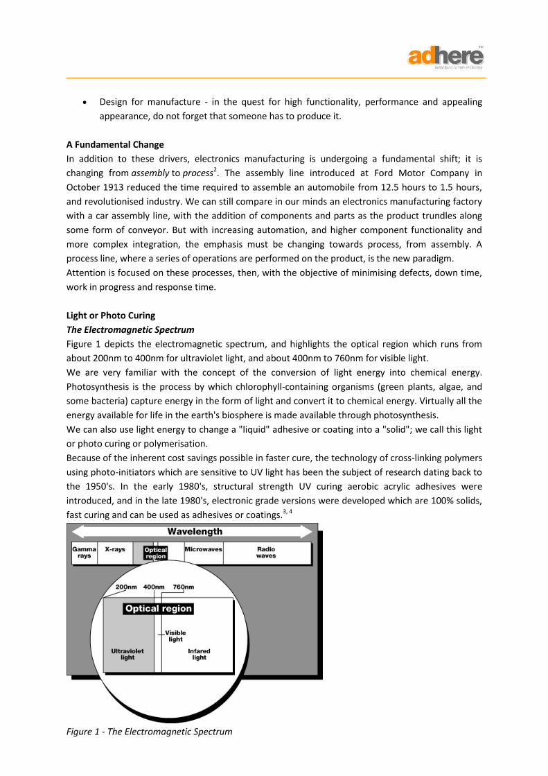
Figure 1 depicts the electromagnetic spectrum, and highlights the optical region which runs from
about 200nm to 400nm for ultraviolet light, and about 400nm to 760nm for visible light.
We are very familiar with the concept of the conversion of light energy into chemical energy.
Photosynthesis is the process by which chlorophyll-containing organisms (green plants, algae, and
some bacteria) capture energy in the form of light and convert it to chemical energy. Virtually all the
energy available for life in the earth's biosphere is made available through photosynthesis.
We can also use light energy to change a "liquid" adhesive or coating into a "solid"; we call this light
or photo curing or polymerisation.
Because of the inherent cost savings possible in faster cure, the technology of cross-linking polymers
using photo-initiators which are sensitive to UV light has been the subject of research dating back to
the 1950's. In the early 1980's, structural strength UV curing aerobic acrylic adhesives were
introduced, and in the late 1980's, electronic grade versions were developed which are 100% solids,
fast curing and can be used as adhesives or coatings.3, 4
Figure 1 - The Electromagnetic Spectrum
UV Cured Adhesives and Coatings
For electronics applications, the systems are primarily based on acrylic and urethane chemistries
(although light curing epoxies and silicones are known).
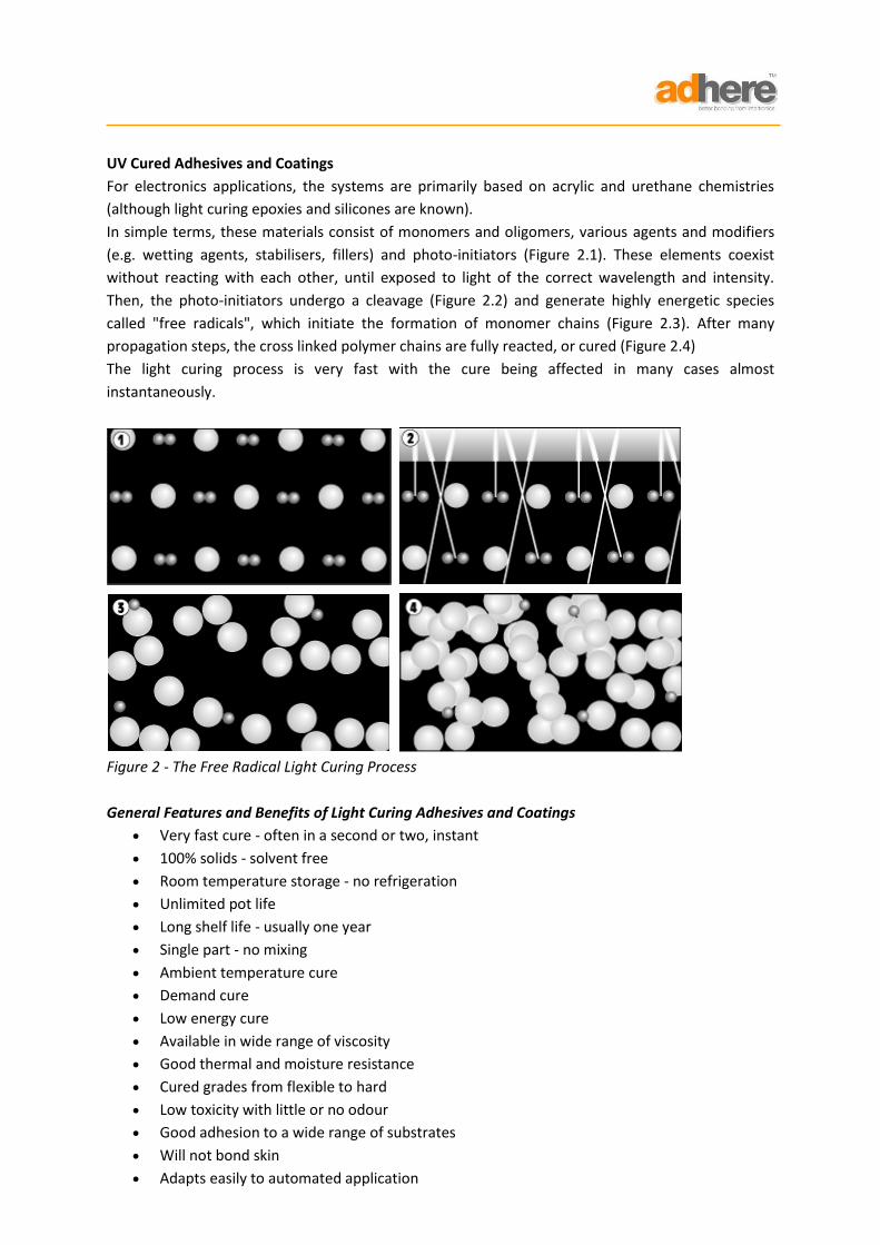
In simple terms, these materials consist of monomers and oligomers, various agents and modifiers
(e.g. wetting agents, stabilisers, fillers) and photo-initiators (Figure 2.1). These elements coexist
without reacting with each other, until exposed to light of the correct wavelength and intensity.
Then, the photo-initiators undergo a cleavage (Figure 2.2) and generate highly energetic species
called "free radicals", which initiate the formation of monomer chains (Figure 2.3). After many
propagation steps, the cross linked polymer chains are fully reacted, or cured (Figure 2.4)
The light curing process is very fast with the cure being affected in many cases almost
instantaneously.
Figure 2 - The Free Radical Light Curing Process
General Features and Benefits of Light Curing Adhesives and Coatings
Very fast cure - often in a second or two, instant
100% solids - solvent free
Room temperature storage - no refrigeration
Unlimited pot life
Long shelf life - usually one year
Single part - no mixing
Ambient temperature cure
Demand cure
Low energy cure
Available in wide range of viscosity
Good thermal and moisture resistance
Cured grades from flexible to hard
Low toxicity with little or no odour
Good adhesion to a wide range of substrates
Will not bond skin
Adapts easily to automated application
Electronics Applications
Since the late 80's, hundreds of successful applications have been found for this technology. Use has
been found in the electronics manufacturing industry in the following areas:
Strain relief
Wire and parts tacking
Coil terminating
Tamper-proofing
Structural bonding
Temporary masking
Potting
Encapsulation, glob topping, underfill
Conformal coating
Surface mount component attachment
Examination of a few case histories will demonstrate both the efficacy and the economics of using
light curing adhesives and coatings5.
UV Light Curing
Until recently, most light curing adhesives used in industry have been cured with ultra violet light.
Historically, the first UV inks and coatings were "dried" with shortwave UV light in the 250nm range.
These short wavelengths (UV-C) are hazardous; indeed, shortwave UV radiation can be used for
sterilisation. Applications are restricted to well-shielded conveyorised systems.
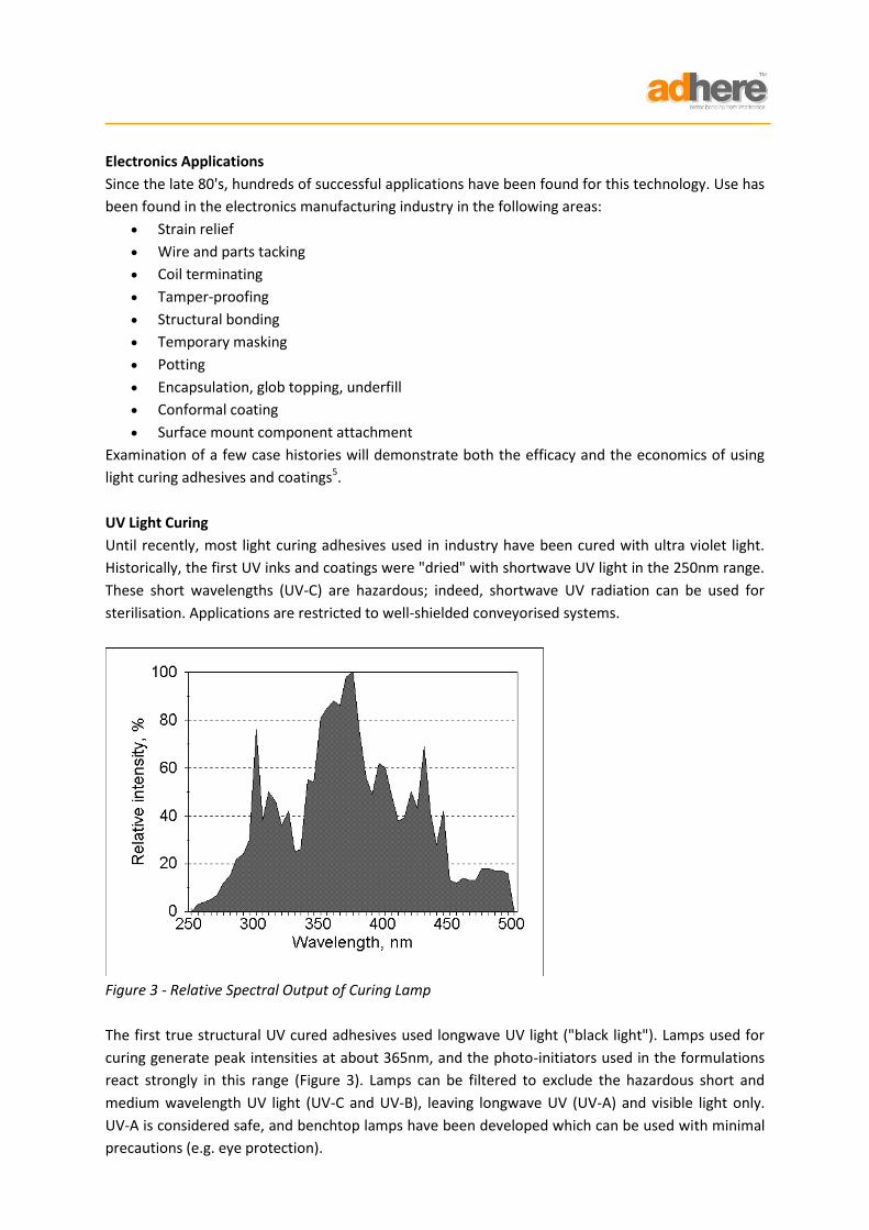
Figure 3 - Relative Spectral Output of Curing Lamp
The first true structural UV cured adhesives used longwave UV light ("black light"). Lamps used for
curing generate peak intensities at about 365nm, and the photo-initiators used in the formulations
react strongly in this range (Figure 3). Lamps can be filtered to exclude the hazardous short and
medium wavelength UV light (UV-C and UV-B), leaving longwave UV (UV-A) and visible light only.
UV-A is considered safe, and benchtop lamps have been developed which can be used with minimal
precautions (e.g. eye protection).
Cure Depth & Technology Restrictions
Light absorption by any material varies with wavelength. Short wavelength UV will be absorbed at
the very surface of the material, and thus is restricted to UV "drying" very thin layers (inks and
coatings). Because it is absorbed less well, longwave UV penetrates further. The first UV cure aerobic
acrylic adhesives used longwave UV to cure, and were thus able to succeed in applications such as
structural bonding, sealing and coating where cure depths could achieve up to 6-8mm.
Certain plastics do not transmit UV light very well, if at all. Some have UV blocking agents which are
added to prevent UV light ageing. Light curing technology would not work with many translucent,
coloured or UV blocked substrates. Adhesive applications were restricted to shallow potting, sealing,
bridge bonding or tacking applications where the adhesive is directly exposed to light. Potting and
encapsulation was limited to transparent resins or thin layers of pigmented resins.
Visible Light Curing
New formulations have added a visible light cure in addition to the ultra violet, extending the light
range usable by the adhesive up to about the 500nm level. This has given the technology of curing
with light a number of very important advantages over traditional UV curing.
Cure Speed
Advocates of photo cure technology are already benefiting from cure speeds of seconds compared
to minutes or hours for heat cure resins or solvent evaporation systems. The synergistic use of both
longwave UV and visible photo-catalysts in adhesive formulations typically yields cure speeds up to
50% faster than formulations which cure only by absorbed UV light.
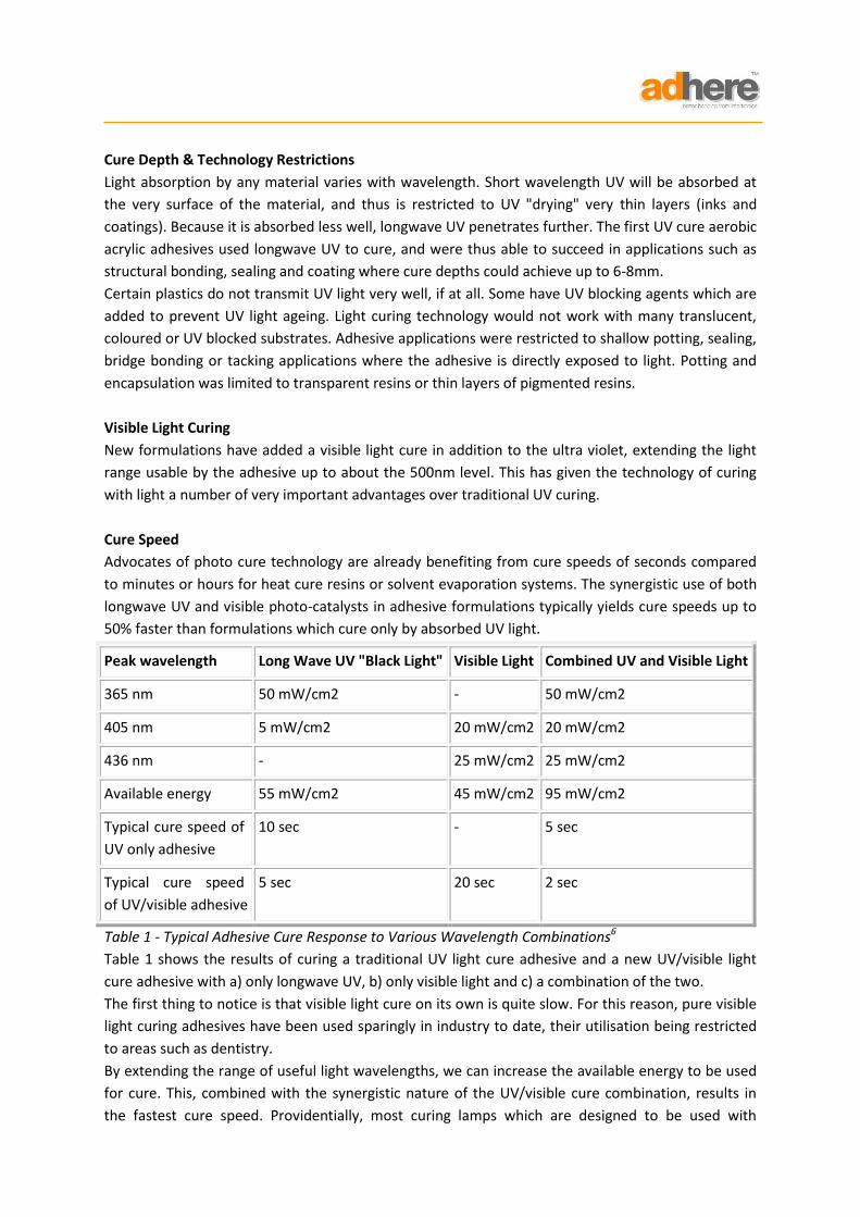
Peak wavelength Long Wave UV "Black Light" Visible Light Combined UV and Visible Light
365 nm 50 mW/cm2 - 50 mW/cm2
405 nm 5 mW/cm2 20 mW/cm2 20 mW/cm2
436 nm - 25 mW/cm2 25 mW/cm2
Available energy 55 mW/cm2 45 mW/cm2 95 mW/cm2
Typical cure speed of
UV only adhesive
10 sec - 5 sec
Typical cure speed
of UV/visible adhesive
5 sec 20 sec 2 sec
Table 1 - Typical Adhesive Cure Response to Various Wavelength Combinations6
Table 1 shows the results of curing a traditional UV light cure adhesive and a new UV/visible light
cure adhesive with a) only longwave UV, b) only visible light and c) a combination of the two.
The first thing to notice is that visible light cure on its own is quite slow. For this reason, pure visible
light curing adhesives have been used sparingly in industry to date, their utilisation being restricted
to areas such as dentistry.
By extending the range of useful light wavelengths, we can increase the available energy to be used
for cure. This, combined with the synergistic nature of the UV/visible cure combination, results in
the fastest cure speed. Providentially, most curing lamps which are designed to be used with
longwave UV curing adhesives emit appreciable visible light; users can take advantage of this new
technology without having to invest in new equipment.
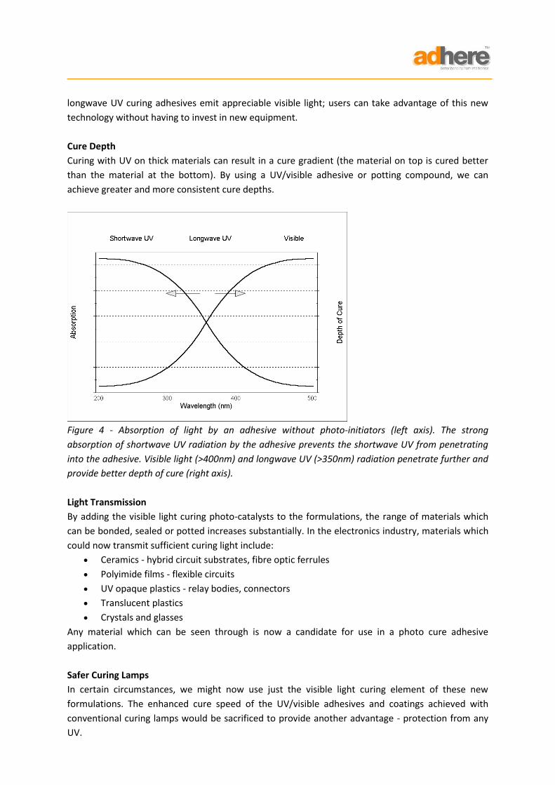
Cure Depth
Curing with UV on thick materials can result in a cure gradient (the material on top is cured better
than the material at the bottom). By using a UV/visible adhesive or potting compound, we can
achieve greater and more consistent cure depths.
Figure 4 - Absorption of light by an adhesive without photo-initiators (left axis). The strong
absorption of shortwave UV radiation by the adhesive prevents the shortwave UV from penetrating
into the adhesive. Visible light (>400nm) and longwave UV (>350nm) radiation penetrate further and
provide better depth of cure (right axis).
Light Transmission
By adding the visible light curing photo-catalysts to the formulations, the range of materials which
can be bonded, sealed or potted increases substantially. In the electronics industry, materials which
could now transmit sufficient curing light include:
Ceramics - hybrid circuit substrates, fibre optic ferrules
Polyimide films - flexible circuits
UV opaque plastics - relay bodies, connectors
Translucent plastics
Crystals and glasses
Any material which can be seen through is now a candidate for use in a photo cure adhesive
application.
Safer Curing Lamps
In certain circumstances, we might now use just the visible light curing element of these new
formulations. The enhanced cure speed of the UV/visible adhesives and coatings achieved with
conventional curing lamps would be sacrificed to provide another advantage - protection from any
UV.
Curing lamps are now available which output only intense "blue light", around the 420nm range.
These could be used when sensitive substrates are being bonded or coated, for example some
plastics which would quickly degrade under UV light, or circuitry which is optically delicate.
Occasionally, conventional UV curing lamps cannot be used safely, or are perceived to be unsafe, in
an application. This is despite the fact that, with appropriate safety wear (eye protection, gloves), it
has been shown that operators' exposure to UV radiation from bench top curing lamps is well within
safety limits and is harmless. Often these lamps are filtered to produce only safe, longwave UV-A.
However, in these instances, a low intensity "black light" inspection lamp or a high intensity visible
light lamp may be used for curing.
Filled Adhesives and Coating
With the additional penetration afforded by the use of a UV/visible light cure mechanism, adhesives
and coatings may be formulated to contain some filler and still achieve good cure speeds and depths
curing with light alone. Thickness of cured material will depend on bond geometry, intensity of light
used and transmission characteristics of the fillers. Examples of fillers are borosilicate glass or
alumina. Desirable enhanced properties of these filled adhesives or coatings are:
Very low shrinkage - for precision bonding
Thermal conductivity - heat sink attachment
Electrical conductivity
Opacity - security, cosmetics
Practical Considerations
Ambient light found in factories or outdoors in sunlight will eventually cure UV/visible light systems,
but the light intensity required to quickly cure UV/visible light systems is much higher. While
sensitive to light in the visible spectrum, the systems have very long open pot lives, and will stay in
their "liquid" state until exposed to intense light, and then cure very quickly. Thus, they retain the
very desirable "demand" cure property of UV cured systems. In the correct packaging which blocks
100% of both UV and visible light, the materials have very good packaging stability, usually in excess
of twelve months at ambient storage temperature.
Secondary Cure Mechanisms
Even with the improved speeds and depths of cure given by combined UV/visible systems, full cure
by light alone may not be possible in every application. Shadowing caused by component geometry
(or adhesive fillers) may not allow even penetrative visible light to reach all areas of the adhesive or
coating. Generally speaking, light curing adhesives and coatings will start cross-linking when the light
is shone upon them, and stop almost immediately when the light is taken away. There is little or no
proliferation of the cure into areas which are shielded from the light. As an aside, this phenomena
means improved product stability on the shelf.
When there are shadowed areas, a secondary cure mechanism can be employed to complete the
cure. Anaerobic acrylic systems have been formulated with a number of these mechanisms:
Activator7 - usually used when part of the bond is interfacial. A thin film of activator is
applied to one surface, and bead of adhesive to the other. The parts are placed together.
Fixture strength is achieved in less than one minute. Squeezed out fillets of adhesive and the
balance of the material which is not interfacial may be cured very quickly with light.
Heat - a 110ºC activation temperature can be used to complete the cure
Atmospheric oxygen8 - UV cure, followed by polymerisation initiated in air similar to the
reaction which converts an oil-based paint to a finished hard coating. Used in conformal
coating applications.
Two part mix9 - again used in conformal coatings. A wide tolerance "spray together" two
part system is applied and UV cured. Shadow curing is completed at room temperature in up
to one hour.
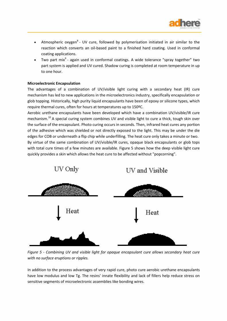
Microelectronic Encapsulation
The advantages of a combination of UV/visible light curing with a secondary heat (IR) cure
mechanism has led to new applications in the microelectronics industry, specifically encapsulation or
glob topping. Historically, high purity liquid encapsulants have been of epoxy or silicone types, which
require thermal cures, often for hours at temperatures up to 150ºC.
Aerobic urethane encapsulants have been developed which have a combination UV/visible/IR cure
mechanism.10 A special curing system combines UV and visible light to cure a thick, tough skin over
the surface of the encapsulant. Photo curing occurs in seconds. Then, infrared heat cures any portion
of the adhesive which was shielded or not directly exposed to the light. This may be under the die
edges for COB or underneath a flip chip while underfilling. The heat cure only takes a minute or two.
By virtue of the same combination of UV/visible/IR cures, opaque black encapsulants or glob tops
with total cure times of a few minutes are available. Figure 5 shows how the deep visible light cure
quickly provides a skin which allows the heat cure to be affected without "popcorning".
Figure 5 - Combining UV and visible light for opaque encapsulant cure allows secondary heat cure
with no surface eruptions or ripples.
In addition to the process advantages of very rapid cure, photo cure aerobic urethane encapsulants
have low modulus and low Tg. The resins' innate flexibility and lack of fillers help reduce stress on
sensitive segments of microelectronic assemblies like bonding wires.
New Applications
These are potential or actual applications which demonstrate some of the new uses for which photo
cure adhesives and coatings (with some of their unique properties) are being considered.
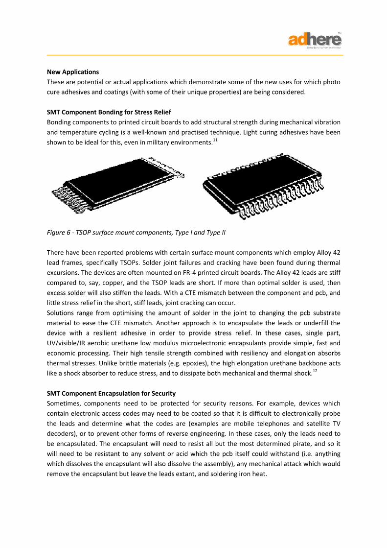
SMT Component Bonding for Stress Relief
Bonding components to printed circuit boards to add structural strength during mechanical vibration
and temperature cycling is a well-known and practised technique. Light curing adhesives have been
shown to be ideal for this, even in military environments.11
Figure 6 - TSOP surface mount components, Type I and Type II
There have been reported problems with certain surface mount components which employ Alloy 42
lead frames, specifically TSOPs. Solder joint failures and cracking have been found during thermal
excursions. The devices are often mounted on FR-4 printed circuit boards. The Alloy 42 leads are stiff
compared to, say, copper, and the TSOP leads are short. If more than optimal solder is used, then
excess solder will also stiffen the leads. With a CTE mismatch between the component and pcb, and
little stress relief in the short, stiff leads, joint cracking can occur.
Solutions range from optimising the amount of solder in the joint to changing the pcb substrate
material to ease the CTE mismatch. Another approach is to encapsulate the leads or underfill the
device with a resilient adhesive in order to provide stress relief. In these cases, single part,
UV/visible/IR aerobic urethane low modulus microelectronic encapsulants provide simple, fast and
economic processing. Their high tensile strength combined with resiliency and elongation absorbs
thermal stresses. Unlike brittle materials (e.g. epoxies), the high elongation urethane backbone acts
like a shock absorber to reduce stress, and to dissipate both mechanical and thermal shock.12
SMT Component Encapsulation for Security
Sometimes, components need to be protected for security reasons. For example, devices which
contain electronic access codes may need to be coated so that it is difficult to electronically probe
the leads and determine what the codes are (examples are mobile telephones and satellite TV
decoders), or to prevent other forms of reverse engineering. In these cases, only the leads need to
be encapsulated. The encapsulant will need to resist all but the most determined pirate, and so it
will need to be resistant to any solvent or acid which the pcb itself could withstand (i.e. anything
which dissolves the encapsulant will also dissolve the assembly), any mechanical attack which would
remove the encapsulant but leave the leads extant, and soldering iron heat.
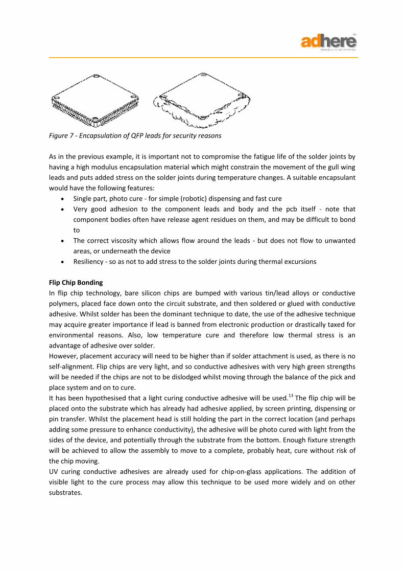
Figure 7 - Encapsulation of QFP leads for security reasons
As in the previous example, it is important not to compromise the fatigue life of the solder joints by
having a high modulus encapsulation material which might constrain the movement of the gull wing
leads and puts added stress on the solder joints during temperature changes. A suitable encapsulant
would have the following features:
Single part, photo cure - for simple (robotic) dispensing and fast cure
Very good adhesion to the component leads and body and the pcb itself - note that
component bodies often have release agent residues on them, and may be difficult to bond
to
The correct viscosity which allows flow around the leads - but does not flow to unwanted
areas, or underneath the device
Resiliency - so as not to add stress to the solder joints during thermal excursions
Flip Chip Bonding
In flip chip technology, bare silicon chips are bumped with various tin/lead alloys or conductive
polymers, placed face down onto the circuit substrate, and then soldered or glued with conductive
adhesive. Whilst solder has been the dominant technique to date, the use of the adhesive technique
may acquire greater importance if lead is banned from electronic production or drastically taxed for
environmental reasons. Also, low temperature cure and therefore low thermal stress is an
advantage of adhesive over solder.
However, placement accuracy will need to be higher than if solder attachment is used, as there is no
self-alignment. Flip chips are very light, and so conductive adhesives with very high green strengths
will be needed if the chips are not to be dislodged whilst moving through the balance of the pick and
place system and on to cure.
It has been hypothesised that a light curing conductive adhesive will be used.13 The flip chip will be
placed onto the substrate which has already had adhesive applied, by screen printing, dispensing or
pin transfer. Whilst the placement head is still holding the part in the correct location (and perhaps
adding some pressure to enhance conductivity), the adhesive will be photo cured with light from the
sides of the device, and potentially through the substrate from the bottom. Enough fixture strength
will be achieved to allow the assembly to move to a complete, probably heat, cure without risk of
the chip moving.
UV curing conductive adhesives are already used for chip-on-glass applications. The addition of
visible light to the cure process may allow this technique to be used more widely and on other
substrates.
References
1. Swanson, Peter, "Case Histories of Radiation Curing for Electronic Packaging", Proceedings
Nepcon West, Anaheim, CA (1996); also Soldering & Surface Mount Technology No. 24, pp.
19-24, October (1996)
2. Verguld, Martin, "Trends in Electronics Assembly Processes", Proceedings SMART Group
Second European Surface Mount Conference, Brighton, UK, November (1996)
3. Bachmann, Andrew, "Aerobic Adhesives III, Increasing Quality and Productivity with
Customization and Adhesive Process Integration", SME Technical Paper AD90-713 (1990)
4. Hnojewyj, Dr Olexander and Murdock, Mark, "Ultraviolet (UV) Curable Materials for Specific
Military Electronics Applications", Navy's Best Manufacturing Practices Workshop, (1989)
5. Swanson, Peter, "Case Histories of Radiation Curing for Electronic Packaging", Proceedings
Nepcon West, Anaheim, CA (1996)
6. Bachmann, Clai, "Expanding Capabilities with UV/Visible Light Cure Adhesives", Adhesives
Age, April (1995)
7. Bachmann, Andrew, "Aerobic Acrylic Adhesives", Adhesives Age, August (1982)
8. Cantor, Dr. Stephen; Huang, Farre and Orban, John, "Solvent-Free Aerobic Adhesives and
Coatings II - One Part, Room Temperature, Shadow Curing UV Conformal Coatings",
Proceedings Nepcon West, Anaheim, CA (1994)
9. Cantor, Dr Stephen, "Solvent-Free Aerobic Acrylic Adhesives and Coatings III - Two Part,
Room Temperature, Shadow Curing UV Conformal Coatings", Proceedings Nepcon West,
Anaheim, CA (1996)
10. Arnold, John and Forman, Samuel, "Low Stress Aerobic Urethanes Lower Costs for
Microelectronic Encapsulation", SME Technical Paper EE95-263, Adhesives '95 Conference,
Chicago, IL (1995)
11. Hnojewyj, Dr Olexander and Murdock, Mark, "Ultraviolet (UV) Curable Materials for Specific
Military Electronics Applications", Navy's Best Manufacturing Practices Workshop, (1989)
12. Jasne, Stanley, "Low-Modulii Polymers", Circuits Assembly, August (1995)
13. Schiebel, Gunter, "SMD Placement Machine Requirements for BGAs and Flip Chips",
Proceedings SMART Group Second European Surface Mount Conference, Brighton, UK,
November (1996)
Contact INTERTRONICS 17 Station Field Industrial Estate KIDLINGTON Oxfordshire OX5 1JD England t 01865 842842 e [email protected] www.intertronics.co.uk
© Peter Swanson, 1997
About adhere – better bonding from INTERTRONICS A unique solution designed to make life easy for designers and production specialists, adhere brings together our proven range of products for your high technology, high performance assembly requirements. Now you can specify and buy from one source with the confidence that everything will work together efficiently and cost-effectively, underpinned by our experience and expert advice. The adhere concept covers our range of industrial adhesives, encapsulants, coatings, sealants and tapes as well as the associated dispensing, curing and surface preparation equipment and materials used in the manufacturing and assembly processes. INTERTRONICS is dedicated to exceeding customer expectations by providing quality adhesive solutions to high technology, high performance assembly industries, incorporating outstanding levels of technical support and customer service. Visit the about us section of our website for more information. More questions? Please call us on 01865 842842 or email [email protected] Share with a colleague Please feel free to pass this white paper along to your interested friends and colleagues. Stay in touch! Please let us keep you up to date - fill in this form to receive Joined Up Thinking, a regular, simple e-mail containing ideas for the practitioner of high technology, high performance assembly.