Embed Size (px)
Citation preview
ADDENDUM NUMBER 2 TO MAINTENANCE MANUAL LBI-38671N
Refer to ECO#20034647
GENERAL
This addendum updates information about the Printed Wire Board (PWB) for UHF Transmitter Synthesizer Module Boards 19D902780G1, G3, G6-G8, 19D902779G1, G3, G6-G8, and 19D903483G1, G3, G6-G8, G300.
PRODUCTION CHANGES
On page 6 of the manual, update the production changes to include the following information:
Rev. 4A – Transmitter Synthesizer Board 19D902780G1, G3, G6-G8
Rev. 9A – Transmitter Synthesizer Board 19D902779G1
Rev. AA – Transmitter Synthesizer Board 19D902779G3
Rev. 8A – Transmitter Synthesizer Board 19D902779G6-G8
Rev. 2A – Transmitter Synthesizer Board 19D903483G1, G3, G6-G8, G300
Change Inductor L2 from 19A705470P24, Inductor, Fixed, SMT, 0.82uH, 5%, 450 MA, to 19A705470P28, Inductor, Fixed, SMT, 1.8uH, 5%, 450 MA.

M/A-COM Wireless Systems 221 Jefferson Ridge Parkway Lynchburg, Virginia 24501 (Outside USA, 434-385-2400) Toll Free 800-528-7711 www.macom-wireless.com Printed in U.S.A.
ADDENDUM NUMBER 1 TO MAINTENANCE MANUAL LBI-38671N
GENERAL
This addendum updates information about the Printed Wire Board (PWB) for UHF Transmitter Synthesizer Module Boards 19D902779G3, G6-G10 in Maintenance Manual LBI-38671.
CHANGES
On page 7 of the manual, update the production changes to include the following information:
Rev. 9A - Transmitter Synthesizer Board 19D902779G3
Rev. 7A - Transmitter Synthesizer Board 19D902779G6-G8
Rev. 4A - Transmitter Synthesizer Board 19D902779G9
Rev. 5A - Transmitter Synthesizer Board 19D902779G10
To improve efficiency during manufacturing, change 19D903361P1 and 19D903361P1R3 to 19D903361P1R4 (peelable mask removed from center of 19D903361P1R3).

Lynchburg, Virginia 24501 (Outside USA, 434-385-2400) Toll Free 800-528-7711 www.macom-wireless.com Printed in U.S.A.
M/A-COM Wireless Systems 221 Jefferson Ridge Parkway
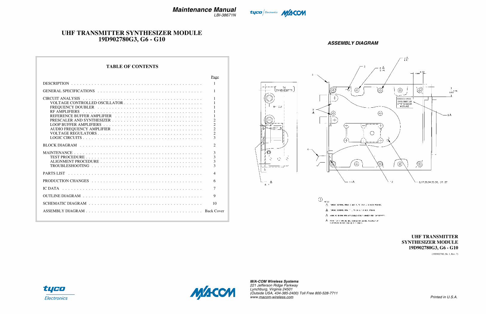
UHF TRANSMITTER SYNTHESIZER MODULE19D902780G3, G6 - G10
Maintenance ManualLBI-38671N
TABLE OF CONTENTS
Page
DESCRIPTION . . . . . . . . . . . . . . . . . . . . . . . . . . . . . . . . . . . . . . . . . . . . . 1
GENERAL SPECIFICATIONS . . . . . . . . . . . . . . . . . . . . . . . . . . . . . . . . . . . . 1
CIRCUIT ANALYSIS . . . . . . . . . . . . . . . . . . . . . . . . . . . . . . . . . . . . . . . . . 1VOLTAGE CONTROLLED OSCILLATOR . . . . . . . . . . . . . . . . . . . . . . . . . . . 1FREQUENCY DOUBLER . . . . . . . . . . . . . . . . . . . . . . . . . . . . . . . . . . . . 1RF AMPLIFIERS . . . . . . . . . . . . . . . . . . . . . . . . . . . . . . . . . . . . . . . . . 1REFERENCE BUFFER AMPLIFIER . . . . . . . . . . . . . . . . . . . . . . . . . . . . . . 1PRESCALER AND SYNTHESIZER . . . . . . . . . . . . . . . . . . . . . . . . . . . . . . . 2LOOP BUFFER AMPLIFIERS . . . . . . . . . . . . . . . . . . . . . . . . . . . . . . . . . . 2AUDIO FREQUENCY AMPLIFIER . . . . . . . . . . . . . . . . . . . . . . . . . . . . . . . 2VOLTAGE REGULATORS . . . . . . . . . . . . . . . . . . . . . . . . . . . . . . . . . . . . 2LOGIC CIRCUITS . . . . . . . . . . . . . . . . . . . . . . . . . . . . . . . . . . . . . . . . . 3
BLOCK DIAGRAM . . . . . . . . . . . . . . . . . . . . . . . . . . . . . . . . . . . . . . . . . . 2
MAINTENANCE . . . . . . . . . . . . . . . . . . . . . . . . . . . . . . . . . . . . . . . . . . . . 3TEST PROCEDURE . . . . . . . . . . . . . . . . . . . . . . . . . . . . . . . . . . . . . . . . 3ALIGNMENT PROCEDURE . . . . . . . . . . . . . . . . . . . . . . . . . . . . . . . . . . . 3TROUBLESHOOTING . . . . . . . . . . . . . . . . . . . . . . . . . . . . . . . . . . . . . . 3
PARTS LIST . . . . . . . . . . . . . . . . . . . . . . . . . . . . . . . . . . . . . . . . . . . . . . 4
PRODUCTION CHANGES . . . . . . . . . . . . . . . . . . . . . . . . . . . . . . . . . . . . . . 6
IC DATA . . . . . . . . . . . . . . . . . . . . . . . . . . . . . . . . . . . . . . . . . . . . . . . . 7
OUTLINE DIAGRAM . . . . . . . . . . . . . . . . . . . . . . . . . . . . . . . . . . . . . . . . . 9
SCHEMATIC DIAGRAM . . . . . . . . . . . . . . . . . . . . . . . . . . . . . . . . . . . . . . . 10
ASSEMBLY DIAGRAM . . . . . . . . . . . . . . . . . . . . . . . . . . . . . . . . . . . . . . . . Back Cover
UHF TRANSMITTERSYNTHESIZER MODULE
19D902780G3, G6 - G10(19D902780, Sh. 1, Rev. 7)
ASSEMBLY DIAGRAM
M/A-COM Wireless Systems221 Jefferson Ridge ParkwayLynchburg, Virginia 24501(Outside USA, 434-385-2400) Toll Free 800-528-7711www.macom-wireless.com Printed in U.S.A.
DESCRIPTION
The principle function of the Transmitter Synthesizer Mod-ule is to provide the RF excitation for input to the MASTR®III station power amplifier. The output of the synthesizer isa frequency modulated signal at the desired frequency. Themodule contains the following functional blocks:
• A voltage controlled oscillator,
• Frequency Doubler (Multiplier),
• A chain of integrated circuit RF Amplifiers,
• A reference buffer amplifier,
• Dual modulus prescaler and synthesizer integratedcircuits,
• Loop amplifiers and passive loop filter,
• An audio amplifier and a pre-modulation integra-tor.
• IC voltage regulators for +5 and -5 Vdc, a discretecomponent regulator for +8 Vdc, and an Opera-tional Amplifier regulator for +4 Vdc.
• Logic circuitry: address decoder, input signal gates,and a lock indicator circuit.
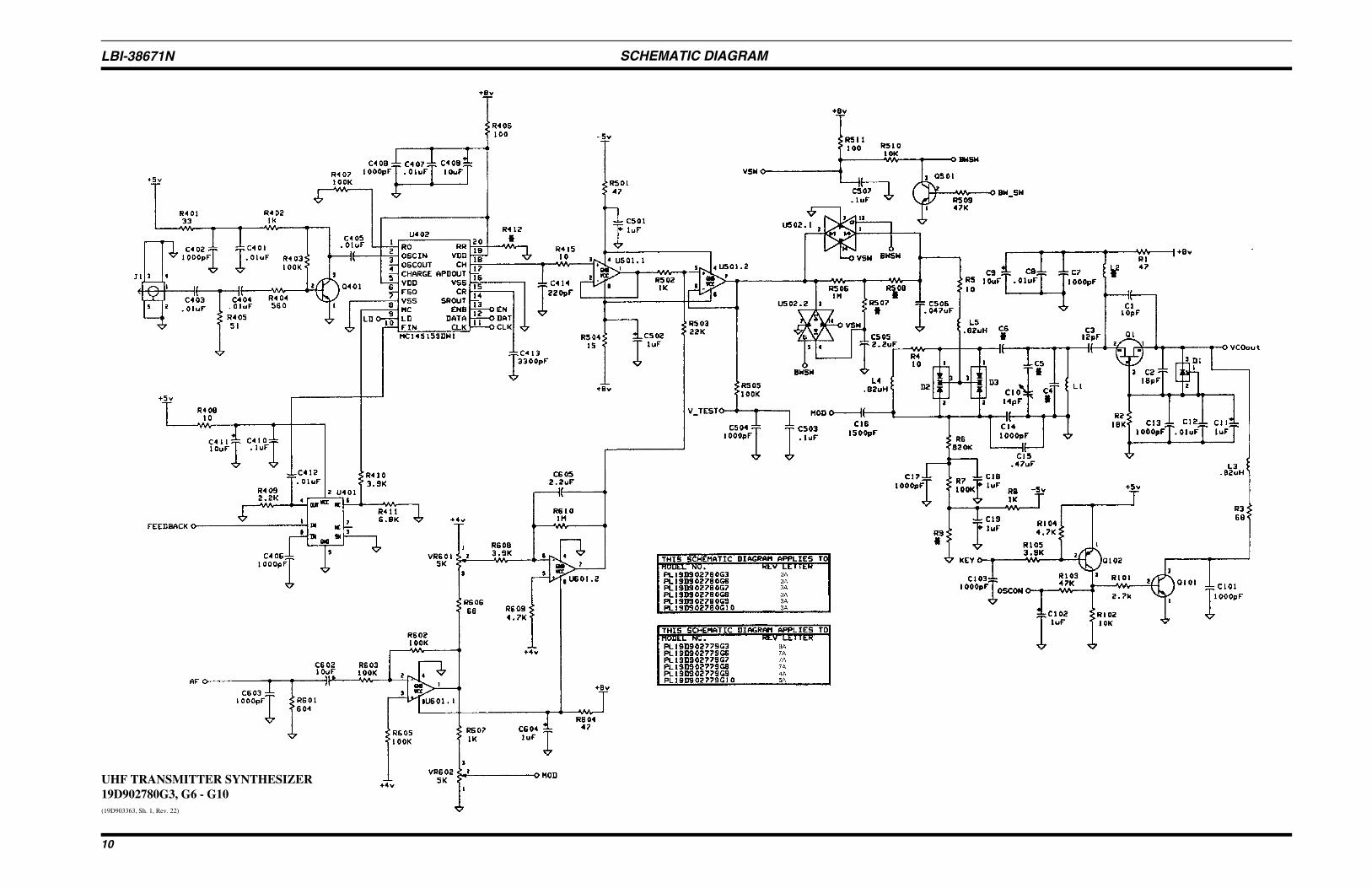
CIRCUIT ANALYSIS
VOLTAGE CONTROLLED OSCILLATOR
Transistor Q1 and associated circuitry form a low noiseVoltage Controlled Oscillator (VCO). Inductor L1 and asso-ciated capacitors form the oscillator resonant circuit (tank).The noise characteristic of this oscillator is dependent on theQ of this resonant circuit. The components used in the tankare specified to have especially high Q. Diode D1 aids insetting the bias point for low noise operation. (Any fieldreplacement of oscillator parts should use identical parts.)
Variable Capacitor C10 sets the fixed capacitance in thetank, and therefore sets the frequency range over which theoscillator can be voltage tuned.
The oscillator frequency is voltage tuned by the signal ap-plied through R5 and L5 to the two varicap diodes D2 andD3. Additionally, audio modulation is applied as an AFvoltage to the two varicap diodes. This AF voltage varies theoscillator frequency at an audio rate (i.e., it frequency modu-lates the oscillator). Low frequency audio is applied alongwith the varicap control voltage through R5 and L5 whilehigh frequency audio (MOD) is applied via C16.
Resistors R6 through R9 provide a two volt negative bias onthe varicap diodes.
Transistors Q101 and Q102 and associated circuitry form theoscillator enable switch. This switch allows the station con-trol circuitry to turn the VCO ON or OFF via the ANT_RELline. Setting the ANT_REL line to a logic low causes Q102to conduct. The five (5) volt output at Q102 collector(OSCON) enables the fault indicator gates, U705-3 andU705-4, and turns on Q101. Q101 starts to conduct, provid-ing a ground path for Q1. This turns ON the VCO.
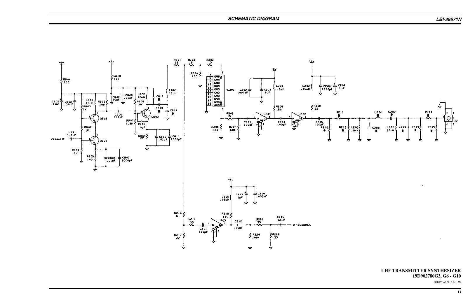
FREQUENCY DOUBLER
Transistors Q801 and Q802 form a buffer stage to drivetransistor multiplier Q803. The buffer isolates VCO Q1 fromloading effects which could degrade oscillator loaded Q andhence noise performance. Transistor multiplier Q803 istuned to pass the second harmonic of the VCO output andserves as a frequency doubler. Tank elements L802, C812-C814 and L803 form a resonant circuit and matching net-work to drive resistive splitter R201-R204.
RF AMPLIFIERS
The RF chain begins with resistive splitter R201-R204 andR216-R218. The output of the splitter at R203 is attenuatedby 10 dB and provides impedance matching helical filterFL201, which is tuned to pass the fundamental while reject-ing harmonics by approximately 40 dB. The output of FL201is fed thru resistive pad R205-R207 to MMIC AmplifierU201 which operates in compression. U201 drives outputamplifier U202 into compression. The output amplifier isfollowed by a bandpass filter (C208-C210, L203-L205) andresistive attenuators (R210-R215). The final output at thefront panel BNC (J2) is nominally 11.5 dBm, and drives thestation Power Amp.
The other output of the resistive splitter at R218 is attenuatedby 20 dB and drives buffer amp U203 into compression.U203 drives the synthesizer prescaler providing a feedbacksignal for the synthesizer phase locked loop.
REFERENCE BUFFER AMPLIFIER
Transistor Q401 and associated components from a bufferamplifier for the reference oscillator signal. (The referenceoscillator signal is produced by the receiver synthesizermodule of a MASTR III station.) The 0 dBm referenceoscillator signal is fed through the front panel BNC J1.Resistor R405 provides a 50 ohm load to the referenceoscillator. The output of the Reference Buffer Amplifier isfed directly to the synthesizer integrated circuit. The outputlevel at TP9 is approximately 3 volts peak to peak.
Copyright © 1992-2004, M/A-COM, Inc. All rights reserved.
TABLE 1: GENERAL SPECIFICATIONS
ITEM SPECIFICATION
FREQUENCY RANGE 450-470 MHz (G3)425-450 MHz (G7)403-430 MHz (G6)380-400 MHz (G8)470-494 MHz (G9)490-512 MHz (G10)
CHANNEL SPACING 6.25 kHz
RF POWER OUT (50 Ohm load) 10 to 13 dBm(10 to 20 mW)
RF HARMONICS < -30 dBc
NON-HARMONIC SPURS1 to 200 MHz < - 90 dBc200 MHz to 1 GHz < - 60 dBc
CARRIER ATTACK TIME <25 mSec
REFERENCE INPUTinput level 0 dBm ±1.5dBinput impedance 50 Ohmfrequency 5 to 17.925 MHz (must be integer divisible by
channel spacing)
MODULATION SENSITIVITY 5 kHz peak dev/1 Vrms, Adjustable
AF INPUT IMPEDANCE 600 Ohm
AF RESPONSE10 Hz ±1.5 dB1000 Hz0 dB reference3 kHz ±1.5 dB
10 Hz SQUARE WAVE MODULATION <10%Sq wave droop
HUM & NOISE -55 dB
POWER REQUIREMENTS 13.8 Vdc @ 275 mA-12.0 Vdc @ 10 mA
This manual is published by M/A-COM, Inc., without any warranty. Improvements and changes to this manual necessitated by typographical errors, inaccuracies of current information, or improvements to programsand/or equipment, may be made by M/A-COM, Inc., at any time and without notice. Such changes will be incorporated into new editions of this manual. No part of this manual may be reproduced or transmitted inany form or by any means, electronic or mechanical, including photocopying and recording, for any purpose, without the express written permission of M/A-COM, Inc.
CREDITS
MASTR and EDACS are registered trademarks of M/A-COM, Inc.
All other brand and product names are trademarks, registered trademarks, or service marks of their respective holders.
LBI-38671N
1
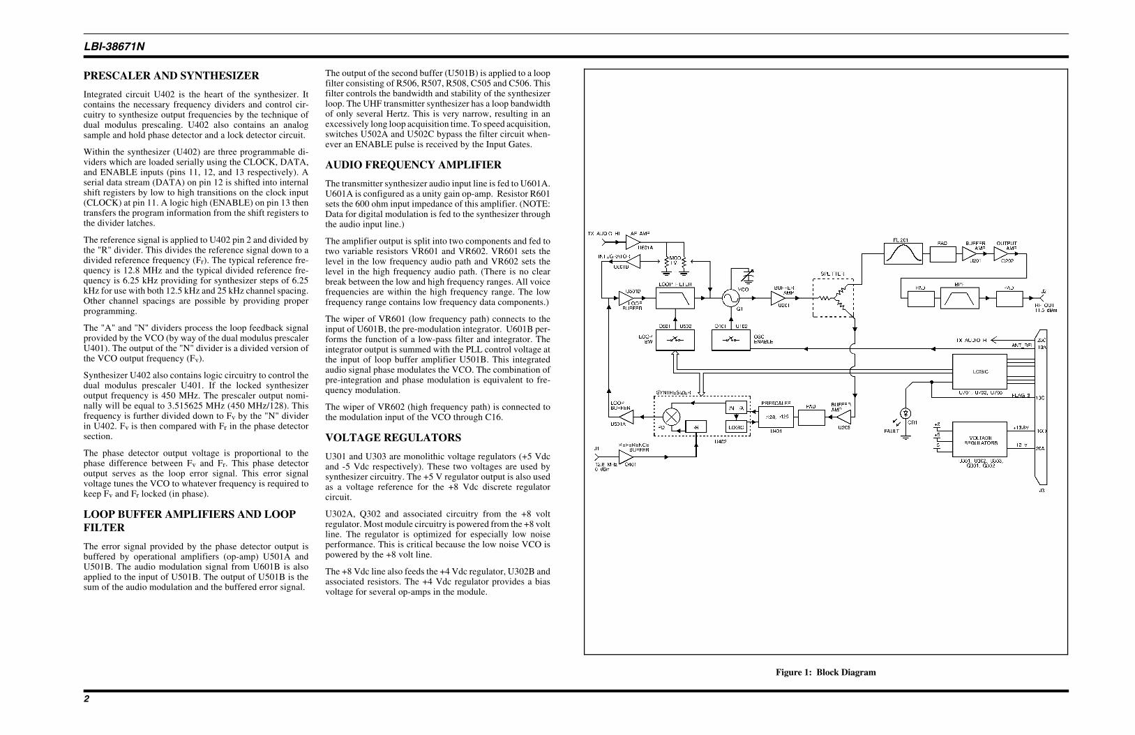
PRESCALER AND SYNTHESIZER
Integrated circuit U402 is the heart of the synthesizer. Itcontains the necessary frequency dividers and control cir-cuitry to synthesize output frequencies by the technique ofdual modulus prescaling. U402 also contains an analogsample and hold phase detector and a lock detector circuit.
Within the synthesizer (U402) are three programmable di-viders which are loaded serially using the CLOCK, DATA,and ENABLE inputs (pins 11, 12, and 13 respectively). Aserial data stream (DATA) on pin 12 is shifted into internalshift registers by low to high transitions on the clock input(CLOCK) at pin 11. A logic high (ENABLE) on pin 13 thentransfers the program information from the shift registers tothe divider latches.
The reference signal is applied to U402 pin 2 and divided bythe "R" divider. This divides the reference signal down to adivided reference frequency (Fr). The typical reference fre-quency is 12.8 MHz and the typical divided reference fre-quency is 6.25 kHz providing for synthesizer steps of 6.25kHz for use with both 12.5 kHz and 25 kHz channel spacing.Other channel spacings are possible by providing properprogramming.
The "A" and "N" dividers process the loop feedback signalprovided by the VCO (by way of the dual modulus prescalerU401). The output of the "N" divider is a divided version ofthe VCO output frequency (Fv).
Synthesizer U402 also contains logic circuitry to control thedual modulus prescaler U401. If the locked synthesizeroutput frequency is 450 MHz. The prescaler output nomi-nally will be equal to 3.515625 MHz (450 MHz/128). Thisfrequency is further divided down to Fv by the "N" dividerin U402. Fv is then compared with Fr in the phase detectorsection.
The phase detector output voltage is proportional to thephase difference between Fv and Fr. This phase detectoroutput serves as the loop error signal. This error signalvoltage tunes the VCO to whatever frequency is required tokeep Fv and Fr locked (in phase).
LOOP BUFFER AMPLIFIERS AND LOOP FILTER
The error signal provided by the phase detector output isbuffered by operational amplifiers (op-amp) U501A andU501B. The audio modulation signal from U601B is alsoapplied to the input of U501B. The output of U501B is thesum of the audio modulation and the buffered error signal.
The output of the second buffer (U501B) is applied to a loopfilter consisting of R506, R507, R508, C505 and C506. Thisfilter controls the bandwidth and stability of the synthesizerloop. The UHF transmitter synthesizer has a loop bandwidthof only several Hertz. This is very narrow, resulting in anexcessively long loop acquisition time. To speed acquisition,switches U502A and U502C bypass the filter circuit when-ever an ENABLE pulse is received by the Input Gates.
AUDIO FREQUENCY AMPLIFIER
The transmitter synthesizer audio input line is fed to U601A.U601A is configured as a unity gain op-amp. Resistor R601sets the 600 ohm input impedance of this amplifier. (NOTE:Data for digital modulation is fed to the synthesizer throughthe audio input line.)
The amplifier output is split into two components and fed totwo variable resistors VR601 and VR602. VR601 sets thelevel in the low frequency audio path and VR602 sets thelevel in the high frequency audio path. (There is no clearbreak between the low and high frequency ranges. All voicefrequencies are within the high frequency range. The lowfrequency range contains low frequency data components.)
The wiper of VR601 (low frequency path) connects to theinput of U601B, the pre-modulation integrator. U601B per-forms the function of a low-pass filter and integrator. Theintegrator output is summed with the PLL control voltage atthe input of loop buffer amplifier U501B. This integratedaudio signal phase modulates the VCO. The combination ofpre-integration and phase modulation is equivalent to fre-quency modulation.
The wiper of VR602 (high frequency path) is connected tothe modulation input of the VCO through C16.
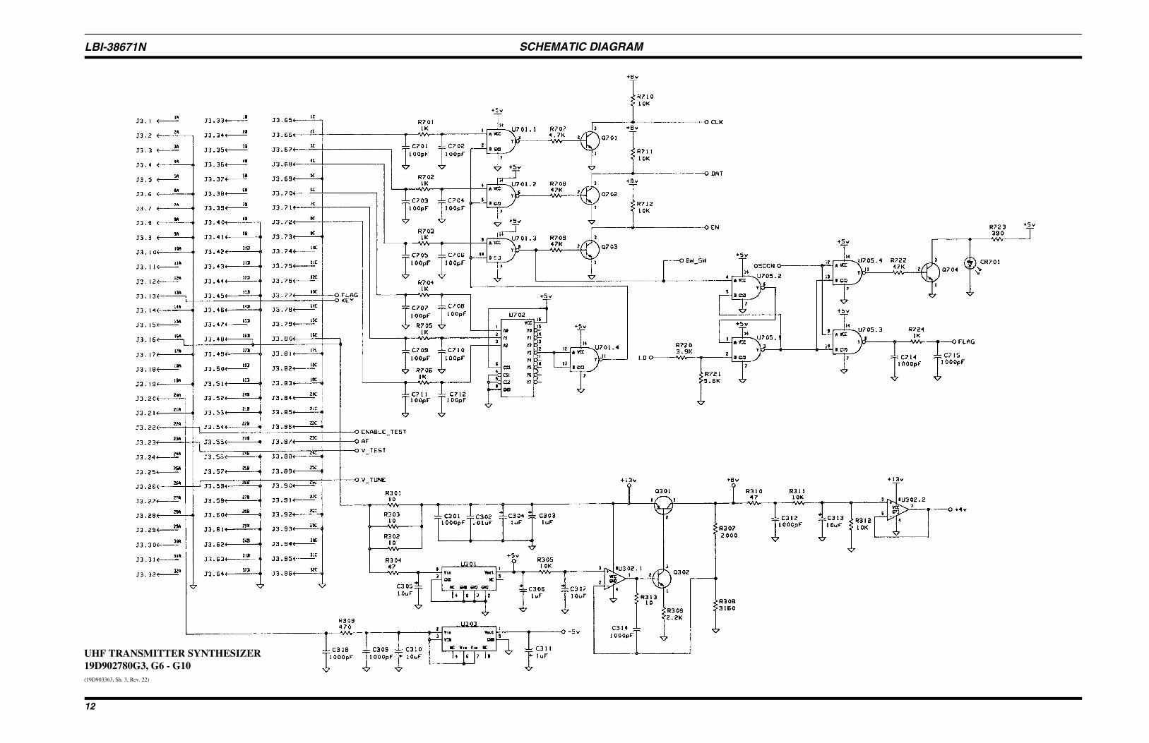
VOLTAGE REGULATORS
U301 and U303 are monolithic voltage regulators (+5 Vdcand -5 Vdc respectively). These two voltages are used bysynthesizer circuitry. The +5 V regulator output is also usedas a voltage reference for the +8 Vdc discrete regulatorcircuit.
U302A, Q302 and associated circuitry from the +8 voltregulator. Most module circuitry is powered from the +8 voltline. The regulator is optimized for especially low noiseperformance. This is critical because the low noise VCO ispowered by the +8 volt line.
The +8 Vdc line also feeds the +4 Vdc regulator, U302B andassociated resistors. The +4 Vdc regulator provides a biasvoltage for several op-amps in the module.
Figure 1: Block Diagram
LBI-38671N
2
LOGIC CIRCUITS
Logic circuitry (other than that inside the synthesizer IC -U402) consists of the following:
• An address decoder
• Input gates and level shifters
• Lock Indicator circuitry
The address decoder, U702, enables the Input Gates when theA0, A1, and A2 input lines receive the proper logic code (110for the transmitter synthesizer). After receiving the propercode, Y3 (U702-12) sends a logic low signal to U701C. U701Cacts as an inverter and uses the logic high output to turn onInput Gates U701A, U701B, and U701D. The Input Gatesallow the clock, data and enable information to pass on to thesynthesizer via the level shifters. The Level Shifter TransistorsQ701, Q702 and Q703 convert the 5 volt gate logic level to the8 volt logic level required by the synthesizer U402.
The Fault Indicator circuitry indicates when the synthesizer isin an out-of-lock condition. The fault detector latches, U705Aand U705B are reset by the enable pulse during initial loadingof data into the synthesizer. If at any time afterwards the lockdetector signal (LD) goes low, the high output of U705B willcause the output of gates U705C and U705D to go low. Thelow output from U705C causes Q704 to conduct turning on thefront panel LED (CR701). The output of U705D (FLAG) isconnected to J3-13C for external monitoring of the SynthesizerModule. A logic low on the FLAG line indicates an out-of-lockcondition.
MAINTENANCE
RECOMMENDED TEST EQUIPMENT
The following test equipment is required to test the synthesizerModule:
• RF signal source for 12.8 MHz, 0 dBm reference(included with item 10)
• AF Generator or Function Generator
• Modulation Analyzer; HP 8901A, or equivalent, or aUHF receiver
• Oscilloscope; 20 MHz
• DC Meter; 10 meg ohm (for troubleshooting)
• Power Supply; 13.8 Vdc @ 350 mA
• 12.0 Vdc @ 25 mA
• Spectrum Analyzer; 0-1 GHz
• Frequency Counter; 10 MHz - 500 MHz
• Personal Computer (IBM PC compatible) to load fre-quency data
• Service Parts Kit, (TQ-0650), (includes software forloading frequency data)
TEST PROCEDURE
(Steps 5, 6, and 7 can be done using a modulation analyzeror UHF receiver with 750 µs de-emphasis switchable in orout.)
1. Program synthesizer at 470.0 (G3), 430 (G6), 450(G7), 400 (G8), 494 (G9) or 512 (G10) MHz usingthe System Module personality or test software ifusing RF Test Fixture TQ-0650.
Verify lock (flag = high).Verify front panel LED is off.
2. Measure output frequency.
Verify frequency = 470.0000 (G3), 425.000(G6) or 450.000 (G7) MHz, 400.000 (G8),494.000 (G9) or 512.000 (G10) ±200 Hz.
3. Measure harmonic content.
Verify 2nd harmonic is < -30 dBc.
4. Measure RF power output into 50 ohm load.
Verify 10 to 13 dBm (10 to 20 mW).
5. Measure AF distortion with standard modulating sig-nal input.
Verify <2.5%.
6. Measure Hum and Noise relative to 0.44 kHz averagedeviation, (de-emphasis on).
Verify < -55dB.
7. Measure AF response at 300 Hz, 1 kHz (ref) and 3kHz, (de-emphasis off).
Verify within ±1.5 dB with respect to 1 kHzreference.
8. Verify lock at different frequencies.
a. Program synthesizer at 380 (G8), 450 (G3),403 (G6), 425 (G7), 470 (G9) or 492 (G10)MHz. Verify LED is off.
b. Program synthesizer at 385 (G8), 455 (G3),408.5 (G6), 430 (G7), 476 (G9) or 497 (G10)MHz. Verify LED is off.
c. Program synthesizer at 395 (G8), 465 (G3),419.5 (G6), 445 (G7), 488 (G9) or 507 (G10)MHz. Verify LED is off.
d. Program synthesizer at 400 (G8), 470 (G3),425 (G6), 450 (G7), 494 (G9) or 512 (G10)MHz. Verify LED is off.
ALIGNMENT PROCEDURE
1. Apply +13.8 Vdc and -12 Vdc. Verify the currentdrain on the 13.8 volt supply is <300mA and thecurrent drain on the -12 volt supply is <20 mA.
2. Program the synthesizer at 380 (G8), 450 (G3), 403(G6), 425 (G7), 470 (G9) or 492 (G10) MHz. Adjusttrimmer C10 until Vtest (23A) reads 2.5 (G3, G8),2.0 (G6, G7, G9) or 3.0 (G10) ±0.05Vdc.
3. Program synthesizer at 460.0 (G3), 390.0 (G8), 414(G6) or 437.5 (G7), 482 (G9) or 502 (G10) MHz forthe following three adjustments:
• Set VR602 for 4.5 kHz peak deviation with a stand-ard modulating signal applied to the audio input.
• Set VR601 for 4.5 kHz peak deviation with 1.0Vrms, 10 Hz (or 7 Hz for G3) sine wave audioapplied to module AF input.
• Apply a 10 Hz 1.4 Vpk square wave to module AFinput. Adjust VR601 slightly for the flattest de-modulated square wave using a modulation ana-lyzer or receiver (no de-emphasis) and anoscilloscope. The maximum net variation in voltageover 1/2 cycle is 5%.
TROUBLESHOOTING
A troubleshooting guide is provided showing typical meas-urements at the various test points.
FL201 has been aligned at the vendor to meet passbandand stopband specifications and is not be be realigned bythe factory or field technicians.
WARNING
This adjustment is critical for EDACS® applica-tion and must be reset at customer frequency.
NOTE
FL201 has been aligned at the vendor to meet passbandand stopband specifications and is not be be realigned bythe factory or field technicians.
WARNING
SERVICE NOTES
The following service information applies whenaligning, testing, or troubleshooting the TX Synthe-sizer:
• Standard Modulating Signal = 1 kHz sinusoidalvoltage, 0.6 Vrms at the module input terminals(600 ohm Rin).
• The input audio level for setting the 4.5 kHz or 10Hz (or 7 Hz) deviation should always be 1.00 Vrms.
• In the modulation adjustment, any reference to 0.6Vrms refers to the voltage level for a STANDARDsignal, usually 60% (3.0 kHz) of maximum devia-tion. The 0.6 Vrms will produce 60% of full devia-tion.
• Logic Levels:Logic 1 = High = 4.5 to 5.5 VdcLogic 0 = Low = 0 to 0.5 Vdc
• Transmitter Synthesizer Address = A0 A1 A2 = 110
• Synthesizer data input stream is as follows:
14-bit "R" divider most significant bit(MSB) = R13 through "R" divider least sig-nificant bit (LSB) = R0
10-bit "N" divider MSB = N9 through "N"divider LSB = N0
7-bit "A" divider MSB = A6 through "A"divider LSB = A0
Single High Control Bit (last bit)
Latched When Control Bit = 1
DATA ENTRY FORMAT
Latched When
Control Bit = 1
Data in Last A0 A6 N0 N9 R0 R13Bit LSB – – – – – MSB LSB – – – – MSB LSB
For the transmitter synthesizer, 5 kHz chan-nel spacingR = 2560N = integer part of (frequency in kHz)/(320)A = (frequency in kHz)/(5) - 64*NAll numbers must be converted to binary.
• ANT_REL line must be logic low (0V) in order tolock synthesizer.
• Synthesizer lock is indicated by the extinguishingof the front panel LED indicator and a logic high onthe fault flag line (J3 pin 13C).
• Always verify synthesizer lock after each new dataloading.
Control B
LBI-38671N
3
PARTS LIST
SYMPTOM CHECK(CORRECT READINGS SHOWN)
INCORRECT READING INDICATESDEFECTIVE COMPONENT
Synthesizer Fails To Lock Check DC voltages+5 V @ U301 Pin 1+8 V @ Q301 collector
-5 V @ U303 Pin 1
U301 or associated componentsU302, Q301, Q302 or associatedcomponentsU303 or associated components
Check 12.8 MHz reference signal3V P-P, 12.8 MHz @ U402 Pin 2
No reference signal to front panel BNC orQ401
Check oscillator signal
11.5 ±1.5 dBm 435 to 485 MHz at front panel BNC
Proceed to "Low/No RF output" below
Check prescaler output
1V P-P, 3.5 MHz @ U401 Pin 4 U202, U401
Check CLOCK, DATA, ENABLE
While loading frequency data intosynthesizer Check 8V logicsignals @ Pins 11, 12, 13 of U402
Wrong address or U701, U702, Q701, Q702, Q703
Check Phase detector output
6.25 kHz random signal @ U501 Pin 7
U402, U501
Low/No RF Output Check oscillator
LESS than 0.5 Vdc @ collector of Q101
Synthesizer not keyed (low on ANT relayline) or Q101, Q102
Check RF chain
No Modulation Check AF amplifier
Apply 1V, 1 kHz signal toTX/Audio/Hi
U601
Check 1V signal @ U601 Pin 1
TROUBLESHOOTING GUIDE UHF TRANSMITTER SYNTHESIZER MODULE19D902780G3, G6 - G10
ISSUE 12
*COMPONENTS, ADDED, DELETED OR CHANGED BY PRODUCTION CHANGES
SYMBOL PART NO. DESCRIPTION
- - - - - - - - - MISCELLANEOUS - - - - - - - - -
2 19D902508P4 Chassis.
3 19D902509P10 Cover.
4 19D902555P1 Handle.
6 19A702381P506 Screw, thread forming: TORX, No. M3.5-.6 x 6.
7 19A702381P513 Screw, thread forming: TORX, No. M3.5 - 0.6 X 13.
9 19B802690P2 RF Shielding Grommet
11 19A702381P508 Screw, thd. form: No. 3.5-0.6 x 8.
12 19D902824P1 Casting.
AG102834V1 Gasket, EMI Shield
TRANSMITTER SYNTHESIZER BOARD19D902779G3, G6 - G10
- - - - - - - - - - CAPACITORS - - - - - - - - -
C1 19A702236P25 Ceramic: 10 pF + or -.5 pF, 50 VDCW, temp coef+ or -30 PPM/°C.
C2 19A702236P32 Ceramic: 18 pF + or -5%, 50 VDCW, temp coef 0 ++ or or -30 PPM
C3 19A702236P28 Ceramic: 12 pF + or - 5%, 50 VDCW, temp coef 0+ or -30 PPM.
C4 19A702236P10 Ceramic: 2.2pF + or - 0.25pF, 50 VDCW, temp coef 0 +or - 30 PPM/°C (Used in G3).
C4 19A702236P1 Ceramic: 0.5pF + or - 0.25pF, 50 VDCW, temp coef 0 +or - 30 PPM/°C (Used in G8).
C4 19A702236P17 Ceramic: 4.7pF + or - 5%, 50 VDCW, temp coef 0 + or -60 PPM/°C (Used in G9).
C4 19A702236P11 Ceramic: 2.7pF + or - 5%, 50 VDCW, temp coef 0 + or -30 PPM/°C (Used in G10).
C5 19A702236P17 Ceramic: 4.7pF + or - 5%, 50 VDCW, temp coef 0 + or -60 PPM/°C (Used in G3, G6 & G8 through G10).
C5 19A702236P25 Ceramic: 10pF + or - 0.25pF, 50 VDCW, temp coef 0 +or - 30 PPM/°C (Used in G7).
C6 19A702236P28 Ceramic: 12 pF + or - 5%, 50 VDCW, temp coef 0+ or -30 PPM. (Used in G3).
C6 19A702236P30 Ceramic: 15 pF + or -5%, 50 VDCW, temp coef 0 +or -30 PPM/°C. (Used in G6 & G7).
C6 19A702236P32 Ceramic: 18 pF + or - 5%, 50 VDCW, temp coef 0+ or -30 PPM. (Used in G8).
*C6 19A702236P28 Ceramic: 12 pF + or -5%, 50 VDCW, temp coef 0+ or -30 PPM/°C. (Used in G9 & G10).
C7 19A702061P99 Ceramic: 1000 pF + or -5%, 50 VDCW, temp coef 0+ or -30 PPM/°C.
C8 19A702052P14 Ceramic: 0.01 uF + or - 10%, 50 VDCW.
C9 19A705205P6 Tantalum: 10 uF, 16 VDCW; sim to Sprague 293D.
C10 19A134227P5 Variable: 1.5 to 14 pF, 100 VDCW.
C11 19A705205P2 Tantalum: 1 uF, 16 VDCW; sim to Sprague 293D.
C12 19A702052P14 Ceramic: 0.01 uF + or - 10%, 50 VDCW.
C13 19A702061P99 Ceramic: 1000 pF + or -5%, 50 VDCW, temp coef 0and + or -30 PPM/°C.C14
*C15 19A700004P6 Metallized polyester: 4.7 uF + or - 10%, 63 VDCW.
*C16 19A702052P106 Ceramic: 1500 pF + or -5%, 50 VDCW.
C17 19A702061P99 Ceramic: 1000 pF + or -5%, 50 VDCW, temp coef 0+ or -30 PPM/°C.
C18 19A705205P2 Tantalum: 1 uF, 16 VDCW; sim to Sprague 293D.andC19
C101 19A702061P99 Ceramic: 1000 pF + or -5%, 50 VDCW, temp coef 0+ or -30 PPM/°C.
C102 19A705205P2 Tantalum: 1 uF, 16 VDCW; sim to Sprague 293D.
C103 19A702061P99 Ceramic: 1000 pF + or -5%, 50 VDCW, temp coef 0+ or -30 PPM/°C.
SYMBOL PART NO. DESCRIPTION
C201 19A702061P61 Ceramic: 100 pF + or - 5%, 50 VDCW, temp coef 0+ or - 30 PPM.
C202 19A702061P99 Ceramic: 1000 pF + or -5%, 50 VDCW, temp coef 0+ or -30 PPM/°C.
C203 19A705205P2 Tantalum: 1 uF, 16 VDCW; sim to Sprague 293D.
C204 19A702061P61 Ceramic: 100 pF + or - 5%, 50 VDCW, temp coef 0and + or - 30 PPM.C205
C206 19A702061P99 Ceramic: 1000 pF + or -5%, 50 VDCW, temp coef 0+ or -30 PPM/°C.
C207 19A705205P2 Tantalum: 1 uF, 16 VDCW; sim to Sprague 293D.
C208 19A702236P25 Ceramic: 10pF + or - 5%, 50 VDCW, temp coef 0 + or -30 PPM/°C (Used in G3).
C208 19A702236P28 Ceramic: 12pF + or - 5%, 50 VDCW, temp coef 0 + or -30 PPM/°C.
C209 19A702236P9 Ceramic: 1.8pF + or - 0.25 pF, 50 VDCW, temp coef 0 +or - 30 PPM/°C (Used in G3).
C209 19A702236P10 Ceramic: 2.2pF + or -0.25 pF, 50 VDCW, temp coef 0 +or - 30 PPM/°C (Used in G6, G7, G8).
C209 19A702236P8 Ceramic: 1.8pF + or -0.25 pF, 50 VDCW, temp coef 0 +or - 30 PPM/°C (Used in G9).
C209 19A702236P9 Ceramic: 1.5pF + or -0.25 pF, 50 VDCW, temp coef 0 +or - 30 PPM/°C (Used in G10).
C210 19A702236P25 Ceramic: 10pF + or - 5%, 50 VDCW, temp coef 0 + or -30 PPM (Used in G3).
C210 19A702236P28 Ceramic: 12pF + or - 5%, 50 VDCW, temp coef 0 + or -30 PPM/°C.
C211 19A702061P61 Ceramic: 100 pF + or - 5%, 50 VDCW, temp coef 0and + or - 30 PPM.C212
C213 19A705205P2 Tantalum: 1 uF, 16 VDCW; sim to Sprague 293D.
C214 19A702061P99 Ceramic: 1000 pF + or -5%, 50 VDCW, temp coef 0+ or -30 PPM/°C.
C215 19A702061P61 Ceramic: 100 pF + or - 5%, 50 VDCW, temp coef 0+ or - 30 PPM.
C301 19A702061P99 Ceramic: 1000 pF + or -5%, 50 VDCW, temp coef 0+ or -30 PPM/°C.
C302 19A702052P14 Ceramic: 0.01 uF + or - 10%, 50 VDCW.
C303 19A705205P2 Tantalum: 1 uF, 16 VDCW; sim to Sprague 293D.andC304
C305 19A705205P7 Tantalum: 10 uF, 25 VDCW; sim to Sprague 293D.
C306 19A705205P2 Tantalum: 1 uF, 16 VDCW; sim to Sprague 293D.
C307 19A705205P6 Tantalum: 10 uF, 16 VDCW; sim to Sprague 293D.
C308 19A702061P99 Ceramic: 1000 pF + or -5%, 50 VDCW, temp coef 0and + or -30 PPM/°C.C309
C310 19A705205P6 Tantalum: 10 uF, 16 VDCW; sim to Sprague 293D.
C311 19A705205P2 Tantalum: 1 uF, 16 VDCW; sim to Sprague 293D.
C312 19A702061P99 Ceramic: 1000 pF + or -5%, 50 VDCW, temp coef 0+ or -30 PPM/°C.
C313 19A705205P6 Tantalum: 10 uF, 16 VDCW; sim to Sprague 293D.
C314 19A702061P99 Ceramic: 1000pF + or - 5%, 50 VDCW, temp coef 0 + or -30 PPM/°C.
C401 19A702052P14 Ceramic: 0.01 uF + or - 10%, 50 VDCW.
C402 19A702061P99 Ceramic: 1000 pF + or -5%, 50 VDCW, temp coef 0+ or -30 PPM/°C.
C403 19A702052P14 Ceramic: 0.01 uF + or - 10%, 50 VDCW.thruC405
C406 19A702061P99 Ceramic: 1000 pF + or -5%, 50 VDCW, temp coef 0+ or -30 PPM/°C.
C407 19A702052P14 Ceramic: 0.01 uF + or - 10%, 50 VDCW.
C408 19A702061P99 Ceramic: 1000 pF + or -5%, 50 VDCW, temp coef 0+ or -30 PPM/°C.
C409 19A705205P6 Tantalum: 10 uF, 16 VDCW; sim to Sprague 293D.
C410 19A702052P26 Ceramic: 0.1uF + or - 10%, 50 VDCW
LBI-38671N
4
PARTS LIST
SYMBOL PART NO. DESCRIPTION
C411 19A705205P6 Tantalum: 10 uF, 16 VDCW; sim to Sprague 293D.
C412 19A702052P14 Ceramic: 0.01 uF + or - 10%, 50 VDCW.
C413 19A702052P108 Ceramic: 0.01 uF + or -10%, 50 VDCW.
C414 19A702061P69 Ceramic: 220 pF + or -5%, 50 VDCW, temp coef 0+ or -30 PPM/°C.
C501 19A705205P2 Tantalum: 1 uF, 16 VDCW; sim to Sprague 293D.
C502 19A705205P2 Tantalum: 1 uF, 16 VDCW; sim to Sprague 293D.
C503 19A702052P33 Ceramic: 0.1 uF + or -10%, 50 VDCW.
C504 19A702061P99 Ceramic: 1000 pF + or -5%, 50 VDCW, temp coef 0+ or -30 PPM/°C.
C505 19A703684P3 Metalized polyester: 2.2 uF + or - 10$, 50 VDCW.
C506 19A703902P3 Metal: 0.047 uF + or -10%, 50 VDCW.
C507 19A702052P33 Ceramic: 0.1 uF + or -10%, 50 VDCW.
C602 19A705205P6 Tantalum: 10 uF, 16 VDCW; sim to Sprague 293D.
C603 19A702061P99 Ceramic: 1000 pF + or -5%, 50 VDCW, temp coef 0+ or -30 PPM/°C.
C604 19A705205P2 Tantalum: 1 uF, 16 VDCW; sim to Sprague 293D.
C605 19A703684P3 Metalized polyester: 2.2 uF + or - 10$, 50 VDCW.
C701 19A702061P61 Ceramic: 100 pF + or - 5%, 50 VDCW, temp coef 0thru + or - 30 PPM.C712
C714 19A702061P99 Ceramic: 1000 pF + or -5%, 50 VDCW, temp coef 0and + or -30 PPM/°C.C715
C801 19A702061P4 Ceramic: 1.8 pF + or - 0.5 pF, 50 VDCW, tempor - 250 PPM.
C802 19A705205P6 Tantalum: 10 uF, 16 VDCW; sim to Sprague 293D.
C803 19A702052P14 Ceramic: 0.01 uF + or - 10%, 50 VDCW.andC804
C805 19A702061P99 Ceramic: 1000 pF + or -5%, 50 VDCW, temp coef 0+ or -30 PPM/°C.
C806 19A702061P65 Ceramic: 150 pF + or -5%, 50 VDCW, temp coef 0+ or -30 PPM/°C.
C807 19A705205P6 Tantalum: 10 uF, 16 VDCW; sim to Sprague 293D.
C808 19A702052P14 Ceramic: 0.01 uF + or - 10%, 50 VDCW.
C809 19A702061P13 Ceramic: 10 pF + or - 5%, 50 VDCW, temp coef 0+ or - 30 PPM.
C810 19A702052P14 Ceramic: 0.01 uF + or - 10%, 50 VDCW.
C811 19A702061P99 Ceramic: 1000 pF + or -5%, 50 VDCW, temp coef 0+ or -30 PPM/°C.
C812 19A702061P13 Ceramic: 3.3 pF + or - 0.25 pF, tempor - 30 PPM/°C. (Used in G8).
C812 19A702061P5 Ceramic: 2.2 pF + or - 0.5 pF, 50 VDCW, tempor - 120 PPM. (Used in G6, G7, G3).
C813 19A702061P21 Ceramic: 15 pF + or - 5%, 50 VDCW, temp coef 0and + or - 30 PPM. . (Used in G6, G7, G3).C814
C813 19A702061P32 Ceramic: 18 pF + or - 5%, 50 VDCW, temp coef 0and + or - 30 PPM/°C. (Used in G8).C814
C813 19A702236P28 Ceramic: 12 pF + or - 5%, 50 VDCW, temp coef 0and + or - 30 PPM. . (Used in G9 & G10).C814
- - - - - - - - - - - DIODES - - - - - - - - - -
CR701 19A703595P10 Optoelectic: Red LED; sim to HP HLMP-1301-010.
D1 19A705377P1 Silicon, Hot Carrier: sim to MMB0201. (Used inG40, G3, G6,
D2 19A149674P3 High tuning ratio diode: sim to Toko KV1430.andD3
- - - - - - - - - - - FILTERS - - - - - - - - - -
FL201 19A705458P8 Filter: 378-402 MHz; sim to302MXPR-1785A (Used in G8).
FL201 19A705458P5 Helical, UHF: 424-450 MHz. (Used in G7).
FL201 19A705458P4 Helical, UHF: 403-425 MHz. (Used in G6).
FL201 19A705458P1 Helical, UHF: 450-470 MHz. (Used in G3)
FL201 19A705458P6 Helical, UHF: 492-512 MHz. (Used in G10)
SYMBOL PART NO. DESCRIPTION
- - - - - - - - - - - JACKS - - - - - - - - - - -
J1 19A115938P24 Connector, receptacle.andJ2
J3 19B801587P7 Connector, DIN: 96 male contacts, right angleto AMP 650887-1.
- - - - - - - - - - INDUCTORS - - - - - - - - - -
L1 19C851001P2 Coil, RF: 1 1/2 Turns, sim to Paul SmithSK-901-1. (Used in G8).
L1 19C851001P2 Coil, RF: sim to Paul Smith SK-901-1. (Used in G6).L1 19C851001P1 Coil, RF: sim to Paul Smith SK901-1.
(Used in G3, G7).
L2 19A705470P28 Coil, Fixed: 1.8 uH; sim to Toko 380LB-1R8M. (Used in G3, G9, & G10).
L2 19A705470P24 Coil, Fixed: 0.82 uH; sim to Toko 380NB-R82M.thru (Used in G6 - G8).L5
L10 19C851001P4 Coil, RF. (Used in G9, G10).
L201 19A705470P15 Coil, fixed: 0.15uH; sim to Toko 380NB-R15M.andL202
L203 19A705470P1 Coil, Fixed: 10 nH; sim to Toko 380NB-10nM.
L204 19A705470P10 Coil, fixed: 47 nH: Sim to Toko 380NB-47nM (Used inG3 & G6 through G9).
L204 19A705470P9 Coil, fixed: 47 nH: Sim to Toko 380NB-47nM (Used inG10).
L205 19A705470P1 Coil, Fixed: 10 nH; sim to Toko 380NB-10nM.
L206 19A705470P15 Coil, fixed: .15uH; sim to Toko 380NB-R15M.
L801 19A705470P2 Coil, Fixed: 12 nH; sim to Toko 380NB-12nM.thruL803
- - - - - - - - - - TRANSISTORS - - - - - - - - -
Q1 19A702524P2 N-Type, field effect; sim to MMBFU310.
Q101 19A700076P2 Silicon, NPN: sim to MMBT3904, low profile.
Q102 19A700059P2 Silicon, PNP: sim to MMBT3906, low profile.
Q301 19A134577P2 Silicon, PNP: sim to Phillips BCX51-16.
Q302 19A700076P2 Silicon, NPN: sim to MMBT3904, low profile.
Q401 19A704708P2 Silicon, NPN: sim to NEC 2SC3356.
Q501 19A700076P2 Silicon, NPN: sim to MMBT3904, low profile.
Q701 19A700076P2 Silicon, NPN: sim to MMBT3904, low profile.thruQ704
Q801 19A704708P2 Silicon, NPN: sim to NEC 2SC3356.thruQ803
- - - - - - - - - - RESISTORS - - - - - - - - - -
R1 19B800607P470 Metal film: 47 ohms + or -5%, 1/8 w.
R2 19B800607P183 Metal film: 18K ohms + or -5%, 1/8 w.
R3 19B800607P680 Metal film: 68 ohms + or -5%, 1/8 w.
R4 19B800607P100 Metal film: 10 ohms + or -5%, 1/8 w.andR5
R6 19B800607P824 Metal film: 820K ohms + or -5%, 1/8 w.
R7 19B800607P104 Metal film: 100K ohms + or -5%, 1/8 w.
R8 19B800607P102 Metal film: 1K ohms + or -5%, 1/8 w.
R9 19B800607P102 Metal film: 1K ohms + or -5%, 1/8 w. (Used in G9).
R9 19B800607P681 Metal film: 680 ohms + or -5%, 1/8 w.(Used in G3, G7-G8).
R9 19B800607P152 Metal film: 1.5K ohms + or -5%, 1/8 w. (Used in G6).
R101 REP 645 624/27 Metal film: 2.7K ohms + or -5%, 1/8 w.
R102 19B800607P103 Metal film: 10K ohms + or -5%, 1/8 w.
R103 19B800607P473 Metal film: 47K ohms + or -5%, 1/8 w.
R104 19B800607P472 Metal film: 4.7K ohms + or -5%, 1/8 w.
R105 19B800607P392 Metal film: 3.9K ohms + or -5%, 1/8 w.
R201 19B800607P180 Metal film: 18 ohms + or -5%, 1/8 w.andR202
SYMBOL PART NO. DESCRIPTION
R203 19B800607P150 Metal film: 15 ohms + or -5%, 1/8 w.
R204 19B800607P101 Metal film: 100 ohms + or -5%, 1/8 w.
R205 19B800607P331 Metal film: 330 ohms + or -5%, 1/8 w.
R206 19B800607P150 Metal film: 15 ohms + or -5%, 1/8 w.
R207 19B800607P331 Metal film: 330 ohms + or -5%, 1/8 w.
R208 19B800607P181 Metal film: 180 ohms + or -5%, 1/8 w.
R209 19B800607P750 Metal film: 75 ohms + or -5%, 1/8 w.
R210 19B800607P471 Metal Film: 470 Ohms + or - 5%, 1/8 w (Used inG3).
R210 19B800607P331 Metal Film: 330 Ohms + or - 5%, 1/8 w.
*R211 19B800607P120 Metal Film: 12 Ohms + or - 5%, 1/8 w (Used in G3,G9, G10).
R211 19B800607P150 Metal Film: 15 Ohms + or - 5%, 1/8 w (Used in G6,G7, G8).
R212andR213
19B800607P471 Metal Film: 470 Ohms + or - 5%, 1/8 w (Used inG3).
R212 19B800607P331 Metal Film: 330 Ohms + or - 5%, 1/8 w. andR213
*R214 19B800607P120 Metal Film: 12 Ohms + or - 5%, 1/8 w (Used in G3,G9, G10).
R214 19B800607P150 Metal Film: 15 Ohms + or - 5%, 1/8 w (Used in G6,G7, G8).
R215 19B800607P471 Metal Film: 470 Ohms + or - 5%, 1/8 w (Used inG3).
R215 19B800607P331 Metal Film: 330 Ohms + or - 5%, 1/8 w.
R216 19B800607P510 Metal film: 51 ohms + or -5%, 1/8 w.
R217 19B800607P220 Metal film: 22 ohms + or -5%, 1/8 w.
R218 19B800607P330 Metal film: 33 ohms + or -5%, 1/8 w.
R219 19B800607P181 Metal film: 180 ohms + or -5%, 1/8 w.
R220 19B800607P104 Metal film: 100K ohms + or -5%, 1/8 w.
R221 19B800607P330 Metal film: 33 ohms + or -5%, 1/8 w.andR222
R301 19B800607P100 Metal film: 10 ohms + or -5%, 1/8 w.thruR303
R304 19B800607P470 Metal film: 47 ohms + or -5%, 1/8 w.
R305 19B800607P103 Metal film: 10K ohms + or -5%, 1/8 w.
R306 19B800607P222 Metal film: 2.2K ohms + or -5%, 1/8 w.
R307 19A702931P230 Metal film: 2000 ohms + or -1%, 200 VDCW, 1/8 w.
R308 19A702931P249 Metal film: 3160 ohms + or -1%, 200 VDCW, 1/8 w.
R309 19B800607P471 Metal film: 470 ohms + or -5%, 1/8 w.
R310 19B800607P470 Metal film: 47 ohms + or -5%, 1/8 w.
R311 19B800607P103 Metal film: 10K ohms + or -5%, 1/8 w.andR312
R313 19B800607P103 Metal Film: 10K ohms +or - 5%, 1/8w.
R401 19B800607P330 Metal film: 33 ohms + or -5%, 1/8 w.
R402 19B800607P102 Metal film: 1K ohms + or -5%, 1/8 w.
R403 19B800607P104 Metal film: 100K ohms + or -5%, 1/8 w.
R404 19B800607P561 Metal film: 560 ohms + or -5%, 1/8 w.
R405 19B800607P510 Metal film: 51 ohms + or -5%, 1/8 w.
R406 19B800607P101 Metal film: 100 ohms + or -5%, 1/8 w.
R407 19B800607P104 Metal film: 100K ohms + or -5%, 1/8 w.
R408 19B800607P100 Metal film: 10 ohms + or -5%, 1/8 w.
R409 19B800607P222 Metal film: 2.2K ohms + or -5%, 1/8 w.
R410 19B800607P392 Metal film: 3.9K ohms + or -5%, 1/8 w.
R411 19B800607P562 Metal film: 5.6K ohms + or -5%, 1/8 w.
R412 19B800607P223 Metal film: 22K ohms + or -5%, 1/8 w.(Used IN G3, G6, G7, G8).
SYMBOL PART NO. DESCRIPTION
R412 19B800607P823 Metal film: 82K ohms + or -5%, 1/8 w.(Used in G9 & G10).
R415 19B800607P100 Metal film: 10 ohms + or -5%, 1/8 w.
R501 19B800607P470 Metal film: 47 ohms + or -5%, 1/8 w.
R502 19B800607P102 Metal film: 1K ohms + or -5%, 1/8 w.
R503 19B800607P223 Metal film: 22K ohms + or -5%, 1/8 w.
R504 19B800607P150 Metal film: 15 ohms + or -5%, 1/8 w.
R505 19B800607P104 Metal film: 100K ohms + or -5%, 1/8 w.
R506 19B800607P105 Metal film: 1M ohms + or -5%, 1/8 w.
R507 19B800607P183 Metal film: 18K ohms + or -5%, 1/8 w.(Used IN G3, G6, G7, G8).
*R507 19B800607P393 Metal film: 39K ohms + or -5%, 1/8 w.(Used in G9 & G10).
R508 19B800607P333 Metal film: 33K ohms + or -5%, 1/8 w.(Used IN G3, G6, G7, G8).
R508 19B800607P823 Metal film: 82K ohms + or -5%, 1/8 w.(Used in G9 & G10).
R509 19B800607P473 Metal film: 47K ohms + or -5%, 1/8 w.
R510 19B800607P103 Metal film: 10K ohms + or -5%, 1/8 w.
R511 19B800607P101 Metal film: 100 ohms + or -5%, 1/8 w.R601 19A702931P176 Metal film: 604 ohms + or -1%, 200 VDCW, 1/8 w.
R602 19B800607P104 Metal film: 100K ohms + or -5%, 1/8 w.andR603
R604 19B800607P470 Metal film: 47 ohms + or -5%, 1/8 w.
R605 19B800607P104 Metal film: 100K ohms + or -5%, 1/8 w.
R606 19B800607P680 Metal film: 68 ohms + or -5%, 1/8 w.
R607 19B800607P102 Metal film: 1K ohms + or -5%, 1/8 w.
R608 19B800607P392 Metal film: 3.9K ohms + or -5%, 1/8 w.
R609 19B800607P472 Metal film: 4.7K ohms + or -5%, 1/8 w.
R610 19B800607P105 Metal film: 1M ohms + or -5%, 1/8 w.
R701 19B800607P102 Metal film: 1K ohms + or -5%, 1/8 w.thruR706
R707 19B800607P472 Metal film: 4.7K ohms + or -5%, 1/8 w.
R708 19B800607P473 Metal film: 47K ohms + or -5%, 1/8 w.andR709
R710 19B800607P103 Metal film: 10K ohms + or -5%, 1/8 w.thruR712
R720 19B800607P392 Metal film: 3.9K ohms + or -5%, 1/8 w.
R721 19B800607P562 Metal film: 5.6K ohms + or -5%, 1/8 w.
R722 19B800607P473 Metal film: 47K ohms + or -5%, 1/8 w.
R723 19B800607P391 Metal film: 390 ohms + or -5%, 1/8 w.
R724 19B800607P101 Metal film: 100 ohms + or -5%, 1/8 w.
R801 19B800607P102 Metal film: 1K ohms + or -5%, 1/8 w.thruR803
R804 19B800607P101 Metal film: 100 ohms + or -5%, 1/8 w.thruR806
R807 19B800607P182 Metal film: 1.8K ohms + or -5%, 1/8 w.
R808 19B800607P103 Metal film: 10K ohms + or -5%, 1/8 w.
R809 19B800607P270 Metal film: 27 ohms + or -5%, 1/8 w.
R810 19B800607P101 Metal film: 100 ohms + or -5%, 1/8 w.
- - - - - - - - INTEGRATED CIRCUITS - - - - - - -
U201 19A705927P1 Silicon, bipolar: sim to Avantek MSA-0611.
U202 344A3907P1 Integrated circuit, MMIC: sim to Avantek MSA-1105.
U203 19A705927P1 Silicon, bipolar: sim to Avantek MSA-0611.
U301 19A704971P9 Positive Voltage Regulator, 5 volt; sim toMC78L05ACD.
U302 19A116297P7 Linear: Dual Op Amp; sim to MC4558CD.
LBI-38671N
5
PRODUCTION CHANGES
SYMBOL PART NO. DESCRIPTION
U303 19A704971P7 Voltage Regulator, Negative: sim to Motorola MC79L05ACD.
U401 19A149944P201 Dual Modulus Prescaler: sim to MotorolaMC12022A.
U402 19B800902P7 Synthesizer , custom: CMOS, serial input(Replaced 19B800902P5).
U501 344A3070P1 Dual Operational Amplifier: sim to Motorola TL072.
U502 19A702705P4 Digital: Quad Analog Switch/Multiplexer.
U601 19A116297P7 Linear: Dual Op Amp; sim to MC4558CD.
U701 19A703483P302 Digital: Quad 2-Input NAND Gate; sim to 74HC00.
U702 19A703471P320 Digital: 3-Line To 8-Line Decoder; sim to74HC138.
U705 19A703483P302 Digital: Quad 2-Input NAND Gate; sim to 74HC00.
- - - - - - - - VOLTAGE REGULATORS - - - - - - -
VR601 19B235029P7 5 Turn Cermet Trimmer: 5K ohms, + or - 10%, .5w,and sim to 3296W-1502-R.VR602
PRODUCTION CHANGES
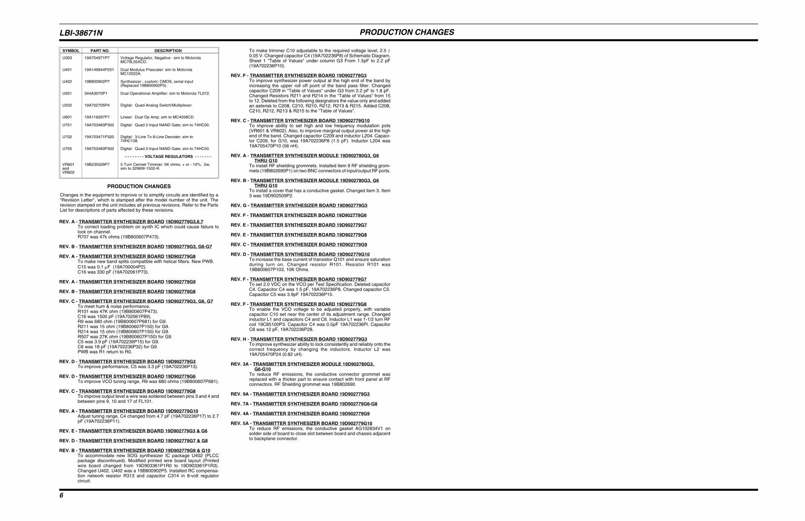
Changes in the equipment to improve or to simplify circuits are identified by a"Revision Letter", which is stamped after the model number of the unit. Therevision stamped on the unit includes all previous revisions. Refer to the PartsList for descriptions of parts affected by these revisions.
REV. A - TRANSMITTER SYNTHESIZER BOARD 19D902779G3,6,7To correct loading problem on synth IC which could cause failure tolock on channel. R707 was 47k ohms (19B800607P473).
REV. B - TRANSMITTER SYNTHESIZER BOARD 19D902779G3, G6-G7
REV. A - TRANSMITTER SYNTHESIZER BOARD 19D902779G8To make new band splits compatible with helical filters. New PWB.C15 was 0.1 µF (19A700004P2).C16 was 330 pF (19A702061P73).
REV. A - TRANSMITTER SYNTHESIZER BOARD 19D902779G9
REV. B - TRANSMITTER SYNTHESIZER BOARD 19D902779G8
REV. C - TRANSMITTER SYNTHESIZER BOARD 19D902779G3, G6, G7To meet hum & noise performance.R101 was 47K ohm (19B800607P473).C16 was 1500 pF (19A702061P89).R9 was 680 ohm (19B800607P681) for G9.R211 was 15 ohm (19B800607P150) for G9.R214 was 15 ohm (19B800607P150) for G9.R507 was 27K ohm (19B800607P150) for G9.C5 was 3.9 pF (19A702236P15) for G9.C6 was 18 pF (19A702236P32) for G9.PWB was R1 return to R0.
REV. D - TRANSMITTER SYNTHESIZER BOARD 19D902779G3To improve performance, C5 was 3.3 pF (19A702236P13).
REV. D - TRANSMITTER SYNTHESIZER BOARD 19D902779G6To improve VCO tuning range, R9 was 680 ohms (19B800607P681).
REV. C - TRANSMITTER SYNTHESIZER BOARD 19D902779G8To improve output level a wire was soldered between pins 3 and 4 andbetween pins 9, 10 and 17 of FL101.
REV. A - TRANSMITTER SYNTHESIZER BOARD 19D902779G10Adjust tuning range, C4 changed from 4.7 pF (19A702236P17) to 2.7pF (19A702236P11).
REV. E - TRANSMITTER SYNTHESIZER BOARD 19D902779G3 & G6
REV. D - TRANSMITTER SYNTHESIZER BOARD 19D902779G7 & G8
REV. B - TRANSMITTER SYNTHESIZER BOARD 19D902779G9 & G10To accommodate new SOG synthesizer IC package U402 (PLCCpackage discontinued). Modified printed wire board layout (Printedwire board changed from 19D903361P1R0 to 19D903361P1R3).Changed U402. U402 was a 19B800902P5. Installed RC compensa-tion network resistor R313 and capacitor C314 in 8-volt regulatorcircuit.
To make trimmer C10 adjustable to the required voltage level, 2.5 ±0.05 V. Changed capacitor C4 (19A702236P8) of Schematic Diagram,Sheet 1 "Table of Values" under column G3 From 1.5pF to 2.2 pF(19A702236P10).
REV. F - TRANSMITTER SYNTHESIZER BOARD 19D902779G3To improve synthesizer power output at the high end of the band byincreasing the upper roll off point of the band pass filter. Changedcapacitor C209 in "Table of Values" under G3 from 2.2 pF to 1.8 pF.Changed Resistors R211 and R214 in the "Table of Values" from 15to 12. Deleted from the following designators the value only and addedan asterisk to C208, C210, R210, R212, R213 & R215. Added C208,C210, R212, R213 & R215 to the "Table of Values".
REV. C - TRANSMITTER SYNTHESIZER BOARD 19D902779G10To improve ability to set high and low frequency modulation pots(VR601 & VR602). Also, to improve marginal output power at the highend of the band. Changed capacitor C209 and inductor L204. Capaci-tor C209, for G10, was 19A702236P8 (1.5 pF). Inductor L204 was19A705470P10 (56 nH).
REV. A - TRANSMITTER SYNTHESIZER MODULE 19D902780G3, G6THRU G10
To install RF shielding grommets. Installed item 9 RF shielding grom-mets (19B802690P1) on two BNC connectors of input/output RF ports.
REV. B - TRANSMITTER SYNTHESIZER MODULE 19D902780G3, G6THRU G10
To install a cover that has a conductive gasket. Changed item 3. Item3 was 19D902509P2.
REV. G - TRANSMITTER SYNTHESIZER BOARD 19D902779G3
REV. F - TRANSMITTER SYNTHESIZER BOARD 19D902779G6
REV. E - TRANSMITTER SYNTHESIZER BOARD 19D902779G7
REV. E - TRANSMITTER SYNTHESIZER BOARD 19D902779G8
REV. C - TRANSMITTER SYNTHESIZER BOARD 19D902779G9
REV. D - TRANSMITTER SYNTHESIZER BOARD 19D902779G10To increase the base current of transistor Q101 and ensure saturationduring turn on. Changed resistor R101. Resistor R101 was19B800607P103, 10K Ohms.
REV. F - TRANSMITTER SYNTHESIZER BOARD 19D902779G7To set 2.0 VDC on the VCO per Test Specification. Deleted capacitorC4. Capacitor C4 was 1.5 pF, 19A702236P8. Changed capacitor C5.Capacitor C5 was 3.9pF 19A702236P15.
REV. F - TRANSMITTER SYNTHESIZER BOARD 19D902779G8To enable the VCO voltage to be adjusted properly, with variablecapacitor C10 set near the center of its adjustment range. Changedinductor L1 and capacitors C4 and C6. Inductor L1 was 1-1/2 turn RFcoil 19C85100P3. Capacitor C4 was 0.5pF 19A702236Pl. CapacitorC6 was 12 pF, 19A702236P28.
REV. H - TRANSMITTER SYNTHESIZER BOARD 19D902779G3To improve synthesizer ability to lock consistently and reliably onto thecorrect frequency by changing the inductors. Inductor L2 was19A705470P24 (0.82 uH).
REV. 3A - TRANSMITTER SYNTHESIZER MODULE 19D902780G3, G6-G10
To reduce RF emissions, the conductive connector grommet wasreplaced with a thicker part to ensure contact with front panel at RFconnectors. RF Shielding grommet was 19B802690.
REV. 9A - TRANSMITTER SYNTHESIZER BOARD 19D902779G3
REV. 7A - TRANSMITTER SYNTHESIZER BOARD 19D902779G6-G8
REV. 4A - TRANSMITTER SYNTHESIZER BOARD 19D902779G9
REV. 5A - TRANSMITTER SYNTHESIZER BOARD 19D902779G10To reduce RF emissions, the conductive gasket AG102834V1 onsolder side of board to close slot between board and chassis adjacentto backplane connector.
LBI-38671N
6
IC DATA
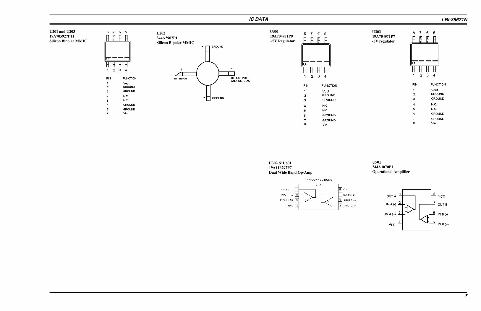
U30119A704971P9+5V Regulator
U302 & U60119A116297P7Dual Wide Band Op-Amp
U202344A3907P1Silicon Bipolar MMIC
U30319A704971P7-5V regulator
U501344A3070P1Operational Amplifier
U201 and U20319A705927P11Silicon Bipolar MMIC
LBI-38671N
7
IC DATA
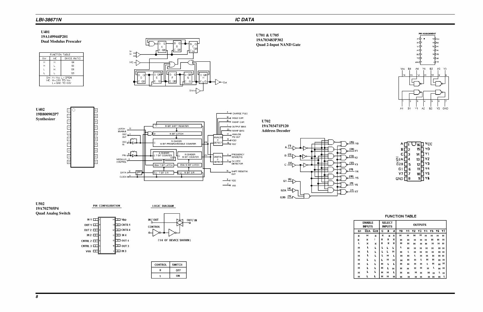
U40119A149944P201Dual Modulus Prescaler
1 20
3
2
4
5
6
7
8
10 11
12
13
14
15
16
17
18
19
9
U40219B800902P7Synthesizer
U50219A702705P4Quad Analog Switch
U701 & U70519A703483P302Quad 2-Input NAND Gate
U70219A703471P120Address Decoder
LBI-38671N
8
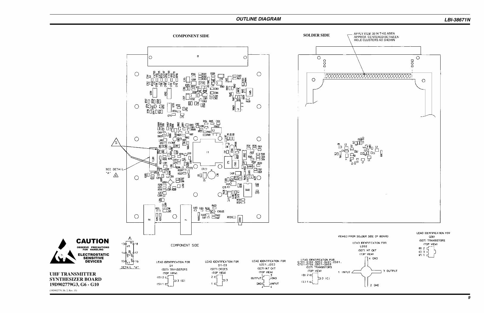
OUTLINE DIAGRAM
UHF TRANSMITTERSYNTHESIZER BOARD19D902779G3, G6 - G10(19D902779, Sh. 2, Rev. 15)
COMPONENT SIDE SOLDER SIDE
LBI-38671N
9
SCHEMATIC DIAGRAM
UHF TRANSMITTER SYNTHESIZER19D902780G3, G6 - G10(19D903363, Sh. 1, Rev. 22)
LBI-38671N
10
SCHEMATIC DIAGRAM
UHF TRANSMITTER SYNTHESIZER19D902780G3, G6 - G10
(19D903363, Sh. 2, Rev. 22)
LBI-38671N
11
SCHEMATIC DIAGRAM
UHF TRANSMITTER SYNTHESIZER19D902780G3, G6 - G10(19D903363, Sh. 3, Rev. 22)
LBI-38671N
12
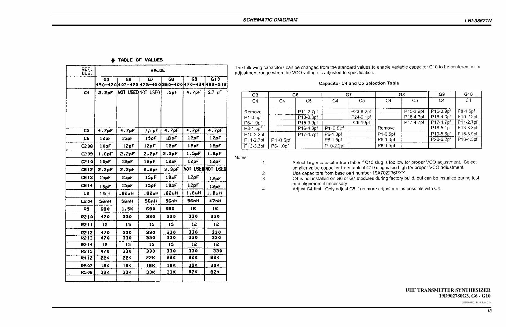
SCHEMATIC DIAGRAM
UHF TRANSMITTER SYNTHESIZER19D902780G3, G6 - G10
(19D903363, Sh. 4, Rev. 22)
LBI-38671N
13