Embed Size (px)
Citation preview

LBI-38275F
DESCRIPTION
The PCS Por tab le Rad io Rear Assembl ies19D902175G1 and G2 provide metal housings for RFBoards 19D438222G1 (136-153 MHz) and 19D438222G3(150-174) respectively. The RF boards are the same exceptfor certain frequency sensitive elements.
The RF boards consist of the following circuits:
• A frequency synthesizer for generating the transmitcarrier frequency and the receive circuit first mixerinjection frequency.
• The transmit circuit, receive circuit and TX/RXswitch.
• A voltage regulator and low battery switch.
Refer to Figure 1 for a block diagram of the synthesizercircuit. Refer to Figure 2 for a transmit and receive circuitblock diagram. Transmit circuit adjustments for frequencyand power are accessible from the top side of the board, asare IF alignment, second oscillator and quadrature detectoradjustments for the receiver circuit. Chip components onthe bottom of the board provide optimum RF performance.
Selected use of sealed modules permits small board sizeas well as RF and mechanical protection for sensitive cir-cuitry. Modules are NOT repairable and must be replacedif they are determined to be damaged. A single friction fitshield provides RF shielding.
MAINTENANCE MANUALPCS REAR ASSEMBLIES
19D902175G1 (136-153 MHz)19D902175G2 (150-174 MHz)
TABLE OF CONTENTS
Page
DESCRIPTION . . . . . . . . . . . . . . . . . . . . . . . . . . . . . . . . . . . . . . . . . . . Front Cover
CIRCUIT ANALYSIS . . . . . . . . . . . . . . . . . . . . . . . . . . . . . . . . . . . . . . . . 1Synthesizer Circuit . . . . . . . . . . . . . . . . . . . . . . . . . . . . . . . . . . . . . . . 1Transmitter Circuit . . . . . . . . . . . . . . . . . . . . . . . . . . . . . . . . . . . . . . . 1Receiver Circuit . . . . . . . . . . . . . . . . . . . . . . . . . . . . . . . . . . . . . . . . . 1
BLOCK DIAGRAM . . . . . . . . . . . . . . . . . . . . . . . . . . . . . . . . . . . . . . . . . 2
OUTLINE DIAGRAM . . . . . . . . . . . . . . . . . . . . . . . . . . . . . . . . . . . . . . . . 3
SCHEMATIC DIAGRAM . . . . . . . . . . . . . . . . . . . . . . . . . . . . . . . . . . . . . . 5
PARTS LIST . . . . . . . . . . . . . . . . . . . . . . . . . . . . . . . . . . . . . . . . . . . . . 8
PRODUCTION CHANGES . . . . . . . . . . . . . . . . . . . . . . . . . . . . . . . . . . . . . 10
IC DATA . . . . . . . . . . . . . . . . . . . . . . . . . . . . . . . . . . . . . . . . . . . . . . . 10
ericssonz
Ericsson Inc.Private Radio SystemsMountain View RoadLynchburg, Virginia 245021-800-528-7711 (Outside USA, 804-528-7711) Printed in U.S.A.

CIRCUIT ANALYSIS
SYNTHESIZER CIRCUIT
The frequency synthesizer circuit generates all transmitand receive RF frequencies for the PCS Personal Radio. Thiscircuit uses a phase-locked Voltage Controlled Oscillator(VCO) operating on the actual transmitter frequency (136-153or 150-174 MHz) during transmit and 45 MHz above theactual receive frequency during receive. The synthesizer out-put signal is generated directly by VCO module U204 and fedthrough a low pass filter to a LO buffer, a PA buffer and aprescaler buffer.
The synthesizer frequency output is controlled by a micro-processor on the Audio Logic Board. Frequency stability ismaintained by a temperature compensated crystal controlledoscillator (TCXO) module. The oscillator has a stability of 5PPM over the temperature range of -30C to 60C and deter-mines the overall frequency stability of the radio.
The VCO output is also buffered by transistor Q201 to feeddivide by 64/65 dual modulus prescaler U205. The prescalerfeeds the Fin input of Phase-Lock-Loop (PLL) chip U201.Within U201, the prescaler signal is further divided down to5 KHz to be compared with a reference signal. This referencesignal is derived from 12.8 MHz TCXO module U203. ThePLL chip, U201, divides the 12.8 MHz TCXO down to the 5KHz reference frequency. Divider circuits in U201 are pro-grammed by three inputs from the Audio/Logic Board. Theseare SYN ENABLE, SYN DATA and SYC CLOCK lines. ALOCK DETECT line from the PLL chip to the audio boardmicroprocessor for processing to prevent transmissions whenthe synthesizer is unlocked. A blinking BAT flag is displayedon the LCD and a pulsed beep will be sounded if this conditionoccurs.
Audio modulation from the Audio/Logic Board is appliedto loop filter circuit board A201 in the synthesizer circuit. Theaudio is summed with the unfiltered control voltage and fedto operational amplifier U1 on the loop filter Board. AmplifierU1 is biased to produce gain variation with different controlvoltages. When the control voltage is below 1.7 volts, bothdiodes in diode package D1 are biased off. The operationalamplifier gain is then one. As the control voltage rises aboveapproximately 1.7 volts, one of the diodes (D1) is forwardbiased. This increases the operational amplifier gain to ap-proximately 1.2. Further increases in the control voltageabove approximately 2.5 volts turns both diode paths on, thusincreasing the gain to about 1.4. Gain variation verses controlvoltage compensates for decreasing VCO gain and keeps theVCO gain constant at higher control voltages. The net effectof this is to linearize the loop response across the frequency
band to maintain relatively constant audio modulation andconstant digital Channel Guard waveshape.
The synthesizer enable line also drives bilateral switchesU2A and U2B on the loop filter board. The pulse applied tothese gates, when channel changes occur, turns the gates onwhich shorts out resistors R11 and R12. This allows rapidchannel acquisition.
At low control voltages, below approximately 0.9 volts,operational amplifier U1B is enabled by the pulse on thesynthesizer enable line. This enables transistor Q1 for theduration of the channel change pulse. Transistor Q1 acts as acurrent sink for operational amplifier U1A which speeds upthe slow rate on U1A at low voltages.
TRANSMIT CIRCUIT
The transmit circuit consists of a transmit buffer amplifier,a 7-watt power amplifier (U101), a Power Control circuit(A101), a low pass filter circuit and a Tx/Rx switch. Transis-tors Q102 through Q105 switch power to the TX stages anddrives the Disable Line of the Power Control Module.
Tx Buffer
Transmit buffer transistor Q101 is driven by the synthe-sizer VCO output at a level of approximately 0 dBm. Ampli-fier transistor Q101, in turn, drives power module U101 atapproximately +3 dBm. DC power is applied to the buffer onlyin the transmit mode and is regulated to provide constant drivewith decreasing battery voltage.
Power Module
Power module U101 is a three-stage broadband poweramplifier with internal matching. This module mounts to therear casting for heat sinking. Output power is controlled byvarying the supply voltage to stage two of the module. Stageone and bias for stage two are supplied with the same regu-lated voltage as the transmit buffer. The final PA stage issupplied by the battery voltage in order to obtain maximumpower. The final stage power feed is through inductor L103.The d.c. voltage drop across this coil provides the sensevoltage for power control.
Power Control Board
The power control circuitry, located on circuit boardA101, has the task of sensing the d.c. drop across L103 andproducing an output d.c. voltage to control stage two of thePA module. This feedback system holds the current to stagethree of the PA module essentially constant as frequency,battery voltage, temperature and load varies. The outputcurrent level and output power are set by power adjustingpotentiometer R119, located on the RF Board. A lowerpower level may be set by adjusting potentiometer R11,located on the Power Control Board. Transistor Q2 on thepower control board must be turned ON to enable the R11path. This transistor is in turn controlled by the microproc-essor on the Audio/Logic Board to control high or lowpower operation.
The input voltages to the power control module are onPins 7 and 8. These voltages are divided down by precisionresistors to set input voltages to operational amplifier U1.The voltage on the positive terminal of U1 may be adjustedabove and below the divider voltage on the negative termi-nal of U1. When the positive and negative terminals are atequal potentials, the output of U1 is about 5 volts (depend-ing on battery voltage). As the voltage on the positiveterminal is adjusted by potentiometer R11, the output of U1moves higher or lower in potential by about 60 time the ^Vin. This output is buffered by emitter follower transistorQ3. The output voltage on Pin 2 is set by the resistor ratioR7+R8/R7. Current is supplied at this output mode byexternal transistor Q106.
Low Pass Filter
A six element low pass filter is provided to preventexcessive transmitter harmonics from being transmitted.This filter in conjunction with the matching circuitry in thePA module limits the conducted harmonic energy to lessthan -30 dBm.
Tx/Rx Switch
The Tx/Rx Switch consists of series PIN diode D101and shunt PIN diode D102. Both diodes are off duringreceive and are therefore essentially open. This isolates thetransmit circuit from the receive circuit while in the receivemode. During transmit, regulated voltage is switched toinductor L105. This produces a d.c. current through bothD101 and D102, which transforms both diodes into RFshorts. This allows the PA output power to be conducted tothe radio antenna. The RF short produced by D102 protects
the receiver but is still essentially an open to the transmitter.This is true because inductor L106 and part of capacitorC116 form a parallel resonant circuit across the transmitoutput.
Tx Switches
The transmit circuit is enabled by the DPTT line fromthe Audio/Logic Board. When the PTT button is activated,the DPTT line is pulled high. This turns transistor Q102 onand allows transistors Q103, Q104 and Q105 to conduct.The voltage on the emitter of transistor Q104 is approxi-mately 0.7 volts (VBE + VSAT) below the regulated 5.4Volts. The voltage at the collector of transistor Q105 is setby the (R117 + R118)/R117 resistor ratio. This boosts theoutput voltage back to about 5.4 volts while allowing Q105to supply the relatively high currents needed for the TxBuffer, the PA module and the PIN diode switch.
The collector of transistor Q102 is also used to drivetransmit disable transistor Q1 located on the power controlmodule. When in the Rx state, the base of Q1 is baised onby a high voltage level at the collector of Q102. This in turnkeeps the positive terminal of U1 sufficiently low to drivethe output of U1 low enough to bias Q3 off. When Q102 isturned on by the DPTT line, transistor Q1 is biased off. Thisallows the normal Tx operation previously described.
RECEIVE CIRCUIT
The dual conversion receive circuit consists of a re-ceiver front end, a 45 MHz first IF and a 455 kHz secondIF with an FM detector. All audio processing and squelchfunctions are accomplished on the Audio/Logic Board.
Front End
RF is coupled from antenna jack J1 to the RF Boardthrough antenna clip connector J101. The receive signal isthen conducted through the Tx low pass filter to receivepreselector filter Z401. This is a fixed tuned 3-pole bandpass filter covering the 136 to 153 or 150 to 174 MHz bands.Its output is matched to the input of RF amplifier transistorQ401. A fixed tuned 2-pole output filter is connected be-tween the RF amplifier and double balanced mixer Z402.About 10 dB of RF gain is provided to the mixer input. TheLocal Oscillator (LO) port of the mixer (Pin 1) is driven byLO buffer transistor Q450. The filtered synthesizer outputdrives this buffer. The output of Q450 drives a 2-pole filterwhich couples the drive to the mixer at about +4 dBm.
Copyright © April, 1989, General Electric Company
REAR
ASSEMBLY
LBI-38275 LBI-38275
1

45 MHz IF
The mixer output is connected to the Source of commonGate Field Effect Transistor (FET) Q501. This stage pro-vides a low impedance input to match the mixer and a highimpedance output to drive the 45 MHz 4-pole crystal filter.The crystal filter output is amplified by bipolar devicetransistor Q502. This IF amplifier output drives the SecondMixer circuit in Mixer/Limiter/FM Detector module U501.Crystal Y101 is an external crystal operating a 45.455 MHz.This crystal when coupled to the internal circuitry forms thesecond LO for the second mixer circuit. The frequency ofthe second LO is adjusted with inductor L505. The secondmixer output is a 455 kHz IF and is filtered by a 4-poleceramic filter. This output is further amplified and limitedby U501. A quadrature detector circuit provides an audiooutput from U501. The quadrature detector coil is L506.The audio output is pre-filtered and connected to theAudio/Logic Board as VOL SQ HI.
5.4 Volt Regulator
The 5.4 volt regulator circuit supplies a regulated 5.4volts to all circuits requiring a stable reference voltage. Thisregulated voltage is generated by voltage reference diodeU801 and transistors Q801, Q802 and Q803. Diode U801provides 2.5 volts which is stable with both temperature and
battery voltage. The 2.5 volt reference is fed to the base ofQ802. Transistors Q802 and Q803 form a differential am-plifier while Q801 acts as a pass transistor. The regulated5.4 volts output on the collector of Q801 is divided byvoltage divider resistors R805 and R806 to apply 2.5 voltsto the base of transistor Q803. With this voltage on the baseof Q803 the differential amplifier is balanced.
Battery Indicator
Transistor Q804 senses the battery voltage and com-pares it to the regulated 5.4 volts on the emitter. When thebattery voltage drops to approximately 6.3 volts, Q804 issufficiently on to produce about 0.4 volts on the batteryindicator output (P801-1). This voltage is fed to theaudio/logic board to drive an inverter which toggles a mi-croprocessor port to provide a low battery indication.
Another effect at low battery voltage is produced by thevoltage on the collector of Q804 driving Pin 6 of powercontrol module U1. A slight increase of this voltage on thenegative terminal of U1 causes the output of U1 to drop andthe control voltage to be reduced. The final result is a slightdrop in RF power output. Consequently, as the end ofbattery is approached, the RF power is throttled back. Thisgives the user additional transmit time before total loss ofpower due to low battery.
BLOCK DIAGRAM
Figure 1 - Synthesizer Circuit
Fig
ure
2 -
Tra
nsm
it A
nd R
ecei
ve C
ircu
it
LBI-38275 LBI-38275
2

OUTLINE DIAGRAM
POWER CONTROL BOARD A101
19B801519G1
(19B801519, Sh. 1, Rev. 3)(19C851653, Component Side, Rev. 4)
(19C851653, Solder Side, Rev. 4)
LOOP FILTER BOARD A201
19C851646G1
(19C851646, Sh. 1, Rev. 2)(19C851647, Component Side, Rev. 3)
(19C851647, Solder Side, Rev. 3)
COMPONENT SIDE SOLDER SIDE COMPONENT SIDE SOLDER SIDE
REAR
ASSEMBLY
LBI-38275 LBI-38275
3

RF BOARDS19D438222G1 & G3
OUTLINE DIAGRAM
(19D438222, Sh.3, Rev. 3)(19D902627, First Layer, Rev. 4)
(19D902627, Fourth Layer, Rev. 4)
(19D438222, Sh. 4, Rev. 5)(19D902627, Fourth Layer, Rev. 4)
COMPONENT SIDESOLDER SIDE
LBI-38275 LBI-38275
4

SCHEMATIC DIAGRAM
RF BOARDS19D438222G1 & G3
(19D902715, Sh. 1, Rev. 5A)
REAR
ASSEMBLY
LBI-38275 LBI-38275
5

SCHEMATIC DIAGRAM
RF BOARDS19D438222G1 & G3(19D902715, Sh. 2, Rev. 5A)
LBI-38275 LBI-38275
6
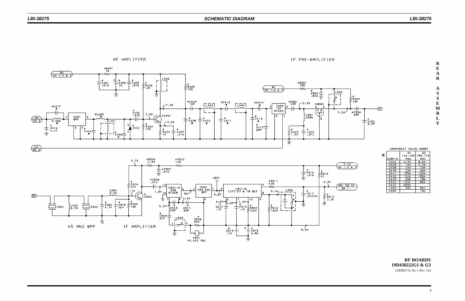
SCHEMATIC DIAGRAM
RF BOARDS19D438222G1 & G3
(19D902715, Sh. 3, Rev. 5A)
REAR
ASSEMBLY
LBI-38275 LBI-38275
7

RADIO REAR ASSEMBLY19D901275G1 (136-153 MHz)19D902175G2 (150-174 MHz)
ISSUE 7
PARTS LIST
SYMBOL PART NUMBER DESCRIPTION
A1 RF BOARD19D438222G1 (136-153 MHz)19D438222G3 (150-174 MHz)
A101 POWER CONTROL MODULE19B801519G1
— — — — CAPACITORS — — — — —
C1 19A702061P69 Ceramic: 220 pF ±5%, 50 VDCW, temp coef 0 ±30 PPM.
C2 19A702061P61 Ceramic: 100 pF ±5%, 50 VDCW, temp coef 0 ±30 PPM.
C3 19A702061P69 Ceramic: 220 pF ±5%, 50 VDCW, temp coef 0 ±30 PPM.
C4 19A702052P28 Ceramic: 0.022 uF ±10%, 50 VDCW.
C5 19A702061P69 Ceramic: 220 pF ±5%, 50 VDCW, temp coef 0 ±30 PPM.
— — — — TRANSISTORS — — — — —
Q1 19A700076P2 Silicon, NPN: sim to MMBT3904, low profilethruQ3
— — — — RESISTORS — — — — —
R1 19A702931P308 Metal film: 11.8K ohms ±1%, 200 VDCW, 1/8 w.
R2 19A702931P334 Metal film: 22.1K ohms ±1%, 200 VDCW, 1/8 w.
R3 19B801251P102 Metal film: 1K ohms ±5%, 1/10 w.
R4 19A702931P335 Metal film: 22.6K ohms ±1%, 200 VDCW, 1/8 w.
R5 19A702931P358 Metal film: 39.2K ohms ±1%, 200 VDCW, 1/8 w.
R6 19B801251P225 Metal film: 2.2M ohms ±5%, 1/10 w.
R7 19B801251P221 Metal film: 220 ohms ±5%, 1/10 w.
R8 19B801251P471 Metal film: 470 ohms ±5%, 1/10 w.
R9 19A702931P281 Metal film: 6810 ohms ±1%, 200 VDCW, 1/8 w.
R10 19B801251P123 Metal film: 12K ohms ±5%, 1/10 w.
R11 19A705496P8 Variable: 200K ohms max, 1/10 w.
R12 19B801251P473 Metal film: 47K ohms ±5%, 1/10 w.andR13
— — INTEGRATED CIRCUITS — — —
U1 19A702293P3 Linear: Dual Op Amp; sim to LM358D.
A201 LOOP FILTER MODULE19C851974G1
— — — — CAPACITORS — — — — —
*C1 19A702052P12 Ceramic: 0.0068 uF ±5%, 50 VDCW.
C2 19A702061P77 Ceramic: 470 pF 5±%, 50 VDCW, temp coef 0and ±30 PPM.C3
C4 19A702061P29 Ceramic: 22 pF ±5%, 50 VDCW, temp coef 0±30 PPM.
C5 19A702052P30 Ceramic: 0.022 uF ±10%, 50 VDCW.
— — — — — DIODES — — — — — —
D1 19A703561P2 Silicon, fast recovery (2 diodes in series).
— — — — TRANSISTORS — — — — —
Q1 19A700076P2 Silicon, NPN: sim to MMBT3904, low profile.
— — — — RESISTORS — — — — —
*R1 REP624656/16 Metal film: 160K ohms ± 1%, 1/10 ω.
R2 19B801251P124 Metal film: 120K ohms ±5%, 1/10 w.
R3 19B801251P104 Metal film: 100K ohms ±5%, 1/10 w.
R4 19B801251P682 Metal film: 6.8K ohms ±5%, 1/10 w.
R5 19A702931P377 Metal film: 61.9K ohms ±1%, 200 VDCW, 1/8 w
R6 19B801251P393 Metal film: 39K ohms ±5%, 1/10 w.
R7 19B801251P104 Metal film: 100K ohms ±5%, 1/10 w.
* COMPONENTS, ADDED, DELETED OR CHANGED BY PRODUCTION CHANGES
SYMBOL PART NUMBER DESCRIPTION
R9 19B801251P104 Metal film: 100K ohms ±5%, 1/10 w.andR10
R11 19B801251P105 Metal film: 1M ohms ±5%, 1/10 w.
R12 19B801251P333 Metal film: 33K ohms ±5%, 1/10 w.
R13 19B801251P224 Metal film: 220K ohms ±5%, 1/10 w.R14 19B801251P104 Metal film: 100K ohms ±5%, 1/10 w.
— — INTEGRATED CIRCUITS — — — —
U1 19A702293P3 Linear: Dual Op Amp; sim to LM358D.
U2 19A702705P4 Digital: uad Analog Switch/Multiplexer; sim to4066BM.
TRANSMITTER
— — — — CAPACITORS — — — — — —
C101 19A702061P77 Ceramic: 470 pF ±5%, 50 VDCW, temp coef 0thru ±30 PPM.C104
C105 19A705205P2 Tantalum: 1 uF, 16 VDCW; sim to Sprague and 293D.C106
C107 19A702061P77 Ceramic: 470 pF ±5%, 50 VDCW, temp coef 0±30 PPM.
C109 19A705205P2 Tantalum: 1 uF, 16 VDCW; sim to Sprague 293D.
C110 19A702061P77 Ceramic: 470 pF ±5%, 50 VDCW, temp coef 0±30 PPM..
C111 19A702061P77 Ceramic: 470 pF ±5%, 50 VDCW, temp coef 0±30 PPM.
C112 19A702061P33 Ceramic: 27 pF ±5%, 50 VDCW, temp coef 0±30 PPM. (Used in G3).
C112 19A702236P40 Ceramic: 39 pF ±5%, 50 VDCW, temp coef 0±30 PPM. (Used in G1).
C113 19A702061P77 Ceramic: 470 pF ±5%, 50 VDCW, temp coef 0±30 PPM.
C114 19A702061P21 Ceramic: 15 pF ±5%, 50 VDCW, temp coef 0±30 PPM. (Used in G1).
C114 19A702061P17 Ceramic: 12 pF ±5%, 50 VDCW, temp coef 0±30 PPM. (Used in G3).
C115 19A702061P77 Ceramic: 470 pF ±5%, 50 VDCW, temp coef 0±30 PPM.
C116 19A702061P33 Ceramic: 27 pF ±5%, 50 VDCW, temp coef 0±30 PPM. (Used in G1).
C116 19A702061P29 Ceramic: 22 pF ±5%, 50 VDCW, temp coef 0±30 PPM. (Used in G3).
C117 19A702061P17 Ceramic: 12 pF ±5%, 50 VDCW, temp coef 0±30 PPM. (Used in G1).
C117 19A702061P13 Ceramic: 10 pF ±5%, 50 VDCW, temp coef 0±30 PPM. (Used in G3).
C118 19A702061P25 Ceramic: 18 pF ±5%, 50 VDCW, temp coef 0±30 PPM. (Used in G1).
C118 19A702061P21 Ceramic: 15 pF ±5%, 50 VDCW, temp coef 0±30 PPM. (Used in G3).
C119 19A702052P5 Ceramic: 1000 pF ±10%, 50 VDCW.thruC121
C122 19A702052P14 Ceramic: 0.01 uF ±10%, 50 VDCW.
— — — — — DIODES — — — — — — —
D101 19A700155P2 Silicon: fwd current 100 mA, 35 PIV.andD102
— — — — — JACKS — — — — — — —
J101 19B801491P2 Clip, Antenna.
— — — — INDUCTORS — — — — — —
L101 19A700024P13 Coil, RF: 1.0 uH ±10%.andL102
L103 19B801566P11 Shield.
L104 19A705470P15 Coil, 150 nH ±20% (Used in G3).
SYMBOL PART NUMBER DESCRIPTION
C213 19A702061P77 Ceramic: 470 pF ±5%, 50 VDCW, temp coef 0±30 PPM.
*C214 T644ACP333K Polyester: 0.033 uF ±10%, 50 VDCW.
C215 19A700004P10 Metallized Polyester: 1.0 uF ±10%, 63 VDCW.
C216 19A702052P14 Ceramic: 0.01 uF ±10%, 50 VDCW.
C217 19A702061P13 Ceramic: 10 pF ±5%, 50 VDCW, temp coef 0±30 PPM.
C218 19A702061P12 Ceramic: 8.2 pF ±0.5 pF, 50 VDCW, tempcoef 0 ±60 PPM.
C220 19A705202P2 Tantalum: 1 uF, 16 VDCW; sim to Sprague 293D. (Used in G3).
— — — — TRANSISTOR — — — — — —
Q201 19A704708P2 Silicon, NPN: sim to NEC 2SC3356.
— — — — RESISTORS — — — — — —
R201 19B801251P104 Metal film: 100K ohms ±5%, 1/10 w.
R202 19B801251P224 Metal film: 220K ohms ±5%, 1/10 w.
R203 19A702931P233 Metal film: 2150 ohms ±1%, 200 VDCW, 1/8 w.
R204 19B801251P272 Metal film: 2.7K ohms ±5%, 1/10 w.
R205 19B801251P100 Metal film: 10 ohms ±5%, 1/10 w.
R206 19B801251P331 Metal film: 330 ohms ±5%, 1/10 w.
R207 19B801251P103 Metal film: 10K ohms ±5%, 1/10 w.andR208
R209 19B801251P102 Metal film: 1K ohms ±5%, 1/10 w.
R210 19B801251P470 Metal film: 47 ohms ±5%, 1/10 w.
R211 19B801251P103 Metal film: 10K ohms ±5%, 1/10 w.
R212 19B801251P470 Metal film: 47 ohms ±5%, 1/10 w.
R213 19B801251P2R2 Metal film: 2.2 ohms ±5%, 1/10 w.
— — INTEGRATED CIRCUITS — — — —
U201 19B800902P1 Synthesizer: CMOS, Serial Programming; sim toMC145159P.
U202 19A703091P1 Digital: /64, /65 Prescaler; sim to MC12017P.
U203 19B801351P8 Reference Oscillator.
U204 19A705628P1 Voltage Controlled Oscillator (Used in G1).
U204 19C851913G2 Voltage Controlled Oscillator (Used in G3).
— — — — — CABLES — — — — — — —
W201 Part of printed wire board.andW202
RECEIVER
— — — — CAPACITORS — — — — — —
C401 19A702052P14 Ceramic: 0.01 uF ±10%, 50 VDCW.
C402 19A705205P2 Tantalum: 1 uF, 16 VDCW; sim to Sprague 293D.
C403 19A702052P14 Ceramic: 0.01 uF ±10%, 50 VDCW.
C404 19A702236P15 Ceramic: 3.9 pF ±.25 pF, 50 VDCW, tempcoef 0 ±30 PPM. (Used in G1).
C404 19A702061P12 Ceramic: 8.2 pF ±0.5 pF, 50 VDCW, tempcoef 0 ±60 PPM. (Used in G3).
C405 19A702061P13 Ceramic: 10 pF ±5%, 50 VDCW, temp coef 0±30 PPM. (Used in G1).
C405 19A702061P9 Ceramic: 4.7 pF ±0.5 pF, 50 VDCW, tempcoef 0 ±60 PPM. (Used in G3).
C406 19A702052P14 Ceramic: 0.01 uF ±10%, 50 VDCW.andC407
C408 19A702061P21 Ceramic: 15 pF ±5%, 50 VDCW, temp coef 0±30 PPM. (Used in G1).
C408 19A702061P13 Ceramic: 10 pF ±5%, 50 VDCW, temp coef 0±30 PPM. (Used in G3).
C409 19A702061P13 Ceramic: 10 pF ±5%, 50 VDCW, temp coef 0±30 PPM.
C410 19A702061P37 Ceramic: 33 pF ±5%, 50 VDCW, temp coef 0±30 PPM. (Used in G1).
SYMBOL PART NUMBER DESCRIPTION
L104 19A705470P10 Coil, 56 nH ±20%. (Used in G3).
L105 19A700024P13 Coil, RF: 1.0 uH ±10%.
L106 19B800891P4 Coil, F Choke: sim to Paul Smith SK-890-1.
L107 19B800891P3 Coil, RF Choke; sim to Paul Smith SK890-1.
— — — TRANSISTORS — — — — —
Q101 19A704708P2 Silicon, NPN: sim to NEC 2SC3356.
Q102 19A700076P2 Silicon, NPN: sim to MMBT3904, low profile.
103 19A700059P2 Silicon, PNP: sim to MMBT3906, low profile.
Q104 19A700076P2 Silicon, NPN: sim to MMBT3904, low profile.
Q105 19A704972P1 Silicon, PNP: sim to Motorola 2N4918.and106
— — — — RESISTOR — — — — — —
R101 19B801251P101 Metal film: 100 ohms ±5%, 1/10 w.
R102 19B801251P681 Metal film: 680 ohms ±5%, 1/10 w.
R103 19B801251P680 Metal film: 68 ohms ±5%, 1/10 w.
R104 19B801251P330 Metal film: 33 ohms ±5%, 1/10 w.
R105 19B801251P332 Metal film: 3.3K ohms ±5%, 1/10 w.
R106 19B801251P331 Metal film: 330 ohms ±5%, 1/10 w.
R107 19B801251P271 Metal film: 270 ohms ±5%, 1/10 w.andR108
R109 19B801251P473 Metal film: 47K ohms ±5%, 1/10 w.
R110 19B801251P223 Metal film: 22K ohms ±5%, 1/10 w.
R111 19B801251P183 Metal film: 18K ohms ±5%, 1/10 w.
R112 19B801251P473 Metal film: 47K ohms ±5%, 1/10 w.
R113 19B801251P104 Metal film: 100K ohms ±5%, 1/10 w.andR114
R115 19B801251P102 Metal film: 1K ohms ±5%, 1/10 w.andR116
R117 19B801251P471 Metal film: 470 ohms ±5%, 1/10 w.
R118 19B801251P221 Metal film: 220 ohms ±5%, 1/10 w.
R119 19B800779P7 Variable: 3.3K ohms ±25%, 100 VDCW, .3 w.
R120 19B801251P184 Metal film: 180K ohms ±5%, 1/10 w.
R121 19B801251P151 Metal film: 150 ohms ±5%, 1/10 w.
— — INTEGRATED CIRCUITS — — —
U101 19A705774P1 Module: 136-155 MHz RF PA; sim to SHW1030.(Used in G1).
U101 19A705774P2 Module: 146-174 MHz RF PA; sim to SHW1031.(Used in G3).
— — — — — CABLES — — — — — —
W101 Part of printed wire board.
SYNTHESIZER
— — — — CAPACITORS — — — — —
C201 19A702061P69 Ceramic: 220 pF ±5%, 50 VDCW, temp coef 0±30 PPM.
C202 19A702052P5 Ceramic: 1000 pF ±10%, 50 VDCW.andC203
C204 19A702061P61 Ceramic: 100 pF ±5%, 50 VDCW, temp coef 0±30 PPM.
C205 19A702052P5 Ceramic: 1000 pF ±10%, 50 VDCW.
C207 19A702052P14 Ceramic: 0.01 uF ±10%, 50 VDCW.
C208 19A702052P5 Ceramic: 1000 pF ±10%, 50 VDCW.andC209
C210 19A702061P61 Ceramic: 100 pF ±5%, 50 VDCW, temp coef 0±30 PPM.
C211 19A702061P69 Ceramic: 220 pF ±5%, 50 VDCW, temp coef 0±30 PPM.
C212 19A702061P7 Ceramic: 3.3 pF ±0.5 pF, 50 VDCW, tempcoef 0 ±120 PPM.
LBI-38275 LBI-38275
8

PARTS LIST
SYMBOL PART NUMBER DESCRIPTION
C410 19A702061P29 Ceramic: 22 pF ±5%, 50 VDCW, temp coef 0±30 PPM. (Used in G3).
C411 19A702061P65 Ceramic: 150 pF ±5%, 50 VDCW, temp coef 0±30 PPM/xC. (Used in G1).
C411 19A702061P63 Ceramic: 120 pF ±5%, 50 VDCW, temp coef 0±30 PPM. (Used in G3).
C412 19A702061P65 Ceramic: 150 pF ±5%, 50 VDCW, temp coef 0±30 PPM/xC. (Used in G1).
C412 19A702061P63 Ceramic: 120 pF ±5%, 50 VDCW, temp coef 0±30 PPM. (Used in G3).
C413 19A702061P29 Ceramic: 22 pF ±5%, 50 VDCW, temp coef 0±30 PPM. (Used in G1).
C413 19A702061P21 Ceramic: 15 pF ±5%, 50 VDCW, temp coef 0±30 PPM. (Used in G3).
C414 19A702061P65 Ceramic: 150 pF ±5%, 50 VDCW, temp coef 0±30 PPM. (Used in G1).
C414 19A702061P57 Ceramic: 82 pF ±5%, 50 VDCW, temp coef 0±30 PPM. (Used in G3).
C415 19A702061P29 Ceramic: 22 pF ±5%, 50 VDCW, temp coef 0±30 PPM.
C416 19A702061P9 Ceramic: 4.7 pF ±0.5 pF, 50 VDCW, tempcoef 0 ±60 PPM.
C417 19A702061P69 Ceramic: 220 pF ±5%, 50 VDCW, temp coef 0±30 PPM. (Used in G1).
C450 19A704879P5 Electrolytic: 10 uF ±20%, 16 VDCW.
C451 19A702052P14 Ceramic: 0.01 uF ±10%, 50 VDCW.thruC453
C454 19A702061P13 Ceramic: 10 pF ±5%, 50 VDCW, temp coef 0±30 PPM. (Used in G1).
C454 19A702061P11 Ceramic: 6.8 pF ±0.5 pF, 50 VDCW, tempcoef 0 ±60 PPM. (Used in G3).
C455 19A702061P12 Ceramic: 8.2 pF ±0.5 pF, 50 VDCW, tempcoef 0 ±60 PPM.
C456 19A702061P41 Ceramic: 39 pF ±5%, 50 VDCW, temp coef 0±30 PPM. (Used in G1).
C456 19A702061P37 Ceramic: 33 pF ±5%, 50 VDCW, temp coef 0±30 PPM. (Used in G3).
C457 19A702061P29 Ceramic: 22 pF ±5%, 50 VDCW, temp coef 0±30 PPM. (Used in G1).
C457 19A702061P25 Ceramic: 18 pF ±5%, 50 VDCW, temp coef 0±30 PPM/xC. (Used in G3).
C458 19A702061P57 Ceramic: 82 pF ±5%, 50 VDCW, temp coef 0±30 PPM. (Used in G1).
C458 19A702061P45 Ceramic: 47 pF ±5%, 50 VDCW, temp coef 0±30 PPM. (Used in G3).
C459 19A702061P13 Ceramic: 10 pF ±5%, 50 VDCW, temp coef 0±30 PPM. (Used in G1).
C459 19A702061P9 Ceramic: 4.7 pF ±0.5 pF, 50 VDCW, tempcoef 0 ±60 PPM. (Used in G3).
— — — — — DIODES — — — — — —
D401 19A700155P2 Silicon, fwd current: 100 mA, 35 VIP.
— — — — INDUCTORS— — — — — —
L401 19B801493P6 Coil, RF; sim to Toko NE545GNAS-1130.
L402 19B801493P3 Coil, RF; sim to Toko NE545GNAS-100127.thruL404
L405 19A705470P11 Coil, Fixed: 68 nH; sim to Toko 380NB-68nM.(Used in G1).
L405 19A705470P12 Coil, Fixed: 82 nH; sim to Toko 380NB-82nM.(Used in G3).
L406 19A705470P3 Coil, Fixed: 15 nH; sim to Toko 380NB-15nM.(Used in G3).
L450 19B801493P3 Coil, RF; sim to Toko NE545GNAS-100127.andL451
— — — TRANSISTORS — — — — —
Q401 19A704708P2 Silicon, NPN: sim to NEC 2SC3356.
Q450 19A704708P2 Silicon, NPN: sim to NEC 2SC3356.
SYMBOL PART NUMBER DESCRIPTION
— — — — RESISTORS — — — — — —
R401 19B801251P560 Metal film: 56 ohms ±5%, 1/10 w.
R402 19B801251P123 Metal film: 12K ohms ±5%, 1/10 w.
R403 19B801251P103 Metal film: 10K ohms ±5%, 1/10 w.
R404 19B801251P102 Metal film: 1K ohms ±5%, 1/10 w.
R405 19B801251P101 Metal film: 100 ohms ±5%, 1/10 w.
R450 19B801251P220 Metal film: 22 ohms ±5%, 1/10 w.
R451 19B801251P221 Metal film: 220 ohms ±5%, 1/10 w.
R452 19B801251P123 Metal film: 12K ohms ±5%, 1/10 w.
R454 19B801251P272 Metal film: 2.7K ohms ±5%, 1/10 w.
R455 19B801251P680 Metal film: 68 ohms ±5%, 1/10 w.
— — — — — FILTER — — — — — — —
Z401 19A705424P2 Printed mica; sim to SOSHIN BP136-153A1 (Used in G1).
Z401 19A705424P1 Printed mica; sim to SOSHIN BP150-174A1 (Used in G3).
Z402 19A705423P1 Mixer: Double (balanced); sim to Tele-Tech MT45.
45 MHz 1F
— — — — CAPACITORS — — — — — —
C501 19A702061P45 Ceramic: 47 pF ±5%, 50 VDCW, temp coef 0±30 PPM.
C502 19A702052P14 Ceramic: 0.01 uF ±10%, 50 VDCW.andC503
C504 19A702061P41 Ceramic: 39 pF ±5%, 50 VDCW, temp coef±30 PPM.
C505 19A702061P12 Ceramic: 8.2 pF ±0.5 pF, 50 VDCW, tempcoef 0 ±60 PPM.
C506 19A702061P9 Ceramic: 4.7 pF ±0.5 pF, 50 VDCW, tempcoef 0 ± 60 PPM.
C507 19A702052P14 Ceramic: 0.01 uF ±10%, 50 VDCW.andC508
C509 19A702061P33 Ceramic: 27 pF ±5%, 50 VDCW, temp coef 0±30 PPM.
C510 19A702061P29 Ceramic: 22 pF ±5%, 50 VDCW, temp coef 0and ±30 PPM.C511
C512 19A702052P26 Ceramic: 0.1 uF ±10%, 50 VDCW.thruC514
C515 19A705205P14 Tantalum: 6.8 uF, 6 VDCW; sim to Sprague 293D.
C516 19A702052P14 Ceramic: 0.01 uF ±10%, 50 VDCW.
C517 19A702052P10 Ceramic: 4700 pF ±10%, 50 VDCW.
C518 19A702061P25 Ceramic: 18 pF ±5%, 50 VDCW, temp coef 0±30 PPM.
— — — — — JACKS — — — — — — —
J501 19A701622P1 Cotter pin.
— — — — INDUCTORS — — — — — —
L501 19A700024P7 Coil, RF: 330 nH ±10%.
L502 19B801413P4 Coil, 39 MHz.
L503 19A700024P18 Coil, RF: 2.7 uH ±10%.
L504 19A705753P17 Coil, Toroidal: 2.2uH ±5%.
L505 19B801413P4 Coil, 39 MHz.
L506 19A703591P1 IF: sim to Toko America P5SVLC-A291EL.
— — — — TRANSISTORS — — — — — —
Q501 19A702524P3 N-Type, field effect; sim to MMBFJ310.
Q502 19A704708P2 Silicon, NPN: sim to NEC 2SC3356.
SYMBOL PART NUMBER DESCRIPTION
— — — — RESISTORS — — — — —
R501 19B801251P151 Metal film: 150 ohms ±5%, 1/10 w.
R502 19B801251P122 Metal film: 1.2K ohms ±5%, 1/10 w.
R503 19B801251P183 Metal film: 18K ohms ±5%, 1/10 w.
R504 19B801251P273 Metal film: 27K ohms ±5%, 1/10 w.
R505 19B801251P103 Metal film: 10K ohms ±5%, 1/10 w.
R506 19B801251P392 Metal film: 3.9K ohms ±5%, 1/10 w.
R507 19B801251P151 Metal film: 150 ohms ±5%, 1/10 w.
R508 19B801251P821 Metal film: 820 ohms ±5%, 1/10 w.
R509 19B801251P104 Metal film: 100K ohms ±5%, 1/10 w.andR510
R511 19B801251P103 Metal film: 10K ohms ±5%, 1/10 w.
R512 19B801251P270 Metal film: 27 ohms ±5%, 1/10 w.
R513 19B801251P332 Metal film: 3.3K ohms ±5%, 1/10 w.
— — INTEGRATED CIRCUITS — — —
U501 19A704619P1 Linear: Osc/Mixer/IF/Det/Amp; sim to MC3361AP.
— — — — CRYSTALS— — — — — —
Y501 19A705376P5 Crystal, Fixed Frequency: 45.455 MHz 10PPM.
— — — — — FILTER — — — — — —
Z501 19A705328P1 Monolithic Crystal: 45.000 MHz; sim to Toyocom 45E2B2.
Z502 Part of Z501.
Z503 19A702171P3 Bandpass: 455 1.5 KHz; sim to Murata CFU455F2.
REGULATOR
— — — — CAPACITORS — — — — —
C801 19A702052P14 Ceramic: 0.01 uF ±10%, 50 VDCW.
C802 19A702061P73 Ceramic: 330 pF ±5%, 50 VDCW, temp coef 0±30 PPM.
C803 19A702052P14 Ceramic: 0.01 uF ±10%, 50 VDCW.
C804 19A705205P14 Tantalum: 6.8 uF, 6 VDCW; sim to Sprague 293D.
C805 19A702061P77 Ceramic: 470 pF ±5%, 50 VDCW, temp coef 0thru ±30 PPM.C808
— — — — — DIODES — — — — — —
D801 19A116585P1 Silicon, fast recovery, 600 mA, 50 PIV.
— — — — — PLUGS — — — — — —
P801 19C851673P2 Connector.
— — — — TRANSISTORS — — — — —
Q801 19A700026P2 Silicon, PNP: sim to BC369.
Q802 19A700076P2 Silicon, NPN: sim to MMBT3904, low profile.andQ803
Q804 19A700059P2 Silicon, PNP: sim to MMBT3906, low profile.
— — — — RESISTORS — — — — —
R801 19B801251P392 Metal film: 3.9K ohms ±5%, 1/10 w.andR802
R803 19B801251P102 Metal film: 1K ohms ±5%, 1/10 w.andR804
R805 19A702931P334 Metal film: 22.1K ohms ±1%, 200 VDCW, 1/8w.
R806 19A702931P328 Metal film: 19.1K ohms ±1%, 200 VDCW, 1/8w.
R807 19B801251P123 Metal film: 12K ohms ±5%, 1/10 w.
R808 19B801251P393 Metal film: 39K ohms ±5%, 1/10 w.
R809 19B801251P182 Metal film: 1.8K ohms ±5%, 1/10 w.
SYMBOL PART NUMBER DESCRIPTION
R810 19B801251P473 Metal film: 47K ohms ±5%, 1/10 w.andR811
R812 19B801251P104 Metal film: 100K ohms ±5%, 1/10 w.
— — INTEGRATED CIRCUITS — — — —
U801 19A702939P2 Linear: Adjustable Shunt Regulator; sim toTL431CLP.
— — — MISCELLANEOUS — — — — —
19D902174G1 Cover.
19A702364P304 Screw, Machine.
19B801572G1 Shield, RF.
19A705732P329 Screw, Machine.
19A705732P333 Screw, Machine.
19B801492P2 Clip.
19A705883P3 Crystal cushion.
19B801657P1 Insulating plate.
19B801655P1 Shield.
REAR
ASSEMBLY
LBI-38275 LBI-38275
9

IC DATA
OPERATIONAL AMPLIFIER U119A702293P2
BILATERAL SWITCH U219A702705P1
REFERENCE OSCILLATOR U20319B801351P8
POWER MODULE U10119A705418P2
PRESCALER MODULE U20219A703091P1
PRODUCTION CHANGES
Changes in the equipment to improve performance or to simplifycircuits are identified by a "Revision Letter", which is stamped after themodel number of the unit. The revision stamped on the unit includesall previous revisions. Refer to the Parts List for the descriptions ofparts affected by these revisions.
REV. A - RF BOARD 19D438222G1
REV. A - RF BOARD 19D438222G3
To improve selectivity, changed IF bandpass filter Z503. Toimprove low level frequency stability, removed capacitor C206.To allow scan operation, changed loop filter module A201. Oldpart numbers were:
Z503 - 19A702171P1, Filter, Bandpass.
C206 - 19A702061P69, Ceramic: 220 pF ±5%, 50 VDCW temp coef 0 ±30 PPM,
A201 - 19C851646, Loop Filter Module.
REV. B - RF BOARD 19D438222G3
To improve radio performance changed C110, C112, L104 andU204. Old part numbers were:
C110 - 19A702061P77, Ceramic: 470 pF ±5%, 50 VDCW temp coef 0 ±30 PPM.
C112 - 19A702061P33, Ceramic: 33 pF 5±%, 50 VDCW temp coef 0 ±30 PPM.
L104 - 19A700024P2, Coil, RF; 120 nH.
U204 - 19A705628P2, Voltage Controlled Oscillator.
REV. C - RF BOARD 19D438222G1 & G3
To improve receiver adjacent channel selectivity, improve areceiver spur and resolve an out of lock condition the followingwere changed. L104 changed to a surface mount component. R213 was 1k ohms (19B801251P102).C219 deleted.C220 added (19A705205P2).C808 added (19A702061P77).
REV. D - RF BOARD 19D438222G1 & G3
To improve impedance matching.C110 in G3 was 22 pF (19A702236P34).C112 in G3 was 22 pF (19A702236P34).C112 in G1 was 27 pF (19A702061P33).L103 was a coil (19A700024P1).L104 was 56 NH (19A705470P10).
REV. E - RF BOARD 19D438222G3
To improve frequency response.C214 was 0.022uF (T644ACP322K).C1 was 0.01uF (19A702052P114).R1 was 100K ohms (19B801251P104).
VCO U20419A705628P2
BANDPASS FILTER Z40119A705424P1
FIRST MIXER Z40219A705423P1
LBI-38275 LBI-38275
10

IC DATA
PLL MODULE U20119B800902P1
SECOND MIXER/LIMITER/FM DETECTOR U50119A704619P1
REAR
ASSEMBLY
LBI-38275 LBI-38275
11