Embed Size (px)
Citation preview

Adapted from Digital Integrated Circuits, 2nd Ed. 1
IC Layout

Adapted from Digital Integrated Circuits, 2nd Ed. 2
Contents
Software overview Design Rules and Design rules check (DRC) Layers
N-well Active Metals Poly
Interconnects R, L, C Propagation speed of signals in lines

Adapted from Digital Integrated Circuits, 2nd Ed. 3
Design Software
L-EditCircuit at the mask
(layout) level
S-EditCircuit at the
Schematics level
LVSconsistency
mask = schematic ?
Simulation: T-Spice or any Spice based engine

Adapted from Digital Integrated Circuits, 2nd Ed. 4
Design Software
L-EditCircuit at the mask
(layout) level
S-EditCircuit at the
Schematics level
LVSconsistency
mask = schematic ?
Simulation: T-Spice or any Spice based engine
1
2
3
4
5

Adapted from Digital Integrated Circuits, 2nd Ed. 5
Process Layers

Adapted from Digital Integrated Circuits, 2nd Ed. 6
The N-Well
Assuming a p-type wafer, n-channel transistors are fabricated directly in the wafer; p-channel are fabricated in an “n-well”
Processes with n-well over p-substrates are called n-well processes
Substrate is also known as bulk or body
N-well forms a diode (normally reverse biased) with the substrate

Adapted from Digital Integrated Circuits, 2nd Ed. 7
N-Well: Design rules
Every layer has certain rules to satisfy in order to be safely built
MOSIS webpage data for AMI 0.5 R(N_Well) = 810Ω/□
Exercise: Layout and extract a resistor (minimum width) of 8K

Adapted from Digital Integrated Circuits, 2nd Ed. 8
N-well diode capacitance
m
d
jj
v
CC
0
0
1
20 lni
DAT n
NNV
sjbjj CCC 000
bjC 0Capacitance per area × bottom area
sjC 0 Capacitance per area × depth of well × perimeter
When the diode is reverse-biased (typical situation)
Two components: bottom capacitance and sidewall capacitance

Adapted from Digital Integrated Circuits, 2nd Ed. 9
N-well diode capacitance2
0 /40 maFC j
fFmaFmm
maFC j
1.5/407.356.3
/40119122
20
From MOSIS data, we know: Our resistor has a bottom capacitance
And no more data …
Approximate worst case RC
ps40

Adapted from Digital Integrated Circuits, 2nd Ed. 10
Active Layer

Adapted from Digital Integrated Circuits, 2nd Ed. 11
Active Layer
Active layers, both n+ and p+ are used to make the source and drain of MOSFET’s
Active defines the oxide mask where doping will take place: Regions outside Active have FOX (LOCOS)
N select and P select define the doping mask

Adapted from Digital Integrated Circuits, 2nd Ed. 12
Act Design Rules

Adapted from Digital Integrated Circuits, 2nd Ed. 13
N+ and P+ rules

Adapted from Digital Integrated Circuits, 2nd Ed. 14
Act contact rules
In this case, there is a special contact to join metal and active

Adapted from Digital Integrated Circuits, 2nd Ed. 15
Poly

Adapted from Digital Integrated Circuits, 2nd Ed. 16
Poly Layer
Polysilicon is made up of small crystalline regions of silicon Poly is used for the gates of MOS transistors They can make resistors and local connections for transistors

Adapted from Digital Integrated Circuits, 2nd Ed. 17
Poly rules
Adapted from Digital Integrated Circuits, 2nd Ed. 18
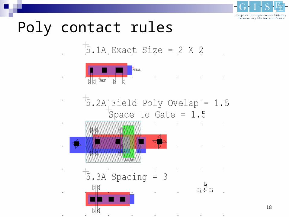
Poly contact rules

Adapted from Digital Integrated Circuits, 2nd Ed. 19
Metal Layers

Adapted from Digital Integrated Circuits, 2nd Ed. 20
The Metal layers
Metal layers are used to interconnect devices (transistors, resistors, inductors and capacitors)
Vias are used to interconnect the different metal layers Example: AMI 0.5 (three metals)

Adapted from Digital Integrated Circuits, 2nd Ed. 21
Metal Design rules
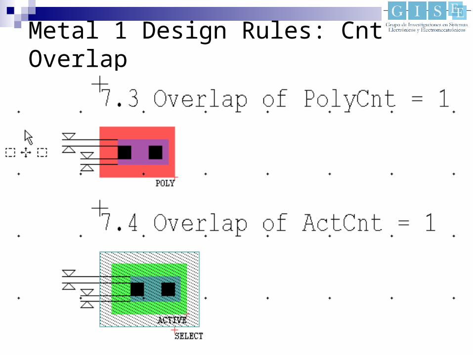
Metals 1, 2 and 3 rules Spacing rules Overlap rules
Vias 1 and 2 rules In general, higher metal layers require bigger dimensions and
spacing

Adapted from Digital Integrated Circuits, 2nd Ed. 22
Metal 1 Design Rules: Separation
Adapted from Digital Integrated Circuits, 2nd Ed. 23
Metal 1 Design Rules: Cnt Overlap

Adapted from Digital Integrated Circuits, 2nd Ed. 24
Metal 2 rules: Separation

Adapted from Digital Integrated Circuits, 2nd Ed. 25
Metal 2 Design Rules: via1 Overlap

Adapted from Digital Integrated Circuits, 2nd Ed. 26
Metal 3 rules: Separation

Adapted from Digital Integrated Circuits, 2nd Ed. 27
Metal 3 Design Rules: via2 Overlap

Adapted from Digital Integrated Circuits, 2nd Ed. 28
Via 1 rules

Adapted from Digital Integrated Circuits, 2nd Ed. 29
Via 2 rules

Adapted from Digital Integrated Circuits, 2nd Ed. 30
Interconnects

Adapted from Digital Integrated Circuits, 2nd Ed. 31
The Wire
transmitters receivers
schematics physical

Adapted from Digital Integrated Circuits, 2nd Ed. 32
Interconnect Impact on Chip

Adapted from Digital Integrated Circuits, 2nd Ed. 33
Wire Models
All-inclusive model Capacitance-only

Adapted from Digital Integrated Circuits, 2nd Ed. 34
Impact of Interconnect Parasitics
Interconnect parasitics reduce reliability affect performance and power consumption
Classes of parasitics Capacitive Resistive Inductive

Adapted from Digital Integrated Circuits, 2nd Ed. 35
10 100 1,000 10,000 100,000
Length (u)
No
of
ne
ts(L
og
Sc
ale
)
Pentium Pro (R)
Pentium(R) II
Pentium (MMX)
Pentium (R)
Pentium (R) II
Nature of Interconnect
Local Interconnect
Global Interconnect
SLocal = STechnology
SGlobal = SDie
So
urc
e:
Inte
l
Adapted from Digital Integrated Circuits, 2nd Ed. 36
INTERCONNECT: Capacitance

Adapted from Digital Integrated Circuits, 2nd Ed. 37
Capacitance of Wire Interconnect
VDD VDD
Vin Vout
M1
M2
M3
M4Cdb2
Cdb1
Cgd12
Cw
Cg4
Cg3
Vout2
Fanout
Interconnect
VoutVin
CLSimplified
Model
Adapted from Digital Integrated Circuits, 2nd Ed. 38
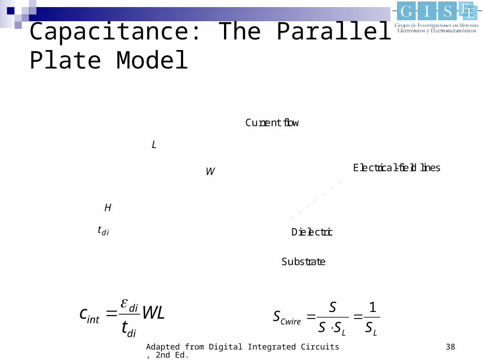
Capacitance: The Parallel Plate Model
Dielectric
Substrate
L
W
H
tdi
Electrical-field lines
Current flow
WLt
cdi
diint
LLCwire SSS
SS
1
Adapted from Digital Integrated Circuits, 2nd Ed. 39
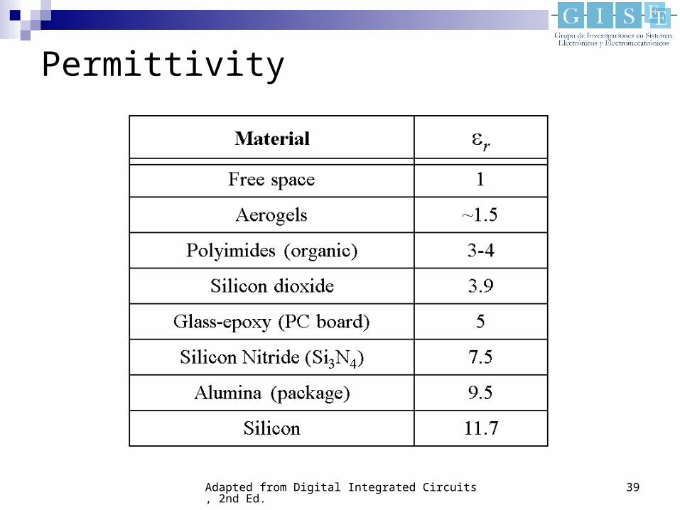
Permittivity

Adapted from Digital Integrated Circuits, 2nd Ed. 40
Fringing Capacitance
W - H/2H
+
(a)
(b)

Adapted from Digital Integrated Circuits, 2nd Ed. 41
Fringing versus Parallel Plate
(from [Bakoglu89])
Adapted from Digital Integrated Circuits, 2nd Ed. 42
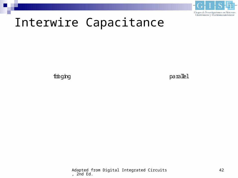
Interwire Capacitance
fringing parallel

Adapted from Digital Integrated Circuits, 2nd Ed. 43
Impact of Interwire Capacitance
(from [Bakoglu89])

Adapted from Digital Integrated Circuits, 2nd Ed. 44
Wiring Capacitances (0.25 mm CMOS)
Adapted from Digital Integrated Circuits, 2nd Ed. 45
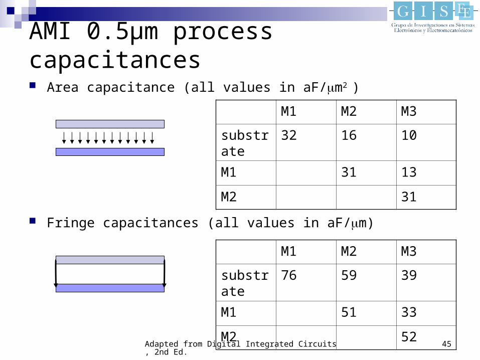
AMI 0.5µm process capacitances
Area capacitance (all values in aF/m2 )
Fringe capacitances (all values in aF/m)
M1 M2 M3
substrate 32 16 10
M1 31 13
M2 31
M1 M2 M3
substrate 76 59 39
M1 51 33
M2 52

Adapted from Digital Integrated Circuits, 2nd Ed. 46
INTERCONNECT: Resistance

Adapted from Digital Integrated Circuits, 2nd Ed. 47
Wire Resistance
W
L
H
R = H W
L
Sheet ResistanceRo
R1 R2

Adapted from Digital Integrated Circuits, 2nd Ed. 48
Interconnect Resistance
Adapted from Digital Integrated Circuits, 2nd Ed. 49
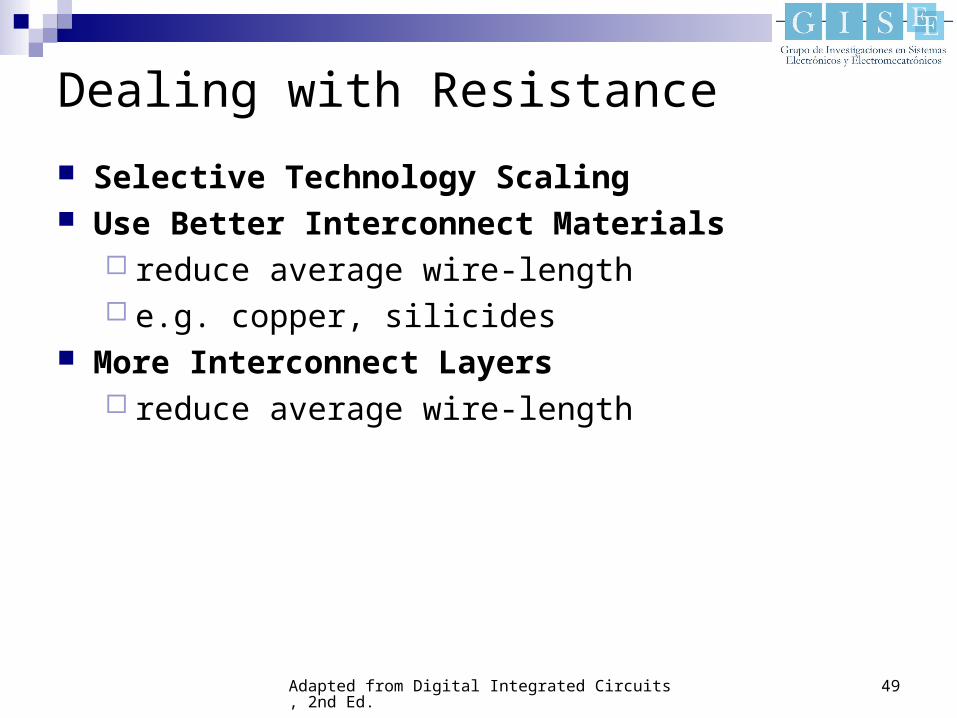
Dealing with Resistance
Selective Technology Scaling Use Better Interconnect Materials
reduce average wire-length e.g. copper, silicides
More Interconnect Layers reduce average wire-length
Adapted from Digital Integrated Circuits, 2nd Ed. 50
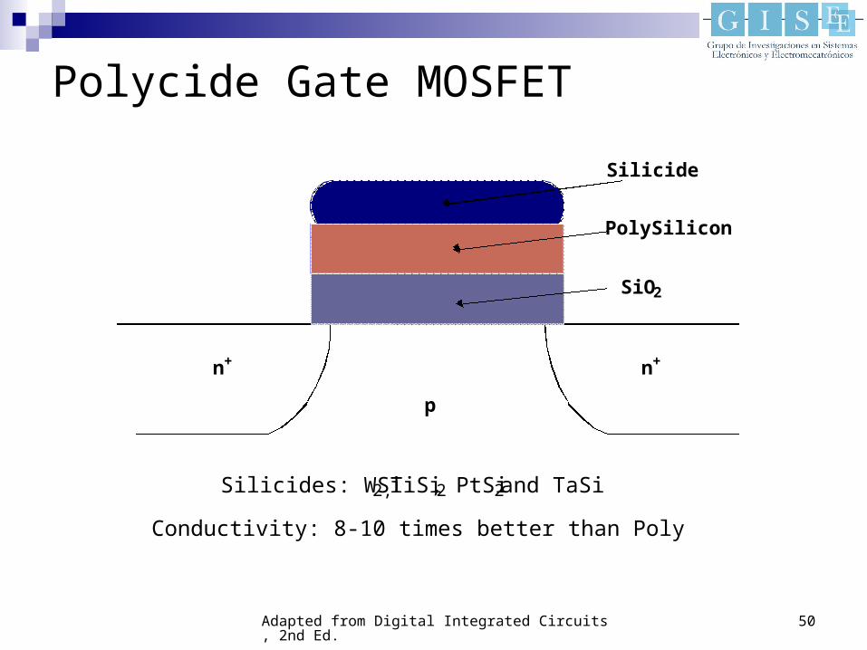
Polycide Gate MOSFET
n+n+
SiO2
PolySilicon
Silicide
p
Silicides: WSi 2, TiSi2, PtSi2 and TaSi
Conductivity: 8-10 times better than Poly

Adapted from Digital Integrated Circuits, 2nd Ed. 51
Sheet Resistance

Adapted from Digital Integrated Circuits, 2nd Ed. 52
Modern Interconnect
Adapted from Digital Integrated Circuits, 2nd Ed. 53
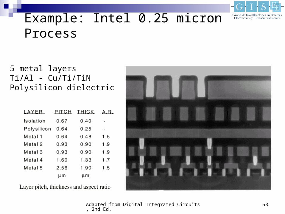
Example: Intel 0.25 micron Process
5 metal layersTi/Al - Cu/Ti/TiNPolysilicon dielectric

Adapted from Digital Integrated Circuits, 2nd Ed. 54
Resistance in AMI 0.5µm process
Resistance
A line of minimum width and 1mm long (1100 and 666 □ long, resp.)
M1 M2 M3
Rs 0.09Ω/□ 0.09 Ω/□ 0.05 Ω/□
M1 M2 M3
Rs 100 Ω 100 Ω 33 Ω

Adapted from Digital Integrated Circuits, 2nd Ed. 55
Vias parasitics
Vias exhibit a contact resistance given by the process
They also have a current limitation given by the electromigration phenomenom. Typically, 0.5mA/cnt
P+ N+ Poly M1 M2 M3
Contact R [Ω]
126 57.5 16 □ 0.82 0.79

Adapted from Digital Integrated Circuits, 2nd Ed. 56
Metal Current Capacity
Due to Electromigration, wire can be damaged For Aluminum, the maximum current density (rule of thumb)
is:
m
mA
1

Adapted from Digital Integrated Circuits, 2nd Ed. 57
INTERCONNECT: Inductance

Adapted from Digital Integrated Circuits, 2nd Ed. 58
Metal Parasitics: L
A metal line exhibits an inductance that can be estimated as:
Assumption: w > h L is proportional to w and inversely prop. to h
)/(44.1ln667.0393.1
25.1mmnH
hw
hw
L
Adapted from Digital Integrated Circuits, 2nd Ed. 59
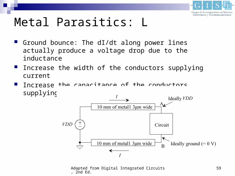
Metal Parasitics: L
Ground bounce: The dI/dt along power lines actually produce a voltage drop due to the inductance
Increase the width of the conductors supplying current Increase the capacitance of the conductors supplying current

Adapted from Digital Integrated Circuits, 2nd Ed. 60
InterconnectInterconnectModelingModeling
Adapted from Digital Integrated Circuits, 2nd Ed. 61
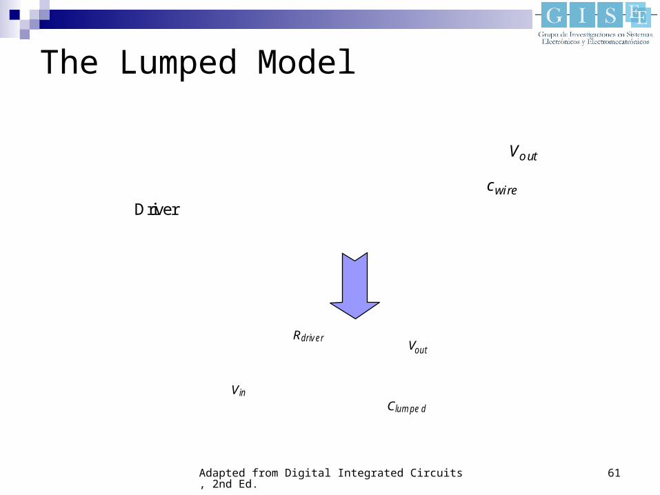
The Lumped Model
Vout
Driver
cwire
VinClumpe d
RdriverVout

Adapted from Digital Integrated Circuits, 2nd Ed. 62
The Lumped RC-Model: Elmore Delay

Adapted from Digital Integrated Circuits, 2nd Ed. 63
The Ellmore Delay: RC Chain
Adapted from Digital Integrated Circuits, 2nd Ed. 64
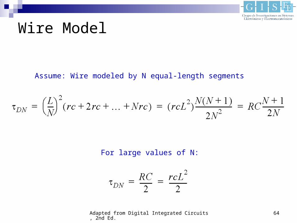
Wire Model
Assume: Wire modeled by N equal-length segments
For large values of N:

Adapted from Digital Integrated Circuits, 2nd Ed. 65
The Distributed RC-line

Adapted from Digital Integrated Circuits, 2nd Ed. 66
Step-response of RC wire as a function of time and space
0 0.5 1 1.5 2 2.5 3 3.5 4 4.5 50
0.5
1
1.5
2
2.5
time (nsec)
volta
ge (V
)
x= L/10
x = L/4
x = L/2
x= L
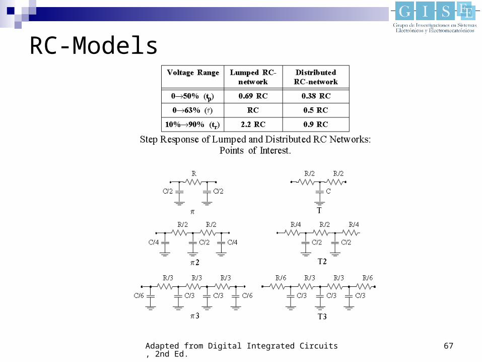
Adapted from Digital Integrated Circuits, 2nd Ed. 67
RC-Models

Adapted from Digital Integrated Circuits, 2nd Ed. 68
Driving an RC-line
Vi n
Rs Vo ut(rw,cw,L)

Adapted from Digital Integrated Circuits, 2nd Ed. 69
Design Rules of Thumb
rc delays should only be considered when tpRC >> tpgate of the driving gate
Lcrit >> tpgate/0.38rc
rc delays should only be considered when the rise (fall) time at the line input is smaller than RC, the rise (fall) time of the line
trise < RC when not met, the change in the signal is slower than the
propagation delay of the wire
© MJIrwin, PSU, 2000
Adapted from Digital Integrated Circuits, 2nd Ed. 70
Appendix

Adapted from Digital Integrated Circuits, 2nd Ed. 71
AMI 0.5 typical parameters (T36s)

Adapted from Digital Integrated Circuits, 2nd Ed. 72
Appendix
Poly resistor layout

Adapted from Digital Integrated Circuits, 2nd Ed. 73
Poly: Resistor Design
MOSIS webpage data for AMI 0.5 R(N_Well) = 22Ω/□ Exercise: Layout and extract a resistor (minimum width) of
1K. Try to make a square design Number of squares to achieve the desired resistance =
1000/22 □ = 45.5 Setting W = 2 then L = 91 Run DRC, extract and verify

Adapted from Digital Integrated Circuits, 2nd Ed. 74
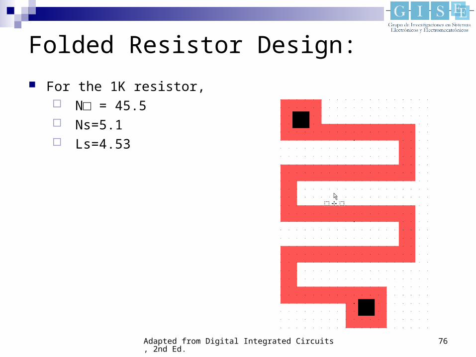
Folded Resistor Design:
Folding the resistor leads to compact designs Squares and corners contribute partially to the material
resistance

Adapted from Digital Integrated Circuits, 2nd Ed. 75
Folded Resistor Design:
Calculation for a square layout
Assume Ns segments of width Ws, length Ls and spacing Wg
The number of squares is:
For a square design:
Ws
WgNs
Ws
LsNs
Ws
WsLsN )56.0(2)1()2(
22)8.0(2
WsWgWsNsWsLs ))(1(2
Adapted from Digital Integrated Circuits, 2nd Ed. 76
Folded Resistor Design:
For the 1K resistor, N□ = 45.5 Ns=5.1 Ls=4.53