Embed Size (px)
Citation preview

Design of Analog Integrated CircuitsFall 2012, Dr. Guoxing Wang 1
Design of Analog Integrated Circuits
Frequency Response
2
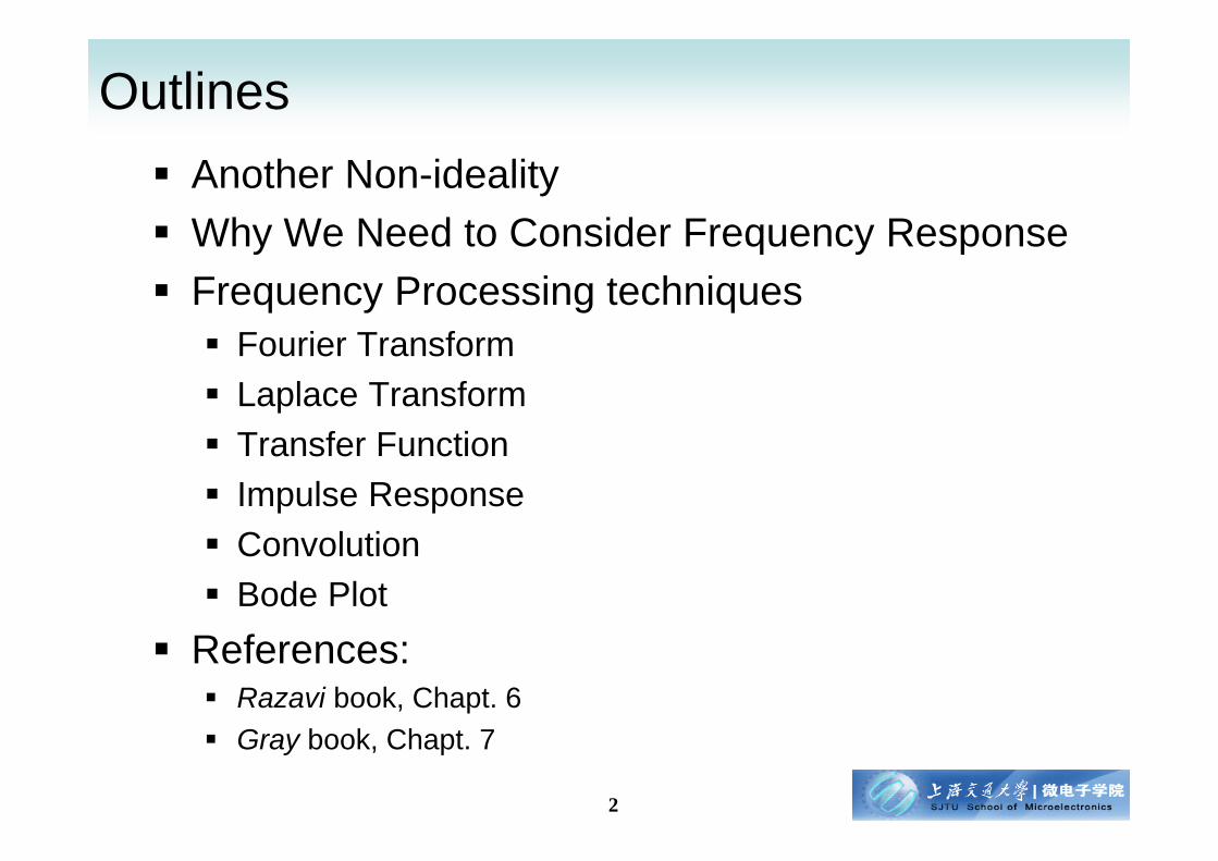
Outlines Another Non-ideality Why We Need to Consider Frequency Response Frequency Processing techniques Fourier Transform Laplace Transform Transfer Function Impulse Response Convolution Bode Plot
References: Razavi book, Chapt. 6 Gray book, Chapt. 7

3
One More Non-Idealities
AVo A function of frequency
Bandwidth!
In time domain, output can not change that fast!
4
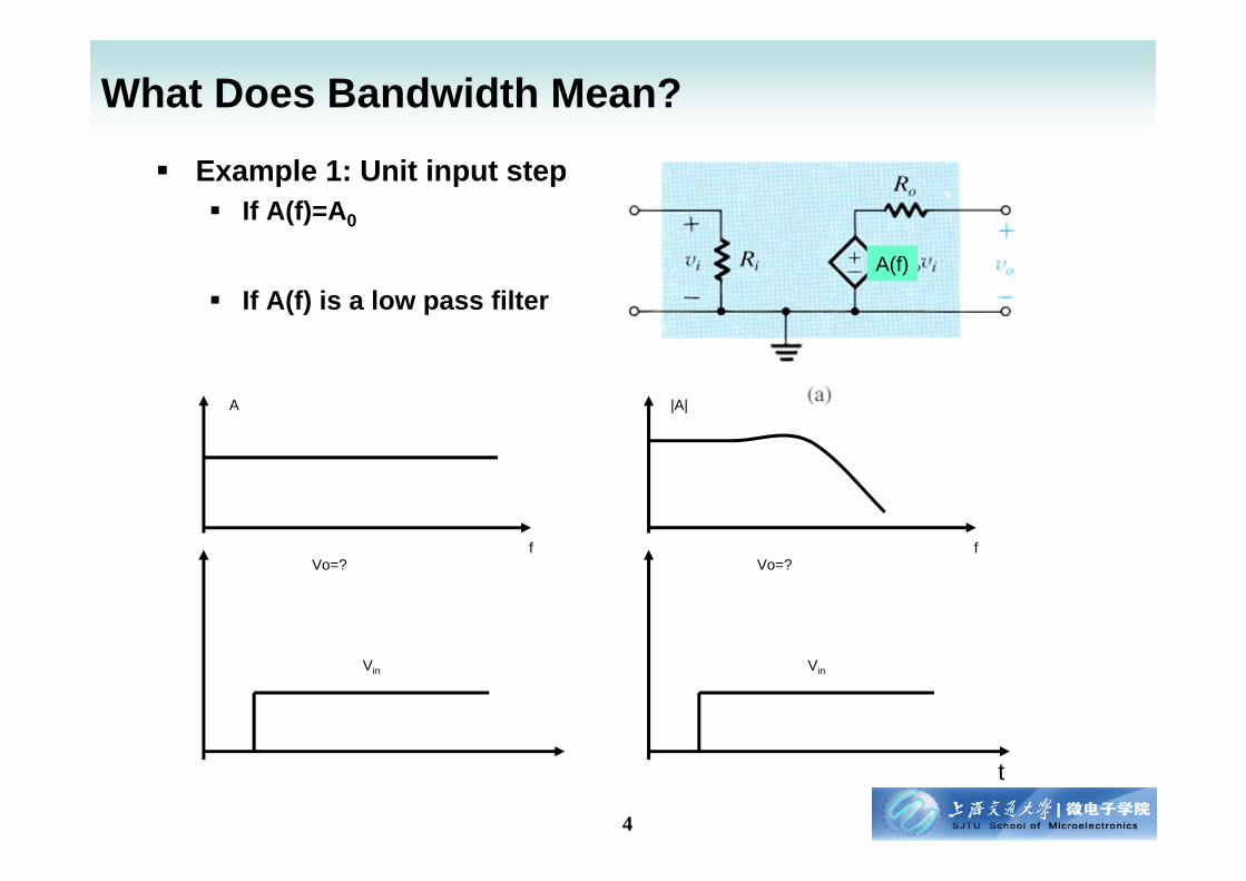
What Does Bandwidth Mean?
Example 1: Unit input step If A(f)=A0
If A(f) is a low pass filterA(f)
f
|A|
t
Vo=?
Vin
f
A
Vo=?
Vin

5
Solutions
Convolution! Frequency Domain, and then back to time domain

6
Signal (Time-domain) X’form (Freq-domain)
( )t
( )u t
( )ate u t
1
( )( 1)!
nt u tn
0[cos ] ( )t u t
0[sin ] ( )t u t
1s1
s a1
( )ns a
2 20
ss
02 2
0s
1
Laplace Transform Pairs

7
Revisit: Capacitances in MOSFET
Fundamentals about capacitance
Charge accumulation device
Energy storage device
Why it matters?
Time, Speed
Bandwidth

8
Capacitance in MOSFET
Intrinsic Capacitance Summary
CGB CGS CGD
Cutoff (WLCox)Cd/(WLCox+Cd) Cov Cov
Linear 0 1/2WLCox+Cov 1/2WLCox+Cov
Saturation 0 2/3WLCox+Cov Cov
Cov=WLovCox , where Lov is the overlap length between the source and drain and Cd is the depletion region capacitance

9
Circuit Elements and Frequency Properties
Vi(t)+
-Vo(t)
+
-

10
Example of Frequency Response
Transfer Function
log1
)1(1
1
1
11
11
11
11
1
)()(
2
2
RC
RC
RCp
RC
jRCjsRCsC
RsC
sVsV
i
o
Vi(t)+
-Vo(t)
+
-

11
Input unit step function u(t),
)()()(
111
)1(1)(1)(
11)(
1)(
tuetuty
RCsssRCs
sHs
sY
sRCsH
stu
RCt
L
u(t)
t
1
y(t)
t
1
Example of Frequency Response (2)

12
Cascading
1
• Second order system
• Difficult to find out poles
• In IC design, circuit is (or preferred to be) more like isolated stages

13
Bode Plot of H(s)• When all the poles and zeros are far (4x) away from each other, it is easy to get
the Bode Plot• For magnitude
• A LHP real pole contributes -20dB/Dec• A LHP real zero contributes 20dB/Dec
• For phase• A LHP real pole contributes -90 ºC• A LHP real zero contributes +90 ºC• A RHP real zero contributes -90 ºC
• Usually a bad thing!• Of course, at the frequency of the zeros/poles are special,
• 3dB and 45ºC• What does this mean for IC design?
• A useful tool for analyze and design circuits, stability, bandwidth

14
1021
1)(
s
sH
Bode Plot:Example 1

15
1021
1)(
s
sH
Bode Plot:Example 1 – Log Domain
16
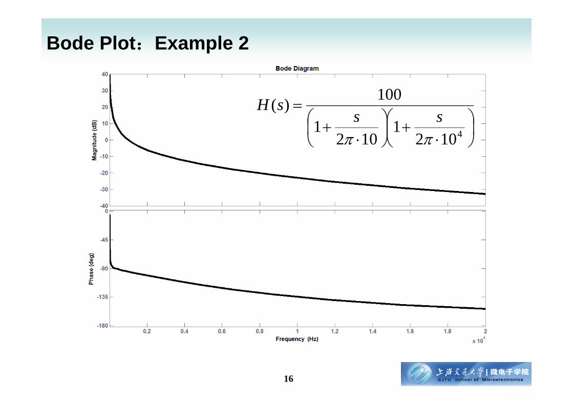
41021
1021
100)(
ss
sH
Bode Plot:Example 2

17
41021
1021
100)(
ss
sH

18
6
3
1021
121
1021100
)(
ss
s
sH
Bode Plot:Example 3 (Effect of Zero)

19
Transfer Function and Circuits Frequency Response Use a plot to intuitively help understand characteristics of a
system (transfer function) Implied assumption
Linear Time-Invariant system only If x y, we know a*x a*y
What if not a linear system? We linearize (with approximation) it
.AC in HSPICE Check back using full system behavior
.tran in HSPICE
Common Source (and other) Amplifiers a linear system? We linearize it at the operation point, find out the small signal gain
(which was considered at zero frequency only in previous lectures) but actually a function of frequency Equation approach to get some intuitive understanding For analog circuits, we need to be able to ‘guess’ where is the
pole/zero, and know how to ‘tune’ them

20
One commonly used technique to reduce the circuit complexity for the purpose of analysis
The goal is to remove the link between the input and output so the circuits look ‘clean’.
Two port analysis Input port equivalent Output port impedance
is ignored (approximated) here
Miller Effect
Miller Effect: The capacitance looks bigger due to the amplification (A)

21
Analysis of CS Amplifier Freq. Resp.
Before we do math, let’s guess:
1. How many zeros, poles?
2. Where do the poles and zeros frequency may located?
From the small signal model, we can do the
math

22
And the result is …
Vo/Vin =-(gmRL)[1-s(C/gm)]
---------------------------------------------------------------------------1+s{[CG+C(1+gmRL)]Rin+(CL+C)RL}+s2[(CL+C)Cgs+CLC]RinRL
Looks difficult …And technologies are driven by lazy people …We want to get a first sense about the circuit by just looking at it
(without deriving difficult equations)

23
Insights
DC gain, gmRL
There is a zero, and z=+gm/C Zero moves the phase and magnitude of the frequency response,
we can choose C, gm for frequency response we want And this ‘two signal paths’ intuition is an important technique for
analog circuits If C is just Cgd
It is usually very small (order of 10~100fF), zero is big (order of 10GHz~100GHz for mS of gm, far away!)
If C is on the order of pF, the zero might come into play!
There are two poles Now what?

24
Insights (cont’d)-(gmRL)[1-s(C/gm)]
---------------------------------------------------------------------------1+s{[CG+C(1+gmRL)]Rin+(CL+C)RL}+s2[(CL+C)Cgs+CLC]RinRL
One technique There are two poles, D(s) = (1+s/p1) (1+s/p2)
D(s) = 1+s(1/p1+1/p2)+s2/(p1p2)D(s) ~= 1+s(1/p1)+s2/(p1p2) (if p1<<p2)
p1 is called dominant pole
So p1 is approximately1/{[CG+C(1+gmRL)]Rin+(CL+C)RL}
If Rin is big (the case if the previous stage is high output impedance amplifier)

25
Insights (cont’d) – Rin
So p1 is approximatelyp1 ~= 1/{[CG+C(1+gmRL)]Rin+(CL+C)RL}
If Rin is big (the case if the previous stage is high output impedance amplifier)
p1 ~= 1/{[CG+C(1+gmRL)]Rin}Miller effect!
The dominant pole is mainly due to the input node
If Rin is small (the case if the previous stage is SF) The dominant pole is mainly due to the output node
p1 ~= 1/{(CL+C)RL}
If Rin = 0, it reduces to a first-order system, only one pole
26
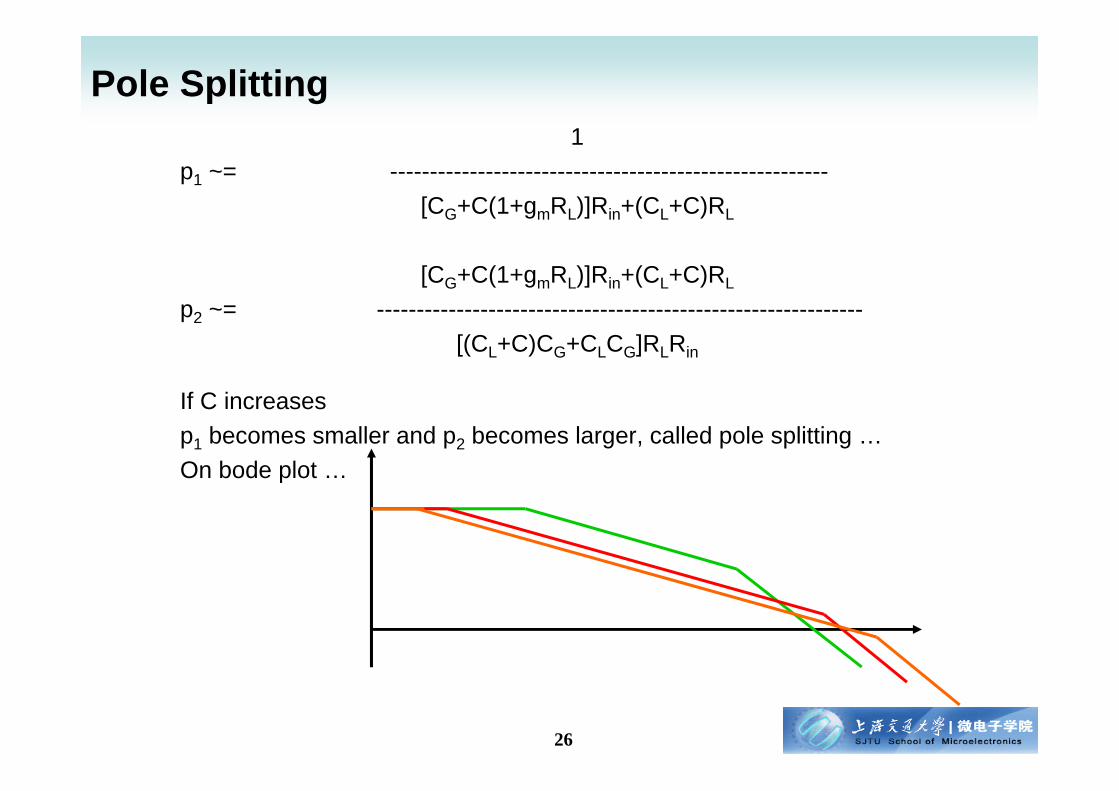
Pole Splitting1
p1 ~= -------------------------------------------------------[CG+C(1+gmRL)]Rin+(CL+C)RL
[CG+C(1+gmRL)]Rin+(CL+C)RL
p2 ~= -------------------------------------------------------------[(CL+C)CG+CLCG]RLRin
If C increasesp1 becomes smaller and p2 becomes larger, called pole splitting …On bode plot …
27
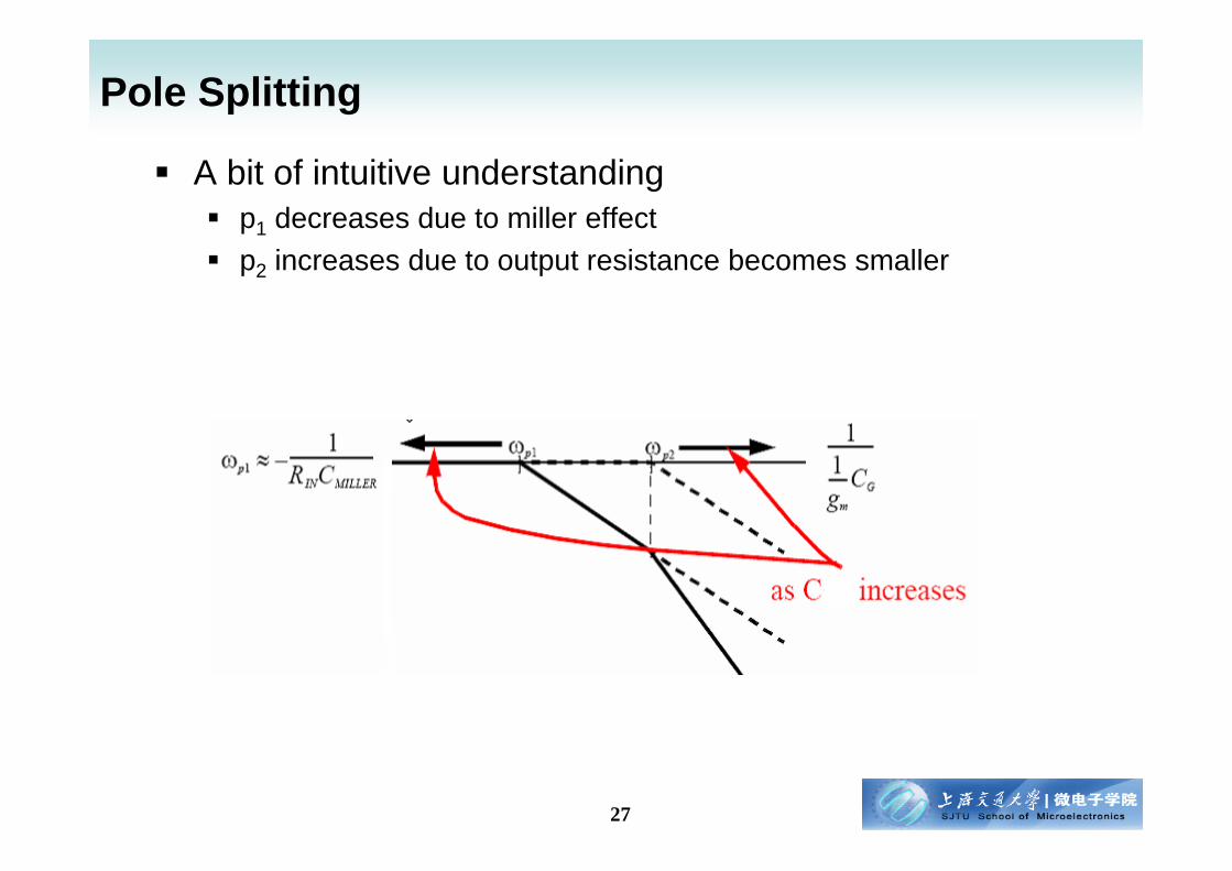
Pole Splitting
A bit of intuitive understanding p1 decreases due to miller effect p2 increases due to output resistance becomes smaller
28
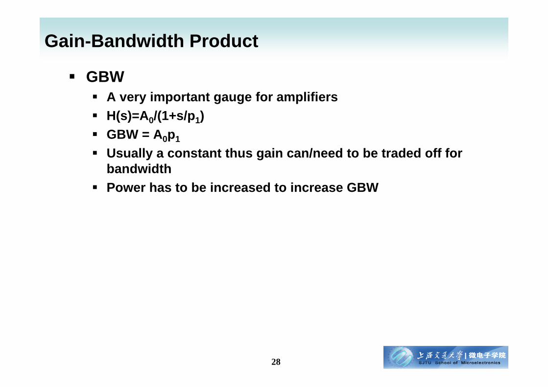
Gain-Bandwidth Product
GBW A very important gauge for amplifiers H(s)=A0/(1+s/p1) GBW = A0p1
Usually a constant thus gain can/need to be traded off for bandwidth
Power has to be increased to increase GBW

29
Summary of CS
H(s) = A0(1-s/z)
---------------------------(1+s/p1)(1+s/p2)
And p1,p2 are between two extremes.

30
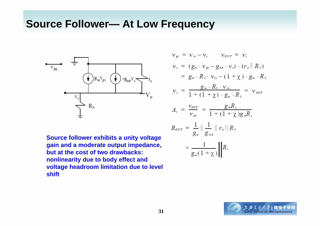
Good for buffering and impedance transformation Level Shifter—the output DC is one VGS lower than the input DC
Source Follower
31
Source follower exhibits a unity voltage gain and a moderate output impedance, but at the cost of two drawbacks: nonlinearity due to body effect and voltage headroom limitation due to level shift
Source Follower— At Low Frequency

32
SF Freq Model Again, poles and
zeros?

Design of Analog Integrated CircuitsSpring 2011, Dr. Guoxing Wang 33

Design of Analog Integrated CircuitsSpring 2011, Dr. Guoxing Wang 34

Design of Analog Integrated CircuitsSpring 2011, Dr. Guoxing Wang 35
Input node dominant
Output node dominant • If it is used to drive large capacitance, usually dominated by output node
• If the source resistance of previous is really large, like cascode amplifier, usually dominated by input node

36
Merits:
• High Gain
• Non-Inverting
• Low input resistance when the output is terminated with reasonable impedance (<<ro)
• High output resistance
Common-Gate (CG) Amplifier

Design of Analog Integrated CircuitsSpring 2011, Dr. Guoxing Wang 37
Zeros, poles?

38
No capacitive link between input node
and output node,
NICE!

Design of Analog Integrated CircuitsSpring 2011, Dr. Guoxing Wang 39

Design of Analog Integrated CircuitsSpring 2011, Dr. Guoxing Wang 40

Design of Analog Integrated CircuitsSpring 2011, Dr. Guoxing Wang 41

42
Summary of Frequency Response Another non-ideality we need to consider Affect the speed of the circuits Use poles and zeros to analyze Exact equations are usually tedious and insights are needed by looking at
circuits Always try to simplify into single nodes Knowing which nodes are nodes with large capacitance and large resistance
CS Miller effect Has two poles and one zero Pole splitting
SF Two poles and one zero Can be used to drive large capacitance
CG No zero (because no capactive signal path) Can be thought of as an isolator
Keep in mind: the transfer function is just a simplification of the real circuits, i.e. a linearized approximation