Embed Size (px)
Citation preview
A METHOD FOR MODELLING RADIO
FREQUENCY DEPOSITION OR ETCH PLASMA
CHAMBERS USING AN EQUIVALENT
ELECTRONIC COMPONENT CIRCUIT
by
Brian Cregan, B.A.I., B.A.
A thesis submitted in partial fulfilment
of the requirements for the degree of
MEng.
School o f Electronic Engineering
Dublin City University
September 2004
Academic Supervisor: Professor David C. Cameron

DECLARATION
I hereby certify that this material, which I now submit for assessment on the
programme o f study leading to the award o f Master o f Engineering is entirely my
own work and has not been taken from the work o f others save and to the extent
that such work has been cited and acknowledged within the text o f the work.
Signed : " Date: !~7// / O S
Brian Cregan

ACKNOWLEDGEMENTS
I would like to thank Professor David Cameron, my Academic Supervisor, for his
guidance through this entire project. It was a pleasure and privilege to work with
such a dedicated and enthusiastic supervisor. I have benefited greatly from the
positive learning environment that has been provided by David and wish him
every success in the future.
I would like to thank Stephen Daniels, my manager while I worked at Scientific
Systems Ltd., for his invaluable advice on balancing work life and educational
life. His belief in further education and the opportunities it brings is both
refreshing and encouraging.
Much of this work was carried out while I was working with Scientific Systems
Ltd. I am grateful for the financial support and expertise that was provided to me
from the staff at Scientific Systems Ltd. I would especially like to thank Mike
Hopkins, Francisco Martinez, Jean Pierre Pererienha, Jean Marc Ouvard, Kieron
Dobbyn, Donal O’Sullivan, Conor Hilliard, Brian Heil, Predrag Stankovic and
Conor Mullaney.
I would like to thank my friends who have endured the fascinating world of radio
frequency theory and plasma physics in the recent past. Their support through
tough times is greatly appreciated.
Finally, I would like to thank my parents, Donal and Maire, and my sister Claire.
They have provided the opportunities for me that have lead to me producing this
work. They have been the one constant over the years and have given me the
confidence and self belief to keep on educating and improving myself.
DECLARATION.......................................................................................................... ii
ACKNOWLEDGEMENTS........................................................................................ iii
CONTENTS................................................................................................................. iv
Abstract.......................................................................................................................... 1
Chapter 1 Introduction..................................................................................................2
1.1 Introduction...................................................................................................2
1.2 Review of Plasma Chamber Modelling......................................................5
1.3 Research Objectives and Summary............................................................5
1.4 Organisation of the Thesis........................................................................... 6
Chapter 2 Theory...........................................................................................................7
2.1 Introduction................................................................................................... 7
2.2 Radio Frequency Theory............................................................................. 8
2.2.1 The Electromagnetic Spectrum............................................................ 8
2.2.2 Radio Frequency versus DC or Low AC Signals............................. 11
2.2.3 Component Basics...............................................................................12
2.2.4 Radio Frequency Impedance Matching............ ............................... 19
2.2.5 Transmission Lines............................................................................ 21
2.2.5.2 Propagation Modes............................................................................. 23
2.2.5.3 Lumped-Element Model.....................................................................24
2.2.5.4 Transmission Line Equations............................................................28
2.2.5.5 The Lossless Transmission Line........................................................30
2.2.5.6 Voltage Reflection Coefficient..........................................................33
2.2.5.7 Standing Waves................................................................................... 35
2.2.5.8 Input Impedance of the lossless Line................................................ 37
2.2.6 The Smith Chart..................................................................................39
2.2.7 Insertion Loss......................................................................................42
2.3 Plasma Theory...........................................................................................44
2.3.1 An overview of Plasma......................................................................44
2.3.2 Plasma Sheaths....................................................................................47
2.3.3 RF diodes............................................................................................ 49
2.3.4 Theoretical Model of a Capacitively Coupled Plasma Discharge 54
2.3.4.1 Plasma Admittance............................................................................. 56
CONTENTS
2.3.4.2 Sheath Admittance..............................................................................56
2.4 Mesh Current Network Analysis........................................................... 60
2.4.1 Mesh Currents.....................................................................................60
2.4.2 Choice of Mesh Currents................................................................... 62
2.4.3 Number of Mesh Currents Required................................................. 63
2.4.4 Mesh Equations by Inspection...........................................................63
2.4.5.1 Matrices................................................................................................64
2.4.5.2 Addition of Matrices..........................................................................64
2.4.5.3 Multiplication of Matrices................................................................. 64
2.4.5.4 Inversion..............................................................................................65
2.4.5.5 Determinant of a Square Matrix........................................................65
2.4.5.6 Solution of Linear Equations by Determinant and Cramer’s Rule
66
2.4.6.1 Matrix Methods and Circuit Analysis............................................... 67
2.4.6.2 Driving Point Impedance................................................................... 68
2.4.6.3 Transfer Impedance............................................................................ 69
2.4.7 The Simplex Method..........................................................................69
Chapter 3 System Set-up............................................................................................. 71
3.1 Introduction................................................................................................. 71
3.2 System Components................................................................................... 72
3.2.1 The Power Supply.............................................................................. 72
3.2.2 The Network Analyser.......................................................................73
3.2.3 The Plasma Chamber.......................................................................... 73
3.2.4 The Match Unit...................................................................................75
3.2.5 The SmartPIM System.......................................................................79
3.2.6 The SmartProbe...................................................................................80
3.3.1 Mechanical Systems........................................................................... 80
Chapter 4 Method........................................................................................................81
4.1 Introduction................................................................................................. 81
4.2 Experimental Set-up and Results...............................................................81
4.2.1 SmartProbe and SmartPIM measurements of an Argon Plasma ..81
4.2.2 Electronic Component Model of the Plasma Chamber System.... 82
4.2.2.1 Frequency Response of the Chamber............................................... 82
4.2.2.2 Electronic Component Model........................................................... 87
4.2.2.3 Scilab Program................................................................................... 88
Chapter 5 Results and Conclusions....................................................................90
5.1 Introduction..................................................................................................90
5.2 SmartProbe Analysis of the Plasma Chamber........................................ 90
5.3 Electronic Component Model of the Plasma Chamber............................91
5.4 Further Experimentation and Work.......................................................... 97
5.5 Applications................................................................................................ 97
References...................................................................................................................R1
Appendix A Scilab Program Files.............................................................................A1
Column 1 .............................................................................................................A1
Error2.................................................................................................................. A1
makesum.............................................................................................................A2
Parallel................................................................................................................A2
plotshpape2.......................................................................................................A 11
pshapcl.............................................................................................................A 12
Siniplex4.......................................................................................................... A18
Update...............................................................................................................A24
AbstractExtensive work continues to be carried out on correlating the electric
characteristics of parallel-plate discharges with an equivalent model. Theoretical
models have been developed for capacitive radio frequency driven plasmas.
Voltage, current and phase measurements of radio frequency discharges have
been used to gain empirical data of a wide range of discharge parameters. It has
been found that parasitic impedances within a plasma chamber have a substantial
effect on impedance measurements of plasmas. This means that simple a priori
models are inadequate for understanding plasmas. Complicated experimental
setups have been used to better understand the propagation of radio frequency
electromagnetic radiation through plasmas/plasma chambers. These however can
not be transferred to a manufacturing environment due to non uniformity issues
across a given wafer. The effect of the plasma chamber setup on plasma
characteristics has been demonstrated.
Although plasma processes are widely used in industry, the general
understanding of these processes is poor and process control is difficult. The
ability to etch fine lines and the control of anisotropy, etching rate, uniformity,
selectivity and end point detection are obtained by experimental trial and error.
This thesis describes a method of characterising the condition of a radio or
microwave frequency excited plasma etching or deposition system as would be
used in the semiconductor industry. This process can be used for:
(i) monitoring the state of a system as it ages to detect when cleaning or
repair is required
(ii) checking that the characteristics of the system are as expected after
manufacture, rebuild or modification.
The location of any defects may be detected by simulating the frequency response
of the altered system to see which electrical component values have changed.
These can then be related to the physical components of the system. This
characterisation can be integrated into the normal process flow; when the plasma
is not powered up e.g., during pump down or loading for example, the network
analyser can be switched in and the measurements made. In this way, the system
can be characterised on a “real-time” basis.
l

Chapter 1 Introduction
1.1 Introduction
The ever shrinking dimensions of microelectronic devices have necessitated the
use of plasma processing in integrated circuit (IC) factories worldwide. Revenues
in the plasma processing industry now exceed $3 billion per annum, well in
excess of predictions made only a few years ago [1], Besides the use of plasmas
in etching and depositing thin films, other processes include the removal of
photoresist remnants after development (descumming), stripping developed
photoresist after pattern transfer (ashing), and passivating defects in
polycrystalline material [2]. Plasma based surfaces are also critical for the
aerospace, automotive, steel, biomedical and toxic waste management industries.
Materials and surface structures can be fabricated that are not attainable by any
other commercial method, and the surface properties of materials can be modified
in unique ways.
The semiconductor industry has advanced from revolutionary
development to evolutionary advances with a focus on manufacturing. While
product and process advances are still very much industry issues, greater
emphasis is being placed on the business factors, and while high yields are a
must, new processes and equipment are being measured by overall productivity.
Strategies to increase the bottom line include maximising cost of ownership,
automation, cost control, computer-automated manufacturing, computer-
integrated manufacturing and statistical process control.
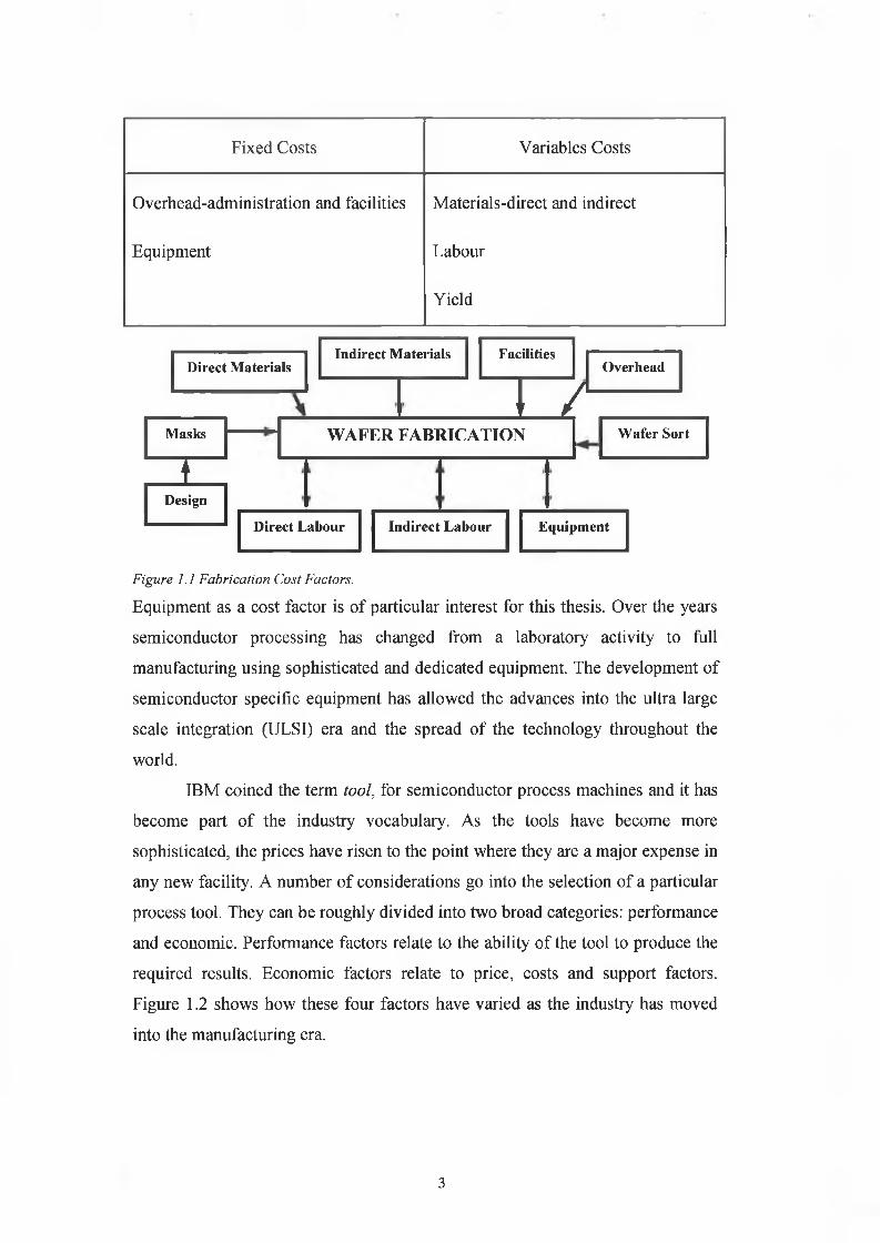
A number of factors contribute to the cost of producing a functioning dice
(figurel.l). They are generally divided into fixed and variable categories. Fixed
costs are those that exist whether or not any die are being made or shipped.
Variable costs are those that go up or down with the volume of product being
produced.
2
Fixed Costs Variables Costs
Overhead-administration and facilities
Equipment
Materials-direct and indirect
Labour
Yield
Direct MaterialsIndirect Materials
Masks
I
FacilitiesOverhead
u rWAFER FABRICATION Wafer Sort
Design
Direct Labour Indirect Labour Equipment
Figure 1.1 Fabrication Cost Factors.
Equipment as a cost factor is of particular interest for this thesis. Over the years
semiconductor processing has changed from a laboratory activity to full
manufacturing using sophisticated and dedicated equipment. The development of
semiconductor specific equipment has allowed the advances into the ultra large
scale integration (ULSI) era and the spread of the technology throughout the
world.
IBM coined the term tool, for semiconductor process machines and it has
become part of the industry vocabulary. As the tools have become more
sophisticated, the prices have risen to the point where they are a major expense in
any new facility. A number of considerations go into the selection of a particular
process tool. They can be roughly divided into two broad categories: performance
and economic. Performance factors relate to the ability of the tool to produce the
required results. Economic factors relate to price, costs and support factors.
Figure 1.2 shows how these four factors have varied as the industry has moved
into the manufacturing era.
3

100%
80%
60%
40%
20%
0%
Figure 1.2 Changes in equipment, purchase factors (Source: Semiconductor International, May
1993, p. 58).
While performance has fallen as a selection criterion, any tool must have
the basic capability to meet the process requirements. If the machine cannot
routinely produce the right product, it is of no use. Other performance factors are
repeatability, flexibility, upgradeability, ease of operation, set-up and
reliability/downtime factors.
• Repeatability is the ability to produce the same result every time and over
long periods of time.
• Flexibility relates to the ease with which a machine can be switched to run
a variety of products and processes.
• Upgradeability is the ability of the machine to handle future process
requirements, such as increasing wafer diameters.
• Ease of operation and set-up factors address the issue of minimising
operator mistakes by good design and user friendly controls.
• Set-up issues relate to the amount of time required to bring the tool on
line (tests, calibrations etc.) and the related loss of production time.
Most companies run their equipment two or three shifts per day,
sometimes six to seven days a week. Scheduled maintenance and unscheduled
breakdowns stall product flow and run up the expenses. The factors are:
scheduled maintenance frequency and time, mean time to failure and mean time
to repair. Given the expense of most machines, having back-ups is a costly
luxury. It falls on the vendor to provide a machine that runs for long periods of
I960 1970 1980 1990
□ Performance ■ Price □ Support □ Cost o f Ownership
4
time, can be repaired quickly when failure occurs and does not need frequent and
lengthy routine maintenance. Cost also includes the price of materials needed for
the machine process. Machines that waste materials also waste money.
Vendor support has emerged as a critical factor. The advancement of
process technology and equipment sophistication has forced close cooperation
and alliances between the chip manufacturers and their suppliers. The cost of
machine development requires input from the using-process engineers and the
detailed nature of the machines requires on-time back-up from vendors.
1.2 Review o f Plasma Chamber Modelling
Extensive work continues to be carried out on correlating the electric
characteristics of parallel-plate discharges with an equivalent model. Theoretical
models have been developed for capacitive radio frequency driven plasmas [3],
Voltage, current and phase measurements of radio frequency discharges have
been used to gain empirical data for a wide range of discharge parameters [4], It
has been found that parasitic impedances within a plasma chambcr have a
substantial effect on impedance measurements of plasmas [5]. This means that
simple a priori models are inadequate for understanding plasmas. Complicated
experimental setups have been used to better understand the propagation of radio
frequency electromagnetic radiation through plasmas/plasma chambers [6]. These
however can not be transferred to a manufacturing environment due to non
uniformity issues across a given wafer. The effect of the plasma chamber setup
on plasma characteristics has been demonstrated [7].
1.3 Research Objectives and Summary
Although plasma processes are widely used in industry, the general
understanding of these processes is poor and process control is difficult. The
ability to etch fine lines, the control of anisotropy, etching rate, uniformity,
selectivity and end point detection are obtained by experimental trial and error.
This thesis describes a method of characterising the condition of a radio or
microwave frequency excited plasma etching or deposition system as would be
used in the semiconductor industry. The method involves measuring the electrical
impedance of the chamber over a wide frequency range (e.g. l-200MHz for a
5
system normally operating at 13.56MHz) by using an impedance analyser. The
frequency response may then be simulated by an electrical network of
components based on the physical arrangement of the system components. Any
changes in the system due to electrical connections can be detected by observing
changes in impedance without access to the interior of the system. This process
can be used for:
(iii) monitoring the state of a system as it ages to detect when cleaning or
repair is required
(iv) checking that the characteristics of the system are as expected after
manufacture, rebuild or modification.
The location of any defects may be detected by simulating the frequency response
of the altered system to see which electrical component values have changed.
These can then be related to the physical components of the system. This
characterisation can be integrated into the normal process flow; when the plasma
is not powered up e.g., during pump down or loading for example, the network
analyser can be switched in and the measurements made. In this way, the system
can be characterised on a “real-time” basis.
1.4 Organisation o f the Thesis
This thesis is organised into five chapters, references and one appendix.
• A review of plasma chamber modelling, the research objectives and
summary of this thesis have been described in Chapter 1.
• The required theoretical background for this thesis is given in Chapter 2.
Three areas are covered viz. radio frequency theory, plasma theory and
mesh current network analysis.
• The equipment used and the experimental set-up is described in Chapter
3.
• The experimental method and results are recorded in Chapter 4.
• The conclusions of this work and suggestions for future research are given
in Chapter 5.
• References.
• Appendix A contains the Scilab program files.
6
Chapter 2 Theory
2.1 Introduction
There are various fields of expertise that are used to design and build industrial
and research plasma chambers. There are three main areas referred to in this
thesis. The first is Radio Frequency Theory. Many industrial plasmas are driven
by radio frequency power sources. A strong knowledge of how radio frequency
electromagnetic radiation propagates through a plasma chamber system is
therefore essential. References [8], [9] and [10] are used to present the
fundamental concepts of radio frequency theory and how these concepts relate to
plasmas and plasma chamber systems.
The second field of expertise is Plasma Theory. The plasma is the central
component of the plasma chamber. Everything within a plasma chamber system
is designed around producing plasma that will complement a given process. The
basic properties of plasmas, their parameters and how they exist in different
systems must be understood. References [11] and [12] are used to' present the
fundamental concepts of capacitively coupled discharges.
In this thesis the plasma chamber is modelled using algorithms that are
based on matrices. A basic theory of matrices has been included in this chapter,
with specific reference to Cramer’s rule. A description of the Simplex Method for
curve fitting is also given. Large amounts of data are needed to generate the
models for the chamber. Storing this data in matrix form allows the use of
matrices functions, providing strong processing power. References [13] and [14]
are used to present the matrices theory required for the derivation of the
algorithms in this thesis.
7
2.2 Radio Frequency Theory
2.2.1 The Electromagnetic Spectrum
Radio Frequency signals belong to a family of waves called the Electromagnetic
Spectrum. All electromagnetic waves share the following fundamental properties:
• An electromagnetic wave consists of electric and magnetic field
intensities that oscillate at the same frequency/
• The phase velocity of an electromagnetic wave propagating is a universal
constant given by the velocity of light c, defined as
c _ __ \_
Vwhere fio is the magnetic permeability of free space and e0 is the
permeability of free space.
• In vacuum, the wavelength A of an electromagnetic wave is related to its
oscillation frequency/by
Whereas all electromagnetic waves share these properties, each is distinguished
by its own wavelength A, or equivalently by its own oscillation frequency/
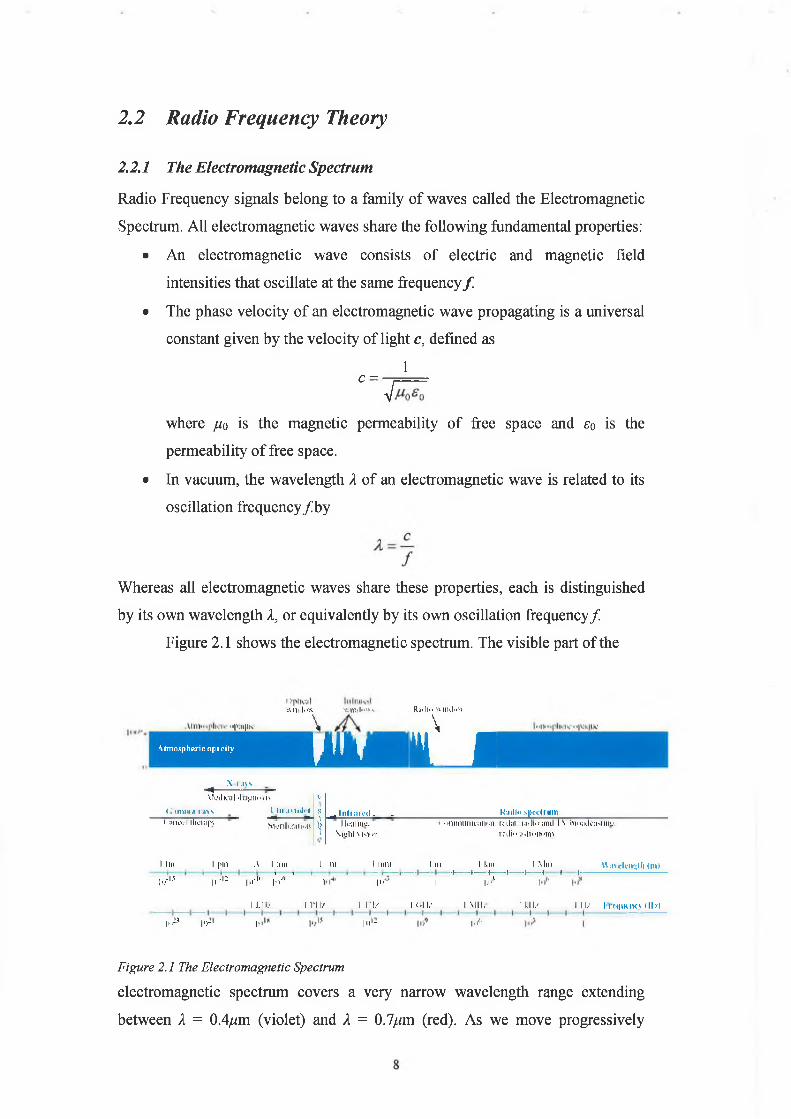
Figure 2.1 shows the electromagnetic spectrum. The visible part of the
"p.h|lk
•A Ill.J.AA\ V. nvl**« •. RaJit* w niil"V, \Atmospheric opacity f 'I T IL 1
XllNN ^ ----- ----MoiJk'iil duiyih'ib V
<¿¡111)111* i»»>\ I III .iM.-I. I s _ 1 nini red _ _ limilo spectrumI nno.-MlkT;i|v> sicnliiCiiiMi i
II Itfllill-J.
\ yj\W \ish»n
i «•mniliimiilMi. rculnr. Tin)i*>nml l\ hi'Milcjsiiiil'
riiili«* :r %lr* «it- »in>
llm 1 pm 1 A I inn [ 111 1 mill i in 1 km • ■ i I Min W ;i\clciiul!i (ill) i i « i i.
I-.»“15 in’12 in '1'■ i > ' Ì 11 • *' i
1 1 T
II'1
i i i i I
11: t 1/ I H 1/ 1 III/ i (til/ 1 M il/ 1 Ml/ 1 11/ lTf<|lklK\ 4IIX»
i.i* i»-1 i* in'- 1‘
Figure 2.1 The Electromagnetic Spectrum
electromagnetic spectrum covers a very narrow wavelength range extending
between A = 0.4/^m (violet) and A = 0.7^m (red). As we move progressively
toward shorter wavelengths, we encounter the ultraviolet, x-ray and gamma-ray
bands, each so named because of historical reasons associated with the discovery
of waves with those wavelengths. On the other side of the visible spectrum lie the
infrared band and then the radio region. Because of the link between X and/ given
above, each of these spectral ranges may be specified in terms of its wavelength
range or alternatively in terms of its frequency range. In practice however, a wave
is specified in terms of its wavelength if X < 1mm, which encompasses all parts of
the electromagnetic spectrum except for the radio region, and the wave is
specified in terms of its frequency / if X > 1mm ( i.e. in the radio region). A
wavelength of 1mm corresponds to a frequency of 3 x 10¹¹ Hz = 300 GHz in free
space.
The radio spectrum consists of several individual bands. Each band covers
one decade of the radio spectrum and has a letter designation based on a
nomenclature defined by the International Telecommunication Union. Different
frequencies have different applications because they are excited by different
mechanisms, and the properties of an electromagnetic wave propagating in a
material may vary considerably from one band to another. The extremely low
frequency (ELF) band from 3 to 30 Hz is used primarily for the detection of
buried metal objects. Lower frequencies down to 0.1 Hz are used in
magnetotelluric sensing of the structure of the earth, and frequencies in the range
from 1 Hz to 1kHz sometimes are used for communications with submerged
submarines and for certain kinds of sensing of Earth’s ionosphere. The very low
frequency (VLF) region from 3 to 30kHz is used both for submarine
communications and for position location by the Omega navigation system. The
low-frequency (LF) band, from 30 to 300 kHz, is used for some forms of
communication and for the Loran C position-location system. Some radio
beacons and weather broadcast stations used in air navigation operate at
frequencies in the higher end of the LF band. The medium-frequency (MF)
region from 300 kHz to 3 MHz contains the standard AM broadcast band from
0.5 to 1.5 MHz.
Long-distance communications and short-wave broadcasting over long
distances use frequencies in the high-frequency (HF) band from 30 MHz because
waves in this band are strongly affected by reflections by the ionosphere and least
9
affected by absorptions in the ionosphere. The next frequency region, the very
high frequency (VHF) band from 30 to 300 MHz, is used for aircraft and other
vehicles. Some early radio-astronomy research was also conducted in this range.
The ultrahigh frequency (UHF) region from 300 MHz to 3 GHz is extensively
populated with radars, although part of this band also is used for television
broadcasting and mobile communications with aircraft and surface vehicles. The
radars in this region of the spectrum are normally used for aircraft detection and
tracking. Some parts of this region have been reserved for radio astronomical
observation.
Many point-to-point radio communication systems and various kinds of
ground-based radars and ship radars operate at frequencies in the super high
frequency (SHF) range from 3 to 30 GHz. Some aircraft navigation systems
operate in this range as well. Most of the extremely high frequency (EHF) band
from 30 to 300 GHz is used less extensively, primarily because the technology is
not as well developed and because of excessive absorption by the atmosphere in
some parts of this band. Some advanced communication systems are being
developed for operation at frequencies in the “atmospheric windows”, where
atmospheric absorption is not a serious problem, as are automobile collision-
avoidance radars and some military imaging radar systems. These atmospheric
windows include the ranges from 30 to 35 GHz, 70 to 75 GHz, 90 to 95 GHz, and
135 to 145 GHz.
The radio frequencies generally used in capacitively coupled plasma
discharge chambers are 2 MHz, 13.56 MHz and 27 MHz. The system developed
for this thesis uses a 13.56 MHz power source. The corresponding wavelength is
X ~ 22.1 metres. There is no particular reason for the use of the HF band of radio
frequencies. It has simply been allocated by the International
Telecommunications Union for use in plasma chamber systems. The power levels
of the signal can range from 0 to 3000 Watts. A range of 0 to 150 Watts is used in
the system developed for this thesis. It is clear that, even in the small window of
the electromagnetic spectrum and power settings, there is a wide range of
conditions that can be used to generate plasmas.
10
2.2.2 Radio Frequency versus DC or Low A C Signals
There are several major differences between signals at higher radio frequency and
there counterparts at low AC frequency or DC. These differences, which greatly
influence electronic circuits and their operation, become increasingly important
as the frequency is raised. The following four effects provide a brief summary of
the effects of radio frequency signals in a circuit that are not present at DC or low
AC signals:
a). Presence o f stray capacitances. This is the capacitance that exists:
b). Presence o f stray inductances. This is the inductance that exists due to:
• The inductance of the conductors that connect components
• The parasitic inductance of the components themselves
These stray parameters are not usually important at DC and low AC frequencies,
but as frequency increases, they become a much larger portion of the total.
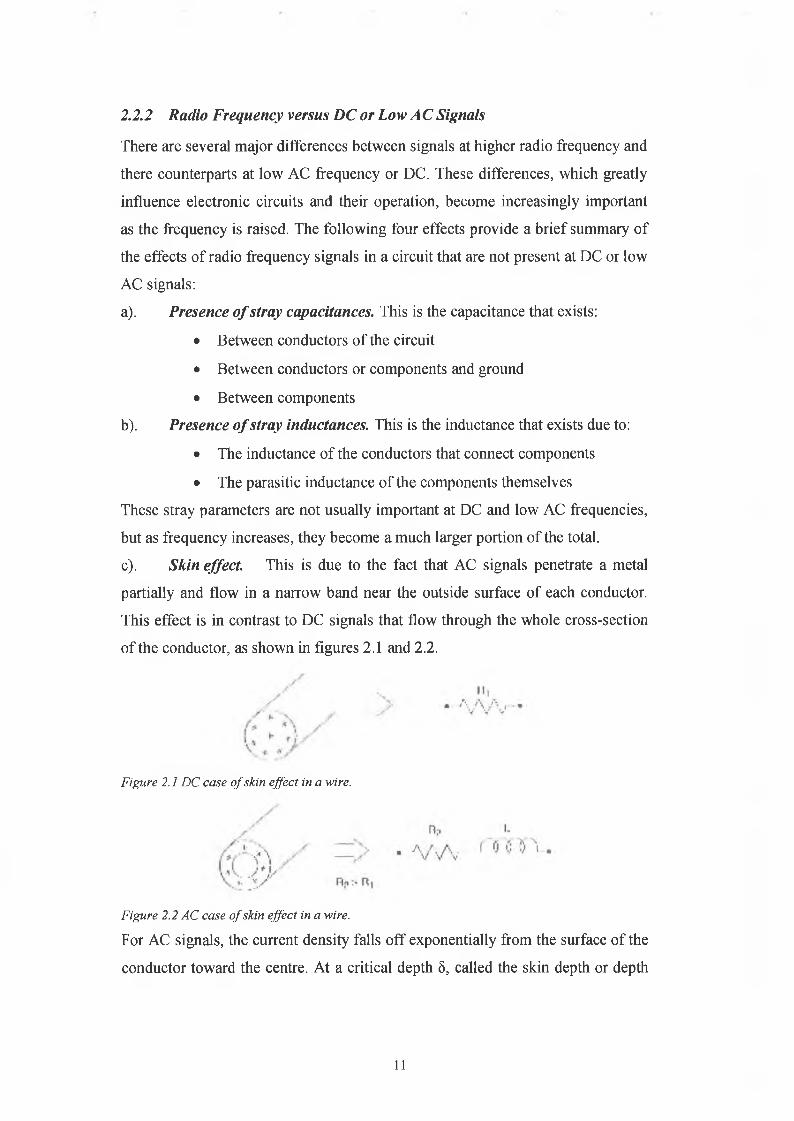
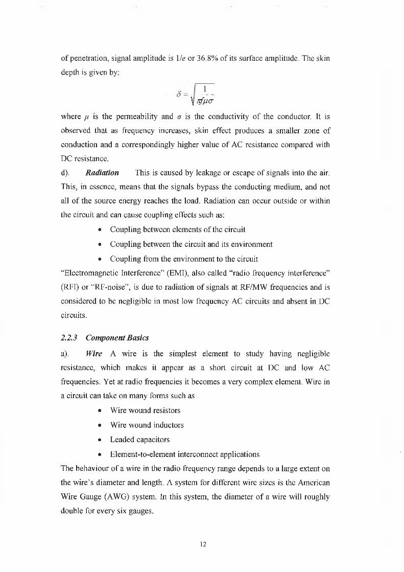
c). Skin effect. This is due to the fact that AC signals penetrate a metal
partially and flow in a narrow band near the outside surface of each conductor.
This effect is in contrast to DC signals that flow through the whole cross-section
of the conductor, as shown in figures 2.1 and 2.2.
Figure 2.1 DC case o f skin effect in a wire.
Figure 2.2 AC case o f skin effect in a wire.
For AC signals, the current density falls off exponentially from the surface of the
conductor toward the centre. At a critical depth 8, called the skin depth or depth
• Between conductors of the circuit
• Between conductors or components and ground
• Between components
11
of penetration, signal amplitude is Me or 36.8% of its surface amplitude. The skin
depth is given by:
$ N o
where f.i is the permeability and a is the conductivity of the conductor. It is
observed that as frequency increases, skin effect produces a smaller zone of
conduction and a correspondingly higher value of AC resistance compared with
DC resistance.
d). Radiation This is caused by leakage or escape of signals into the air.
This, in essence, means that the signals bypass the conducting medium, and not
all of the source energy reaches the load. Radiation can occur outside or within
the circuit and can cause coupling effects such as:
• Coupling between elements of the circuit
• Coupling between the circuit and its environment
• Coupling from the environment to the circuit
“Electromagnetic Interference” (EMI), also called “radio frequency interference”
(RFI) or “RF-noise”, is due to radiation of signals at RF/MW frequencies and is
considered to be negligible in most low frequency AC circuits and absent in DC
circuits.
2.2.3 Component Basics
a). Wire A wire is the simplest element to study having negligible
resistance, which makes it appear as a short circuit at DC and low AC
frequencies. Yet at radio frequencies it becomes a very complex element. Wire in
a circuit can take on many forms such as
• Wire wound resistors
• Wire wound inductors
• Leaded capacitors
• Element-to-element interconnect applications
The behaviour of a wire in the radio frequency range depends to a large extent on
the wire’s diameter and length. A system for different wire sizes is the American
Wire Gauge (AWG) system. In this system, the diameter of a wire will roughly
double for every six gauges.
12
Problems associated with a wire can be traced to two areas: skin effect
and straight-wire inductance. As frequency increases, the electrical signals
propagate less and less in the inside of the conductor. The current density
increases near the outside perimeter of the wire and causes a higher impedance to
be seen by the signal. This is because resistance of the wire is given by:
r = £A
and if the effective area, A, decreases, this leads to an increase in resistance, R.
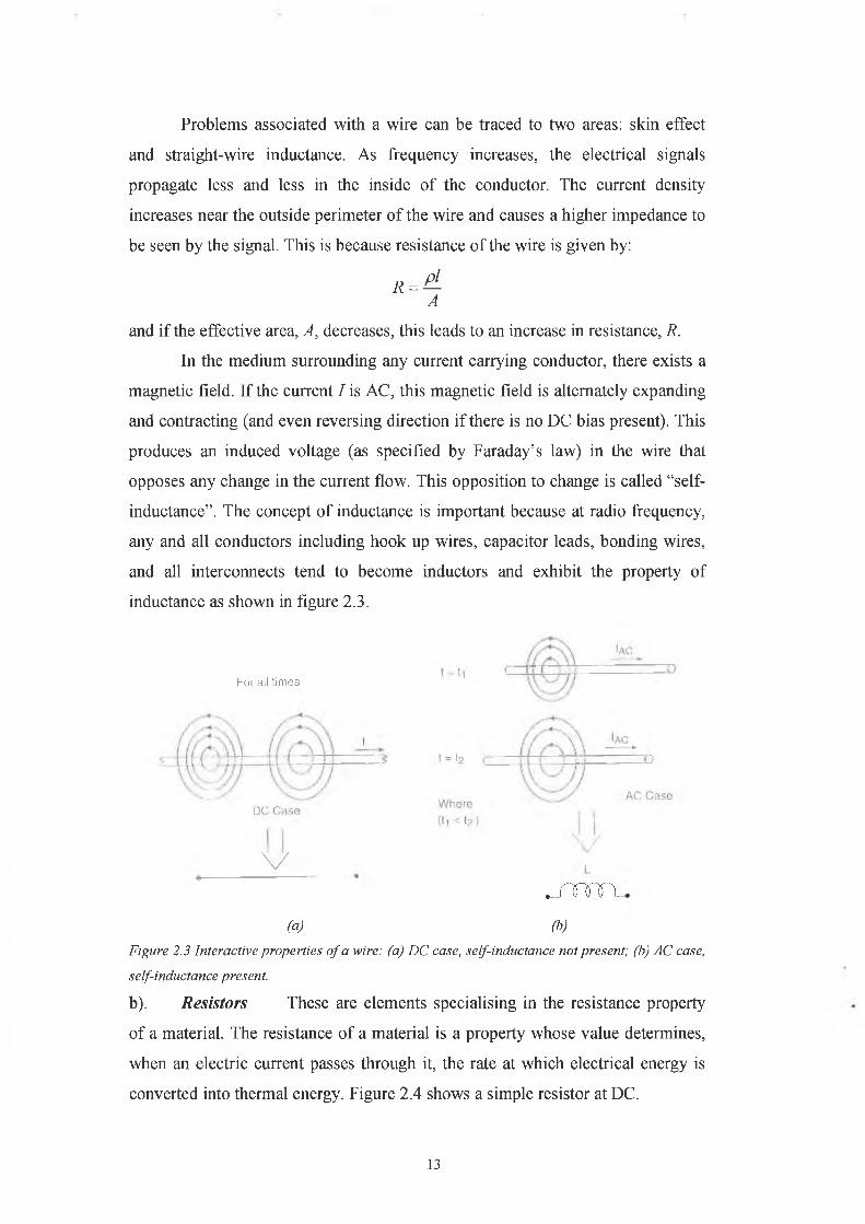
In the medium surrounding any current carrying conductor, there exists a
magnetic field. If the current / is AC, this magnetic field is alternately expanding
and contracting (and even reversing direction if there is no DC bias present). This
produces an induced voltage (as specified by Faraday’s law) in the wire that
opposes any change in the current flow. This opposition to change is called “self
inductance”. The concept of inductance is important because at radio frequency,
any and all conductors including hook up wires, capacitor leads, bonding wires,
and all interconnects tend to become inductors and exhibit the property of
inductance as shown in figure 2.3.
Foi all tim es
V
(a)
^ / r m
(b)
Figure 2.3 Interactive properties o f a wire: (a) DC case, self-inductance not present; (b) AC case,
self-inductance present.
b). Resistors These are elements specialising in the resistance property
of a material. The resistance of a material is a property whose value determines,
when an electric current passes through it, the rate at which electrical energy is
converted into thermal energy. Figure 2.4 shows a simple resistor at DC.
13
R L R ' L
•— m — • = >( At DC )
(a) ----------------------------- 1 j----------------------------C
( A t R F )
Figure 2.4 A simple resistor at (a) DC, (b) high RF frequency.
As frequency increases, the lead wire inductance (X), increased resistor value
(R ’>R) due to skin effect and parasitic capacitances becomes prominent. The net
effect of all these parasitic elements, on the average, is a decrease in the resistor
value as for carbon-composition and metal resistors. Therefore, at radio
frequency, a resistor appears as a combination of several elements,
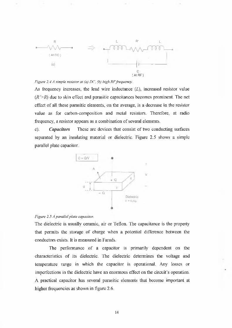
c). Capacitors These are devices that consist of two conducting surfaces
separated by an insulating material or dielectric. Figure 2.5 shows a simple
parallel plate capacitor.
Figure 2.5 A parallel plate capacitor.
The dielectric is usually ceramic, air or Teflon. The capacitance is the property
that permits the storage of charge when a potential difference between the
conductors exists. It is measured in Farads.
The performance of a capacitor is primarily dependent on the
characteristics of its dielectric. The dielectric determines the voltage and
temperature range in which the capacitor is operational. Any losses or
imperfections in the dielectric have an enormous effect on the circuit’s operation.
A practical capacitor has several parasitic elements that become important at
higher frequencies as shown in figure 2.6.
14
+ 1 Rs — v w —
+
Capacitori
u o o r L / v w
--------------l i -------------
c
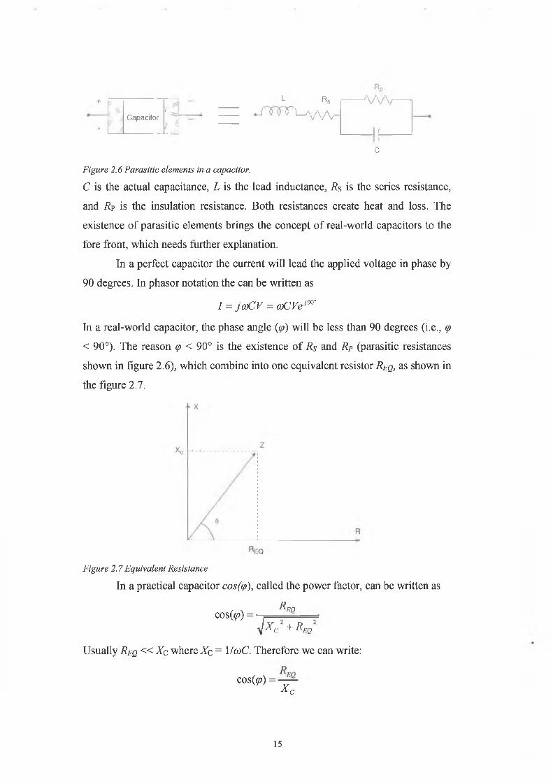
Figure 2.6 Parasitic elements in a capacitor.
C is the actual capacitance, L is the lead inductance, Rs is the series resistance,
and Rp is the insulation resistance. Both resistances create heat and loss. The
existence of parasitic elements brings the concept of real-world capacitors to the
fore front, which needs further explanation.
In a perfect capacitor the current will lead the applied voltage in phase by
90 degrees. In phasor notation the can be written as
I = jcoCV = coCVej90°
In a real-world capacitor, the phase angle (<p) will be less than 90 degrees (i.e., (p
< 90°). The reason (p < 90° is the existence of R s and R p (parasitic resistances
shown in figure 2.6), which combine into one equivalent resistor R e q , as shown in
the figure 2.7.
Figure 2.7 Equivalent Resistance
In a practical capacitor cos(cp), called the power factor, can be written as
Rpocos (<p) = ~r - ■
4 x c + r eq
Usually Req « Xc where Xc = HcoC. Therefore we can write:
cos (<p) = ——X c
15
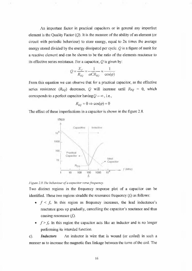
An important factor in practical capacitors or in general any imperfect
element is the Quality Factor (Q). It is the measure of the ability of an element (or
circuit with periodic behaviour) to store energy, equal to 2n times the average
energy stored divided by the energy dissipated per cycle. Q is a figure of merit for
a reactive element and can be shown to be the ratio of the elements reactance to
its effective series resistance. For a capacitor, Q is given by:
REQ coCReq cos {(p)
From this equation we can observe that for a practical capacitor, as the effective
series resistance (R eq) decreases, Q will increase until R eq - 0, which
corresponds to a perfect capacitor havingQ - oo, i.e.,
r eq = 0 => cos(#)) = 0
The effect of these imperfections in a capacitor is shown in the figure 2.8.
IZ I(Q )
Figure 2.8 The behaviour o f a capacitor verus frequency.
Two distinct regions in the frequency response plot of a capacitor can be
identified. These two regions straddle the resonance frequency (fT) as follows:
• / < f T. In this region as frequency increases, the lead inductance’s
reactance goes up gradually, cancelling the capacitor’s reactance and thus
causing resonance (fr).
• f > f T. In this region the capacitor acts like an inductor and is no longer
performing its intended function.
c). Inductors An inductor is wire that is wound (or coiled) in such a
manner as to increase the magnetic flux linkage between the turns of the coil. The
16
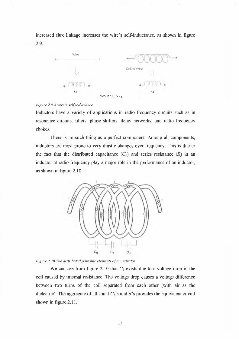
increased flux linkage increases the wire’s self-inductance, as shown in figure
Wire
Coiied Wire
V i}
Li L2Result : L2 > L!
Figure 2.9 A wire's self inductance.
Inductors have a variety of applications in radio frequency circuits such as in
resonance circuits, filters, phase shifters, delay networks, and radio frequency
chokes.
There is no such thing as a perfect component. Among all components,
inductors are most prone to very drastic changes over frequency. This is due to
the fact that the distributed capacitance (Cd) and series resistance (R) in an
inductor at radio frequency play a major role in the performance of an inductor,
as shown in figure 2.10.
Figure 2.10 The distributed parasitic elements o f an inductor
We can see from figure 2.10 that Cd exists due to a voltage drop in the
coil caused by internal resistance. The voltage drop causes a voltage difference
between two turns of the coil separated from each other (with air as the
dielectric). The aggregate of all small Cd’s and R’s provides the equivalent circuit
shown in figure 2.11.
17
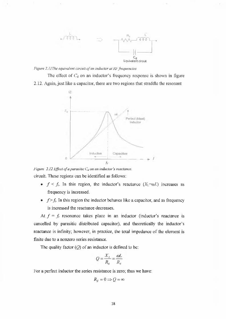
=>Rs L
A A A r - ^ ^ V
*Cd
Equivalent circuit
Figure 2.1 ¡The equivalent circuit o f an inductor at RFfrequencies
The effect of Cd on an inductor’s frequency response is shown in figure
2.12. Again Just like a capacitor, there are two regions that straddle the resonant
IZI
Figure 2.12 Effect o f a parasitic Cj on an inductor's reactance.
circuit. These regions can be identified as follows:
• f < ft. In this region, the inductor’s reactance (Ax=©I) increases as
frequency is increased.
• / > f T. In this region the inductor behaves like a capacitor, and as frequency
is increased the reactance decreases.
At / = f resonance takes place in an inductor (inductor’s reactance is
cancelled by parasitic distributed capacitor), and theoretically the inductor’s
reactance is infinity; however, in practice, the total impedance of the element is
finite due to a nonzero series resistance.
The quality factor (Q) of an inductor is defined to be:
Q — L - .
Rs Rs
For a perfect inductor the series resistance is zero; thus we have:
Rs = 0 => Q = oo
18
At low frequencies, Q is very large because Rs is very small; however, as
frequency increases the skin effect and winding distributed capacitor (Cd) begin
to degrade the Q of an inductor as shown in figure 2.13.
Q
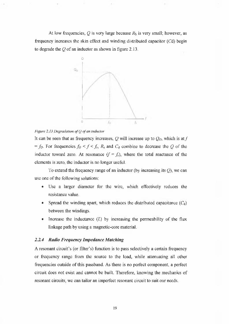
Figure 2.13 Degradation o f Q o f an inductor
It can be seen that as frequency increases, Q will increase up to Qo, which is at/
= fo. For frequencies fo < f < fr, Rs and Cd combine to decrease the Q of the
inductor toward zero. At resonance (f = f ) , where the total reactance of the
elements is zero, the inductor is no longer useful.
To extend the frequency range of an inductor (by increasing its Q), we can
use one of the following solutions:
• Use a larger diameter for the wire, which effectively reduces the
resistance value.
• Spread the winding apart, which reduces the distributed capacitance (Cd)
between the windings.
• Increase the inductance (L) by increasing the permeability of the flux
linkage path by using a magnetic-core material.
2.2.4 Radio Frequency Impedance Matching
A resonant circuit’s (or filter’s) function is to pass selectively a certain frequency
or frequency range from the source to the load, while attenuating all other
frequencies outside of this passband. As there is no perfect component, a perfect
circuit does not exist and cannot be built. Therefore, knowing the mechanics of
resonant circuits, we can tailor an imperfect resonant circuit to suit our needs.
19
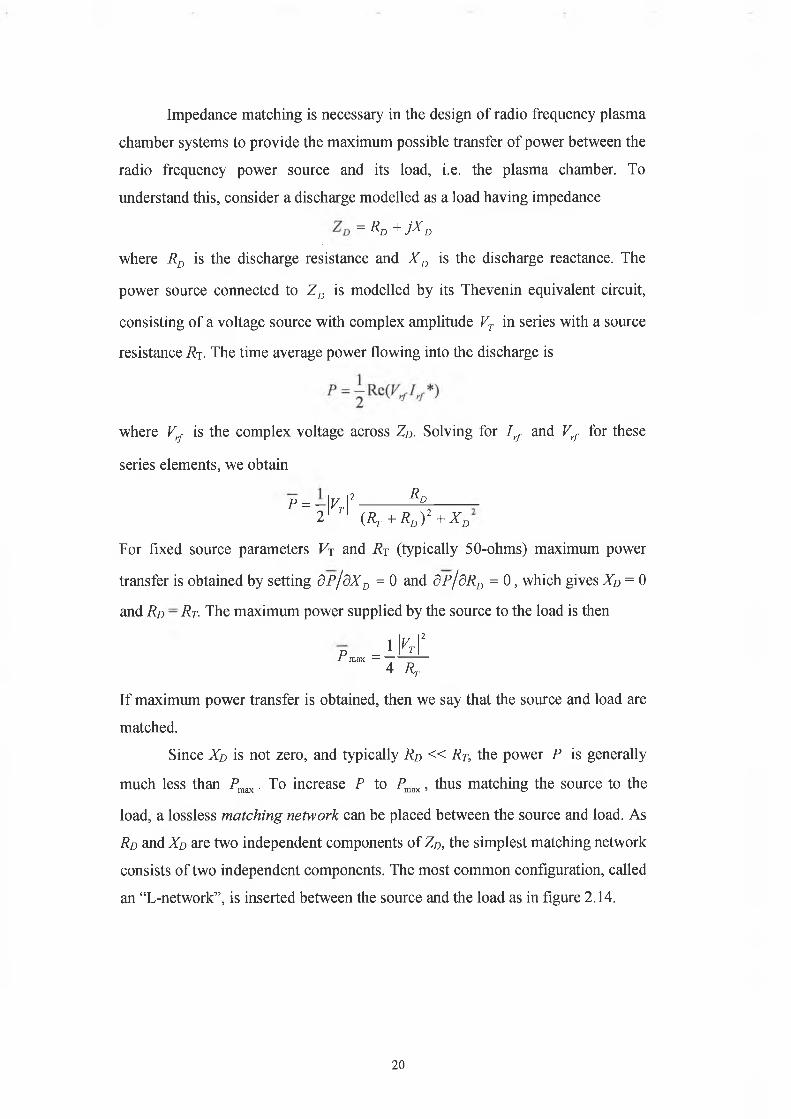
Impedance matching is necessary in the design of radio frequency plasma
chamber systems to provide the maximum possible transfer of power between the
radio frequency power source and its load, i.e. the plasma chamber. To
understand this, consider a discharge modelled as a load having impedance
= Rd + jX D
where RD is the discharge resistance and X D is the discharge reactance. The
power source connected to ZD is modelled by its Thevenin equivalent circuit,
consisting of a voltage source with complex amplitude VT in series with a source
resistance Rj. The time average power flowing into the discharge is
where Vrf is the complex voltage across Zn. Solving for Irf and Vrf for these
series elements, we obtain
P = -\V T |2--------- \ ---------2 CRt + Rd)2 + X d
For fixed source parameters Vj and Rj (typically 50-ohms) maximum power
transfer is obtained by setting dP/dXD = 0 and dP/dRD = 0 , which gives XD = 0
and Rp - Rt■ The maximum power supplied by the source to the load is then
p _ i Kfr max —
4 Rt
If maximum power transfer is obtained, then we say that the source and load are
matched.
Since XD is not zero, and typically Rd « Rt, the power P is generally
much less than Pmax. To increase P to PnrdX, thus matching the source to the
load, a lossless matching network can be placed between the source and load. As
Rd and XD are two independent components of Zn, the simplest matching network
consists of two independent components. The most common configuration, called
an “L-network”, is inserted between the source and the load as in figure 2.14.
20
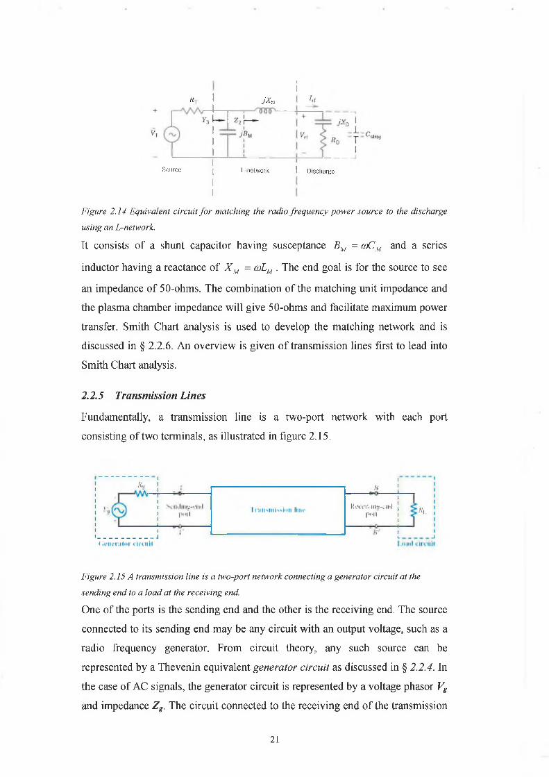
I
i« r 1 JXw,
Source | L-ietwor'< 1 Disc large
Figure 2.14 Equivalent circuit fo r matching the radio frequency power source to the discharge
using an L-network.
It consists of a shunt capacitor having susceptance Bu = coCM and a series
inductor having a reactance of X M - a>LM . The end goal is for the source to see
an impedance of 50-ohms. The combination of the matching unit impedance and
the plasma chamber impedance will give 50-ohms and facilitate maximum power
transfer. Smith Chart analysis is used to develop the matching network and is
discussed in § 2.2.6. An overview is given of transmission lines first to lead into
Smith Chart analysis.
2.2.5 Transmission Lines
Fundamentally, a transmission line is a two-port network with each port
consisting of two terminals, as illustrated in figure 2.15.
Figure 2.15 A transmission line is a two-port network connecting a generator circuit at the
sending end to a load at the receiving end.
One of the ports is the sending end and the other is the receiving end. The source
connected to its sending end may be any circuit with an output voltage, such as a
radio frequency generator. From circuit theory, any such source can be
represented by a Thevenin equivalent generator circuit as discussed in § 2.2.4. In
the case of AC signals, the generator circuit is represented by a voltage phasor Vg
and impedance Zg. The circuit connected to the receiving end of the transmission
21
line is called the load circuit, or simply the load. This will be the capacitively
coupled plasma chamber and is represented by an equivalent load resistance Rl or
a load impedance Zl in the AC case.
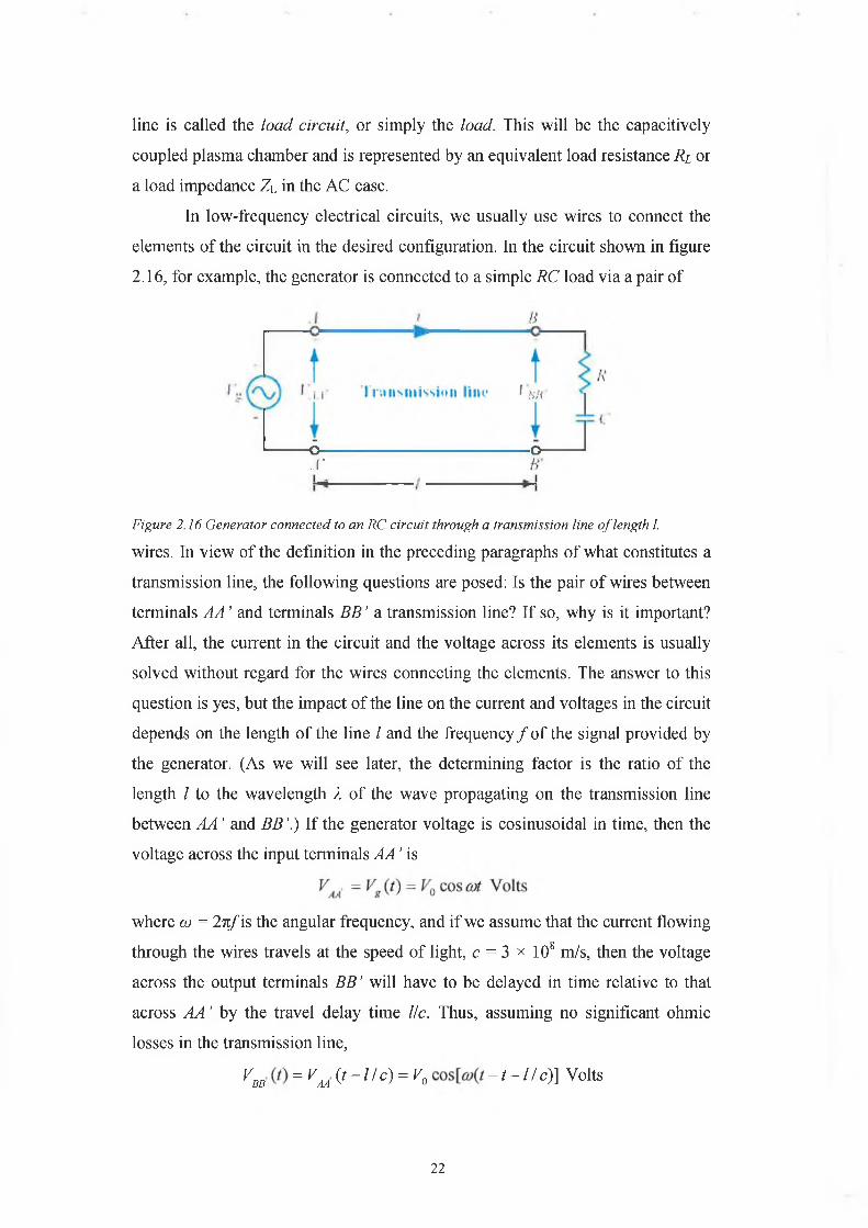
In low-frequency electrical circuits, we usually use wires to connect the
elements of the circuit in the desired configuration. In the circuit shown in figure
2.16, for example, the generator is connected to a simple RC load via a pair of
Figure 2.16 Generator connected to an RC circuit through a transmission line o f length I.
wires. In view of the definition in the preceding paragraphs of what constitutes a
transmission line, the following questions are posed: Is the pair of wires between
terminals AA ’ and terminals BB ’ a transmission line? If so, why is it important?
After all, the current in the circuit and the voltage across its elements is usually
solved without regard for the wires connecting the elements. The answer to this
question is yes, but the impact of the line on the current and voltages in the circuit
depends on the length of the line / and the frequency / of the signal provided by
the generator. (As we will see later, the determining factor is the ratio of the
length I to the wavelength X of the wave propagating on the transmission line
between AA ’ and BB ’.) If the generator voltage is cosinusoidal in time, then the
voltage across the input terminals AA ’ is
where co = 2nfis the angular frequency, and if we assume that the current flowing
through the wires travels at the speed of light, c = 3 x 10⁸ m/s, then the voltage
across the output terminals BB ’ will have to be delayed in time relative to that
across AA ’ by the travel delay time He. Thus, assuming no significant ohmic
losses in the transmission line,
o -.r
o
VBB = VAA^~llC = V0 - t - l / c ) ] Volts
22
Let us compare Vb b - to Va a - at t = 0 for an ultralow-frequency electronic circuit
operating at a frequency/ = 1 kHz. For a typical wire length I = 5cm, the above
equations give Vaa' = Vo and Vaa - = V0 cos(2nfl/c) = 0.999999999998 V0. Thus,
for all practical purposes, the length of the transmission line may be ignored and
terminal AA ’ may be treated as identical to BB ’. On the other hand, had the line
been 20km long telephone cable carrying a 1 kHz voice signal, then the same
calculation would have led to Vb b - = 0.91 Vo. The determining factor is the
magnitude of col/c. The velocity of propagation up of a travelling wave is related
to the oscillation frequency/ and the wavelength X by
up = fX m/s
In the present case, up = c. Hence, the phase factor
0)1 27lfl . I— = —— = 2 n — radiansc c X
When l/X is very small, transmission-line effects may be ignored, but when l/X >
0.01, it may be necessary to account not only for the phase shift associated with
the time delay, but also for the presence of reflected signals that may have been
bounced back by the load toward the generator. Power loss on the line and
dispersive effects may need to be considered as well. A dispersive transmission
line is one on which the wave velocity is not constant as a function of the
frequency f. This means that the shape of a rectangular pulse, which through
Fourier analysis is composed of many waves of different frequencies, will be
distorted as it travels down the line because its different frequency components
will not propagate at the same velocity. The relevance of these factors to the
design of plasma chambers may be important when the distance between the
power generator and plasma chamber is large, for example if the power generator
is in the “sub-fab” area of a semiconductor fabrication factory.
2.2.5.2 Propagation Modes
Transmission lines may be classified into two basic types:
Transverse electromagnetic (TEM) transmission lines: Waves propagating
along these lines are characterised by electric and magnetic fields that are entirely
transverse to the direction of propagation. This is called a TEM mode. A good
example is the coaxial load shown in figure 2.17; the electric field lines are in the
23
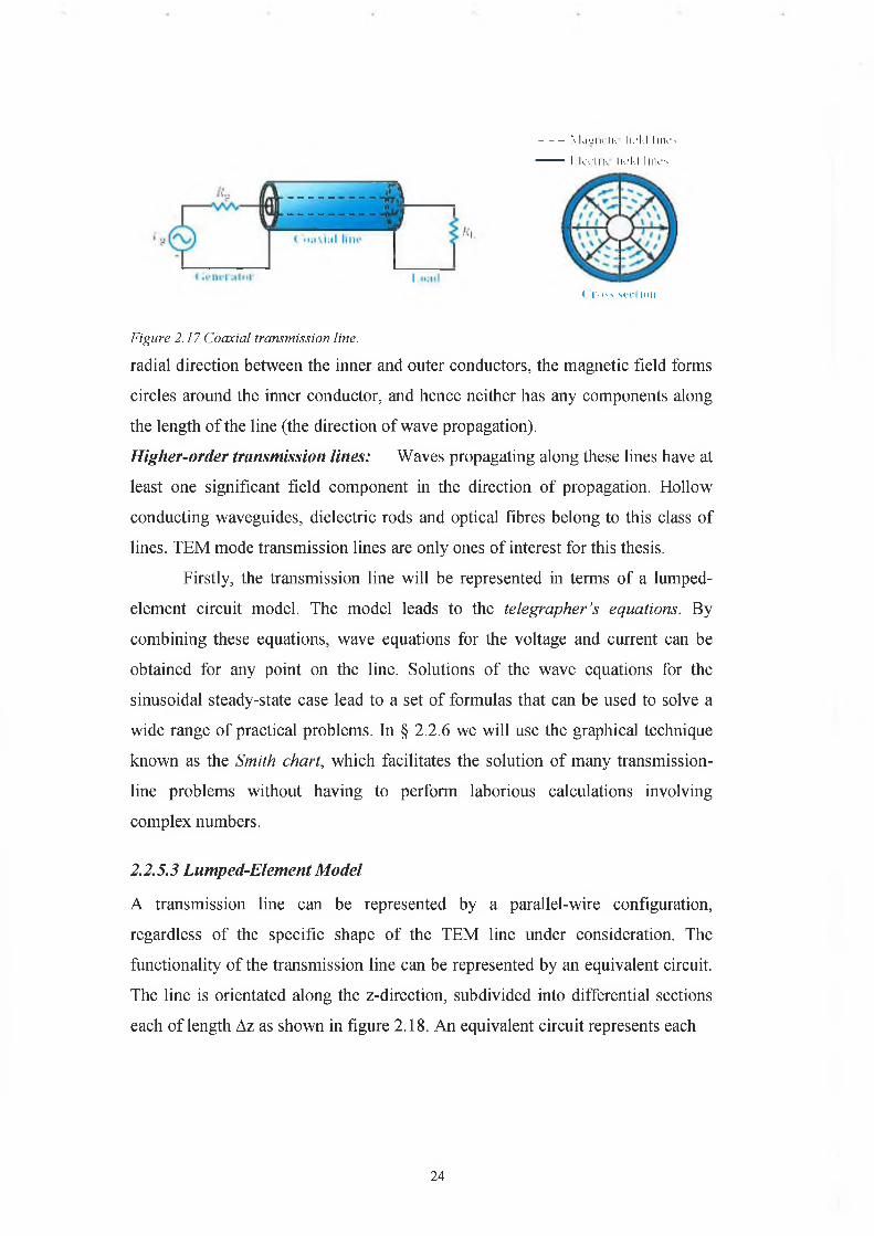
-------- M , l '- H k lk Ik 'k l I UK's
--------- I k v l l l ' . Ik 'k l l l lk 's
< r i >s\ s r d in n
Figure 2.17 Coaxial transmission line.
radial direction between the inner and outer conductors, the magnetic field forms
circles around the inner conductor, and hence neither has any components along
the length of the line (the direction of wave propagation).
Higher-order transmission lines: Waves propagating along these lines have at
least one significant field component in the direction of propagation. Hollow
conducting waveguides, dielectric rods and optical fibres belong to this class of
lines. TEM mode transmission lines are only ones of interest for this thesis.
Firstly, the transmission line will be represented in terms of a lumped-
element circuit model. The model leads to the telegrapher’s equations. By
combining these equations, wave equations for the voltage and current can be
obtained for any point on the line. Solutions of the wave equations for the
sinusoidal steady-state case lead to a set of formulas that can be used to solve a
wide range of practical problems. In § 2.2.6 we will use the graphical technique
known as the Smith chart, which facilitates the solution of many transmission-
line problems without having to perform laborious calculations involving
complex numbers.
2.2.53 Lumped-Element Model
A transmission line can be represented by a parallel-wire configuration,
regardless of the specific shape of the TEM line under consideration. The
functionality of the transmission line can be represented by an equivalent circuit.
The line is orientated along the z-direction, subdivided into differential sections
each of length Az as shown in figure 2.18. An equivalent circuit represents each
24
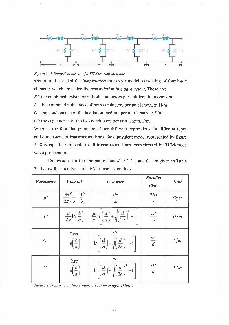
■►H---------- :------- ►+<--------- :-------- *+«--------- :-------- H
Figure 2.18 Equivalent circuit o f a TEM transmission line.
section and is called the lumped-element circuit model, consisting of four basic
elements which are called the transmission line parameters. These are:
R ’: the combined resistance of both conductors per unit length, in ohms/m,
L ’: the combined inductance of both conductors per unit length, in H/m
G ’: the conductance of the insulation medium per unit length, in S/m
C ’: the capacitance of the two conductors per unit length, F/m
Whereas the four line parameters have different expressions for different types
and dimensions of transmission lines, the equivalent model represented by figure
2.18 is equally applicable to all transmission lines characterised by TEM-mode
wave propagation.
Expressions for the line parameters R \L \ G ’, and C ’ are given in Table
2.1 below for three types of TEM transmission lines.
Parameter Coaxial Two wireParallel
PlateUnit
R ’R s i l + l^ 2 n \a b)
Rsm
2 Rs w
Cl/m
L ’ — 4-Ì2 n ya )—Inn V«ry Vv2 a )
/.jd w
H/m
G ’2na no
ow~d
S/mInV
In d '.a , +Jy2a)
2-1
C ’2ns ne
ew~d
F/mInU J
In 'd'. a )+i( d
\ 2 a )
2-1
Table 2.1 Transmission-line parameters fo r three types o f lines.
25
The expressions are functions of two sets of parameters: (1) geometric parameters
defining the cross-sectional dimensions of the given line and (2) electromagnetic
constitutive parameters characteristic of the materials of which the conductors
and the insulating material between them are made. The pertinent geometric
parameters are as follows:
Coaxial line
• a = outer radius of inner conductor
• b = inner radius of outer conductor
Two-wire line
• a = radius of each wire
• d = spacing between wire’s centres
Parallel-plate line
• w = width of each plate
• d = thickness of insulation between plates
The constitutive parameters apply to all three lines and consist of two groups: /¿c
and <7C are the magnetic permeability and electrical conductivity of the
conductors, and e, // and a are the electrical permittivity, magnetic permeability,
and electrical conductivity of the insulation material separating the conductors.
The lumped-element model represents the physical processes associated
with the currents and voltages on any TEM transmission line. The model (shown
in figure 2.18 above) leads to a set of equations called the telegrapher’s
equations. It consists of two series elements, R ’ and L ’, and two shunt elements,
G ’ and C ’. By way of providing a physical explanation for the lumped-element
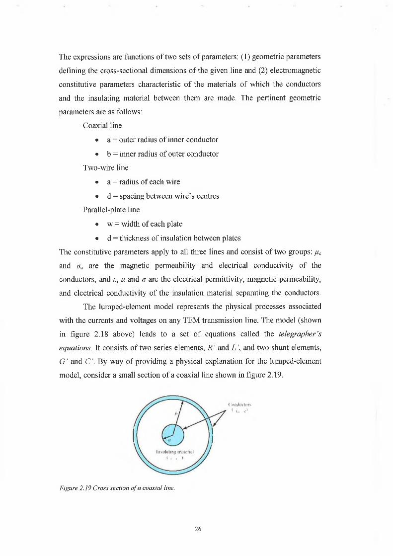
model, consider a small section of a coaxial line shown in figure 2.19.
Figure 2.19 Cross section o f a coaxial line.
26
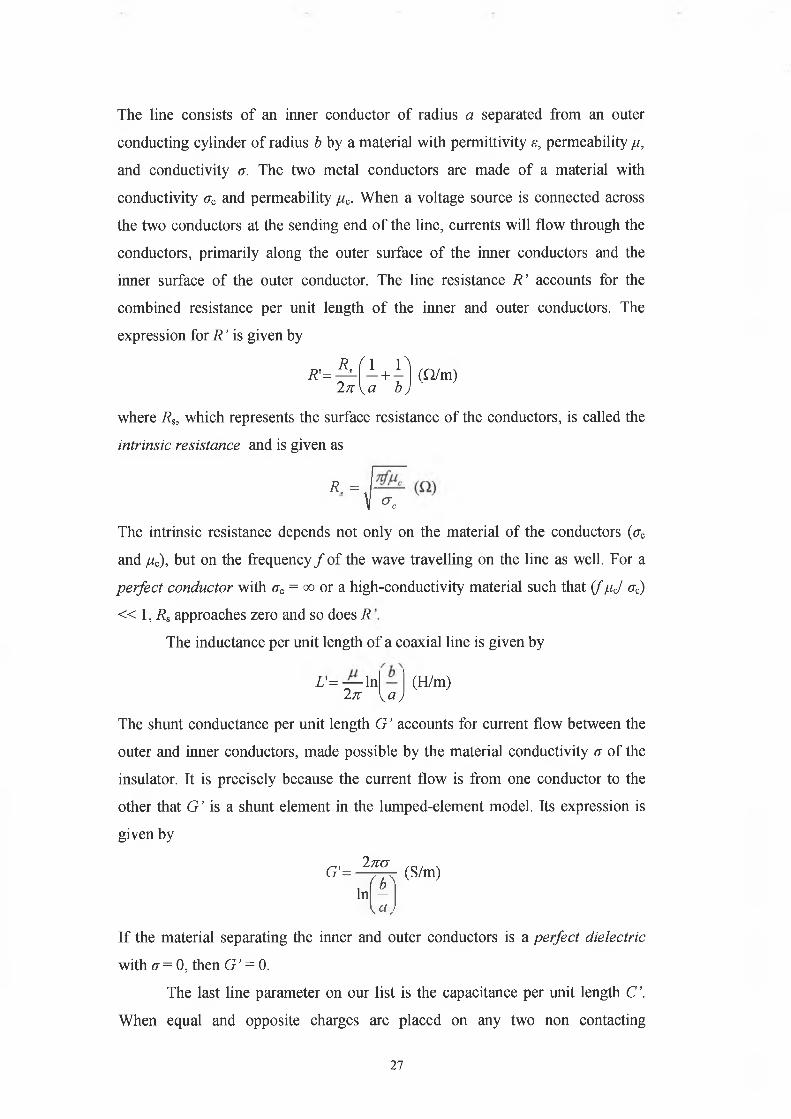
The line consists of an inner conductor of radius a separated from an outer
conducting cylinder of radius b by a material with permittivity e, permeability /.i,
and conductivity a. The two metal conductors are made of a material with
conductivity ac and permeability fic. When a voltage source is connected across
the two conductors at the sending end of the line, currents will flow through the
conductors, primarily along the outer surface of the inner conductors and the
inner surface of the outer conductor. The line resistance R ’ accounts for the
combined resistance per unit length of the inner and outer conductors. The
expression for R ’ is given by
R (1 n R'=-^~ - + - (H/m)
2 n \ a b)
where Rs, which represents the surface resistance of the conductors, is called the
intrinsic resistance and is given as
R. =V ^
The intrinsic resistance depends not only on the material of the conductors (<rc
and /4C), but on the frequency / of the wave travelling on the line as well. For a
perfect conductor with az = oo or a high-conductivity material such that i f ¡.ij ac)
<<1 , RS approaches zero and so does R
The inductance per unit length of a coaxial line is given by
L'= — In2 n \ a )
(H/m)
The shunt conductance per unit length G ’ accounts for current flow between the
outer and inner conductors, made possible by the material conductivity a of the
insulator. It is precisely because the current flow is from one conductor to the
other that G ’ is a shunt element in the lumped-element model. Its expression is
given by
G'=S (S/m)u ,
If the material separating the inner and outer conductors is a perfect dielectric
with <7 = 0, then G ’ = 0.
The last line parameter on our list is the capacitance per unit length C ’.
When equal and opposite charges are placed on any two non contacting
27
c ' = - n ^ (F/m)In
conductors, a voltage difference will be induced between them. Capacitance is
defined as the ratio of charge to voltage difference. For the coaxial line, C ’ is
given by
2ns
\ a j
All TEM transmission lines share the following useful relations:
L'C=f i s
9 L - ZC ' ~ ~ P
2.2.5.4 Transmission Line Equations
A transmission line usually connects a source on one end to a load on the other
end. Equations have been developed that describe the voltage across the
transmission line and the current carried by the line as a function of time t and
spatial position z. These equations are known as the telegrapher’s equations:
Equation 1: - — = (R'+jcoL')I (z)dz
Equation 2: - = (G'+jajC')V(z)dz
Equation 1 and equation 2 are first-order coupled equations and can be combined
to give two second-order uncoupled wave equations, one for V(z) and one for
7(z).
Equation 3: ^ = ^
Equation 4: ^ - y 21 (z) = 0
where
y = J{R'+j(oL'\G'+jcoC')
Equations 3 and 4 are called wave equations for V (z) and I (z), and y is called
the complex propagation constant of the transmission line, y consists of a real
part a, called the attenuation constant of the line with the units of Np/m, and an
28
imaginary part /?, called the phase constant of the line with units of the line with
units of rad/m. Therefore,
y = a + 0
with
a = Re(r ) = Rc(j{R'+jcoL%G'+jcoC'))
P = Im(r ) = Im (j(R'+j<aL%G'+j<oC'))
Equations 3 and 4, the wave equations, have travelling wave solutions of
the following form:
Equation 5: V(z)= V0+e~* + V0~e* Volts
Equation 6: I (z) = I0+e + I0~e* Amps
where the e~yz term represents wave propagation in the + z-direction and the eyz
term represents wave propagation in the - z-direction. There are four unknowns
in these solutions, VQ+ and Ia+ propagating in the + z-direction, V~ and 1~
propagating in the - z-direction. The current wave amplitudes IQ+ and Ia~ can be
related to the voltage wave amplitudes VQ+ and V~ by using equation 5 in
equation 1 and then solving for the current 1 (z) to get the result
l { z ) = r V0' e - v - V - e *R'+jcoV
Comparison of each term with the corresponding term in the expression given by
equation 6 leads to the conclusion that
V + - Vy o _ 7 _ y o AI + -o-*0 -‘o
where
v K+jeoL' \R'+j(oL' ^- I
y V G'+jcoC'
is defined as the characteristic impedance of the line. It should be noted that Z0
is equal to the ratio of the voltage amplitude to the current amplitude for each of
the travelling waves individually (with an additional minus sign in the case of the
-z propagating wave), but it is not equal to the ratio of the total voltage V(z) to
29
the total current / (z), unless one of the two waves is absent. The equation for
I (z) can be rewritten as
Equation7: I(z) = ^ - e * - ^ - e *Z0
Expressions for the wave amplitudes VQ+ and Vo can be found by applying
boundary conditions to the load and sending end of the transmission line. In
general, each will be a complex quantity composed of a magnitude and a phase
angle. Thus
Upon substituting these definitions into Equation 5 and replacing y with
y = a + p , we can convert back to the time domain to obtain an expression for
v{z,t), the instantaneous voltage on the line:
The first term in the above equation is a wave travelling in the + z-direction (as
the coefficients of t and z have opposite signs) and the second term as a wave
travelling in the - z-direction (the coefficients of t and z are both positive), both
propagating with a phase velocity up given by
„ co u „ = = —
p P
The factor e~m accounts for the attenuation of the +z propagating wave and the
e+az accounts for the attenuation of the -z propagating wave. The presence of
two waves on the line propagating in opposite directions produces a standing
wave. To gain a physical understanding of what this means an examination of the
lossless line (a = 0) is required. The results of this examination can be extended
to the lossy transmission line (a * 0) .
2.2.5.5 The Lossless Transmission Line
As has been shown, a transmission line is characterised by two fundamental
properties, its propagation constant y and its characteristic impedance Z0, both
Equation 8: v(z, t) = V 0* e az cos [at - Pz + <fi+)+ \Vo
30
of which are specified by the angular frequency m and the line parameters
R',L',G' and C'. In many practical situations the transmission line can be
designed to minimise ohmic losses by selecting conductors with very high
conductivities and dielectric materials (separating the conductors) with negligible
conductivities. As a result R' and G' assume very small values such that
R'«coL' and G « c o C . These lossless-line conditions allow R = G = 0,
resulting in
Y = a + j f i - jco^L'C'
which means that
a = 0 (lossless line)
P = coyjL'C' (lossless line).
Application of the lossless-line conditions gives the characteristic impedance
[JJZ° = J — (lossless-line)
which is now a real number. Using the lossless expression for jB, the following
relations for the wavelength A and the phase u are obtained:
. _ 2 n _ 2n~ P ~ COyfUC
a) 1U n = — = — r ^ = .p p 4uc
Applying these relationships to L'C'= pie results in
P = coj/jis
1u — .p /
where ¡i and e are the magnetic permeability and electrical permittivity of the
insulating material separating the conductors. Materials used for this purpose are
usually characterised by the permeability /y = //0, where ju(] =4;rxlO“7H/m is
the permeability of free space, and the permittivity is usually specified in terms of
the relative permittivity s r
e
31
where s 0 = 8.854 x 10 12 F/m is the permittivity of free space. Hence
1 1 1
where c = \j /u0£{} =3 x 1 0 %ml s is the velocity of light in a vacuum. If the
insulating material between the conductors is air, then s r = 1 and up - c .
Therefore, given the relationship between X and up
2 = Up = C 1 -
where X0 = c / f is the wavelength in air corresponding to a frequency / . It
should be noted that, because both up and X depend on er, the choice of the
type of insulating material used in a transmission line is dictated not only by its
mechanical properties, but by its electrical properties as well.
When the phase velocity of a medium is independent of frequency, the
medium is called nondispersive, which clearly is the case for a lossless TEM
transmission line. This is an important feature for the transmission of digital data
in the form of pulses. A rectangular pulse or a series of pulses is composed of
many Fourier components with different frequencies. If the phase velocity is the
same for all frequency components (or at least for the dominant ones), the pulse
shape will remain the same as the pulse propagating in a dispersive medium gets
progressively distorted, and the pulse length increases (stretches out) as a
function of distance in the medium, thereby imposing a limitation on the
maximum data rate (which is related to the length of the individual pulses and the
spacing between adjacent pulses) that can be transmitted through the medium
without loss of information.
Table 2.2 provides a list of expressions for y , Z0 and up for the general
case of a lossy line and for several types of lossless lines.
32
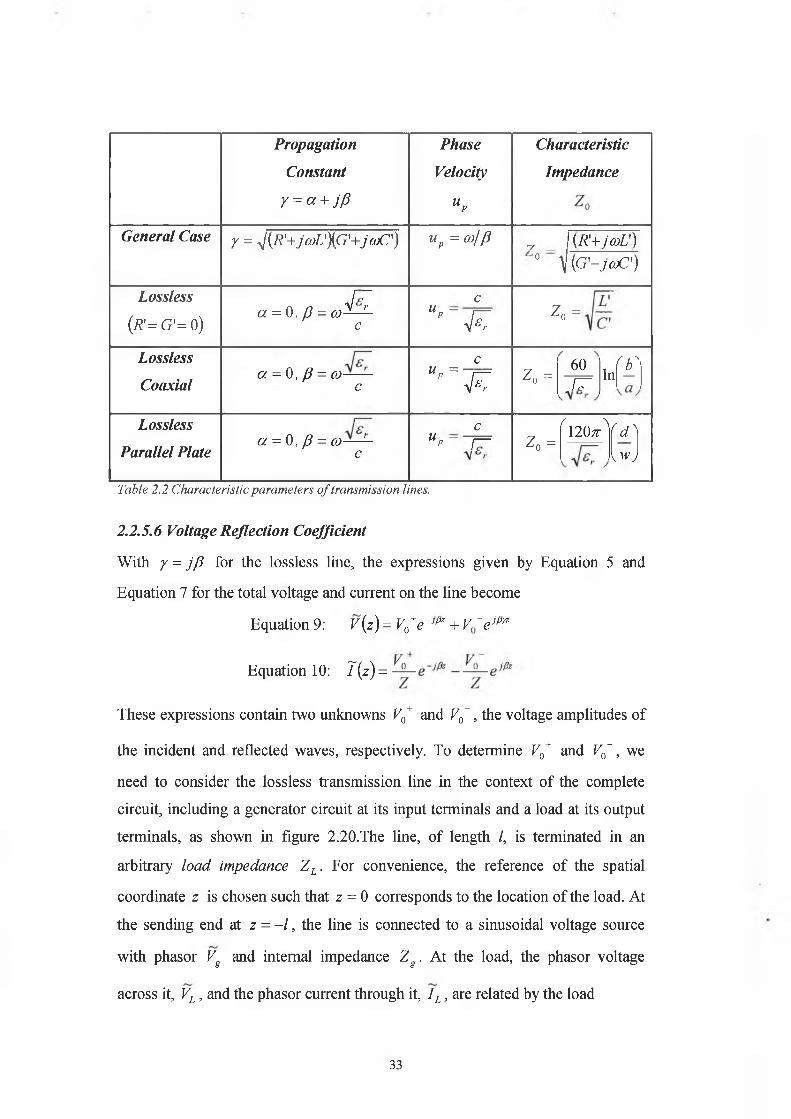
Propagation
Constant
Y = ct + j ¡3
Phase
Velocity
u p
Characteristic
Impedance
General Case y = y¡{R'+ja>L%G'+jcoC') up = cofp , I (*'+/<»£')0 Í(G '+jaC')
Lossless
(R'=G'= o)a = 0, P = co — -
c
cup ~ 1—
4 £ r
IIoN
Lossless
Coaxiala - 0 , p = co——
c
cuP = - r =
y l £ rZ o =
60 I,
r ~ lr( b '
l —
Lossless
Parallel Platea = 0, p = co '
c
cup ~ ~ j = Z 0 =
/ \
120^ r d"' Vw )
Table 2.2 Characteristic parameters o f transmission lines.
2.2.5.6 Voltage Reflection Coefficient
With y = JP for the lossless line, the expressions given by Equation 5 and
Equation 7 for the total voltage and current on the line become
Equation 9: V(z) = F0V J/fe + V~eJPrt
Equation 10: 7{z) =
These expressions contain two unknowns V0+ and V0~, the voltage amplitudes of
the incident and reflected waves, respectively. To determine V0+ and V0~, we
need to consider the lossless transmission line in the context of the complete
circuit, including a generator circuit at its input terminals and a load at its output
terminals, as shown in figure 2.20.The line, of length /, is terminated in an
arbitrary load impedance ZL. For convenience, the reference of the spatial
coordinate z is chosen such that z = 0 corresponds to the location of the load. At
the sending end at z = - / , the line is connected to a sinusoidal voltage source
with phasor Vg and internal impedance Zg . At the load, the phasor voltage
across it, VL, and the phasor current through it, 1L, are related by the load
33
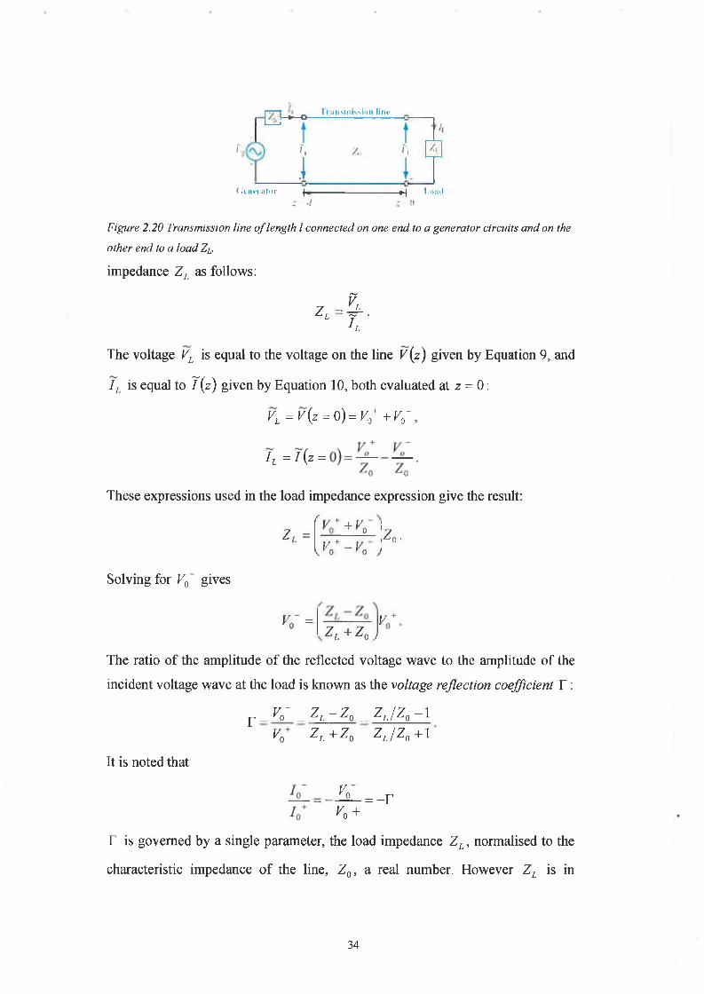
-*—o- T r jiiis in is s iim liru-
i( • i'll iTii tor h =p~\ I , D i l l]
Figure 2.20 Transmission line o f length I connected on one end to a generator circuits and on the
other end to a load Zi.
impedance ZL as follows:
ZLS .h
The voltage VL is equal to the voltage on the line V(z) given by Equation 9, and
I L is equal to 7 (z) given by Equation 10, both evaluated at z = 0:
VL = v(z = o ) = v ; + v ; ,
i l = i ( z =
These expressions used in the load impedance expression give the result:
2 , =f y + + y ^ ' 0
V * - VVr o ’ o yR e
solving for V0 gives
K~ = v +y rtZL + Z0 J
The ratio of the amplitude of the reflected voltage wave to the amplitude of the
incident voltage wave at the load is known as the voltage reflection coefficient Y :
F_V0- _ zL- z 0 __ ZL/Z 0 -1 v0 ZL + Z0 ZL/Z 0 +1
It is noted that
K
Vo += - r
r is governed by a single parameter, the load impedance ZL, normalised to the
characteristic impedance of the line, Z0, a real number. However ZL is in
34
general a complex quantity, as in the case of a series RL circuit, for example, for
which ZL = R + jcoL . Hence in general r may be complex also:
r = \r\eM
where |r| is the magnitude of r and 6r is its phase angle. Note that |r| < 1.
A load is said to be matched to the line if ZL = Z0 because then there will
be no reflection by the load (T = 0 and V0~ =0) . On the other hand, when the
load is an open circuit (Z L = oo), r = 1 and V0~ = V()+, and when it is a short
circuit (Z L =0) , T = -1 and V0~ = -V0+.
2.2.5.7 Standing Waves
Using the relation V0~ =FV0+ in Equation 9 and Equation 10 gives the
expressions
Equation 11: V(z) = V0+ (e~^2 + YejPyz)
Equation 12: 7 (z) = - 2 - i f Jik - Tejpp )Zq
which now contain only one, yet to be determined unknown, V0+. Before solving
for this unknown, it is important to examine the physical meaning represented by
these expressions. Firstly an expression for V(z)|, the magnitude of V(z), is
derived. Using r = |r|e^' in Equation 11 and applying the relation
V(z)| = [v(z)V * (z)], where V * (z) is the complex conjugate of V(z) gives:
F(z)| = {v0+ (e-Jflz + | r y V ,/& )][(f0+ )* (ejiiz + \T\e~jdr e~Jiiz
= F0+|[i + |r|2 +|r|(ey(2/fe+ ) + e-y(2 ))]^
= f-0+|[i + |r|2 + 2|r| cos(2 /3z + er ) f 2
where we have the identity
eJX +e~JX = 2cosx
for any real quantity x . By applying the same steps to Equation 12, a similar
expression can be derived for |7(z)|, the magnitude of the current 7(z).
35
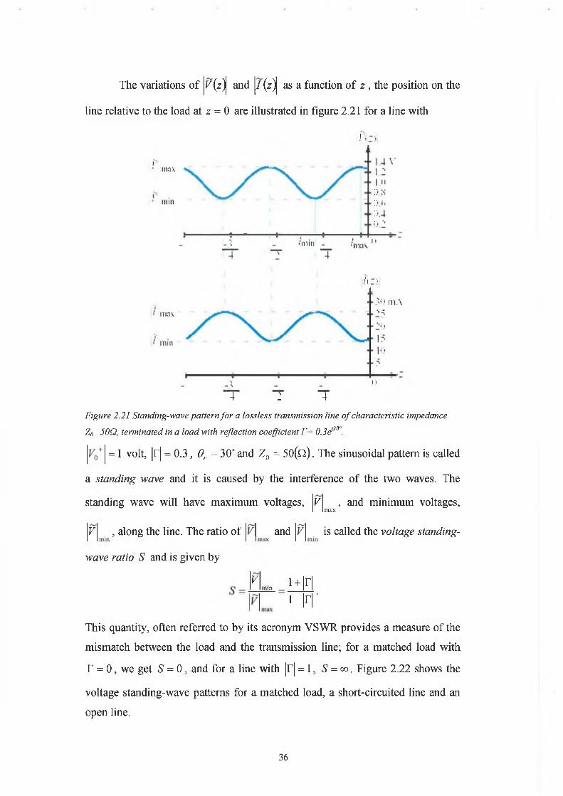
The variations of V(z)j and |/(z)j as a function of z , the position on the
line relative to the load at z = 0 are illustrated in figure 2.21 for a line with
! ■
!\ z •
4 : 4Figure 2.21 Standing-wave pattern fo r a lossless transmission line o f characteristic impedance
Z0=50Q, terminated in a load with reflection coefficient 1' 0.3é i0 .
= 1 volt, |r| = 0.3, 6r = 30° and Z0 = 50(q) . The sinusoidal pattern is called
a standing wave and it is caused by the interference of the two waves. The
standing wave will have maximum voltages, V
V , along the line. The ratio of and
, and minimum voltages,max
is called the voltage standing-
wave ratio S and is given by
V - l + lr l 1—lr |
This quantity, often referred to by its acronym VSWR provides a measure of the
mismatch between the load and the transmission line; for a matched load with
T = 0 , we get S = 0 , and for a line with |F| = 1, S = oo. Figure 2.22 shows the
voltage standing-wave patterns for a matched load, a short-circuited line and an
open line.
36
Nkiklk'l lino
4 2 4Figure 2.22 a)ZL=Z0, matched line.
4 : 4
Figure 2.22 b) ZL=0, short circuit.
4 . 2 4
Figure 2.22 c) Z]j= qo, open circuit.
2.2.5.8 Input Impedance o f the lossless Line
The standing-wave patterns indicate that for a mismatched line the voltage and
current magnitudes are oscillatory with position on the line and in phase
opposition with each other. Hence, the voltage to current ratio, called the input
impedance Zm, must also vary with position. Using Equation 11 and Equation
12, Zin is given by
+
1
e - j P * + r e J , i z
7 — 7
’ i + r v ' 2 / ? z
7 ( z ) v 0 +
1
1
h1 >
1 __
__
__
__
__
__
__
__
__
__
__
__
__
__
__
__
__
__
__
__
__
__
_
i - r ^ 2 / ? z
Note that Zin (z) is the ratio of the total voltage (incident-wave and reflected-
wave voltages) to the total current at any point z on the line, in contrast with the
characteristic impedance of the line Z0, which relates the voltage and current of
each of the two waves individually (z „ = i/o V v = - ( /o"Ao").
Of particular interest in many transmission-line problems is the input
impedance at the input of the line at z = - / , which is given by
37
Equation 13 : Zin ( - /) = Z0 em + Y e m = Zr \+Ye~iiptl - Y eem _ Ye-m
Using T = ZL/Z 0 -1 /Z i /Z 0 +1 and the relations
elP = cos p i + j sin p i ,e~jP = cos y61 - j sin pi
Equation 13 can be written in terms of ZL as
-J20I
z,„(-0 =z.ZL cos p i + jZ 0 sin pi
= Zr ZL + jZ Q tan pi Z0 + jZ L tan piZ0 cos pi + jZ L sin pi
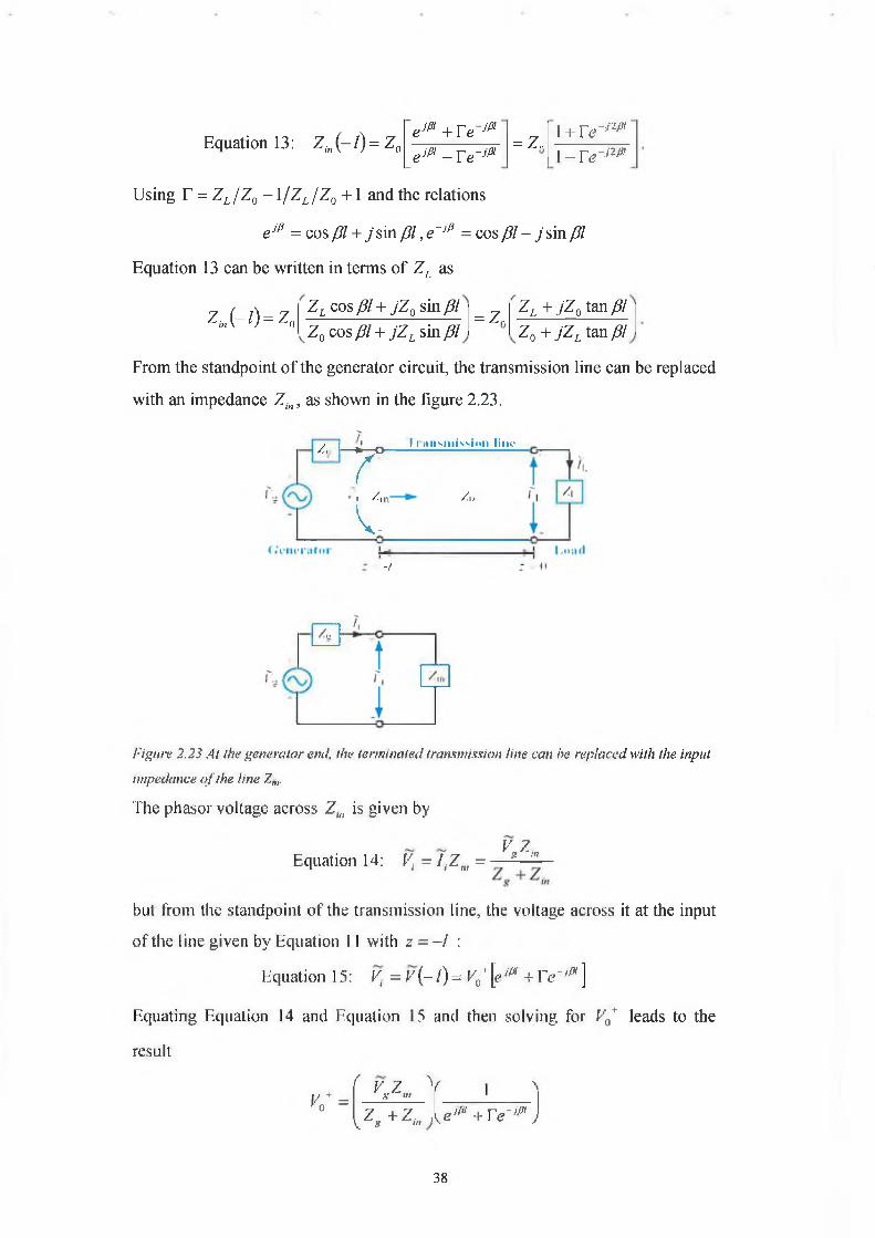
From the standpoint of the generator circuit, the transmission line can be replaced
with an impedance Z,„, as shown in the figure 2.23.
/, I—►—o- I I ,I I IM l l i s s i l . l l l i n o
f[l /,
V/,>
-I
l-'igure 2.23 Al the generator end, the terminated transmission tine can he replaced with the input
impedance o f I he line Z,„.
The phasor voltage across Zin is given by
Equation 14: Vi = I tZm = —V Zg m
but from the standpoint of the transmission line, the voltage across it at the input
of the line given by Equation 11 with z = -I :
Equation 15: V, = V (- l)= K0+[e> + n ? '>/s]
Equating Equation 14 and Equation 15 and then solving for V0+ leads to the
result
V + =yo( V Z. )g in
{ 1 ÌZ + z\ 8 In U ;/J,+ r e ' ipi)
38
This completes the solution of the transmission-line wave equations, given by
Equation 3 and Equation 4 for the special case of a lossless transmission line.
Finally, some important relationships are noted. A network analyser is a
radio-frequency instrument capable of measuring the impedance of any load
connected to its input terminal. When used to measure Z ™, the input impedance
of a lossless line terminated in a short circuit, and again Z°°n , the input impedance
of the line when terminated in an open circuit, the combination of the two
measurements can be used to determine the characteristic impedance of the line
Z0 and its phase constant f t . It can be shown that
A matched lossless transmission line with ZL = Z 0, has input impedance
Zm = Z0 for all locations on the line, r = 0 and all the incident power is
delivered to the load regardless of the line length /.
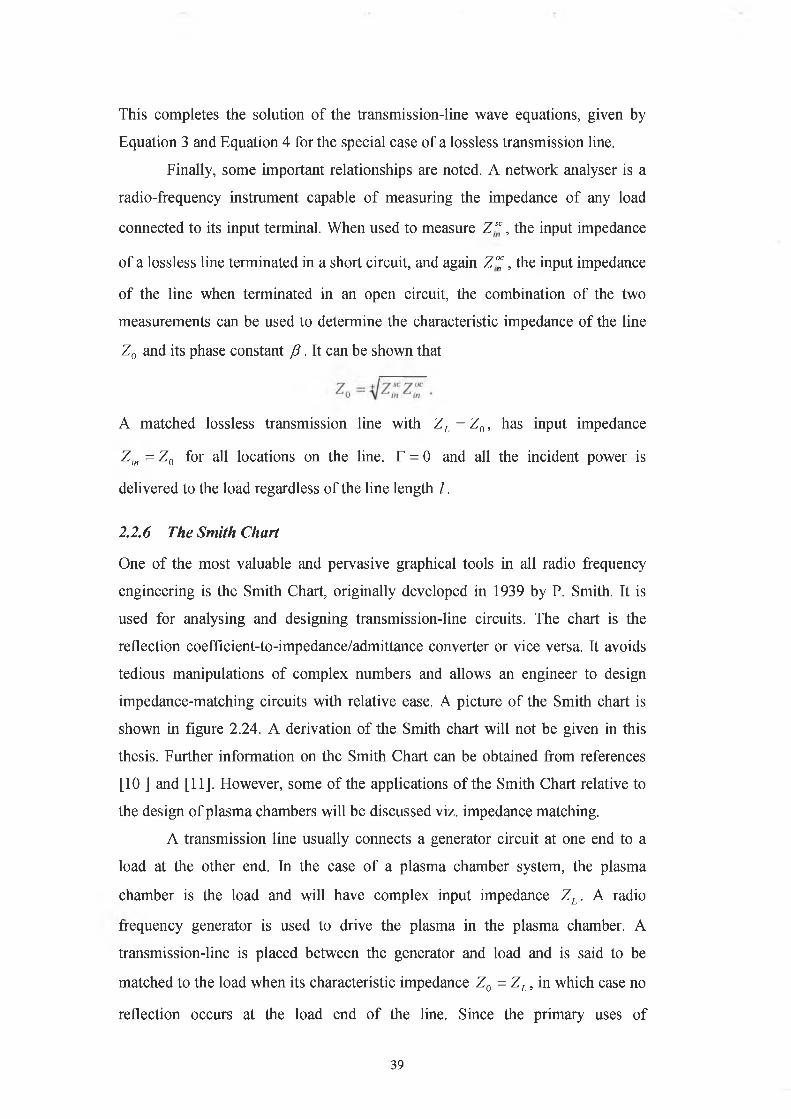
2.2.6 The Smith Chart
One of the most valuable and pervasive graphical tools in all radio frequency
engineering is the Smith Chart, originally developed in 1939 by P. Smith. It is
used for analysing and designing transmission-line circuits. The chart is the
reflection coefficient-to-impedance/admittance converter or vice versa. It avoids
tedious manipulations of complex numbers and allows an engineer to design
impedance-matching circuits with relative ease. A picture of the Smith chart is
shown in figure 2.24. A derivation of the Smith chart will not be given in this
thesis. Further information on the Smith Chart can be obtained from references
[10 ] and [11]. However, some of the applications of the Smith Chart relative to
the design of plasma chambers will be discussed viz. impedance matching.
A transmission line usually connects a generator circuit at one end to a
load at the other end. In the case of a plasma chamber system, the plasma
chamber is the load and will have complex input impedance ZL. A radio
frequency generator is used to drive the plasma in the plasma chamber. A
transmission-line is placed between the generator and load and is said to be
matched to the load when its characteristic impedance Z0 = Z L, in which case no
reflection occurs at the load end of the line. Since the primary uses of
39
transmission lines are to transfer power, a matched load ensures that the power
delivered to the load is a maximum.
Figure 2.24 The Smith Chart
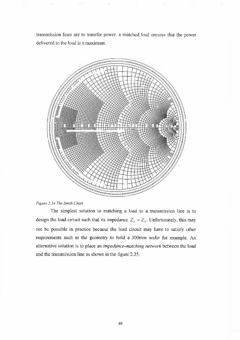
The simplest solution to matching a load to a transmission line is to
design the load circuit such that its impedance ZL - Z0. Unfortunately, this may
not be possible in practice because the load circuit may have to satisfy other
requirements such as the geometry to hold a 300mm wafer for example. An
alternative solution is to place an impedance-matching network between the load
and the transmission line as shown in the figure 2.25.
40
Figure 2.25 The function o f a matching network is to transform the load impedance ZL such that
the input impedance Zin looking into the network is equal to Z0 o f the transmission line.
The purpose of the matching network is to eliminate reflections at the
juncture MM’ between the transmission line and the network. This is achieved by
designing the matching network to exhibit an impedance equal to Z0 at MM’
when looking into the network from the transmission line side. If the network is
lossless, then all the power going into it will end up in the load. Matching
networks may consist of lumped elements and in order to avoid ohmic losses only
capacitors and inductors are used.
The matching network is intended to match a load impedance
ZL = Rl + jX L to a lossless transmission line with characteristic impedance Z0.
This means that the network has to transform the real part of the load impedance
from R, at the load to Z0 at MM’ in figure 2.25 and to transform the reactive
part from X L at the load to zero at MM’. The matching network has to have at
least two degrees of freedom to achieve these two transformations; i.e. at least
two adjustable parameters. There are many different types of matching network
that can be used for plasma chambers. The components used in the matching
network will depend on the complex impedance of the plasma chamber. When
designing matching networks four main criteria should be considered:
• Simplicity
The simplest design is usually highly preferable because simpler
matching networks have fewer elements, require less work to
manufacture, are cheaper, are less lossy and are more reliable
compared to a more complicated and involved design.
41
• Bandwidth
Any matching network can provide zero reflection at a single
frequency; however, if impedance matching over a frequency band is
required then more complex designs need to be used. Thus, there is a
trade-off between design simplicity and matching bandwidth and
eventually the network price.
• Feasibility of manufacturing
The plasma chamber system parameters have to be considered when
designing a matching network. Clear specifications for the plasma
chamber’s impedance range, breakdown voltage and breakdown
current must be determined so that the matching network will be able
to function within the system and not become a limiting factor to the
system.
• Ease of tunability
Variable loads such as plasma chambers require variable tuning. Thus,
the matching network design and implementation should take account
of this by, for example, employing feedback systems.
2.2.7 Insertion Loss
The insertion loss is the attenuation resulting from inserting a circuit between the
source (e.g. a radio frequency generator) and the load (e.g. a plasma chamber).
The attenuation is expressed in decibels (dB). The unit for power P is watts (W).
When considering insertion loss the quantity of interest is the ratio of two power
levels, Pi and P2, such as the incident and reflected powers on a transmission
line. The ratio P1/P2 may often vary over several orders of magnitude. The dB
scale is logarithmic, thereby providing a convenient representation of the power
ratio, particularly when numerical values of P1/P2 are plotted against some
variable of interest. If
P 2
then
GdB = lOlogG = 10 logr P ^
PK1 2 J(dB).
42
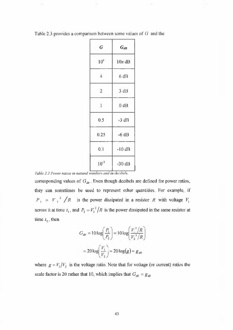
Table 2.3 provides a comparison between some values of G and the
G GdB
10* lOx dB
4 6dB
2 3 dB
1 0 dB
0.5 -3 dB
0.25 -6 dB
0.1 -10 dB
10'3 -30 dB
Table 2.3 Power ratios in natural numbers anil in decibels.
corresponding values of GdB . Even though decibels are defined for power ratios,
they can sometimes be used to represent other quantities. For example, if
P i = F V 2 A is the power dissipated in a resistor R with voltage Vl
across it at time t1, and P2 - V 2 ¡R is the power dissipated in the same resistor at
time t2, then
r v ' /RGjb = 10 log = 10 log
20 log = 201og(g)=gde
where g = VjV 2 is the voltage ratio. Note that for voltage (or current) ratios the
scale factor is 20 rather that 10, which implies that GdB = g dB
43
2.3 Plasma Theory
2.3.1 An overview o f Plasma
A plasma is a collection of free, charged particles moving in random directions
that are, on the average, electrically neutral. The semiconductor industry
generally uses weakly ionised plasma discharges which have the following
properties:
• They are driven electrically.
• Charged particle collisions with neutral gas molecules are important.
• There are boundaries at which surface losses are important.
• Ionisation of neutrals sustains the plasma in the steady state.
• The electrons are not in thermal equilibrium with the ions.
A simple discharge is shown schematically in figure 2.26. It consists of a
Figure 2.26 Schematic o f a simple discharge
voltage source that drives current through a low-pressure gas between two
parallel conducting electrodes. The gas “breaks down” to form plasma that is
usually weakly ionised, i.e. the plasma density is only a small fraction of the
neutral gas density. Plasmas are often called a fourth state of matter. A solid
substance in thermal equilibrium generally passes into a liquid state as the
temperature is increased at a fixed pressure. The liquid passes into a gas as the
temperature is further increased. At sufficiently high temperature, the molecules
in the gas decompose to form a gas of atoms that move freely in random
directions, except for infrequent collisions between atoms. It the temperature is
further increased, then the atoms decompose into freely moving charged particles
(electrons and positive ions), and the substance enters the plasma state. This state
is characterised by a common charged particle density ne~ n,~ n particles/m3 and,
in equilibrium, a temperature Te = T; = T. The temperatures required to form
plasmas from pure substances in thermal equilibrium range from roughly 4000 K
zElectrode
+Gas
44
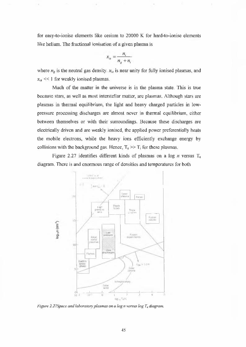
for easy-to-ionise elements like cesium to 20000 K for hard-to-ionise elements
like helium. The fractional ionisation of a given plasma is
where ng is the neutral gas density. xvz is near unity for fully ionised plasmas, and
Xiz « 1 for weakly ionised plasmas.
Much of the matter in the universe is in the plasma state. This is true
because stars, as well as most interstellar matter, are plasmas. Although stars are
plasmas in thermal equilibrium, the light and heavy charged particles in low-
pressure processing discharges are almost never in thermal equilibrium, either
between themselves or with their surroundings. Because these discharges are
electrically driven and are weakly ionised, the applied power preferentially heats
the mobile electrons, while the heavy ions efficiently exchange energy by
collisions with the background gas. Hence, Te » T; for these plasmas.
Figure 2.27 identifies different kinds of plasmas on a log n versus Te
diagram. There is and enormous range of densities and temperatures for both
V/ Laser ______
plasma Focus
Highpressure
arcs
Shocktubes
Thetapinches
OL______i______ I-----------------¿CJ---- 1----L---------LIO' 2 IO“1 0 1 2 3 4logio Te(V)
Figure 2.27Space and laboratory plasmas on a log n versus log Te diagram.
45
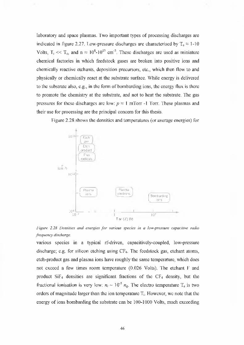
laboratory and space plasmas. Two important types of processing discharges are
indicated in figure 2.27. Low-pressure discharges are characterised by Te ~ 1-10
Volts, Ti « Te, and n ~ 108-1013 cm'3. These discharges are used as miniature
chemical factories in which feedstock gases are broken into positive ions and
chemically reactive etchants, deposition precursors, etc., which then flow to and
physically or chemically react at the substrate surface. While energy is delivered
to the substrate also, e.g., in the form of bombarding ions, the energy flux is there
to promote the chemistry at the substrate, and not to heat the substrate. The gas
pressures for these discharges are low: p ~ 1 mTorr -1 Torr. These plasmas and
their use for processing are the principal concern for this thesis.
Figure 2.28 shows the densities and temperatures (or average energies) for
n(cm -3)
1012
108
Etch
gas
Etch
product j
-( Free
radicals
£Plasma
ions
Plasma
electronsBom barding
ions
10-2 10?
T o r (£ ) (V)
Figure 2.28 Densities and energies fo r various species in a low-pressure capacitive radio
frequency discharge.
various species in a typical rf-driven, capacitively-coupled, low-pressure
discharge; e.g. for silicon etching using CF4. The feedstock gas, etchant atoms,
etch-product gas and plasma ions have roughly the same temperature, which does
not exceed a few times room temperature (0.026 Volts). The etchant F and
product SiF4 densities are significant fractions of the C F 4 density, but the
fractional ionisation is very low: n, ~ 10'5 ng. The electro temperature Te is two
orders of magnitude larger than the ion temperature T;. However, we note that the
energy of ions bombarding the substrate can be 100-1000 Volts, much exceeding
46
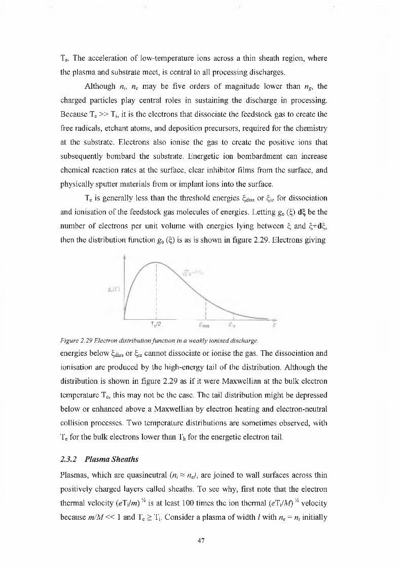
Te. The acceleration of low-temperature ions across a thin sheath region, where
the plasma and substrate meet, is central to all processing discharges.
Although n„ ne may be five orders of magnitude lower than ng, the
charged particles play central roles in sustaining the discharge in processing.
Because Te » T,, it is the electrons that dissociate the feedstock gas to create the
free radicals, etchant atoms, and deposition precursors, required for the chemistry
at the substrate. Electrons also ionise the gas to create the positive ions that
subsequently bombard the substrate. Energetic ion bombardment can increase
chemical reaction rates at the surface, clear inhibitor films from the surface, and
physically sputter materials from or implant ions into the surface.
Te is generally less than the threshold energies ^iss or lz for dissociation
and ionisation of the feedstock gas molecules of energies. Letting ge (£) di; be the
number of electrons per unit volume with energies lying between h, and ^+dq,
then the distribution function ge (Q is as is shown in figure 2.29. Electrons giving
Figure 2.29 Electron distribution function in a weakly ionised discharge.
energies below Çdiss or 1Z cannot dissociate or ionise the gas. The dissociation and
ionisation are produced by the high-energy tail of the distribution. Although the
distribution is shown in figure 2.29 as if it were Maxwellian at the bulk electron
temperature Te, this may not be the case. The tail distribution might be depressed
below or enhanced above a Maxwellian by electron heating and electron-neutral
collision processes. Two temperature distributions are sometimes observed, with
Te for the bulk electrons lower than Th for the energetic electron tail.
2.3.2 Plasma Sheaths
Plasmas, which are quasineutral (n, ~ ne), are joined to wall surfaces across thin
positively charged layers called sheaths. To see why, first note that the electron
thermal velocity (eTJm) % is at least 100 times the ion thermal {eTJM)Vl velocity
because m/M « 1 and Te > T;. Consider a plasma of width I with ne = n, initially
47
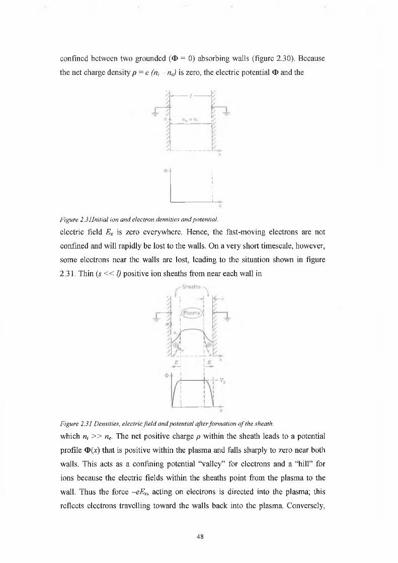
confined between two grounded (® = 0) absorbing walls (figure 2.30). Because
the net charge density p = e (rii - ne) is zero, the electric potential <D and the
‘A*----- 1/
<t>
Figure 2.3 ¡Initial ion and electron densities and potential.
electric field Ex is zero everywhere. Hence, the fast-moving electrons are not
confined and will rapidly be lost to the walls. On a very short timescale, however,
some electrons near the walls are lost, leading to the situation shown in figure
2.31. Thin (s « I) positive ion sheaths from near each wall in
Figure 2.31 Densities, electric fie ld and potential after formation o f the sheath.
which rii » ne. The net positive charge p within the sheath leads to a potential
profile <D(x) that is positive within the plasma and falls sharply to zero near both
walls. This acts as a confining potential “valley” for electrons and a “hill” for
ions because the electric fields within the sheaths point from the plasma to the
wall. Thus the force -e E x, acting on electrons is directed into the plasma; this
reflects electrons travelling toward the walls back into the plasma. Conversely,
i////
48
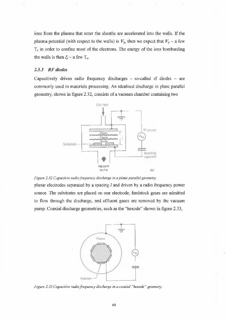
ions from the plasma that enter the sheaths are accelerated into the walls. If the
plasma potential (with respect to the walls) is Vp, then we expect that Vp ~ a few
Te in order to confine most of the electrons. The energy of the ions bombarding
the walls is then £ ~ a few Te.
2.3.3 RF diodes
Capacitively driven radio frequency discharges - so-called rf diodes - are
commonly used in materials processing. An idealised discharge in plane parallel
geometry, shown in figure 2.32, consists of a vacuum chamber containing two
Figure 2.32 Capacitive radio frequency discharge in a plane parallel geometry.
planar electrodes separated by a spacing I and driven by a radio frequency power
source. The substrates are placed on one electrode, feedstock gases are admitted
to flow through the discharge, and effluent gases are removed by the vacuum
pump. Coaxial discharge geometries, such as the “hexode” shown in figure 2.33,
Gas feed
Substrate —
Vacuumpump (a )
X
Substrate JFigure 2.33 Capacitive radio frequency discharge in a coaxial "hexode" geometry.
49
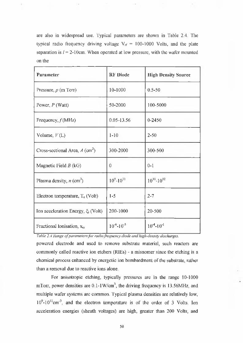
are also in widespread use. Typical parameters are shown in Table 2.4. The
typical radio frequency driving voltage Vrf = 100-1000 Volts, and the plate
separation is / = 2-10cm. When operated at low pressure, with the wafer mounted
on the
Parameter RF Diode High Density Source
Pressure,/) (m Torr) 10-1000 0.5-50
Power, P (Watt) 50-2000 100-5000
Frequency,/ (MHz) 0.05-13.56 0-2450
Volume, V (L) 1-10 2-50
Cross-sectional Area, A (cm2) 300-2000 300-500
Magnetic Field B (kG) 0 0-1
Plasma density, n (cm3) 109-10n 1010-1012
Electron temperature, Te (Volt) 1-5 2-7
Ion acceleration Energy, ^ (Volt) 200-1000 20-500
Fractional Ionisation, xiz 10'6-10'3 lO'MO'1
Table 2.4 Range ofparameters fo r radio frequency diode and high-density discharges.
powered electrode and used to remove substrate material, such reactors are
commonly called reactive ion etchers (RIEs) - a misnomer since the etching is a
chemical process enhanced by energetic ion bombardment of the substrate, rather
than a removal due to reactive ions alone.
For anisotropic etching, typically pressures are in the range 10-1000
mTorr, power densities are 0.1-lW/cm3, the driving frequency is 13.56MHz, and
multiple wafer systems are common. Typical plasma densities are relatively low,
109-10ucm'3, and the electron temperature is of the order of 3 Volts. Ion
acceleration energies (sheath voltages) are high, greater than 200 Volts, and
50
fractional ionisation is low. The degree of dissociation of the molecules into
reactive species is seldom measured but can range widely from less than 0.1% to
nearly 100% depending on gas composition and plasma conditions. For
deposition and isotropic etch applications, pressures tend to be higher, ion
bombarding energies are lower, and frequencies can be lower than the commonly
used standard of 13.56MHz.
The operation of capacitively driven discharges is reasonably well
understood. As shown in figure 2.34, for a symmetrically driven discharge, the
Sheath a Sheath b
Figure 2.34 The physical model o f a radio frequency diode.
mobile plasma electrons, responding to the instantaneous electric fields produced
by the radio frequency driving voltage, oscillate back and forth within the
positive space charge cloud of the ions. The massive ions respond only to the
time-averaged electric fields. Oscillation of the electron cloud creates sheath
regions near each electrode that contain net positive charge when averaged over
an oscillation period; i.e., the positive charge exceeds the negative charge in the
system, with the excess appearing in the sheaths. This excess produces a strong
time-averaged electric field within each sheath directed from the plasma to the
electrode. Ions flowing out of the bulk plasma near the centre of the discharge
51
can be accelerated by the sheath fields to high energies as they flow to the
substrate, leading to energetic ion enhanced processes. Typical ion bombardment
energies £ can be as high as Vrf/2 for symmetric systems and as high as V,f at the
powered electrode for asymmetric systems.
The positive ions continuously bombard the electrode over a radio
frequency cycle. In contrast, electrons are lost to the electrode only when the
oscillating cloud closely approaches the electrode. During that time, the
instantaneous sheath potential collapses near zero allowing sufficient electrons to
escape to balance the ion charge delivered to the electrode. Except for such brief
moments, the instantaneous potential of the discharge must always be positive
with respect to any large electrode and wall surface; otherwise the mobile
electrons would quickly leak out. Electron confinement is ensured by the
presence of positive space charge sheaths near all surfaces.
A crucial limiting feature of radio frequency diodes is that the ion
bombarding flux T; = nus and bombarding energy £ cannot be varied
independently. The situation is analogous to the lack of independent voltage and
current control in diode vacuum tubes or semiconductor pn junctions. For a
reasonable (but relatively low) ion flux, as well as a reasonable dissociation of the
feedstock gas, sheath voltages at the driven electrode are high. For wafers placed
on the driven electrode, this can result in undesirable damage, or loss of line
width control. Furthermore, the combination of low flux and high ion energy
leads to a relatively narrow process window for many applications. The low
process rates resulting from the limited ion flux in radio frequency diodes often
mandates multiwafer or batch processing, with consequent loss of wafer to wafer
reproducibility. Higher ion and neutral fluxes are generally required for single
wafer processing in a clustered tool environment, in which a single wafer is
moved by a robot through a series of process chambers. Clustered tools are used
to control interface quality and are said to have the potential for significant cost
savings in fabricating integrated circuits.
Although the need for low pressures, high fluxes, and controllable ion
energies has motivated high-density source development, there are many issues
that need to be resolved. A critical issue is achieving the required process
uniformity over 200mm to 300mm wafer diameters. In contrast to the nearly one
52
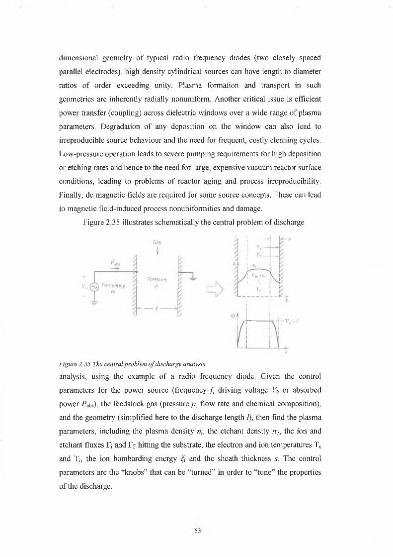
dimensional geometry of typical radio frequency diodes (two closely spaced
parallel electrodes), high density cylindrical sources can have length to diameter
ratios of order exceeding unity. Plasma formation and transport in such
geometries are inherently radially nonuniform. Another critical issue is efficient
power transfer (coupling) across dielectric windows over a wide range of plasma
parameters. Degradation of any deposition on the window can also lead to
irreproducible source behaviour and the need for frequent, costly cleaning cycles.
Low-pressure operation leads to severe pumping requirements for high deposition
or etching rates and hence to the need for large, expensive vacuum reactor surface
conditions, leading to problems of reactor aging and process irreproducibility.
Finally, dc magnetic fields are required for some source concepts. These can lead
to magnetic field-induced process nonuniformities and damage.
Figure 2.35 illustrates schematically the central problem of discharge
Figure 2.35 The central problem o f discharge analysis.
analysis, using the example of a radio frequency diode. Given the control
parameters for the power source (frequency / , driving voltage Fj or absorbed
power Pabs), the feedstock gas (pressure p, flow rate and chemical composition),
and the geometry (simplified here to the discharge length /), then find the plasma
parameters, including the plasma density «„ the etchant density n?, the ion and
etchant fluxes Ti and Tf hitting the substrate, the electron and ion temperatures Te
and Ti, the ion bombarding energy £ and the sheath thickness s. The control
parameters are the “knobs” that can be “turned” in order to “tune” the properties
of the discharge.
The tuning range of a given discharge is generally limited. Sometimes one
type of discharge will not do the job no matter how it is tuned, so another type
must be selected. As a result there is a big variety of discharges used for
processing. Some are driven by radio frequency, some by direct current and some
by microwave discharges. Some use magnetic fields to increase the plasma
confinement or the efficiency of power absorption. A capacitively coupled
plasma discharge has been used in this thesis. It is a relatively simple plasma
chamber. If this chamber can be modelled, as is the ultimate goal of this work,
then the modelling techniques can be applied to more complicated systems. A
theoretical model of a capacitively coupled discharge is given in the next section.
2.3.4 Theoretical Model o f a Capacitively Coupled Plasma Discharge
A complete description of a plasma discharge requires a choice of heating
mechanisms and geometric configuration that sustains those mechanisms. One of
the most widely used types of low pressure discharges is sustained by radio
frequency currents and voltage, introduced through a capacitive sheath. The
currents in the main body of the plasma lead to ohmic heating, while the voltage
across the sheath leads to stochastic sheath heating. The complete self-consistent
model of such a discharge is quite complicated, even in the simplest plane-
parallel geometry. This leads to various simplifying assumptions in order to
obtain analytic solutions in which the scalings of plasma parameters with control
parameters are explicit.
A uniform, symmetric model for a capacitive parallel-plate radio
frequency discharge was developed by V.A. Godyak et al [4], A brief description
of its derivation is given. The model is qualitively correct but, because
simplifying assumptions are made, cannot be used to predict the quantitive
behaviour of “real” discharges. Most discharges are asymmetric because more
electrode surfaces are naturally grounded rather than driven. This leads to a DC
bias voltage on the driven electrode with respect to ground. A brief description of
the asymmetric model is also given.
Figure 2.36 shows the basic homogenous model. A sinusoidal current
Ir[(t), having complex representation Trf = Re / rf e mt, flows across discharge plates
a and b. 7rf is taken to be a real number I\. The plates are separated by a distance /
and each has a cross sectional area A. A gas having neutral density ng is present
54
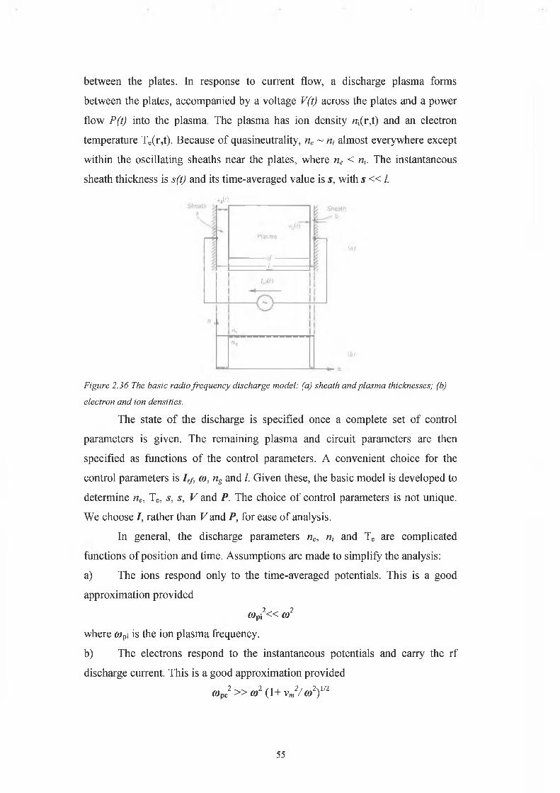
between the plates. In response to current flow, a discharge plasma forms
between the plates, accompanied by a voltage V(t) across the plates and a power
flow P(t) into the plasma. The plasma has ion density «¡(r,t) and an electron
temperature Te(r,t). Because of quasineutrality, ne ~ n, almost everywhere except
within the oscillating sheaths near the plates, where ne < n,. The instantaneous
sheath thickness is s(t) and its time-averaged value is s, with s « I
sa(t)
Figure 2.36 The basic radio frequency discharge model: (a) sheath and plasma thicknesses; (b)
electron and ion densities.
The state of the discharge is specified once a complete set of control
parameters is given. The remaining plasma and circuit parameters are then
specified as functions of the control parameters. A convenient choice for the
control parameters is Irf, (o, ng and I. Given these, the basic model is developed to
determine ne, Te, s, s, V and P. The choice of control parameters is not unique.
We choose /, rather than V and P, for ease of analysis.
In general, the discharge parameters ne, n, and Te are complicated
functions of position and time. Assumptions are made to simplify the analysis:
a) The ions respond only to the time-averaged potentials. This is a good
approximation provided
Wpi2« a)2
where e>Pi is the ion plasma frequency.
b) The electrons respond to the instantaneous potentials and carry the rf
discharge current. This is a good approximation provided2 - 2 /i i 2 / 2\l/2
Ope » 0 ) (1 + V m / Q ) )
55
c) The electron density is zero within the sheath regions. This is a good
approximation provided ^De « s where A,oe is the electron Debye length. This
holds if Te« V, where V is the DC voltage across the sheath.
d) There is no transverse variation (along the plates). This is a good
approximation provided l«^ A . Since the divergence of Maxwell’s equation
curl.(H) = J + e<s5EI5t is zero, we see that at any instant of time, the sum of the
conduction current J and the displacement current s^dEldt within the discharge is
then independent of x.
2.3.4.1 Plasma Admittance
The admittance of a bulk plasma slab of thickness d and cross-sectional area A is
Fp =j(o e^Ald, where
G>{co-jv ra)X /
is the plasma dielectric constant. Within the uniform ion density approximation
d = l-2s = const
independent of time. It is then found that
Yf =jc»C0 + — 7 - ■
j(oLp + R p
where C0 = s0 AJd is the vacuum capacitance, Lp = a)ve2Co~l is the plasma
inductance, and Rp = vm Lp is the plasma resistance. This form of Yp represents the
series combination of Lp and Rp in parallel with Co. By assumption b), the
displacement current that flows through Co is much smaller that the conduction
current that flows through Lp and Rp. The sinusoidal current
/,/t) = Re V " '
that flows through the plasma bulk produces a voltage across the plasma
Vp(t) = Re Vp€ mt
where Vp = Irf / Fp is the complex voltage amplitude. We see that the plasma
voltage is linear in the applied current and that there is no harmonic generation or
DC component of Vp.
2.3.4.2 Sheath Admittance
In contrast to the plasma, the current that flows through the two sheaths is almost
entirely displacement current; i.e. it is due to a time-varying electric field. This is
56
true because the conduction current in a discharge is carried mainly by electrons,
and the electron density is approximately zero within the time-varying sheath. We
will see that the conduction current carried by the steady flow of ions across the
sheath to the plates is much smaller than the displacement current,
a) Displacement Current The electric field E = xE within sheath a (see figure
2.36) is given by Poisson’s equation
dE en— = — , * < s „ ( i )
U X
which on integration yields
E{x,t) = — ( x - s a{t))£ 0
The boundary condition is E ~ 0 at x — sa because E is continuous across the
plasma-sheath interface (no surface charge) and the electric field is small in the
plasma. The displacement current flowing through sheath a into the plasma is
7 / \ A S E
/.<*>=
Substituting the previous two equations we get
&~8 t
We see that the sheath boundary sa oscillates linearly with the applied current.
Setting Iap(t) = Irf(t), where 7rf = /icos cot, we integrate the above equation to get
sa = s - s 0 sin cot
where
I
IaP (0 = ~enA~
encoA
is the sinusoidal oscillation amplitude about the DC value s. The voltage across
the sheath is given bys 2
V„p(t) = jE d x : en s„e0 2
From this expression the sheath voltage is a nonlinear function of sa and therefore
of the applied current. Substituting the equation for sa into the above equation we
57
get
enF .. =
ap 2 s
f i js 2 + —sn - 2 ssnsma>t— sn cos 2cot
o V 2 2
We see the nonlinearity leads to second-harmonic voltage generation and a
constant average value.
Similarly for the sheath b we obtain
h P (0 = ~enA^ rot
and the voltage across this sheath is
v en s »2
bp 0 2
By continuity of current, /bp = -/ap, therefore
Integrating, we obtain
sa + s b = 2 s ,
a constant so that d = I - 2s = const, as previously stated. For sheath b,
sb = s + s0 sin cot
with the nonlinear voltage response,
enVoP = -
f ] i \s 2 + — s0 - 2 s s 0smcot— s02cos2iy/
■o v ^ ^ y
Although Fap and FbP are nonlinear, the combined voltage Fab = Fap - Fbp
across both sheaths is
ens,
Substituting for Sb and sa we find
2 enssnVab = ~ 0 sin cot
'0
which is a linear voltage response. We obtain the surprising result that although
each sheath is nonlinear, the combined effect of both sheaths is linear. This is true
only for the simplified model assumptions of a symmetric, homogeneous
(constant ion density) discharge. The total voltage Frf across the discharge is the
58
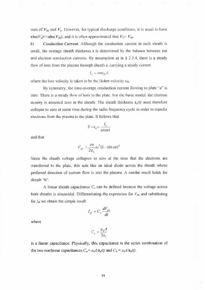
sum of and V9. However, for typical discharge conditions, it is usual to have
abs(i/p)« a h s(F ab), and it is often approximated that Vrf= Vab.
b) Conduction Current. Although the conduction current in each sheath is
small, the average sheath thickness s is determined by the balance between ion
and electron conduction currents. By assumption a) in § 2.3.4, there is a steady
flow of ions from the plasma through sheath a, carrying a steady current
/, = enunA
where the loss velocity is taken to be the Bohm velocity i/b .
By symmetry, the time-average conduction current flowing to plate “a” is
zero. There is a steady flow of ions to the plate. For the basic model, the electron
density is assumed zero in the sheath. The sheath thickness sa(t) must therefore
collapse to zero at some time during the radio frequency cycle in order to transfer
electrons from the plasma to the plate. It follows that
s =sQ= —encoA
and that
Vpa = ^ - s o 2( l - s i n < a f ) 2z s 0
Since the sheath voltage collapses to zero at the time that the electrons are
transferred to the plate, this acts like an ideal diode across the sheath whose
preferred direction of current How is into the plasma. A similar result holds for
sheath "b”.
A linear sheath capacitance Cs can be defined because the voltage across
both sheaths is sinusoidal. Differentiating the expression for V& and substituting
for /rp we obtain the simple result
where
r S ° A
s 2 s0
is a linear capacitance. Physically, this capacitance is the series combination of
the two nonlinear capacitances Ca= eoA/s/t) and Cb = eoA/s\,(t).
59
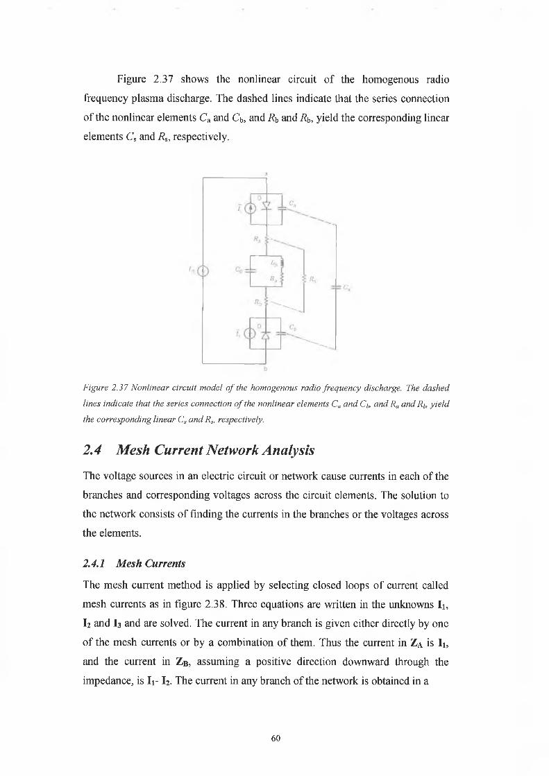
Figure 2.37 shows the nonlinear circuit of the homogenous radio
frequency plasma discharge. The dashed lines indicate that the series connection
of the nonlinear elements Ca and Cb, and R\, and Rb, yield the corresponding linear
elements Cs and Rs, respectively.
a
Figure 2.37 Nonlinear circuit model o f the homogenous radio frequency discharge. The dashed
lines indicate that the series connection o f the nonlinear elements Ca and C*, and R„ and Rt, yield
the corresponding linear Cs andRs, respectively.
2.4 Mesh Current Network Analysis
The voltage sources in an electric circuit or network cause currents in each of the
branches and corresponding voltages across the circuit elements. The solution to
the network consists of finding the currents in the branches or the voltages across
the elements.
2.4.1 Mesh Currents
The mesh current method is applied by selecting closed loops of current called
mesh currents as in figure 2.38. Three equations are written in the unknowns Ii,
h and I3 and are solved. The current in any branch is given either directly by one
of the mesh currents or by a combination of them. Thus the current in Z \ is Ii,
and the current in ZB, assuming a positive direction downward through the
impedance, is I i- 1 2 . The current in any branch of the network is obtained in a
60
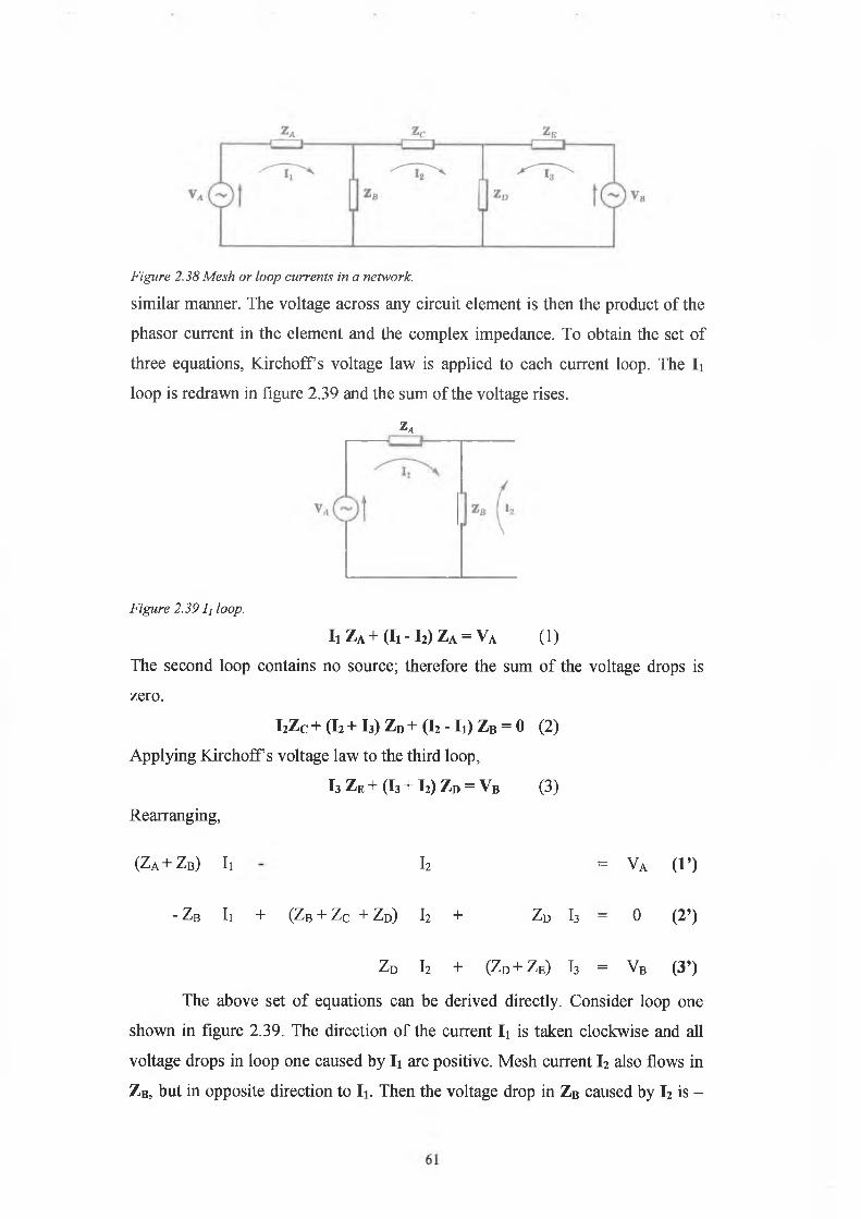
Figure 2.38 Mesh or loop currents in a network.
similar manner. The voltage across any circuit element is then the product of the
phasor current in the element and the complex impedance. To obtain the set of
three equations, Kirchoff s voltage law is applied to each current loop. The Ii
loop is redrawn in figure 2.39 and the sum of the voltage rises.
ZA
Figure 2.39 I t loop.
Ii Za + (I i - I 2)Z a = Va (1)
The second loop contains no source; therefore the sum of the voltage drops is
zero.
\{Lc + (I2 + I3) Zd + (I2 - Ii) Zb = 0 (2)
Applying Kirchoff s voltage law to the third loop,
I3 Ze + (I3+I2)Z d = V b ( 3 )
Rearranging,
(Z a + Z b) Ii h = V a ( ! ’)
- Zb Ii + (Zb + Zq + Zd) h + N a ¿r1 11 0 (2’)
Z D h + (Z D+ Z E) I3 = VB (3’)
The above set of equations can be derived directly. Consider loop one
shown in figure 2.39. The direction of the current Ii is taken clockwise and all
voltage drops in loop one caused by Ii are positive. Mesh current I2 also flows in
ZB, but in opposite direction to Ii. Then the voltage drop in ZB caused by I2 is -
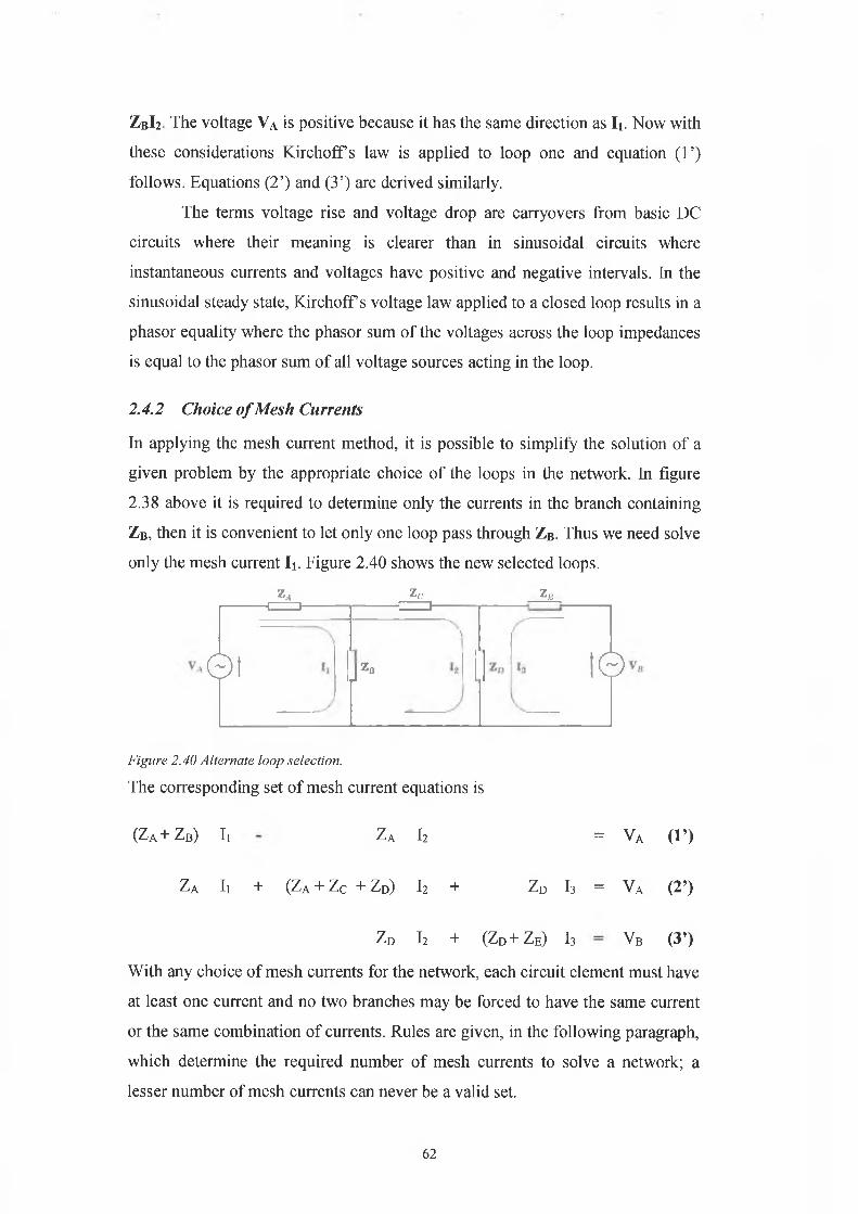
Z B I 2 The voltage Va is positive because it has the same direction as I j . Now with
these considerations Kirchoffs law is applied to loop one and equation (1’)
follows. Equations (2’) and (3’) are derived similarly.
The terms voltage rise and voltage drop are carryovers from basic DC
circuits where their meaning is clearer than in sinusoidal circuits where
instantaneous currents and voltages have positive and negative intervals. In the
sinusoidal steady state, Kirchoffs voltage law applied to a closed loop results in a
phasor equality where the phasor sum of the voltages across the loop impedances
is equal to the phasor sum of all voltage sources acting in the loop.
2.4.2 Choice o f Mesh Currents
In applying the mesh current method, it is possible to simplify the solution of a
given problem by the appropriate choice of the loops in the network. In figure
2.38 above it is required to determine only the currents in the branch containing
Z b , then it is convenient to let only one loop pass through Z b . Thus we need solve
only the mesh current Ii. Figure 2.40 shows the new selected loops.
ZA Zc ZE!----- ( 1----- 1——
<0 1 JZb
'
I©
Figure 2.40 Alternate loop selection.
The corresponding set of mesh current equations is
(Za+ Z b) Ii ZA h = Va (1’)
Z a l i + (Z a + Z c + Z d) I2 + ZD I3 = Va (2’)
Zd I2 + (Zd+Ze) I3 — Vb (3’)
With any choice of mesh currents for the network, each circuit element must have
at least one current and no two branches may be forced to have the same current
or the same combination of currents. Rules are given, in the following paragraph,
which determine the required number of mesh currents to solve a network; a
lesser number of mesh currents can never be a valid set.
62
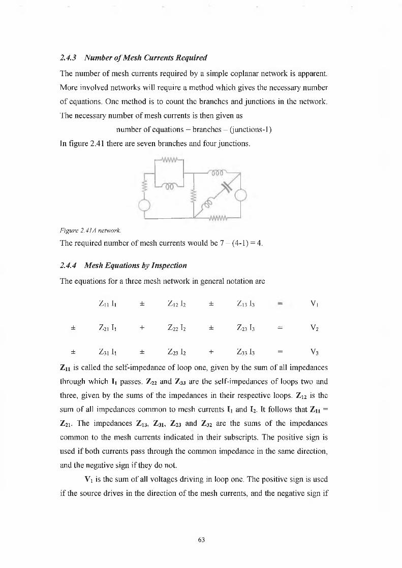
2.4.3 Number o f Mesh Currents Required
The number of mesh currents required by a simple coplanar network is apparent.
More involved networks will require a method which gives the necessary number
of equations. One method is to count the branches and junctions in the network.
The necessary number of mesh currents is then given as
number of equations = branches - (junctions-1)
In figure 2.41 there are seven branches and four junctions.
Figure 2.41 A network.
The required number of mesh currents would be 7 - (4-1) = 4.
2.4.4 Mesh Equations by Inspection
The equations for a three mesh network in general notation are
Znli ± Z12 h ± Zo I3 ~ Vi
± Z 2 1 I i + Z 2 2 1 2 ± Z 2 3 1 3 = V 2
± Z 3 1 I i ± Z 2 3 1 2 + Z 3 3 1 3 = V 3
Zn is called the self-impedance of loop one, given by the sum of all impedances
through which Ii passes. Z22 and Z33 are the self-impedances of loops two and
three, given by the sums of the impedances in their respective loops. Zn is the
sum of all impedances common to mesh currents Ii and h. It follows that Zn =
Z2 1. The impedances Zi3, Z31, Z23 and Z32 are the sums of the impedances
common to the mesh currents indicated in their subscripts. The positive sign is
used if both currents pass through the common impedance in the same direction,
and the negative sign if they do not.
Vi is the sum of all voltages driving in loop one. The positive sign is used
if the source drives in the direction of the mesh currents, and the negative sign if
63
it drives against the mesh current. V2 and V3 are the sums o f the driving voltages
in their respective loops.
2.4.5.1 Matrices
A matrix is a rectangular array of numbers or functions enclosed in a pair of
brackets and is subject to certain rules of operation. In the matrix
A =
a\\ a \2 a\nl 2n
a„ a„
the numbers or functions a. are called its elements. An elementay is in row/' and
column j . This matrix, o fm rows and« columns, is of order “ m x n ’’and is called
“the matrix A”. Two matrices are equal if and only if one is the exact duplicate of
the other.
2.4.5.2 Addition o f Matrices
Two matrices of the same order are conformable for addition or subtraction; two
matrices of different orders cannot be added or subtracted. The sum/difference of
two m x n matrices, A = [aif] and B = [¿iyJ, is the mxn matrix C where each
element of C is the sum/difference of the corresponding elements of A and B .
Thus A ± B = \atj ± btjJ.
2.4.5.3 Multiplication o f Matrices
The product AB , in that order, of the 1 x m matrix A = [au au ... alm] and
the s ix 1 matrix B =
In
is the l x l matrix C :
C = au a12 ... alm • yu^11^11 ^12^21 + a lmbml= Y j axk
k=\'ml
64
Note that each element of the row is multiplied into each corresponding element
of the column and then the products are summed.
Matrix A is conformable to matrix B for multiplication, i.e. the product
AB is defined, only when the number of columns of A is equal to the number of
rows of B . Thus if A is a 3 x 2 matrix and B is a 2 x 5 matrix, then the product
AB is defined but the product BA is not defined. If D is a 3x3 and E is a 3 x 3
matrix, both products AB and BA are defined.
2.4.5.4 Inversion
In an arrangement of positive integers, an inversion exists when a larger integer
precedes a smaller integer. For example, in 132 the integer 3 precedes 1; hence
there are 3 inversions. In 4213 the integer 4 precedes 2, 1 and 3, and the integer 2
precedes 1; thus there are 4 inversions. In 3421 the integer 3 precedes 2 and 1, the
integer 4 precedes 2 and 1, and the integer 2 precedes 1; thus there are 5
inversions.
2.4.5.5 Determinant o f a Square Matrix
Let us take n elements of the «-square matrix
a\\ ®\2 "• a\n_ <?21 a22 ■■■ a2n
_®n\ ®n2
and form a product a {/] a2ji ... aAu such that one and only one element
belongs to any row and one element belongs to any column. Note that the
sequence of first subscripts is, for convenience, in the order 1, 2, ..., n; then the
sequence j i , j 2,---,jn of second subscripts is one of the «! permutations of the
integers 1, 2, ..., n. Associate a + or - sign with the product according to the
number of inversions of the second subscripts is even or odd. Then the
determinant of and «-square matrix A , written \A\, is the sum of all «! such
different signed products which can be formed from the elements of A . The
determinant of a square matrix of order « is called a determinant of order n.
65
The value of the determinant \A\ of order n is the sum of the n products
obtained by multiplying each element of any chosen row/column of \A\ by its
cofactor. Thus
“ n « 12 «13
M = a2] « 2 2 « 2 3 — ai2A12 + a22&22 « 3 2 ^ 3 2
« 3 1 « 3 2 « 3 3
«2 1 « 2 3+ Cl 22
«11 «13 «11 «13« 1 2 « 3 2
«31 « 3 3 «3 1 « 3 3 «2 1 « 2 3
is the expansion \A\ along the second column.
2.4.5.6 Solution o f Linear Equations by Determinant and Cramer’s Rule
The system of three linear equations in three unknowns jti, xi, X3
« 1 1 * 1 + «12 x2 + « 1 3 * 3 = k,a2Xxx + d22x2 + « 2 3 * 3 — k2
« 3 1 *1 + « 3 2 * 2 + a33x3 11
UJ
may be written in matrix form as
1js «12 «13
1 i 11
«21 « 2 2 #23 * 2 = k 2
_ « 3 I «32 ^33 _. * 3 . > 3 .
The numerical value of the coefficient determinant, Aa, is multiplied by x\ if each
element of the first column is multiplied by x\
«11 «1 2 «13 « 11*1 « 12 «13
II<
« 2 1 « 2 2 « 2 3 and = « 21*1 « 2 2 « 2 3
«3 1 « 3 2 « 3 3 « 3 1 * 1 « 3 2 « 3 3
Now to each element of the first column of the last determinant add x% times the
corresponding element of the second column and X3 times the corresponding
element of the third column. Then
( « n X j + a l2x2 + a 13jc3) « 1 2 «13 K « 1 2 «13
* A = (¿3t2i *1 + < ^ 2 2 * 2 " ^ « 23* 3 ) « 2 2 « 2 3= k2 « 2 2 « 2 3
( « 3 1 * 1 + # 3 2 * 2 ‘*‘ « 33* 3 ) « 3 2 « 3 3 K « 3 2 « 3 3
66
provided Aa ^ 0. Similarly,
x2 =
kx a i2 a nk2 a 22 <*23
a31 a 33X] ~ Aa
y,
«ii K aX3 au « 1 2 K21 k2 a n « 2 1 a21 k2
f l 31 k3 a33- x, = -a 3\ a 32 k3
This method of solution, called Cramer’s Rule, can be applied to any system of n
linear equations in n unknowns provided the coefficient’s determinant is not zero.
2.4.6.1 Matrix Methods and Circuit Analysis
The three mesh current equations
Z n l 1 ± Z 1212 Z \3 I3 Vi
± Z21 Ii + Z22 I2 Z23 I3 = V2
± Z 3 1 I 1 ± Z2312 + Z33 I3 V3
are now written in matrix form
" Zn ±Z 12 ±Z |3I ' ' ] \ V'1
± Z 2I Z22 ± z 23 = n ° r [ z I / ] = M
A Z31 ± z 32Z 33 . J i .
referred to as the matrix form of Ohm’s law, were [z] is the impedance matrix,
[/] the current matrix and [v] the voltage matrix.
The mesh currents , I 2 and I 3 are found as the ratios of the two
determinants:
K + Z 12 ± Z „ Z n ±zl3 Zn <N
N+1 Kr2 Z 22 ± Z 23 ± Z 21 2 ±Z23 ±z21 Z 22 v*V3 ± Z 32 Z 33
■ L~ + Z 31 V3 Z33 h=-— Z 3i — Z 32 V3
67
When the numerator determinant of each is expanded about the elements of the
column containing the voltages, we obtain the following set of equations for the
mesh currents:
+ K *21 KV z /
31
V z y
V ^ Z J
f A >
13vAz y
+ K
+ K
22 V,\ Z /
23
*32
V 2 J
33
(1)
(2)
(3)\ 2 J V Z J
The terms on the right sides of equations (1), (2) and (3) are phasor components
which result from the various driving voltages. Thus in (1) the mesh current I x
consists of three parts: F1(a11/A z) due to driving voltage V{, F2(A21/A z)due to
driving voltage V2, and V3 (A31 / A J due to driving voltage V3.
2.4.6.2 Driving Point Impedance
Consider a passive or source-free network with two external connections as
shown in the figure 2.42. Apply a voltage source V: and call the resulting mesh
Multi-mesh Passive
Network
Figure 2.42 Multi-mesh passive network with attached voltage source.
current Ix. Since there are no other sources in the network the equation for mesh
current Ix is
An+ (0) 21 + (0 1 ^ + ... = K A„
V ^ y
The input or driving point impedance is the ratio of the applied voltage V: to the
resulting current I x. Thus
2 , ^ , / A = A ,/A „
The input impedance of an active network is defined as the impedance presented
by the network to the specified terminals when all internal sources are shorted
but their internal impedances are retained. Thus the ratio Az/A u is the driving
68
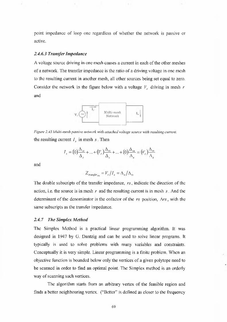
point impedance of loop one regardless of whether the network is passive or
active.
2.4.6.3 Transfer Impedance
A voltage source driving in one mesh causes a current in each of the other meshes
of a network. The transfer impedance is the ratio of a driving voltage in one mesh
to the resulting current in another mesh, all other sources being set equal to zero.
Consider the network in the figure below with a voltage Vr driving in mesh r
and
Figure 2.43 Multi-mesh passive network with attached voltage source with resulting current.
the resulting current Is in mesh s . Then
The double subscripts of the transfer impedance, rs , indicate the direction of the
action, i.e. the source is in mesh r and the resulting current is in mesh s . And the
determinant of the denominator is the cofactor of the rs position, A r s , with the
same subscripts as the transfer impedance.
2.4.7 The Simplex Method
The Simplex Method is a practical linear programming algorithm. It was
designed in 1947 by G. Dantzig and can be used to solve linear programs. It
typically is used to solve problems with many variables and constraints.
Conceptually it is very simple. Linear programming is a finite problem. When an
objective function is bounded below only the vertices of a given polytope need to
be scanned in order to find an optimal point. The Simplex method is an orderly
way of scanning such vertices.
The algorithm starts from an arbitrary vertex of the feasible region and
finds a better neighbouring vertex. (“Better” is defined as closer to the frequency
Multi-meshNetwork
Is = (o)— + - + (K )— +... + ( 0 )^ - = (KA, A, w A, A
and
69
sweep, in our case). If no neighbouring vertex is “better”, the current vertex can
be proven globally optimal. For a more in depth explanation of the Simplex
Method refer to reference [8],
70
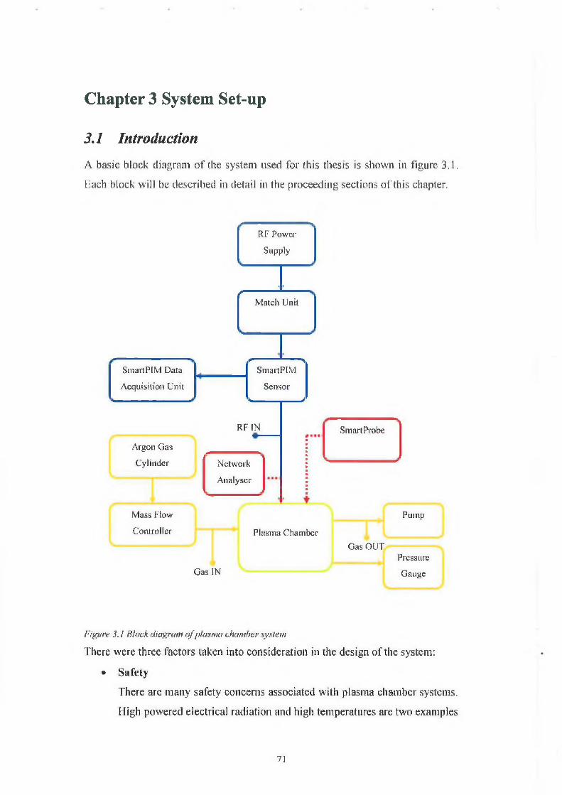
Chapter 3 System Set-up
3.1 Introduction
A basic block diagram of the system used for this thesis is shown in figure 3.1.
Each block will be described in detail in the proceeding sections of this chapter.
RF Power
Supply
\rt
M atch Unit
SmartPIM Datat \
SmartPIM
Acquisition Unit Sensor 1 ^
RF IN
Argon Gas
Cylinder Network
Analyser
Smart Probe
M ass Flow Pump
Controller Plasm a Cham ber
Gas OUT
G as IN
Pressure
Gauge
Figure 3.1 Block diagram o f plasma chamber system
There were three factors taken into consideration in the design of the system:
• Safety
There are many safety concerns associated with plasma chamber systems.
High powered electrical radiation and high temperatures are two examples
71
of hazardous energies present. Different gases are used to generate
plasmas in the chamber. Only argon and nitrogen are used in this system
as they are not combustible. However they still are hazardous as they can
cause asphyxiation. Ergonomic safety issues are also a major concern.
Parts of the system such as the radio frequency generator and gas
cylinders are very heavy and should not be carried.
These are just some of the safety issues that must be addressed in
the design of a plasma chamber system. By employing proper safety
measures, the risk of injury will be greatly reduced. This is a key element
in the design of any hazardous system.
• Cost
There was a limited budget for the design of this system. There is no point
in building a system that will cost too much to maintain anytime
something fails. The engineer should always balance between
performance and cost. The system will have to achieve a definite
specification. If the system operates at a much better specification than
required but cost has been compromised to achieve this then the system is
of poor design. Safety must never be compromised for cost.
• Performance
It is essential that a plasma chamber system has a stable performance,
otherwise repeatable and reproducible measurements cannot be taken.
Conclusions about experiments cannot be made as the data taken from the
system cannot be trusted. It is important that any data from an experiment
can be reproduced. The performance of the experiment should match its
initial performance if the experiment is set up, as per a given
specification, in any other laboratory.
3.2 System Components
3.2.1 The Power Supply
The power supply used was an Advanced Energy RF Power Delivery System,
model number RFX-600. It is capable of driving a single frequency signal of
13.56 MHz within the range of 6 to 600 Watts into a 50 Q load. A typical power
72
range of between 10 Watts and 150 Watts was used for driving the plasma in the
chamber.
3.2.2 The Network Analyser
The HP 8753D network analyser was used for collecting data from the plasma
chamber system. It is a high performance vector network analyser for laboratory
or production measurements of reflection and transmission parameters. It
integrates a high resolution synthesised RF source, an S-parameter test set and a
dual channel three-input receiver to measure and display magnitude, phase and
group delay responses of active and passive RF networks.
3.2.3 The Plasma Chamber
A capacitively coupled plasma chamber was designed for this work (refer to §
2.3.3 RF Diodes). A mechanically similar design was used for the grounded
electrode and the RF-live electrode. Copper sheets, pipes, rods and finger-strip
were used for the conducting parts of the electrodes. PTFE was used for the
insulating parts of the electrodes. Figures 3.2 through 3.11 illustrate the assembly
of the grounded electrode. The RF-live electrode is assembled in the same
manner. An N-type (female) QC connector is also attached to the RF-live
electrode. N-type (male) transmission line cables are connected from here to the
power generator via the matching unit.
A minimum stand-off distance of 10mm through PTFE and vacuum was
observed between RF-live components and grounded components. This
precaution was taken to stop dielectric breakdown and hence shorting between
RF-live and grounded components.
It was desired to contain the plasma between the two electrode plates, thus
achieving the RF diode setup as described in § 2.3.3. The shield in the electrode,
shown in figure 3.4, stops electromagnetic radiation from the electrode plates
permeating into the cavity behind the electrode assembly. As a result, gas present
here will not be excited into the plasma state. Plasma only forms between the two
electrode plates shown in figure 3.11.
73
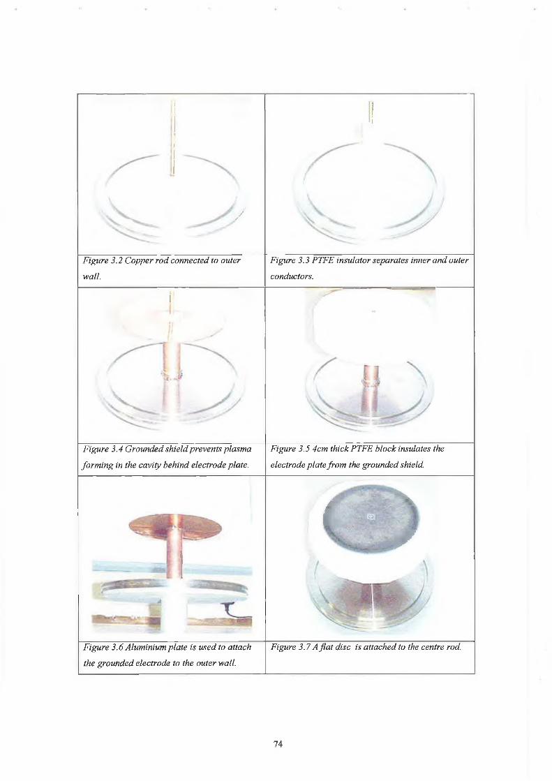
/
Figure 3.2 Copper rod connected to outer
wall.
Figure 3.3 PTFE insulator separates inner and outer
conductors.
I
Figure 3.4 Grounded shield prevents plasma
forming in the cavity behind electrode plate.
Figure 3.5 4cm thick PTFE block insulates the
electrode plate from the grounded shield.
Vc
(tC, >,CD J
w
Figure 3.6 Aluminium plate is used to attach
the grounded electrode to the outer wall.
Figure 3.7 A fla t disc is attached to the centre rod.
74
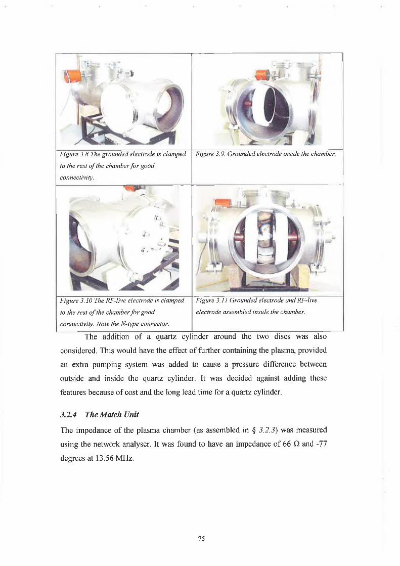
Figure 3.8 The grounded electrode is clamped
to the rest o f the chamber fo r good
connectivity.
Figure 3.9. Grounded electrode inside the chamber
Figure 3.10 The RF-live electrode is clamped Figure 3.11 Grounded electrode and RF-live
to the rest o f the chamber fo r good electrode assembled inside the chamber,
connectivity. Note the N-type connector.
The addition of a quartz cylinder around the two discs was also
considered. This would have the effect of further containing the plasma, provided
an extra pumping system was added to cause a pressure difference between
outside and inside the quartz cylinder. It was decided against adding these
features because of cost and the long lead time for a quartz cylinder.
3.2.4 The Match Unit
The impedance of the plasma chamber (as assembled in § 3.2.3) was measured
using the network analyser. It was found to have an impedance of 66 Q. and -77
degrees at 13.56 MHz.
75
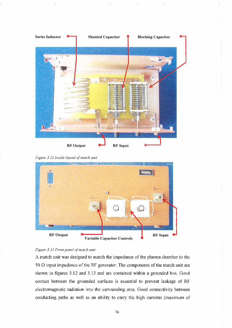
Figure 3.12 Inside layout o f match unit
Figure 3.13 Front panel o f match unit
A match unit was designed to match the impedance of the plasma chamber to the
50 Q input impedance of the RF generator. The components of the match unit are
shown in figures 3.12 and 3.13 and are contained within a grounded box. Good
contact between the grounded surfaces is essential to prevent leakage of RF
electromagnetic radiation into the surrounding area. Good connectivity between
conducting paths as well as an ability to carry the high currents (maximum of
76
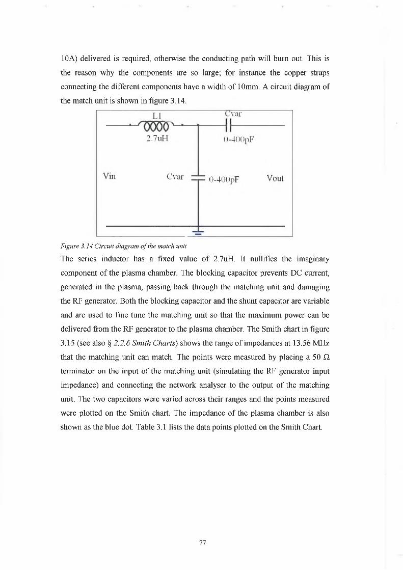
10A) delivered is required, otherwise the conducting path will burn out. This is
the reason why the components are so large; for instance the copper straps
connecting the different components have a width of 1 Omm. A circuit diagram of
the match unit is shown in figure 3.14.
Figure 3.14 Circuit diagram o f the match unit
The series inductor has a fixed value of 2.7uH. It nullifies the imaginary
component of the plasma chamber. The blocking capacitor prevents DC current,
generated in the plasma, passing back through the matching unit and damaging
the RF generator. Both the blocking capacitor and the shunt capacitor are variable
and are used to fine tune the matching unit so that the maximum power can be
delivered from the RF generator to the plasma chamber. The Smith chart in figure
3.15 (see also § 2.2.6 Smith Charts) shows the range of impedances at 13.56 MHz
that the matching unit can match. The points were measured by placing a 50 D.
terminator on the input of the matching unit (simulating the RF generator input
impedance) and connecting the network analyser to the output of the matching
unit. The two capacitors were varied across their ranges and the points measured
were plotted on the Smith chart. The impedance of the plasma chamber is also
shown as the blue dot. Table 3.1 lists the data points plotted on the Smith Chart.
77
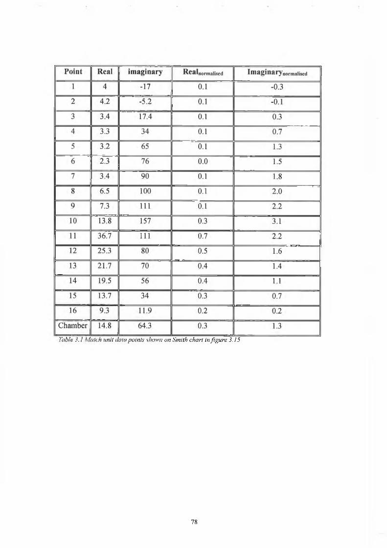
Table 3 .1 Match unit data points shown on Smith chart in figure 3.15
78
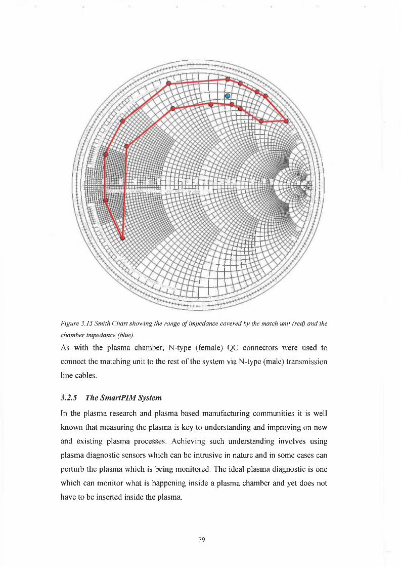
Figure 3.15 Smith Chart showing the range o f impedance covered by the match unit (red) and the
chamber impedance (blue).
As with the plasma chamber, N-type (female) QC connectors were used to
connect the matching unit to the rest of the system via N-type (male) transmission
line cables.
3.2.5 The Smart PIM System
In the plasma research and plasma based manufacturing communities it is well
known that measuring the plasma is key to understanding and improving on new
and existing plasma processes. Achieving such understanding involves using
plasma diagnostic sensors which can be intrusive in nature and in some cases can
perturb the plasma which is being monitored. The ideal plasma diagnostic is one
which can monitor what is happening inside a plasma chamber and yet does not
have to be inserted inside the plasma.
79
SmartPIM™, Scientific Systems Plasma Impedance Monitor is such a
non-intrusive plasma diagnostic. It resides on the RF power line post match unit.
SmartPIM™ measures the plasma impedance at the fundamental frequency and
the four higher harmonics. The SmartPIM™ system comprises an acquisition
electronics unit, RF transmission line sensor and PIMSoft™ software.
Communication between the acquisition electronics unit and PIMSoft™ is via
RS232. PIMSoft™ is used to acquire and display the current, voltage and phase
of the fundamental and four higher harmonics. Power and impedance are then
calculated from the current, voltage and phase values.
3.2.6 The SmartProbe
SmartProbe™ from Scientific Systems is a commercial Langmuir probe system
and is used to measure a wide range of plasma parameters such as plasma
density, uniformity and electron temperature distribution. It enables plasma
researchers to understand the complexity and characteristics of a plasma and how
they relate to the plasma process they are trying to develop. SmartSoft™, the
software application that comes packaged with the SmartProbe™, is a powerful
Microsoft Windows compatible software package that provides immediate data
acquisition and analysis.
3.3.1 Mechanical Systems
An Edwards, 2-stage, 12 litre pump was used to bring the chamber down to
vacuum. Edward Pre-lOk pressure gauges were used to monitor the pressure
within the chamber. A Spectra Vascan Plus chemical detector was used to find
leaks in the chamber. A Tylan Mass Flow controller was used to set the flow of
gas into the plasma chamber.
80
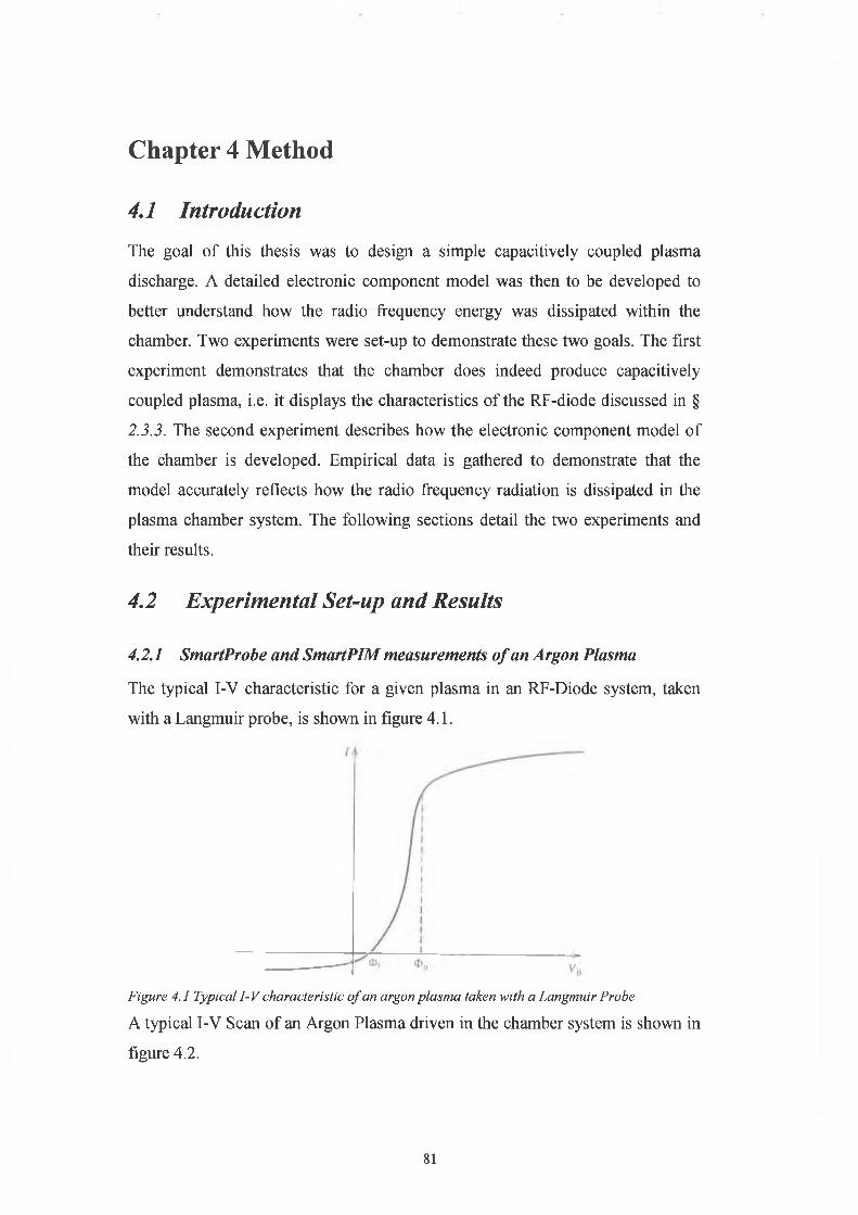
Chapter 4 Method
4.1 Introdu ction
The goal of this thesis was to design a simple capacitively coupled plasma
discharge. A detailed electronic component model was then to be developed to
better understand how the radio frequency energy was dissipated within the
chamber. Two experiments were set-up to demonstrate these two goals. The first
experiment demonstrates that the chamber does indeed produce capacitively
coupled plasma, i.e. it displays the characteristics of the RF-diode discussed in §
2.3.3. The second experiment describes how the electronic component model of
the chamber is developed. Empirical data is gathered to demonstrate that the
model accurately reflects how the radio frequency radiation is dissipated in the
plasma chamber system. The following sections detail the two experiments and
their results.
4.2 Experimental Set-up and Results
4.2.1 SmartProbe and SmartPIM measurements o f an Argon Plasma
The typical I-V characteristic for a given plasma in an RF-Diode system, taken
with a Langmuir probe, is shown in figure 4.1.
Figure 4.1 Typical I- V characteristic o f an argon plasma taken with a Langmuir Probe
A typical I-V Scan of an Argon Plasma driven in the chamber system is shown in
figure 4.2.
81
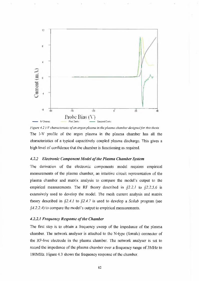
12
8
A
■p
P -A
O
Probe Bias (V)— IVCharac — — First Deriv. -------- Second Deriv
Figure 4 .21-V characteristic o f an argon plasma in the plasma chamber designed fo r this thesis
The I-V profile of the argon plasma in the plasma chamber has all the
characteristics of a typical capacitively coupled plasma discharge. This gives a
high level of confidence that the chamber is functioning as required.
4.2.2 Electronic Component Model o f the Plasma Chamber System
The derivation of the electronic components model requires empirical
measurements of the plasma chamber, an intuitive circuit representation of the
plasma chamber and matrix analysis to compare the model’s output to the
empirical measurements. The RF theory described in §2.2.1 to §2.2.5.6 is
extensively used to develop the model. The mesh current analysis and matrix
theory described in §2.4.1 to §2.4.7 is used to develop a Scilab program (see
§4.2.2.4) to compare the model’s output to empirical measurements.
4.2.2.1 Frequency Response o f the Chamber
The first step is to obtain a frequency sweep of the impedance of the plasma
chamber. The network analyser is attached to the N-type (female) connector of
the RF-live electrode in the plasma chamber. The network analyser is set to
record the impedance of the plasma chamber over a frequency range of 3MHz to
180MHz. Figure 4.3 shows the frequency response of the chamber.
82
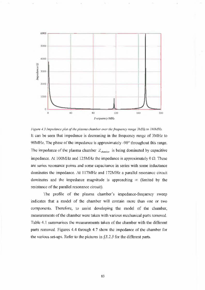
6000
Frequency/MHz
Figure 4.3 Impedance plot o f the plasma chamber over the frequency range 3MHz to I80MHz.
It can be seen that impedance is decreasing in the frequency range of 3MHz to
90MHz. The phase of the impedance is approximately -90° throughout this range.
The impedance of the plasma chamber Zchamber is being dominated by capacitive
impedance. At 100MHz and 125MHz the impedance is approximately 0 i l These
are series resonance points and some capacitance in series with some inductance
dominates the impedance. At 117MHz and 172MHz a parallel resonance circuit
dominates and the impedance magnitude is approaching qo (limited by the
resistance of the parallel resonance circuit).
The profile of the plasma chamber’s impedance-frequency sweep
indicates that a model of the chamber will contain more than one or two
components. Therefore, to assist developing the model of the chamber,
measurements of the chamber were taken with various mechanical parts removed.
Table 4.1 summarises the measurements taken of the chamber with the different
parts removed. Figures 4.4 through 4.7 show the impedance of the chamber for
the various set-ups. Refer to the pictures in §3.2.3 for the different parts.
83
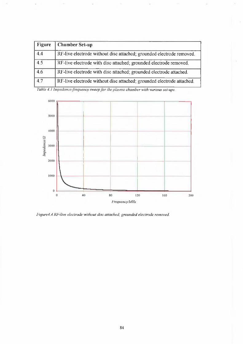
Figure Chamber Set-up
4.4 RF-live electrode without disc attached; grounded electrode removed.
4.5 RF-live electrode with disc attached; grounded electrode removed.
4.6 RF-live electrode with disc attached; grounded electrode attached.
4.7 RF-live electrode without disc attached; grounded electrode attached.
Table 4.1 Impedance-frequency sweep for the plasma chamber with various set-ups.
Frequency/MHz
Figure4.4 RF-live electrode without disc attached; grounded electrode removed.
84
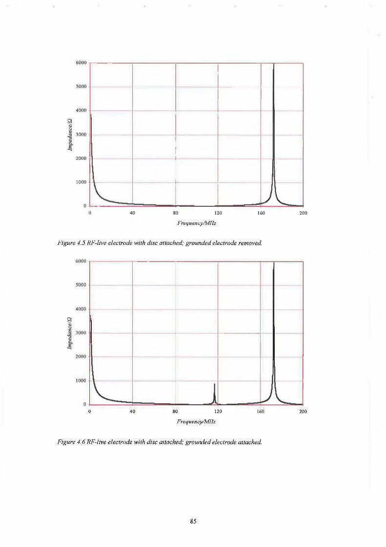
Frequency/MHz
Figure 4.5 RF-live electrode with disc attached; grounded electrode removed.
0 40 80 120 160 200
Frequency/MHz
Figure 4.6 RF-live electrode with disc attached; grounded electrode attached.
85
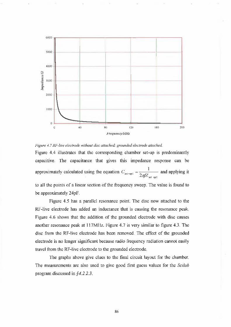
6000
5000
4000
0 40 80 120 160 200
Frequency/MHz
Figure 4.7 RF-live electrode without disc attached; grounded electrode attached.
Figure 4.4 illustrates that the corresponding chamber set-up is predominantly
capacitive. The capacitance that gives this impedance response can be
approximately calculated using the equation Cset_upl ------- ------- and applying it1 r f Z Set-u p \
to all the points of a linear section of the frequency sweep. The value is found to
be approximately 24pF.
Figure 4.5 has a parallel resonance point. The disc now attached to the
RF-live electrode has added an inductance that is causing the resonance peak.
Figure 4.6 shows that the addition of the grounded electrode with disc causes
another resonance peak at 117MHz. Figure 4.7 is very similar to figure 4.3. The
disc from the RF-live electrode has been removed. The effect of the grounded
electrode is no longer significant because radio frequency radiation cannot easily
travel from the RF-live electrode to the grounded electrode.
The graphs above give clues to the final circuit layout for the chamber.
The measurements are also used to give good first guess values for the Scilab
program discussed in §4.2.2.3.
86
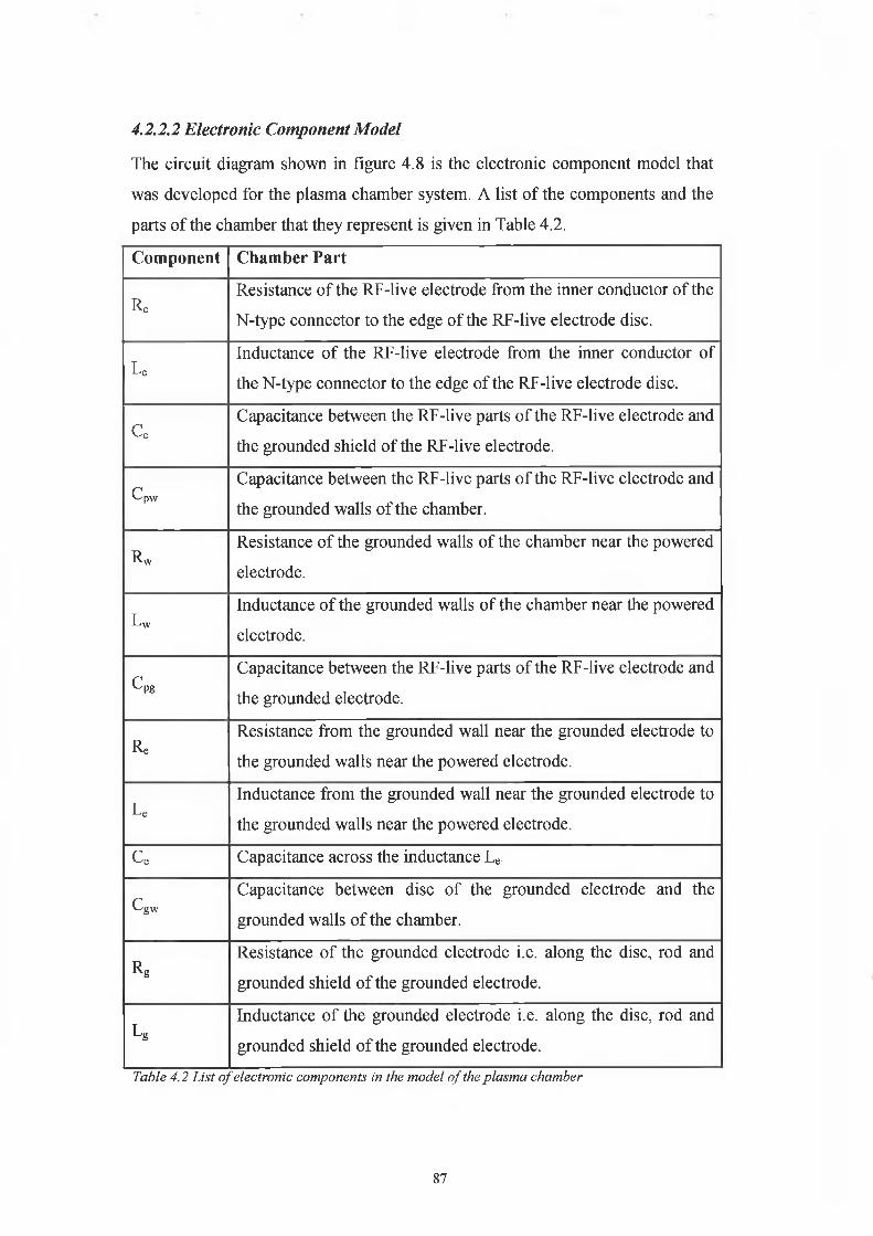
4.2.2.2 Electronic Component Model
The circuit diagram shown in figure 4.8 is the electronic component model that
was developed for the plasma chamber system. A list of the components and the
parts of the chamber that they represent is given in Table 4.2.
Component Chamber Part
RcResistance of the RF-live electrode from the inner conductor of the
N-type connector to the edge of the RF-live electrode disc.
LcInductance of the RF-live electrode from the inner conductor of
the N-type connector to the edge of the RF-live electrode disc.
CoCapacitance between the RF-live parts of the RF-live electrode and
the grounded shield of the RF-live electrode.
cp\vCapacitance between the RF-live parts of the RF-live electrode and
the grounded walls of the chamber.
RwResistance of the grounded walls of the chamber near the powered
electrode.
LwInductance of the grounded walls of the chamber near the powered
electrode.
CpgCapacitance between the RF-live parts of the RF-live electrode and
the grounded electrode.
RcResistance from the grounded wall near the grounded electrode to
the grounded walls near the powered electrode.
LeInductance from the grounded wall near the grounded electrode to
the grounded walls near the powered electrode.
c e Capacitance across the inductance Le.
CgwCapacitance between disc of the grounded electrode and the
grounded walls of the chamber.
RgResistance of the grounded electrode i.e. along the disc, rod and
grounded shield of the grounded electrode.
LgInductance of the grounded electrode i.e. along the disc, rod and
grounded shield of the grounded electrode.
Table 4.2 List o f electronic components in the model o f the plasma chamber
87
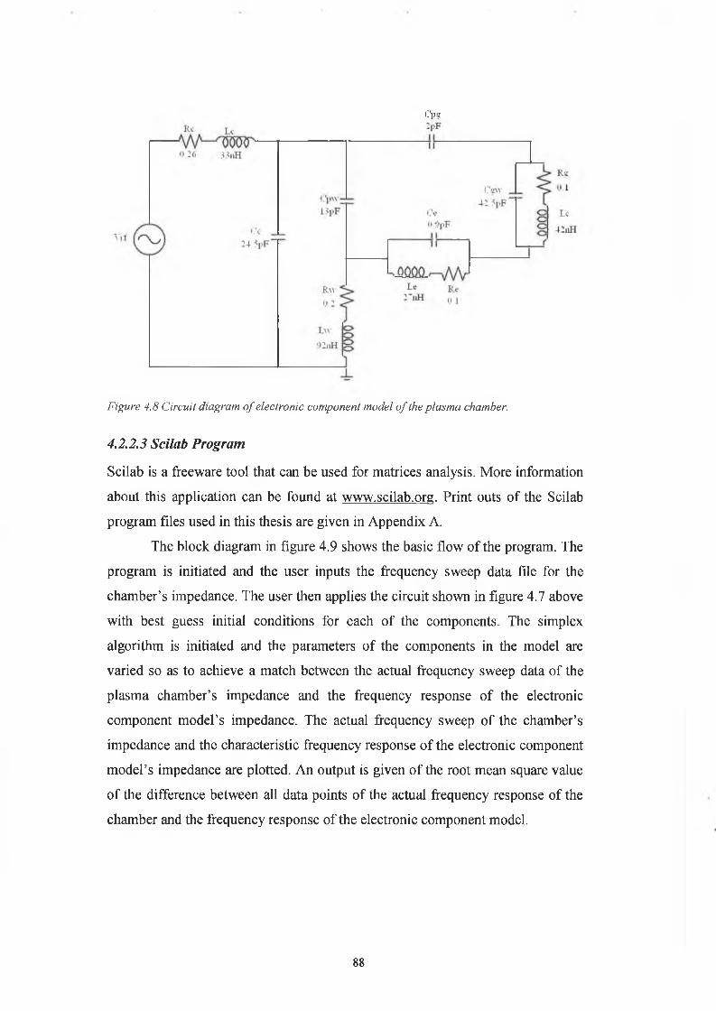
Cp?
Figure 4.8 Circuit diagram o f electronic component model o f the plasma chamber.
4.2.2.3 Scilab Program
Scilab is a freeware tool that can be used for matrices analysis. More information
about this application can be found at www.scilab.org. Print outs of the Scilab
program files used in this thesis are given in Appendix A.
The block diagram in figure 4.9 shows the basic flow of the program. The
program is initiated and the user inputs the frequency sweep data file for the
chamber’s impedance. The user then applies the circuit shown in figure 4.7 above
with best guess initial conditions for each of the components. The simplex
algorithm is initiated and the parameters of the components in the model are
varied so as to achieve a match between the actual frequency sweep data of the
plasma chamber’s impedance and the frequency response of the electronic
component model’s impedance. The actual frequency sweep of the chamber’s
impedance and the characteristic frequency response of the electronic component
model’s impedance are plotted. An output is given of the root mean square value
of the difference between all data points of the actual frequency response of the
chamber and the frequency response of the electronic component model.
88
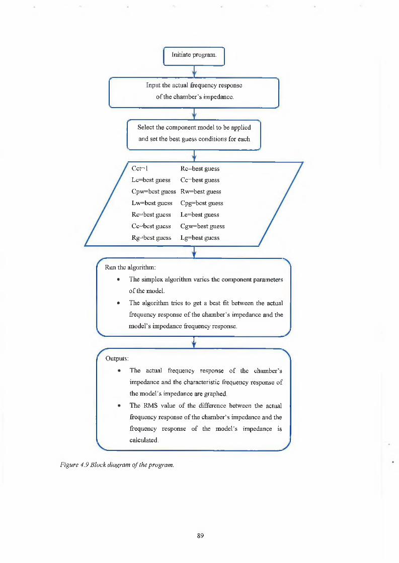
Initiate program.
Input the actual frequency response
o f the chamber’s impedance.
Select the component model to be applied
and set the best guess conditions for each
C ct= l Rc=best guess
Lc=best guess Cc=best guess
Cpw=best guess Rw=best guess
Lw=best guess Cpg=best guess
Re=best guess Le=best guess
Ce=best guess Cgw=best guess
Rg=best guess Lg=best guess
Run the algorithm:
• The simplex algorithm varies the component parameters
o f the model.
• The algorithm tries to get a best fit between the actual
frequency response o f the chamber’s impedance and the
m odel’s impedance frequency response.
Outputs:
The actual frequency response o f the chamber’s
impedance and the characteristic frequency response o f
the model’s impedance are graphed.
The RMS value o f the difference between the actual
frequency response o f the chamber‘s impedance and the
frequency response o f the model’s impedance is
calculated.
Figure 4.9 Block diagram o f the program.
89
Chapter 5 Results and Conclusions
5.1 Introduction
The results generated from the experiments run in chapter 4 are given in chapter
5. Conclusions are drawn and ideas for further experimental work are discussed.
Finally, a synopsis is given of the applications of the work in this thesis for the
semiconductor microchip manufacturing processes.
5.2 SmartProbe Analysis o f the Plasma Chamber
A comparison of figure 4.1 (a typical I-Y characteristic scan of an argon plasma)
and 4.2 (I-Y characteristic of the argon plasma the chamber designed for this
thesis) indicates that the plasma discharge is demonstrating the characteristics of
a capacitively coupled rf discharge. The probe bias voltage Vb is approximately
the same as the plasma potential <X>P (see figure 4.2) at Vb - 26 Volts. The probe
is mainly drawing current from the mobile electrons in the plasma and this is
designated by a positive current flow from the probe to the plasma. As the probe
voltage increases above 26 Volts the current starts to saturate at the electron
saturation current. However, due to the probe geometry, the effective collection
area is increasing as VB is increasing and therefore the current still increases. This
is different to the typical I-V characteristic shown in figure 4 .1 where the current
levels off as the probe bias voltage increases.
As the probe bias voltage decreases below 26 Volts electrons start to be
repelled as per the Boltzmann relation,
ne = nQe~m ,i.e. electrons are attracted to more positive areas of potential. The total current
equals zero when the probe is sufficiently negative with respect to the plasma
such that the electron current is equal to the ion current. The voltage that this
occurs at is called the floating potential Of, and from figure 4.2 it can be seen that
this is at 16 volts for the given argon plasma. At this potential the probe cannot
draw current and therefore floats. As the probe bias voltage is decreased further
ion current increases, leading to ion saturation current. The ion saturation current
90
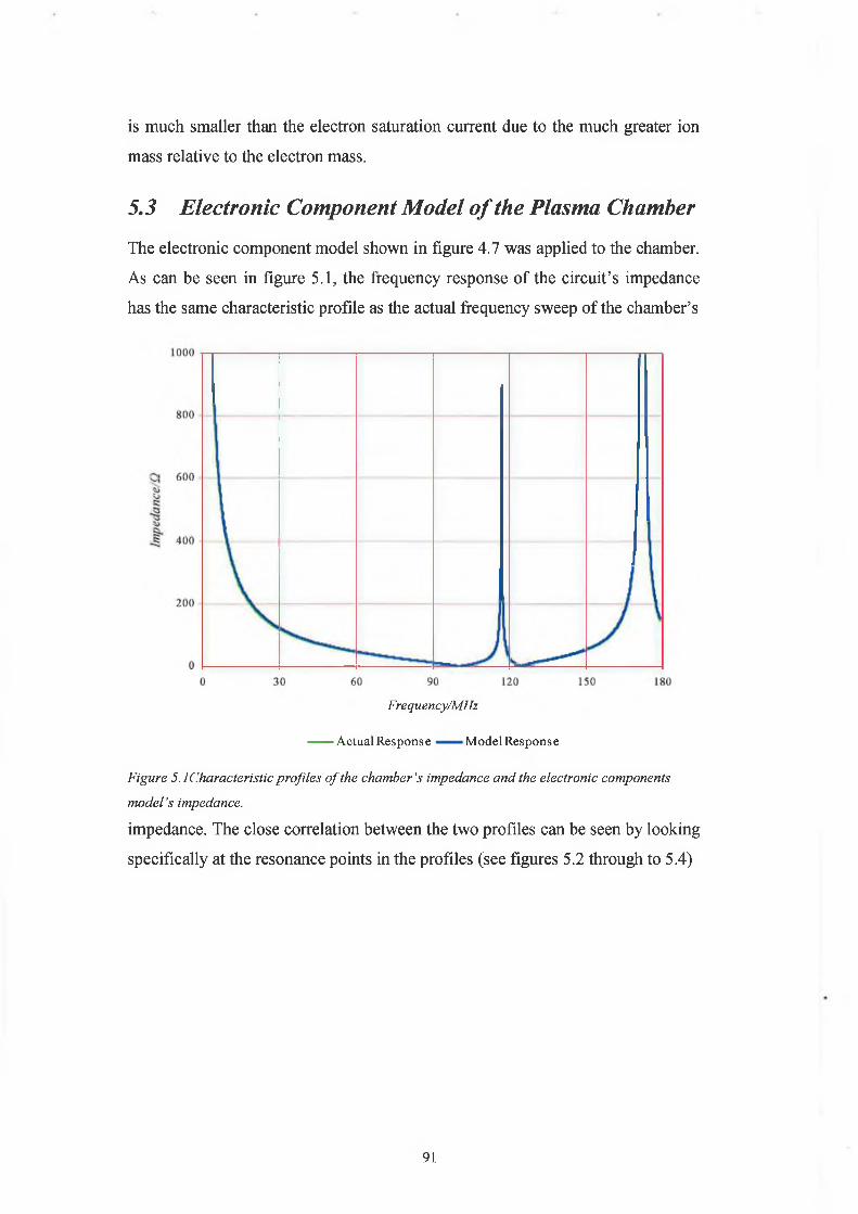
is much smaller than the electron saturation current due to the much greater ion
mass relative to the electron mass.
5.5 Electronic Component Model o f the Plasma Chamber
The electronic component model shown in figure 4.7 was applied to the chamber.
As can be seen in figure 5.1, the frequency response of the circuit’s impedance
has the same characteristic profile as the actual frequency sweep of the chamber’s
Frequency/MHz
------ Actual Response M odel Response
Figure 5. ¡Characteristic profiles o f the chamber's impedance and the electronic components
model’s impedance.
impedance. The close correlation between the two profiles can be seen by looking
specifically at the resonance points in the profiles (see figures 5.2 through to 5.4)
91
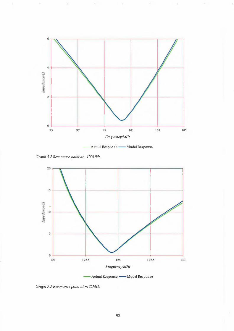
Frequency/MHz
------ Actual R esponse M odel Response
Graph 5.2 Resonance point at ~lOOMHz
Frequency/MHz
A ctual Response M odel Response
Graph 5.3 Resonance point at ~125MHz
92
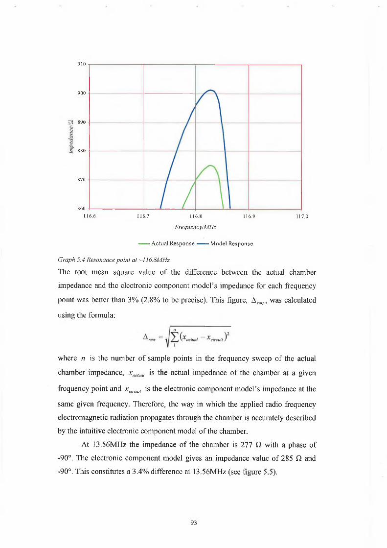
910
s<-S 880
C! 890
900
860
870
116.6 116.7 116.8 116.9 117.0
Frequency/MHz
------ Actual Response — M odel Response
Graph 5.4 Resonance point at ~116.8MHz
The root mean square value of the difference between the actual chamber
impedance and the electronic component model’s impedance for each frequency
point was better than 3% (2.8% to be precise). This figure, Arms, was calculated
using the formula:
where n is the number of sample points in the frequency sweep of the actual
chamber impedance, xachml is the actual impedance of the chamber at a given
frequency point and xcjrcuit is the electronic component model’s impedance at the
same given frequency. Therefore, the way in which the applied radio frequency
electromagnetic radiation propagates through the chamber is accurately described
by the intuitive electronic component model of the chamber.
At 13.56MHz the impedance of the chamber is 277 i2 with a phase of
-90°. The electronic component model gives an impedance value of 285 Q and
-90°. This constitutes a 3.4% difference at 13.56MHz (see figure 5.5).
93
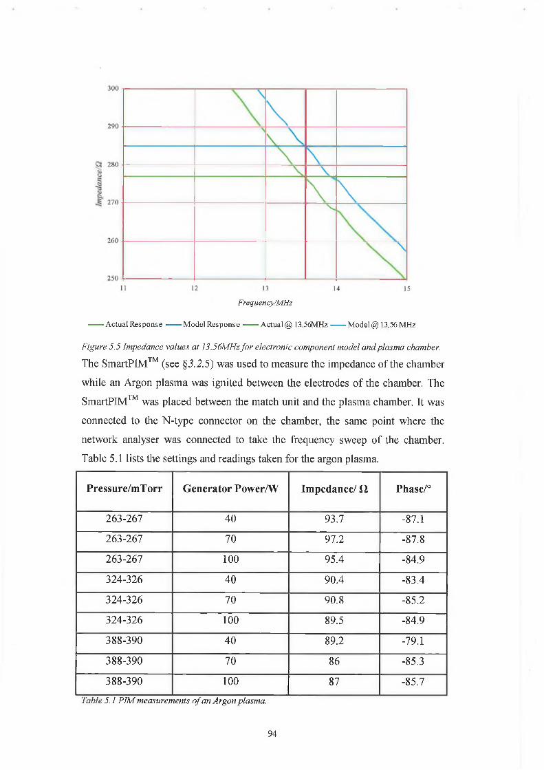
F req u en c y /M H z
------Actual R esponse------ M odelR esponse------ Actual@ 13 56MHz------ Model@ 13.56 MHz
Figure 5.5 Impedance values at 13.56MHz fo r electronic component model and plasma chamber.
The SmartPIM™ (see §3.2.5) was used to measure the impedance of the chamber
while an Argon plasma was ignited between the electrodes of the chamber. The
SmartPIM™ was placed between the match unit and the plasma chamber. It was
connected to the N-type connector on the chamber, the same point where the
network analyser was connected to take the frequency sweep of the chamber.
Table 5.1 lists the settings and readings taken for the argon plasma.
Pressure/mTorr Generator Power/W Impedance/ Q Phase/0
263-267 40 93.7 -87.1
263-267 70 97.2 -87.8
263-267 1 0 0 95.4 -84.9
324-326 40 90.4 -83.4
324-326 70 90.8 -85.2
324-326 1 0 0 89.5 -84.9
388-390 40 89.2 -79.1
388-390 70 86 -85.3
388-390 1 0 0 87 -85.7
Table 5.1 PIM measurements o f an Argon plasma.
94
Figures 5.6 and 5.7 show the variation in impedance and phase as measured by
the SmartPIM™ for the different settings.
Power/Watt
---263-267 --- 324-326 --- 388-390
5.6 Impedance o f Argon Plasma versus generator power.
------263-267 ------ 324-326 -------388-390
5.7 Phase versus power fo r argon plasma.
If the assumption is made that the ignited plasma is contained within the
electrode plates, then the difference in impedance at 13.56MHz between the
SmartPIM™ measurements and the impedance of the chamber given by the
95
network analyser measurements is solely due to the plasma that exists between
the two electrodes. The introduction of the plasma has dramatically reduced the
overall chamber impedance (at 13.56 MHz) from 277 Q. to between 87 H and 98
Q, depending on the controllable parameter settings i.e. power and pressure. The
amount of current now drawn by the chamber has increased because the plasma is
providing a path for current to flow. The impedance between the parallel plates in
the chamber with plasma present dominates the chamber impedance.
Figure 5.6 shows that as pressure increases the chamber impedance
decreases. The increased pressure is due to a controlled increase in the flow rate
of argon into the chamber and effectively increases ne and nh the number of
electrons and ions in the chamber. Therefore the number of current carriers
between the parallel plates is increased and the impedance is reduced. At low
powers and high pressures the phase of the impedance is less capacitive than at
any other parameter setting as seen in figure 5.7. This would suggest that the
plasma impedance at this point is being affected by the inductive component of
the bulk plasma (see §2.3.4.1).
The next logical step would be to develop a model for the chamber with
the plasma present between the electrodes. The model could define the plasma for
specific parameter settings such as pressure, applied power and even the
chemistry of the gas used to generate the plasma. An in-line sensor with the
ability to measure over a frequency range would be needed to generate the
necessary empirical data. This would be placed between the matching unit and
the plasma chamber. The modelling techniques discussed in this thesis would
then be applied to generate the model for the plasma chamber with plasma
present.
The model for the plasma chamber with plasma present would include all
the values for the components shown in figure 4.7. However, the Cpg parameter
would be replaced by a more complex circuit. A suggestion for the replacement
circuit for Cpg would be a series RLC circuit. The capacitance due to the DC
sheaths that form at each electrode (see §2.3.2) would be represented by the
series capacitor. The resistance and inductance due to the current that crosses the
bulk plasma would be represented by the series resistance and inductance.
Unfortunately there is not yet an in-line sensor commercially available that can
96
measure the impedance of a plasma chamber, while there is a plasma present,
over a frequency range that could generate the required empirical data. If such a
sensor were to be developed then modelling and hence control of plasma
processing could be brought to a new level.
5.4 Further Experimentation and Work
The experiments in this thesis have shown that it is possible to generate an
equivalent electronic component model for a given plasma chamber. A next step
in this work would be to develop a model for an industrial plasma chamber that is
actively used to manufacture microchips. The model again would be based on the
electro-mechanical set up of the given chamber. The model could then be applied
to the second/third/fourth of a kind of a cluster of plasma chamber tools. Detailed
data on the variation between tools could be generated; differences could be pin
pointed to distinct parts of the tools and an operation window for the cluster of
tools could be determined.
Chamber design could be aided by the use of the modelling techniques
used in this thesis. In the design of a new plasma chamber, efforts could be made
to ensure that the area where the plasma exists (between electrodes for example)
will dominate the impedance at the frequency of the input power. Therefore
impedance of the plasma chamber would be dominated by the impedance of the
plasma inside the chamber and not the chamber components. This would lead to
more effective modelling of the plasma as small variations in the plasma would
be detected more easily. The ability to observe small changes in the plasma
impedance would lead to easier detection of events in a plasma process such as
endpoint.
5.5 Applications
A monitoring system for plasma chambers could be developed based on the work
in thesis. The basic outline of the monitoring system is as follows:
• An acquisition unit measures the electrical impedance of a chamber over a
frequency bandwidth.
• The frequency response is simulated by an electrical network of
components based on the physical arrangement of the chamber.
97
• Software is used to analyse the chamber state and diagnose faults.
Immediate applications would be:
• The state of a given plasma chamber can be monitored as it ages to detect
when cleaning or repair is required.
• The characteristics of the chamber can be checked to see if they are as
expected after manufacture, rebuild or modification.
The advantages of such a monitoring system are:
• It can be integrated into the normal process flow of a chamber system;
when the plasma is not powered up, e.g. during wafer loading, the
monitoring system can be switched in and measurements made.
• It is non-intrusive unlike, for example, a Langmuir probe.
• It can be applied to any type of plasma etching/deposition chamber
system.
98
References1. J. Proud, R.A. Gottscho, J. A Bondur, A. Garscadden, J. V. Heberlein,
G.K. Herb, M.J. Kushner, J.E. Lawler, MA. Lieberman, T.M. Mayer,
A. V. Phelps, W. Roman, H. H. Sawin and H.F. Winters, Plasma
Processing of Materials: Scientific Opportunities and Technological
Challenges, Washington D.C.: National Academy Press, 1991.
2. R.A. Gottscho, M.E. Barone and J.M. Cook, MRS Bulletin, vol. 21
p.38, 1996.
3. M. A. Lieberman, IEEE Transactions on Plasma Science, vol. 16 no.
6 , p. 638, December 1988.
4. V. A. Godyak, R. B. Piejak, B. M. Alexandrovich, IEEE Transactions
on Plasma Science, vol. 19, no. 4, p. 660, August 1991.
5. M. A. Soblewski, Journal of Vacuum Science Technology A, 10(6),
November/December 1992.
6 . M. A. Soblewski, IEEE Transactions on Plasma Science, Vol. 23, No.
6 December 1995.
7. S. Rauf, M. J. Kushner, Journal of Applied Physics, Volume 83,
Number 10, 15 May 1998, p. 5087.
8 . H. Karloff, Progress in Theoretical Computer Science-Linear
Programming, Birkhauser 1991.
9. H. H. Skilling, Fundamentals of Electric Waves, Florida: Roberts E.
Krieger Publishing Co., Inc., 1942.
10. F. T. Ulaby, Fundamentals of Applied Electromagnetics, New Jersey:
Prentice Hall, 1999.
11. M. M. Radmanesh, Radio Frequency and Microelectronic
Electronics, New Jersey: Prentice Hall, 2001.
12. M. A. Lieberman and A. J. Licthenberg, Principles of Plasma
Discharges and Materials Processing, New York: John Wiley and
Sons Inc., 1994.
13. B. Chapman, Glow Discharge Processes, New York: John Wiley and
Sons Inc., 1980.
Rl

14. J. A. Edminister, Shaum ’s Outline Series o f Theory and Problems of
Electric Circuits, New York: McGraw-Hill Book Company, 1965.
15. H. Anton, Elementary Linear Algebra Edition 7, New York: John
Wiley and Sons, Inc., 1994.
R2

Appendix A Scilab Program Files
Column1
II Columnises circuit branches parameter data and circuit branches type data
//
// copyright Brian Cregan
// 5/3/03
function [Params,CBtype]=columnl (Cct_Branch,cb);
Params=Cct_Branch(l:5,2:14)'; // Puts the params Rl, LI etc for each circuit
branch into columns,
// to get a 6 (params) X cb(no. of cct branches) matrix
// that reads down first column of Cct_Params,
// then down second column etc
CBtype=Cct_Branch(:,l); // Sets CBtype to the type of circuit for each
// branch, a 5 X 1 matrix
Error2
II Calculates error signal
// copyright Brian Cregan
//
// 5/3/03
function
[err]=Error2(Cct_Branch,Magnitude,Envelope,Frequency,np,cnt,maxcnt);
[Envelope]=pshapel(Cct_B ranch, Envelope, Frequency, cb,^Trows);
CB_T otal=makesum(Envelope);
// CB_Total is a Trows X 1 matrix giving the total effect of
A l

// all circuit branches at each frequency point
err=sqrt((sum((((Magnitude-CB_T otal) ./(Magnitude)) * 100)A2)) ./Trows);
// Gives addition of the square of the difference between Mag and CB Total
// The next part draws the "time elapsed indicator"
xset('window',l);
colours=[l];
xset('pattem',colours);
xfrect((cnt- 1 )/maxcnt, -0 .5, 1 /maxcnt, -1.5);
[Envelope]=pshapel(Cct_B ranch, Envelope, Frequency, cb);
// Gets Envelope ready to be drawn
makesum
II Calculates
// copyright Brian Cregan
// 5/3/03
function [CB_Total] =makesum(Envelope);
CB_T otal=sum(Envelope, 'c');
// The sum operator adds every value in a given row of Envelope
// Adds effect of all circuit branches at each frequency point
// and columates with increasing frequency
Parallel
II Circuit fitting program
// copyright Brian Cregan
//
// 5/3/03
clear // Clears all variables at the start of the program
errclear(-l);
A2

// All errors are cleared, for (n), n=+ it clears error no. n, for n=- clears all errors
// global fig;
// This means that the fig variable is a global variable across all functions
// Reads in file and arranges in ascending order
getf('C :\AAA\DCU HARDDRIYE\ATHESIS\Scilab
Files\simplex4.txt1,'c'); // Gets the file at given location, 'c'
getf('C:\AAA\DCU HARDDRIVE\ATHESIS\Scilab
Files\error2.txt','c'); // means it is complied to be more efficient
getf('C:\AAA\DCU
Files\update.txt','c');
getf('C AAAAVDCU
Files\columnl .txtVc');
getf('C AAAAVDCU
Files\pshapel.txt','c');
getf('C :\AAA\DCU
F iles\plotshape2 ,txt','c');
getf('C: \AAA\DCU
Files\makesum.txt','c');
HARDDRIVE\ATHESIS\Scilab
HARDDRIVE\ATHESIS\Scilab
HARDDRIVE\ATHESIS\Scilab
HARDDRIYE\ATHESIS\Scilab
HARDDRIVE\ATHESIS\Scilab
Files\Progam
FilesYProgam
Files\Progam
Files\Progam
Files\Progam
Files\Progam
FilesYProgam
Filename=xgetfile('*.txt','C:YAAA\DCU HARDDRIVE\ATHESIS\Scilab
Files\Chamber Data','Enter input Params file name');
// Creates a dialog window for file selection
read(F ilename,-1,2);
// Reads Filename, m,n are integers of the matrix x, when m=-l as here it means
// that we don't know what the value of m is
Inputfile=read(Filename,-l,2); // Defining inputfile variable
Filesize=size(Inputfile); // Defining Filesize variable, o/p is a mX2 matrix
nrows=F iles ize( 1,1);
// Defining nrows the as 1,1 index of filesize, nrows is a single number
A3
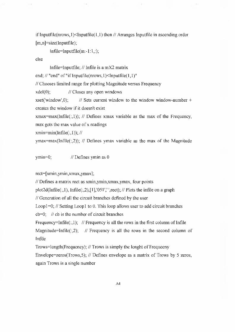
if Inputfile(nrows,l)<Inputfile(l,l) then // Arranges Inputfile in ascending order
[m,n]=size(Inputfile);
lnfde=Inp utfde(m: - 1 :1 ,:);
else
Infile=Inputfile; // Infde is a mX2 matrix
end; // "end" of "if Inputfile(nrows,l)<Inputfile(l,l)"
// Chooses limited range for plotting Magnitude versus Frequency
xdel(O); // Closes any open windows
xset('window',0); // Sets current window to the window window-number +
creates the window if it doesn't exist
xmax=max(Infile(:,l)); // Defines xmax variable as the max of the Frequency,
max gets the max value of x readings
xmin=min(Infile(:,l)); //
ymax=max(Infile(:,2)); // Defines ymax variable as the max of the Magnitude
ymin=0; // Defines ymin as 0
rect=[xmin,ymin,xmax,ymax];
// Defines a matrix rect as xmin,ymin,xmax,ymax, four points
plot2d(Infile(:,l), Infile(:,2),[l],'051',' ',rect); // Plots the infile on a graph
// Generation of all the circuit branches defined by the user
Loopl=0; // Setting Loopl to 0. This loop allows user to add circuit branches
cb=0 ; // cb is the number of circuit branches
Frequency=Infile(:,l); // Frequency is all the rows in the first column of Infile
Magnitude=Infile(:,2); // Frequency is all the rows in the second column of
Infile
Trows=length(Frequency); // Trows is simply the lenght of Frequecny
Envelope=zeros(Trows,5); // Defines envelope as a matrix of Trows by 5 zeros,
again Trows is a single number
A4
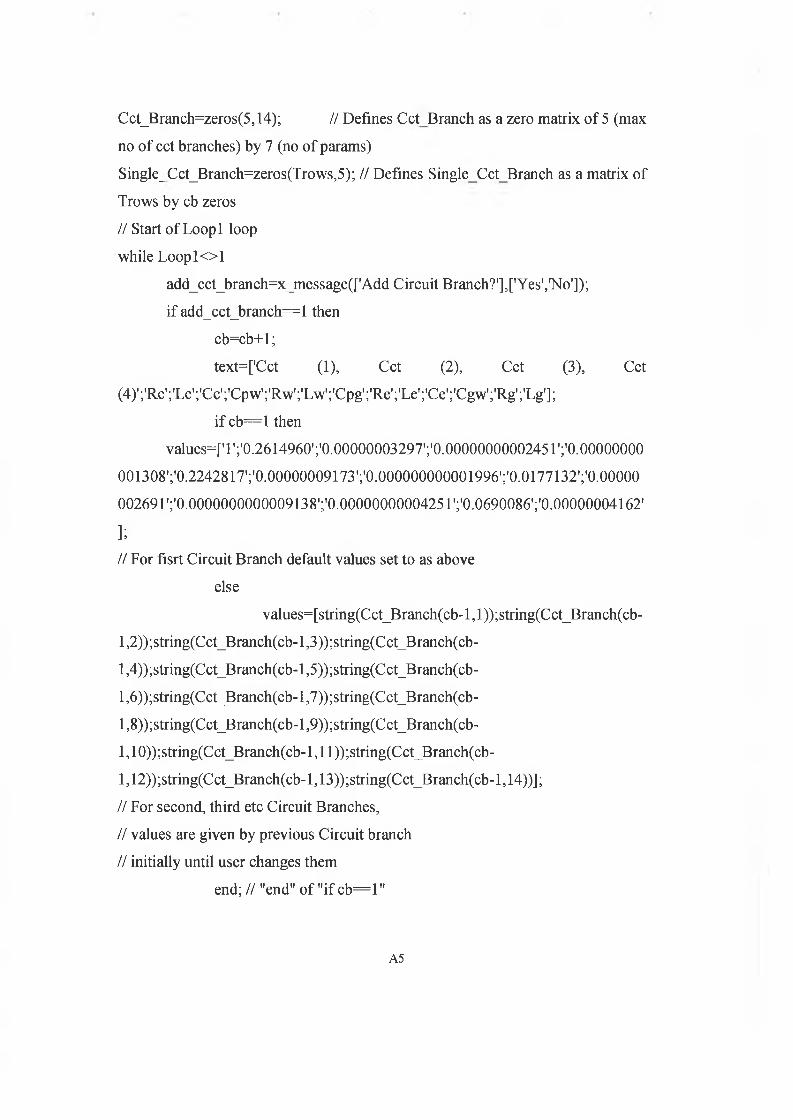
Cct_Branch=zeros(5,14); // Defines Cct Branch as a zero matrix of 5 (max
no of cct branches) by 7 (no of params)
Single_Cct_Branch=zeros(Trows,5); // Defines SingleCctBranch as a matrix of
Trows by cb zeros
// Start of Loop 1 loop
while L o o p lo l
add_cct_branch=x_message(['Add Circuit Branch?'],['Yes','No']);
if add_cct_branch==l then
cb=cb+l;
texH'Cct (1), Cct (2), Cct (3), Cct
(4)';'Rc';'Lc';'Cc';'Cpw';'Rw';'Lw';'Cpg';'Re';'Le';'Ce';'Cgw';'Rg';'Lg'];
if c b = l then
values=['l';'0.2614960';'0.00000003297';'0.00000000002451';'0.00000000
001308';'0.2242817';'0.00000009173';'0.000000000001996';'0.0177132';'0.00000
002691';'0.0000000000009138';'0.00000000004251';'0.0690086';'0.00000004162'
];// For fisrt Circuit Branch default values set to as above
else
values=[string(Cct_Branch(cb-l,l));string(Cct_Branch(cb-
1,2)); string(Cct_Branch(cb-1,3)); string(C ct_B ranch(cb -
l,4));string(Cct_Branch(cb-l,5));string(Cct_Branch(cb-
1,6));string(Cct_Branch(cb-l ,7));string(Cct_Branch(cb-
1,8));string(Cct_Branch(cb-l ,9));string(Cct_Branch(cb-
1,10));string(Cct_Branch(cb-1,1 l));string(Cct_Branch(cb-
1,12));string(Cct_Branch(cb-l, 13));string(Cct_Branch(cb-1,14))];
// For second, third etc Circuit Branches,
// values are given by previous Circuit branch
// initially until user changes them
end; // "end" of "if cb = l"
A5

props=x_mdialog('Enter Circuit Branch
Parameters',[text],[values]); // Interactive input function
Cct_Branch(cb,l)=eval(props(l)); // Circuit type selected inputted
// for props(l)
Cct_Branch(cb,2)=eval(props(2)); // Cpw of circuit branch cb
Cct_Branch(cb,3)=eval(props(3)); // Rgw of circuit branch cb
Cct_Branch(cb,4)=eval(props(4)); // Lgw of circuit branch cb
Cct_Branch(cb,5)=eval(props(5)); // Lgw of circuit branch cb
Cct_Branch(cb,6)=eval(props(6 )); // Lgw of circuit branch cb
Cct_Branch(cb,7)=eval(props(7)); // Lgw of circuit branch cb
Cct_Branch(cb,8)=eval(props(8)); // Lgw of circuit branch cb
Cct_Branch(cb,9)=eval(props(9)); // Lgw of circuit branch cb
Cct_Branch(cb,10)=eval(props(10)); // Lgw of circuit branch cb
Cct_Branch(cb,l l)=eval(props(l 1)); // Lgw of circuit branch cb
Cct_Branch(cb,12)=eval(props(12)); // Lgw of circuit branch cb
Cct_Branch(cb,13)=eval(props(13)); // Lgw of circuit branch cb
Cct_Branch(cb,14)=eval(props(14)); // Lgw of circuit branch cb
else
if cb= 0 then abort
end;
// This part gives you the option of putting the newer starting
// values for a given cicuit branch
number=[];
for n=l:cb
number(n)=string(n); // Converts a matrix into a matrix of
// strings
end; // "end" of "for n=l:cb"
number(cb+ 1 )='finished';
1 1 =list(",cb+1 ,number');
finished=0 ;
A6

while finished~=l then
numbranch=x_choices('Enter Circuit Branch number to
change',list(ll));
if numbranch == cb+ 1 then finished=l;
// This is if the user chooses Finished in the window
else
fmished=0 ;
text=['Cct (1), Cct (2), Cct (3), Cct
(^VRcVLcVCcVCpw'i'RwVLw^Cpg'i'ReVLeVCeVCgwVRgVLg'];values=[string(Cct_Branch(numbranch,l));string(Cct_Branch(numbranch,
2));string(Cct_Branch(numbranch,3));string(Cct_Branch(numbranch,4));string(C
ct_Branch(numbranch,5));string(Cct_Branch(numbranch,6));string(Cct_Branch(n
umbranch,7));string(Cct_Branch(numbranch,8));string(Cct_Branch(numbranch,9
));string(Cct_Branch(numbranch,10));string(Cct_Branch(numbranch,ll));string(
Cct_Branch(numbranch,12));string(Cct_Branch(numbranch,13));string(Cct_Bran
ch(numbranch, 14))];
props=x_mdialog('Enter Circuit Branch
parameters',[text],[values]);
Cct_Branch(numbranch,l)=eval(props(l));
Cct_Branch(numbranch,2)=eval(props(2));
Cct_Branch(numbranch,3)=eval(props(3));
Cct_Branch(numbranch,4)=eval(props(4));
Cct_Branch(numbranch,5)=eval(props(5));
Cct_Branch(numbranch,6)=eval(props(6));
Cct_Branch(numbranch,7)=eval(props(7));
Cct_Branch(numbranch,8)=eval(props(8));
Cct_Branch(numbranch,9)=eval(props(9));
Cct_Branch(numbranch, 10)=eval(props( 10)) ;
Cct_Branch(numbranch,l l)=eval(props(l 1));
Cct_Branch(numbranch, 12)=eval(props( 12)) ;
A7

Cct_Branch(numbranch, 13)=eval(props( 13));
Cct_Branch(numbranch,14)=eval(props(14));
end; // "end" of "if numbranch == eb+1 "
end; // "end" of "while finished~=l" loop
end; // "end" of "if add_cct_branch=l"
xdel(O); // Closes all windows
// This should be a 5 X 7 matrix with each circuit branch and the
// corresponding parameters
// This is a Trows X 5 zeros matrix at this point
//disp(Frequency); // This is a Trows X 1 column matrix
//disp(Magnitude); // This is a Trows X 1 column matrix
//disp(cb); // This is a single number giving the number of circuit
branches
//disp(Trows); // This is a single number giving the number of points in
Frequency
// Calculates Circuit Branch Magnitude versus Frequency
// and outputs it as Envelope
[Envelope]=pshapel(Cct_Branch,Envelope,Frequency,cb,Trows);
// Outputs Envelope in a new format
// Plots Cct_Branch
plotshape(Envelope,Frequency,Magnitude,cb); // Plots Magnitude and Envelope
// Peak fitting routine
Fitcircuit=x_message(['Do you want to run circuit fitting
routine?'],['Yes',"No']); // You click on yes or no, yes=l no=0
xdel(l);
xset('window',l);
xset('wdim',700,40);
xset('pattem',l);
A8
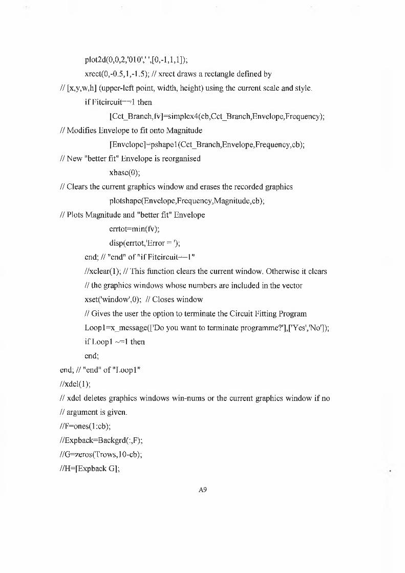
plot2 d(0 ,0 ,2 ,'0 1 0 ',' ',[0 ,-1 , 1 , 1 ]);
xrect(0,-0.5,l,-1.5); // xrect draws a rectangle defined by
// [x,y,w,h] (upper-left point, width, height) using the current scale and style,
if Fitcircuit==l then
[Cct_Branch,fv]=simplex4(cb,Cct_Branch,Envelope,Frequency);
// Modifies Envelope to fit onto Magnitude
[Envelope]=pshapel(Cct_Branch, Envelope, Frequency, cb);
// New "better fit" Envelope is reorganised
xbasc(O);
// Clears the current graphics window and erases the recorded graphics
plotshape(Envelope,Frequency,Magnitude,cb);
// Plots Magnitude and "better fit" Envelope
errtot=min(fv);
disp(errtot,'Error =');
end; // "end" of "if Fitcircuit==l"
//xclear(l); // This function clears the current window. Otherwise it clears
// the graphics windows whose numbers are included in the vector
xset('window',0); // Closes window
// Gives the user the option to terminate the Circuit Fitting Program
Loopl=x_message(['Do you want to terminate programme?'],['Yes',TSTo']);
if Loop 1 ~=T then
end;
end; // "end" of "Loopl"
//xdel(l);
// xdel deletes graphics windows win-nums or the current graphics window if no
// argument is given.
//F=ones(l:cb);
//Expback=B ackgrd(: ,F);
//G=zeros(Trows,10-cb);
//H=[Expback G];
A9

//Individs=Envelope+H;
// Gives the user the option to save the Params
if cb~ = 0 then
AllParams=[Frequency Magnitude];
saveParams=x_message(['Do you want to save Params?'],['Yes','No']);
if saveParams=l then
filename=xgetfile('*.dat','d:\scilab\raman\Params\7Enter a file
name');
errcatch(240," continue", "nomessage");
if filename ~ = " then
write(filename, AllParams,'( 13 (e 10.3))');
while iserror(240)=l
errclear(240);
text-File already exists: choose new name.';
filename=xgetfile('*.dat','E:\Program Files\Scilab-
2.7\Programs\Params\','Enter another file name');
if filename = " then
break
end; // "end" of "if filename =""
write(filename, AllParams,'( 13 (e 10.3))');
end; // "end" of "while iserror(240)=l"
end; // "end" of "if filename ~ = ""
end; // "end" of "if saveParams==l"
// Gives the user the option to see the Params in the Scilab window
display=x_message(['Do you want to see circuit branch Params';'(in
command window)?'],['Yes','No']);
for n=l:5
BranchData=Cct_Branch(n, 1);
if BranchData==0 then
A10

Area(n)=0;
else
A=0;
for m=2: Trows
A=A+(Frequency(m)-Frequency(m-
I )) * (Envelope(m,n)+Envelope(m-1 ,n))/2;
end; // "end" of "for m=2:Trows"
Area(n)=A;
end; // "end" of "if BranchData==0"
end; // "end" of "for n=l:5"
errtot=min(fv);
B ranchPar am s=[C ct_B r an ch Area];
if display=l then
disp('Branch Params = ',Branch_Params);
disp('Error = ',errtot);
end; // "end" of "if display==l"
end; // "end" "if cb~=0 "
plotshpape2
II Plots the Magnitude versus Frequency again and then plots each branch and
their Envelope versus Frequency
//
// copyright Brian Cregan
// 5/3/03
function []=plotshape(Envelope,Frequency,Magnitude,cb);
Sum=sum(Envelope,'c'); // Sum is a trows X 1 matrix
Xscale=[Frequency Frequency];
// Used to draw overall Magnitude and overall effect of cirtuit branches
Yscale=[Magnitude Sum];
// Used to draw overall Magnitude and overall effect of cirtuit branchesA l l

colours=[l 2 ];
for x=l:cb
Yscale=[Yscale Envelope(:,x)];
// Plot of Magnitude, Sum effect of all circuit branches, effect of each branch
Xscale=[Xscale Frequency];
// Simply the Frequency Sweep as the x-axis
colours=[colours x+2 ];
end;
Xl=Frequency(l);
// Defining points for window, XI is the first entry
// in the 1 column matrix Frequency
X2=Frequency(T rows);
// Defining points for window, X2 is the second entry in the
//1 column matrix Frequency
Y1=0; // Defining points for window, Y1 is 0
Ymag=max(Magnitude); // Defining points for window
Ysum=max(Sum); // Defining points for window
Y2=max(Ymag,Ysum); // Defining points for window,
// Y2 is the max Magnitude between Magnitude and Envelope
rect=[Xl,Yl,X2,Y2]; // Defining points for window
xset('window',0 );
xclear(O);
xbasc(O);
plot2d([Xscale], [Yscale], [colours] ,'051',' ',rect);
pshapel
II Calculates Frequency response of theoretical circuit
// copyright Brian Cregan
//
// 5/3/03A12

function [Envelope]=pshape 1 (Cct_Branch,Envelope,Frequency,cb,Trows);
for n=l :cb // cb is the number of circuit branches
BranchData=Cct_Branch(n,:);
// Sets BranchData as a variable that goes through the columns
// of each row of Cct_Branch matrix
select Cct_Branch(n,l)
// Uses column 1 of Cct_Branch, which represents the user's choice of circuit,
// to choose which case statement below will be used as a solver,
case 1 then // Magnitude of Plasma Circuit
Rc=BranchData(2);
Lc=BranchData(3);
Cc=BranchData(4);
Cpw=BranchData(5);
Rw=BranchData(6);
Lw=BranchData(7);
Cpg=BranchData(8);
Re=BranchData(9);
Le=BranchData( 10);
Ce=BranchData(l 1);
Cgw=BranchData( 12);
Rg=BranchData( 13);
Lg=BranchData( 14);
XLc=(2*%pi*Lc)* Frequency;
XCc=((2*%pi*Cc)*Frequency)A(-l);
XCpw=((2 * %pi * Cp w) * F requency)A(-1);
XLw=(2*%pi*Lw)*Frequency;
XCpg=((2 *%pi *Cpg) * F requency) A(-1);
XLe=(2*%pi*Le)*Frequency;
XCe=((2 *%pi *Ce) *Frequency)A(-1);
A13
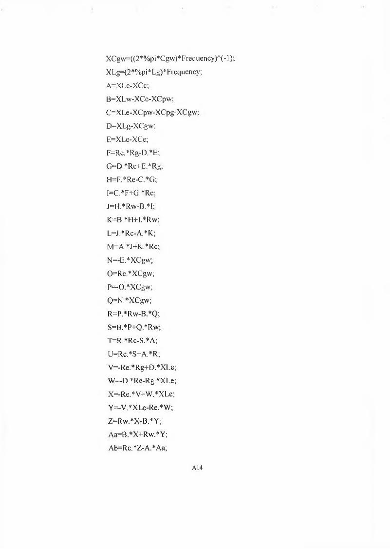
XCgw=((2*%pi*Cgw)*Frequency)A(-1 );
X Lg=(2 *%p i * Lg) * Freq ucncy ;
A=XLc-XCc;
B=XLw-XCc-XCpw;
C=XLe-XCpw-XCpg-XCgw;
D=XLg-XCgw;
E=XLe-XCe;
F=Re.*Rg-D.*E;
G=D.*Re+E.*Rg;
H=F.*Re-C.*G;
I=C.*F+G.*Re;
J=H.*Rw-B.*I;
K=B.*H+I.*Rw;
L=J.*Rc-A.*K;
M=A.*J+K.*Rc;
N=-E.*XCgw;
0=Re.*XCgw;
P=-0.*XCgw;
Q=N.*XCgw;
R=P.*Rw-B.*Q;
S=B.*P+Q.*Rw;
T=R.*Rc-S.*A;
U=Rc.*S+A.*R;
V=-Re.*Rg+D.*XLe;
W=-D.*Re-Rg.*XLe;
X=-Re.*V+W.*XLe;
Y=-V.*XLe-Re.*W;
Z=Rw.*X-B.*Y;
Aa=B.*X+Rw.*Y;
Ab=Rc.*Z-A.*Aa;
A 1 4
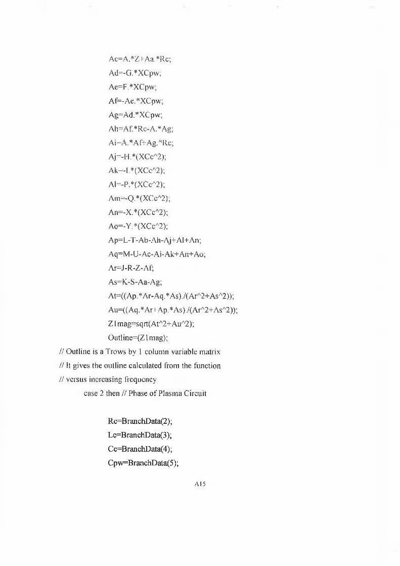
Ac=A.*Z+Aa.*Rc;
Ad=-G.*XCpw;
Ae=F.*XCpw;
Af=-Ae.*XCpw;
Ag=Ad.*XCpw;
Ah=Af. * Rc-A. * Ag;
Ai=A.*Af+Ag.*Rc;
Aj=-H.*(XCcA2);
Ak=-I.*(XCcA2);
AI=-P.*(XCcA2);
Am=-Q.*(XCcA2);
An=-X.*(XCcA2);
Ao=-Y.*(XCcA2);
Ap=L-T - Ab-Ah-Aj+Al+An;
Aq=M-U-Ac-Ai-Ak+An+Ao;
Ar=J-R-Z-Af;
As=K-S-Aa-Ag;
At=((Ap.*Ar-Aq.*As)./(ArA2+AsA2));
Au=((Aq.*Ar+Ap.*As)./(ArA2+AsA2));
Z1 mag=sqrt( AtA2+AuA2);
Outline=(Zlmag);
// Outline is a Trows by 1 column variable matrix
// It gives the outline calculated from the function
// versus increasing frequency
case 2 then // Phase of Plasma Circuit
Rc=BranchData(2);
Lc=BranchData(3);
Cc=BranchData(4);
Cpw=BranchData(5);
A I 5
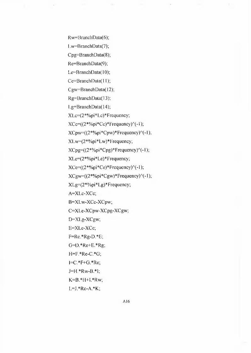
Rw=B ranch Data(6 );
Lw=BranchData(7);
Cpg=B ranch Data(8 );
Re=B ranch Data(9);
Le=BranchData( 10);
Ce=BranchData( 11);
Cgw=BranchData( 12);
Rg= B ran ch Data( 13);
Lg=BranchData(14);
XLc=(2*%pi*Lc)*Frequency;
XCc=((2*%pi*Cc)*Frequency)A(-l);
XCpw=((2*%pi*Cpw)*Frequeney)A(-1);
XLw=(2 *%p i * Lw)* Frequency;
XCpg=((2*%pi*Cpg)*Frequency)A(-1);
XLe=(2*%pi*Le)*Frequency;
XCe=((2 *%pi *Ce)* F requency)A(-1);
XCgw=((2*%pi*Cgw)* Frequency)A(-1);
XLg=(2*%pi*Lg)*Frequency;
A=XLc-XCc;
B^XLvv-XCc-XCpw;
C=XLe-XCpvv-XC’pg-XCgw;
D=XLg-XCgw;
E=XLe-XCe;
F=Re.*Rg-D.*E;
G=D.*Re+E.*Rg;
H=F.*Re-C.*G;
I=C.*F+G.*Re;
J=FI.*Rw-B.*I;
K=B.*H+l.*Rw;
L=J.*Rc-A.*K;
A 1 6
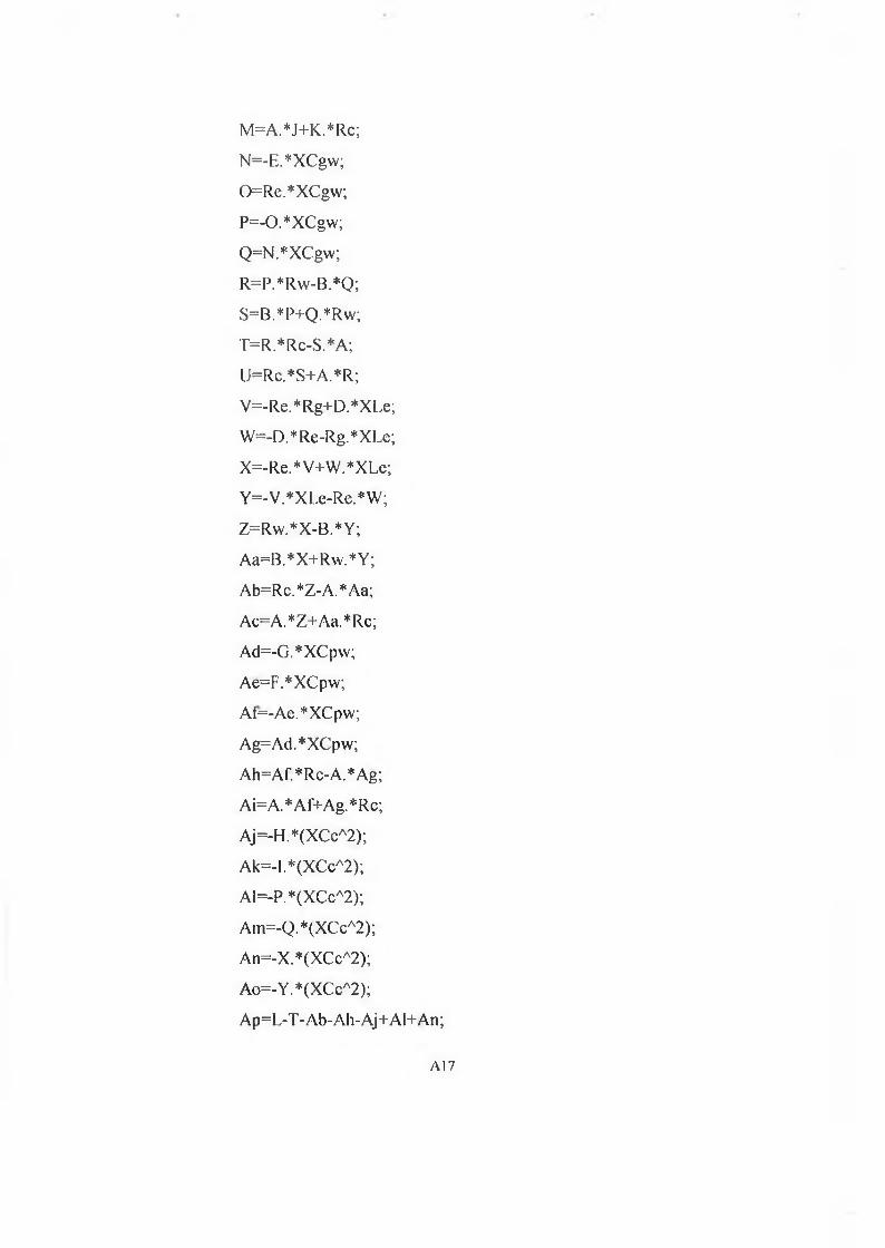
M=A.*J+K.*Rc;
N=-E.*XCgw;
0=Re.*XCgw;
P=-0.*XCgw;
Q=N.*XCgw;
R=P.*R\v-B.*Q;
S=B.*P+Q.*Rw;
T=R.*Rc-S.*A;
U=Rc.*S+A.*R;
V=-Re. * Rg+D. *XLe;
W=-D. * Re-Rg. *XLe;
X=-Re.*V+W.*XLe;
Y=-V.*XLe-Re.*W;
Z=Rvv.*X-B.*Y;
Aa=B.*X+Rw.*Y;
Ab=Rc.*Z-A.*Aa;
Ac=A.*Z+Aa.*Rc;
Ad=-G.*XCp\v;
Ae=F.*XCpw;
Af=-Ae.*XCpw;
Ag=Ad.*XC’pw;
Ah=Af.*Rc-A.*Ag;
Ai=A.*Af+Ag.*Rc;
Aj=-H.*(XCcA2);
Ak=-I.*(XCcA2);
Al=-P.*(XCcA2);
Am=-Q.*(XCcA2);
An=-X.*(XCcA2);
Ao=-Y.*(XCcA2);
Ap=L-T-Ab-Ah-Aj+Al+An;
A I 7

Aq=M-U-Ac-Ai-Ak+An+Ao ;
Ar=J-R-Z-Af;
As=K-S-Aa-Ag;
At=((Ap. *Ar-Aq. * As)./(ArA2+AsA2));
Au=((Aq. * Ar+Ap. * As)./(ArA2+AsA2));
Z 1 mag=atan(Au./At) ;
Outline=(Zlmag);
// Outline is a Trows by 1 column variable matrix
// It gives the outline calculated from the function
// versus increasing frequency
else
disp('Faulty Circuit (Outline Faulty');
abort;
end;
Envelope( : ,n)=Outl ine;
// Lists the outline for each cct branch (max of 5) in columns 1 to 5 of Envelope
end;
Simplex4
// Simplex fitting programme
//
// copyright Brian Cregan
// 5/3/03
function [Cct_Branch,fv]=simplex4(cb,Cct_Branch,Envelope,Frequency);
errclear(-l);
// All errors are cleared, for (n), n=+ it clears error no. n, for n=- clears all errors
[Params,CBtype]=columnl(Cct_Branch,cb);
// Params gives 1 column with parameter i/p for each circuit branch ADDED onlyA18

// CBtype gives type of circuit for each circuit branch in a 5 X 1 matrix
n=length(Params);
// Tells how many param values to be changed, as length of Params varies with
no. of branches added
maxcnt=1 2 0 *n;
// Counter max, limits number of iterations so that the program does not go on
indefinitely
tol=. 000001; // Tolerance set for acceptable fit of calculated curve
tol2=0.00001; // Tolerance set for acceptable fit of calculated curve
xin=Params; // This is done so that Params can be updated throughout the
program
v=Params(:); // v is a 30X1 (i.e. 1 column) matrix listing all the params of the
cct branches
cnt=0 ;
fv=Error2(Cct_Branch,Magnitude,Envelope,Frequency,cb,cnt,maxcnt);
// Function, fv is just one number
// It is the sum of the square of the differences
// between Mag and CB total at each freq point
// Also the time indicator window is drawn at this
// point as it is part of the o/p of Error2
for j= l :n // n is length of Params
delta=0.001; // Used to tell how much you vary a parameter
by, here variation is %50
zero_term_delta=0.25; // Just for when a paramamter value is zero
//disp(Params,'Params before y=');
y=Params(:);
// y is a 30X1 (i.e. 1 column) matrix listing all the params of the cct branches
if y(j)~=0 then // Individual point in Params
A19

y G )=( 1 +delta) *y (j); // Changes value of individual point
else
//y(j)=zero_term_delta;
// If a parameter is zero it is incremented to zero_term_delta
end;
v=[v y];
// A j+1 column matrix with y changing, v is the initial params. We end up with a
matrix
// that has the original parameters in the first column, then
// it has the the parameters
// in the next columns with each successive parameter changed by 50%
Params(:)=y; // Updated Params matrix
cnt=n;
[Cct_Branch]=update(Params,CBtype);
// Updates the Cct Branch matrix with the new Param matrix
// with 1 param changed by %50
f=Error2(Cct_Branch, Magnitude, Envelope, Frequency, cb,cnt,maxcnt);
// f is just 1 valued error signal and is
// calculated for the particular Cct_Branch
// with one parameter changed by %50
fv=[fv f);
// A matrix that gives the original error (fv) and then the error due to the change
// in 1 parameter (f)
end;
[fV,j]=sort(fv);
// fv is now a matrix that gives the intial error and the error by a change in a given
parameter of %50
// fv is a 1 X n+1 matrix that is in decreasing order
// fv is actual error in descending order, j is the index of each fv term
// This part finds the param that has the biggest effect on the error
A20

v=v(:j);// Picks out Params that gives smallest error, j equals n at this stage so we have a
n X n+1 matrix
// that gives the params of all 6 cct branches in each column, the first column is
// unchanged, and the
// next column has each consecutive parameter changed by 50%
// At the moment there are zeros for if the user inputs less than 6 cct branches
cnt=n+l;
alpha=l; beta=0.5;Gamma=2;
[n,npl]=size(v); // size function tells the dims of the matrix v, it will be nXn+1,
n= no. of rows, npl=> columns, i.e n+ 1
onesn=ones(l,n); // A 1 X n ones matrix
ot=2:n+l; // Simply a counter to run through 2 to n+1, for going through the
columns of v
on=l:n;
// Simply a counter to run through 1 to n, for going through the rows of v
// v is a 30X31 matrix.
// This takes the first column of v containing the user inputted
// paramters and generate
// a matrix that has the same values in all the columns as in the first column
while cnt<maxcnt
// maxcnt is 1 2 0 *n and limits number of iterations so that the program does not
// go on indefinitely
if max(max(abs(v(:,on)-v(:,onesn)))) <= tol & ... //
max(max(abs(fv(l)-fv(on)))) <= tol2 then
// This is the max of the absolute differences in error break
// before and after a change in the parameters
// if all the values are within the tolerance stop program
A21

// Inside the while cnt<maxcnt loop, the command break
// forces the end of the loop
end;
// Simplex algorithm starting
vbar=(sum(v(:,ot),'c')/n);
// Takes the average of all parameter 1, parameter 2 etc
// excluding the inputted parameters
// vbar is a 30X1 matrix
vr=(l+alpha)!t!vbar - alpha*v(:,l);
// vr is a 30X1 matrix with each index of vbar increased by 200% and
// the original inputted parameters subtracted
Params(:)=vr; // Updated Params matrix
[Cct_Branch]=update(Params,CBtype);
// This just puts the parameters and cct branch type back into 1 matrix
// i.e. Cct Branch for use later on in the program (see next line)
fr=Error2(Cct_Branch, Magnitude, Envelope, Frequency, cb,cnt,maxcnt);
// error is calculated with changed params
cnt=cnt+l;
vk=vr; // new matrix vk is defined as vr
fk=fr;
// new matrix fk is defined as fr, fr is error generated from adjusted params
if fr<fv(2 ) then
// if the error fr < the error due to a change in the first parameter
if fr<fv(n+l) then
// if the error fr < the error due to a change in
// all the parameters then new approach
ve=Gamma*vr + (1-Gamma)*vbar;
// ve= 4 times vr plus (minus 3 times vbar)
Params(:)=ve;
A22
[Cct_Branch]=update(Params,CBtype);
// This just puts the parameters and cct branch type
// back into 1 matrix i.e. Cct Branch for use later
// on in the program (see next line)
fe=Error2(Cct_Branch,Magnitude,Envelope,Frequency,cb,cnt,maxcnt);
// error is calculated with changed params
cnt=cnt+l;
if fe<fv(n+l) then
vk=ve;
fk=fe;
end;
end;
else
// if the error fr > the error due to a change in the first parameter
vt=v(:,n+l);
ft=fv(n+l);
if fr<ft then
vt=vr;
ft=fr;
end;
vc=beta*vt+ (l-beta)*vbar;
Params(:)=vc;
[Cct_Branch]=update(Params,CBtype);
fc=Error2(Cct_Branch,Magnitude,Envelope,Frequency,cb,cnt,maxcnt);
cnt=cnt+l
if fc<fv(2) then
vk=vc;
fk=fc;
else
for j=2:n
A23
v(:j)=(v(:,n+l)+v(:j))/2;
Params(:)=v(:j);
[Cct_Branch]=update(Params,CBtype);
fv(j)=Error2(Cct_Branch, Magnitude, Envelope, Frequency, cb,cnt,maxcnt);
end;
cnt=cnt+n-l;
vk=(v(:,2)+v(:,n+l))/2 ;
Params(:)=vk;
[Cct_Branch]=update(Params,CBtype);
fk=Error2(Cct_Branch,Magnitude,Envelope,Frequency,cb,cnt,maxcnt);
cnt=cnt+1 ;
end;
end;
v(:,l)=vk;
[fV,j]=sort(fv);
v=v(:j);
end; // "end" of "while cnt<maxcnt"
Params(:)=v(:,n+1);
if cnt==maxcnt then
disp('Warning: Maximum number of iterations exceeded');
end;
[Cct_Branch]=update(Params,CBtype);
Update
II Reconstructs Cet Branch from Params and CBtype that have been changed by
simplex4
// copyright Brian Cregan
//
// 5/3/03A24

function [Cct_BranchJ=update(Params,CBtype,cb);
for m=l :cb
// cb being the number of circuit branches added
Params=Params';
// Params is a 6 X 1 Matrix and is tranposed to give a I X 6 Matrix
Cct_Branch=[CBtype Params];
Params=Params';
end;
errcatch(5," continue")
if iserror(5)= I then
dispCcount = ',cnt)
abort
end;
A25