Embed Size (px)
Citation preview
Integrated Circuits in Communications
ikall, MOS-AK 07.05.04 slide 1
Modelling of Frequency Dispersion Effectsin
Hetero Field-Effect Transistors
Ingmar Kallfass*, H. Schumacher*, T.-J. Brazil***University of Ulm
**National University of Ireland, Dublin
Integrated Circuits in Communications
ikall, MOS-AK 07.05.04 slide 2
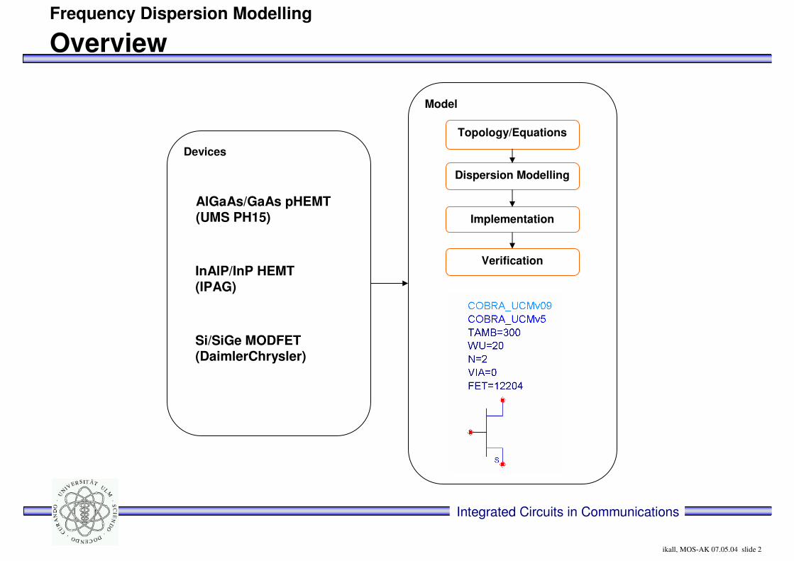
Devices
Model
Topology/Equations
Dispersion Modelling
Implementation
Overview
Verification
AlGaAs/GaAs pHEMT(UMS PH15)
Frequency Dispersion Modelling
InAlP/InP HEMT (IPAG)
Si/SiGe MODFET(DaimlerChrysler)
Integrated Circuits in Communications
ikall, MOS-AK 07.05.04 slide 3
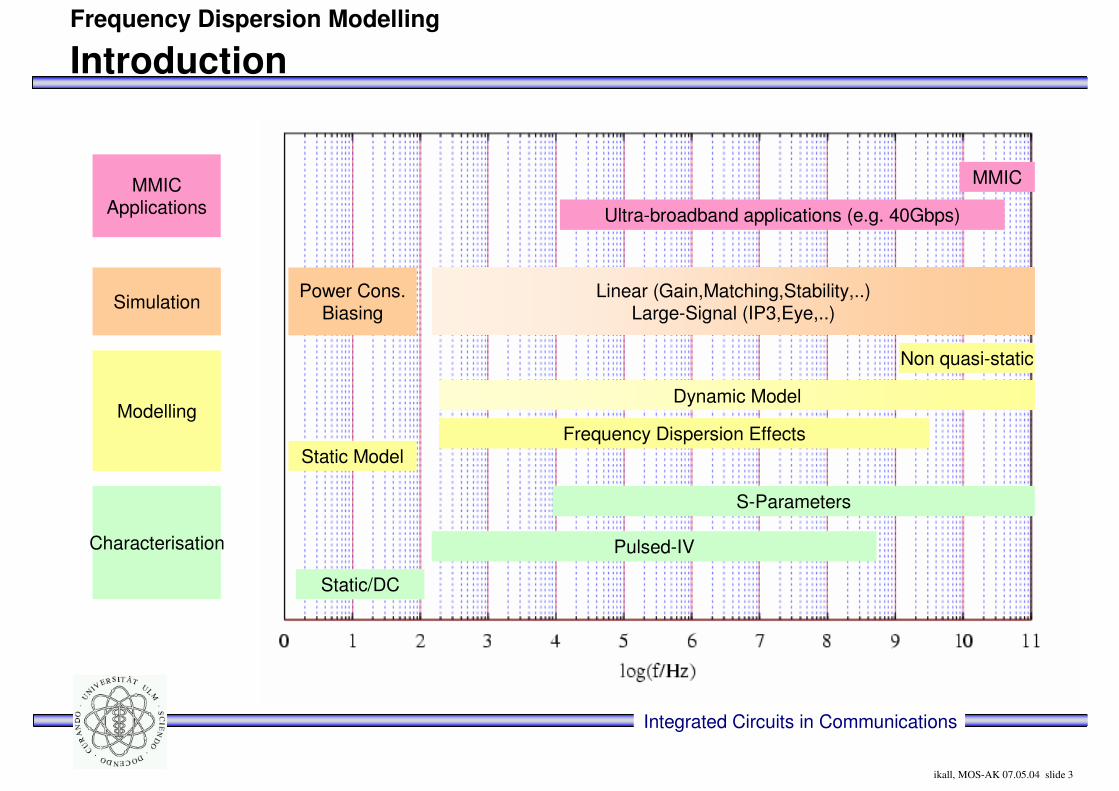
Introduction
Frequency Dispersion EffectsStatic Model
Dynamic Model
Non quasi-static
Power Cons.Biasing
Linear (Gain,Matching,Stability,..)Large-Signal (IP3,Eye,..)
Ultra-broadband applications (e.g. 40Gbps)
MMIC
Modelling
Simulation
MMICApplications
Characterisation
Static/DC
S-Parameters
Pulsed-IV
Frequency Dispersion Modelling
Integrated Circuits in Communications
ikall, MOS-AK 07.05.04 slide 4
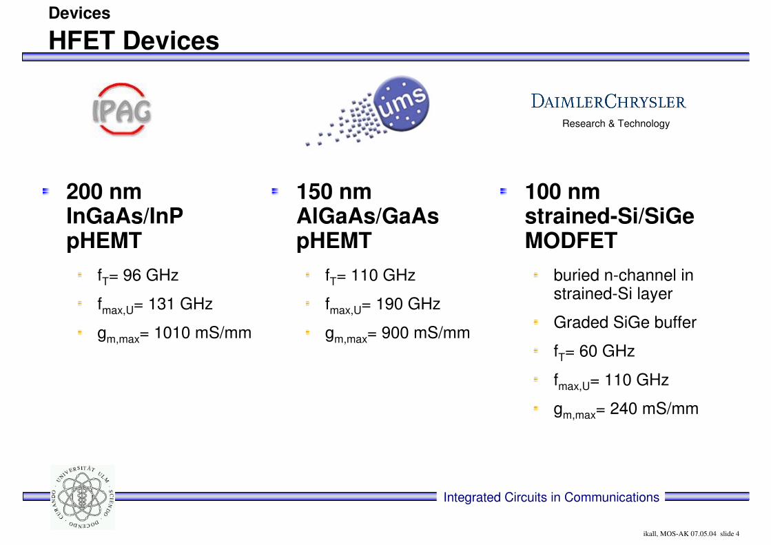
200 nm InGaAs/InPpHEMT
fT= 96 GHz
fmax,U= 131 GHz
gm,max= 1010 mS/mm
Devices
HFET Devices
150 nm AlGaAs/GaAspHEMT
fT= 110 GHz
fmax,U= 190 GHz
gm,max= 900 mS/mm
Research & Technology
100 nm strained-Si/SiGe MODFET
buried n-channel in strained-Si layer
Graded SiGe buffer
fT= 60 GHz
fmax,U= 110 GHz
gm,max= 240 mS/mm
Integrated Circuits in Communications
ikall, MOS-AK 07.05.04 slide 5
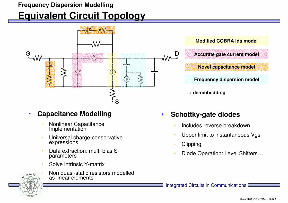
Equivalent Circuit Topology
Novel capacitance model
Accurate gate current model
Modified COBRA Ids model
Frequency dispersion model
Frequency Dispersion Modelling
+ de-embedding
Capacitance ModellingNonlinear Capacitance Implementation
Universal charge-conservative expressions
Data extraction: multi-bias S-parameters
Solve intrinsic Y-matrix
Non quasi-static resistors modelled as linear elements
Schottky-gate diodesIncludes reverse breakdown
Upper limit to instantaneous Vgs
Clipping
Diode Operation: Level Shifters…
Integrated Circuits in Communications
ikall, MOS-AK 07.05.04 slide 6
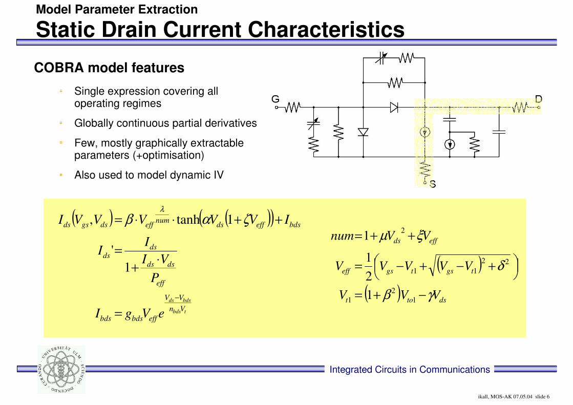
Static Drain Current CharacteristicsModel Parameter Extraction
COBRA model features
Single expression covering all operating regimes
Globally continuous partial derivatives
Few, mostly graphically extractable parameters (+optimisation)
Also used to model dynamic IV
( ) ( )( )
tbds
bdsds
VnVV
effbdsbds
eff
dsds
dsds
bdseffdsnumeffdsgsds
eVgI
PVI
II
IVVVVVI
−
=
⋅+=
++⋅⋅=
1'
1tanh, ζαβλ
( )( ) dstot
tgstgseff
effds
VVV
VVVVV
VVnum
γβ
δ
ξµ
−+=
����
�� +−+−=
++=
12
1
2211
2
121
1
Integrated Circuits in Communications
ikall, MOS-AK 07.05.04 slide 7
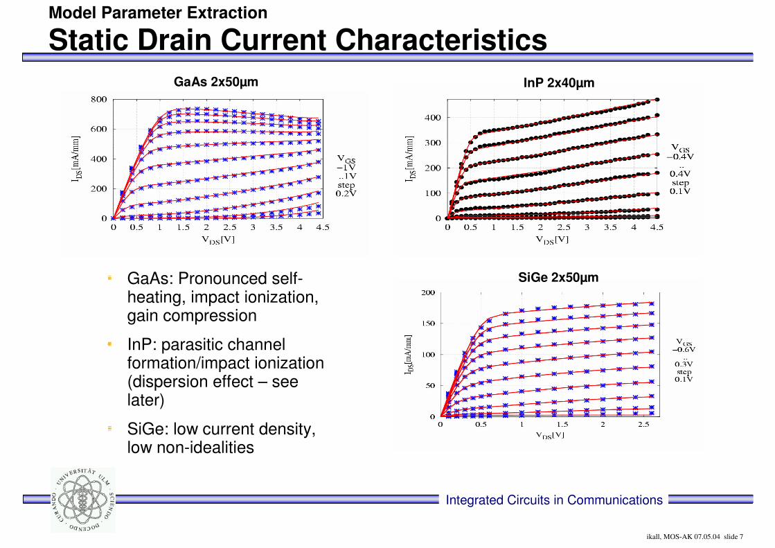
Static Drain Current CharacteristicsModel Parameter Extraction
GaAs: Pronounced self-heating, impact ionization, gain compression
InP: parasitic channel formation/impact ionization (dispersion effect – see later)
SiGe: low current density, low non-idealities
GaAs 2x50µm InP 2x40µm
SiGe 2x50µm
Integrated Circuits in Communications
ikall, MOS-AK 07.05.04 slide 8
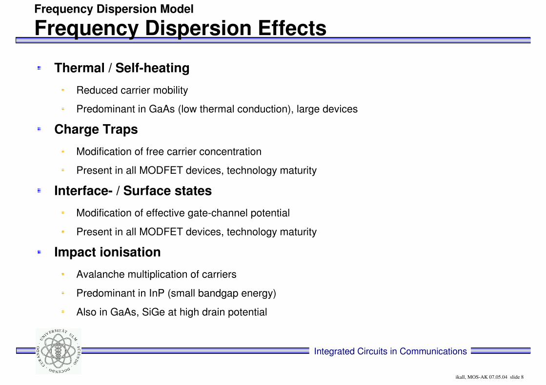
Frequency Dispersion EffectsFrequency Dispersion Model
Thermal / Self-heating
Reduced carrier mobility
Predominant in GaAs (low thermal conduction), large devices
Charge Traps
Modification of free carrier concentration
Present in all MODFET devices, technology maturity
Interface- / Surface states
Modification of effective gate-channel potential
Present in all MODFET devices, technology maturity
Impact ionisation
Avalanche multiplication of carriers
Predominant in InP (small bandgap energy)
Also in GaAs, SiGe at high drain potential
Integrated Circuits in Communications
ikall, MOS-AK 07.05.04 slide 9
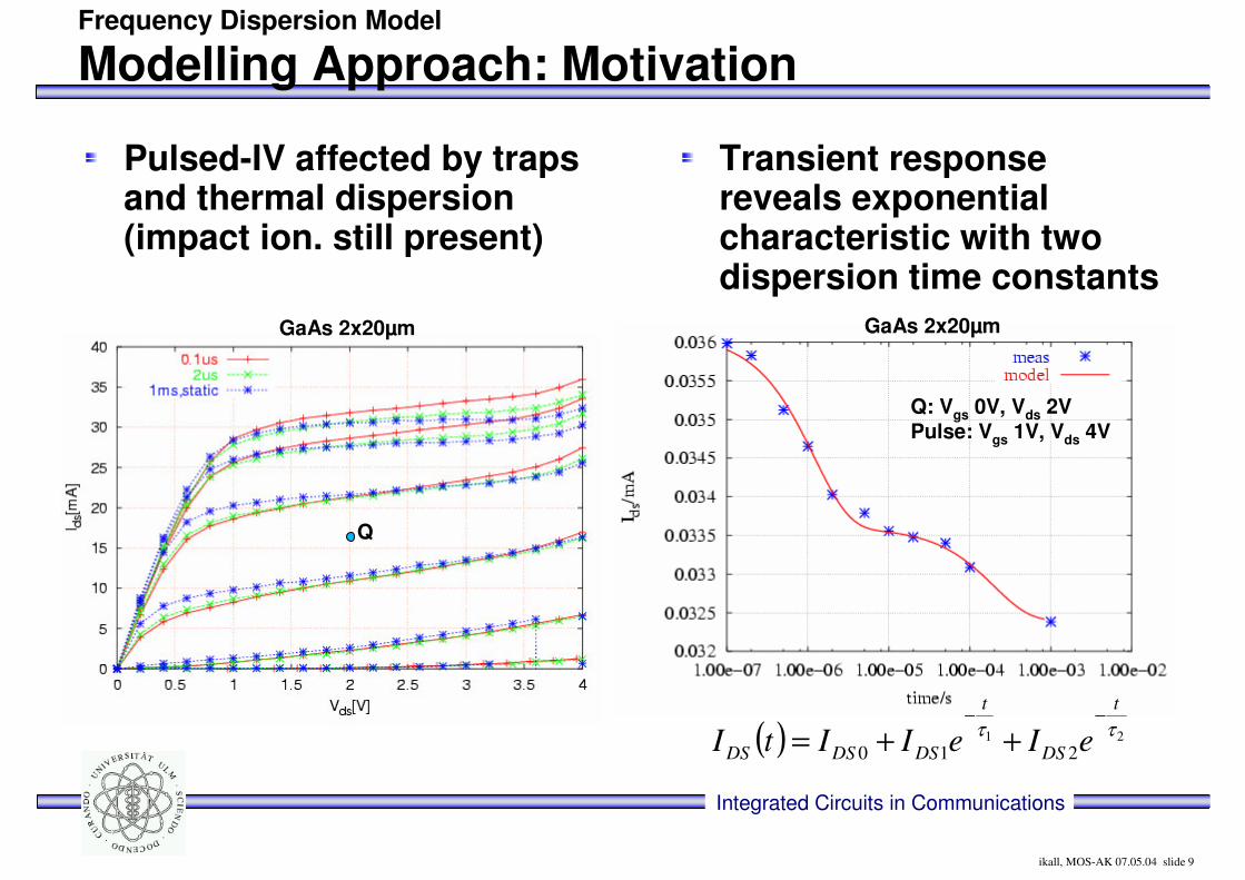
Transient response reveals exponential characteristic with two dispersion time constants
Modelling Approach: MotivationFrequency Dispersion Model
Pulsed-IV affected by traps and thermal dispersion (impact ion. still present)
( ) 21210
ττt
DS
t
DSDSDS eIeIItI−−
++=
Q
Q: Vgs 0V, Vds 2VPulse: Vgs 1V, Vds 4V
GaAs 2x20µm GaAs 2x20µm
Integrated Circuits in Communications
ikall, MOS-AK 07.05.04 slide 10
Dispersion Modelling: ApproachesFrequency Dispersion Model
Thermal modelsR-C thermal network models instantaneous channel temperature
Analytical basisCombine static&dynamic IV by empirical relationship deduced from measurements
Physical basisParameters (Vth, γ,..) function of frequency, temperature
Equivalent voltagesModify gate- and drain controlling voltages
Common drawbacks
Often no distinction between different dispersion effects
Frequency/Time transition usually not accuately modelled
May require additional iteration process during circuit analysis
Integrated Circuits in Communications
ikall, MOS-AK 07.05.04 slide 11
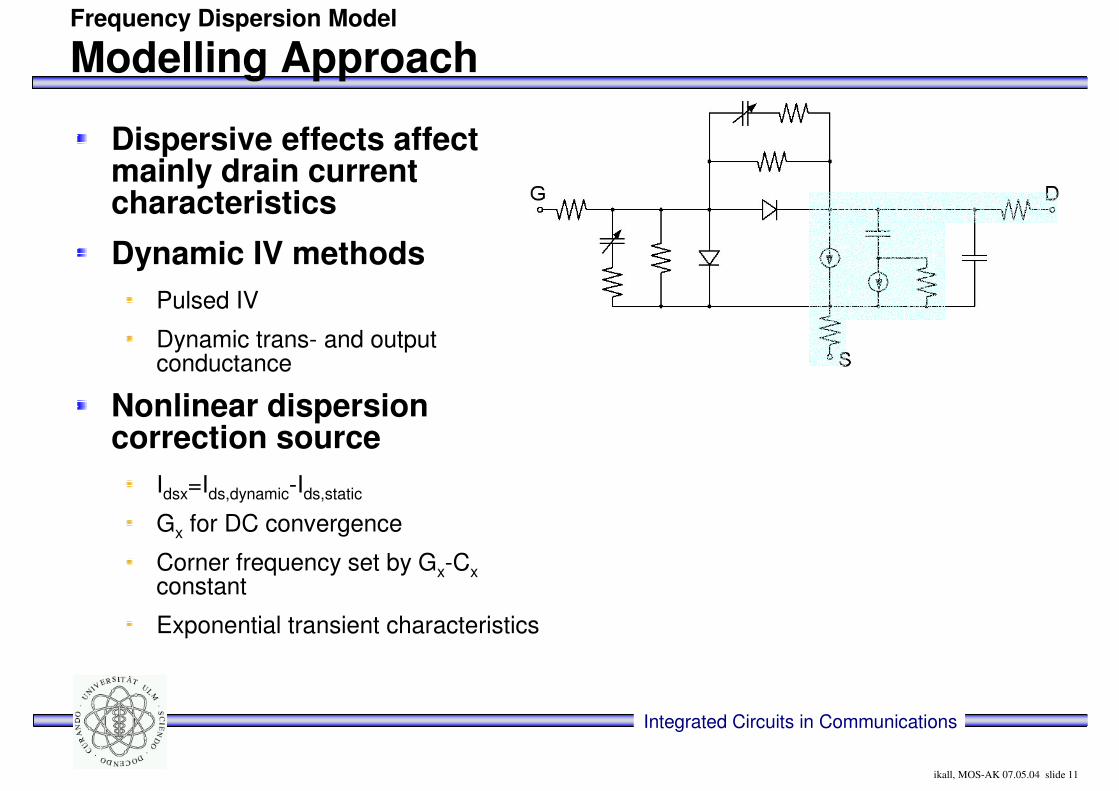
Modelling Approach Frequency Dispersion Model
Dispersive effects affect mainly drain current characteristics
Dynamic IV methodsPulsed IV
Dynamic trans- and output conductance
Nonlinear dispersion correction source
Idsx=Ids,dynamic-Ids,static
Gx for DC convergence
Corner frequency set by Gx-Cxconstant
Exponential transient characteristics
Integrated Circuits in Communications
ikall, MOS-AK 07.05.04 slide 12
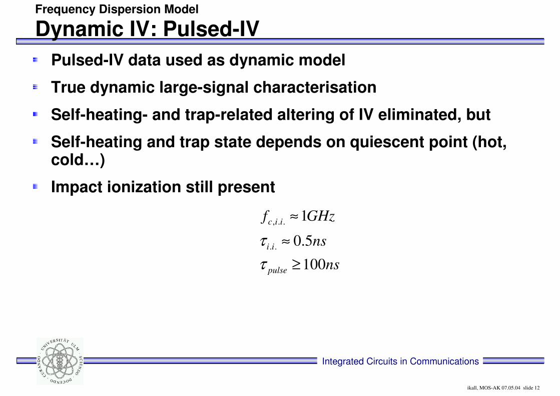
Dynamic IV: Pulsed-IVFrequency Dispersion Model
Pulsed-IV data used as dynamic model
True dynamic large-signal characterisation
Self-heating- and trap-related altering of IV eliminated, but
Self-heating and trap state depends on quiescent point (hot, cold…)
Impact ionization still present
ns
ns
GHzf
pulse
ii
iic
100
5.0
1
..
..,
≥≈
≈
ττ
Integrated Circuits in Communications
ikall, MOS-AK 07.05.04 slide 13
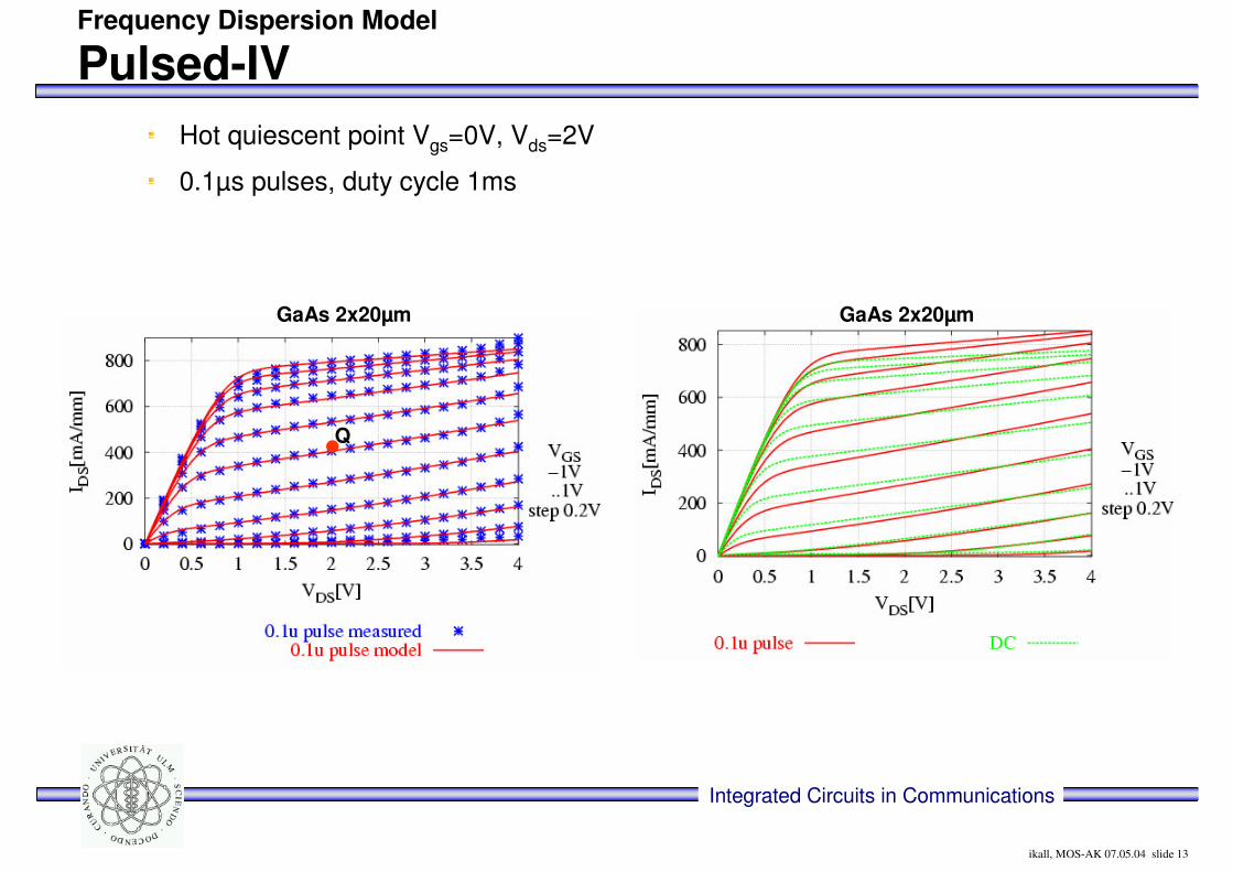
Pulsed-IVFrequency Dispersion Model
Hot quiescent point Vgs=0V, Vds=2V
0.1µs pulses, duty cycle 1ms
Q
GaAs 2x20µm GaAs 2x20µm
Integrated Circuits in Communications
ikall, MOS-AK 07.05.04 slide 14
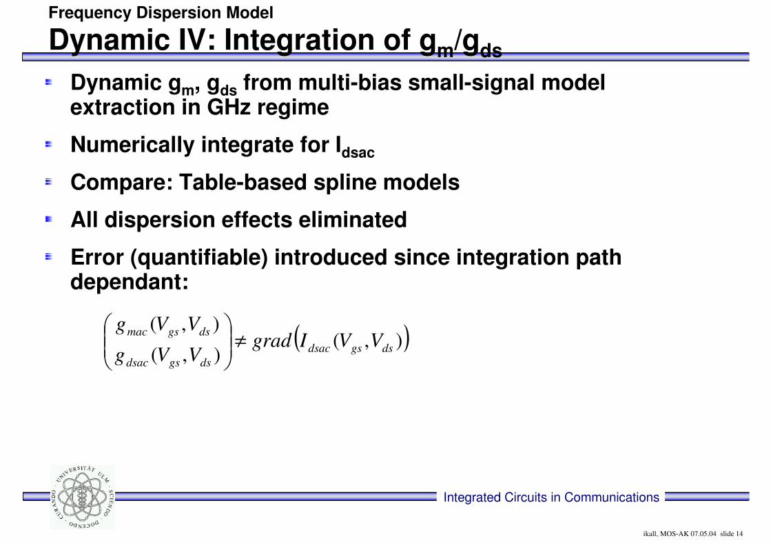
Dynamic IV: Integration of gm/gds
Frequency Dispersion Model
Dynamic gm, gds from multi-bias small-signal model extraction in GHz regime
Numerically integrate for Idsac
Compare: Table-based spline models
All dispersion effects eliminated
Error (quantifiable) introduced since integration path dependant:
( )),(),(),(
dsgsdsacdsgsdsac
dsgsmac VVIgradVVg
VVg≠��
�
����
�
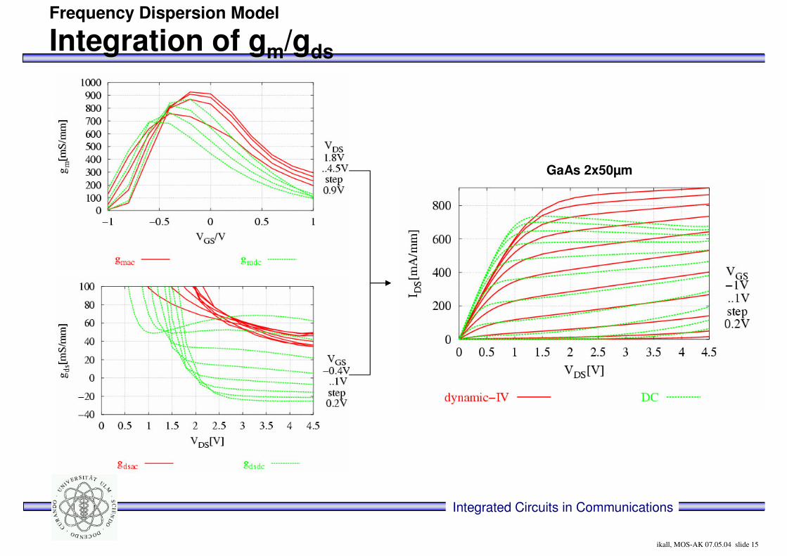
Integrated Circuits in Communications
ikall, MOS-AK 07.05.04 slide 15
Integration of gm/gds
Frequency Dispersion Model
GaAs 2x50µm
Integrated Circuits in Communications
ikall, MOS-AK 07.05.04 slide 16
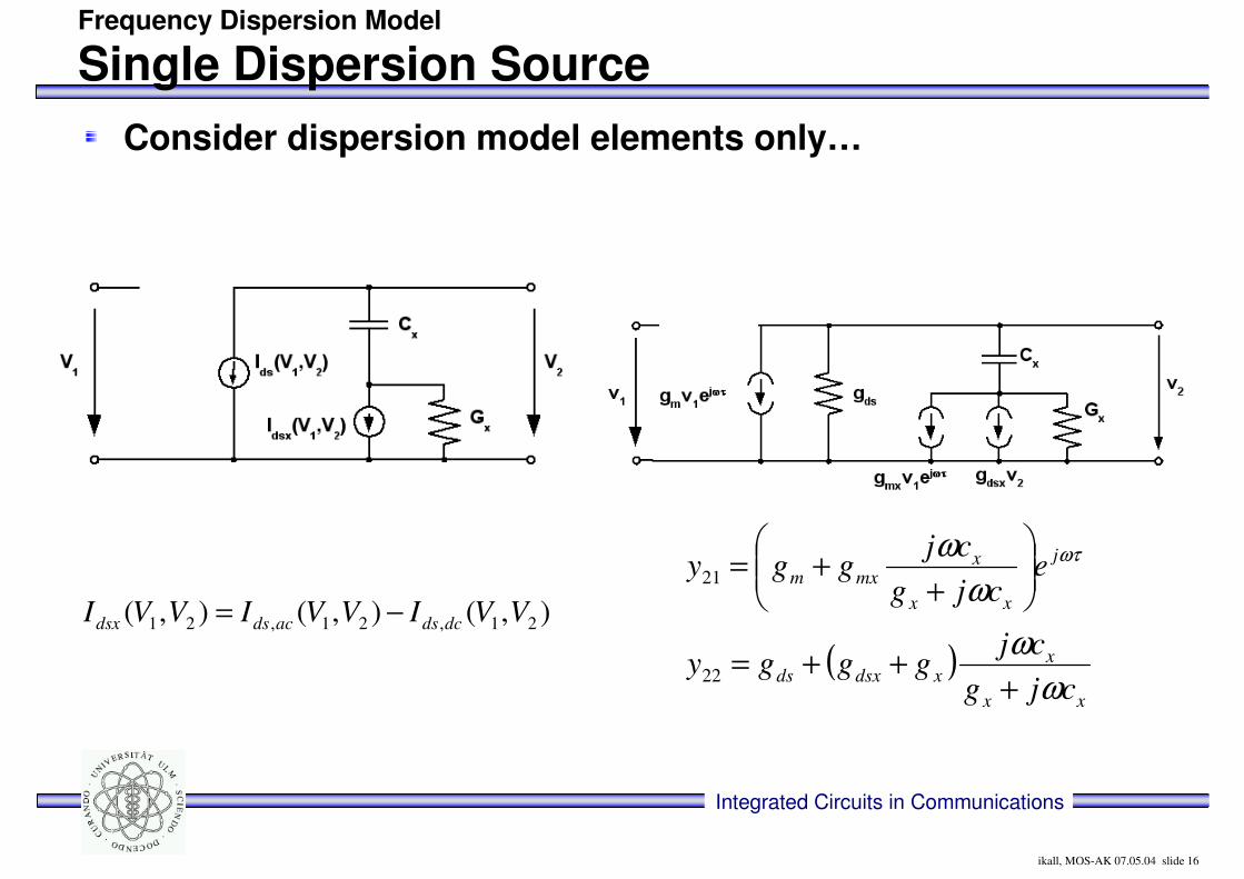
Single Dispersion SourceFrequency Dispersion Model
Consider dispersion model elements only…
),(),(),( 21,21,21 VVIVVIVVI dcdsacdsdsx −=
( )xx
xxdsxds
j
xx
xmxm
cjgcj
gggy
ecjg
cjggy
ωω
ωω ωτ
+++=
���
����
�
++=
22
21
Integrated Circuits in Communications
ikall, MOS-AK 07.05.04 slide 17
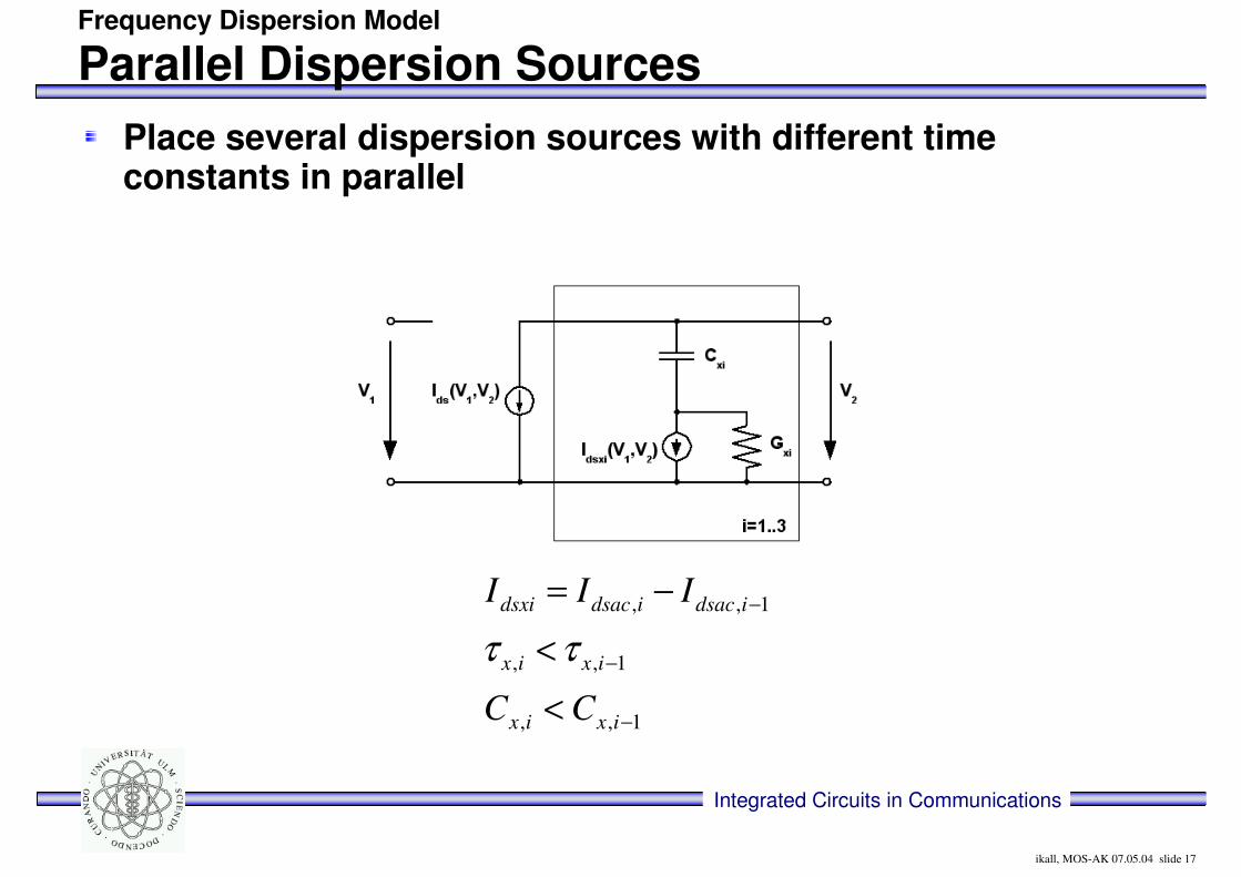
Parallel Dispersion SourcesFrequency Dispersion Model
Place several dispersion sources with different time constants in parallel
1,,
1,,
1,,
−
−
−
<<
−=
ixix
ixix
idsacidsacdsxi
CC
III
ττ
Integrated Circuits in Communications
ikall, MOS-AK 07.05.04 slide 18
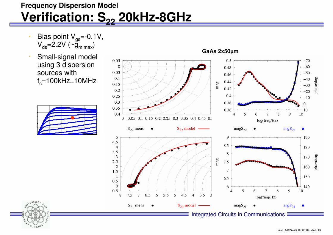
Verification: S22 20kHz-8GHzFrequency Dispersion Model
Bias point Vgs=-0.1V, Vds=2.2V (~gm,max)
Small-signal model using 3 dispersion sources with fc=100kHz..10MHz
GaAs 2x50µm
Integrated Circuits in Communications
ikall, MOS-AK 07.05.04 slide 19
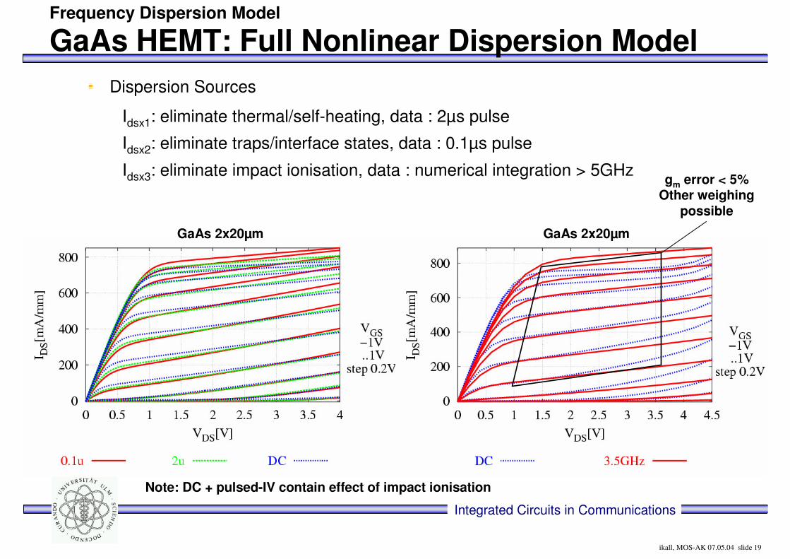
GaAs HEMT: Full Nonlinear Dispersion ModelFrequency Dispersion Model
Dispersion Sources
Idsx1: eliminate thermal/self-heating, data : 2µs pulse
Idsx2: eliminate traps/interface states, data : 0.1µs pulse
Idsx3: eliminate impact ionisation, data : numerical integration > 5GHz gm error < 5%Other weighing
possible
Note: DC + pulsed-IV contain effect of impact ionisation
GaAs 2x20µm GaAs 2x20µm
Integrated Circuits in Communications
ikall, MOS-AK 07.05.04 slide 20
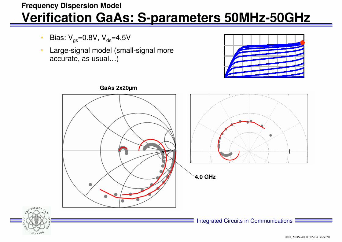
Verification GaAs: S-parameters 50MHz-50GHzFrequency Dispersion Model
Bias: Vgs=0.8V, Vds=4.5V
Large-signal model (small-signal more accurate, as usual…)
4.0 GHz
GaAs 2x20µm
Integrated Circuits in Communications
ikall, MOS-AK 07.05.04 slide 21
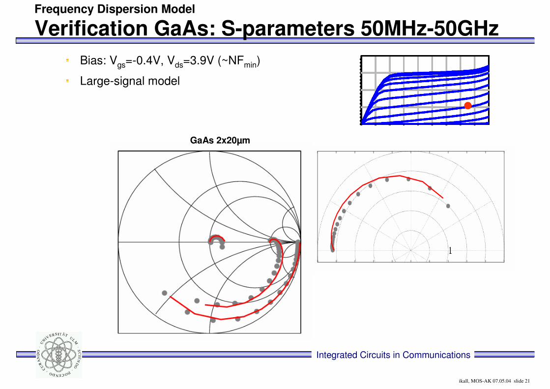
Verification GaAs: S-parameters 50MHz-50GHzFrequency Dispersion Model
Bias: Vgs=-0.4V, Vds=3.9V (~NFmin)
Large-signal model
GaAs 2x20µm
Integrated Circuits in Communications
ikall, MOS-AK 07.05.04 slide 22
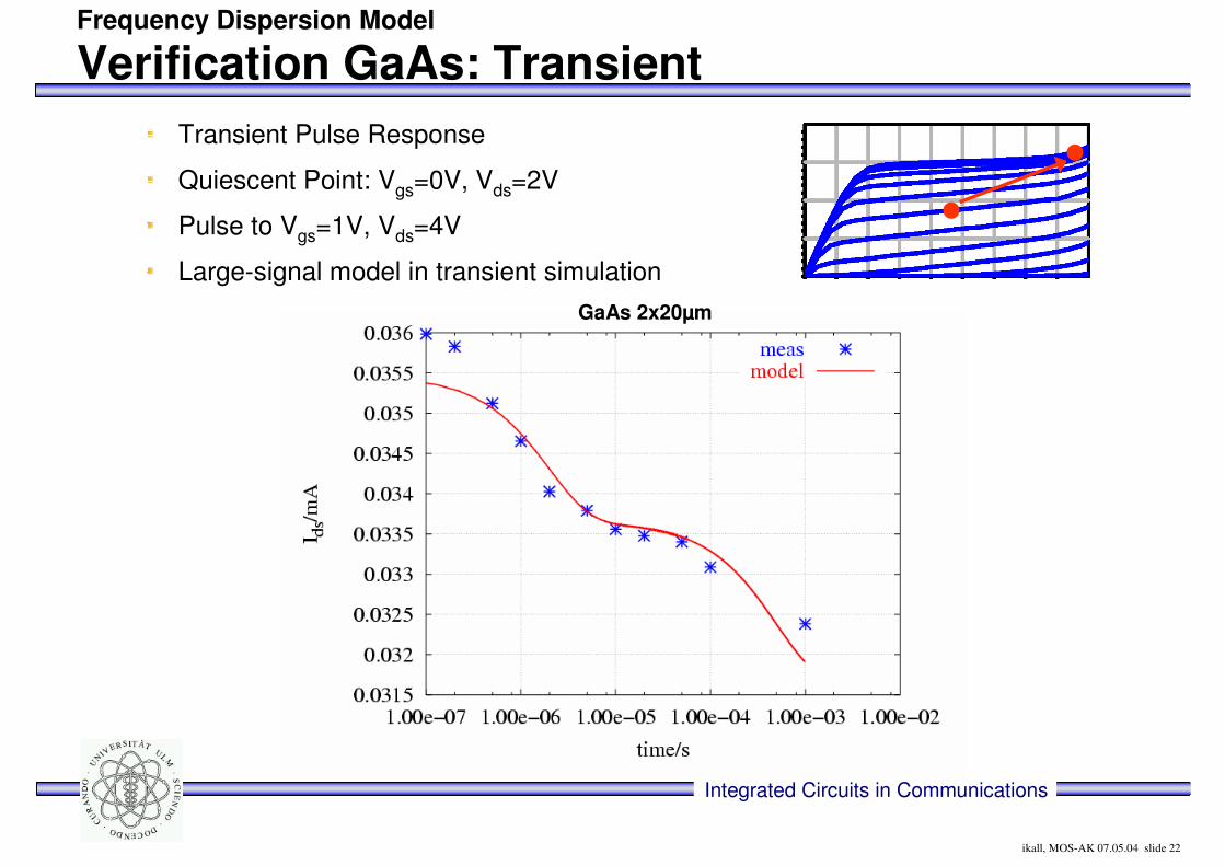
Verification GaAs: TransientFrequency Dispersion Model
Transient Pulse Response
Quiescent Point: Vgs=0V, Vds=2V
Pulse to Vgs=1V, Vds=4V
Large-signal model in transient simulationGaAs 2x20µm
Integrated Circuits in Communications
ikall, MOS-AK 07.05.04 slide 23
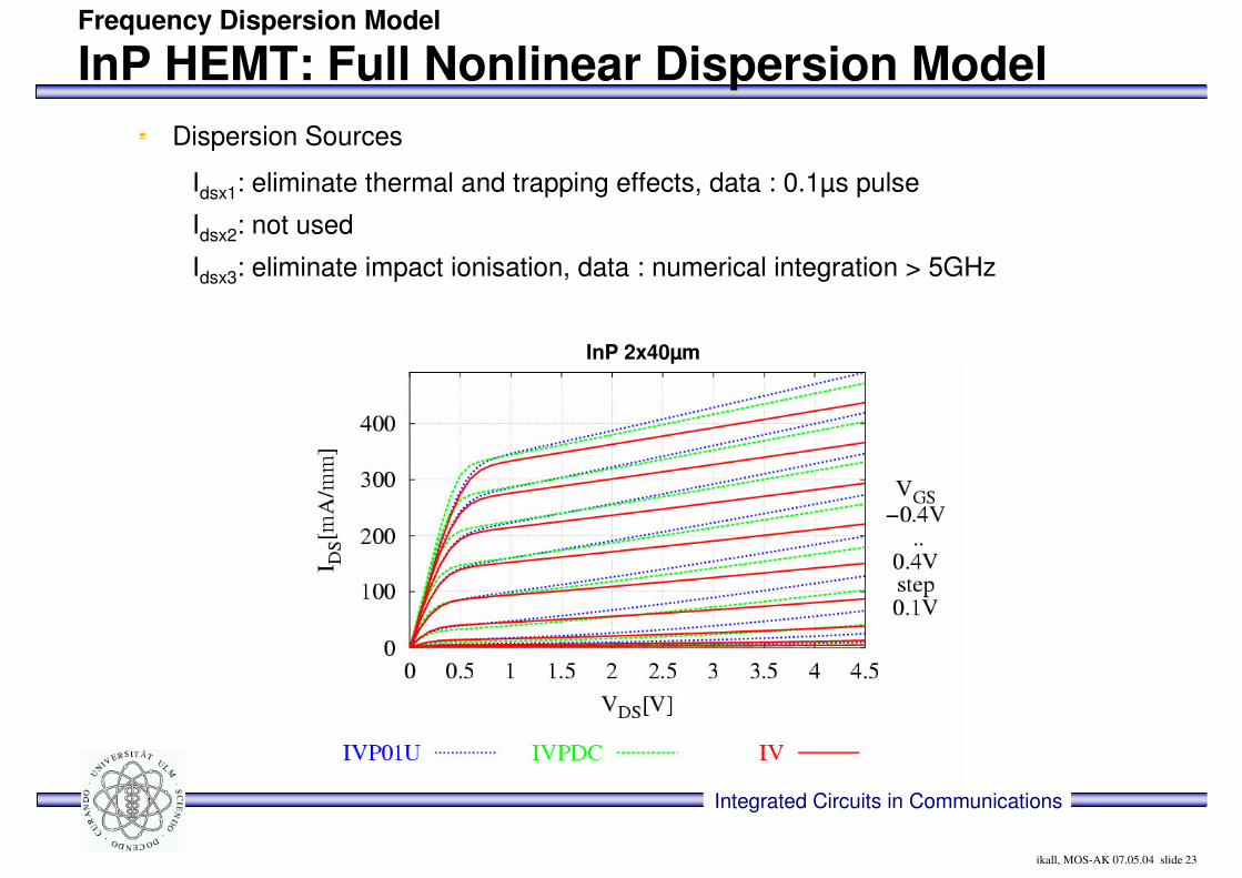
InP HEMT: Full Nonlinear Dispersion ModelFrequency Dispersion Model
Dispersion Sources
Idsx1: eliminate thermal and trapping effects, data : 0.1µs pulse
Idsx2: not used
Idsx3: eliminate impact ionisation, data : numerical integration > 5GHz
InP 2x40µm
Integrated Circuits in Communications
ikall, MOS-AK 07.05.04 slide 24
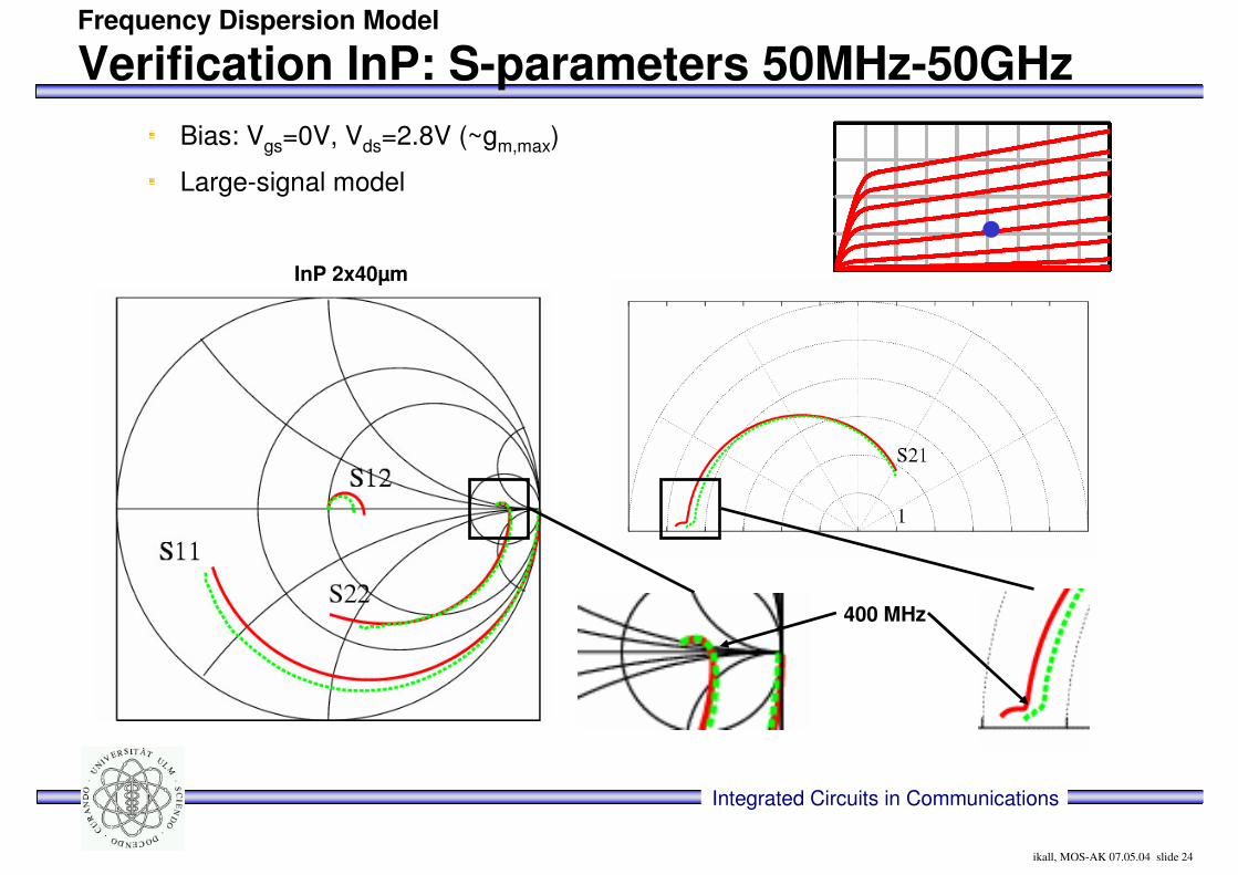
Verification InP: S-parameters 50MHz-50GHzFrequency Dispersion Model
Bias: Vgs=0V, Vds=2.8V (~gm,max)
Large-signal model
400 MHz
InP 2x40µm
Integrated Circuits in Communications
ikall, MOS-AK 07.05.04 slide 25
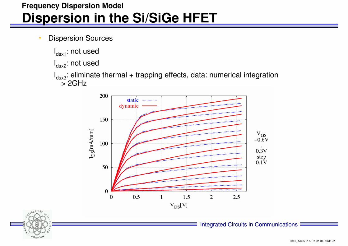
Dispersion in the Si/SiGe HFETFrequency Dispersion Model
Dispersion Sources
Idsx1: not used
Idsx2: not used
Idsx3: eliminate thermal + trapping effects, data: numerical integration > 2GHz
Integrated Circuits in Communications
ikall, MOS-AK 07.05.04 slide 26
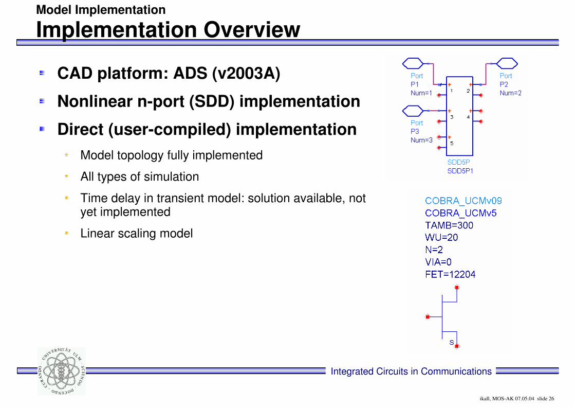
Implementation Overview
CAD platform: ADS (v2003A)
Nonlinear n-port (SDD) implementation
Direct (user-compiled) implementationModel topology fully implemented
All types of simulation
Time delay in transient model: solution available, not yet implemented
Linear scaling model
Model Implementation
Integrated Circuits in Communications
ikall, MOS-AK 07.05.04 slide 27
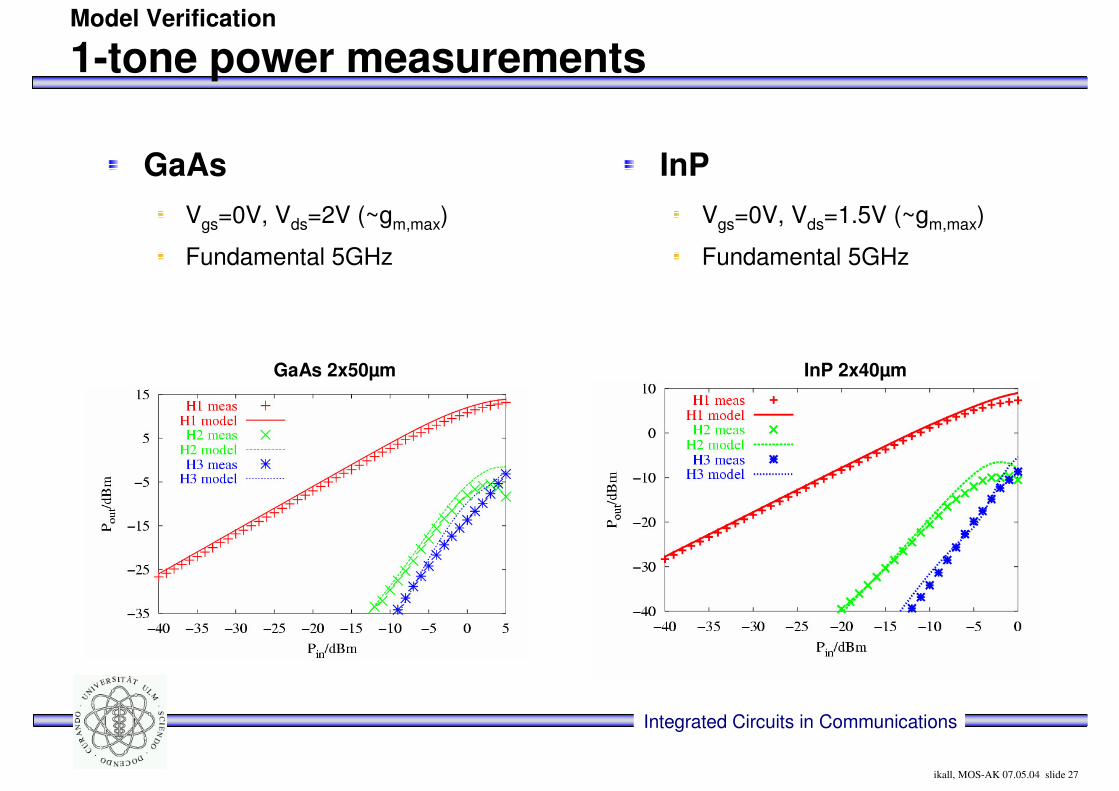
1-tone power measurementsModel Verification
GaAsVgs=0V, Vds=2V (~gm,max)
Fundamental 5GHz
InPVgs=0V, Vds=1.5V (~gm,max)
Fundamental 5GHz
InP 2x40µmGaAs 2x50µm
Integrated Circuits in Communications
ikall, MOS-AK 07.05.04 slide 28
Conclusion
Demonstration of nonlinear model incl. accurate frequency dispersion
Applicable to GaAs-, InP and strained-Si/SiGe HEMTs
Empirical: simulation efficiency, global validity, for circuit-design
User-compiled model implementation in ADS, suitable for all types of simulation
Dispersion model reflectsImpact of individual dispersion effects and their time constants/corner frequencies
Transition between dispersive regions in mag/phase
Dispersion model enablesUltra-broadband simulations (accurate PAE…)
Transient response simulations (e.g. pulsed power amps…)
Dispersion Modelling