Embed Size (px)
Citation preview

A 16X16 Basic-Cell High Speed Silicon Germanium Field
Programmable Gate Array
by
Peng Jin
A Thesis Submitted to the Graduate
Faculty of Rensselaer Polytechnic Institute
in Partial Fulfillment of the
Requirements for the degree of
Master of Science
Major Subject: Electrical Engineering
Advisor: _________________________________________ John F. McDonald, Thesis Advisor
Rensselaer Polytechnic Institute
Troy, New York November, 2007
(For Graduation December 2007)

I
CONTENTS
CONTENTS………………………………………………………........……………..I
LIST OF TABLES………………………………………………………........………III
LIST OF FIGURES………………………………………………………........……..IV
ACKNOWLEDGMENT……………………………………………………........…VII
ABSTRACT V………………………………………………………........………….III
1. Introduction………………………….……………………………........…………1
1.1 Research History………………………………………………........….….1
1.2 Thesis Outline……………………………………………………………..3
2. FPGA and XC6200 Architecture…………………………………………………4
2.1 FPGA……………………………………………………………………...4
2.2 Xilinx 6200 Field Programmable Logic Array……………………………6
3 Silicon Germanium (SiGe) Proces…………………………………………………13
3.1 SiGe HBT Process Overview………………………………………….…13
3.2 Performance Advantage………………………………………………….15
3.3 Graded Base HBT……………………………………………………..…15
3.4 IBM SiGe Proces…………………………………………………………16
3.5 Current Mode Logic (CML) ……………………………………………..19
3.6 Difficulties of designing a CML high speed FPGA………………..….…24
4 Large Scale (16 x16 BC array) SiGe FPGA design…………………………...…25
4.1 The XC 6200 Basic Cell…………………………………………….……25
4.2 Voltage Controlled Oscillator (VCO) in SiGe FPGA……………..……..32
4.3 Input multiplexer block, output selection blocks and FPGA core….……34
4.4 Programming scheme in the Basic Cell and FPG……………………..…34
4.5 Power Rails design …………………………………………………….…38
4.6 Clock and programming circuit clock distributions…………………...…41
4.7 SiGe FPGA Basic Cell Configuration……………………………………45
4.8 Programming the Basic cell array……………………………………..…50
4.9 Pin assignments of the 16 x 16 FPGA……………………………………52

II
4.10 layout, programming sequence and power consumption…………….…53
5 the 16 x 16 SiGe FPGA Test and a New Chip Design……………………………56
5.1 the 16 x 16 FPGA chip test…………………………..………………..…56
5.2 16 x 16 SiGe FPGA Test Results…………………………………………61
5.3 the New 16 x 16 FPGA chip design………………………………………65
5.4 Future work……………………………………………………………….65
REFERENCE………………………………………………………………………..67

III
LIST OF TABLES
Table 2.1 XC6200 family……………………………………………………………...7
Table 2.2 Function Derivation Table of the BCI……………………………………..12
Table 3.1 HBT comparison for 0.5 μm, 0.25 μm, and 0.18 μm generations…………13
Table 3.2 Equations of the CML buffer………………………………………………21
Table 3.3 Performance of the SiGe CML……………………………………………22
Table 4.1 Dynamic Routing Power Usage. ………………………………………..31
Table 4.2 Characteristics of the metal layers of the IBM 7 HP process…………...…39
Table 4.3 Equations for calculating power droop and power rail width……………..39
Table 4.4 Control signals of the input MU………………………………………...…46
Table 4.5 Configuration of the input MUX: X1, X2 and X3. …………………….…47
Table 4.6 Selection of the combinational and sequential operation ………………….47
Table 4.7 Selection of the CLB combinational or sequential outputs. ………………48
Table 4.8 Configuration of the MUX of Output Routing Stage. …………………….48
Table 4.9 Bit pattern of the Basic Cell………………………………………….……49
Table 4.10 Estimated power consumption of the different Basic Cell configurations
………………………………………………………………………………...…55

IV
LIST OF FIGURES
Figure 2.1 Structure of an FPGA…………………………..……………………..........6
Figure 2.2 XC6200 FPGA accelerates DSP application block………….……………..7
Figure 2.3 Schematic of the XC6200 Basic Cell ……………………………………...8
Figure 2.4 Schematic of the Function Unit in the XC6200 Basic Cell……………..…9
Figure 2.5 Connections between neighboring Basic Cells……………..…………...…9
Figure 2.6 4x4 cell block and Length 4 FastLANEs.…………………………...……10
Figure 2.7 Connections between 4x4 blocks (16x16 block).…………………...……11
Figure 2.8 Function Unit of XC6200…………………………………...……………11
Fig. 3.1 IBM foundry SiGe BiCMOS technology roadmap…………………………14
Figure 3.2 Energy band diagram for Si BJT and graded-base SiGe both biased in
forward active mode at low injection. ………………………………………………15
Figure 3.3 Ge content design trade-off …………………………………………..…16
Figure 3.4 Cutoff frequencies of several SiGe Technologies…………………..……17
Figure 3.5 Tf vs. CI curve for IBM SiGe 7HP technolog……………………… 17
Figure 3.6 Max. Switching frequency versus power consumption of CML and ECL
logic……………………………………………………………………………...20
Figure 3.7 A conventional CML Buffer………..…………………………………….21
Figure 3.8 Transfer characteristics of the CML buffer at different values of β..…….22
Figure 3.9 CML D-latch configuration with two input levels. ………………………23
Figure 3.10 Propagation delay of the CML buffer with the emitter size of 0.2 x 0.64
µm.……………………………………………………………………..…..…….23
Figure 4.1 Block diagram of the 16 x 16 array FPGA……………………………….25
Figure 4.2 XC6200 Basic Cell …………………………………………………….…26
Figure 4.3 Redesigned input routing block. …………………………………………27
Figure 4.4 General form of the new MUX design. The new input routing stage has 4:1
and 5:1 MUXs and the new output routing stage has 4:1 MUXs……………..…27
Figure 4.5 Latch 1 in the new D-FF design……………………………………….…28

V
Figure 4.6 Latch 2 in the new D-FF design……………………………………….…29
Figure 4.7 Schematic of the BCII. ………………………………………………..…29
Figure 4.8 Layout of the Basic Cell…………………………………………………30
Figure 4.9 Layout of the new Basic Cell……………………………………………31
Figure 4.10 the VCO’s architecture. ……………………………………………..…32
Figure 4.11 Schematic of the VCO buffer………………………………………..…33
Figure 4.12 Layout of the VCO buffer Figure 4.12 Layout of the VCO buffer. ……33
Figure 4.13 Block diagram of the input/output blocks and the FPGA core. ……..…33
Figure 4.14 Schematic of the programming scheme with clock distribution. ………35
Figure 4.15 Layout of 42 SRAM cells. ……………………………………………..35
Figure 4.16 Layout of 42 bits shift register…………………………………….……35
Figure 4.17 Simulation of the 42-bit memory…………………………………….....36
Figure 4.18 Simulation result of the shift register output with input data period of 800
ps………………………………………………………………………….…36
Figure 4.19 Block diagram of an array of basic cells with programming circuits
connected. ………………………………………………………………………..…37
Figure 4.20 Programming and memory circuits in the SiGe FPGA. …………….…37
Figure 4.22 Simplified circuit model of the power distribution. ……………………38
Figure 4.23 (a) Vcc (GND) power rail in the Basic Cell.. (b) Vee (-2.8 V) power rail
of the Basic Cell. ……………………………………………………………………40
Figure 4.24 Clock tree of the 8x8 array as an example in the FPGA core. …………40
Figure 4.25 Schematic (a) and layout (b) of the clock repeater…………………..…41
Figure 4.26 Test structure of the repeater driving capability. ………………………42
Figure 4.27 Simulation result of the clock repeater driving 400~700µm wire loads
with the 10 GHz test signal. ………………………………………………………..42
Figure 4.28 Simulation result of the clock repeater loaded with one to five clock
repeater loads. …………………………………………………………………42
Figure 4.29 Propagation delay between A, B, C and D in clock tree shown in Figure
4.30. …………..………………………………………………………………..43
Figure 4.30 Clock distribution of the SiGe FPGA…………..………………………43
VI
Figure 4.31 Detail clock distribution circuit in the 4 x 4 BC array. ………………..44
Figure 4.32 Schematic of the BCII. ………………………………………………..45
Figure 4.33 Schematic of the MUXs in the input routing stage of a BC. …………46
Figure 4.34 Configuration of the MUX bused in the Output Routing Stage. ……..48
Figure 4.35 Configuration data path in the 4x4 BC array. …………………………51
Figure 4.36 Block diagram and data stream path of the 8 x 8 BC array. ……….…51
Figure 4.37 Programming Circuit. …………………………………………………52
Figure 4.38 Pin arrangement of the 16-pin probe used in the 16 x 16 SiGe FPGA...53
Figure 4.39 Pin arrangement of the 10-pin power probe used in the 16 x 16
FPGA.…………………………………………………………………………53
Figure 4.40 16 x 16 FPGA array programming structure. …………………………54
Figure 4.41 Timing diagram of the SiGe FPGA. …………………………………...54
Figure 5.1 Pseudorandom binary sequences. ………………………………………56
Figure 5.2 Schematic of a four bit linear feedback sequences register (LFSR). …...56
Figure 5.3 Test circuitry of the 16 x 16 SiGe FPGAHigh speed input and output
signals…………………………………………………………………………57
Figure 5.4 Pin assignment of the high speed (> 10 GHz) signals. ………………...58
Figure 5.5 Input / Output arrangement of the programming data. …………………59
Figure 5.6 Schematic of the tapered buffer driving a 180 μm wire. ……………….59
Figure 5.7 Pin assignment of the low speed (> 1 GHz) inputs and outputs………...60
Figure 5.9 Test blocks on programming the SiGe FPGA configuration with an FPGA
board…………………………………………………………………………..61
Figure 5.10 8-stage Ring Oscillator Test Circuitry…………………………………62
Figure 5.11 8-stage Ring Oscillator Test Result……………………………………62
Figure 5.12 2-stage Ring Oscillator Test circuitry. ………………………………...63
Figure 5.13 2-stage Ring Oscillator Test Result……………………………………64

VII
ACKNOWLEDGMENT
I would like to thank my advisor Professor John F. McDonald for his great
support and advice through out my Master program at Rensselaer. Prof. McDonald
gave me the opportunity to be working with the latest technologies on this SiGe
FPGA project together with some great ideas and suggestions on both the project
and my study life at RPI. He is kind to all his students and keeps working every
day for our current projects and group’s future. I really appreciate what he did for
us.
I would like to thank Professor Russell P. Kraft and Steve Nicolas for the
great help on the whole process of my chip test.
My group members always support me by kinds of methods. Dr. Jong-ru Guo
designed the first working FPGA chip, and was still concerned about the project
even after he graduated. Michael Chu, and Dr. Okan Erdogan did a great help on
my design and test. Dr. Young Yim and Jimwoo Kim are always there when I
need their help. Philip Jacob and Aamir Zia are two good friends to talk with on
any technical questions.
Finally I would like to thank my Family and friends for keeping motivated
while I pursued a long academic program.

VIII
ABSTRACT The Field Programmable Gate Array (FPGA) is a configurable circuit consisting of logic
blocks surrounded by a programmable routing structure. The routing cells and logic cells are programmed by memories whose data is provided by the configuration file of the CAD software to perform the desired functions. The first FPGA was introduced by Xilinx in 1985. Since then, FPGAs have become denser, cheaper and much more powerful in terms of performance and functionality than before. However, because FPGAs utilize switches to route signals to their neighbor circuits and the routing CMOS switches introduce more delay to the FPGA, thus reducing the overall performance, the operating frequency of the current commercial FPGAs has not increased as fast as the operating frequency of current ASICs.
.
As high-speed systems are becoming more mature, the need for high speed
reconfigurable systems is more urgent. But In order to improve the performance of
an FPGA, many methods have been proposed. In the SiGe FPGA project, Silicon
Germanium (SiGe) Heterojunction Bipolar Transistor (HBT) and Current Mode
Logic (CML) are used to enhance the overall speed of the Basic Cell (BC) of the
FPGA to compensate the performance reduction caused by interconnect wires and
routing switches.
After successfully designing several FPGA chips with special programmed
functions to test the performance of the basic cell, a large scale SiGe FPGAs has
been designed and fabricated which contains a 16 x 16 Basic Cell array. The
design methodology of Basic Cell, power rail, clock distribution and Voltage
Control Oscillator (VCO) are included. Measured results showed its operating
frequency can reach 12 GHz. Based on this design, a new version of 16 x 16 Basic
Cell FPGA was fabricated with several functions updated and ready to test.

1
Introduction
1.1 Research History
Field Programmable Gate Arrays (FPGAs) have been popular since 1988 when the
first FPGA was introduced by Xilinx. Briefly, the development of FPGAs leads to two
different objectives. The first seeks to improve the FPGA’s performance, functionality
and reliability. The other targets a reduction in the cost, power consumption and size of
the FPGA.
As the circuit operating frequency increases towards the GHz range, the need for a
high speed configurable function increased. However, interconnect switches between
configurable cells limit the operating frequency of most commercial FPGAs. The
demand for high speed FPGAs has always been on the rise. People were only able to
achieve frequencies in the range of 10-500 MHz using CMOS. There are few
commercial FPGAs with operating frequency running to gigahertz (GHz) range. Xilinx
has just proposed in their Virtex-5 FPGA an operating frequency only as high as 1.25
GHz. Even that frequency is limited to the Input Output Block (IOB). The availability of
SiGe HBT devices has opened the door for Gigahertz FPGAs. The integration of these
high-speed SiGe HBTs and low power CMOS gives a significant speed advantage to
SiGe FPGAs compared to traditional CMOS FPGAs.
A new FPGA design was proposed by Dr. Bryan Goda In 2000, which took
advantage of the high speed switching characteristics of the Silicon Germanium (SiGe)
Heterojunction Bipolar Transistor (HBT) and the low output swing voltage of Current
Mode Logic (CML) designs to enhance the performance of the FPGA into the GHz
range. The propagation delay of the reconfigurable cell has been greatly reduced
compared to the CMOS competitors. However, the power consumption of CML is too
large since current flows constantly in a logic tree. The overall power consumption and
the number of the CML cells in the FPGA limit the FPGA from scaling up.

2
There are methods to alleviate the expected problems from the large power
consumption. The first is to reduce the current flowing in the CML to reduce its static
power consumption. Another is to reduce the logic elements used in a configurable cell
by merging their functions together. Lastly, unused circuits can be powered down.
In early 2001, Dr. Jong-Ru Guo came up with a “single level” current tree method
to implement multiplexers. The new multiplexer had several features. For example, the
multiplexer can be turned off entirely and multiplexers of any number inputs can be
implemented. Based on this idea, the author introduced a Multi-Mode Routing method to
turn off unused basic cells and circuits. Much power is saved by using this new routing
method.
In late 2001, Dr. Chao You, introduced a new basic cell structure, which has been
proven to enhance the performance by 40% and reduce 30%-70% total power
consumption. This is the major contribution to the research group by this thesis. The new
structure has more routing capability, less gate delays and requires less power supply
voltage. It also preserves all the original functions listed in the XC6200 datasheet.
Starting in May 2002, the FPGA research group fabricated several chips using this
new basic cell structure to prove the performance achievements. The first FPGA chip
configured as a ring oscillator, in May 2002, achieved the expected enhanced
functionality, and at the same time, the gate delay was as low as 100 ps per cell. The
measurement results were published in Microprocessors and Microsystems. The second
FPGA chip configured as a 4-channel demultiplexer, in Nov 2003, revealed that the
sequential logic operation clock could be as high as 11 GHz.
A big FPGA chip with 20 x 20 basic cells and memory was fabricated and tested
during 2005, but the result shows that was not working because the errors during the
design steps. After fixing the errors, and checking with the new tools, Assura, which is
much faster than the old one and therefore very helpful, a 16X16 basic cell FPGA was
fabricated and tested soon during 2005 and 2006. The test results proved the chip can

3
run up to 12GHz.
The 16X16 basic-cell FPGA still has some disadvantages which did not allow
people see the high speed signal directly from the oscilloscope, and limited the
performance of the chip. The author fixed these problems and has a new 16X16 FPGA
chip fabricated in 2007, and will test it soon.
1.2 Thesis Outline
This thesis is organized as follows. Chapter 1 is a simple introduction of the whole
project and its history. Chapter 2 describes the history of bipolar FPGAs and explains in
detail the XC6200 architecture. Chapter 3 explains why the Silicon Germanium (SiGe)
process is chosen as the semiconductor process, and the advantages of Current Mode
Logic (CML) family. Chapters 4 presents the details of the first working SiGe FPGA
chip of this project, including how it was designed and some considerations. The test
plan and the test result of this chip are provided in Chapter 5, together with a new chip
designed and future work consideration.

4
2. FPGA and XC6200 Architecture
2.1 FPGA 2.1.1 Introduction
FPGA is considered to be a hybrid between Application Specific Integrated Circuits
(ASICs) and programmable processors. One of the most fundamental tradeoffs is the
balance between flexibility and efficiency. The ASICs, on one hand, contain circuitry
dedicated to a particular set of tasks. It has the advantages of low power dissipation and
high clock speeds, but at the cost of flexibility and a long “time to market”. ASICs
become obsolete when the target application changes. On the other end of the spectrum
are the general purpose (GP) processors. GP processors have a limited and fixed set of
instructions. By breaking the functions into smaller pieces, it is possible to execute each
function sequentially. However, in cases where the instruction sets are not well suited to
the task at hand, the GP processors deliver relatively poor performance.
The FPGA is aimed at this problem space between ASICs and general-purpose
processors. The goal of these reconfigurable architectures is to achieve implementation
efficiency approaching ASICs, while providing the silicon reusability of general purpose
processors. Unlike programmable processors where computations must be implemented
as some sequence of available operations, FPGAs can be programmed to compute the
problem in a spatial fashion.
2.1.2 Current Commercial CMOS FPGAs
At the current market, there are lots of FPGA vendors including Actel, Altera,
Atmel, Cypress, Lattice, Lucent, Quicklogic, Triscend, and Xilinx, out of which Altera
and Xilinx are currently the leading FPGA vendors.
The Programmable Logic Device (PLD) market is growing rapidly. Most current
commercial FPGA products chose CMOS as the basic logic family because of its low
power and easy impliement. However, MOS gates are notorious for their low driving

5
capability, plus CMOS FPGAs use pass transistors as their programmable interconnect,
and therefore the fastest CMOS FPGAs only operate in the MHz range. The use of pass
transistors has prevented FPGAs from reaching higher speeds. In the FPGA, a pass
transistor is turned ON or OFF by driving its gate to the top most voltage or lowest
potential using a memory cell. The advantage of the pass transistor is its bi-directional
signal propagation. However, it also comes with a large performance penalty due to its
poor bandwidth. There are also some other programming technologies like antifuse,
flash, EEPROM, etc. Antifuse provides significantly low ON resistance and capacitance
relative to SRAMbased pass transistors. However, the programming cannot be reversed
due to its non-volatility. The programming of flash and EEPROM can be removed, but it
is more complex and time-consuming. There is no perfect programming technology for
CMOS FPGAs at this time.
2.1.3 High Speed Applications
High-speed high-precision computation is required for many digital signal
processing, genome analysis, computer graphics and image processing applications. In
many cases where high speed computation is not required, high speed FPGAs are still
advantageous due to their ability to support larger systems without compromising speed.
For example, in image processing applications, the spatial-domain two-dimensional (2-D)
convolution is a computationally demanding operation under real time requirement.
Software implementation of this has become a bottleneck for image processing
applications. However, this algorithm presents a very high level of parallelism which is
well suited to FPGA implementation. Although the clock speed of the FPGA is lower
than the speed of the CPU, this parallelism can result in significant speedup.
Another example is the use of FPGAs for bioinformatics, such as DNA sequencing
and protein sequence analysis. FPGAs can provide efficient implementation of
bioinformatics algorithms. K.-P. Lam and S.-T. Mak have shown that the XCV800
FPGA implementation is 3063 times faster than using a PIII 450 MHz computer.

6
2.2 Xilinx 6200 Field Programmable Logic Array
A Field Programmable Gate Array (FPGA) is a configurable circuit consisting of
logic blocks surrounded by a programmable routing structure. The structure is shown in
Figure 2.1. The input signals (A, B and C) are routed through the Input/ Output (I/O)
cells on three different sides to the routing cells, and then passed to the configurable
Figure 2.1 Structure of an FPGA
cells. The routing cells and logic cells are programmed by a memory (Static Random
Access Memory, SRAM) whose data is provided by the configuration file generated
from the CAD software to perform the desired functions. Currently, the versatility of the
FPGAs has made them useful for networking applications, such as network routers,
however the relatively low operating frequency of current commercial FPGAs limits
their use in high frequency applications. The Xilinx 6200 FPGA was selected as the
blueprint of the high speed FPGA design because of its open source structure and the
availability of its programming software. Other structures can be implemented as the
tools and related information becomes available.
2.2.1 Xilinx 6200 family
This project uses the Xilinx XC6200 as an initial starting point. The Xilinx 6200
Configurable cell
I/O
Routing Cell
Input signal route
Output signal route
Input C
Input A
Input B Output

7
family (XC6200) was developed around 1980 for co-processing in embedded DSP
system applications as shown in Figure 2.2.
Figure 2.2 XC6200 FPGA accelerates DSP application block
The XC6200 is open-source in both hardware and software, which gives our design
more resources to obtain design information from. The XC6200 is a multiplexer based
FPGA, which can provide any combinational logic function if inputs are properly
selected. Among other generally used functional blocks, such as NAND gates, Lookup
Tables and AND-OR gates, a multiplexer based logic block has a shorter gate delay than
other types. Another reason for choosing the XC6200 is that a multiplexer based FPGA
can be converted to a CML circuit without losing much performance.
Table 2.1 XC6200 family

8
These XC6200 family FPGAs were designed to operate in close cooperation with a
microprocessor or microcontroller to provide an implementation of functions normally
placed onto an Application Specific Integrated Circuit (ASIC) The XC6200 can provide
high gate counts for data path or regular array type designs. Table 2.1 shows the number
of the cells, registers and Input Output Blocks (IOBs) of the FPGAs in the XC6200
family.
The XC6200 has a large array of simple configurable cells called basic cells to
implement different sets of logic functions. The XC6200 uses a simple, symmetrical,
hierarchical and regular architecture that allows novice users to quickly make efficient
use of the resources available. To achieve higher performance, it is specially designed
for the high speed applications by using a simpler logic structure.
2.2.2 Structure of the Configurable cell
Figure 2.3 Schematic of the XC6200 Basic Cell
Figure 2.3 shows the basic cell of the XC6200. The inputs (N, S, E and W) from the
neighboring cells and those from the 4 x 4 array cells (N4, S4, E4 and W4) are routed to
the function unit. The Multiplexers (MUXs) within the cell are controlled by the
configuration memory. The output of the basic cell is routed to its neighbors by the

9
output routing multiplexers which also provide the redirection function to route the
inputs of the function unit to neighbors. With the redirection functions, the basic cell can
offer more flexible routing resources.
Figure 2.4 Schematic of the Function Unit in the XC6200 Basic Cell
Figure 2.5 Connections between neighboring Basic Cells
Figure 2.4 shows the schematic of the function unit. Programming the three MUXs
determines the combinational logic operation of this function unit. The RP multiplexer
selects the output of the first three MUXs or the sequential logic output from the D-FF
and redirects the signal to the D-FF. The CS multiplexer is programmed to pick either

10
the combinational or sequential logic outputs to be the function unit’s output (F). The
connection between a Basic Cell and its neighbors is shown in Figure 2.5.
Since most of the delay is caused by the routing wires, the FastLANEsTM is
designed to “jump” the signals directly to neighboring 4 x 4 cells (Length 4
FastLANEsTM). The Length 4 FastLANEs are shown in Figure 2.6 and the Length 16
FastLANEsTM is shown in Figure 2.7. By using these wires, the propagation delay of a
signal transmitted can be smaller than those passed by the Basic Cell’s redirection output
MUXs. Thus, the FPGA can operate at a higher frequency.
Figure 2.6 4x4 cell block and Length 4 FastLANEs
An XC6200 basic cell works in the following way: Each cell receives 2 inputs in
each direction. Those inputs are selected by the 8:1 multiplexers, which provide 3
outputs to the function unit as shown in Figure 11. The 3 outputs are sent to the function
unit as X1, X2 and X3. After the combinational/sequential (CS) multiplexer chooses one
result as a logic result, the logic result is sent to 4 output multiplexers as shown in Figure
2.8. The output multiplexers have two purposes. One is routing the logic result to a
neighbor cell. The other purpose is routing a signal from one direction to another

11
direction.
Figure 2.7 Connections between 4x4 blocks (16x16 block)
Through the following equation, Table 2.2 shows how the above function unit
works to perform different logic functions.
1312 XXXXY ⋅+⋅=
Figure 2.8 Function Unit of XC6200

12
Table 2.2 Function Derivation Table of the BCII
Function X1 X2 X3
0 A A bar A
1 A A A_bar
BUF A A_F A_F
INV A_bar A_bar A_bar
A and B A B A
A_bar and B B A_bar B
A_bar or B A_bar B_bar A_bar
A nor B B_bar A_bar B_bar
A xor B A_bar B B_bar
A xnor B A B B_bar

13
3 Silicon Germanium (SiGe) Process
3.1 SiGe HBT Process Overview
Silicon Germanium (SiGe) Heterojunction Bipolar Transistor (HBT) is the first
successful band-gap engineered device.
As the CMOS process develops, the size shrinks thus increasing the number of
transistors in integrated circuits. This shrinking process has become a bottleneck in
achieving higher performance especially when the oxide thickness becomes small on the
order of only a few atomic layers thick. In order to continuously improve a transistor’s
performance, strained silicon can be used to compensate the increasing carrier mobility.
In 1948, the idea of doping Germanium (Ge) in Silicon (Si) was proposed. A
heterostructure device used materials of different bandgaps at the p-n junction, which
creates a lowered barrier to hole or electron transport across the barrier, depending on
whether the p- or n-type material has the larger bandgap. Silicon crystal has a lattice
constant of 5.43, and germanium crystal has a lattice constant of 5.6. The difference in
the lattice constants introduces complications when growing silicon germanium on
silicon because there is a strain on the SiGe lattice structure as it stretches to conform to
the lattice constant of Si crystal. However, stable SiGe crystal can be grown if the layer
is thin enough. As the layer thickens, the strain becomes greater and it is less likely that
the crystal structure will hold. As mentioned above, SiGe HBTs are formed by growing
first a layer of SiGe on Si substrate, while continuously grading the Ge concentration,
and then growing another layer of Si on top of the SiGe base. These layers are grown
using molecular beam epitaxy (MBE) and chemical vapor deposition (CVD), and more
recently, ion implantation has been used to implant Ge content into the base before
growing the last layer of Si. Implantation results have been less favorable than the
previous twomethods, yielding devices more prone to collector-emitter leakage.

14
After adopting the SiGe hetero-structure, IBM discovered the cost structure and
economies of scale were similar to that of Si wafer processing. However, SiGe
processing is more complex. In 1996, the first commercial SiGe process was released.
This process has revealed that pulling Si crystals apart or straining the Si enables
electrons to move through the transistor much faster. With newer generations of SiGe
process, its high-frequency performance caught up with the III-V process performances.
In this chapter, the details of the SiGe processes are discussed.
The following discussion is mainly based on IBM’s SiGe technology since all the
chips presented in this document were fabricated through IBM, and all the SiGe
documents are accessible to Rensselaer.
Currently IBM has five distinct SiGe HBT BiCMOS technology generations:
• 5HP - 0.5 μm, with a peak fT of 50 GHz
• 6HP - 0.25 μm, with a peak fT of 50 GHz
• 7HP - 0.18 μm, with a peak fT of 120 GHz
• 8HP - 0.12 μm, with a peak fT of 210 GHz
• 9HP - 0.09 μm, with a peak fT of 300 GHz
And more SiGE BiCMOS technologies are presented in Fig. 3.1:
Fig. 3.1 IBM foundry SiGe BiCMOS technology roadmap

15
3.2 Performance Advantages
Germanium has a bandgap of 0.661 eV, which is significantly smaller than that of
silicon (1.12 eV). In the silicon germanium heterojunction bipolar transistor, germanium
is added to the base to narrow its bandgap. In the case of an NPN HBT shown in Figure
13 the bandgap difference allows electrons to more easily overcome the emitter-base
junction. The bandgap difference also restricts hole injection across the base-emitter
junction.
Using a narrow bandgap material in the base increases the common emitter current
gain β, allowing a higher doping level in the base, which in turn lowers base-spreading
resistance, an important limiting factor in device frequency determination.
Figure 3.2 Energy band diagram for Si BJT and graded-base SiGe both biased in
forward active mode at low injection.
3.3 Graded Base HBTs
In today’s SiGe HBT processes, the Ge content in the base is graded linearly to
introduce a built in drift field in the base. This drift field accelerates electrons through
the base of the device, reducing the base transit time, τb. As is evident in the band
diagram shown in Figure 1, the graded Ge content is not a necessary precondition for a
speed improvement over BJT, but it helps increase the speed of the device even
more.However, it is also possible for the positive effects to be negated when the emitter

16
is more weakly doped by an increased minority charge distribution in the emitter caused
by a lowered Ge content at the base-emitter junction.
Figure 3.3 Ge content design trade-off
As shown in Figure 3.3, the Ge content can be altered in order to achieve different
devicecharacteristics. The dashed Ge profile device exhibits higher fT and β, and lower
noise. However, the solid profile, though lower in fT, demonstrates a lower fT roll-off at
high injection.
3.4 IBM SiGe Process
The IBM SiGe BiCMOS process has evolved over several generations, in which the
minimum feature size HBTs cutoff frequency reaches 300 GHz (0.09 µm process) and
has already been released. Figure 3.4 shows the cutoff frequency of the 0.5, 0.18 and
0.13 µm processes. The cutoff frequency of the IBM SiGe 9HP process approaches 300
GHz. The excellent high frequency performance of the 120 GHz devices has been
demonstrated. With its outstanding high frequency characteristics, digital circuits can be
created to operate more than 40 GHz. The 0.5 µm (43 GHz) process was the one used to
fabricate the first generation Configurable Logic Block (CLB). The 120GHz/0.18µm
(7HP) process was used for most of the subsequent designs.

17
Figure 3.4 depicts the collector current in logarithmic scale versus the operating
speed ( Tf ) of the device. If the IC is decreased by half, the Tf of the HBT decreases by
a much smaller percentage. For example, in the IBM SiGe 0.18 µm generation, the
collector current is 1.1 mA at its maximum frequency (124 GHz). Half of the current
yields a cutoff frequency of 80 GHz which is still fast enough for the FPGA configurable
cell. This advantage can be used to create a circuit with lower power consumption while
experiencing little performance degradation.
Figure 3.4 Cutoff frequencies of several SiGe Technologies
Fig. 3.5 is the plot of Tf for 7HP technologies, using which the two big scale
FPGA chip was fabricated.
Figure 3.5 Tf vs. CI curve for IBM SiGe 7HP technology

18
Fundamentally, the strained SiGe layer reduces the band gap of the base, emitter
charge storage and base transit time while increasing the emitter injection efficiency.
Therefore, compared to the Si-BJT, the graded Ge profile in the SiGe HBT increases fT
without degrading breakdown voltage (BVCEO). Graded SiGe base transistors have the
added advantage of higher Early Voltage (VA) along with higher fT and BVCEO. The drift
field from the graded Ge profile provides additional driving force for carrier transport
across the neutral base. An additional advantage of SiGe HBTs is that the base is formed
by epitaxy. The base doping can be made higher. This limits the depletion length into the
base at the base-collector junction, decreasing the modulation of the bandwidth. Thus,
the Early voltage is not degraded by high collector doping for a graded SiGe base
compared to a homojunction device. The HBT characteristics of a 0.5 µm (5HP), a 0.25
µm and a 0.18 µm generations are summarized in Table 3.1. It is found that the higher
frequency operation of an HBT implies lower breakdown voltage.
Table 1.1 HBT comparison for 0.5 μm, 0.25 μm, and 0.18 μm generations.
Higher Tf s are being required by circuit designers to satisfy the ever-expanding
demand for bandwidth. A conservative rule of thumb is that, for digital parts, the
technology must be capable of supporting flip-flops that run at twice the bit rate. For
example, the synchronous data transmission on optical media provides some of the
highest speed requirements. Currently one of the highest network standards is OC-192 or

19
approximately 10 Gbps networks. Since the best flip-flop performance possible is
approximately one half Tf , so that an Tf of four times the bit rate, or 160 GHz for a 40
Gbps SONET applications can be obtained. While designing a circuit, a designer should
consider Tf , MAXf , and other characteristics.
3.5 Current Mode Logic (CML)
Different digital circuit families are available for use with bipolar devices. Some of
the well known families are Resistor Transistor Logic (TRL), Transistor Transistor
Logic (TTL), Integrated Injection Logic (IIL), Emitter Coupled Logic (ECL), and
Current Mode Logic (CML). The switching speed of the devices and the circuit driving
requirements affect the choice of the digital circuit family.
In a bipolar device the amount of charge and the speed of the displacement of this
charge in the base region determine the conduction of current from the collector to the
emitter. In order to saturate the device a large amount of charge needs to be accumulated
in the base of the device. To achieve higher switching speeds saturation of the device has
to be avoided. The ECL and CML families operate the devices in the forward active and
cut-off regions so that the amount of charge required is significantly less than the other
circuit families, therefore these families provide higher switching speeds.
CML is the second generation of Emitter Coupled Logic (ECL). Like ECL, it is a
differential logic design methodology that focuses on steering currents instead of
switching them. It has many similarities to ECL designs, such as preventing the
transistor from saturating and wide use of emitter coupled differential pairs. The benefits
of utilizing the fully differential logic are: relative immunity to noise (especially power
and ground noises) and simplification of logic. Through the use of differential signals an
inversion can be realized by simply switching wire polarity without incurring any delay.
Beside the advantages that stem from the differential pair configuration, CML also
has the advantage of not requiring emitter followers at the gate outputs and it can be
20
biased at lower current levels without significantly degrading its speed. Overall, less
power is consumed with CML than ECL since CML normally runs at the currents
around 0.1 ~ 1 mA compared to ECL’s 1 ~ 10 mA. The performance of CML is
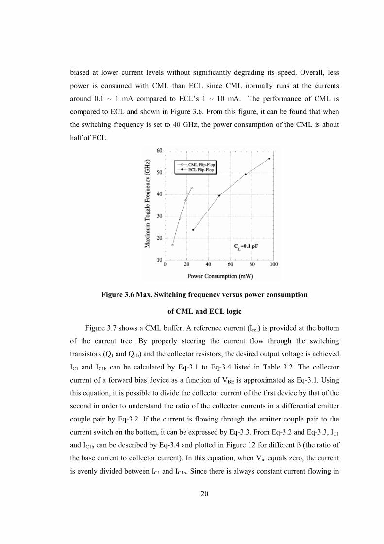
compared to ECL and shown in Figure 3.6. From this figure, it can be found that when
the switching frequency is set to 40 GHz, the power consumption of the CML is about
half of ECL.
Figure 3.6 Max. Switching frequency versus power consumption
of CML and ECL logic
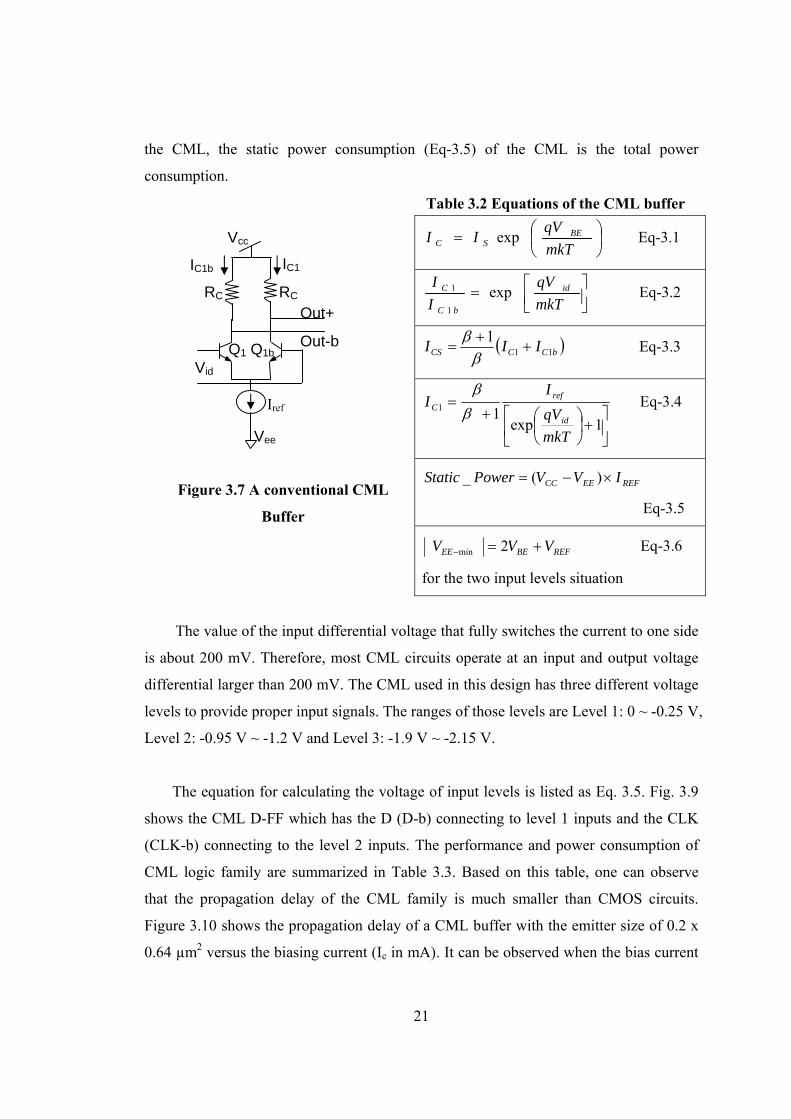
Figure 3.7 shows a CML buffer. A reference current (Iref) is provided at the bottom
of the current tree. By properly steering the current flow through the switching
transistors (Q1 and Q1b) and the collector resistors; the desired output voltage is achieved.
IC1 and IC1b can be calculated by Eq-3.1 to Eq-3.4 listed in Table 3.2. The collector
current of a forward bias device as a function of VBE is approximated as Eq-3.1. Using
this equation, it is possible to divide the collector current of the first device by that of the
second in order to understand the ratio of the collector currents in a differential emitter
couple pair by Eq-3.2. If the current is flowing through the emitter couple pair to the
current switch on the bottom, it can be expressed by Eq-3.3. From Eq-3.2 and Eq-3.3, IC1
and IC1b can be described by Eq-3.4 and plotted in Figure 12 for different ß (the ratio of
the base current to collector current). In this equation, when Vid equals zero, the current
is evenly divided between IC1 and IC1b. Since there is always constant current flowing in
21
the CML, the static power consumption (Eq-3.5) of the CML is the total power
consumption.
The value of the input differential voltage that fully switches the current to one side
is about 200 mV. Therefore, most CML circuits operate at an input and output voltage
differential larger than 200 mV. The CML used in this design has three different voltage
levels to provide proper input signals. The ranges of those levels are Level 1: 0 ~ -0.25 V,
Level 2: -0.95 V ~ -1.2 V and Level 3: -1.9 V ~ -2.15 V.
The equation for calculating the voltage of input levels is listed as Eq. 3.5. Fig. 3.9
shows the CML D-FF which has the D (D-b) connecting to level 1 inputs and the CLK
(CLK-b) connecting to the level 2 inputs. The performance and power consumption of
CML logic family are summarized in Table 3.3. Based on this table, one can observe
that the propagation delay of the CML family is much smaller than CMOS circuits.
Figure 3.10 shows the propagation delay of a CML buffer with the emitter size of 0.2 x
0.64 µm2 versus the biasing current (Ic in mA). It can be observed when the bias current
⎟⎠⎞
⎜⎝⎛=
mkTqVII BE
SC exp Eq-3.1
⎥⎦⎤
⎢⎣⎡=
mkTqV
II id
bC
C exp1
1 Eq-3.2
( )bCCCS III 111
++
=β
β Eq-3.3
⎥⎦
⎤⎢⎣
⎡+⎟
⎠⎞
⎜⎝⎛+
=1exp
11
mkTqVI
Iid
refC β
β Eq-3.4
REFEECC IVVPowerStatic ×−= )(_
Eq-3.5
REFBEEE VVV +=− 2min Eq-3.6
for the two input levels situation
Vcc
RC
Vid
Iref
Out+
Out-b
Vee
Q1 Q1b
RC
IC1b IC1
Figure 3.7 A conventional CML
Buffer
Table 3.2 Equations of the CML buffer
22
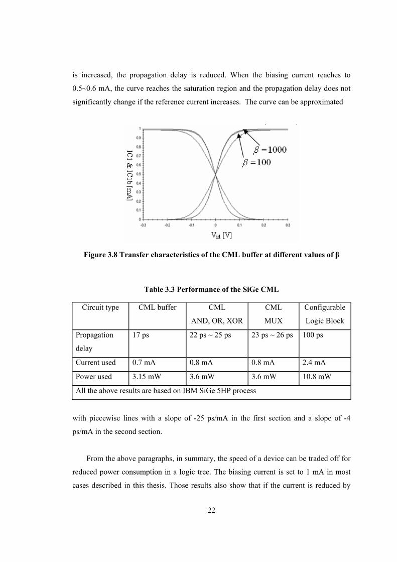
is increased, the propagation delay is reduced. When the biasing current reaches to
0.5~0.6 mA, the curve reaches the saturation region and the propagation delay does not
significantly change if the reference current increases. The curve can be approximated
Figure 3.8 Transfer characteristics of the CML buffer at different values of β
Table 3.3 Performance of the SiGe CML
Circuit type CML buffer CML
AND, OR, XOR
CML
MUX
Configurable
Logic Block
Propagation
delay
17 ps 22 ps ~ 25 ps 23 ps ~ 26 ps 100 ps
Current used 0.7 mA 0.8 mA 0.8 mA 2.4 mA
Power used 3.15 mW 3.6 mW 3.6 mW 10.8 mW
All the above results are based on IBM SiGe 5HP process
with piecewise lines with a slope of -25 ps/mA in the first section and a slope of -4
ps/mA in the second section.
From the above paragraphs, in summary, the speed of a device can be traded off for
reduced power consumption in a logic tree. The biasing current is set to 1 mA in most
cases described in this thesis. Those results also show that if the current is reduced by

23
half, for example to 0.5 mA, the power consumption can reduced by half with the
propagation delay increased by 2 ps. This design idea imitates the Power Saving Mode
CML circuit described later.
Figure 3.9 CML D-latch configuration with two input levels
Figure 3.10 Propagation delay of the CML buffer
with the emitter size of 0.2 x 0.64 µm.
Vcc RC
D
Iref
OutOut-b
Vee
Q1 Q1b
RC IC1b IC1
Q2 Q2b
CLK CLK_b
Level 1:
0 V ~ 0.25 V
Level 2:
0.95 V ~ 1.2 V
D-b
VREF

24
3.6 Difficulties of designing a CML high speed FPGA
The power consumption of the first SiGe CLB was about 10.8 mW, which is larger
than its CMOS competitors. To realize a large scale CML FPGA, some power-saving
strategies have to be applied. Four methods are provided to solve the power consumption
problem.
1. The first method is to reduce the reference current in the tree to decrease the static
power consumption by sacrificing the speed of the transistors. From Figure 3.5, the
cutoff frequency (120 GHz) of the 0.18 µm process has a maximum value when
reference current equals to 1.1 mA. If the current is reduced by half, 0.5 mA, the cutoff
frequency of the SiGe HBT only drops to 80 GHz which is a 35% reduction. This
implies that by compromising bandwidth of an HBT, the current can be reduced to lower
the power consumption of CML circuits.
2. Second, the power supply voltage can be reduced to further decrease the static
power consumption. Based on Eq. 3.5 in Table 3.2, if the power supply can be reduced
by half, the total power consumption can be decreased by half.
3. Third, by combining the logic in a circuit, the number of the CML trees can also
be decreased too.
4. Lastly, turning off unused circuits and combining some logic blocks in the Basic
Cell can further lower the power consumption.
The first strategy leads to future larger scale FPGAs. The second, third and last
strategies lead to a modified CLB design. Both designs improvements are described in
the following chapters.

25
4 Large Scale (16 x16 BC array) SiGe FPGA design
In this chapter, a 16 x 16 BC array SiGe FPGA with 2.8 V power is presented. The
detailed schematic, layout and design considerations are described. Figure 4.1 shows the
block diagram of the SiGe 16 x 16 BC array FPGA. It is designed to perform 4-bit logic
operations. Four sub-blocks are included; they are the FPGA core, input multiplexer
block, output selection block and oscillator.
Figure 4.1 Block diagram of the 16 x 16 array FPGA.
The input multiplexer block has two 4-bit MUXs used to multiplex the selected
external signals (Signal A and B) and the test signals generated from the frequency
divider. The outputs of four BC blocks can be selected as the FPGA output after the
selection of the output MUX. The detail functions of the blocks in Figure 4.1 are
explained in the following paragraphs.
4.1 The XC 6200 Basic Cell
A reduction in the number of CML trees per Basic Cell results in lower power
consumption for the entire design. Therefore, one of the goals is to simplify logic gates
of the Basic Cell in the Xilinx 6200 FPGA. The Basic Cell block diagram shown in
Figure 4.2 consists of input/output routing blocks and a Function Unit (FU). The input

26
routing block is composed of three 8:1 multiplexers (MUXs) to route the outputs from
the surrounding Basic Cells (coming from N, S, E, W) into the Function Unit. The RP
MUX routes the combinational signal and the sequential signals into the D-FF. The CS
MUX, which selects combinational or sequential logic, routes the chosen signals to the
output routing block, consisting of four 4:1 MUXs. The output routing block then routes
the signals to the neighboring Basic Cells. The Basic Cell schematic is redrawn and
shown in Figure 4.1.
4.1.1. Input routing block
The input routing block combines the logic functions of the 8:1 MUX and 4:1
MUX, shown in the gray blocks I and II of Figure 4.1 to a new MUX. In Figure 4.2, the
new input routing block separates the signals by their incoming directions. All the input
signals coming from the same direction (N, S, E and W) are connected to the same 4:1
MUX. For example, all signals originating east of a Basic Cell are connected to one 4:1
MUX. The 8:1 MUX in the original design is broken down into four 4:1 MUXs from all
directions, and the four 4:1 MUX outputs are combined with the output of the D-FF in a
second level 5:1 MUX. Advantages of this combination are reduction in circuit
complexity and propagation delay while maintaining full compatibility with the original
6200 configuration bit streams.
Figure 4.2 XC6200 Basic Cell.
RP
8:1
4:1
4:1
E, S, N
W, S, N
E, W, S
E, W, N
4:1
4:1
I
III
D-FF 4:18:1 CS
C
Q
IV
Function Unit (FU)
E
W
S
N
Input routing
block
Output routing
block
E, W, S, N
E4, W4, S4, N4
E, W, S, N
E4, W4, S4, N4
E, W, S, N
E4, W4, S4, N4
4:18:1
II

27
The MUXs used in the input routing block have been redesigned as well. The
general form of the new design circuit is shown in Figure 4.3. The differential input pair
Figure 4.3 Redesigned input routing block. Label Ce indicates
combinational logic (C) from the east.
Figure 4.4 General form of the new MUX design. The new input routing stage has
4:1 and 5:1 MUXs and the new output routing stage has 4:1 MUXs.
of transistors is connected to the drain of an NMOS switch. Only one pair can be
selected in a MUX, so with the use of a decoder the desired differential input pair can be

28
selected and the remaining pairs turned off to save power. The output MUXs have the
same configuration.
4.1.2. Function Unit (FU) in the new Basic Cell
In block III of Figure 4.2, the RP MUX was merged into the D-FF, thus further
reducing the number of CML trees. Since another input level for the RP selection control
is inserted into the D-FF, the CML tree will be taller. Reducing the height so that a
smaller power supply can be used is crucial. The schematic of the new D-Flip Flop after
merging with the RP MUX is shown in Figure 4.4 for Latch 1 and Figure 4.5 for Latch 2.
The main concepts of designing the new MUX focus on how to properly steer the
current into independent current trees. By adding a switch to the Vref transistor in the
CML tree, the entire tree can be turned off. In Figure 4.5 showing the Latch 1 design of
the new D-FF, if combinational data C (C+/ C-) is the desired input, the On-2 can be
disabled and On-1 can be turned on. To select sequential data Q (Q+/ Q-), the On-1
should be turned off and On-2 be turned on. With the use of the switches, the functions
of the RP MUX can be completely merged into the first latch. In Latch 2, there are two
current trees. However, only one current tree will be turned on at any given time, similar
to Latch 1. One tree is for the D-latch logic and the other is for “CLEAR” (CLR) to
directly pull down the output to the lowest voltage in the circuits. With this design, there
can be two input voltage levels with the power supply voltage equals to 2.5 V.
Figure 4.5 Latch 1 in the new D-FF design.

29
Figure 4.6 Latch 2 in the new D-FF design.
The CS MUX, shown in block IV of Figure 4.2, is used for selecting either
combinational logic (C+, C-) or sequential logic in the original design. With the new
input stage, this job is now done at the next Basic Cell’s input routing stage, so the CS
MUX can be removed from the Function Unit in the new Basic Cell to reduce the total
gate delay. The new Basic Cell structure is shown in Figure 4.7. It is created by
simplifying and combining the four blocks (I, II, III and IV) drawn in Figure 4.2. The
overall functions of the Basic Cell remain the same as in the original design to keep the
same bit stream and use the existing software (Xilinx 6200) to program them. After
Figure 4.7 Schematic of the BCII.

30
Figure 4.8 Layout of the Basic Cell
developing the new Basic Cell, the total number of current sources has been reduced
from 30 (14 CML trees, 8 pairs of the emitter followers) to 21 (13 CML trees, 4 pairs of
emitter followers) and the propagation delay has been reduced as well. The layout of the
new Basic Cell is shown in Figure 4.8 with the dimension of 230 x 170 mm2.
4.1.3. Dynamic shut down of unused circuits
The NMOS switches in every MUX and D-FF can be used to disable the unused
circuits. Thus, it can be used to shut down unused current trees in the programmed Basic
Cell to reduce power consumption. In the worst case (Basic Cell maximum usage case),
there will be no circuits that can be turned off.
In Case I, there is a combinational or sequential function enabled and no redirected
signals. The signals come in from the input routing block and passed to the Function
Unit (FU). In this case, there are 10 or 12 current trees turned on. In the second case

31
(Case II), the Basic Cell is programmed to perform sequential logic and the input signals
are also redirected to the output routing block.
Figure 4.9 Layout of the new Basic Cell
Table 4.1 Dynamic Routing Power Usage
Case I. Only combinational logic or sequential logic is used.
Case II. Sequential logic and redirection function are used.
Case III. Only redirection function is used.
Design Tree # Power Usage
BC Maximum Usage 21 100%
Case I (Comb./ Sequential Logic) 10 / 12 47.6% / 57.1%
Sequential, One Redir. 15 71.4%
Sequential, Two
Redir.
18 85.7%
Case II
Sequential, Three
Redir
21 100%
Case III 3 tree / dir 14.2% / dir
170um
230um
III
I
IV
I: Function unit.
II: Input routing block
III: Output routing
II
III

32
Based on how many signals are redirected, the numbers of the current trees enabled
are: 15 for one redirected signal, 18 for two redirected signals and 21 for three redirected
signals. The above results are summarized in Table 4.1.
4.2 Voltage Controlled Oscillator (VCO) in SiGe FPGA
In the 16 x 16 BC array FPGA, its clock is generated from a Voltage Control
Oscillator (VCO) which is a four-stage ring oscillator shown in Figure 4.10 (a). A
modified Gilbert mixer is used as its building block. This VCO can linearly interpolate
the signals received from the previous two stages. Each stage mixes the signals from
previous stage and the stage preceding that one. For example, the output signals of the
buffer B depend on the signals from A and D buffers. These signals are weighted by the
control signals of the mixer and summed by the pull-up resistors. The minimum
operating frequency is defined by the case when the leap signal is ignore, which is
shown in Figure 4.10 (b).
Figure 4.10 the VCO’s architecture (a) Feed Forward VCO block diagram. (b) The VCO running in the four stage configuration with the control voltage set to a minimum value. (c) The VCO in the two stage configuration at the maximum
control voltage.
The VCO’s maximum frequency can be achieved by ignoring the previous stage
signals. Thus, the oscillator runs as a two stage ring oscillator (Figure 4.10 (c)), which
has a higher frequency than 4-stage case (Figure 4.10 (b)). Figure 4.11 shows the
schematic of the VCO multiplexer. It linearly interpolates the signal from the previous
A
B
C
D
C C
D D
A A
B B
(a) (b) (c)

33
stage (A20, A21) and the buffer previous to that stage (B20, B21) through the control
voltage (C30, C31). Resistor Rb limits the operating range of the VCO, Re adjusts the
control voltage range and capacitor Cc defines the operating range. In the 16 x 16 FPGA,
the VCO was designed to run in the range between 7 and 13 GHz with the center
frequency at 10 GHz. Figure 4.12 shows the layout of the VCO which is symmetrical to
minimize unbalanced parasitic effects caused by different lengths of wires.
Figure 4.13 Block diagram of the input/output blocks and the FPGA core.
Figure 4.11 Schematic of the VCO buffer.
Z21 Z20
Rc Rc
Cc
Z11 Z10
A20 A21
B20 B21
Rb Rb
Re Re
C30 C31
Vcc
Vee
Figure 4.12 Layout of the VCO buffer.
MUX Emitter
follower
Output
4 x 4 BC block (BC-BLOCK)
1st area The output of the first 4 x 4 BC block
2nd area The output of the first row of 4 x 4 BC
3rd area The output of two row 4 x 4 BC block
4th area Four rows of 4 x 4 BC block to output
Input A
Input B
Output
MUX

34
4.3 Input multiplexer block, output selection blocks and FPGA core
The data flow of the FPGA is shown in Figure 4.13. The FPGA core, located in the
center, is constructed of five 4 x 4 BC arrays (BC-BLOCKs). Depending on the number
of BCs that an application needs, one of four portions of the BC array is activated. The
first portion is the first BC-BLOCK, the second portion is the first row of BC-BLOCKs,
the third portion is the first two rows of BC-BLOCKs and the last is the whole BC array.
The two input 4-bit signals (A and B) are routed to the first and second row of the BC
BLOCKs. Two MUX selection signals decide whether the internal or the external signals
are routed to the core. All outputs must be routed to an output MUX which connects to
the external pads.
4.4 Programming scheme in the Basic Cell and FPGA
To test this FPGA, it is very important to have a robust and simple programming
structure. There are several ways to program it. Using shift registers to transport data
into memory is one of the simpler methods. The advantages of using a shift register
structure are ease of scaling up, reduced timing constrains, and a relatively simplified
structure. The drawbacks are its circuit layout occupies more area than other memory
structures (DRAM) and the time to program all the memory cells is longer. In this FPGA,
we don’t need to care about the speed to program memory cells. Therefore, the shift
register structure was picked to program this SiGe FPGA chip.
4.4.1 Programming structure used in Basic Cell
The programming structure of the Basic Cell includes two parts. One is the shift
register and the other is the memory bank. Its schematic is shown in Figure 4.14. Since
this part doesn’t have to run at very high speed, the timing constrain of the clock is not
as critical as the FPGA core, however the signal strength of the clock and data must be
guaranteed. Therefore, repeaters have been placed to insure the clock reaches its logic
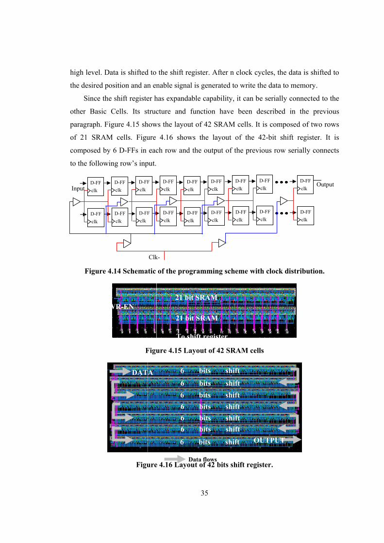
35
high level. Data is shifted to the shift register. After n clock cycles, the data is shifted to
the desired position and an enable signal is generated to write the data to memory.
Since the shift register has expandable capability, it can be serially connected to the
other Basic Cells. Its structure and function have been described in the previous
paragraph. Figure 4.15 shows the layout of 42 SRAM cells. It is composed of two rows
of 21 SRAM cells. Figure 4.16 shows the layout of the 42-bit shift register. It is
composed by 6 D-FFs in each row and the output of the previous row serially connects
to the following row’s input.
Figure 4.14 Schematic of the programming scheme with clock distribution.
Figure 4.15 Layout of 42 SRAM cells
Figure 4.16 Layout of 42 bits shift register.
6 bits shift
6 bits shift 6 bits shift 6 bits shift 6 bits shift 6 bits shift
6 bits shift
DATA
Data flows
OUTPUT
D-FF clk
D-FF clk
D-FF clk
D-FF clk
D-FF clk
D-FF clk
D-FF clk
D-FF clk
D-FF clk
D-FF clk
D-FF clk
D-FF clk
D-FF clk
D-FF clk
D-FF clk
D-FF clk
D-FF clk
D-FF clk
Clk-
Output Input
WR-EN 21 bit SRAM
21 bit SRAM
To shift register

36
The above circuits were simulated with a 500 MHz clock at a temperature of 50oC.
Figure 4.17 shows the simulation result of the 42-bit memory circuit. When WR-EN is
zero, the outputs of the 42 memory bits are all “one”. While the WR-EN changes to high,
the data is latched into the memory and programs the Basic Cell. Figure 4.18 shows the
simulation of the shift registers. The first four outputs are monitored. In those outputs,
the data is propagating from one flip flop to the next one.
4.4.2 Programming circuit in the 16 x 16 FPGA
There are two methods to program the configuration bit stream into an FPGA. The
first method is to use the DRAM structure. It has to deal with read (write) timing issues
which make the memory systems much more complicated to design. Another method is
to use the shift register structure to reduce the complexity of the memory structure and
shift the data stream to the corresponding memory positions. Figure 81 shows the
connection of a row of Basic Cell in the 16 x 16 FPGA. A long chain of shift registers
can be formed to increase the flexibility of the hardware scale. Data can be passed to
every Basic Cell to program desired functions. Then the data path is connected to the
input of next row of Basic Cell.
Figure 4.18 Simulation result of the
shift register output with input data
period of 800 ps.
Figure 4.17 Simulation of the 42-bit
memory.
37
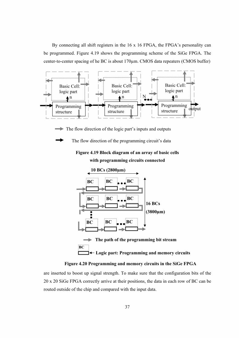
By connecting all shift registers in the 16 x 16 FPGA, the FPGA’s personality can
be programmed. Figure 4.19 shows the programming scheme of the SiGe FPGA. The
center-to-center spacing of he BC is about 170µm. CMOS data repeaters (CMOS buffer)
Figure 4.19 Block diagram of an array of basic cells
with programming circuits connected
are inserted to boost up signal strength. To make sure that the configuration bits of the
20 x 20 SiGe FPGA correctly arrive at their positions, the data in each row of BC can be
routed outside of the chip and compared with the input data.
10 BCs (2800µm)
BC BC BC
BC BC BC
BC BC BC
16 BCs
(3800µm)
Figure 4.20 Programming and memory circuits in the SiGe FPGA
The path of the programming bit stream
Logic part: Programming and memory circuits BC
The flow direction of the programming circuit’s data
The flow direction of the logic part’s inputs and outputs
N
Basic Cell: logic part
Programming structure
n
Basic Cell: logic part
Programming structure
n
Basic Cell: logic part
Programming structure
n
output

38
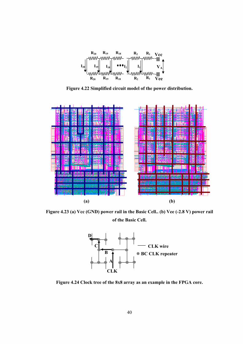
4.5 Power Rails design
In Figure 4.21 (a) and (b), the black and gray wires show the Vcc (0 V) and Vee (-
2.8 V) power rails. Since the voltage is gradually lost along the wires due to parasitic
elements, it is very important to design power rails that have no large voltage drop
between the ends of rails. Table 4.2 shows some important parameters of the SiGe
process. In order to get a good estimation of the power rail width, some assumptions
must be made;
1. The length of the Basic Cell is 170 µm with an additional 5 µm spacing to the next
Basic Cell. (L = 175 µm)
2. The thickness and width of the AM metal are both 4µm.
3. The current that each BC consumes is 1 mA (in the 8HP IBM model manual, fTmax can
be achieved at Ic = 1 mA).
4. All the current trees in the Basic Cell are on (22 current trees; 22 mA).
5. The voltage at the end of the power line is less than 2.79 V. The allowable voltage
droop is 1% since the input power is 2.8 V.
Vcc Vee
Figure 4.21 (a) Power rail in the FPGA core. (b) Power rail in each BC. (a)
Vcc
Vee
Power rail length: 175 μm
BC length: 170 μm
Req
Req
(b)

39
Table 4.2 Characteristics of the metal layers of the IBM 7 HP process
First, the equivalent resistance (Req) of the Basic Cell power rail can be calculated
by Eq-4.1. If the width of the power rail is w, Req will equal to 1.225/w Ω. Then Req is
applied to a simplified power droop model as illustrated in Figure 4.22. In the FPGA,
there are 16 BCs in each row and column. Each one is designed to have 1 mA currents
flowing in it. Therefore, the R1 to R20 equal to Req and I1 to I16 equal to 22 mA. Applying
those parameters to the model shown in Figure 4.22 and Eq-4.2, the width of the power
rails should be more than 68µm. To get less power droop on the rail, 75µm is selected
for the width in the FPGA core. Figure 4.23 shows the power rails in the Basic Cell.
Table 4.3 Equations for calculating power droop and power rail width.
Ω=⎟⎠⎞
⎜⎝⎛=⎟
⎠⎞
⎜⎝⎛×⎟
⎠⎞
⎜⎝⎛=
wwwl
tR seq
225.1175007.0ρ
Eq-4.1
( ) ( ) 2020191920221920
1121920
22...2...2)...(79.28.2
RIRIIRIIIRIIIIVA
×+×+++×++++×++++=−=
Eq-4.2
ρ = resistivity
t = thickness
l = conductor length,
w = conductor width
Req= the sheet
resistance (Ω/square)
Metal layers Design Width
(µm)
Thickness
(µm)
RS (Ω/square)
M1, Mx, MT, x = 2, 3, 4 0.5 ≤ M1 < 1.0
0.5 ≤ Mx
0.36 ± 0.05 0.07 ± 0.012
M1, Mx, MT, x = 2, 3, 4 < 0.5 0.31 ± 0.05 0.089 ± 0.018
LY ≥1.52 1.25 ± 0.13 0.023 ± 0.005
AM ≥ 4.0 4.0 ± 0.4 0.0070 ± 0.0015
40
Figure 4.22 Simplified circuit model of the power distribution.
(a) (b)
Figure 4.23 (a) Vcc (GND) power rail in the Basic Cell.. (b) Vee (-2.8 V) power rail
of the Basic Cell.
Figure 4.24 Clock tree of the 8x8 array as an example in the FPGA core.
CLK wire
CLK
BC CLK repeater A
B C
D
I20
R20 R1 Vcc
Vee R1 R2
R2
R20
R19
R19
R18
R18
I19 I18 I2 I1 VA

41
Figure 4.25 Schematic (a) and layout (b) of the clock repeater.
4.6 Clock and programming circuit clock distributions
To demonstrate the clock tree in the SiGe FPGA, an 8 x 8 BC array is used. The
clock distribution shown in Figure 4.24 is based on the H-pattern structure which
reduces the influence of parasitic effects and load effects to a minimum. Since the SiGe
FPGA runs at higher frequency (in the GHz range), avoiding clock skew is very
important. To alleviate the signal attenuation problem, repeaters are added to the clock
tree. The schematic and layout of the repeater composed of a Current Mode Logic (CML)
buffer and emitter followers are shown in Figure 4.25 (a) and (b). Figure 4.26 and 4.27
shows a test structure and simulation results of a clock repeater loaded with different
length wires (400 µm ~ 700 µm). One can observe that the output waveform of the 700
µm wire case starts to distort. Therefore, the clock repeater can deliver the signals
through a 700 µm wire (when the input signal frequency is at 10 GHz). Figure 4.26
shows the simulated waveforms of the repeater outputs loaded with one to five repeaters.
As more repeaters are added, the increase in the rise time is observed. Therefore, in the
20 x 20 FPGA, every repeater is loaded with only one repeater. Figure 4.28 shows the
post layout simulation result of the partial tree from point A through B and C to D (The
length of A, B, C, and D are 620, 360, 175 and 175 µm). In the same figure, the
Z21Z20
Rc
A11
Vcc
Vee
A10
Rc
(a) (b)

42
propagation delay between point A and D is 30.6 ps. The layout of the programming
circuit clock also follows the design methodology of the clock tree.
Figure 4.26 Test structure of the repeater driving capability. The loaded wire is varied from 400~700µm.
Figure 4.27 Simulation result of the clock repeater driving 400~700µm wire loads with the 10 GHz test signal.
Figure 4.28 Simulation result of the clock repeater loaded with one to five clock repeater loads.
Input CLK (10GHz)
400um wire load
500um wire load
600um wire load
700um wire load
One repeater loaded (Red curve) Four repeaters loaded
Three repeaters loaded
Two repeaters loaded
Five repeaters loaded
(Blue curve)
Repeater
400um
700um Repeater
RepeaterRepeater

43
Figure 4.29 Propagation delay between A, B, C and D
in clock tree shown in Figure 4.30
Figure 4.30 Clock distribution of the SiGe FPGA
30.52ps
Point A (10GHz)
Point B
Point C
Point D

44
Figure 4.31 Detail clock distribution circuit in the 4 x 4 BC array.
To minimize the clock skew of the clock tree, the delays in the clock tree must be
correctly matched. This is usually accomplished by matching the driver and transmission
line delays in each stage. Since this chip uses CML as the building logic, its differential
nature suppresses induced phase noise. Therefore, the H-tree structure is adopted. Figure
4.30 shows the clock distribution of the SiGe FPGA. The clock distribution also uses
differential signaling to avoid introducing cross talk between wires and phase noise. It is
separated into two parts shown in Figure 4.30. Part A is the symmetric part (16 x 16
Basic Cell array). Part B is the asymmetric part. Since the FPGA repeatedly uses the
same reconfigurable cell (Basic Cell), the load of each terminal at the end of the clock
tree in part A is the same. Figure 4.30 shows the clock tree in the 4 x 4 BC array. In the
clock distribution tree, all paths are designed to have the same length in order to have the
clock signal arrive at every BC at the same time. Regarding Part B, it has an asymmetric
layout which makes it more difficult to match the length of interconnects all the same,
though each net has identical loads. Therefore, its layout should be designed more
carefully. The method which tries to match the length of wires was used.
CLK_in
Repeater
Clock path

45
4.7 SiGe FPGA Basic Cell Configuration
The detailed data stream of the basic cell is described in this part. Then the data
stream of the SiGe FPGA is mentioned. Figure 4.31 shows the schematic of the BC. It is
separated into three parts. For each stage, input routing stage, configuration logic block
and output routing stage, the configuration is explained. Table 4.4 lists the function table
of the BCII which is the same with XC 6200 FPGA. First, the configuration of the input
routing stage is described.
Figure 4.32 Schematic of the BCII.
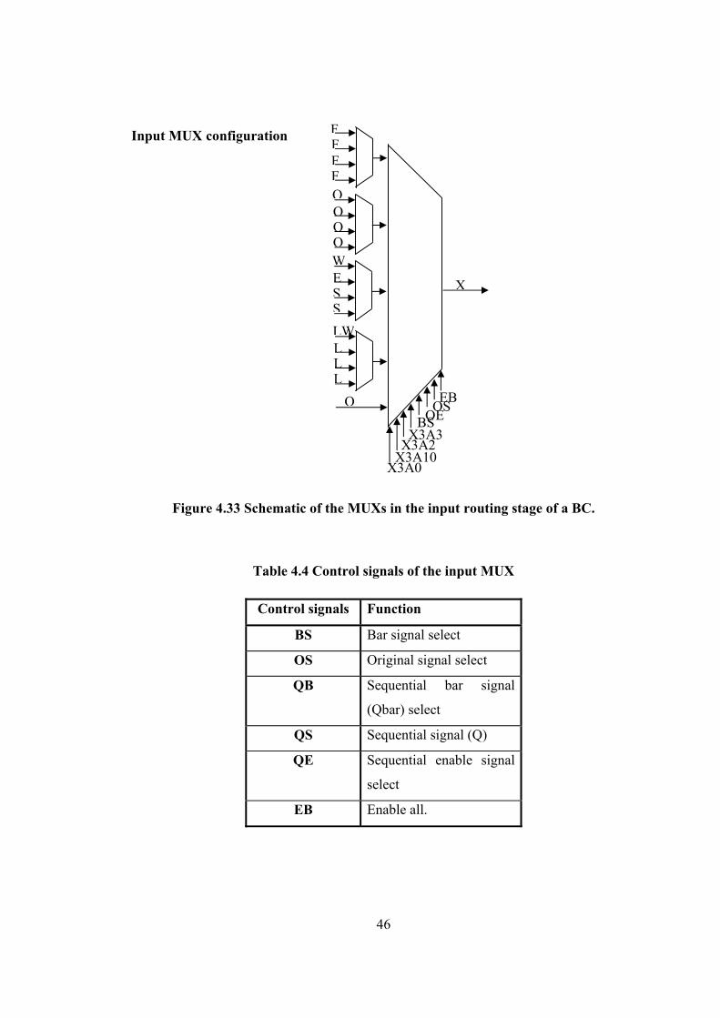
Figure 4.32 shows the schematic of the MUX used in the Input Routing Stage. The
configuration the MUXs are listed in Table 4.4~4.8. Table 21 lists the input signals of
the Input Routing Stage. Table 4.4 shows the configuration of the MUXs. Figure 4.33
shows the Output Routing Stage. Table 4.5 and 4.6 show the input selection of the
combinational and sequential logic functions and Table 4.7 shows the configuration of
the output signals. Table 4.8 shows the bit arrangement of a BC.
SetWout
SetEout
SetSout
SetNout
X1
X2
X3
46
Input MUX configuration
Figure 4.33 Schematic of the MUXs in the input routing stage of a BC.
Table 4.4 Control signals of the input MUX
Control signals Function
BS Bar signal select
OS Original signal select
QB Sequential bar signal
(Qbar) select
QS Sequential signal (Q)
QE Sequential enable signal
select
EB Enable all.
X3A0 X3A10 X3A2
X3A3BS
F
F
Q
Q
X
FF
QQQ
SSEW
LLLLW
OSQEEB

47
Table 4.5 Configuration of the input MUX: X1, X2 and X3
Table 4.6 Selection of the combinational and sequential operations
P Q
Combinational logic select (CS_en) 1 0
Sequential logic select (QS_en) 0 1
X3A00 X3A10 X3A20 X3A30 X3ABS X3AQS X3AQE
FW 1 1 1 1 0 X 0
FE 0 1 1 1 0 X 0
FS 1 0 1 1 0 X 0
FN 0 0 1 1 0 X 0
QW 1 1 0 1 0 X 0
QE 0 1 0 1 0 X 0
QS 1 0 0 1 0 X 0
QN 0 0 0 1 0 X 0
WW 1 1 1 0 0 X 0
EE 0 1 1 0 0 X 0
SS 1 0 1 0 0 X 0
NN 0 0 1 0 0 X 0
LW 1 1 0 0 0 X 0
LE 0 1 0 0 0 X 0
LS 1 0 0 0 0 X 0
LN 0 0 0 0 0 X 0
Output
invert
X X X X 1 X 0
Sequential
input -Q
X X X X X 0 1
Sequential
input -Qbar
X X X X X 1 1

48
Table 4.7 Selection of the CLB combinational or sequential outputs
Enable X direction F output (FZx) Enable sequential outputs (QZx)
CEnbX 1 X
QEnbX X 1
Note: X indicates the directions to the east (E), west (W), north (N) and south (S)
Output MUX configuration
SetXout [00, 03]
Figure 4.34 Configuration of the MUX bused in the Output Routing Stage.
Table 4.8 Configuration of the MUX of Output Routing Stage.
A00 A10 A20 A30
FW 1 1 1 0
FS 0 1 1 0
FN 1 0 1 0
QW 0 0 1 0
QS 1 1 0 0
QN 0 1 0 0
WW 1 0 0 0
SS 0 0 0 0
NN 1 1 1 1
FWFSFNQW
QNWWSSNN
QS Xout
A00 A10
A20 A30

49
Since the combinational and sequential outputs are directly routed to neighbor cells, the
output MUX has been modified to handle the redirected signals. The setting of the
redirected signals is listed in Table 4.9. For example, if a designer wants to select the
input signal from the West (FW), the configuration bits for the Xout MUX must be set to
1110.
Table 4.9 shows the bit stream of the BCII. There are 42 configuration bits in the
BC. Convenience for the layout of BC, the order of the bits has not been arranged to be
in the sequence as listed in tables.
Table 4.9 Bit pattern of the Basic Cell
0 1 2 3 4 5 6 7 SRAM-out SetWout00 SetWout10 SetWout20 SetWout30 SetSout00 SetSout10 SetSout20 SetSout30
SRAM-outb SetWout01 SetWout11 SetWout21 SetWout31 SetSout01 SetSout11 SetSout21 SetSout31
Function Output MUX West setup Output MUX South setup
8 9 10 11 12 13 14 15 SRAM-out X2B00 X2B10 X2B20 X2B30 X2BBS X3ABS P R SRAM-outb X2B01 X2B11 X2B21 X2B31 X2BOS X3AOS X X
Input Routing Stage X2 and X3 setup. Combinational/
Sequential
logic selection
16 17 18 19 20 21 22 23 SRAM-
out CEnbS CEnbN CEnbE CEnbW X3AQE X2BQE QEnb
S
QEnbN
SRAM-
outb X X X X X X X X
Combinational output signals enable X3
setup
X2
setup
Sequential
output signals
enable
50
24 25 26 27 28 29 30 31
SRAM-
out
QEnbE QEnbW X3A30 X3A20 X3A10 X3A00 X1C00 X1C10
SRAM-
outb
X X X3A31 X3A21 X3A11 X3A01 X1C01 X1C11
Input Routing Stage X3 setup.
32 33 34 35 36 37 38
SRAM-
out
X1C20 X1C30 SetEout30 SetEout20 SetEout10 SetEout00 SetNout30
SRAM-
outb
X1C21 X1C31 SetEout31 SetEout21 SetEout11 SetEout01 SetNout31
Input Routing
Stage X1 setup.
Output Routing Stage output direction setup.
39 40 41
SRAM-out SetNout20 SetNout10 SetNout00
SRAM-outb SetNout21 SetNout11 SetNout01
Contd.
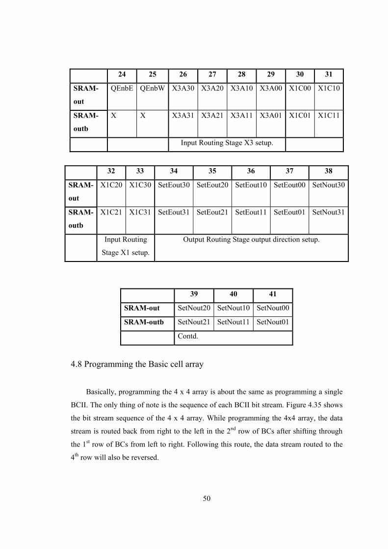
4.8 Programming the Basic cell array
Basically, programming the 4 x 4 array is about the same as programming a single
BCII. The only thing of note is the sequence of each BCII bit stream. Figure 4.35 shows
the bit stream sequence of the 4 x 4 array. While programming the 4x4 array, the data
stream is routed back from right to the left in the 2nd row of BCs after shifting through
the 1st row of BCs from left to right. Following this route, the data stream routed to the
4th row will also be reversed.

51
Figure 4.35 Configuration data path in the 4x4 BC array
Figure 4.36 Block diagram and data stream path of the 8 x 8 BC array.
Fig. 4.37 is the schematic of the external programming circuit which was realized
by an FPGA board. Lpm_rom7 is the memory that stores all the data to be sent to the
FPGA chip. There is also another circuit connecting the FPGA board to the FPGA chip
to transfer the output voltage of the board from (0V, 5V) to (-2.8V, 0V). This circuit is
realized by simple voltage dividers.
Vcc! Vref Vee20!

52
PIN_91VCC
CLK INPUT
PIN_45VCC
EN INPUT
PIN_53
VCCCLR INPUT
PIN_101outOUTPUT
clk_enOUTPUT
PIN_86clkoutOUTPUT
agbOUTPUT
PIN_95clkou1tOUTPUT
q[7..0]OUTPUT
NO
T
inst
4
AND2
inst3
NO
T
inst
5
D FLIP-FLOPS
2D2PRN1CLK
1D1PRN
2CLK2CLRN
1CLRN1QN
2Q2QN
1Q
7474
inst8 D FLIP-FLOPS
2D2PRN1CLK
1D1PRN
2CLK2CLRN
1CLRN1QN
2Q2QN
1Q
7474
inst7 D FLIP-FLOPS
2D2PRN1CLK
1D1PRN
2CLK2CLRN
1CLRN1QN
2Q2QN
1Q
7474
inst9
VCC VCC VCC
up counterclock
clk_en
aclr
q[7..0]
lpm_counter0
inst1
AND2
inst6
unsigned compare
datab[]=167dataa[7..0]
clockaclr
agb
lpm_compare1
inst2
address[7..0]outclock
q[0]
lpm_rom7
inst
Figure 4.37 Programming Circuit
4.9 Pin assignments of the 16 x 16 FPGA
Figure 4.38 shows the pin arrangement of the new 16-pin probe. There are 4 low
speed signal pins and 6 high speed pins. To avoid cross talk among the signals and from
other noise sources, the high speed probes are placed between power pads. Figure 4.39
shows the power probe to deliver power to the 16 x 16 FPGA. It has 10 pins on it.
Among them, there are 4 pairs of Vcc-Vee pins and 2 low speed signal pins on both ends.
Each power pin can deliver 1A. The total current of each power probe can deliver 8A.
Since there are two power probes, the total current delivering to the 16 x 16 FPGA is
16A. The detail specification of the test probes can be found in the www.ggb.com.
Figure 4.39 shows the final 16 x 16 FPGA layout with the power rails.

53
Figure 4.38 Pin arrangement of the 16-pin probe used in the 16 x 16 SiGe FPGA.
Figure 4.39 Pin arrangement of the 10-pin power probe used
in the 16 x 16 SiGe FPGA.
4.10 layout, programming sequence and power consumption
The layout of the SiGe 16 x 16 FPGA is shown in Figure 4.40. The center part is
the 16 x 16 BC array, with two 10 pads and two 16 pads on four sides. The length of the
chip is 2.85 mm x 3.8 mm.
Figure 4.41 shows the programming timing diagram. In the first cycle (Period A)
the FPGA core is disabled by clearing the data left in the memory and shift register
circuit to zero. Then the shift register starts to load the bit stream (Period B1). After
P Power pad 1 Vcc!
S Signal pad G Power pad 2 Vee!
10 pin probe
S P G P G PG G P S
Low speed signal pins
Low speed signal pins
16 pin probe
S S P S S P G P G S S G S S S S
P Power pad 1
Vcc!S Signal pad G Power pad 2
Vee!
Low speed signal pins
Low speed signal pins
High speed signal pins
High speed signal pins
High speed signal pins

54
finishing shifting data, the Write-EN is activated and the data is loaded into the memory
(Period B2). Then the FPGA starts to function by turning on the Read-EN (Period C). By
using this scheme, the CMOS part and the bipolar will not be activated at the same time
to avoid over driving the FPGA.
Figure 4.40 16 x 16 FPGA array programming structure
Figure 4.41 Timing diagram of the SiGe FPGA
A: Initialization period
B1: Programming bit stream period
B2: Loading bit stream period
Sel +
Sel - A B1 C B2
FPGA
core A
B
C
DE
2.85mm
3.8mm

55
This FPGA circuit is composed of CMOS and Bipolar parts. The CMOS logic is not
consuming power when it reaches a stable state. The power dissipation of the CMOS is
ignored here. Assuming all the current trees in the FPGA are turned on, the approximate
power consumption can be calculated. The power consumption of subsections is also
shown Table 4.10. Normally, when the FPGA is programmed, not all of the logic
circuits perform functions. Based on the estimation and calculation described in Chapter
3, the least power consumption is 3.55 W. Other cases are also summarized in the same
table.
Table 4.10 Estimated power consumption of the different Basic Cell configurations
Design Usage Estimated power
consumption
BC Maximum Usage 100% 25 W
Case I (Comb./Sequential Logic) 47.6 % / 57.1% 11.9 W / 14.3 W
Sequential, One Redir. 71.4 % 17.9 W
Sequential, Two Redir. 85.7 % 21.4 W
Case II
Sequential, Three
Redir.
100 % 25 W
Case III 14.2% / dir 3.6 W

56
5 the 16 x 16 SiGe FPGA Test and a New Chip Design
5.1 the 16 x 16 FPGA chip test
To demonstrate functions of the 16 x 16 FPGA, a test plan has been developed.
With the limited signal pins, the test plan is divided into two parts, the high speed and
low speed part.
5.1.1 Test plan of the high-speed part of the FPGA and LFSR
An LFSR is a state machine composed of a shift register with the signal from its
output fed back through an EX-OR gate to its input. If an LSFR is initialized to a non-
zero value and its serial input is tied off to logic zero, and if the feedback taps
correspond to a primitive polynomial, the cycle by cycle transition of states goes through
all possible combinations, except the all-zero state in a pseudo-random order.
Figure 5.1 Pseudorandom binary sequences.
Figure 5.2 Schematic of a four bit linear feedback sequences register (LFSR).
XOR
D Q
R
D Q
R
D Q
R
D Q
R
CLK RST
CH1 CH2 CH3 CH4
Repetitive pattern

57
The main purpose of the high-speed part of the chip shown in Figure 5.3 is to test
the GHz signals and data generated by the SiGe BCs. To use the Built-in Self-Test
(BIST) technique, an LFSR (Linear Feedback Shift Register) is added to provide a build-
Figure 5.3 Test circuitry of the 16 x 16 SiGe FPGA.
High speed input and output signals.
in signal source. An n bit LSFR will cycle through 2n-1 states before repeating the
sequence. In the 16 x 16 FPGA, a 4-bit LFSR is used. The outputs of the LFSR are
connected to the north inputs of the 4 x 4 block on the top-left corner. To provide the
sampling signals to the scope, an additional circuit is needed as a trigger signal to the
sampling scope. To make sure all blocks can be tested, the outputs in each 8 x 8 array
are routed to external pins.
Additional inputs, X1 and X2 are added to provide more input resources. All
signals are shown in Figure 5.1. Figure 5.4 shows the pin arrangement of the high-speed
signals of the 16 x 16 FPGA.
4x4 Array
LFSR CLK /N LFSR trigger
Input X1 (external)Input X2 (external)
Signal output 1 Signal output 2
Signal output 3 Signal output 4
Signal output 5 Signal output 6
Signal output 7Signal output 8
Signal output 10 Signal output 9
VCO
VCO output
/N VCO trigger
(LFSR eye-diagram trigger)

58
Figure 5.4 Pin assignment of the high speed (> 10 GHz) signals.
1 and 2: Outputs of the first 4 x 4 array on the top-left corner. 3 and 4: Outputs of the top-left 8 x 8 array.
5 and 6: Outputs of the top-right 8 x 8 array. 7: Outputs of the LFSR trigger.
8 and 9: Outputs of the bottom-left 8 x 8 array. 10: Outputs of the VCO trigger (fVCO/64).
11 and 12: Outputs of the bottom-right 8 x 8 array.
1
2
3
4 5
67
8
910
11
12

59
Figure 5.5 Input / Output arrangement of the programming data.
5.1.2 Test plan of the low speed part in the new FPGA
The main purpose of having the low signal test part is test the CMOS clock tree and
programming circuits. Figure 5.4 shows the low speed signal test plan. The data outputs
1~11, of the 4 x 4 and 8 x 8 arrays are routed to the external pins to make sure the
programming circuits work well. The tapered buffer is used to drive the output to the
pins. In general, one can always add inverters to the end of a path without changing its
function.
Figure 5.6 Schematic of the tapered buffer driving a 180 μm wire
the sizes of the inverters in the tapered buffer are incremented 4 times compared to its
previous stage. Figure 5.6 shows the tapered buffer used in the data path of the
Data input Data output
1x 3x 9x 27x
Wire length: 180 μm
C
4x4
Arrays
Data_output 1
Data_output 2 Data_output 4
Data output 5
Data_output 6
Data output 7
Data_output 8
Data output 9
Data_output 10
Data output 11

60
programming circuits. Figure 5.7 shows the pin assignment of the low speed signals of
the 16 x 16 FPGA.
Figure 5.7 Pin assignment of the low speed (> 1 GHz) inputs and outputs.
1: Data output of the first two rows in the top-left 4 x 4 array. 2: Data output of the second two row of BC in the top-left 4 x 4 array.
3. Programming circuit: CLR 4. Programming circuit: WR_BAR.
5. Data input. 6. Low speed external input signal.
7. Data output of the top-right 8 x 8 array. 8. Data output of the bottom-right 8 x 8 array.
9. CLK of the programming circuit.
5.1.3 Test procedure
To test the CMOS programming circuits, a CMOS FPGA with memory
programmed by its software can be used to generate the required signals. Figure 5.8
1
23 4
5
6
7
9
8

61
shows the test blocks that used in the SiGe FPGA test. The data stream of the SiGe
FPGA can be generated before storing to the memory in the CMOS FPGA. The data
stream is passed to the FIFO to synchronize with the CMOS_CLK and shift out the data
stream to the Data_in of the programming circuits in SiGe FPGA.
Figure 5.9 Test blocks on programming the SiGe FPGA configuration
with an FPGA board
5.2 16 x 16 SiGe FPGA Test Results
The first several tests shows that global clock signal generated by the VCO is not
transmitted to all the basic cells and LFSR correctly, which might be because the input
resistance of the clock pin on each basic cell is not big enough and therefore lower the
input signal voltage level. Now the test plans can not be executed on this chip.
However, the following tests show that the chip is still working well in the sequential
mode.
1. 8-stage ring oscillator
To generate a clock signal, an 8-stage ring oscillator is constructed by programming
7 basic cells as bypass repeaters and 1 basic cell as an inverter (Fig. 5.10). Fig. 5.11
shows the frequency of the oscillator is 1.5273GHz.
CMOS FPGA
Memory FIFO
CLK CMOS CLK
DATA
WR_bar
16 x 16 FPGA
Data_input
CMOS_CLK
Data_out

62
Figure 5.10. 8-stage Ring Oscillator Test Circuitry
Figure 5.11 8-stage Ring Oscillator Test Result

63
The basic cells in the bypass repeater mode do not contain any logic part and
therefore are the fastest units of this loop. The number of CML’s used in an inverter ( or
any other logic function) is twice of bypass repeaters, which means, the delay time cost
in the inverter (or any logic function) can be estimated to be around twice of the delay
time cost in the bypass repeater.
For the 8-oscillator loop, we have
GHzyx 5273.1/1)7(2 =+ (1)
Where x is the time cost in the bypass repeater, and y is the time cost in the inverter.
2. 2-stage ring oscillator
To find out x and y, a 2-stage ring oscillator is constructed by programming a
repeater (not in bypass mode for the signal from a certain direction can not be
transmitted in the bypass mode back to the same direction) and an inverter in a loop.
Fig.18 shows the frequency of the oscillator is 2.98493GHz. Then the second equation is
GHzyx 98.2/1)(2 =+ (2)
Figure 5.12. 2-stage Ring Oscillator Test circuitry

64
Figure 5.13 2-stage Ring Oscillator Test Result
Solve equation (1) and (2), we have
x=34ps, and y=84ps.
Or,
1/x=28.76GHz, and 1/y=11.94Hz.
The fact that repeater and inverter logic are realized successfully shows that the
FPGA chip works as expected, since all other logic functions are configured in the same
way. As a bypass repeater, a basic cell can work at up to 28.76GHz, and as any logic
functions unit, such as MUX, XOR, etc, it can run up to 11.94GHz.

65
5.3 The New 16 x 16 FPGA chip design
The 16 x 16 FPGA chip tested was designed by Dr. Jong-ru Guo at the end of 2005.
It was the first working FPGA chip of this project, while it still has several shortcomings:
1. Vdd is supplied by positive voltage, which adds more noise to the circuit.
2. The buffer used between each two basic cell memories is an inverter, which
converts the polarity of the data.
3. There is no high speed input signal.
4. There is no external clock signal.
5. LFSR is too long from the VCO, which might be the reason that LFSR doesn’t
work.
The author fixed these problems by doing the following updates:
1. Switch the pads of power and grand, including the power and grand rails
inside the chip.
2. Add another inverter between each two basic cells’ memories to make it a
buffer.
3. Change the two input (X1 and X2) to the high speed pad.
4. Change one of the high speed output pad to an external clock signal input.
5. Setup an internal oscillator by using one basic cell’s bypass mode, which can
be used as a high speed internal signal.
Now this new 16 x 16 chip has already been fabricated, and will be ready to test.
5.4 Future work
To get higher goal of the project, the following acts can be made in the future:
1. Move the whole design into 8HP or even 9HP technology, which will cost
less power and get higher frequency.
2. Add switches in each Basic Cell to show down those non-working basic cells,
so that the power consumption will be decreased farther.

66
3. Fig. 2.8 and Table 2.2 show that one basic cell can’t perform a simple
NAND logic, but AND is working well. So adding another bit to determine
whether to convert the polarity of the output will solve this problem.

67
References [1] Michael John and Sebastian Smith, “Application-Specific Integrated Circuits”,
Addison-Wesley VLSI System Series
[2] John F. McDonald et al, “Reconfigurable FPGA’s in the 1-20 GHz Bandwidth with
HBT BiCMOS”, Proceedings of the first NASA/ DoD Workshop on Evolvable
Hardware
[3] Bryan Goda et al, “SiGe HBT BiCMOS FPGAs for high speed reconfigurable
computing” IEE Proc. Computer and Digital Technology, vol 147. NO.3, May 2000
[4] Jong-ru, Guo, “A 16X16 Basic-Cell High Speed Silicon Germanium Field
Programmable Gate Array” , Ph.D. Thesis, Rensselaer Polytechnic Institute, Oct. 2005
[5]John D. Cressler, “SiGe HBT Technology: A New Contender for Si-Based RF and
Microwave Circuit Applications”, IEEE Tran. on Microwave Theory and Techniques,
VOL. 46, NO. 5, May, 1998.
[6] Flash Comm. www.flashcomm.com.
[7] IEEE spectrum SiGe cross section figure.
[8] Okan Erdogan, “A Three-Port Pipelined Register File Implemented Using a SiGe
HBT BiCMOS Technology”, Ph.D. Thesis, Rensselaer Polytechnic Institute, Dec 2006
[9] Chao You, “A High-Speed, Low Power SiGe BiCMOS FPGA with New Features for
Applications”, Ph.D. Thesis, Rensselaer Polytechnic Institute, May 2005
[10] Kuan Zhou, “ LOW-POWER MULTI-GHZ SIGE FPGAS FOR
RECONFIGURABLE COMPUTING”, Ph.D. Thesis, Rensselaer Polytechnic Institute,
July 2004
[11] Raminderpal Singh, David L Harame and Modest M. Oprysko. “Silicon
Germanium Technology, Modeling and Design”. IEEE press
[12] D. Lammer, “IBM SiGe hits 350 GHz”, Microwave Engineering,
www.mwee.com/mweenews/showsarticle, Nov 02, 2002.
[13] Greg Freeman et al, “40 Gb/s Circuits Built from a 120 GHz fT SiGe Technology”,
IEEE Journal of Solid State Circuits, vol. 9. September, 2002
[14] Y. Taur and T. H. Ning, “Fundamentals of Modern VLSI Devices”, Cambridge
University Press, 1998

68
[15] John D. Cressler, “SiGe HBT Technology: A New Contender for Si-Based RF and
Microwave Circuit Applications”, IEEE Tran. on Microwave Theory and Techniques,
VOL. 46, NO. 5, May, 1998
[16] D. L. Harame, et al “Current Status and Future Trends of SiGe BiCMOS
Technology” IEEE Trans. On Electron Device, VOL. 48, NO. 11, Novemember, 2001
[17] J. Sitch, et al, “HBT IC’s for OC-192 equipments”, Int. J. High Speed Electron
System, Special Issue on High Speed Circuits for Light wave Communications, K. C.
Wang, Ed., 1999
[18] Ken Martin, “Digital Integrated Circuit Design”, Oxford University Press Inc.
[19] Kiyoshi Ishii et al, “4-bit Multiplexer/Demultiplexer Chip Set for 40-Gbit/s Optical
Communication Systems” IEEE Trans. On Microwave Theory and Techniques, VOL. 51,
NO. 11, 2003.
[20] Samuel A. Steidl, “ A 32-Word by 32-bit Three-port Bipolar Register File
Implemented Using a SiGe HBT BiCMOS Technology”, Ph.D. Thesis, Rensselaer
Polytechnic Institute, May 2001
[21] XC6200 data sheet.
[22] Keiji Kishine et al, “A High Speed, Low-Power Bipolar Digital Circuit for Gb/s
LSI’s: Current Mirror Control Logic”, IEEE Journal of Solid State Circuits, Vol.32 No.
2, Februrary, 1997
[23] Gerd Schuppener, et al, “Investigation on Low-Voltage, Low Power Silicon Bipolar
Topology High Speed Digital Circuits”, IEEE Journal of Solid State Circuits, Vol. 35,
No. 7, July 2000
[24] Xilinx Power consumption work sheet V 1.5, http://www.xilinx.com/cgi-
bin/powerweb.pl.
[25] T. W. Krawczyk, et al, “SiGe HBT serial transmitter architecture for high speed
variable bit rate intercomputer networking”, IEE Proc. Circuits Devices Syst.
[26] IBM 7HP design manual.
[27] G. Freeman et al. “40 Gb/s Circuits Built From a 120-GHz fT SiGe Technology”
IEEE Journal of Solid-State Circuits, Vol. 37, NO. 9, 2002, pp1106-1114.
[28] Behzad Razavi ‘Design of Integrated Circuits for Optical Communications”,
pp12~14, McGraw-Hill, 2003.

69
[29] Anatha Chandrakasan, William J. Bowhill and Frank Fox. “Design of high-
performance Microprocessor Circuits”, IEEE Press
[30] Self test text book.
[31] Jong-Ru Guo, et, al, "A high speed Reconfigurable Gate Array for Gigahertz
Applications", Annual Symposium on VLSI, p 124~129. May, 2005
[32] Xilinx Virtex data sheet.
[33] Xilinx Power consumption work sheet V 1.5, http://www.xilinx.com/cgi-
bin/powerweb.pl.
[34] Cadence design manual, “Diva Product Notes”
[35] Neil H. E. Weste, David Harris, “CMOS VLSI DESIGN”, Pearson Education Inc.
[36]. Ralph Niederberger, et al. “High speed Supercomputer communications in
Broadband Networks”