Embed Size (px)
Citation preview

politecnico di milano
department of physics
doctoral program in physics
Silicon-Germanium Heterostructures forSilicon Photonics Applications
Doctoral Dissertation of:
Jacopo Frigerio
Supervisor:
Dr. Giovanni Isella
Tutor:
Prof. Franco Ciccacci
The Chair of the Doctoral Program:
Prof. Paola Taroni
2014 - XXVI Cycle

2

Contents
Introduction 7
The interconnect bottleneck . . . . . . . . . . . . . . . . . . . . . . . . 8
Optical interconnects . . . . . . . . . . . . . . . . . . . . . . . . . . . . 10
Receiver circuit . . . . . . . . . . . . . . . . . . . . . . . . . . . . 11
Transmitter circuit . . . . . . . . . . . . . . . . . . . . . . . . . . 11
Silicon photonics . . . . . . . . . . . . . . . . . . . . . . . . . . . . . . 13
Silicon based light sources . . . . . . . . . . . . . . . . . . . . . . 13
Silicon modulators . . . . . . . . . . . . . . . . . . . . . . . . . . 15
The role of germanium . . . . . . . . . . . . . . . . . . . . . . . . . . . 17
Ge based light sources . . . . . . . . . . . . . . . . . . . . . . . . 18
Ge based modulators . . . . . . . . . . . . . . . . . . . . . . . . . 19
1 Germanium Bandstructure Engineering 23
1.1 Germanium Bandstructure . . . . . . . . . . . . . . . . . . . . . 23
1.2 Strain . . . . . . . . . . . . . . . . . . . . . . . . . . . . . . . . . 25
1.2.1 Biaxial strain . . . . . . . . . . . . . . . . . . . . . . . . . 27
1.2.2 Origin of biaxial strain in Ge-on-Si technology . . . . . . 30
1.2.3 Uniaxial strain . . . . . . . . . . . . . . . . . . . . . . . . 32
1.3 N-type doping . . . . . . . . . . . . . . . . . . . . . . . . . . . . 34
1.3.1 Free carrier absorption . . . . . . . . . . . . . . . . . . . . 35
1.4 Quantum Confinement . . . . . . . . . . . . . . . . . . . . . . . . 36
1.4.1 Quantum Confined Stark Effect . . . . . . . . . . . . . . . 37
3
4 CONTENTS
2 Heteroepitaxial growth of SiGe alloys 39
2.1 Introduction . . . . . . . . . . . . . . . . . . . . . . . . . . . . . . 39
2.2 LEPECVD . . . . . . . . . . . . . . . . . . . . . . . . . . . . . . 39
2.3 Growth modes . . . . . . . . . . . . . . . . . . . . . . . . . . . . 42
2.4 Strain related phenomena in heteroepitaxial growth . . . . . . . 43
2.5 Growth of pure Ge on Si . . . . . . . . . . . . . . . . . . . . . . . 46
2.6 Deposition of Ge/SiGe MQW . . . . . . . . . . . . . . . . . . . . 47
2.6.1 Virtual substrates . . . . . . . . . . . . . . . . . . . . . . 47
2.6.2 Strain compensation in multilayers . . . . . . . . . . . . . 48
3 Ge/SiGe MQW for silicon photonics 51
3.1 Optical modulation at 1.3 µm . . . . . . . . . . . . . . . . . . . . 51
3.1.1 Introduction . . . . . . . . . . . . . . . . . . . . . . . . . 51
3.1.2 Sample growth and charachterization . . . . . . . . . . . . 52
3.1.3 Photocurrent Measurements . . . . . . . . . . . . . . . . . 54
3.1.4 The role of Γ-∆ scattering . . . . . . . . . . . . . . . . . . 55
3.2 Electro-Refractive effect in Ge/SiGe MQW . . . . . . . . . . . . 57
3.2.1 Introduction . . . . . . . . . . . . . . . . . . . . . . . . . 57
3.2.2 Sample growth and characterization . . . . . . . . . . . . 58
3.2.3 Device processing . . . . . . . . . . . . . . . . . . . . . . . 60
3.2.4 Experimental charachterization of the ER effect . . . . . . 61
3.2.5 Evaluation of the device performance . . . . . . . . . . . . 66
3.3 Ge/SiGe MQW photonic interconnection . . . . . . . . . . . . . 67
3.3.1 Introduction . . . . . . . . . . . . . . . . . . . . . . . . . 67
3.3.2 Sample growth and charachterization . . . . . . . . . . . . 67
3.3.3 Device processing and Measurements . . . . . . . . . . . . 69
4 Hyghly strained Ge micro-bridges 75
4.1 Introduction . . . . . . . . . . . . . . . . . . . . . . . . . . . . . . 75
4.2 Strain Enhancement . . . . . . . . . . . . . . . . . . . . . . . . . 76
4.3 Sample growth and characterization . . . . . . . . . . . . . . . . 76
CONTENTS 5
4.3.1 Thermal strain . . . . . . . . . . . . . . . . . . . . . . . . 76
4.4 Fabrication of the micro-bridge . . . . . . . . . . . . . . . . . . . 80
4.5 Raman measurements . . . . . . . . . . . . . . . . . . . . . . . . 82
4.6 Photoluminescence measurements . . . . . . . . . . . . . . . . . . 82
4.7 Gain calculation . . . . . . . . . . . . . . . . . . . . . . . . . . . 84
5 Carrier lifetime study in Ge-on-Si epilayers 87
5.1 Introduction . . . . . . . . . . . . . . . . . . . . . . . . . . . . . . 87
5.2 N-type doping calibration . . . . . . . . . . . . . . . . . . . . . . 88
5.2.1 PH3/GeH4 ratio . . . . . . . . . . . . . . . . . . . . . . . 88
5.2.2 Growth temperature . . . . . . . . . . . . . . . . . . . . . 89
5.3 Influence of doping on the lifetime . . . . . . . . . . . . . . . . . 90
5.4 Influence of the Ge/Si interface on the lifetime . . . . . . . . . . 93
Conclusions 95
Bibliography 99
Acknowledgments 109

6 CONTENTS

Introduction
Silicon photonics addresses the study and the technological application of silicon
as an optical medium for generation, transmission, modulation and detection
of light. It has been envisioned that silicon photonics will solve the intercon-
nect bottleneck of CMOS technology, by the on-chip integration of silicon based
optical interconnects with standard electronic elements. This technology has
already shown its tremendous potential in the first demonstration of board-to-
board optical interconnetion [1] in which an integrated transmitter chip with
hybrid silicon lasers and an integrated receiver chip based on germanium pho-
todetectors were connected by optical fibers to realize a 50 Gbit s−1 optical link.
Nowadays, commercially-available Si-based 100 Gbit s−1 optical transceiver are
the first choise for data communication in server clusters or data storage centers
[2],[3], neverthless, the on-chip integration of silicon photonics still remains far
to be reached. First of all, energy consumption targets for optical modulators
are very aggressive, 100 fJ/bit for off-chip distances, 10’s of fJ/bit for high den-
sity off-chip connections and a few fJ/bit for on-chip applications [4]. Wideband
silicon modulators based on the Mach-Zender architecture typically have much
larger energy compsumption due to the large device size [5],[6] and new low-
energy approches involving electro-optic polymers still suffers of high insertion
losses and temperature sensitivity. Moreover, for future on-chip optical applica-
tions, an efficient, monolithically integrated laser source is required. A Ge-on-Si
laser source has already been demonstrated both in optical [7] and electrical
[8] pumping configuration, nevertheless the threshold current and the output
7

8 CONTENTS
power are still far from the required values for on-chip applications [9]. In the
last decade, the envisioned integration of optics and electronics has driven a
remarkable developement of silicon and germanium-on-silicon technology, open-
ing new paths for applications not related to interconnetions, such as optical
sensors for biological applications [10] and solar cells. The first aim of this thesis
is to study and develop high performance and low-energy intensity and phase
modulators based on Ge/SiGe multiple quantum wells (MQW) by exploiting
the Quantum Confined Stark Effect. The presented results show that Ge/SiGe
MQW have a strong potential as a new possible material platform for the future
developement of silicon photonics.The second aim is the developement of highly
tensile strained Ge-on-Si devices for efficent light emission.
The interconnect bottleneck
With the developement of the 22 nm Intel Tri-Gate Transistor Technology [11]
(See. Fig1), the Moore law will be respected for many years to come, never-
theless, the electrical interconnection problem is expected to became a major
limitation within a few years. The first problem to be considered in relation
to the electrical wiring is the interconnect density. As the complexity of the
Figure 1: Image of the 22nm 3D Tri-Gate transistor. Source: Intel website.
CONTENTS 9
integrated circuit increases, the available space tends to be filled with wiring
and as a consequence, their dimensions have to be scaled, but the capacity of
the wire in terms of transmission capacity cannot increase. This limitation can
be understood in terms of a simple physical model. At the gigahertz working
frequency typical of modern integrated circuits, interconnections are mainly lim-
ited by their RC product. If the cross-sectional size of the wire is reduced, its
resistance will increase. Moreover, the capacitance per unit-lenght will remain
unchanged, since it scales only logarithmically with the ratio of the wire size
to wire separation. Briefly, by scaling the wires in all three dimensions, it is
not possible to increase the number of bits per second that they can carry. For
simple on/off signaling, the transmission capacity of an electrical line can be
written approximately as:
B 6 B0A
L2(1)
Where A is the cross-sectional area of the wiring, L is the lenght and B0 is a
constant (v 1016 bits per seconds).The dimensionless A/L2 ratio is what makes
the transmission capacity independent of the size of the system. In addition,
the physics of electrical lines leads to many other problems for signal integrity,
such as the ”cross-talk” between adjacent lines through capacitive coupling and
reflections in the trasmission line.The second problem related to electrical inter-
connection is power dissipation. The performance of modern integrated circuits
is increasingly limited by power dissipation, wihch is also becoming ecologically
significant [12]. There are many sources of power dissipation in information
processing. Basically, every logical operation must consume energy, and, in ad-
dition to these operations, there are other dissipations coming from leakage and
subtreshold currents. For every unit of energy spent with logical operations,
there will be a multiplier factor due to the power supply and to the sinking
of thermal dissipation. However, the dominant contribution to the energy con-
sumption can be attributed to the electrical interconnections, and this energy is
associated to the charging and discharging the transmission lines[13]. In electri-
cal communication, the whole line has to be charged up to at least the signaling

10 CONTENTS
voltage, with an energy consumption:
Es 6 ClV2l (2)
Where Cl is the line capacitance and Vr is the signaling voltage. The capaci-
tance of a typical line is around 2pF/cm, and since it is low sentitive to scaling,
the only way to reduce the energy consumption is the reduction of the signaling
voltage.
Optical Interconnects
Optical interconnects offer many advantages with respect to electrical intercon-
nects, in particular regarding signal timinig and integrity. Optical channels are
characterized by low dispersion, allowing the transimission of pulses through
long distance without significant broadening, and the propagation velocity have
a reduced temperature dependence. Wavelength division multiplexing increases
the transmission capacity of a single channel. The ”cross-talking” is not de-
pendent on the bit rate, since it is much lower with respect to the carrier fre-
quency, and physical phenomena such as signal reflection are much easier to be
minimized. Optics has already replaced electrical wiring in long distance com-
munications, and, as mentioned before, also in board-to-board commnications
for some very important markets, however, interconnection density and power
consumption are critical parameters to be considered in order to move the op-
tical interconnect technology to shorter distance, such as on-chip applications.
Optics does not have resistive losses in the transmission line, meaning that the
bit rate is not limited by a relation such as the one expressed in equation 1.1 for
electrical wiring. For this reason, optics is particularly attractive for long lines
with limited cross sections. Regarding the power consumption, optics have an
important advantage since it uses quantum sourcing and detection of the signal,
whitout any need of line charging. The relevant energy is the one required to
discharge the capacitance Cd of the photodetector and the electrical input to

CONTENTS 11
which it is connected by the signal voltage:
Ep > CdVr~ωe
(3)
where the voltage ~ω is equal to the photon energy in eV. Let’s now examine
in some detail the energy targets for optics. In order to be competitive with
near future electric interconnections, the system energy per bit should be
50-200 fJ/bit, and even lower to meet demands out to 2022 according to ITRS
projections. An optical system requires a transmitter driver circuit, an optical
output device, an optical channel and a photodetector, with the relative circuit.
Receiver circuit
By considering a photodetector integrated with a transistor, we have to estimate
the total capacitance given by the photodetector capacitance and the one of the
transistor’s gate. A photodetector with an area of a few square micrometers
with a thickness around 100 nm should have capacitances of a few fF. On the
other hand, the gate capacitance of an NMOS transistor is 1.2 fF/µm for the 32
nm node. Ge-on-Si photodetectors with the required capacitance have already
been demonstrated [14],[15]. The total involved energy for such a system is in
the femtojoules range.
Transmitter Circuit
The target energy for the transmission circuit is around 2-10 fJ/bit, as discussed
in [9]. We can consider a transmitter circuit as a system involving a light source
and a modulator. Up to now, a state-of -the-art laser has an energy consumption
of 5.5 fJ/bit [6]. This laser is made of III-V semiconductors, and there is a
general problem regarding the growth of III-V materials on silicon due to the
lattice mismatch, which leads to crystal defects. Such defects are known to be
detrimental for the device performance. III-V lasers can be bonded on silicon
through evanescent coupling between the laser and the silicon waveguide, but
such a complicated fabrication process is not suitable for large integration. The

12 CONTENTS
preferred solution for on-chip application is the developement of a light source
based on group IV elements. As mentioned before, Ge-on-Si laser have been
demonstrated in electrically pumped configuration, however the performances
of such device are still far from what required, not only in terms of energy
consumption. Also off-chip laser sources have been considered. Even if there
is a problem related to the coupling of light source to the chip, there are also
several advantages such as the removal of additional power dissipation from the
chip, and the possibility to optimize the laser performances without considering
all the integration problems. For modulators, we have two broad categories,
refractive and absorptive. Refractive modulators are limited by the absence of
an high speed physical effect capable to give refractive index variations higher
than 10−3. With such a small variation, considering a Mach-Zendher modulator,
device lenght of hundreds of micrometers are required in order to obtain a π
phase shift, leading to energy consumptions in the range of hundreds of fJ/bit
or higher. In order to have compact refractive modulators, the use of resonators
or slow light is required. However it has to be considered that the tuning of
such devices are obtained by thermal power, thus increasing the overall power
consumption. Modulators based on electroabsorption works by changing the
absorption spectrum of a semiconductor by appying an electric field to it. The
two physical effects behind electroabsorption are the Franz-Keldysh (FK) effect
for bulk semiconductors and the quantum confined Stark effect (QCSE) for
quantum confined structures such as quantum wells. Both effects require electric
fields in the range of 1-10 V/µm, easily obtainable in a reverse biased p-i-n
structure in which the intrinsic region is made by the bulk or quantum well
materials. These effects are able to enhance the optical absorption below the
bandgap energy, in particular the FK effect is charachterized by a long and
smooth absorption tail, with absorption coefficients in the range of some hundred
cm−1. Devices based on the FK effect tipically require a long interaction lenght.
QCSE gives more abrupt spectral features, with typical absorption coeffient
of several thousands cm−1. The QCSE is a very strong physical effect, thus
the realization of modulators with a lenght of a few micrometers is feasible.

CONTENTS 13
Moreover, the QCSE modulators are expected to work at very high data rate,
since it has been theorized that the fundamental speed limit of this effect is
below the picosecond[17].In these devices the energy consumption is the energy
required to charge up the active volume to the operative voltage. Devices with
energies of a few tens of femtojoules have already been demonstrated[18].
Silicon Photonics
In this section the operation principles and state of the art silicon photonics
devices is presented. For the pourposes of this thesis, the review will be focused
on light sources and modulators. The first two subsections are dedicated to
silicon, while the third one is focused on germanium based devices.
Silicon based light sources
Si and Ge are indirect bandgap semiconductors. Free electrons tend to stay in
the lower valleys of the conduction band (X for Si and L for Ge) which are not
aligned in the reciprocal space with free holes in the valence band. Radiative
recombination can occur only if a third particle, a phonon, is ivolved in order to
fulfill the momentum conservation, thus leading to slow optical transition rates.
Two important non-radiative recombination processes are the Auger recombi-
nation and the free carrier absorption (FCA). Auger recombination is a three
particle process in which an electron or an hole is raised to an higher energy
level by absorbing the energy relased by an electron- hole recombination. The
rate is proportional to the free carrier density and inversely proportional to the
bandgap. In FCA an electron or an hole can be raised to higher energy levels
by directly absorbing a photon. Also FCA is proportional to the carrier density,
and in majority carriers devices such as lasers, or in heavily doped materials, it
is usually higher than the material gain. For both these processes, the excited
carriers relax the excess energy by emitting phonons and they have lifetimes
much shorter with respect to radiative recombination.

14 CONTENTS
Figure 2: Scheme of the energy band diagram and major carrier transition
process in Si and InP. Reproduced from [19].
Silicon Raman laser
The Raman effect is based on the inelastic scattering of a photon by an optical
phonon. When a photon is absorbed by an atom at a certain vibrational state, it
is raised to an intermediate higher state. The excess energy is usually released
by the emission of a photon with the same energy, bringing back the system
to the ground state, but it is also possible to see weak additional components
with lower and higher energies with respect to the incident photon. These
components are due to the absorption or emission of optical phonons, namely
the Stokes and anti-Stokes transitions. Stimulated Raman scattering occurs
when the medium is irradiated symultaneously with a pump beam and a signal
beam which is resonant with the Stokes transition. A pulsed silicon Raman
laser was demonstrated for the first time in 2004[21] followed one year later by
the demonstration of continuous wave operation[22].Up to now, state of the art
Si Raman lasers have a threshold power of 20 mW with an output power of 50
mW, with a spectal purity well beyond best the performance of laser diodes.

CONTENTS 15
Integration of III-V lasers on Si
Another interesting approach in order to realize a silicon compatible light source
is based on the growth of III-V materials such as GaAs or InP on silicon. It is
very well known that the lattice and thermal expansion coefficient mismatches
between these materials and silicon lead to an high density of threading dis-
locations (TD) (108-1010 cm−2) in the grown material. Numerous approaches
have been proposed in order to reduce the TD density, such as special surface
treatement[23] and strained superlattices [24]. Recently SiGe buffer layers[25]
have been used to realize GaAs based continuous wave lasers on silicon at room
temperatures, but their reliability is still a problem for applications.
Hybrid silicon lasers
A promising approach, already employed in off-chip optical interconnection
devices, is based on the bonding of III-V semiconductors on an silicon-on-
insulator(SOI) substrate. In this way it is possible to combine very high quality
materials with the lattice mismatch silicon substrate. Silicon passive optical cir-
cuits are processed before the transfer, and the III-V structures are fabricated
after the transfer by standard optical litography. The first demonstration of
an hybrid Fabry-Perot laser was done in 2006[26], followed in the last years by
an optimization of the device architectures, leading to the realization of lasers
with very high performances with treshold currents in the range of mA and mW
output powers[27].
Silicon modulators
The physical effects traditionally employed in semiconductors to obtain electro-
refraction (ER) or electro-absorption (EA) are the Pockels effect, the Kerr effect
and the FK effect. Unfortunately these effects are very weak in pure silicon at
the telecommunications wavelengths[28], thus alternative methods are required.
One possibilty, since silicon has a very large thermo-optic coefficient, is to ex-
ploit the thermo-refractive effect. However it is not suitable for high speed

16 CONTENTS
Figure 3: Cross section of the first high speed silicon modulator. Reproduced
from [30].
applications. The most common effect in order to obtain modulation in sil-
icon is the plasma dispersion effect. By changing the carrier density in the
material, it is possible to change both the refractive index and the absorption
coefficient at a given wavelength. The charge density can be changed electri-
cally by injection, accumulation or depletion. The first breakthrough in silicon
modulation technology came in 2004, when the first high speed modulator was
demonstrated[29]. The device, capable of operating speed up to 1GHz, works
by the accumulation of free carriers on the two sides of a dieletric layer inside
a waveguide(See fig.3). The performances of carrier accumulation based modu-
lators were later optimized. Recently Lightwire reported a modulator with an
operating speed up to 10 Gbit/s at an extinction ratio1 of 9dB, with an active
lenght of 480µm[31]. Another technique based on the manipulation of the car-
rier density is the carrier depletion, in which the light beam propagates through
the junction of a reverse biased p-n structure. This technique is particularly
suitable for high speed operation, at the expense of the extinction ratio. Liu
et al[32] reported transmission rate up to 40 Gbit/s in a device operating in
1extinction ratio is defined as the ratio of Imax, the intensity transmitted when the mod-
ulator is adjusted for maximum transmission, to Imin, the intensity transmitted when the
modulator is adjusted for minimum transmission.It is quoted in decibels and expressed as
10log(Imax/Imin)

CONTENTS 17
carrier depletion mode. Devices based on carrier accumulation or depletion are
typically used in a Mach-Zehnder interferometer with a device lenght of hudreds
of micrometers or even millimiters, thus the power consumption, which is in the
range of hundreds of fJ/bit, is still to high for on-chip applications. A possible
strategy in order to reduce the device footprint is the use of resonant structures
such as ring resonators, which were introduced by Xu[33]. The device, based
on carrier injection in a p-i-n structure, had a data rate of 1.5 Gbit/s. Further
improvement moved the data rate up to 16 Gbit/s with an extinction ratio of
8dB. The ring diameter was only 12 µm, giving a footprint smaller than any
Mach-Zehnder modulator. Mach-Zehnder interferometers with a reduced lenght
were also fabricated by using photonic crystals[34]. Both ring resonators and
photonic crystals are very effective in reducing the device footprint and the en-
ergy consumption while keeping high performances in terms of extinction ratio
and data rate. However they suffer of a strong temperature dependence and
very narrow working spectrum.
The role of germanium
It has been envisioned that germanium, thanks to its photonic properties and
its compatibility with CMOS technology, will open the path through on-chip
applications of silicon photonics. Ge and Si have significant mismathces both
in lattice parameter and in thermal expansion coefficient, nevertheless the het-
eroepitaxial growth of Ge on Si has undergone a remarkable developement in the
last decade. Nowadays, high quality Ge crystals grown on Si can be obtained
with several growth techniques, including Chemical Vapor Deposition (CVD),
molecular beam epitaxy (MBE) and low energy plasma enhanced CVD (LEP-
ECVD). Initially, the interest in germanium for silicon photonics appication was
driven by the possibilty to exploit the direct gap absorption to realize compact
and efficient monolithic photodetectors on Si. The absortpion edge of Ge is
located at 0.8 eV, thus both the 1.3µm and the 1.55 µm optical fibers windows
can be covered by this material. Photodetectors with performances comparable

18 CONTENTS
to III-V semiconductors have already been demonstrated both in p-i-n[35] and
avalanche[36] configurations.
Ge based light sources
Despite its indirect band structure, germanium can be turned into an efficient
light emitter by using heavy n-type doping and tensile strain, as theorized by
Liu et al. [37].N- type doping is able to fill the L valley with electrons coming
from the impurities, enhancing the efficiency of carrier injection into the Γ val-
ley under external pumping [38] (See fig 4). On the other hand tensile strain
is able to reduce the band gap and the energy separation between the direct
and the indirect conduction band minima. The effect of tensile strain on the
photoluminescence of germanium was experimentally demonstrated by Cheng.
et al [39]. The authors used induced a biaxial tensile strain up to 0.36% by
an external mechanical stressor and they observed a remarkable enhancement
of the direct-gap related radiative recombination as the tensile strain was in-
creased(See fig 5). The first demonstration of direct-gap related electrolumines-
Figure 4: Room temperature photoluminescence spectra of phosphorous doped
germanium [38].

CONTENTS 19
Figure 5: Room temperature photoluminescence spectra of tensile strained ger-
manium [39].
cence was demonstrated in 2009 by Sun et al.[40]. In this work, a Si-Ge-Si p-i-n
light emitting diode was fabricated and light emission at 0.77 eV was reported.
The first demonstration of laser operation in Ge-on-Si was done in 2010 by the
MIT group[7]. In their work, the authors exploited n-type doping and tensile
strain to achieve lasing in an optically pumped Ge on Si waveguide. Two years
later, the same group realized the first Ge on Si electrically pumped laser[8].In
this work, the n-type doping was increased in order to achieve an higher gain,
thus compensating for the additional losses caused by the electrical pumping.
However, the laser have a very high current density treshold of 290 kA/cm−2,
which is very far from what required for silicon photonics applications.
Ge based modulators
Germanium exhibit a strong FK effect, that can be used to realize compact and
efficient intensity modulators. Recently a SiGe FK modulator with a device
lenght of only 50µm was demonstrated[41]. The device shows an extinction
20 CONTENTS
ratio of 7 dB and a modulation speed up to 1 GHz. Thanks to the small device
lenght, the energy consumption was as low as 50 fJ/bit. The breakthrough in
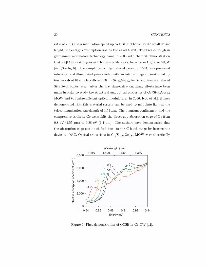
germanium modulators technology came in 2005 with the first demonstration
that a QCSE as strong as in III-V materials was achievable in Ge/SiGe MQW
[42] (See fig 6). The sample, grown by reduced pressure CVD, was processed
into a vertical illuminated p-i-n diode, with an intrinsic region constituted by
ten periods of 10 nm Ge wells and 16 nm Si0.15Ge0.85 barriers grown on a relaxed
Si0.1Ge0.9 buffer layer. After the first demonstration, many efforts have been
made in order to study the structural and optical properties of Ge/Si0.15Ge0.85
MQW and to realize efficient optical modulators. In 2006, Kuo et al.[43] have
demonstrated that this material system can be used to modulate light at the
telecommunication wavelength of 1.55 µm. The quantum confinement and the
compressive strain in Ge wells shift the direct-gap absorption edge of Ge from
0.8 eV (1.55 µm) to 0.88 eV (1.4 µm). The authors have demonstrated that
the absorption edge can be shifted back to the C-band range by heating the
device to 90oC. Optical transitions in Ge/Si0.15Ge0.85 MQW were thoretically
Figure 6: First demonstration of QCSE in Ge QW [42].

CONTENTS 21
investigated by tight-binding[44] and by 8-band k.p [45]. Also the polarization
dependence of the absorption spectra was theoretically [46] and experimentally
[47] investigated. In [47] Chaisakul et al. compared the QCSE from the first two
excitonic transitions (HH1-cΓ1 and LH1- cΓ1) as a function of light polarization
by photocurrent measurements performed on planar waveguides. They observed
that for an incident light with TE polarization both the HH1-cΓ1 and LH1- cΓ1
transitions are present, while for an incident light with TM polarization only
the LH1- cΓ1 absorption peak is visible. Despite the higher optical losses at
lower wavelength, the LH1- cΓ1 transition is more efficient by a factor 3 with
respect to the HH1- cΓ1 transition for intensity modulation [48]. High speed and
low power consumption in a waveguide integrated electro-absorption modulator
was also recently demonstrated [18]. In this work the authors reported 23 GHz
modulation speed with a power consumption of only 15 fJ/bit from a 3µm wide
90µm long Ge/SiGe waveguide. Ge/SiGe MQW are nowadays cosidered very
promising in order to realize high performance silicon compatible modulators,
expecially because of their extremely low power consumption.

22 CONTENTS

Chapter 1
Germanium Bandstructure
Engineering
1.1 Germanium Bandstructure
Germanium is a group IV element with a diamond lattice structure, charac-
terized by the tetragonal coordination of each atom with its near-neighbours
of the same unit cell. The valence band, which is originated by a linear com-
bination of p-type orbitals, consists of three distinct bands: the heavy holes
(HH) band, the light holes (LH) band and the split-off (SO) band, which lies at
lower energies because of the spin-orbit interaction. The HH and LH bands are
degenerate at the Γ point, which is the top of the valence band. The conduc-
tion band of germanium is far more complicated, because it is originated from
a composition of spherical s-type orbitals and from strongly directional p-type
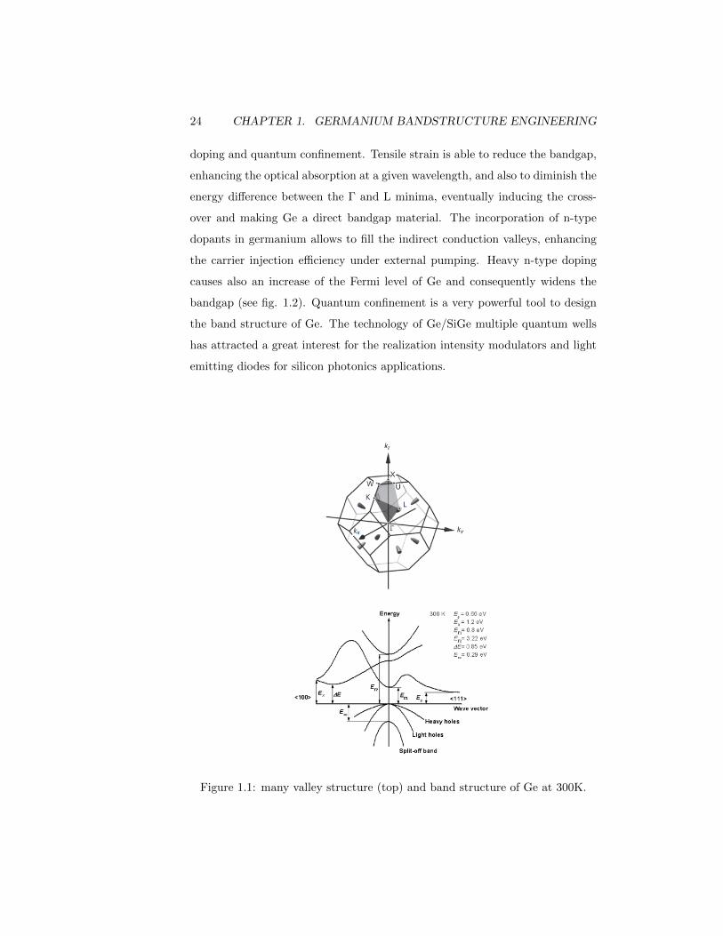
and d-type orbitals. The conduction band has four minima located in the L
point at k =< 111 >, with an energy gap EgL=0.66 eV and another minimum
located at the Γ point with an energy gap EgΓ=0.8 eV (See Fig. 1.1).The en-
ergy difference between the two minima is very small, only∆E = 0.14eV . The
band structure of germanium can be engineered by using strain, heavy n-type
23
24 CHAPTER 1. GERMANIUM BANDSTRUCTURE ENGINEERING
doping and quantum confinement. Tensile strain is able to reduce the bandgap,
enhancing the optical absorption at a given wavelength, and also to diminish the
energy difference between the Γ and L minima, eventually inducing the cross-
over and making Ge a direct bandgap material. The incorporation of n-type
dopants in germanium allows to fill the indirect conduction valleys, enhancing
the carrier injection efficiency under external pumping. Heavy n-type doping
causes also an increase of the Fermi level of Ge and consequently widens the
bandgap (see fig. 1.2). Quantum confinement is a very powerful tool to design
the band structure of Ge. The technology of Ge/SiGe multiple quantum wells
has attracted a great interest for the realization intensity modulators and light
emitting diodes for silicon photonics applications.
Figure 1.1: many valley structure (top) and band structure of Ge at 300K.

1.2. STRAIN 25
Figure 1.2: Schematic of the effect of tensile (biaxial) strain and n-type doping
on the band structure of Ge.
1.2 Strain
Strain in crystals is created by deformation and it is defined as a relative lattice
displacement. The strain state is expressed by a 3×3 matrix, the strain tensor:
ε =
εxx εxy εxz
εyx εyy εyz
εzx εzy εzz
(1.1)
Elastic strain in crystals is always the response to an applied stress, which can
be expressed with the following 3×3 matrix, the stress tensor:
σ =
σxx σxy σxz
σyx σyy σyz
σzx σzy σzz
(1.2)
Stress and strain tensors both have only six independent components and they
can be represented as a six elements column vectors. They are related through
26 CHAPTER 1. GERMANIUM BANDSTRUCTURE ENGINEERING
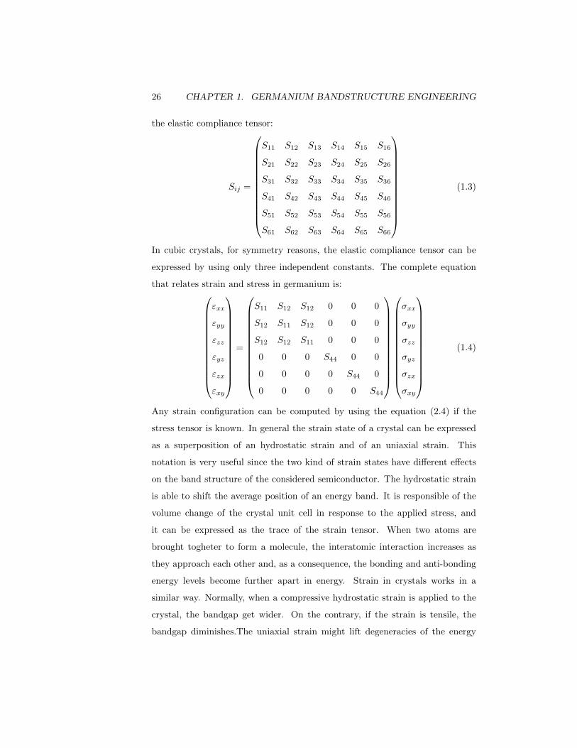
the elastic compliance tensor:
Sij =
S11 S12 S13 S14 S15 S16
S21 S22 S23 S24 S25 S26
S31 S32 S33 S34 S35 S36
S41 S42 S43 S44 S45 S46
S51 S52 S53 S54 S55 S56
S61 S62 S63 S64 S65 S66
(1.3)
In cubic crystals, for symmetry reasons, the elastic compliance tensor can be
expressed by using only three independent constants. The complete equation
that relates strain and stress in germanium is:
εxx
εyy
εzz
εyz
εzx
εxy
=
S11 S12 S12 0 0 0
S12 S11 S12 0 0 0
S12 S12 S11 0 0 0
0 0 0 S44 0 0
0 0 0 0 S44 0
0 0 0 0 0 S44
σxx
σyy
σzz
σyz
σzx
σxy
(1.4)
Any strain configuration can be computed by using the equation (2.4) if the
stress tensor is known. In general the strain state of a crystal can be expressed
as a superposition of an hydrostatic strain and of an uniaxial strain. This
notation is very useful since the two kind of strain states have different effects
on the band structure of the considered semiconductor. The hydrostatic strain
is able to shift the average position of an energy band. It is responsible of the
volume change of the crystal unit cell in response to the applied stress, and
it can be expressed as the trace of the strain tensor. When two atoms are
brought togheter to form a molecule, the interatomic interaction increases as
they approach each other and, as a consequence, the bonding and anti-bonding
energy levels become further apart in energy. Strain in crystals works in a
similar way. Normally, when a compressive hydrostatic strain is applied to the
crystal, the bandgap get wider. On the contrary, if the strain is tensile, the
bandgap diminishes.The uniaxial strain might lift degeneracies of the energy
1.2. STRAIN 27
bands, depending on the relation between the strain direction and the position
of the singular points in the bandstructure of the considered semiconductor.
The average energy of the band is not affected by this strain component. A
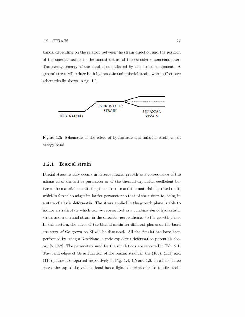
general stress will induce both hydrostatic and uniaxial strain, whose effects are
schematically shown in fig. 1.3.
Figure 1.3: Schematic of the effect of hydrostatic and uniaxial strain on an
energy band
1.2.1 Biaxial strain
Biaxial stress usually occurs in heteroepitaxial growth as a consequence of the
mismatch of the lattice parameter or of the thermal expansion coefficient be-
tween the material constituting the substrate and the material deposited on it,
which is forced to adapt its lattice parameter to that of the substrate, being in
a state of elastic deformatin. The stress applied in the growth plane is able to
induce a strain state which can be represented as a combination of hydrostatic
strain and a uniaxial strain in the direction perpendicular to the growth plane.
In this section, the effect of the biaxial strain for different planes on the band
structure of Ge grown on Si will be discussed. All the simulations have been
performed by using a NextNano, a code exploiting deformation potentials the-
ory [51],[52]. The parameters used for the simulations are reported in Tab. 2.1.
The band edges of Ge as function of the biaxial strain in the (100), (111) and
(110) planes are reported respectively in Fig. 1.4, 1.5 and 1.6. In all the three
cases, the top of the valence band has a light hole character for tensile strain

28 CHAPTER 1. GERMANIUM BANDSTRUCTURE ENGINEERING
S11 S12 S44 ∆0 ac,Γ av Ξu Ξd b d
9.8 -2.7 14.8 0.29 -8.24 -1.24 15.13 -6.58 -2.16 -5.3
Table 1.1: Main parameters used for the simulations. Elastic compliance con-
stants Sij are given in m2/N ,deformation potentials and the spin-orbit interac-
tion are given in eV.
and a heavy hole character for compressive strain. If the stress is applied along
the (100) plane, the L minima are degenerate because the uniaxial component of
the strain field is symmetrical with respect to the [111] direction. As the strain
increases, the Γ band edge shift toward lower energies with a rate of 103 meV for
1% strain, while the L band edge shifts downwards with a lower rate of 29 meV
for 1% strain. Thus the energy difference between the Γ and L minima decreases
with increasing tensile strain, and the cross-over is expected for ε = 0.19%. If
the stress is applied in the (111) plane, the L minima are splitted by the shear
strain into a set of three-fold degenerate bands (L2, L3 and L4) and one non
degenerate band L1. The Γ edge shifts to lower energies with a rate of 96 meV
for 1% strain, The L2,3,4 bands rises with increasing strain at a rate of 36 meV
for 1% strain, while the L1 band shifts downwards with a rate of 221 meV for
1% strain. Since the L1 minimum always lies at lower energies with respect to
Γ, Ge biaxially strained in the (111) plane never becomes a direct gap material.
If the stress is applied in the (110) plane, the L minima are splitted into two
sets of two-fold degenerate bands (L2, L3 and L1, L4). The Γ edge downshifts
with increasing strain at a rate of 132 meV for 1% strain. The L1,4 minima
shift to lower energies at a lower rate of 124 meV for 1% strain, meaning that
a cross-over is expected, but at much higher strain levels with respect to the
(001) case.

1.2. STRAIN 29
Figure 1.4: Band edges of Ge as a function of the strain (left) and components
of the strain field as a function of the stress (right) for a biaxial stress in the
(001) plane.
Figure 1.5: Band edges of Ge as a function of the strain (left) and components
of the strain field as a function of the stress (right) for a biaxial stress in the
(111) plane.

30 CHAPTER 1. GERMANIUM BANDSTRUCTURE ENGINEERING
Figure 1.6: Band edges of Ge as a function of the strain (left) and components
of the strain field as a function of the stress (right) for a biaxial stress in the
(110) plane.
1.2.2 Origin of biaxial strain in Ge-on-Si technology
Lattice mismatch
Ge and Si have different lattice parameters. In particular, the one of Ge is
4.2% larger than the one of Si. During the heteroepitaxy, Ge initially adapt its
lattice parameter to that of Si, being in a state of compressive biaxial strain and
accumulating elastic energy. When a certain critical thickness is exceeded, the
energy has to be relaxed plastically by the introduction of misfit dislocations.
After the plastic relaxation the film recover its original lattice parameter. For
highly mismatched material system like Ge and Si, the critical thickness is
reached after a few nanometers. The situation is different if Ge is deposited on
a Ge-rich SiGe layer. In this case the critical thickness is in the order of tens
of nanometers. This is particularly important for the technonolgy of Ge/SiGe
multiple quantum wells, where the strain state is a powerful tool to engineer
the bandstructure. This topic will be discussed in detail in the next sections.
Thermal expansion coefficient mismatch
Normally the heteroepitaxial growth is performed at relatively high tempera-
tures. In the case of Ge epitaxy on Si, the growth temperature is around 500oC
1.2. STRAIN 31
but often, in order to get a better crystal quality, the growth is followed by
thermal annealing cycles performed at very high temperatures (800oC-900oC).
Since Ge has an higher thermal expansion coefficient (6×10⁻⁶ K−1) with re-
spect to Si (2.6×10⁻⁶ K−1), during the cool-down process Ge tends to shrink
faster than Si, and consequently it will be in a state of tensile biaxial strain,
usually between 0.15%-025%. D.D. Cannon et al.[53] firstly observed this phe-
nomenon. In ref. 53, a simple model has been proposed, which is mainly based
on the maximum temperature reached during the annealing process. However,
there is a rather large discrepancy in literature between the measured strain and
what is expected by the aforementioned model. Capellini et al [54] studied the
thermal induced tensile strain by means of a variable temperature high resoul-
tion X-ray diffraction measurements. They observed that the tensile strain is
partially compensated by the residual compressive strain due to the hardening
limit of Ge, limiting the the maximum obtainable tensile strain to 0.25 %.
Post growth processing
Recently, many post growth processing approches have been proposed in order
to obtain high level of biaxial strain in germanium film grown on silicon or on
SOI substrates. El Kurdi et al.[55] have used a bulge/blister test appartus to
mechanically induce a biaxial tensile strain (in the (001) plane) up to 0.6%in
a germanium membrane. In the paper they reported a red-shift of 60 meV
of the direct gap related photoluminescence (PL) peak at room temperature.
Raja Jain et al.[56] have used a micromachining approach to induce an high
level of biaxial strain in a germanium-on-insulator (GOI) layer. By using silicon
nitride stressors, placed at the edges of a suspended GOI membrane, they have
reported a biaxial tensile strain up to 0.82%. Capellini et al.[57] have used
a CMOS compatible approach, involving silicon nitride stressors, to obtain a
biaxial tensile strain in a Ge membrane deposited on a SOI substrate. They
have reported strain levels up to 0.8%.

32 CHAPTER 1. GERMANIUM BANDSTRUCTURE ENGINEERING
1.2.3 Uniaxial strain
Uniaxial stress can be applied to a crystal to induce a complex a strain field.
It can be obtained externally, by mechanical stress, or by complex post growth
processing. In this section, the effect of uniaxial stress applied in different
crystallographic directions will be analysed and discussed. All the simulations
have been performed by using the same NextNano code of the section 2.0.1,
and the parameters used are reported in Tab. 2.1. The band edges of Ge as
a function of the uniaxial strain in the [100], [111] and [110] directions and
the respective strain fields in function of the applied stress are reported in
Fig. 1.7, 1.8 and 1.9. In all the cases the valence band have a heavy hole
character for tensile strain and a light hole character for compressive strain.
If the stress is applied along the [100] direction, the resulting strain field has
no shear components, and consequently the L minima are degenerate. The Γ
minimum shifts downwards with increasing strain at a rate of 37 meV for 1%
strain, while the L minima shift to lower energies at a lower rate of 10 meV for
1% strain. The cross-over is expected at a strain of 5.11 %.If the stress is applied
along the [111] direction, then the strain field contains also shear components
and the L minima are splitted into a three-fold degenerate set (L2, L3 and L4),
which rises in energy with increasing strain at a rate of 108 meV for 1% strain,
and a single minimum L1. The latter one downshifts at a rate of 54 meV for
1% strain. The Γ minimum shifts downwards at a lower rate of 33 meV for
1% strain, meaning that no crossover is expected if the stress is applied in the
[111] direction. Finally, if the stress is applied in the [110] direction, the shear
components of the strain field cause the splitting of L minima in two two-fold
degenerate sets (L1, L4 and L2, L3). The first set rises in energy at a rate of 97
meV for 1% strain and the second set shifts downwards at a rate of 127 meV
for 1% strain. The Γ minimum downshifts at a rate of 87 meV. Also in this case
the crossover is not expected.

1.2. STRAIN 33
Figure 1.7: Band edges of Ge as a function of the strain (left) and components
of the strain field as a function of the stress (right) for uniaxial stress in the
[001] direction.
Figure 1.8: Band edges of Ge as a function of the strain (left) and components
of the strain field as a function of the stress (right) for uniaxial stress in the
[111] direction.

34 CHAPTER 1. GERMANIUM BANDSTRUCTURE ENGINEERING
Figure 1.9: Band edges of Ge as a function of the strain (left) and components
of the strain field as a function of the stress (right) for uniaxial stress in the
[110] direction.
Origin of uniaxial strain in Ge-on-Si technology
Uniaxial strain in germanium can be obtained mainly by mechanical approaches
or post-growth processing. Ghrib et al. fabricated Ge ridge waveguides stressed
by silicon nitride layers, achieving a uniaxial tensile strain up to 1% in the [100]
direction [58]. The method described in[56] has been used also to get an uniaxial
tensile strain up to 1.5%.
1.3 N-type doping
In the previous section it has been shown that tensile strain is able to reduce
the energy separation between the L and Γ valleys, eventually leading to a
cross-over, with important consequences for the developement of Ge-on-Si laser
sources. Unfortunately the strain levels required to achieve such a cross-over are
very difficult to reach in practice. Another tool that can be used in combination
with tensile strain in order to enhance the direct gap recombination is the n-
type doping. By raising the Fermi level into the conduction band, heavy n-type
doping is very effective in increasing the electron population in the Γ valley,
thus reducing the carrier density necessary to satisfy the Bernard-Douraffourg
1.3. N-TYPE DOPING 35
condition[59].The enhanced direct bandgap recombination has been recently ob-
served in photoluminescence studies [38]. Unfortunately, the enhanced efficiency
may be conunterbalanced by an increase of nonradiative recombination as the
doping level is increased. The Schockley-Read-Hall lifetime can be decreased
by several order of magnitude as the doping is increased [60], thus decreasing
the internal quantum efficiency. Another important drawback is related to the
free-carrier absorption (FCA), which is linearly proportional to the electron or
hole carrier density. FCA in n-doped germanium was studied in the 1960’s
[61][62][63]. Liu et al [37] fitted the data of Newmann and Spitzer for the mod-
eling of optical gain. Carrol et al [64] studied the photoinduced FCA. They
observed a strong FCA due to the valence intraband absorption, in particular
between the heavy holes and the split-off bands.
1.3.1 Free carrier absorption
In highly doped germanium the losses are dominated by the FCA, usually de-
scribed by:
αf (λ) = ANλa +BPλb (1.5)
where A,B,a,b are constants, N and P are the electrons and holes density and
λ is the wavelength. Liu et al. [37] obtained the following expression by fitting
the FCA data in n+Ge and p+Ge:
αf (λ) = −3.4 × 10⁻²⁵Nλ2.25 − 3.2 × 10⁻²⁵Pλ2.43 (1.6)
The authors reported that for 0.25% tensile strained Ge with a donor concen-
tration of 7.6 × 1019 cm−3 the injection level required to overcome the FCA
losses is 3.5 × 1018 cm−3. Carrol et al. [64] studied the role of the valence in-
traband absorption in limiting the optical amplification for lasing. The authors
carried out transmission and reflection spectroscopy in several Ge samples with
different strain and doping levels, and they found out that, even in presence of a
remarkable direct-gap gain, the corresponding photoinduced valence intraband
absorption (PIA) losses are too high to obtain optical amplification. The PIA

36 CHAPTER 1. GERMANIUM BANDSTRUCTURE ENGINEERING
absorption can be modeled by the follwing expression:
αPIA(EDG) = σeNe + σhNh (1.7)
where σh = 3.8 ± 0.2 × 10⁻³nm2 and σh/σe = 12 ± 1. The SO-HH transition
is likely the dominant source of PIA near EDG because of the energy offset and
the relative HH and SO effective masses.
1.4 Quantum Confinement
In recent years an increasing interest has been devoted to the study of coherently
strained SiGe/Si and SiGe/Ge heterostructures. In particular, Ge-rich SiGe het-
erostructures have been widely investigated because their optical properties are
expected to exhibit close analogies to those of direct gap semiconductors thanks
to the proximity of the direct Γ and indirect L gaps. Early attempts to study
the optical properties of this material systems have been performed by Taguchy
et al. [65] on SiGe/Ge heterostructures grown on Ge and by Miyake et al. [66]
on SiGe/Si heterostructures grown on Si. If we consider a Si1−xGex layer pseu-
domorphically grown on a Si1−yGey virtual substrates, according to the values
of x and y concentration and on the growth direction, a variety of different band
structures can be obtained. In particular, the problem of defining for a given set
of concentrations (x, y) the corresponding band alignment soon emerged as a
central item in the theoretical and experimental study of Si/Ge devices. Virgilio
and Grosso [67] have demonstrated that if y > 0.7 and x > 0.75 the band aligne-
ment is of type I, leading to the formation of a quantum well for both electrons
and holes. In Fig. 2.11 the typical absorption spectra of a bulk material and
of a quantum well area shown. The quantum confinement leads to a step-like
absorption spectrum, which result in a sharper edge with respect to the bulk
material. Additionally, the quantum confinement increases the binding energy
of excitons, resulting in clear excitonic resonances at room temperature, which
are able to enhance the absorption contrast. When an electric field is applied
perpendicular to the quantum well plane, the potential profile is tilted, and the

1.4. QUANTUM CONFINEMENT 37
bandgap is decreased, thus leading to a redshift of the absorption spectrum.
Moreover, the electric field is able to pull electrons and holes at the opposite
side of the quantum well, reducing the exciton binding energy and the corre-
sponding absorption peak. This phenomenon is called quantum confined stark
effect (QCSE). The QCSE is one of the strongest physical phenomena to obtain
optical modulation, it was observed for the first time in GaAs/AlGaAs MQW
[68]. As a breakthrough, Kuo et al. [42] in 2005 discovered a strong QCSE
in Ge/Si0.15Ge0.85 MQW, opening a new way to integrate high performance
modulators on silicon.
1.4.1 Quantum Confined Stark Effect
The electric field dependence of the optical absorption near the band edge in
semiconductor is an extensively studied subject. In bulk semiconductors, the
resultant shift and broadening of the band edge absorption is known as Franz-
Keldysh effect. At low temperature, the absorption edge, expecially in direct
gap semiconductors, is dominated by the exciton resonance. When an electric
field is applied, the resonance is able to shift for only the 10 % of the exciton
binding energy before the broadening becomes so strong that the peak become
Figure 1.10: schematic absorption spectra of a bulk semiconductor and of a
quantum well

38 CHAPTER 1. GERMANIUM BANDSTRUCTURE ENGINEERING
unresolavble. On the other hand, if the electric field is applied to a quantum
well, there are two major differences with respect to the bulk case: the large
shifts obtainable and the persistance of the exciton peaks at large electric fields
(even 50 times the exciton binding energy)(see fig. 1.10). D.A.B. Miller et al
[68] proposed the following mechanism to explain these differences. The electric
fields perpendicular to the quantum well layers pull the electrons and holes at
the opposite sites of the well, thus reducing the energy of the electron-hole pair.
This phenomenon causes the large red-shift and the reduction of the absorption
peaks. The persistance of the resonances is explained by two separate reasons:
(i) the walls of the QW impede the carriers from tunneling out of the well,
and (ii) since the well width is usually smaller than the exciton radius, the
electron-hole interaction, even if slightly weakened, remains strong enough to
ensure the presence of well defined excitonic states. The effects of the QCSE on
the band structure and on the absorption spectrum of a QW are schematically
represented in fig. 1.11.
Figure 1.11: Schematic of the effect of the QCSE on the band structure of a
quantum well (a)(b) and on the absorption spectrum (c)

Chapter 2
Heteroepitaxial growth of
SiGe alloys
2.1 Introduction
Epitaxy refers to the deposition of a crystalline epilayer on a crystalline sub-
strate. The word epitaxy comes from the Greek words epi, meaning ”above”,
and taxis, which means ”in an ordered manner”. In the heteroepitaxial growth,
the epilayer and the substrate are made by different materials, characterized
by different lattice parameters and thermal expansion coefficients. As discussed
in the previous chapter, strain is a very important element to be considered
in heteroepitaxy. In this chapter, the main technological challenges related to
heteroepitaxy of highly mismatched material systems such as Ge and Si are
analyzed and discussed.
2.2 LEPECVD
Low temperature deposition techniques have attracted an increasing interest in
semiconductor technology for the possibility to obtain extremely sharp doping
39

40 CHAPTER 2. HETEROEPITAXIAL GROWTH OF SIGE ALLOYS
profiles and to exploit the kinetical suppression of three-dimensional growth in
heteroepitaxy. Silicon-germanium with a very high crystalline quality have been
obtained by chemical vapor deposition (CVD) and by molecular beam epitaxy
(MBE). MBE offers a precise control on layer thicknesses and interfaces and
allows extremely sharp doping transition between doped and undoped regions.
However this growth tecnhinque find its main limitation in the very low growth
rates. CVD processes are generally preferred and would most probably be the
solution chosen for industrial application of Ge based devices. In typical CVD,
the substrate is heated and exposed to one or more volatile precursors, which are
thermically decomposed close to the substrate surface. UHV-CVD(Ultra High
Vacuum CVD), LPCVD (Low Pressure CVD) or RPCVD (Reduced Pressure
CVD), just to give a few examples, have already been used to grow high quality
Ge-on-Si. The main drawback of CVD-based technique is that the growth rate
is strongly temperature dependent, and for Ge it become unacceptably low
for substrate temperature below 600 C. To overcome this problem, the energy
required to decompose the precursors in the growth chamber must be provided
in a non-thermal way. Plasma enhancement has been recognized long ago as a
possible solution, but the energy of the ions must be controlled to avoid damages
to the epilayers. This is the rationale behind low energy plasma enhanced
chemical vapor deposition (LEPECVD). In a LEPECVD reactor, the wafer is
exposed to an high intensity plasma, leading to growth rates of several nm/s
through a very efficient decomposition of the reactive molecules. Since the
plasma is obtained by a low-voltage DC arc discharge, the ions energies are in
the range of tens of eV, low enough to allow the growth of crystalline materials.
In a LEPECVD reactor, the plasma is generated by a Balzers ULS400 plasma
source into which the discharge gas, Ar, is fed directly. The plasma source
contains a Ta filament heated by a direct current of 130 A.The plasma is ignited
by applying a relatively low voltage of 20-30 V between the grounded chamber
walls and the hot filament. The source is connected to a UHV chamber through
a 1 cm wide orifice. Its geometry is defined by a grounded anode in the lower
part of the growth chamber and by a magnetic field, induced by a combination of

2.2. LEPECVD 41
Figure 2.1: Schematic of a LEPECVD reactor.
coils and permanent magnets. The reactive gases, SiH4 , GeH4 ,B2H6 and PH3
,are fed into the growth chamber through a gas dispersal ring placed above the
anode. The gas flows are regulated by mass flow controllers, having a maximum
flux of 25 sccm for SiH4 and GeH4 and 10 sccm for B2H6 and PH3. The dopant
gases are diluited in Ar respectively 1% and 5%. Penumatic valves are used to
switch the gas lines with a minimum interval of 1s. The substrate is kept at a
fixed potential with respect to ground by means of an external power supply.
The substrate temperature is adjusted between 200C and 750C by radiation
heating from a boron-nitride coated graphite heater, which is regulated by a
standard thermocouple and a PID controller. The deposition chamber has a
base pressure of 10−9 mbar, while the working pressure is much higher reaching
10−2 mbar. The pumping system consists in a primary turbomolecular pump
followed by a pre-vacuum stage (rotary pump). A scheme of the reactor is shown
in fig. 2.1. The growth rate is mainly controlled by the plasma density and by
the gas flows and it is almost independent from the substrate temperature.

42 CHAPTER 2. HETEROEPITAXIAL GROWTH OF SIGE ALLOYS
For this reason, the growth rate and the surface diffusivity of the adatoms
are completely decoupled, and they can be optimized separately. Moreover,
since the decomposition of the reactive molecules is dominated by the plasma,
the surface chemistry between the substrate and the reactive molecules plays a
modest role on the determination of the alloy composition, which can be easily
controlled by the gas flows.
2.3 Growth modes
The growth rates can be easily tuned from 0.1 A/s up to 10 nm/s, making
LEPECVD an extremely versitile growth technique. The ”high rate” growth
mode is used to fastly deposit thick Ge or SiGe layers with high efficiency in
the gas usage. The high rate settings features an arc current of 50A and a
magnetic field of 10mT to efficiently confine the plasma in the substrate region.
In order to deposit Si1−xGex layers with x<(>)0.5, the SiH4(GeH4) flow is
kept to the maximum value, while the GeH4(SiH4) is varied. The relationship
between the alloy composition and the ratio of SiH4 and GeH4 is determined
by performing HR-XRD measurements on five calibration samples. The ”low
rate” growth mode on the contrary is used when a precise control on the layer
thickness is required. The reactor settings in this case features an arc current
of 30A and a magnetic field of 1 mT, and the total gas flow is mantained at 5
sccm. There is also an ”intermediate rate” used to deposit multilayered samples
with a very high number of periods. The reactor settings for intermediate rate
are the same as the low rate, but the maximum total gas flow in this case
is 40 sccm. The standard growth temperature for pure Ge and pure Si are
respectively 500C 740C. For SiGe layers the growth temperature is chosed by
a linear interpolation. For multilayered structure the temperature is usually
lowered to 450C to suppress the intermixing.

2.4. STRAIN RELATED PHENOMENA IN HETEROEPITAXIAL GROWTH43
2.4 Strain related phenomena in heteroepitaxial
growth
Heteroepitaxial growth is charactherized by the lattice mismatch between the
material to be deposited, the so called epilayer, and the material constituting
the substrate. The lattice mismatch for cubic crystal can be expressed as:
f =af − a0
af(2.1)
where af and a0 are respectively the lattice parameters of the epilayer and of
the substrate. The lattice mismatch causes an accumulation of elastic energy in
the epilayer, described by:
Ee = 2µ1 + ν
1 − νε2t (2.2)
where µ is the shear modulus, ν is the Poisson coefficient, ε is the in-plane strain
and t is the thickness. As the thickness increases, the accumulated energy can
be relaxed in different ways. For the pourpose of this thesis, the discussion is
focused on plastic relaxation by the introduction of misfit dislocations at the
interface between the epilayer and the substrate. If the lattice parameter of the
epilayer is larger with respect to that of the substrate, some atomic planes are
terminated at the interface without continuation into the epilayer (See Fig. Such
a defect is called dislocation. The dislocation is characterized by the direction l
and the Burgers vector b. The plane (b×l) is called the glide plane. Dislocations
can move within this since plane only small atomic displacements are necessary
for gliding. The energy of a single dislocation is given by:
Eds = A
[lnrarb
](2.3)
where ra and ri are respectively the inner and outer radius of the dislocation
and A is defined as:
A =µb2
4π(1 − ε)(2.4)
An orthogonal network of misfit dislocation has an areal energy:
Ed =2
pEds (2.5)
44 CHAPTER 2. HETEROEPITAXIAL GROWTH OF SIGE ALLOYS
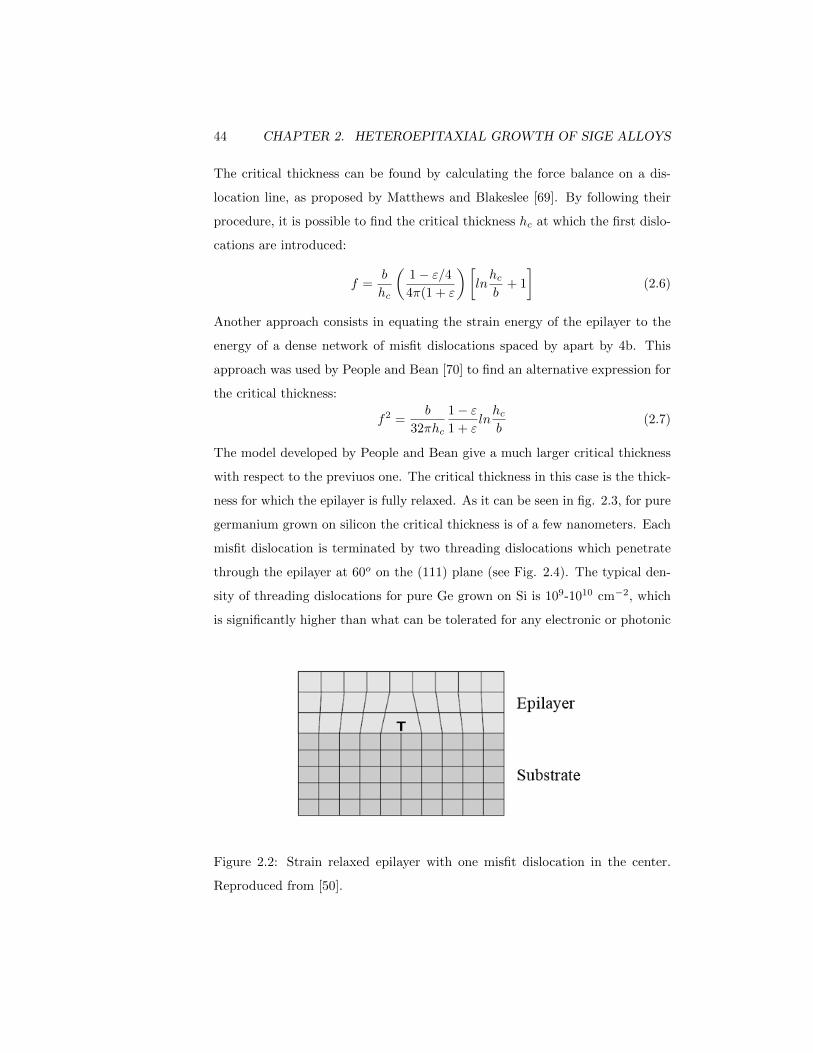
The critical thickness can be found by calculating the force balance on a dis-
location line, as proposed by Matthews and Blakeslee [69]. By following their
procedure, it is possible to find the critical thickness hc at which the first dislo-
cations are introduced:
f =b
hc
(1 − ε/4
4π(1 + ε
)[lnhcb
+ 1
](2.6)
Another approach consists in equating the strain energy of the epilayer to the
energy of a dense network of misfit dislocations spaced by apart by 4b. This
approach was used by People and Bean [70] to find an alternative expression for
the critical thickness:
f2 =b
32πhc
1 − ε
1 + εlnhcb
(2.7)
The model developed by People and Bean give a much larger critical thickness
with respect to the previuos one. The critical thickness in this case is the thick-
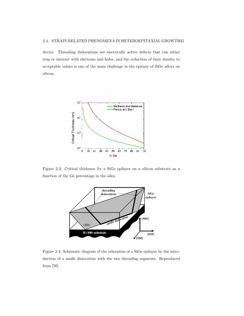
ness for which the epilayer is fully relaxed. As it can be seen in fig. 2.3, for pure
germanium grown on silicon the critical thickness is of a few nanometers. Each
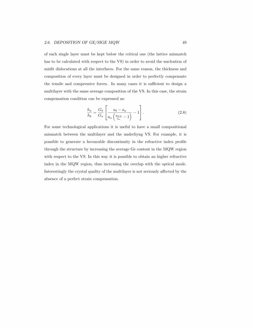
misfit dislocation is terminated by two threading dislocations which penetrate
through the epilayer at 60o on the (111) plane (see Fig. 2.4). The typical den-
sity of threading dislocations for pure Ge grown on Si is 109-1010 cm−2, which
is significantly higher than what can be tolerated for any electronic or photonic
Figure 2.2: Strain relaxed epilayer with one misfit dislocation in the center.
Reproduced from [50].
2.4. STRAIN RELATED PHENOMENA IN HETEROEPITAXIAL GROWTH45
device. Threading dislocations are electrically active defects that can either
trap or interact with electrons and holes, and the reduction of their density to
acceptable values is one of the main challenge in the epitaxy of SiGe alloys on
silicon.
Figure 2.3: Critical thickness for a SiGe epilayer on a silicon substrate as a
function of the Ge percentage in the alloy.
Figure 2.4: Schematic diagram of the relaxation of a SiGe epilayer by the intro-
duction of a misfit dislocation with the two threading segments. Reproduced
from [50].

46 CHAPTER 2. HETEROEPITAXIAL GROWTH OF SIGE ALLOYS
2.5 Growth of pure Ge on Si
Usually the epitaxy of Ge on Si is performed in a two-step process. In the initial
growth step, a thin Ge seed with a thickness of 30-60 nm is deposited at very low
temperatures (320-360 oC) in order to supress the islanding due to the strain.
Then the chamber temperature is raised to 600-650 oC to achieve higher growth
rates and crystal quality. In a LEPECVD reactor this is not necessary because
the islanding is kinetically suppressed. The whole deposition is performed in a
single step at a temperature of 500oC. After the growth, in order to reduce the
threading dislocation density, thermal annealing cycles are performed between
800oC and 600oC. The thermal stress, which is produced by the change of
temperature between the high and low temperature steps, generates a force,
causing the dislocations to move. If two dislocations meet, they react and
annhilate each other. The effectiveness of this procedure is strongly influenced
by the thickness of the epilayer (see Fig. 2.5). As the thickness increases, the
probability that two dislocations can meet and annhilate is strongly increased.
Figure 2.5: Experimentally measured threading dislocation density as a function
of the epilayer thickness.

2.6. DEPOSITION OF GE/SIGE MQW 47
2.6 Deposition of Ge/SiGe MQW
From the technolgical point of view, the deposition of Ge-rich Ge/SiGe MQW is
quite complicated. In order to obtain sharp interfaces between the Ge wells and
the SiGe barrier, the growth is performed at low temperature, typically between
425oC and 475oC. The low growth temperature ensures a limited interdiffusion
between the layers. Moreover the deposition is usually performed at low or
intermediate rate to have a good control on the thickness. The to main problems,
discussed in the next subsections, are the design of the virtual substrate and
the strain compensation in the MQW stack.
2.6.1 Virtual substrates
The design and optimization of the virtual substrate is extremely important,
because it influences significantly the structural and optical properties of the
MQW stack. The Ge content in the virtual substrate (VS) sets the lattice
parameter and the strain states for both the wells and the barriers. More-
over, since the VS is designed in order to have the same Ge content of the
MQW stack, the threading dislocation density of the VS is replicated in the
MQW stack. From the structural point of view, the main requirements are
a low threading dislocation density, a smooth surface and the full relaxation
of the VS. Also the thickness is an important design parameter. Considering
that the Ge/SiGe structure is meant to be used as an optical modulator, a low
thickness is preferred since it facilitates the integration with silicon waveguides.
The simpest way to deposit a fully relaxed Ge-rich VS is to grow a SiGe layer
directly on silicon, followed by some thermal annealing cycles in order to re-
duce the TDD. Unfortunately the annealing procedure is much less effective in
SiGe than in Ge. Alloy disorder inhibits dislocation gliding, thus reducing the
probability that threading dislocations can meet and annhilate. Moreover, the
annealing procedure is known to enhance the surface roughness of SiGe layers.
Nevertheless many efforts have been made in order to optimize the ”simple”
SiGe buffer layer because of the low thickness. Miller et al. [43] used a double

48 CHAPTER 2. HETEROEPITAXIAL GROWTH OF SIGE ALLOYS
step deposition followed by annealing. The ”simple” SiGe buffer can also be
deposited on a patterned SOI substrate to obtain selective area growth. This
technique was successfully employed with pure Ge grown on Si to reduce the
TDD through the aspect ratio trapping [71], and recently it was extended to
SiGe grown on SOI substrate by the group of Miller [72]. Another approach
to obtain an high quality SiGe VS is the deposition of the so called ”graded
buffer”. In a graded buffer, the Ge content is lineraly increased from 0% to the
required value, with a low grading rate which is usually kept below 10%/µm,
while the growth temperature is linearly decreased from 740 to 500 according
to the alloy composition. This technique was firstly introduced by Luryi et al
[73] and deeply studied by Fitzgerald [74]. By grading the concentration of Ge
in the alloy, the strain of each epilayer is low, thus the threading dislocations
coming from the initial layers can be used to relax the strain in the successive
layers. The nucleation of new misfit dislocations is supressed by this mecha-
nism, and thrading dislocation density as low as 10−6 cm−2 can be obtained
for a final Ge concentration around 90%. The major drawback is that the final
thickness of the buffer layer exceeds 10 µm, thus the graded buffer technique
cannot be considered for CMOS integration. Another possibility is the deposi-
tion of a reverse graded buffer. In this approach, a pure Ge layer, usually 1µm
thick is deposited and annealed, followed by the deposition of a SiGe layer with
a Ge concentration linearly decreasing from 100% to the desired value. This
technique was firstly proposed and studied by Shah [75]. The authors reported
a TDDs comparable to those obtainable with the graded buffer technique, with
a total thickness of the VS of only 2.8 µm. All the MQW samples described in
this thesis were grown by the graded buffer technique.
2.6.2 Strain compensation in multilayers
For the growth of strained multilayers such as multiple quantum wells, the strain
management is a critical point. In order to obtain a multilayered structure with
an high crystal quality, two requirements have to be fulfilled. The thickness
2.6. DEPOSITION OF GE/SIGE MQW 49
of each single layer must be kept below the critical one (the lattice mismatch
has to be calculated with respect to the VS) in order to avoid the nucleation of
misfit dislocations at all the interfaces. For the same reason, the thickness and
composition of every layer must be designed in order to perfectly compensate
the tensile and compressive forces. In many cases it is sufficient to design a
multilayer with the same average composition of the VS. In this case, the strain
compensation condition can be expressed as:
hahb
=GbGa
ab − aa
aa
(aV S
aa− 1) − 1
. (2.8)
For some technological applications it is useful to have a small compositional
mismatch between the multilayer and the underliyng VS. For example, it is
possible to generate a favourable discontinuity in the refractive index profile
through the structure by increasing the average Ge content in the MQW region
with respect to the VS. In this way it is possible to obtain an higher refractive
index in the MQW region, thus increasing the overlap with the optical mode.
Interestingly the crystal quality of the multilayer is not seriously affected by the
absence of a perfect strain compensation.

50 CHAPTER 2. HETEROEPITAXIAL GROWTH OF SIGE ALLOYS

Chapter 3
Ge/SiGe MQW for silicon
photonics
3.1 Optical modulation at 1.3 µm
3.1.1 Introduction
Several optical fiber telecommunications systems work in the spectral window
around 1.3µm, which corresponds to zero dispersion in standard single mode
fibers. In particular some passive optical network architectures use 1.3µm radi-
ation for upstream signal[76]. Therefore it is highly desirable to fabricate optical
modulators operating at this wavelength. The first demonstration of modula-
tion at 1.3µm by exploting QCSE in Ge/SiGe MQW was made by Lever et
al.[77]by using Ge/Si0.4Ge0.6 MQW grown on a Si0.22Ge0.78 virtual substrate.
With this material system, the large compressive strain in the wells pushes
the HH1-cΓ1 transition at 1.3µm. In this section, our work on modulation
at 1.3µm is presented. In order to fabricate a QCSE modulator operating at
1.3µm, we have used Ge/Si0.35Ge0.65 MQW grown on a Si0.21Ge0.79 virtual sub-
strate. In this material system, the excitonic resonances are wider with respect
to Ge/Si0.15Ge0.85 MQW because of the enhanced Γ-∆ scattering. This problem
51
52 CHAPTER 3. GE/SIGE MQW FOR SILICON PHOTONICS
will be analyzed and discussed.
3.1.2 Sample growth and charachterization
The sample was grown by LEPECVD on a 4 inch p-Si(001) substrate with
a resistivity in the range of 1-10 Ωcm. Before the heteroepitaxial growth, the
native oxide was removed by dipping the substrate in a hydrofluoric acid solution
(HF:H2O 1:10) for 30 s. The first part of the structure is made by an 11 µm
thick Si1−yGey graded buffer, deposited at a rate of 5-10 nm/s, in which the
Ge concentration y is linearly increased from 0% to 79% with a grading rate of
7%/µm. The top part of the graded buffer consists in a 2 µm Si0.21Ge0.79 layer
forming a fully relaxed virtual substrate. A 500 nm boron-doped Si0.21Ge0.79
layer was deposited to form the p-type contact region, followed by a 50 nm thick
Si0.21Ge0.79 spacer. The MQW structure is made of 20 periods of 8 nm thick Ge
QWs and 12 nm thick Si0.35Ge0.65 barriers grown at 475C at a rate of 1 nm/s.
Finally a 50 nm Si0.21Ge0.79 spacer and 200 nm phosphorus doped Si0.21Ge0.79
layer were deposited. A cross section of the structure is shown in fig. 3.1. Layer
compositions, thicknesses and strain states were measured by high-resolution X-
ray diffraction (HR-XRD) reciprocal space mapping (RSM) about the (004) and
(224) reflections using a PANalytical X’Pert PRO MRD diffractometer. Out-of-
plane and in-plane lattice parameters, a⊥ and a‖, were measured for the virtual
substrate peak and the superlattice satellites. Ge content and strain state were
obtained by using the known lattice parameters for relaxed SiGe alloys [79] and
interpolated elastic constants of Si and Ge [80]. The final composition of the VS
was found to be 79.9% with an in-plane strain of 0.05%). The in-plane lattice
parameter of the MQW stack is 0.5611 nm, the same as that of the virtual
substrate, meaning that the MQW stack is coherently matched to the virtual
substrate. Diffraction peaks from the VS and MQW structure are broadened
perpendicular to the relaxation line due to mosaicity in the virtual substrate.
The reciprocal space maps are shown in fig. 3.2. The lattice parameters and
the alloy concentrations extracted from the HR-XRD measurements have been

3.1. OPTICAL MODULATION AT 1.3 µM 53
Figure 3.1: Schematic cross section of the sample with detailed growth steps.
Figure 3.2: Reciprocal space maps of the sample about the 004 (a) and the 224
(b) reflections.

54 CHAPTER 3. GE/SIGE MQW FOR SILICON PHOTONICS
Figure 3.3: Simulated band-structure of the sample.
used to model the band structure of the sample through the NextNano software.
The high in-plane compressive strain in the well (0.6 %) pushes the HH1-cΓ1
transition at 0.965 eV, which corresponds to a wavelength of 1285 nm. In Fig
3.3 the simulated band structure and squared wavefunctions are reported.
3.1.3 Photocurrent Measurements
After the growth, the sample was processed into a square p-i-n diode (100 µm
x 114 µm) by UV lithography and dry etching. Metal contacts were formed
evaporating 10 nm of Cr followed by 300 nm of Au. Photocurrent measurements
were performed at room temperature in a surface illuminated configuration.
Randomly polarized light was shined by a tunable laser perpendicular to the
QW plane. The spectrum was recorded from 1.25 µm to 1.35 µm with a 1 nm
resolution, and the power of the laser was 0.5 mW. A chopper and a lock-in
amplifier were used to modulate the light intensity at 0.5 kHz and to collect
the photocurrent. The photocurrent spectra are reported in Fig. 3.4. A clear
exciton peak is visible at 1277 nm, in good agreement with the calculations. The
HWHM is approximately 12 meV, slightly larger than the 7 meV obtained for
Ge/Si0.15Ge0.85 MQW on Si0.1Ge0.9 VS[83]. The larger HWHM of the exciton
peak observed in the considered heterostructure is due a reduction of the Γ valley

3.1. OPTICAL MODULATION AT 1.3 µM 55
Figure 3.4: Photocurrent spectra.
lifetime resulting by the Γ-∆ intervalley scattering. This scattering channel
is not active in standard strain balanced Ge/Si0.15Ge0.85 MQW, where the Γ
valley lifetime is set only by the Γ-L intervalley scattering. This phenomenon
will be discussed in detail in the next section. As the applied electric field is
increased, the two main features of QCSE are observed. The absorption peak
shifts towards longer wavelengths following with a quadratic dependendece over
the electric field, and the exciton gradually broadens.
3.1.4 The role of Γ-∆ scattering
In this section, following the work of Lever et al. [84], the role of Γ-∆ scattering
on the Γ valley lifetime is analyzed and discussed. The scattering lifetime is a
very important parameter to be considered for QCSE based modulators, because
it sets the broadening of the excitonic peaks, and consequently the extinction
ratio. The first aspect to be considered is the significant splitting of the ∆ valley
caused by the large strain present in MQW grown on substrates with a large Si
fraction. As it can be seen in Fig. 3.5, there is a remarkable splitting between
the in-plane ∆4 and the out-of-plane ∆2 valleys with increasing Si fraction in the
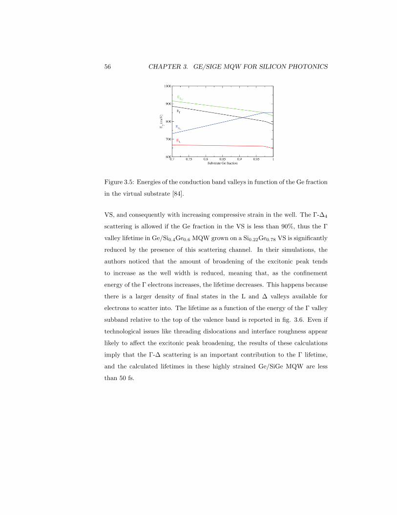
56 CHAPTER 3. GE/SIGE MQW FOR SILICON PHOTONICS
Figure 3.5: Energies of the conduction band valleys in function of the Ge fraction
in the virtual substrate [84].
VS, and consequently with increasing compressive strain in the well. The Γ-∆4
scattering is allowed if the Ge fraction in the VS is less than 90%, thus the Γ
valley lifetime in Ge/Si0.4Ge0.6 MQW grown on a Si0.22Ge0.78 VS is significantly
reduced by the presence of this scattering channel. In their simulations, the
authors noticed that the amount of broadening of the excitonic peak tends
to increase as the well width is reduced, meaning that, as the confinement
energy of the Γ electrons increases, the lifetime decreases. This happens because
there is a larger density of final states in the L and ∆ valleys available for
electrons to scatter into. The lifetime as a function of the energy of the Γ valley
subband relative to the top of the valence band is reported in fig. 3.6. Even if
technological issues like threading dislocations and interface roughness appear
likely to affect the excitonic peak broadening, the results of these calculations
imply that the Γ-∆ scattering is an important contribution to the Γ lifetime,
and the calculated lifetimes in these highly strained Ge/SiGe MQW are less
than 50 fs.

3.2. ELECTRO-REFRACTIVE EFFECT IN GE/SIGE MQW 57
Figure 3.6: Inverse Γ valley scattering lifetime components as a fuction of the
the energy of the Γ valley subband relative to the top of the valence band [84].
3.2 Electro-Refractive effect in Ge/SiGe MQW
3.2.1 Introduction
Intensity modulation is the simplest modulation format, namely on/off keying or
OOK. High level modulation formats such as QPSK are strongly needed in mod-
ern telecommunication systems and they are accesible only by the manipulation
of the phase of the light beam. In this section, our work on phase modulation
based on QCSE in Ge/SiGe QW is presented. As discussed in the first chapter,
QCSE causes strong variations in the absorption spectrum of a MQW based
device. These variations must be related to a change of the refractive index, as
stated by Kramers-Kronig relations:
∆n(λ) =λ2
2π2
∫∆α(λ
′)
λ2 − λ′2dx (3.1)
Large changes in the refractive index would make Ge/SiGe MQWs attractive
for the fabrication of electro-optic devices requiring phase shifters. For a given
combination of Ge/SiGe MQW and SiGe virtual substrate, the electro-refractive
(ER) effect is able to work at longer wavelengths with respect to those of the
electro-absorption, constituting a powerful approach to extend the operative
wavelengths of modulators based on this material system.
58 CHAPTER 3. GE/SIGE MQW FOR SILICON PHOTONICS
3.2.2 Sample growth and characterization
The structure was deposited on a 100 mm p-Si(001) substrate with a resistivity
of 1-10 Ωcm. Before heteroepitaxy, the native silicon doxide was removed by
dipping the substrate in aqueous hydrofluoric acid solution (HF:H2O 1:10) for
30 s. The first part of the structure is made by an 13 µm thick Si1yGey graded
buffer, deposited at a rate of 5-10 nm/s, in which the Ge concentration y is
linearly increased from 0% to 90% with a grading rate of 7%/µm and capped
with a 2 m Si0.1Ge0.9 layer forming a fully relaxed virtual substrate. The graded
buffer was grown in 180 steps. In each step the germanium concentration was
raised by 0.5% by increasing the GeH4 flow while keeping costant the flow
of SiH4. As the amount of process gases increases, the deposition rate also
increases. The grading rate was maintained constant by varying the time of
each step according to the depostion rate. The threading dislocation density
in the VS was 6× 106 cm−2 as measured by chemical defect etching. A 500
nm boron doped (1019 cm−3) Si0.1Ge0.9 layer was deposited to form the p-type
contact region, followed by a 50 nm Si0.1Ge0.9 spacer. The MQW structure
consists of 20 periods of 10 nm thick Ge QWs and 15 nm thick Si0.15Ge0.85
barriers grown at 475C at a rate of 1 nm/s. The individual layer thicknesses
were designed in order to compensate the compressive strain in the Ge well with
the tensile strain in the barrier. Finally a 50 nm Si0.1Ge0.9 layer spacer and 100
nm phosphorus doped ( 1019 cm−3) Si0.1Ge0.9 layer were deposited. A cross
section of the device showing detailed epitaxy steps is reported in Fig.3.7. As
for the previous sample, layer compositions and strain states were measured by
high-resolution X-ray diffraction (HR-XRD) reciprocal space mapping (RSM)
about the (004) and (224) reflections. The final composition of the VS was found
to be 92% with an in-plane strain of 0.087%). The in-plane lattice parameter
of the MQW stack is 0.5634 nm, the same as that of the virtual substrate,
meaning that the MQW stack is coherently matched to the virtual substrate.
The reciprocal space maps are shown in fig. 3.8.

3.2. ELECTRO-REFRACTIVE EFFECT IN GE/SIGE MQW 59
Figure 3.7: Schematic cross section of the sample with detailed growth steps.
Figure 3.8: Reciprocal space maps of the sample about the 004 (a) and the 224
(b) reflections.

60 CHAPTER 3. GE/SIGE MQW FOR SILICON PHOTONICS
3.2.3 Device processing
In order to investigate the electro-refractive effect in Ge/SiGe MQW, absorption
measurements were performed on 64 µm long, 100 µm wide planar waveguides.
The waveguides were processed by UV lithography and dry etching. The side-
wall roughness of the etched mesa was also smoothened by hydrogen peroxide
(H2O2) solution. A few tens of nanometers of silicon dioxide were deposited
by PECVD to serve as a passivation layer on the left and right walls of the
waveguide. To form metal contacts, 600 nm of Al were evaporated and lifted off
for both p and n layers. The top contact covers only part of the waveguide slab
to minimize absorption from the metal. As the waveguide length is 64 µm, a
deep etch of 90 µm was performed to bring the input fiber and output objective
to the input and output facets of the waveguides. A cross section of the device
is shown in Fig. 3.9.
Figure 3.9: Cross section of the device used for the characterization of the
electro-refractive effect. Reproduced from [85].

3.2. ELECTRO-REFRACTIVE EFFECT IN GE/SIGE MQW 61
3.2.4 Experimental charachterization of the ER effect
The absorption measurements were performed at room temperature with a spec-
tral resolution of 0.1 nm by using a tunable laser emitting light from 1390 to
1540 nm with a power of 1 mW. Light from the laser was butt coupled into the
planar waveguide by using a taper-lensed fiber, which was placed to inject light
in the waveguide region not covered by the top metal contact to reduce optical
losses. An objective was used to couple the output light into a photodiode. The
spectra were recorded only for TE polarized light. A scheme of the experimental
set-up used is shown in Fig. 3.10 and the absorption spectra of the device in for
different applied electric fields is shown in Fig. 3.11. After each measurement
at a given electric field, a measurement at 0V was done to check for the absence
of thermal induced shift. The current voltage characteristic of the device is
reported in the inset of Fig.3.11. The absorption edge is shifted from the 0.8
eV of bulk Ge due to both the confinement effect and the compressive strain in
the Ge well. Without bias voltage, an exciton peak related to the transitions
between the first heavy hole subband and the first electronic level in the con-
duction band at the point (HH1-cΓ1) is observed at 0.888 eV. By increasing the
applied electric field, two main characteristics of the QCSE are observed: the
Stark shift of the absorption spectra and the reduction of the exciton related ab-
Figure 3.10: Diagram of the experimental set-up used to perform absorption
measurements of the device.
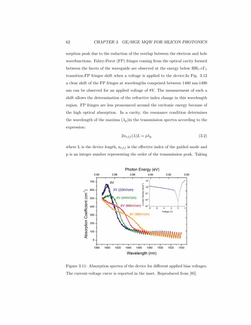
62 CHAPTER 3. GE/SIGE MQW FOR SILICON PHOTONICS
sorption peak due to the reduction of the overlap between the electron and hole
wavefunctions. Fabry-Perot (FP) fringes coming from the optical cavity formed
between the facets of the waveguide are observed at the energy below HH1-cΓ1
transition.FP fringes shift when a voltage is applied to the device.In Fig. 3.12
a clear shift of the FP fringes at wavelengths comprised between 1480 nm-1490
nm can be observed for an applied voltage of 8V. The measurement of such a
shift allows the determination of the refractive index change in this wavelength
region. FP fringes are less pronounced around the excitonic energy because of
the high optical absorption. In a cavity, the resonance condition determines
the wavelength of the maxima (λp)in the transmission spectra according to the
expression:
2neff (λ)L = pλp (3.2)
where L is the device length, neff is the effective index of the guided mode and
p is an integer number representing the order of the transmission peak. Taking
Figure 3.11: Absorption spectra of the device for different applied bias voltages.
The current-voltage curve is reported in the inset. Reproduced from [85]
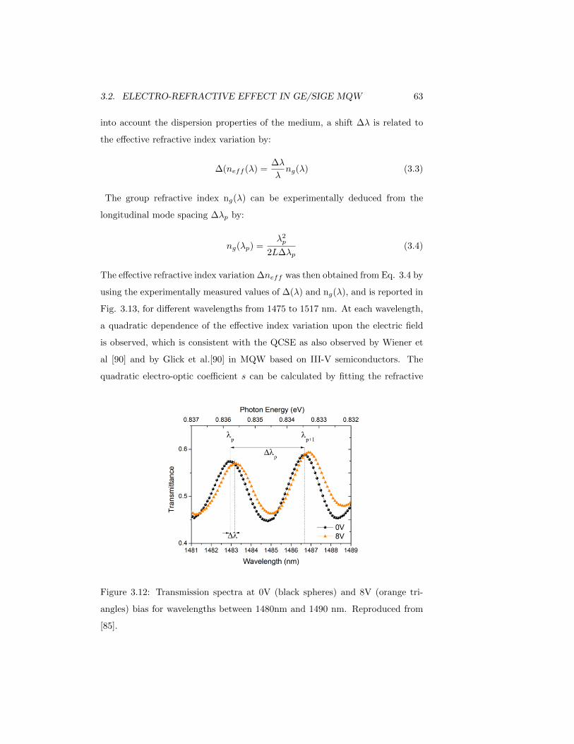
3.2. ELECTRO-REFRACTIVE EFFECT IN GE/SIGE MQW 63
into account the dispersion properties of the medium, a shift ∆λ is related to
the effective refractive index variation by:
∆(neff (λ) =∆λ
λng(λ) (3.3)
The group refractive index ng(λ) can be experimentally deduced from the
longitudinal mode spacing ∆λp by:
ng(λp) =λ2p
2L∆λp(3.4)
The effective refractive index variation ∆neff was then obtained from Eq. 3.4 by
using the experimentally measured values of ∆(λ) and ng(λ), and is reported in
Fig. 3.13, for different wavelengths from 1475 to 1517 nm. At each wavelength,
a quadratic dependence of the effective index variation upon the electric field
is observed, which is consistent with the QCSE as also observed by Wiener et
al [90] and by Glick et al.[90] in MQW based on III-V semiconductors. The
quadratic electro-optic coefficient s can be calculated by fitting the refractive
Figure 3.12: Transmission spectra at 0V (black spheres) and 8V (orange tri-
angles) bias for wavelengths between 1480nm and 1490 nm. Reproduced from
[85].
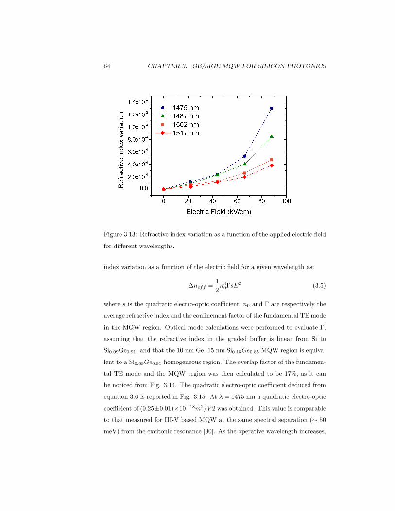
64 CHAPTER 3. GE/SIGE MQW FOR SILICON PHOTONICS
Figure 3.13: Refractive index variation as a function of the applied electric field
for different wavelengths.
index variation as a function of the electric field for a given wavelength as:
∆neff =1
2n3
0ΓsE2 (3.5)
where s is the quadratic electro-optic coefficient, n0 and Γ are respectively the
average refractive index and the confinement factor of the fundamental TE mode
in the MQW region. Optical mode calculations were performed to evaluate Γ,
assuming that the refractive index in the graded buffer is linear from Si to
Si0.09Ge0.91, and that the 10 nm Ge 15 nm Si0.15Ge0.85 MQW region is equiva-
lent to a Si0.09Ge0.91 homogeneous region. The overlap factor of the fundamen-
tal TE mode and the MQW region was then calculated to be 17%, as it can
be noticed from Fig. 3.14. The quadratic electro-optic coefficient deduced from
equation 3.6 is reported in Fig. 3.15. At λ = 1475 nm a quadratic electro-optic
coefficient of (0.25±0.01)×10−18m2/V 2 was obtained. This value is comparable
to that measured for III-V based MQW at the same spectral separation (∼ 50
meV) from the excitonic resonance [90]. As the operative wavelength increases,
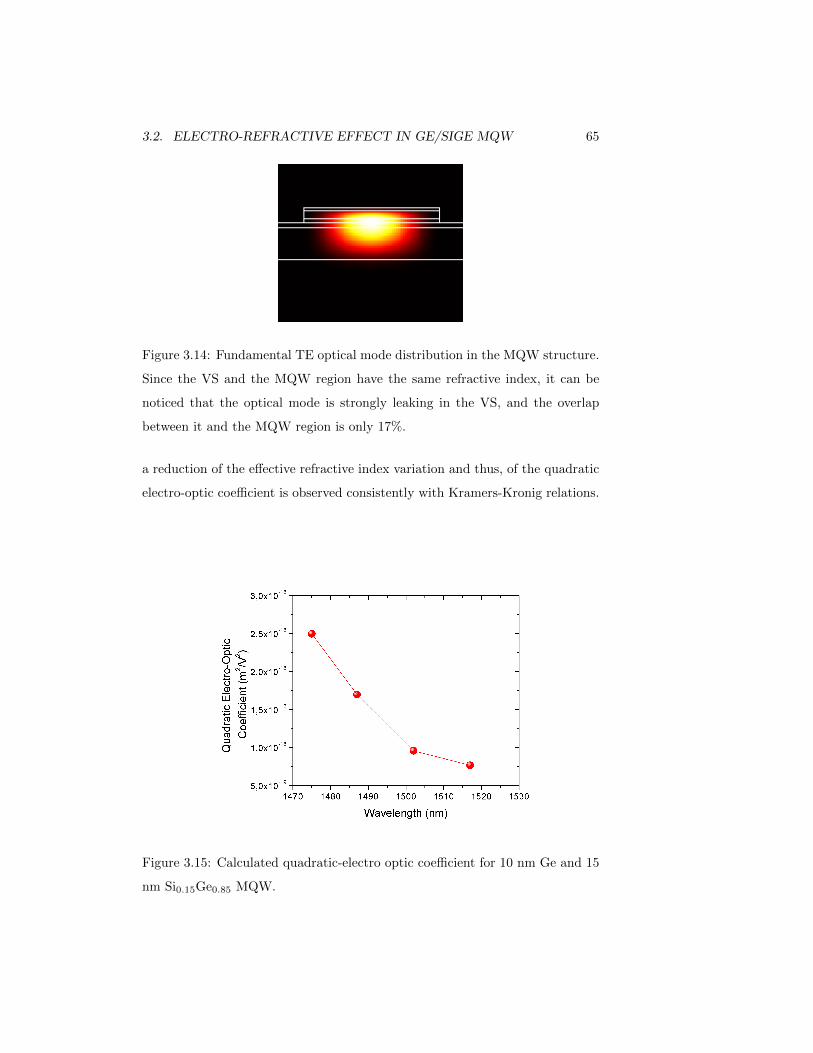
3.2. ELECTRO-REFRACTIVE EFFECT IN GE/SIGE MQW 65
Figure 3.14: Fundamental TE optical mode distribution in the MQW structure.
Since the VS and the MQW region have the same refractive index, it can be
noticed that the optical mode is strongly leaking in the VS, and the overlap
between it and the MQW region is only 17%.
a reduction of the effective refractive index variation and thus, of the quadratic
electro-optic coefficient is observed consistently with Kramers-Kronig relations.
Figure 3.15: Calculated quadratic-electro optic coefficient for 10 nm Ge and 15
nm Si0.15Ge0.85 MQW.

66 CHAPTER 3. GE/SIGE MQW FOR SILICON PHOTONICS
3.2.5 Evaluation of the device performance
In order to investigate the viability of a phase-shifter based on this device ar-
chitecture, the device lenght necessary to achieve a π phase shift was calculated
with the following formula:
Lπ =λ
2∆neff(3.6)
The results are reported in Fig. 3.16. For λ = 1475 nm, the Lπ is 570 µm for
an applied electric field of 8.8× 10⁴ V/cm with a corresponding VπLπ figure
of merit of 0.46 Vcm. This value is comparable with the published values of
Mach Zehnder modulators based on GaAs/AlGaAs MQW (0.55 Vcm) [86], and
competitive with those of silicon (3.3 Vcm) [87]. It is worth noting that residual
absorption of 50 cm−1 100 cm−1 is observed in the spectral region above the
excitonic resonance. However, as shown in ref. 88, the indirect-gap related
absorption of the Ge/SiGe MQW at 50 meV from the excitonic resonance is
expected to be lower than what we measured in this work. For this reason,
the residual absorption has been mainly attributed to the indirect interband
transitions in the Ge-rich part of the VS, and may be reduced by increasing of
the overlap factor of the guided mode with the MQW region.
Figure 3.16: Calculated Lπ for the device. This parameter represent the device
lenght necessary to achieve a π phase shift for a given applied voltage.
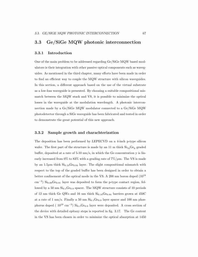
3.3. GE/SIGE MQW PHOTONIC INTERCONNECTION 67
3.3 Ge/SiGe MQW photonic interconnection
3.3.1 Introduction
One of the main problem to be addressed regarding Ge/SiGe MQW based mod-
ulators is their integration with other passive optical components such as waveg-
uides. As mentioned in the third chapter, many efforts have been made in order
to find an efficient way to couple the MQW structure with silicon waveguides.
In this section, a different approach based on the use of the virtual substrate
as a low-loss waveguide is presented. By choosing a suitable compositional mis-
match between the MQW stack and VS, it is possible to minimize the optical
losses in the waveguide at the modulation wavelength. A photonic intercon-
nection made by a Ge/SiGe MQW modulator connected to a Ge/SiGe MQW
photodetector through a SiGe waveguide has been fabricated and tested in order
to demonstrate the great potential of this new approach.
3.3.2 Sample growth and charachterization
The deposition has been performed by LEPECVD on a 4-inch p-type silicon
wafer. The first part of the structure is made by an 11 m thick Si1yGey graded
buffer, deposited at a rate of 5-10 nm/s, in which the Ge concentration y is lin-
early increased from 0% to 83% with a grading rate of 7%/µm. The VS is made
by an 1.5µm thick Si0.16Ge0.84 layer. The slight compositional mismatch with
respect to the top of the graded buffer has been designed in order to obtain a
better confinement of the optical mode in the VS. A 200 nm boron doped (1019
cm−3) Si0.09Ge0.91 layer was deposited to form the p-type contact region, fol-
lowed by a 50 nm Si0.1Ge0.9 spacer. The MQW structure consists of 10 periods
of 12 nm thick Ge QWs and 16 nm thick Si0.16Ge0.84 barriers grown at 450C
at a rate of 1 nm/s. Finally a 50 nm Si0.1Ge0.9 layer spacer and 100 nm phos-
phorus doped ( 1019 cm−3) Si0.1Ge0.9 layer were deposited. A cross section of
the device with detailed epitaxy steps is reported in fig. 3.17. The Ge content
in the VS has been chosen in order to minimize the optical absorption at 1450

68 CHAPTER 3. GE/SIGE MQW FOR SILICON PHOTONICS
Figure 3.17: Cross section of the sample used to realize the optical interconnec-
tion.
Figure 3.18: Reciprocal space maps of the sample about the 004 (a) and the
224 (b) reflections.
3.3. GE/SIGE MQW PHOTONIC INTERCONNECTION 69
nm[91], which is the working wavelength of the MQW modulator according to
the simulations. At the same time, the compositional mismatch between the
VS and the MQW stack is low enough to avoid the introduction of new misfit
dislocations at the interface. The structural properties of the sample have been
determined by HR-XRD (See fig. 3.18). The VS and the 0th order superlattice
peak do not share the same q|| because of the compositional mismatch. Never-
theless, the sharp satellite peaks indicate a good crystal quality for the MQW
stack.
3.3.3 Device processing and Measurements
Three differnt devices have been fabricated: (i) Si0.16Ge0.84 waveguides with
different lenghts; (ii) a Ge/Si0.16Ge0.84 MQW p-i-n diode and (iii) a photonic
interconnetion made by a Ge/Si0.16Ge0.84 MQW modulator and photodetector
connected by a Si0.16Ge0.84 waveguide. All the devices have been patterned by
UV lithography and dry etching. The photodiode and the modulator were also
passivated with Si3N4 and SiO2 deposited by PECVD and metallized to create
electrical contacts.
Si0.16Ge0.84 waveguides
The waveguides have been fabricated and tested in order to determine the optical
losses. Rib waveguides 2 µm wide and 1.5 µm thick were processed with lenghts
of 750, 1250, 1750, 2250, and 2750 µm (see fig. 3.19). As shown in fig. 3.20,
optical losses of 5dB/cm and of 2dB/cm can be obtained at wavelengths longer
than 1410 and 1440 nm respectively. In order to determine the losses of the
waveguides, optical transmission measurements have been performed on each
waveguide in the spectral range from 1340 to 1540 nm.
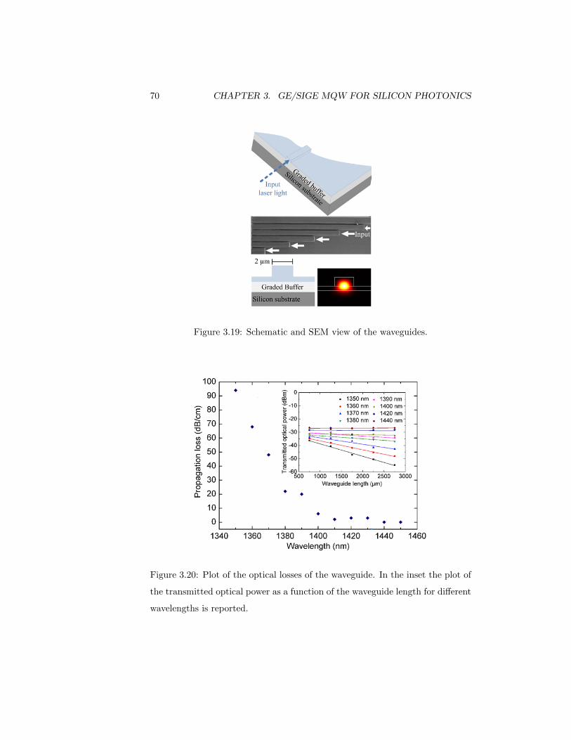
70 CHAPTER 3. GE/SIGE MQW FOR SILICON PHOTONICS
Figure 3.19: Schematic and SEM view of the waveguides.
Figure 3.20: Plot of the optical losses of the waveguide. In the inset the plot of
the transmitted optical power as a function of the waveguide length for different
wavelengths is reported.
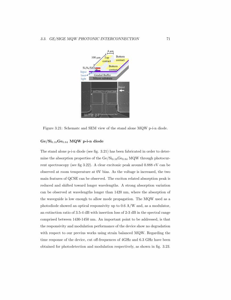
3.3. GE/SIGE MQW PHOTONIC INTERCONNECTION 71
Figure 3.21: Schematc and SEM view of the stand alone MQW p-i-n diode.
Ge/Si0.16Ge0.84 MQW p-i-n diode
The stand alone p-i-n diode (see fig. 3.21) has been fabricated in order to deter-
mine the absorption properties of the Ge/Si0.16Ge0.84 MQW through photocur-
rent spectroscopy (see fig 3.22). A clear excitonic peak around 0.888 eV can be
observed at room temperature at 0V bias. As the voltage is increased, the two
main features of QCSE can be observed. The exciton related absorption peak is
reduced and shifted toward longer wavelengths. A strong absorption variation
can be observed at wavelengths longer than 1420 nm, where the absorption of
the waveguide is low enough to allow mode propagation. The MQW used as a
photodiode showed an optical responsivity up to 0.6 A/W and, as a modulator,
an extinction ratio of 3.5-4 dB with insertion loss of 2-3 dB in the spectral range
comprised between 1430-1450 nm. An important point to be addressed, is that
the responsivity and modulation performance of the device show no degradation
with respect to our previus works using strain balanced MQW. Regarding the
time response of the device, cut off-frequences of 4GHz and 6.3 GHz have been
obtained for photodetection and modulation respectively, as shown in fig. 3.23.

72 CHAPTER 3. GE/SIGE MQW FOR SILICON PHOTONICS
Figure 3.22: Absorption spectra of the stand alone MQW p-i-n diode with
different applied voltages.
Figure 3.23: Time response of the MQW device for detection (a) and modulation
(b).

3.3. GE/SIGE MQW PHOTONIC INTERCONNECTION 73
Figure 3.24: Scheme and SEM view of the processed photonic link
Photonic Interconnection
The scheme of the photonic inteconnection is reported in fig. 3.24. The IV
characteristics of both the modulator and the detector are reported in Fig.
3.25(a) when the same bias voltage is applied to the devices. The measurements
have been performed by using a tunable laser with an output power of 3 mW at
a wavelength of 1440 nm. The photocurrent in the photodetector is lower only
by a factor 3 with respect to that of the modulator, and both devices have the
same size. The optical insertion loss is less than 5 dB, thus the performances of
the photonic interconnect are even better than that reported for III-V devices
bonded on silicon [92]. In Fig. 3.25(b) are reported the IV characterstic of the
photodetector for different bias voltages applied to the modulator at 1440 nm.
5 and 10 µA between the ”0” and the ”1” logic levels have been obtained by
using 1V and 3V voltage swing at the modulator, respectively. The photodector,
biased at -1V have shown a dark current of 10 nA, thus the shot noise is only
2.5 pA/Hz−1/2. The photonic interconnect thus has a very promising potential
for low bit error rate data transmission.

74 CHAPTER 3. GE/SIGE MQW FOR SILICON PHOTONICS
Figure 3.25: IV characteristics of the fabricated photonic interconnect (a) and
photocurrents at the photodetector with different reverse bias voltages at the
optical modulator.

Chapter 4
Hyghly strained Ge
micro-bridges
4.1 Introduction
Tensile strain is an extremely powerful tool to engineer the Ge bandstructure in
order to turn this element into an efficient light emitter. As mentioned previ-
ously, also n-type doping can be employed in order to achieve such a target, but
it is associated with several drawback such as the enhancement of non radiative
recombination and free carrier absorption. For this reason the research toward
an efficient Ge laser is now focused on the enhancement of tensile strain through
post growth approaches. In this chapter our work carried out with the team of
Dr. Hans Sigg of the PSI and of Prof. Jerome Faist and Ralph Spolenak of th
ETH, is presented. Our approach is based on a top-down fabrication method
developed to realize highly uniaxially strained Ge microbridges on Si and on
SOI. In this first work, an undoped sample was used in order to investigate the
effect of an high level of tensile strain on the band structure of germanium.
75
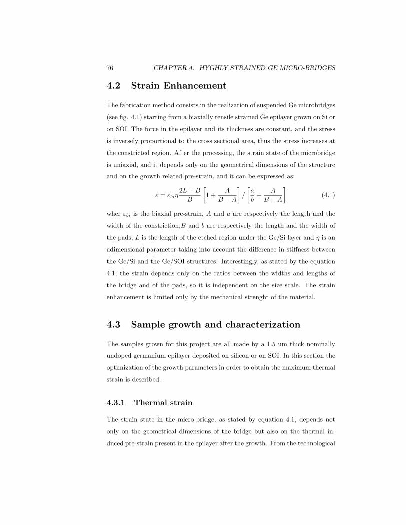
76 CHAPTER 4. HYGHLY STRAINED GE MICRO-BRIDGES
4.2 Strain Enhancement
The fabrication method consists in the realization of suspended Ge microbridges
(see fig. 4.1) starting from a biaxially tensile strained Ge epilayer grown on Si or
on SOI. The force in the epilayer and its thickness are constant, and the stress
is inversely proportional to the cross sectional area, thus the stress increases at
the constricted region. After the processing, the strain state of the microbridge
is uniaxial, and it depends only on the geometrical dimensions of the structure
and on the growth related pre-strain, and it can be expressed as:
ε = εbiη2L+B
B
[1 +
A
B −A
]/
[a
b+
A
B −A
](4.1)
wher εbi is the biaxial pre-strain, A and a are respectively the length and the
width of the constriction,B and b are respectively the length and the width of
the pads, L is the length of the etched region under the Ge/Si layer and η is an
adimensional parameter taking into account the difference in stiffness between
the Ge/Si and the Ge/SOI structures. Interestingly, as stated by the equation
4.1, the strain depends only on the ratios between the widths and lengths of
the bridge and of the pads, so it is independent on the size scale. The strain
enhancement is limited only by the mechanical strenght of the material.
4.3 Sample growth and characterization
The samples grown for this project are all made by a 1.5 um thick nominally
undoped germanium epilayer deposited on silicon or on SOI. In this section the
optimization of the growth parameters in order to obtain the maximum thermal
strain is described.
4.3.1 Thermal strain
The strain state in the micro-bridge, as stated by equation 4.1, depends not
only on the geometrical dimensions of the bridge but also on the thermal in-
duced pre-strain present in the epilayer after the growth. From the technological

4.3. SAMPLE GROWTH AND CHARACTERIZATION 77
Figure 4.1: SEM view of a microbridge. In the figure the main geometrical
parameters are indicated.
point of view, the maximimum thermal strain achievable depends on the maxi-
mum temperature reached during the annealing procedure and on the cool-down
rapidity. A series of four samples were grown in order to optimize the anneal-
ing procedure. All the samples have been grown by LEPECVD on 4-inch Si
substrates. They consist in a 1.5µm thick nominally undoped germanium epi-
layer grown at 500o at intermediate rate. The maximum substrate temperature
achievable in the LEPECVD reactor is around 800oC. For this reason, in order
to maximize the thermal strain, we have used an external rapid thermal anneal-
ing tool to perform the annealing procedure. The five samples were annealed
at different temperatures in a forming gas atmosphere. After the annealing,
the strain state was charachterized by HR-XRD (see fig. 4.2) and the surface
roughness was measured by atomic force microscopy (see fig. 4.3). A trade-off
between the surface quality and the thermal strain is expected, thus the aim
of this experiment was to find the optimal annealing temperature. The results
are summarized in tab 4.1. From the XRD analysis, it can be noticed the the

78 CHAPTER 4. HYGHLY STRAINED GE MICRO-BRIDGES
Figure 4.2: HR-XRD ω-2θ scans of the four samples used for the optimization of
the annealing procedure. The annealing temperatures are (a) 750oC, (b) 800oC,
(c) 850oC, (d) 900oC.

4.3. SAMPLE GROWTH AND CHARACTERIZATION 79
Figure 4.3: AFM scans of the four samples used for the optimization of the
annealing procedure. The annealing temperatures are (a) 750oC, (b) 800oC, (c)
850oC, (d) 900oC. The area of the AFM scans is 30µm × 30µm.
80 CHAPTER 4. HYGHLY STRAINED GE MICRO-BRIDGES
Sample Annealing Temperature (oC) Tensile Strain (%) surface roughness (nm)
A 750 0.19 0.92
B 800 0.21 1.56
C 850 0.22 2.15
D 900 0.22 2.52
Table 4.1: Results of the annealing procedure optimization
thermal tensile strain present in the epilayer saturates at 0.22%, reached for an
annealing temperature of 850 oC. Moreover, the AFM scans show the presence
of holes on the surface for the sample D, annealed at 900oC. Thus the optimal
annealing temperature was found to be 850oC.
4.4 Fabrication of the micro-bridge
The sample used for this work was grown by LEPECVD on an SOI substrate.
The substrate have a 1µm thick SiO2 BOX layer and a 340 nm thick Si device
layer. The sample consists in an 1.5 µm thick nominally undoped germanium
layer grown at approximately 1 nm/s at a temperature of 500oC. After the
growth, thermal annealing cycles were performed in order to reduce the thread-
ing dislocation density. A schematic cross section of the sample is shown in fig.
4.5. The sample was then characterized by HR-XRD. The biaxial strain was
0.18 %, which is slightly lower with respect to what obtained with silicon sub-
strates because of the different stiffness of the SOI. The reciprocal space maps
are shown in fig 4.6. After the growth, the sample was covered by 60 nm of Cr.
The micro-bridge structures were then patterned using PMMA and standard
electron beam lithography. After dry etching of the Cr mask, the Ge and Si
layers were etched down to the BOX with SF6-based reactive ion etching. The
final structures were released from the substrate by hydrofluoric acid. A scheme
of the main fabrication steps is shown in Fig. 4.7.
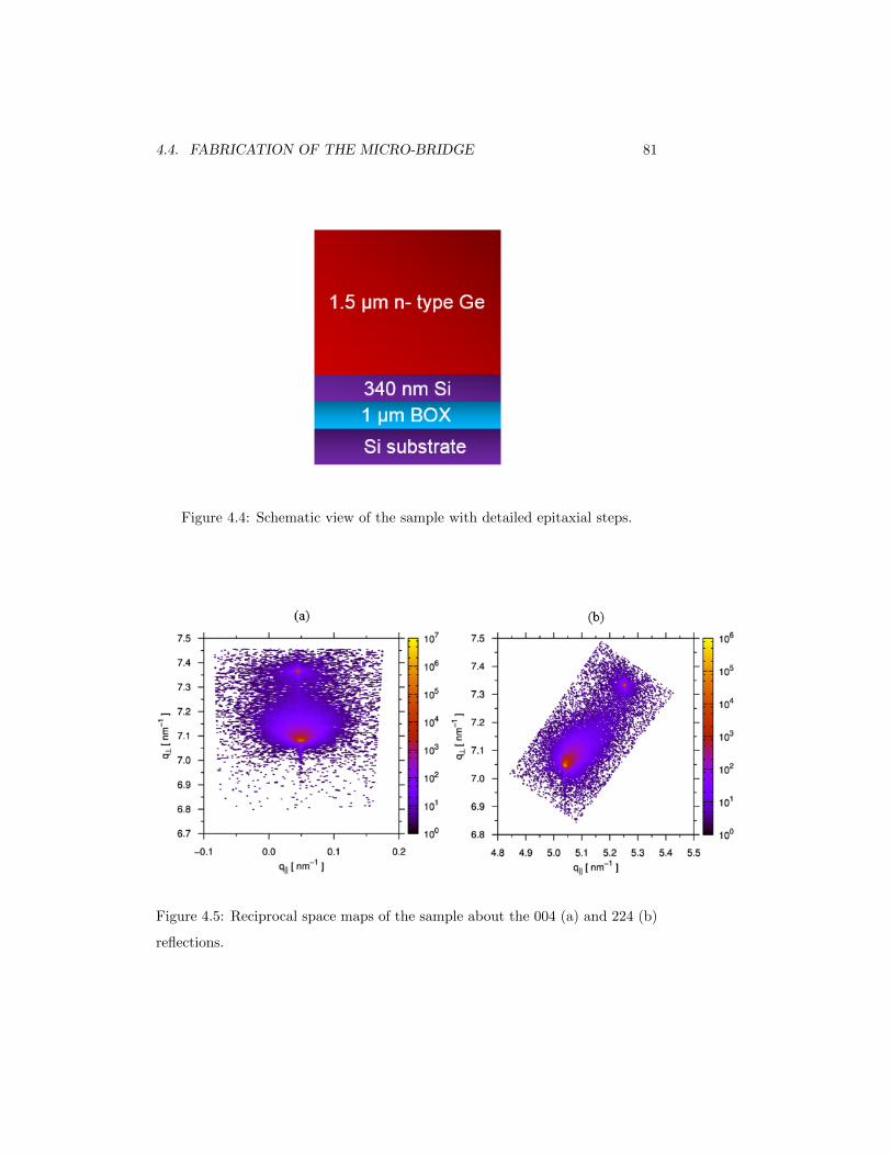
4.4. FABRICATION OF THE MICRO-BRIDGE 81
Figure 4.4: Schematic view of the sample with detailed epitaxial steps.
Figure 4.5: Reciprocal space maps of the sample about the 004 (a) and 224 (b)
reflections.

82 CHAPTER 4. HYGHLY STRAINED GE MICRO-BRIDGES
Figure 4.6: Schematic view of the main steps of the micro-bridge fabrication
process [91].
4.5 Raman measurements
The strain state of the micro-bridge was measured by Raman spectroscopy. The
spectra were recorded in different positions on the suspended Ge/SOI structure,
and the results are plotted in fig 4.8. The spectrum for bulk unstrained germa-
nium (black dashed curve) is plotted as a reference. The peak measured far from
the bridge structure (red peak) is shifted by 0.65 cm−1 with respect to the bulk,
corresponding to a biaxial strain of 0.18%. The peak related to the constriction
(green curve) is shifted by about -4.8% with respect to the bulk reference. This
value corresponds to a longitudinal strain εxx of 3.1%. Interestingly, the peak
measured on the pad (blue curve) is very close to the unstrained bulk reference,
meaning that the strain in the constriction is accumulated at the expense of
relaxation in the pads.
4.6 Photoluminescence measurements
In Fig. 4.9 are reported the micro-photoluminescence spectra recorded at room
temperature in different micro-bridge structures with different strain levels. The
excitation power was 4.5 mW from a laser source operating in continuous wave
at a wavelength of 532 nm. The laser spot size was set to a diameter of 0.8 µm.
The oscillations in the spectra are attributed to Fabry-Perot resonances of the
suspended structures, as demonstrated by the reflection spectrum shown at the
bottom of fig. 4.9. Unfortunately, the identification of the contribution from
several possible radiative transitions from L and Γ conduction band minima to

4.6. PHOTOLUMINESCENCE MEASUREMENTS 83
Figure 4.7: Normalized Raman spectra (a) taken at position indicated by
coloured triangles in (b). Reproduced from[91].
the valence band are difficult to identify due to the presence of Fabry-Perot
resonances. Nevertheless, a red-shift and an increase of the intensity of the
photoluminescence peak with increasing longitudinal strain is clearly visible.
For the maximum longitudinal strain (3.1%) the photoluminescence peak is
shifted of 210 meV and its intensity is increased by a factor 25 with respect to
the bulk reference. This is a clear indication of reduced bandgap energy as well
as a decreased energy separation between the L and Γ minima.
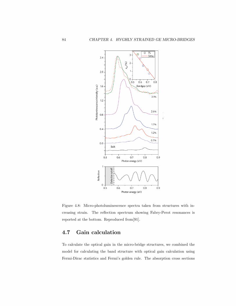
84 CHAPTER 4. HYGHLY STRAINED GE MICRO-BRIDGES
Figure 4.8: Micro-photoluminescence spectra taken from structures with in-
creasing strain. The reflection spectrum showing Fabry-Perot resonances is
reported at the bottom. Reproduced from[91].
4.7 Gain calculation
To calculate the optical gain in the micro-bridge structures, we combined the
model for calculating the band structure with optical gain calculation using
Fermi-Dirac statistics and Fermi’s golden rule. The absorption cross sections

4.7. GAIN CALCULATION 85
Figure 4.9: Gain simulation for 3.1% strained Ge structures doped and undoped.
Reproduced from[91].
of the intraband absorption in the valence band, the main loss channel, were
extracted from [64]. In fig. 4.10 is reported the energy-dependent absorption of
an undoped and an n-doped (1019 cm−3 Ge epilayer with 3.1% uniaxial strain
at an injection density of 3 × 1019 cm−3. We find that the material gain exceeds
the loss for the doped sample, but for an undoped sample as the investigated
one, only the transparency can be reached.

86 CHAPTER 4. HYGHLY STRAINED GE MICRO-BRIDGES

Chapter 5
Carrier lifetime study in
Ge-on-Si epilayers
5.1 Introduction
In the route toward the realization of an efficient Ge-on-Si laser, several mate-
rial parameters, such as carrier induced optical loss, carrier lifetimes and non
radiative recombination have to be taken into account. The properties of doped
Ge-on-Si epilayers can deviate substantially from the properties known for in-
trinsic bulk Ge, due to the defective layer formed at the Ge/Si interface and to
the doping. In this chapter, a study on excess carrier lifetime in Ge-on-Si epi-
layers is presented. Pump-probe transmission spectroscopy was used to extract
the excess carrier lifetime on differently prepared Ge-on-Si samples. The exper-
iment was designed in order to highlight the impact of the growth parameters,
such as doping and post growth annealing, on the lifetime. The transmission
measurements were performed at the X01DC beamline of the Swiss light source
using the broadband synchrotron radiation as the probe pulse. Pump pulses
of 100 ps were delivered by a Nd:YAG laser at a wavelength of 1064 nm. Due
to multiple interferences within the layered stack, the transmission spectra are
87

88 CHAPTER 5. CARRIER LIFETIME STUDY IN GE-ON-SI EPILAYERS
modulated by Fabry-Perot oscillations. The photoexcited carriers change the
refractive index of the material, leading to a phase shift of the oscillations. By
follwing the temporal dependence of this phase shift for increasing pump-probe
delay time, it is possible to extract the carrier lifetime.
5.2 N-type doping calibration
In order to highlight the impact of n-type doping on the carrier lifetime, a
calibration of the n-doping was performed. The doping is obtained in-situ, by
adding PH3 to the process gas mixture during the growth. The concentration
and uniformity of dopants into the epilayer depends on many growth parameters,
such as the ratio between the flows of PH3 and GeH4, the growth temperature,
the intensity of the plasma and the annealing procedure. In this section the
calibration and optimization of n-type doping is presented, as well as the role
of the aforementioned growth parameters.
5.2.1 PH3/GeH4 ratio
In order to determine the relation between the active donor concentration and
the ratio between the flows of PH3 and GeH4, seven samples have been grown.
All the samples consist in 1 µm thick Ge epilayer grown at 500oC at intermediate
rate on intrinsic SOI substrates. The GeH4 flow has been kept to 20 sccm for
all the samples, while the PH3 flow has been varied for every sample. Since
the growth rate is dependent on the amount of PH3 in the gas mixture, the
thickness of each sample has been measured by SEM. After the growth, the
samples have been processed by UV lithography and dry etching in order to
obtain six-terminals Hall bars. Finally Ti/Au contacts have been deposited by
e-beam evaporation. The dopant concentration was determined for each sample
by four point probe measurements. The results are summarized in tab 5.2. The
dopant concentration in function of the PH3/GeH4 ratio is reported in Fig. 5.1.
It can be noticed that the maximum dopant density is obtained for a ratio of 30%

5.2. N-TYPE DOPING CALIBRATION 89
PH3/GeH4(%) Dopant concentration (cm−3)
0.5 1.3×10¹⁷
5 3.1×10¹⁸
12.5 1.0×10¹⁹
20 1.9×10¹⁹
25 2.1×10¹⁹
30 2.3×10¹⁹
35 1.8×10¹⁹
Table 5.1: dopant concentration in function of the ratio of PH3 and GeH4
Figure 5.1: Dopant concentration (log scale) in function of the PH3/GeH4 ratio.
between the phosphine and germane fluxes. At higher ratios, the incorporation
of dopants decreases. This has been attributed to clustering of P atoms.
5.2.2 Growth temperature
In order to investigate the influence of the growth temperature on the incor-
poration of dopants in the Ge epilayers, three samples have been grown by
LEPECVD on intrinsic SOI substrates. The samples consist in 1µm thick Ge

90 CHAPTER 5. CARRIER LIFETIME STUDY IN GE-ON-SI EPILAYERS
Growth temperature (oC) Dopant concentration (cm−3)
400 2.1×10¹⁸
500 2.3×10¹⁹
600 2.2×10¹⁹
Table 5.2: Dopant concentration in function of the growth temperature. The
The GeH4 flux was 20 sccm and the PH3 flux was 6 sccm.
epilayers grown at intermediate rate. The GeH4 flux was 20 sccm and the PH3
flux was 6 sccm. The growth temperatures were 400oC, 500oC and 600oC. Also
in this case the samples were processed by UV lithography and dry etching into
six-terminals Hall bars and then the dopant concentration was determined by
four point probe. The results are summarized in table 5.2.
5.3 Influence of doping on the lifetime
The first experiment was designed in order to highlight the influence of heavy
n-type doping on the carrier lifetime. Two samples were grown by LEPECVD
on an SOI substrate. The first sample, named ”iGe” consists in a 1.7 µm
thick nominally undoped germanium epilayer grown at intermediate rate at a
temperature of 500oC. After the growth, thermal annealing cycles were perfomed
in order to reduce the threading dislocation density. The second sample, named
”nGe” consists in a 1.7 µm thick n-doped Ge epilayer grown at intermediate
rate at a temperature of 500oC. The donor concentration in this sample was
1×1019 cm−3. Also for this sample, thermal annealing cycles were performed
to improve the quality of the epilayer. In fig. 5.2 a schematic view of the
samples is reported. As it can be seen from fig. 5.3, the decay time for
the iGe is 2 ns while for the nGe is 0.4 ns. For the n-doped sample, a single
exponential decay is obtained. Since this decay keeps its fast character also for
longer times, where the carrier density is too low for three-particle process to
play a significant role, this decay cannot be attributed to Auger recombination.

5.3. INFLUENCE OF DOPING ON THE LIFETIME 91
Figure 5.2: Schematic view of the iGe and nGe samples.
Figure 5.3: Measured decay times for iGe and nGe samples.

92 CHAPTER 5. CARRIER LIFETIME STUDY IN GE-ON-SI EPILAYERS
Figure 5.4: Atom Probe tomography of the nGe sample.(a) Full reconstruction
displaying only the P atoms.(b) Close-up of one enriched region, likely along a
dislocation line. (c) Proximity histogram from the center of the enrichment line
towards the outside.
We hypothesized that the presence of an high density of P atoms in this sample
is able to reduce the efficiency of the thermal annealing cycles in the reduction
of threading dislocation density, but transmission electron microscopy (TEM)
measurements revealed that the two samples, iGe and nGe, have exactly the
same density of threading dislocations (3×107 cm−2). Further investigations
of the dopant distribution, performed by atom probe tomography, reavealed a
spatial inhomogeneity of dopant distribution (see fig. 5.4). Several P clusters,
preferentially formed along threading dislocations, were found by Atom Probe.
Therefore, the rapid decay of the nGe sample was ascribed to the formation of
impurity complexes during the annealing procedure.

5.4. INFLUENCE OF THE GE/SI INTERFACE ON THE LIFETIME 93
5.4 Influence of the Ge/Si interface on the life-
time
After the results of the previous experiment, in order to obtain a Ge epilayer with
high n-type doping and a long decay time, another sample, named ”iGe/nGe”
was grown. The sample, grown by LEPECVD on an SOI substrate, was made
in two steps (see fig. 5.5). In the first one, a nominally undoped, 1.2 µm thick
Ge layer was grown at intermediate rate at a temperature of 500oC. Thermal
annealing cycles were performed after the growth of this first layer in order
to reduce the density of threading dislocations. The second step was to grow
another Ge layer, n-doped (1×1019 cm−3) at intermediate rate at a temperature
of 500oC. No annealing was perfomed after this step. In this way the formation
of the impurity clusters observed for the nGe sample should be avoided. For this
sample, the measured decay time was 2.6 ns, even higher with respect to that
of the iGe sample. This result highlight the major role played by the defective
Ge/Si interface in the determination of the carrier lifetime. Indeed, the selective
doping, the sample iGe/nGe features a built-in electric field which helps to keep
the photoexcited carriers in the doped region, away frome the Ge/Si interface.
In order to confirm the dominance of the interface in the determination of the
carrier lifetime, we have grown another sample, named ”GOI”. This sample
was grown by LEPECVD on a germanium-on-insulator (GOI) substrate. The
use of GOI substrate avoid the introduction of dislocation, since the growth is
homoepitaxial. The sample consists in a 2.6µm thick nominally undoped Ge
layer grown at intermediate rate at a temperature of 500oC. Thermal annealing
cycles were not performed for this samples. The measured decay time for the
GOI sample was 5.3 ns, the highest among the considered sample. This result
confirm the hypotesis that the defective Ge/Si interface is the primary reason
for the reduction of the carrier lifetime. The results are summarized in fig. 5.6.

94 CHAPTER 5. CARRIER LIFETIME STUDY IN GE-ON-SI EPILAYERS
Figure 5.5: Schematic view of the iGe/nGe and GOI samples.
Figure 5.6: Measured decay times for all the investigated samples. The selGe
sample was not included in the discussion presented here.

Conclusions
The first part of this thesis was devoted to the realization of silicon compat-
ible modulators based on Ge/SiGe MQWs. In the works presented here, my
activity was focused on the optimization of growth parameters in order to ob-
tain Ge/SiGe MQW with an high crystal quality. The growth of MQW and
their charachterization were performed in the L-NESS laboratory, Politecnico
di Milano. The device fabrication and testing were performed by Dr. Pa-
pichaya Chaisakul and Mohamed-Said Rouifed at the Institute d’Electronique
Fondamentale, University Paris Sud, under the supervision of Dr. Delphine
Marris-Morini and Dr. Laurent Vivien. The first goal was the realization of an
intensity modulator working at a wavelength of 1.3 µm. We have achieved this
goal by choosing an higher Ge content in the virtual substrate, thus increas-
ing the compressive strain in the Ge well. As a consequence, the absorption
spectrum of the MQW was shifted toward shorter wavelengths. This work was
particularly challenging form the material engineering point of view. In partic-
ular, the high content of silicon in the barriers required a careful optimization
of the growth temperature in order to suppress the interdiffusion. The sec-
ond work was focused on the demonstration of the electro-refractive effect in
standard Ge/Si0.15Ge85 MQWs grown on a Si0.1Ge0.9 virtual substrate. In this
work, slab waveguides were fabricated and tested in order to characterize the
aformentioned effect. An effective refractive index variation up to 1.3×10⁻³
was obtained at moderate applied electric fields. This result may pave the way
to the realization of phase modulators based on Ge/SiGe MQWs. The last
95

96 CHAPTER 5. CARRIER LIFETIME STUDY IN GE-ON-SI EPILAYERS
MQW-related work focuses on the realization of a photonic interconnection.
Our approach is based on the use of the virtual substrate as a low loss waveg-
uide. By choosing a suitable compositional mismatch between the MQW stack
and VS, it is possible to minimize the optical losses in the waveguide at the
modulation wavelength. A photonic interconnection made by a Ge/Si0.16Ge0.84
MQW modulator connected to a Ge/Si0.16Ge0.84 MQW photodetector through
a Si0.16Ge0.84 waveguide was fabricated and tested. This device have shown
a great potential for low bit error rate data transimission. Interestingly, the
performances of the MQW modulator and photodetector were not affected by
the compositional mismatch, if compared to our previous works with strain bal-
anced MQW. The second part of this thesis was focused on the realization of
highly strained Ge micro-bridges and on the study of the impact of the growth
parameters on the carrier lifetime in Ge-on-Si epilayers. Also in this case, my
activity was focused on the material engineering and characterization. The ex-
perimental activity was coordinated and supervised by Dr. Hans Sigg, Prof.
Ralph Spolenak and Prof. Jerome Faist. The device fabrication and testing was
performed by Martin Suess, Richard Geiger and Dr. Renato Minamisawa in
ETH Zurich and Paul Scherrer Institute. Tensile strain is a very powerful tool
in order to transform germanium into an efficient light emitter. The approach
presented here is based on the fabrication of suspended micro-bridges in which
the thermal strain, already present in the Ge epilayer before the processing,
is strongly enhanced in the constricted region. In this first work, an undoped
sample was processed in order to study the effect of high uniaxial strain on the
band structure of Ge. By using this powerful top-down fabrication technique,
we were able to reach an unixial tensile strain up to 3.1%, the highest reported
so far. The aim of the second work was to highlight the role of the growth
parameters on the carrier lifetime. Pump-probe transmission spectroscopy was
performed on four differently prepared Ge-on-Si and Ge-on-GOI samples in or-
der to investigate the role of doping, thermal annealing and defective Si/Ge
interface on the carrier lifetime. We found that thermal annealing perfomed on
highly doped sample causes the formation of impurity clusters which are able to

5.4. INFLUENCE OF THE GE/SI INTERFACE ON THE LIFETIME 97
seriously deteriorate the quality of the epilayers. We have also determined that
the recombination at defective Ge/Si interface is the dominant cause for the
reduction of the carrier lifetime in Ge-on-Si epilayer with respect to the typical
lifetime known for bulk germanium.

98 CHAPTER 5. CARRIER LIFETIME STUDY IN GE-ON-SI EPILAYERS
Bibliography
[1] M. Paniccia Integrating silicon photonics Nat. Photon. 4, 498-499 (2010)
[2] http://www.luxtera.com
[3] http://www.kotura.com
[4] D.A.B. Miller Energy consumption in optical modulators for interconnects
Opt. Expr. 20,A293-A308 (2012)
[5] M. Streshinsky, R. Ding, Y. Liu, A. Novack, Y. Yang, Y. Ma, X. Tu,
E.K.S. Chee, A. Eu-Jin Lim, P. Guo-Qiang Lo, T. Baehr-Jones, and
M. Hochberg Low power 50 Gb/s silicon traveling wave Mach-Zehnder
modulator near 1300 nm Opt. Exp. 21, 30350-30357 (2013)
[6] L. Liao, D. Samara-Rubio, M. Morse, A. Liu, D. Hodge, D. Rubin, U.D.
Keil, and T. Franck High speed silicon Mach-Zehnder modulator Opt.
Expr. 13,3129-3135 (2005)
[7] J. Liu, X. Sun, R. Camacho-Aguilera, L. Kimerling, and J. Michel A
Ge-on-Si laser operating at room temperature Opt. Lett. 35, 679 (2010)
[8] R. Camacho-Aguilera, Y. Cai, N. Patel, J. T. Bessette, M. Romagnoli,
L. C. Kimerling, and J. Michel An electrically pumped germanium laser
Opt. Expr. 20, 11316-11320 (2012)
[9] D.A.B. Miller Device Requirements for Optical Interconnects to Silicon
Chips Proc. IEEE 97, 1166 - 1185 (2009)
99
100 BIBLIOGRAPHY
[10] A.L.Washburn,L.C. Gunn,R.C. Bailey,Label-Free Quantitation of a Can-
cer Biomarker in Complex Media Using Silicon Photonic Microring Res-
onators Anal. Chem. 2009, 81, 94999506
[11] http://newsroom.intel.com
[12] D.A.B. Miller Device requirements for optical interconnects to silicon
chips Proc. IEEE 97, 1166-1185 (2009)
[13] D.A.B. Miller Optical interconnects to electronic chipsAppl. Opt. 49, F59-
F70 (2010)
[14] L. Chen and M. Lipson Ultra-low capacitance and high speed germanium
photodetectors on silicon Opt. Expr. 17,108135 (2009)
[15] L. Virot,L. Vivien,J-M. Fdli,Y. Bogumilowicz, J-M. Hartmann,F.
Buf,P.Crozat,D. Marris-Morini and E. Cassan High-performance
waveguide-integrated germanium PIN photodiodes for optical communi-
cation applicationsPhoton. Res. 1, 140-147 (2013)
[16] K. Takeda,T. Sato,A. Shinya,K. Nozaki,W. Kobayashi, H. Taniyama,M.
Notomi,K. Hasebe, T. Kakitsuka and S. Matsuo Few-fJ/bit data trans-
missions using directly modulated lambda-scale embedded active region
photonic-crystal lasers Nat. Phot. 7, 569575 (2013)
[17] S. Schmitt-Rink, D. S. Chemla, W. H. Knox, and D. A. B. Miller How
fast is excitonic electroabsorption? Opt. Lett. 15, 6062 (1990)
[18] P. Chaisakul, D. Marris-Morini, M.-S. Rouifed, G.Isella, D. Chrastina,
J. Frigerio, X. Le Roux, S. Edmond, J.-R. Coudevylle and L. Vivien 23
GHz Ge/SiGe quantum well electro-absorption modulator Opt. Expr. 20,
3219-3224 (2012)
[19] D. Liang and J.E. Bowers Recent progress in lasers on silicon Nat. Phot.
4, 511-517 (2010)

BIBLIOGRAPHY 101
[20] O.Boyraz and B. Jalali Demonstration of a silicon Raman laser Opt.
Express 12, 52695273 (2004).
[21] R. Jones, H. Rong, A. Liu, A. W. Fang, and M. Paniccia Net continuous
wave optical gain in a low loss silicon-on-insulator waveguide by stimu-
lated Raman scattering Opt. Express 13, 519525 (2005)
[22] H.Rong, R. Jones, A. Liu, O. Cohen, D. Hak, A. Fang and M. Paniccia
A continuous-wave Raman silicon laser Nature 433,725728 (2005)
[23] Y.H. Xie,K. L. Wang and Y.C. Kao, An investigation on surface condi-
tions for Si molecular beam epitaxial (MBE) growth J. Vac. Sci. Tech. A
3,10351039 (1985).
[24] Y. Masafumi,S. Mitsuru and I. Yoshio Misfit stress dependence of disloca-
tion density reduction in GaAs films on Si substrates grown by strained-
layer superlattices Appl. Phys. Lett. 54, 25682570 (1989).
[25] M.E. Groenert et al. Monolithic integration of room-temperature cw
GaAs/AlGaAs lasers on Si substrates via relaxed graded GeSi buffer lay-
ers J. Appl. Phys. 93, 362367 (2003).
[26] G.Roelkens, D. Van Thourhout,R. Baets,R. Notzel and M. Smit Laser
emission and photodetection in an InP/InGaAsP layer integrated on
and coupled to a silicon-on-insulator waveguide circuit Opt. Express 14,
81548159 (2006).
[27] D.Liang et al. Hybrid silicon (=1.5 mm) microring lasers and integrated
photodetectors Opt. Express 17, 2035520364 (2009).
[28] R.A. Soref and B. Bennet Electrooptical effects in silicon IEEE J. Quant.
Electron. 23, 123-129 (1987)
[29] A. Liu, R. Jones, L. Liao, D. Samara-Rubio, D. Rubin, O. Cohen, R.
Nicolaescu and M. Paniccia A high-speed silicon optical modulator based
on a metaloxidesemiconductor capacitorNature 427, 615-618 (2004)

102 BIBLIOGRAPHY
[30] G.T. Reed, G. Mashanovich, F.Y. Gardes and D.J. ThomsonSilicon op-
tical modulators Nat. Phot. 4, 518-526 (2010)
[31] K.Kajikawa,T. Tabei and H. Sunami An infrared silicon optical modula-
tor of metal.oxide.semiconductor capacitor based on accumulation-carrier
absorption Jpn. J. Appl. Phys. 48, 04C107 (2009).
[32] A. Liu, L. Liao,D. Rubin, H. Nguyen, B. Ciftcioglu, Y. Chetrit, N. Izhaky
and M. Paniccia High-speed optical modulation based on carrier depletion
in a silicon waveguide Opt. Expr. 15, 660668 (2007)
[33] Q.Xu, B. Schmidt,S. Pradhan and M. Lipson Micrometre-scale silicon
electrooptic modulator Nature 435, 325327 (2005).
[34] M.Soljacic et al. Photonic-crystal slow-light enhancement of nonlinear
phase sensitivity J. Opt. Soc. Am. B 19, 20522059 (2002).
[35] T.Yin et al. 31 GHz Ge n-i-p waveguide photodetectors on silicon-
oninsulator substrate Opt. Express 15, 1396513971 (2007).
[36] Y. Kang et al. Monolithic germanium/silicon avalanche photodiodes with
340 GHz gainbandwidth product Nature Photon. 3, 5963 (2008).
[37] J. Liu, X. Sun, D. Pan, X. Wang, L. C. Kimerling, T. L. Koch, and
J.Michel Tensile-strained, n-type Ge as a gain medium for monolithic
laser integration on Si Opt. Express 15, 1127211277 (2007)
[38] M. E. El Kurdi, T. Kociniewski, T.P. Ngo, J.Boulmer, D. Debarre, P.
Boucaud, J.F. Damlencourt, O. Kermarrec and D. Bensahel Enhanced
photoluminescence of heavily n-doped germanium Appl. Phys. Lett. 94,
191107 (2009)
[39] T.H. Cheng, K.L. Peng, C.Y. Chen, H.S. Lan, Y.R. Wu, C.W. Liu and
H.H. Tseng Strain-enhanced photoluminescence from Ge direct transitions
Appl. Phys. Lett. 96, 211108 (2010)

BIBLIOGRAPHY 103
[40] X. Sun, J. Liu, L.C. Kimerling and J. Michel Room-temperature di-
rect bandgap electroluminescence from Ge-on-Si light-emitting diode Opt.
Lett. 34,1198-1200 (2009)
[41] J.Liu, M. Beals, A. Pomerene, S. Bernardis, R. Sun, J. Cheng, L.C.
Kimerlingh and J. Michel Waveguide-integrated, ultralow-energy GeSi
electro-absorption modulatorsNat. Photon 2, 433-437 (2008)
[42] Y.-H. Kuo, Y. K. Lee, Y. Ge, S. Ren, J. E. Roth, T. I. Kaminis, D.A.B.
Miller and J. S. Harris Strong quantum confined Stark effect in a germa-
nium quantum-well structure on silicon Nature, 437, 1334-1336 (2005)
[43] Y.-H. Kuo, Y.K. Lee, Y. Ge, S. Ren, J. E. Roth, T. I. Kaminis, D.A.B.
Miller and J. S. Harris Quantum-Confined Stark Effect in Ge/SiGe Quan-
tum Wells on Si for Optical Modulators IEEE J. Sel. Top. Quantum. Elec.
12, 1503-1513 (2006)
[44] M. Virgilio and G.Grosso Quantum-confined Stark effect in Ge/SiGe
quantum wells: A tight-binding description Phys. Rev. B 77, 165315
(2008)
[45] D. J. Paul 8-band k.p modeling of the quantum confined Stark effect in
Ge quantum wells on Si substrates Phys. Rev. B 77 155323 (2008)
[46] M. Virgilio, M. Bonfanti, D. Chrastina, A. Neels, G. Isella, E. Grilli,
M. Guzzi, G. Grosso, H. Sigg, and H. von KnelPolarization-dependent
absorption in Ge/SiGe multiple quantum wells: theory and experiment
Phys. Rev. B 79, 075323 (2009)
[47] P. Chaisakul, D. Marris-Morini, G. Isella, D. Chrastina, X. Le Roux,
S. Edmond, J.-R. Coudevylle, E. Cassan, and L. Vivien Polarization
dependence of quantum-confined Stark effect in Ge/SiGe quantum well
planar waveguides Optics Lett. 36, 1794-1796 (2011)
[48] P. Chaisakul, D. Marris-Morini, M-S. Rouifed, J. Frigerio, G. Isella, D.
Chrastina, J.-R. Coudevylle, X. Le Roux, S. Edmond, D. Bouville, and

104 BIBLIOGRAPHY
L. Vivien quantum-confined Stark effect from light hole related direct-gap
transitions in Ge quantum wells Appl. Phys. Lett. 102, 191107 (2013)
[49] Clayes S.,Simoen E.,Germanium based technology, Elsevier, 2007
[50] Kasper E., Paul D.J. ,Silicon Quantum Integrated Circuits, Springer, 2005
[51] Bardeen J., Shockley W.,Deformation Potentials and Mobilities in Non-
Polar Crystals, Phys. Rev., 80, 72-80 (1950)
[52] Van der Walle C.G.,Band lineups and deformation potentials in model
solid theory, Phys. Rev. B, 39, 1871-1883 (1989)
[53] Cannon D.D., Liu J., Ishikawa J., Wada K., Danielson D.T., Jongtham-
manurak S., Michel J. and Kimerling L.C.,Tensile strained epitaxial Ge
films on Si(100) substrates with potential application in L-band telecom-
munications, Appl. Phys. Lett. 84, 906-908, (2004)
[54] Capellini G., De Seta M., Zaumseil P., Kozlowsky G. and -schroeder
T., High temperature x ray diffraction measurements on Ge/Si(001) het-
erostructures: A study on the residual strain, J. Appl. Phys 111, 073518
(2012)
[55] El Kurdi M., Bertin H., Martincic E., de Kersauson M., Fishman G.,
Sauvage S. Bosseboeuf A. and Bocaud P., Control of direct gap emission
of bulk germanium by mechanical tensile strain Appl. Phys. Lett. 96,
041909 (2010)
[56] Raja Jain J., Hryciw A., Baer T.M., Miller D.A.B., Brongersma M.L. and
Howe R.T. A micromachining-based technology for enhancing germanium
light emission via tensile strain Nat. Phot. 6, 398-405 (2012)
[57] G. Capellini1, G. Kozlowski, Y. Yamamoto, M. Lisker, C. Wenger, G.
Niu, P. Zaumseil, B. Tillack, A. Ghrib, M. de Kersauson, M. El Kurdi,
P. Boucaud, and T. Schroeder Strain analysis in SiN/Ge microstructures

BIBLIOGRAPHY 105
obtained via Si-complementary metal oxide semiconductor compatible ap-
proach J.Appl. Phys. 113, 013513 (2013)
[58] A. Ghrib, M. de Kersauson, M. El Kurdi, R. Jakomin, G. Beaudoin, S.
Sauvage,G. Fishman, G. Ndong, M. Chaigneau, R. Ossikovski I. Sagnes,
and P. Boucaud. Control of tensile strain in germanium waveguides
through silicon nitride layers Appl. Phys. Lett. 100, 201104 (2012)
[59] M.G.A. Bernard and G. Duraffourg Laser conditions in semiconductors
physica status solidi(b) 1, 699-703 (1961)
[60] E. Gaubas and J. Vanhellemont Dependence of carrier lifetime in ger-
manium on resistivity and carrier injection level Appl. Phys. Lett. 89,
142106 (2006)
[61] W. G. Spitzer, F. A. Trumbore, and R. A. Logan Properties of heavily
doped n-type germaniumJ. Appl. Phys. 32, 18221830 (1961).
[62] J. I. Pankove and P. Aigrain Optical absorption of arsenic doped degen-
erate germanium Phys. Rev. 126, 956962 (1962)
[63] C. Haas, Infrared absorption in heavily doped n-type germanium Phys.
Rev. 125, 19651971 (1962). )
[64] L. Carroll, P. Friedli, S. Neuenschwander, H. Sigg, S. Cecchi, F. Isa,
D. Chrastina, G. Isella, Y. Fedoryshyn, and J. Faist Directgap gain and
optical absorption in germanium correlated to the density of photoexcited
carriers, doping, and strain Phys. Rev. Lett. 109, 057402 (2012).
[65] H. Yaguchi, K. Takemasa, K. Onabe, R. Ito and Y. Shiraki Characteriza-
tion of Ge/SiGe strained-barrier quantum well structures using photore-
flectance spectroscopy Phys. Rev. B 49, 7394-7399 (1994)
[66] Y. Miyake, J. Y. Kim, Y. Shiraki and S. Fukatsu Absence of Stark shift
in strained Si1−xGex/Si type I quantum wells Appl. Phys. Lett. 68, 2097-
2099 (1996)

106 BIBLIOGRAPHY
[67] M. Virgilio and G. Grosso Type-I alignement and direct fundamental
gap in SiGe based heterostructures J. Phys. Cond. Matter 18, 1021-1031
(2006)
[68] D.A.B. Miller, D. S. Chemla, T.C. Damen, A.C. Gossard, W. Wiegmann,
T.H. Wood and C.A. Burrus Band edge electroabsorption in quantum well
structures: The quantum confined Stark effect Phys. Rev. Lett. 53, 2173-
2176 (1984)
[69] J. W. Matthews, A. E. Blakeslee Defects in epitaxial multilayers - I. Misfit
dislocations.J. Cryst. Growth 27, 118 (1974)
[70] R. People and J. C. Bean Calculation of critical layer thickness versus
lattice mismatch for GexSi1−x/Si strained-layer heterostructures Appl.
Phys. Lett. 47 (3) 322-324 (1985)
[71] H.-C. Luan, D. R. Lim, K. K. Lee, K. M. Chen, J. G. Sandland,K. Wada,
and L. C. Kimerling High-quality Ge epilayers on Si with low threading-
dislocation densities Appl. Phys. Lett. 75, 2909-2911 (1999)
[72] S. Ren, Y. Rong, T. I. Kamins, J. S. Harris, and D. A. B. Miller Selective
epitaxial growth of Ge/Si0.15Ge0.85 quantum wells on Si substrate using
reduced pressure chemical vapor deposition Appl. Phys. Lett. 98, 151108
(2011)
[73] S. Luryi, A. Kastalsky, J. C. BeanNew infrared detector on a silicon chip
IEEE T. Electron Dev. 31 (9) 11351139 (1984)
[74] E. A. Fitzgerald, Y.-H. Xie, M. L. Green, D. Brasen, A. R. Kortan,J.
Michel, Y.-J. Mii, B. E. Weir Totally relaxed GexSi1 − x layers with low
threading dislocation densities grown on Si substrates Appl. Phys. Lett.
59 (7) 811813 (1991)
[75] V. A. Shah, A. Dobbie, M. Myronov, D. J. F. Fulgoni, L. J. Nash, and
D. R. Leadley Reverse graded relaxed buffers for high Ge content SiGe
virtual substrates Appl. Phys. Lett. 93, 192103 (2008)
BIBLIOGRAPHY 107
[76] C. Lam Passive Optical Networks Principles and Practice, Elsevier, 2007.
[77] L. Lever,Y. Hu,M. Myronov,X. Liu, N. Owens, F. Y. Gardes,I. P. Marko,
S. J. Sweeney, Z. Ikoni, D. R. Leadley, G. T. Reed and R. W. Kelsall
Modulation of the absorption coefficient at 1.3µm in Ge/SiGe multiple
quantum well heterostructures on silicon Opt. Lett. 36,4158-4160 (2011)
[78] G. Isella, D. Chrastina, B. Rssner, T. Hackbarth, H-J.Herzog, U. Knig,
and H. von Knel Low-energy plasma-enhanced chemical vapor deposition
for strained Si and Ge heterostructures and devices Solid State Elec-
tron.48, 1317-1323 (2004).
[79] J. P. Dismukes, L. Ekstrom, and R. J. Paff Lattice parameter and density
in Germanium-Silicon alloys J. Phys. Chem 68, 10 (1964).
[80] J. J. Wortman and R. A. Evans Young’s modulus, shear modulus, and
Poisson’s ratio in Silicon and Germanium J. Appl. Phys. 36, 153, (1965).
[81] B.S. Meyerson, F.K. LeGoues, T.N. Guen, D.L. Harame, Appl. Phys.
Lett. 50 (1997) 113.
[82] F. Schaeffer, Semicond. Sci. Technol. 12 (1997) 1515.
[83] P. Chaisakul, D. Marris-Morini, G. Isella, D. Chrastina, X. Le Roux,
E. Gatti, S. Edmond, J. Osmond, E. Cassan, and L. Vivien Quantum-
confined Stark effect measurements in Ge/SiGe quantum-well structures
Optics Letters, 35(17), 2913-2915, (2010).
[84] L.Lever, Z. Ikonic, A. Valavanis, R.W. Kelsall, M. Myronov, D.R. Leadley,
Y. Hu, N. Owens, F.Y. Gardes and G.T. Reed Optical absorption in highly
strained Ge/SiGe quantum wells: The role of Γ-∆ scattering J. Appl.
Phys. 112, 123105 (2012)
[85] J. Frigerio, P. Chaisakul, D. Marris-Morini, S. Cecchi, M.S. Roufied, G.
Isella, L. Vivien Electro-refractive effect in Ge/SiGe multiple quantum
wells Appl. Phys. Lett. 102, 061102-061102-4 (2013)

108 BIBLIOGRAPHY
[86] J.S. Sites and P.R. Ashley High-performance Mach-Zehnder modulator
in multiple quantum well GaAs/AlGaAs J. Lightwave Technol. 12, 1167
(1992).
[87] L. Liao, D. Samara-Rubio, M. Morse, A. Liu, D. Hodge, D.Rubin, U.D.
Keil and T. Franck High-speed silicon Mach-Zehnder modulator Opt. Ex-
press 13, 3129 (2005)
[88] 19R. K. Schaevitz,D. S. Ly-Gagnon, J. E. Roth, E. H. Edwards, and D. A.
B. Miller Indirect absorption in germanium quantum wells AIP Advances
1, 032164 (2011).
[89] J.S. Wiener, D.A.B. Miller and D.S. Chemla Quadratic electrooptic effect
due to the quantumconfined Stark effect in quantum wells Appl. Phys.
Lett. 50, 842 (1987).
[90] L Glick, F. K. Reinhart, G. Weimann, and W. Schlapp Quadratic elec-
trooptic light modulation in a GaAs/AlGaAs multiquantum well het-
erostructure near the excitonic gap Appl. Phys.Lett. 48, 989 (1986).
[91] R. Braunstein, A. R. Moore, and F. HermanIntrinsic Optical Absorption
in Germanium-Silicon Alloys Phys. Rev. 109, 695710 (1958).
[92] Y. Tang, H.-W. Chen, S. Jain, J. D. Peters, U. Westergren, and J. E.
Bowers 50 Gb/s hybrid silicon traveling-wave electroabsorption modulator
Opt. Express 19, 5811-5816 (2011).
[93] M. J. Suess, R. Geiger, R. A. Minamisawa, G. Schiefler, J. Frigerio, D.
Chrastina, G. Isella, R. Spolenak, J. Faist and H. Sigg Analysis of en-
hanced light emission from highly strained germanium micro bridges Nat.
Phot. 7, 466-472 (2013)
Acknowledgments
The research on Ge/SiGe MQWs has received funding from the French ANR
under project GOSPEL (Direct Gap related Optical Properties of Ge/SiGe Mul-
tiple Quantum Wells). This work was partly supported by the french RENAT-
ECH network.I would like to give credits to the people involved in this project.
Dr. Laurent Vivien and Dr. Delphine Marris-Morini for heading and super-
vising the project. Dr. Papichaya Chaisakul and Mohamed-Said Rouifed for
the fabrication and characterization of the devices. The research on highly ten-
sile strained Ge microbridges was partially founded by Swiss National Science
Foundation (SNF project no. 130181). I would like to thank Dr. Hans Sigg,
Prof. Ralph Spolenak and Prof. Jerome Faist for heading and supervising the
project. Martin Suess, Richard Geiger and Dr. Renato Minamisawa for the
fabrication and testing of the devices.
109