Embed Size (px)
Citation preview
Understanding Defects in Germanium and Silicon forOptoelectronic Energy Conversion
by
Neil Sunil Patel
B.S., Georgia Institute of Technology (2009)
Submitted to the Department of Materials Science and Engineering
in partial fulfillment of the requirements for the degree of
Doctor of Philosophy
at the
MASSACHUSETTS INSTITUTE OF TECHNOLOGY
June 2016
© Massachusetts Institute of Technology 2016. All rights reserved.
Author . . . . . . . . . . . . . . . . . . . . . . . . . . . . . . . . . . . . . . . . . . . . . . . . . . . . . . . . . . . . . . . . . . . . . . . . . .
Department of Materials Science and Engineering
May 17, 2016
Certified by . . . . . . . . . . . . . . . . . . . . . . . . . . . . . . . . . . . . . . . . . . . . . . . . . . . . . . . . . . . . . . . . . . . . . .
Lionel C. Kimerling
Thomas Lord Professor of Materials Science and Engineering
Thesis Supervisor
Certified by . . . . . . . . . . . . . . . . . . . . . . . . . . . . . . . . . . . . . . . . . . . . . . . . . . . . . . . . . . . . . . . . . . . . . .
Anuradha M. Agarwal
Principal Research Scientist, Materials Processing Center
Thesis Supervisor
Accepted by . . . . . . . . . . . . . . . . . . . . . . . . . . . . . . . . . . . . . . . . . . . . . . . . . . . . . . . . . . . . . . . . . . . . .
Donald Sadoway
Chairman, Department Committee on Graduate Theses

Understanding Defects in Germanium and Silicon for Optoelectronic EnergyConversion
by
Neil Sunil Patel
Submitted to the Department of Materials Science and Engineering
on May 17, 2016, in partial fulfillment of the
requirements for the degree of
Doctor of Philosophy
Abstract
This thesis explores bulk and interface defects in germanium (Ge) and silicon (Si) with a
focus on understanding the impact defect related bandgap states will have on optoelectronic
applications. Optoelectronic devices are minority carrier devices and are particularly sensi-
tive to defect states which can drastically reduce carrier lifetimes in small concentrations.
We performed a study of defect states in Sb-doped germanium by generation of defects
via irradiation followed by subsequent characterization of electronic properties via deep-
level transient spectroscopy (DLTS). Cobalt-60 gamma rays were used to generate isolated
vacancies and interstitials which diffuse and react with impurities in the material to form
four defect states (E37, E30, E22, and E21) in the upper half of the bandgap. Irradiations at 77
K and 300 K as well as isothermal anneals were performed to characterize the relationships
between the four observable defects. E37 is assigned to the Sb donor-vacancy associate (E-
center) and is the only vacancy containing defect giving an estimate of 2 × 10¹¹
cm−3
Mrad−1
for the uncorrelated vacancy-interstitial pair introduction rate. E37 decays by dissociation
and vacancy diffusion to a sink present in a concentration of 1012
cm−3
. The remaining
three defect states are interstitial associates and transform among one another. Conversion
ratios between E22, E21, and E30 indicate that E22 likely contains two interstitials. The
formation behavior of E22 after irradiation in liquid nitrogen indicates that E30 is required
for formation of E22. Eight defect states previously unseen after gamma irradiation were
observed and characterized after irradiation by alpha and neutron sources. Their absence
after gamma irradiation indicates that defect formation requires collision cascades.
We demonstrate electrically pumped lasing from Ge epitaxially grown on Si. Lasing
is observed over a ∼200 nm bandwidth showing that this system holds promise for low-
cost on-chip communications applications via silicon microphotonics. The observed large
threshold currents are determined to be largely a result of recombination due to threading
dislocations. We estimate that recombination by threading dislocations becomes negligible
when threading dislocation density is . 4 × 10⁶
cm−2
.
We developed a process for incorporation of colloidal quantum dots (QD) into a chalco-
genide glass (ChG) matrix via solution based processing in common solvents. Observation
of photoluminescence (PL) comparable to QD/polymethyl methacrylate (PMMA) films
shows potential for this material to form the basis for low cost light sources which can be
integrated with ChG microphotonic systems.
We investigated the impact of surface recombination on the benefit of combining a singlet
fission material (tetracene) with a Si solar cell. Our simulations show that for efficiency
gains, surface recombination velocity (SRV) for the tetracene/silicon interface must be less
than 104
cm s−1
. Characterization via radio frequency photoconductivity decay (RFPCD)
measurements show that tetracene does not provide a sufficient level of passivation thus

requiring another material which passivates the interface. Using thin films fabricated by
atomic layer deposition (ALD), we showed the first direct evidence of triplet energy transfer
to Si via magnetic field effect (MFE) PL measurements.
Thesis Supervisor: Lionel C. Kimerling
Title: Thomas Lord Professor of Materials Science and Engineering
Thesis Supervisor: Anuradha M. Agarwal
Title: Principal Research Scientist, Materials Processing Center
For Mom and Dad

7
AcknowledgmentsThis work would not have been possible without generous support from many people. First
and foremost, I must thank my advisors, Prof. Kimerling and Dr. Agarwal, who have
taught me more than I could have imagined when I started graduate school. I have become
a much better researcher due to their great mentorship. I was also fortunate to work with Dr.
Michel who provided valuable guidance and advice for the setup of various experimental
apparatuses. Together, Kim, Anu, and Jurgen have formed a fantastic research environment
within EMAT.
Every EMAT student and postdoc past and present has been a pleasure to work with
and I owe all of them thanks. Especially Corentin Monmeyran, who was my partner
in studying germanium defects. In addition, the many conversations with Vivek Singh,
Rodolfo Camacho-Aguilera, Zhaohong Han, Brian Albert, and Timothy Zens made our
office an enjoyable space to work. I’d also like to apologize to Brian Pearson and the
Fitzgerald group for treating their office as a break room.
I also want to thank the numerous collaborators I’ve been fortunate enough to work
with over the years: Dr. Marco Romagnoli, Prof. Kazumi Wada, Stefano Grillanda, Davide
Bianchi, Prof. Kathleen Richardson and her students (David Musgraves, Spencer Novak,
Jacklyn Wilkinson), Prof. Clara Dimas, Prof. Moungi Bawendi and his students (Jennifer
Scherer, Scott Geyer), and Prof. Marc Baldo and his students (Dan Congreve, Markus
Einzinger, Tony Wu). I am also indebted to the many staff members at MIT’s shared
facilities, especially Kurt Broderick and Bernard Alamariu. I’ve also benefited greatly from
the awe-inspiring DIY skills of David Bono and Dr. Piotr Becla.
My time at MIT has been very enjoyable largely due to the support of friends. I especially
owe thanks to DMSE classmates Dan Harris, Adam Jandl, Jocelyn Newhouse, Max Solar,
and Brian Spatocco for their continued camaraderie. Thanks to Ryan Iutzi for (almost)
never saying no to a ski trip.
Finally, I want to thank my family for their love and encouragement over the years. This
thesis would not exist without the curiosity and confidence they instilled in me.

8
Contents
1 Introduction 21
2 Semiconductor Concepts 252.1 Carrier Generation and Recombination . . . . . . . . . . . . . . . . . . . . . 25
2.1.1 Carrier Lifetimes . . . . . . . . . . . . . . . . . . . . . . . . . . . . . . 25
2.1.2 Generation/Recombination Mechanisms . . . . . . . . . . . . . . . . 27
2.2 Semiconductor Defects . . . . . . . . . . . . . . . . . . . . . . . . . . . . . . . 29
2.2.1 Point Defects . . . . . . . . . . . . . . . . . . . . . . . . . . . . . . . . 30
2.2.2 Dislocations . . . . . . . . . . . . . . . . . . . . . . . . . . . . . . . . . 32
2.2.3 Surfaces and Interfaces . . . . . . . . . . . . . . . . . . . . . . . . . . . 33
2.3 Dynamic Behavior of Deep Defect States . . . . . . . . . . . . . . . . . . . . . 34
2.3.1 Impact of Defect States on Device Performance . . . . . . . . . . . . . 37
3 Point Defects in Germanium 393.1 Deep Level Transient Spectrocopy (DLTS) . . . . . . . . . . . . . . . . . . . . 39
3.1.1 Theory of Operation . . . . . . . . . . . . . . . . . . . . . . . . . . . . 40
3.1.2 Laplace DLTS . . . . . . . . . . . . . . . . . . . . . . . . . . . . . . . . 43
3.1.3 Determination of Defect Properties . . . . . . . . . . . . . . . . . . . . 43
3.1.3.1 Free Energy of Ionization . . . . . . . . . . . . . . . . . . . . 43
3.1.3.2 Defect Concentration . . . . . . . . . . . . . . . . . . . . . . 46
3.1.3.3 Real Capture Cross Section . . . . . . . . . . . . . . . . . . . 48
3.1.4 Experimental Apparatus . . . . . . . . . . . . . . . . . . . . . . . . . . 48
3.2 Gamma Irradiation of Germanium . . . . . . . . . . . . . . . . . . . . . . . . 50
3.2.1 Point Defect Production . . . . . . . . . . . . . . . . . . . . . . . . . . 50
3.2.1.1 Compton Scattering by 60Co Gamma Irradation . . . . . . . 51
3.2.1.2 Number of Displacements Generated per Collision . . . . . 52
3.2.2 Experimental Parameters . . . . . . . . . . . . . . . . . . . . . . . . . 55
3.2.3 Defect States . . . . . . . . . . . . . . . . . . . . . . . . . . . . . . . . . 55
3.2.4 Defect Reactions . . . . . . . . . . . . . . . . . . . . . . . . . . . . . . 59
3.2.4.1 Irradiation at 77 K . . . . . . . . . . . . . . . . . . . . . . . . 59
3.2.4.2 Irradiation at 300 K . . . . . . . . . . . . . . . . . . . . . . . 61
3.2.5 Defect Assignments . . . . . . . . . . . . . . . . . . . . . . . . . . . . 63
3.2.5.1 Donor-vacancy associate: E37 . . . . . . . . . . . . . . . . . 63
3.2.5.2 Interstitial associates: E30, E22 and E21 . . . . . . . . . . . . 65
10 Contents
3.2.6 Formation of Secondary Defect Associates . . . . . . . . . . . . . . . 68
3.2.7 Summary . . . . . . . . . . . . . . . . . . . . . . . . . . . . . . . . . . 69
3.3 Neutron and Alpha Irradiation of Germanium . . . . . . . . . . . . . . . . . 69
3.3.1 Higher Mass Particle Irradiation Sources . . . . . . . . . . . . . . . . 70
3.3.2 Experimental Parameters . . . . . . . . . . . . . . . . . . . . . . . . . 72
3.3.3 Defect States . . . . . . . . . . . . . . . . . . . . . . . . . . . . . . . . . 73
3.4 Future Work . . . . . . . . . . . . . . . . . . . . . . . . . . . . . . . . . . . . . 77
3.4.1 Concentration Dependence on Alpha Dose . . . . . . . . . . . . . . . 77
3.4.2 Alpha/Neutron Generated Defect Reactions . . . . . . . . . . . . . . 77
4 Germanium-on-Silicon Laser 794.1 Background . . . . . . . . . . . . . . . . . . . . . . . . . . . . . . . . . . . . . 81
4.2 Ge Laser Fabrication and Design . . . . . . . . . . . . . . . . . . . . . . . . . 82
4.2.1 Epitaxial Growth of Ge on Si via UHVCVD . . . . . . . . . . . . . . . 83
4.2.2 Germanium n-type Doping . . . . . . . . . . . . . . . . . . . . . . . . 84
4.2.3 p+Si/n+Ge/n+Si Double Heterostructure . . . . . . . . . . . . . . . . 84
4.2.4 Laser Structure . . . . . . . . . . . . . . . . . . . . . . . . . . . . . . . 87
4.3 Electrical Pumping of Ge Laser Diodes . . . . . . . . . . . . . . . . . . . . . . 88
4.3.1 Experimental Apparatus . . . . . . . . . . . . . . . . . . . . . . . . . . 88
4.3.2 Demonstration of Electrically Pumped Lasing . . . . . . . . . . . . . 88
4.4 Impact of Dislocations on Threshold Current . . . . . . . . . . . . . . . . . . 93
4.5 Future Work . . . . . . . . . . . . . . . . . . . . . . . . . . . . . . . . . . . . . 96
5 Colloidal Quantum Dot Chalcogenide Glass Films 995.1 Background . . . . . . . . . . . . . . . . . . . . . . . . . . . . . . . . . . . . . 100
5.1.1 Quantum Dots . . . . . . . . . . . . . . . . . . . . . . . . . . . . . . . 100
5.1.2 Chalcogenide Glasses . . . . . . . . . . . . . . . . . . . . . . . . . . . 103
5.2 Dissolution of QDs and ChGs in a Common Solvent . . . . . . . . . . . . . . 104
5.3 Inorganic Ligand Exchange . . . . . . . . . . . . . . . . . . . . . . . . . . . . 107
5.4 Future Work . . . . . . . . . . . . . . . . . . . . . . . . . . . . . . . . . . . . . 110
6 Triplet Energy Transfer To Silicon 1116.1 Background . . . . . . . . . . . . . . . . . . . . . . . . . . . . . . . . . . . . . 112
6.1.1 Excitons in Organic Semiconductors . . . . . . . . . . . . . . . . . . . 112
6.1.2 Singlet Exciton Fission . . . . . . . . . . . . . . . . . . . . . . . . . . . 113
6.2 Modeling SRV Requirements . . . . . . . . . . . . . . . . . . . . . . . . . . . 116
6.2.1 Standard Solar Cell Design . . . . . . . . . . . . . . . . . . . . . . . . 117
6.2.2 Backside Illuminated Solar Cell . . . . . . . . . . . . . . . . . . . . . . 120
6.3 Radio Frequency Photoconductivity Decay (RFPCD) . . . . . . . . . . . . . . 125
6.3.1 Determination of Transfer Yields via RFPCD . . . . . . . . . . . . . . 127
6.4 Magnetic Field Effect Measurement Methodology . . . . . . . . . . . . . . . 128
6.5 Surface Passivation of Silicon via Thin Films . . . . . . . . . . . . . . . . . . 130
6.5.1 Estimation of Transfer Dependence on Barrier Width . . . . . . . . . 131
6.5.2 Dry Thermal Oxidation . . . . . . . . . . . . . . . . . . . . . . . . . . 134
6.5.3 Atomic Layer Deposition . . . . . . . . . . . . . . . . . . . . . . . . . 135

Contents 11
6.6 Triplet Energy Transfer to Silicon . . . . . . . . . . . . . . . . . . . . . . . . . 137
6.6.1 Magnetic Field Effect (MFE) Photoluminescence . . . . . . . . . . . . 137
6.6.2 Changes in Generation Rate Measured by RFPCD . . . . . . . . . . . 138
6.7 Future Work . . . . . . . . . . . . . . . . . . . . . . . . . . . . . . . . . . . . . 140
7 Summary 141
Bibliography 143

12 Contents
List of Figures
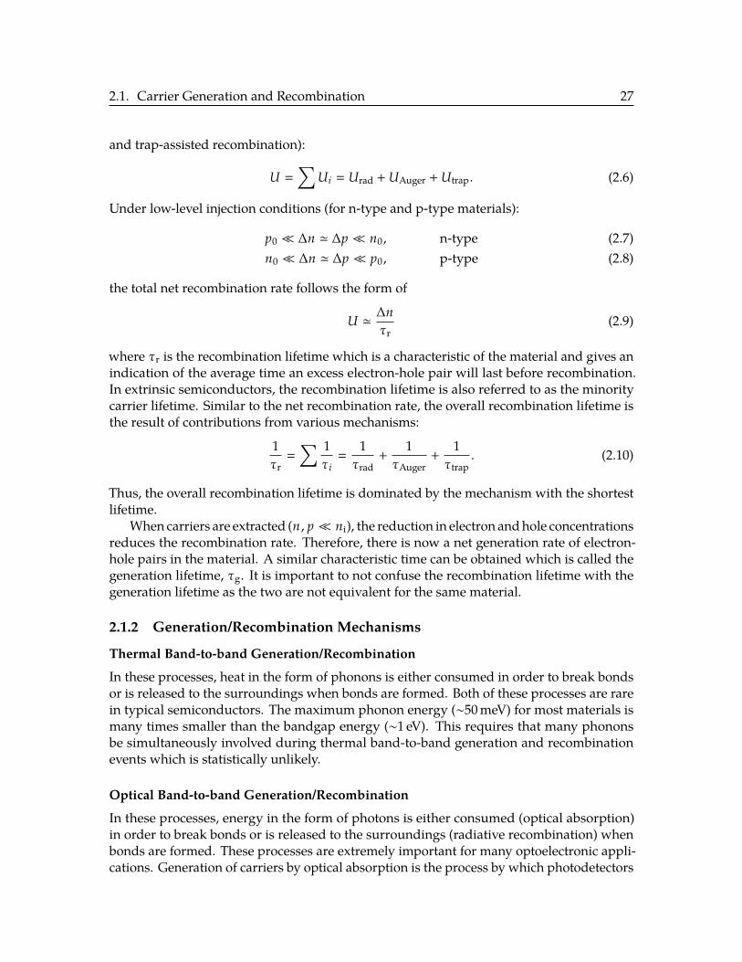
2-1 Generation and recombination mechanisms: (a) Thermal/optical band-to-
band, (b) Auger, and (c) Trap-assisted. . . . . . . . . . . . . . . . . . . . . . . 26
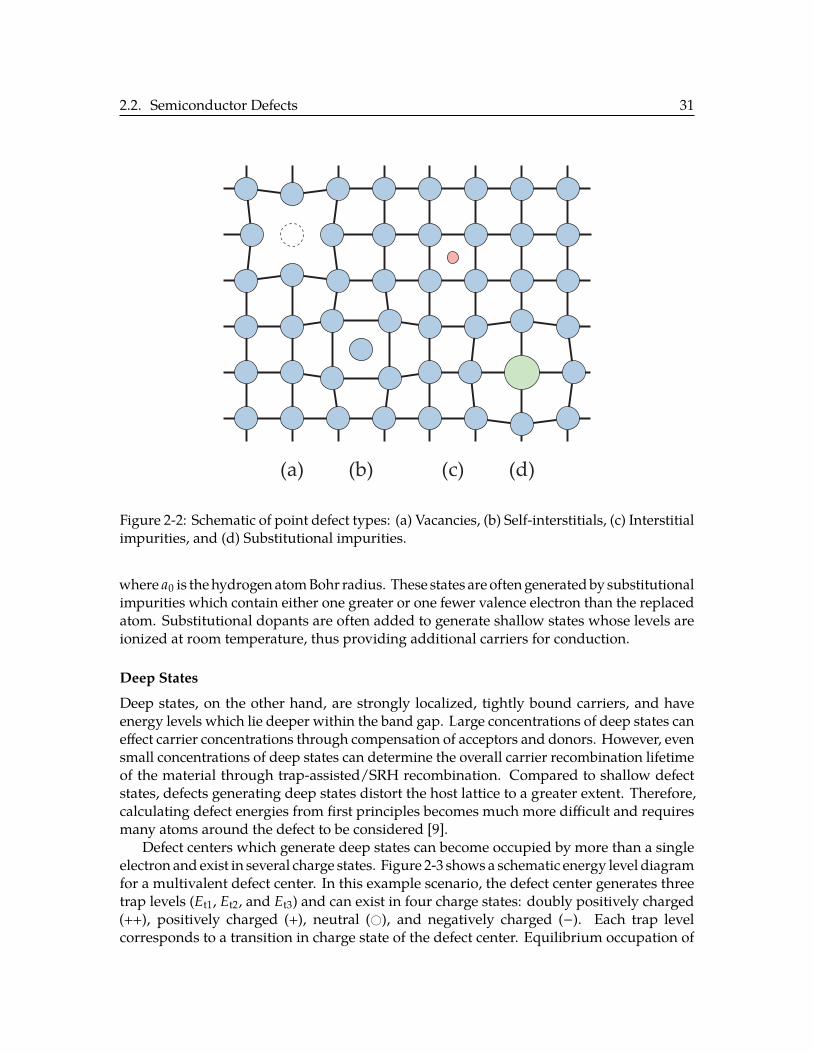
2-2 Schematic of point defect types: (a) Vacancies, (b) Self-interstitials, (c) Inter-
stitial impurities, and (d) Substitutional impurities. . . . . . . . . . . . . . . 31
2-3 Schematic energy level diagram for a multivalent defect center showing
occupation of trap levels for different Fermi level positions. . . . . . . . . . . 32
2-4 Schematic of dislocations formed during heteroepitaxy: (a) Close view of
interface illustrating how misfit dislocations relieve the strain between materi-
als with dissimilar lattice constants; (b) Illustration of threading dislocations
nucleated from misfit segments which extend throughout the film to the
surface. . . . . . . . . . . . . . . . . . . . . . . . . . . . . . . . . . . . . . . . . 33
2-5 Competeing emission (e) and capture (c) process for electrons (n) and holes
(p) at a defect state (Et) within the bandgap. . . . . . . . . . . . . . . . . . . . 35
3-1 Schottky diode bands under neutral and reverse bias conditions . . . . . . . 41
3-2 Schematic representation of the generation of a capacitance transient during
DLTS measurements by emission of majority carriers from defect states in
the depletion region of a diode after voltage pulsing. . . . . . . . . . . . . . 42
3-3 Construction of a DLTS spectrum by implementation of a rate window using
a double boxcar configuration. . . . . . . . . . . . . . . . . . . . . . . . . . . . 44
3-4 Schematic illustrating how a rate window produces a peak in the DLTS
spectrum when the emission rate of the defect state corresponds to the
chosen rate window. . . . . . . . . . . . . . . . . . . . . . . . . . . . . . . . . 45
3-5 Schematic diagram of transition region for a reverse biased Schottky diode
containing deep defect states. . . . . . . . . . . . . . . . . . . . . . . . . . . . 47
3-6 Schematic diagram of our DLTS experimental apparatus showing how a
switch is used to remove the capacitance meter from the circuit during pulsing. 49
3-7 Schematic showing how back contacted samples are mounted within in the
DLTS cryostat to maintain thermal contact while providing electric isolation. 50
3-8 Schematic representation of Frenkel pair production in a crystalline material
after collision of a high energy particle with a lattice atom. . . . . . . . . . . 51
3-9 Scattering probability and kinetic energy transferred as a function of scatter-
ing angle for 1.33 MeV60
Co irradiation. The kinetic energy of the Compton
electron can take any value between 0 and 1.1 MeV. . . . . . . . . . . . . . . 53
14 List of Figures
3-10 Probability density of Compton scattering by 1.33 MeV photons as a function
of the kinetic energy of the scattered electron. . . . . . . . . . . . . . . . . . . 53
3-11 Maximum energy transferred to a lattice atom of silicon or germanium as a
function of the kinetic energy of the scattered electron due to a binary collision.
Previous studies have shown that the energy threshold for one displacement
is approximately 20 eV. For that displacement threshold, Kinchen-Pease
theory predicts that at least 80 eV is required for multiple displacements. If
these thresholds are accurate, then multiple displacements will not occur in
60Co gamma irradiated germanium. . . . . . . . . . . . . . . . . . . . . . . . 54
3-12 DLTS spectrum obtained after60
Co irradiation at 300 K of 1015
cm−3
Sb-
doped germanium showing the generation of four distinct defects. During
measurement, the sample was pulsed for 5 ms from −5 V to 0 V and signal
was collected for a 200 s−1
rate window. . . . . . . . . . . . . . . . . . . . . . 56
3-13 Defect states observed by different groups [30, 31, 33] in studies of Sb-doped
n-type germanium irradiated by varying radiation sources. E37 is observed in
all studies and has previously been assigned to the E-center, a donor-vacancy
pair. Defects with states similar to E30, E22, and E21 have been seen in some
studies but are not consistently detected. . . . . . . . . . . . . . . . . . . . . . 57
3-14 Interstitial containing defect concentrations during room temperature (300 K)
annealing of Ge irradiated at 77 K by60
Co. Annealing duration represents the
time the sample spent above 200 K after irradiation. The concentration of E37,
which accounts for all the vacancies, is constant at 1.7 × 10¹¹
cm−3
Mrad−1
for
the entire annealing duration. Defect concentrations are normalized by the
irradiation dose and are reported in units of cm−3
Mrad−1
. . . . . . . . . . . 60
3-15 Defect concentrations after 15 minute isochronal anneals of60
Co irradiated Sb-
doped germanium. Defect concentrations are normalized by the irradiation
dose and are reported in units of cm−3
Mrad−1
. . . . . . . . . . . . . . . . . . 61
3-16 Defect concentration as a function of annealing duration at 93C. When E22
has annealed out, E21 stops evolving whereas the decay rate of E37 is not
affected. Defect concentrations are normalized by the irradiation dose and
are reported in units of cm−3
Mrad−1
. . . . . . . . . . . . . . . . . . . . . . . . 62
3-17 Annealing rate vs. temperature data extracted from isothermal anneals of
60Co irradiated Sb-doped germanium. Up (↑) and down (↓) arrows next to
defect labels indicate whether the defect concentration increases or decreases
upon annealing. . . . . . . . . . . . . . . . . . . . . . . . . . . . . . . . . . . . 62
3-18 Concentration of interstitials contained in the defects we observe during
room temperature (300 K) annealing of Ge irradiated at 77 K by60
Co. If we
assume that E21 and E30 only contain one interstitial and E22 contains two,
after ∼6 days the number of countable interstitials is constant as the defects
evolve only by changing from one into another. Defect concentrations are
normalized by the irradiation dose and are reported in units of cm−3
Mrad−1
. 67
3-19 Schematic representation of defects in germanium generated by60
Co irra-
diation and their reactions at various temperatures. X, Y, and Z stand for
unknown sinks with which mono-vacancies, V, and self-interstitials, I, react. 70
List of Figures 15
3-20 Schematic of a collision cascade event with differing colors representing
successive generations (primary, secondary, and tertiary) of recoil atoms. . . 71
3-21 SRIM simulation for defect distribution produced by irradiation of Ge with
6 MeV alpha particles. . . . . . . . . . . . . . . . . . . . . . . . . . . . . . . . . 72
3-22 DLTS spectra for neutron irradiated Sb-doped Ge samples. . . . . . . . . . . 74
3-23 Conventional DLTS spectra obtained with varying pulse widths after fast
+ slow neutron irradiation labeled with the names of distinct defect states
identified using Laplace DLTS. . . . . . . . . . . . . . . . . . . . . . . . . . . 74
3-24 Defect states observed after neutron and alpha irradiation of Sb-doped n-type
germanium. . . . . . . . . . . . . . . . . . . . . . . . . . . . . . . . . . . . . . 75
3-25 Linear concentration dependence on dose for defects generated by 6 MeV
alpha irradiation of Ge. . . . . . . . . . . . . . . . . . . . . . . . . . . . . . . . 78
3-26 DLTS spectra from isochronal annealing of 6 MeV alpha irradiated germanium. 78
4-1 The number of transistors per chip has steadily increased demonstrating a
continuation of Moore’s law over time. However, clock speeds saturated in
the early 2000s. Reproduced from [59] . . . . . . . . . . . . . . . . . . . . . . . 80
4-2 Comparison of radiative recombination for (a) direct vs. (b) indirect bandgap
materials. . . . . . . . . . . . . . . . . . . . . . . . . . . . . . . . . . . . . . . . 81
4-3 Schematic band structure of (a) bulk germanium, (b) tensile strained intrinsic
Ge, and (c) tensile strained n+
Ge. . . . . . . . . . . . . . . . . . . . . . . . . . 82
4-4 Schematic of delta doping layers which act as a dopant reservoir for phos-
phorous atoms . . . . . . . . . . . . . . . . . . . . . . . . . . . . . . . . . . . . 85
4-5 Simulation of p+
Si/n+
Ge/n+
Si double heterostructure (a) bands and (b)
carrier concentrations during electrical injection at 1.2 V. . . . . . . . . . . . 86
4-6 Schematic cross-section of the Fabry-Pérot germanium laser structure. . . . 87
4-7 Schematic of the experimental setup used to measure the emission spectra
from Ge laser devices . . . . . . . . . . . . . . . . . . . . . . . . . . . . . . . . 89
4-8 Ge laser emission spectra for varying current densities of a) 90 kA cm−2
and
b) 511 kA cm−2
showing threshold behavior when injected at 800 Hz with
a 4 % duty cycle (50 µs pulse width). Slit width corresponds to a spectral
resolution of∼1.2 nm. Sample had a cavity length of 333 µm and a waveguide
height of ∼100 nm. . . . . . . . . . . . . . . . . . . . . . . . . . . . . . . . . . 90
4-9 L-I curve showing lasing threshold for 270 µm long Ge laser device (λ
1650 nm) injected at 1000 Hz with a 4 % duty cycle (40 µs pulse width). . . . 90
4-10 Emission spectra for various Ge laser devices showing lasing over a wide
wavelength range at (a) 1579 nm, (b) 1622 nm, and (c) 1656 nm. . . . . . . . . 91
4-11 Simulation of gain clamping conditions for Ge Fabry-Pérot lasers showing
how the lasing wavelength changes for varying Ge thicknesses due to different
injection levels being required to overcome modal losses. . . . . . . . . . . . 92
4-12 Plan-view TEM of the Ge material in laser devices after dopant drive-in ther-
mal treatment of 750C for 1 min showing an average threading dislocation
density of ∼1.9 × 10⁹
cm−2
. . . . . . . . . . . . . . . . . . . . . . . . . . . . . . 94
16 List of Figures
4-13 Estimation of non-radiative lifetimes and threshold current increases due to
varying threading dislocation densities. Non-radiative lifetime is approxi-
mately equal to the radiative lifetime for a TDD of ∼4 × 10⁷
cm−2
. . . . . . . 96
5-1 Schematic illustrating the two methods of resonant optical sensing based on
observing changes in the complex refractive index. . . . . . . . . . . . . . . . 100
5-2 Schematic representation of a QD-doped ChG light source integrated with
an optical sensor system built on a ChG platform. . . . . . . . . . . . . . . . 100
5-3 Schematic of PbS colloidal quantum dot synthesis through hot injection.
Bis(trimethylsilyl)sulfide intrioctylphosphine is quickly injected into a care-
fully temperature controlled precursor solution containing PbO and oleic
acid. The PbO reduces and reacts to nucleate PbS QDs whose growth quickly
self terminates through passivation of the QDs by oleic acid ligands. Fur-
ther materials can be added to the solution after QD nucleation to grow
semiconductor shells to tailor electronic properties and provide extra surface
passivation. . . . . . . . . . . . . . . . . . . . . . . . . . . . . . . . . . . . . . 102
5-4 Optical micrographs of thin films fabricated from solutions of As2S3 in PA
(a) without and (b) with PbS QDs . . . . . . . . . . . . . . . . . . . . . . . . . 106
5-5 Photoluminescence spectra comparing PbS QDs (λc ≈ 1300 nm) embedded
in PMMA and ChG (Ge23Sb7S70) matrices. Samples were excited by a CW
633 nm laser. . . . . . . . . . . . . . . . . . . . . . . . . . . . . . . . . . . . . . 107
5-6 Micro-PL spectra comparing emission from areas containing QD aggregates
to areas without QD aggregates in films of PbS QDs (λc ≈ 1650 nm) embed-
ded in As2S3. . . . . . . . . . . . . . . . . . . . . . . . . . . . . . . . . . . . . . 108
5-7 Optical micrograph of a thin film fabricated from AsS3
3–
capped QDs em-
bedded in As2S3. . . . . . . . . . . . . . . . . . . . . . . . . . . . . . . . . . . 109
5-8 Micro PL spectra comparing emission from QDs with AsS3
3–
ligands embed-
ded in As2S3 vs drop casted solutions of QDs with oleic acid ligands. . . . . 109
6-1 Theoretical solar spectrum losses for a single junction Si solar cell. . . . . . . 112
6-2 Schematic of singlet exciton fission process where (a) initial excitation of a
chromophore generates S1 which (b) subsequently shares its energy with a
nearby chromophore in S0 state to generate T1 triplet states on both. . . . . . 114
6-3 Schematic illustrating the potential benefit of adding a singlet exciton fission
layer (e.g., Tetracene) to a Si solar cell. . . . . . . . . . . . . . . . . . . . . . . 115
6-4 Sample representation of internal quantum efficiency (IQE) vs. wavelength
for a typical Si solar cell with varying front surface recombination velocities
(102
cm s−1
to 106
cm s−1
). Corresponding absorption depths for light in Si
are plotted on the top x-axis. The red region represents the wavelength range
that is absorbed by tetracene. . . . . . . . . . . . . . . . . . . . . . . . . . . . 117
6-5 IQE for (a) surface carriers and (b) λ 530 nm for varying emitter thicknesses
and front surface SRV for a conventional Si solar cell design. . . . . . . . . . 119
6-6 Changes in IQE resulting from addition of tetracene for varying emitter
thickness and SRV for a conventional Si solar cell design. . . . . . . . . . . . 120
List of Figures 17
6-7 Changes in IQE for (a) 100 nm and (b) 1 µm emitter thickness for varying
triplet transfer efficiencies and SRV for a conventional Si solar cell design. . 121
6-8 IQE for (a) surface carriers and (b) λ 530 nm for varying bulk lifetimes and
SRV for a backside illuminated Si solar cell design . . . . . . . . . . . . . . . 123
6-9 Changes in IQE resulting from addition of tetracene for varying bulk lifetimes
and SRV for a backside illuminated Si solar cell design. . . . . . . . . . . . . 124
6-10 Changes in IQE for varying triplet transfer efficiencies and SRV for a backside
illuminated Si solar cell design (assuming 1000 µs lifetimes). . . . . . . . . . 124
6-11 Schematic of RFPCD experimental apparatus. . . . . . . . . . . . . . . . . . . 125
6-12 Schematic of RFPCD signal output during measurement illustrating how the
signal depends on carrier lifetimes and generation rates. . . . . . . . . . . . 126
6-13 Schematic of RFPCD transfer yield measurements by comparison of genera-
tion rates for samples with and without tetracene. . . . . . . . . . . . . . . . 128
6-14 Example of using magnetic field effect measurements to identify triplet con-
tributions to signal as seen for fluorescence and photocurrent from tetracene
based organic solar cells. . . . . . . . . . . . . . . . . . . . . . . . . . . . . . . 129
6-15 Comparison of lifetimes (850 nm excitation) from 1" x 1" Si wafer pieces
(5 × 10¹⁴
cm−3
n-type) when (a) immersed in HF to form a well passivated
surface and (b) left bare and with a 20 nm tetracene film. . . . . . . . . . . . 130
6-16 Schematic of the various reactions involved in the transfer of triplet exciton
energy into silicon: (a) Singlet exciton fission, (b) triplet diffusion to the
interface, (c) transfer of triplet state energy into acceptor state in silicon
forming electron-hole pair, (d) dissociation of electron-hole pair into free
carriers, (e) singlet diffusion to the interface, and (f) transfer of singlet state
energy into acceptor state in silicon forming electron-hole pair. The described
reactions are reversible and have corresponding backward reactions. . . . . 131
6-17 Estimation of triplet transfer rate dependence on barrier width by approxi-
mating transfer as tunneling through a finite potential barrier. . . . . . . . . 133
6-18 Estimation of triplet transfer efficiency on barrier width. . . . . . . . . . . . 133
6-19 Effective carrier lifetimes measured via RFPCD for films deposited by ALD
for varying film thicknesses. . . . . . . . . . . . . . . . . . . . . . . . . . . . . 136
6-20 Magnetic Field Effect (MFE) PL from ALD passivated samples showing
transfer of triplet energy into Si. . . . . . . . . . . . . . . . . . . . . . . . . . . 137
6-21 Photoluminescence spectra comparison show that emission from tetracene
coated Si matches that of bare Si. . . . . . . . . . . . . . . . . . . . . . . . . . 138
6-22 Generation rate ratios measured by RFPCD for thick dry oxides. . . . . . . . 139

18 List of Figures

List of Tables
3.1 Summary of defect states in60
Co irradiated Sb-doped germanium . . . . . . 58
3.2 Summary of reaction parameters extracted from isothermal anneals . . . . . 63
3.3 Conversion ratio of E22 to E21 . . . . . . . . . . . . . . . . . . . . . . . . . . . 67
3.4 Summary of defect states observed after neutron and alpha irradiation of
Sb-doped germanium . . . . . . . . . . . . . . . . . . . . . . . . . . . . . . . . 76
4.1 Summary of Electrically Pumped Ge-on-Si Laser Specifications . . . . . . . 92
5.1 Comparison of solvents for ChG solution processing . . . . . . . . . . . . . . 104
5.2 Comparison of ChG and QD solubility in amines . . . . . . . . . . . . . . . . 105
6.1 Summary of results from fabrication of thin oxide films via dry oxidation . 135

20 List of Tables
Chapter 1
Introduction
Optoelectronic components perform conversions between optical and electrical energy and
are used to generate (e.g., lasers and LEDs), control (e.g., optical modulators), and detect (e.g.,
photodiodes and CCDs) light. In recent years, optoelectronics have had a surge in interest
due to the increasing importance of optoelectronics for computing applications. Advances
in computing have largely been a result of reductions in component sizes within integrated
circuits over time. As this process moves components to even smaller dimensions, electrical
interconnects become a bottleneck to increased performance [1]. Optical communications
via optoelectronic devices and fiber optics have allowed for the transmission of data
over long distances with high bandwidth. As bottlenecks in electronic circuit scaling
become more problematic, using optical communications on shorter length scales becomes
necessary for increased performance scaling. Integration of electronics with microphotonic
optoelectronic interconnect systems can provide higher bandwidth density, lower energy
costs, and increased resistance to electromagnetic interference [2]. For use in practical
applications, the fabrication of microphotonic components must be compatible with CMOS
process flows. The obvious materials choice for building a microphotonic platform is silicon
due to its ubiquity in the microelectronics industry. High volume fabrication processes
methods developed by the semiconductor industry can be leveraged for high volume
integration of silicon photonics with silicon microelectronics at low cost [3]. In addition to
improved computing scaling, integrated optoelectronics also have applications in a variety
of other fields such as imaging [4] and chemical/biological species sensing [5].
Optoelectronic devices are minority carrier devices and whose operation is strongly
influenced by recombination and generation processes which are dominated in germa-
nium (Ge) and silicon (Si) by defects. Chapter 2 briefly introduces semiconductor concepts
relevant to understanding the impact of defects on optoelectronic applications. Of par-
ticular importance is understanding the influence of defect related trap states on carrier
recombination-generation processes. In this thesis, we look at a few systems where under-
standing various material defects are beneficial for improving optoelectronic performance.
Chapter 3 focuses on the characterization of point defects in germanium. Germanium
forms the basis for mature modulator and photodetector technologies and shows poten-
tial for development of a Si photonics monolithically integrated light source. Many of
the photodetectors used in long-range telecom systems and mid-range data centers are
22 Chapter 1. Introduction
germanium-based. Even though germanium was used for many of the first semiconductor
studies and devices, it has largely been supplanted by silicon for microelectronics applica-
tions. However, germanium has recently seen renewed interest partially due to the surge in
Si photonics for which germanium provides a CMOS-compatible active material which can
be integrated with passive Si photonic components. In addition, the high hole mobilities of
germanium have renewed interest in developing Ge computing circuits as silicon devices
start to approach theoretical limits. Compared to silicon, relatively little is understood
about point defect states in germanium which act as generation-recombination centers and
limit the performance of devices. We use a variety of radiation sources to generate vacancies
and interstitials in germanium. The generated vacancies and interstitials diffuse and react
with each other or impurities resulting in the formation of stable defect associates which
we characterize by deep-level transient spectroscopy (DLTS). Annealing studies were also
performed to determine the kinetics of various defect reactions. Electronic characterization
(from DLTS) together with the reaction kinetics are analyzed in order to make tentative
assignments for the identity of some defect states.
Out of all the components in a microphotonic circuit, fabrication of an integrated light
source currently poses the largest challenge. Chapter 4 shows successfully demonstration
of electrically pumped lasing from germanium. This system provides a monolithically
integrable solution for a Si photonics compatible light source for optical interconnect
applications. Germanium is epitaxially grown on silicon with tensile strain and is highly
n-type doped in order to engineering the bandgap to be pseudo-direct. Heteroepitaxy of
Ge-on-Si requires relaxation of strain through nucleation of dislocations which become
the dominant defect in this system. Threshold current densities for our Ge lasers are
approximately two orders of magnitude greater than for traditional III-V laser diodes. In
order to understand the observed behavior, we develop a model to determine the impact of
recombination at dislocations on laser performance.
Chapter 5 investigates a potential materials system for fabrication of substrate-independent
integrated light sources. We develop the processes needed to solution process colloidal
quantum dot (QD) chalcogenide glass (ChG) composite thin films by investigating the in-
terface between QD surfaces and the ChG matrix. This system provides a wide bandwidth,
substrate independent platform for developing light sources that can be integrated easily
with ChG-based optical sensor microphotonic systems.
Chapter 6 focuses on investigating the transfer of triplet exciton energy from tetracene to
silicon. Due to increasing worry about the impact of CO2 emissions from burning fossil fuels,
photovoltaics are another optoelectronic application that have seen a recent surge in interest.
Even though silicon has a bandgap close to ideal for a single junction cell, due to theoretical
limitations, the overall efficiency for a silicon solar cell is limited to ∼32 %. A significant
portion of the incident solar energy is lost by thermalization of carriers generated by photons
with energies greater than the bandgap. Tetracene is an organic semiconductor material
which can absorb high energy photons to generate singlet excitons. These singlet excitons
can undergo singlet exciton fission to generated two triplet excitons with approximately half
the energy. If that energy from the two triplet excitons can be efficiently transfered to a silicon
solar cell to generate two electron-hole pairs, this would effectively double the photocurrent
from high energy photons. An important factor in determining whether a practical increase
in efficiency can be gained is the interface between silicon and tetracene. We model what
23
surface recombination velocities are required for transfer to be useful assuming that transfer
of energy from tetracene to silicon places carriers closer to the surface than they would be
in a traditional cell design. We also experimentally investigate and demonstrate transfer
of triplet exciton energy to silicon which has not previously been conclusively shown to
occur. Experimental characterization of recombination at the interface between silicon and
tetracene is crucial to understanding and improving energy transfer. We use contactless
radio frequency photoconductivity decay (RFPCD) measurements to quickly characterize
the quality of interfaces and also develop a methodology for observing transfer of energy
from tetracene to silicon (via RFPCD).
Chapter 7 summarizes the key accomplishments of the work presented in this thesis.

24 Chapter 1. Introduction
Chapter 2
Semiconductor Concepts
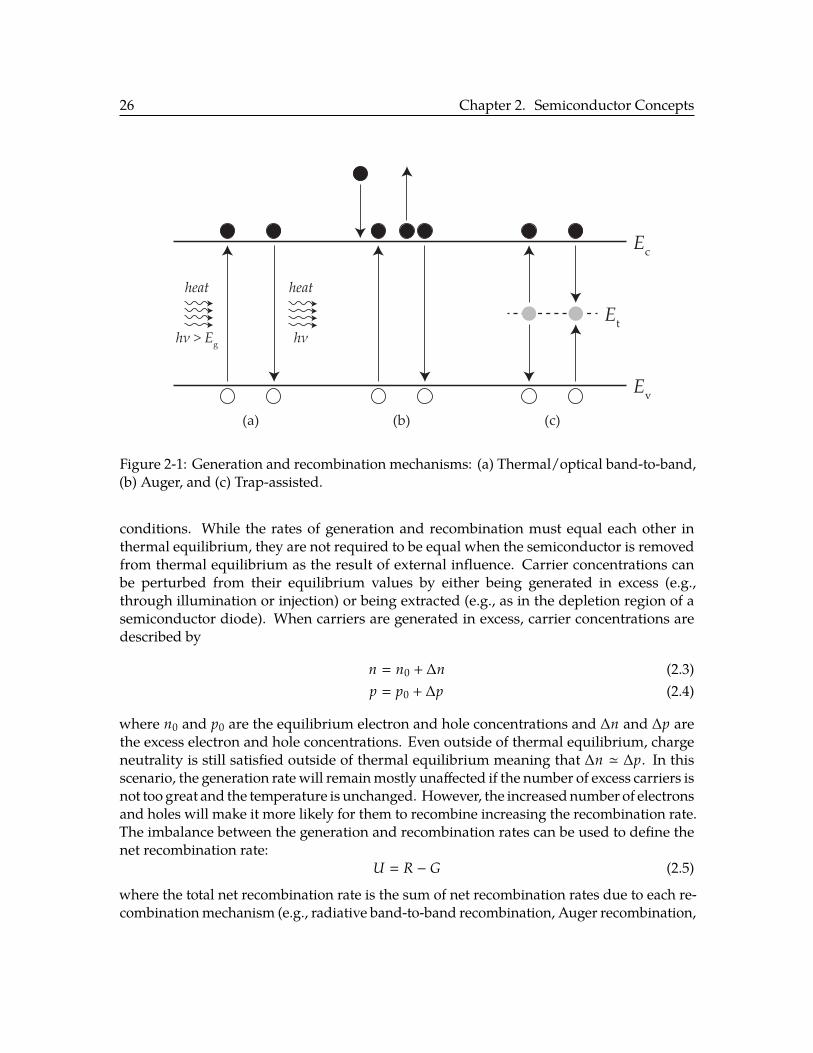
2.1 Carrier Generation and RecombinationWhen a semiconductor is in thermal equilibrium, a dynamic balance between generation and
recombination of carriers is present. Electrons and holes are continuously being generated
and are also recombining to annihilate each other. Generation and recombination occurs
through the following mechanisms (Figure 2-1):
1. Thermal band-to-band generation/recombination
2. Optical band-to-band generation/recombination
3. Auger generation/recombination
4. Trap-assisted generation/recombination
A semiconductor is in thermal equilibrium when there is no exchange of energy outside
the system and the system is in steady state. Under these conditions, the following balance
is established:
G R (2.1)
where G is the generation rate (number of electron-hole pairs created per unit volume per
time, cm−3
s−1
) and R is the recombination rate (number of electron-hole recombination
events per unit volume per time, cm−3
s−1
). Because multiple pathways are present for
generation and recombination, the overall generation and recombination rates are the sum
of the individual rates. Moreover, the existence of multiple pathways requires that the
system satisfy the principle of detailed balance in thermal equilibrium which states that
the rates of a process and its inverse must equal and balance in detail:
Gi Ri for all i (2.2)
where the subscript i indicates a specific generation/recombination mechanism.
2.1.1 Carrier Lifetimes
For semiconductors, the carrier lifetime can refer to both the generation lifetime and
the recombination lifetime. These parameters are most relevant outside of equilibrium
26 Chapter 2. Semiconductor Concepts
Ec
Ev
Et
heat heat
hν > Eg hν
(a) (b) (c)
Figure 2-1: Generation and recombination mechanisms: (a) Thermal/optical band-to-band,
(b) Auger, and (c) Trap-assisted.
conditions. While the rates of generation and recombination must equal each other in
thermal equilibrium, they are not required to be equal when the semiconductor is removed
from thermal equilibrium as the result of external influence. Carrier concentrations can
be perturbed from their equilibrium values by either being generated in excess (e.g.,
through illumination or injection) or being extracted (e.g., as in the depletion region of a
semiconductor diode). When carriers are generated in excess, carrier concentrations are
described by
n n0 + ∆n (2.3)
p p0 + ∆p (2.4)
where n0 and p0 are the equilibrium electron and hole concentrations and ∆n and ∆p are
the excess electron and hole concentrations. Even outside of thermal equilibrium, charge
neutrality is still satisfied outside of thermal equilibrium meaning that ∆n ' ∆p. In this
scenario, the generation rate will remain mostly unaffected if the number of excess carriers is
not too great and the temperature is unchanged. However, the increased number of electrons
and holes will make it more likely for them to recombine increasing the recombination rate.
The imbalance between the generation and recombination rates can be used to define the
net recombination rate:
U R − G (2.5)
where the total net recombination rate is the sum of net recombination rates due to each re-
combination mechanism (e.g., radiative band-to-band recombination, Auger recombination,
2.1. Carrier Generation and Recombination 27
and trap-assisted recombination):
U
∑Ui Urad + UAuger + Utrap. (2.6)
Under low-level injection conditions (for n-type and p-type materials):
p0 ∆n ' ∆p n0 , n-type (2.7)
n0 ∆n ' ∆p p0 , p-type (2.8)
the total net recombination rate follows the form of
U '∆nτr
(2.9)
where τr is the recombination lifetime which is a characteristic of the material and gives an
indication of the average time an excess electron-hole pair will last before recombination.
In extrinsic semiconductors, the recombination lifetime is also referred to as the minority
carrier lifetime. Similar to the net recombination rate, the overall recombination lifetime is
the result of contributions from various mechanisms:
1
τr
∑1
τi
1
τrad
+1
τAuger
+1
τtrap
. (2.10)
Thus, the overall recombination lifetime is dominated by the mechanism with the shortest
lifetime.
When carriers are extracted (n , p ni), the reduction in electron and hole concentrations
reduces the recombination rate. Therefore, there is now a net generation rate of electron-
hole pairs in the material. A similar characteristic time can be obtained which is called the
generation lifetime, τg. It is important to not confuse the recombination lifetime with the
generation lifetime as the two are not equivalent for the same material.
2.1.2 Generation/Recombination Mechanisms
Thermal Band-to-band Generation/Recombination
In these processes, heat in the form of phonons is either consumed in order to break bonds
or is released to the surroundings when bonds are formed. Both of these processes are rare
in typical semiconductors. The maximum phonon energy (∼50 meV) for most materials is
many times smaller than the bandgap energy (∼1 eV). This requires that many phonons
be simultaneously involved during thermal band-to-band generation and recombination
events which is statistically unlikely.
Optical Band-to-band Generation/Recombination
In these processes, energy in the form of photons is either consumed (optical absorption)
in order to break bonds or is released to the surroundings (radiative recombination) when
bonds are formed. These processes are extremely important for many optoelectronic appli-
cations. Generation of carriers by optical absorption is the process by which photodetectors
28 Chapter 2. Semiconductor Concepts
and photovoltaic cells operate. Light emission by radiative recombination is the process by
which light emitting diodes (LEDs) and semiconductor diode lasers operate.
Because band-to-band processes require both conservation of energy and momentum,
the rate of optical band-to-band processes can vary greatly depending on whether the
material has a direct or indirect bandgap. In direct bandgap materials, conservation
of momentum is easily satisfied for band-to-band transisitions. Therefore, the rates of
these processes can be quite large in direct bandgap materials. However, in indirect
bandgap materials (such as Si and Ge), a phonon is required in order to satisfy momentum
conservation during band-to-band transitions. Therefore, the rates of optical generation
and recombination processes are much smaller in indirect bandgap materials than in direct
bandgap materials.
Generation produces carriers by the breaking of bonds and is therefore dependent on
the number of available bonds in the material. Practically speaking, this supply can be
considered to be unlimited. Recombination on the other hand requires the presence of
free electrons and holes and thus depends on the carrier concentrations. Outside of the
equilibrium conditions, the net reaction rates are described by
−Urad Grad − Rrad ' kradn2
iextracted carriers (2.11)
Urad Rrad − Grad krad
(np − n0p0
)excess carriers (2.12)
where krad is a temperature dependent reaction rate constant characteristic of the material.
This relationship shows that the net recombination rate is proportional to the excess npproduct.
Auger Generation/Recombination
Auger processes involve “hot” carriers which have large kinetic energy. Auger generation
occurs when carriers transfer some of their excess kinetic energy to a bond, thereby breaking
it and generating an electron-hole pair. Auger recombination occurs when a recombination
event transfers the energy released from electron-hole recombination to a third carrier
(which now has excess kinetic energy). Because Auger recombination requires a third carrier,
it is typically an unlikely recombination mechanism. However, when the concentration of
carriers is large (for heavily-doped semiconductors or under carrier injection conditions),
the probability of Auger recombination occurring increases potentially making this an
important recombination pathway.
Unlike band-to-band generation, the supply of reactants cannot be considered unlimited.
Because the probability of a carrier containing sufficient energy for Auger processes in-
creases with carrier concentration, the Auger generation rate is proportional to the relevant
carrier concentration. The Auger recombination rate requires three carriers and is thus
proportional to the square of the relevant carrier concentration times the concentration of
the complementary carrier. For a Auger processes, the net reaction rates are described by
−UAuger
(khen + khhp
)n2
iextracted carriers (2.13)
UAuger
(khen + khhp
) (np − n0p0
)excess carriers (2.14)

2.2. Semiconductor Defects 29
where khe and khh are temperature dependent reaction rate constants characteristic of the
material for hot-electron and hot-hole processes, respectively. Similar to band-to-band
processes, the net recombination rate is proportional to the excess np product. Auger
generation under extracted carrier conditions is extremely unlikely due to the lack of
carriers.
Trap-assisted (SRH) Generation/Recombination
Defects within the semiconductor material can produce trap states (Section 2.2) which can
greatly enhance thermal generation and recombination of carriers. These processes are
also referred to as Shockley-Read-Hall (SRH) processes based on the models developed by
Shockley and Read [6] and Hall [7, 8]. During trap-assisted recombination, one carrier type
can become “trapped” at a localized site until the complementary carrier is present making
it much more likely that recombination will occur. This is particularly important in indirect
bandgap materials because while the trap site is localized in the lattice, it is delocalized
in k-space making it easier to satisfy momentum conservation. In addition, compared
to band-to-band processes, trap-assisted processes require substantially less energy. In
fact, this is typically the most dominant mechanism for generation and recombination in
microelectronic devices. For trap-assisted processes, the net recombination reaction rate is
described by
Utrap np − n2
i
1
σp〈vp〉Nt
(n + ni exp
Et−Ei
kT
)+
1
σn〈vn〉Nt
(p + ni exp
Ei−Et
kT
) (2.15)
where σn and σp are the capture cross sections for electrons and holes, ni is the intrinsic
carrier concentration, Nt is the number of trap states, Et is the energy of the trap level, Ei is
the intrinsic Fermi level and 〈vn,p〉 is the mean thermal velocity of carriers given by
〈vn,p〉
√3kTm∗
n,p(2.16)
where m∗n,p is the effective mass of conductivity for the relevant carrier.
2.2 Semiconductor DefectsSemiconductor electronic properties are determined by the band structure which is related
to the crystal structure. Crystallographic lattice defects are perturbations to the structure
which in turn modify in the band structure altering the properties of the material. Because
defects have a large impact on the properties of the material, understanding their behavior
is crucial. The inclusion of a small number of defects is thermodynamically favorable and
unavoidable. For almost all semiconductor applications, defects are intentionally introduced
in the form of dopants. In addition, deleterious defects are often inadvertently introduced
during fabrication and processing limiting device performance. Therefore, knowledge of
defects and how they impact properties can be used to both reduce device degradation and
30 Chapter 2. Semiconductor Concepts
engineer the properties of a material and open up uses for new applications. Lattice defects
can be classified based on their dimensionality into the following groups:
1. Zero-Dimensional Defects (Point Defects)
2. One-Dimensional Defects (Dislocations)
3. Two-Dimensional Defects (Surfaces, Grain Boundaries, Stacking Faults, etc.)
4. Three-Dimensional Defects (Clusters, Precipitates, Voids, etc.)
A few of the defect types most relevant to this thesis will be described in the following
sections:
2.2.1 Point Defects
Zero-dimensional defects involve atomic-sized perturbations from the ideal lattice and are
often referred to as point defects. Within this classification there are a variety of defect
types (Figure 2-2). A vacancy is the absence of an atom from a lattice site. An interstitial
is an atom which is located at a site which is not part of the host lattice. Interstitials
can either be composed from an atom of the host material (self-interstitial) or from an
impurity atom. Impurity atoms can also be located at lattice sites forming substitutional
defects. Semiconductor carrier concentrations are often precisely controlled by introduction
of substitutional impurities with one greater or one fewer valence electron (acceptors and
donors). These defects can also react with each other to form defect associates (also referred
to as defect complexes) such as di-interstitials or vacancy-donor associates.
Point defects are a large focus of this thesis due to the impact (Section 2.3.1) of the
bandgap states they generate. These states can be further classified as either shallow states
or deep states:
Shallow States
Point defect states are often divided into two categories: shallow states (ionization energies
/ 50 meV) and deep states (ionization energies ' 50 meV). Shallow states form levels close
to the relevant band edges (valence band for acceptors and conduction band for donors) and
are sometimes referred to as hydrogenic defect states because they form levels similar to
that of a hydrogen atom. However, the energy levels are modified since the hydrogen-like
impurities are contained in a crystalline material . A modified Rydberg binding energy can
be calculated by accounting for dielectric screening by the host and using the effective mass
of the relevant band edge:
E m∗
meε2
r
·13.6
n2
eV (2.17)
where m∗ is the effective mass of the carrier, me is the electron rest mass, εr is the relative
permittivity (dielectric constant), and n is the principle quantum number. Similar to a
hydrogen atom, carriers are weakly bound by a Coulombic potential. An analogous Bohr
radius can be calculated and is typically equal to several lattice spacings:
aB εr
me
m∗a0 (2.18)
2.2. Semiconductor Defects 31
(a) (b) (c) (d)
Figure 2-2: Schematic of point defect types: (a) Vacancies, (b) Self-interstitials, (c) Interstitial
impurities, and (d) Substitutional impurities.
where a0 is the hydrogen atom Bohr radius. These states are often generated by substitutional
impurities which contain either one greater or one fewer valence electron than the replaced
atom. Substitutional dopants are often added to generate shallow states whose levels are
ionized at room temperature, thus providing additional carriers for conduction.
Deep States
Deep states, on the other hand, are strongly localized, tightly bound carriers, and have
energy levels which lie deeper within the band gap. Large concentrations of deep states can
effect carrier concentrations through compensation of acceptors and donors. However, even
small concentrations of deep states can determine the overall carrier recombination lifetime
of the material through trap-assisted/SRH recombination. Compared to shallow defect
states, defects generating deep states distort the host lattice to a greater extent. Therefore,
calculating defect energies from first principles becomes much more difficult and requires
many atoms around the defect to be considered [9].
Defect centers which generate deep states can become occupied by more than a single
electron and exist in several charge states. Figure 2-3 shows a schematic energy level diagram
for a multivalent defect center. In this example scenario, the defect center generates three
trap levels (Et1, Et2, and Et3) and can exist in four charge states: doubly positively charged
(++), positively charged (+), neutral (#), and negatively charged (−). Each trap level
corresponds to a transition in charge state of the defect center. Equilibrium occupation of
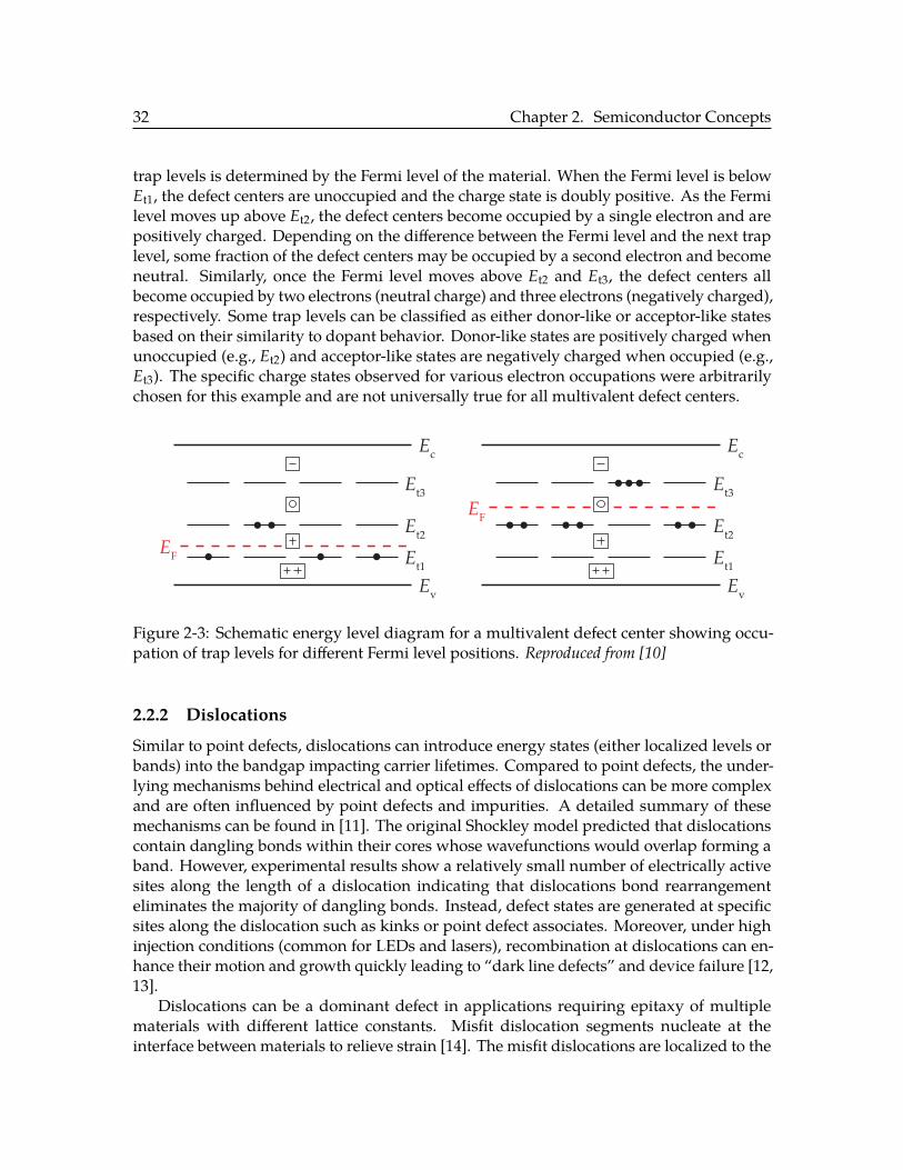
32 Chapter 2. Semiconductor Concepts
trap levels is determined by the Fermi level of the material. When the Fermi level is below
Et1, the defect centers are unoccupied and the charge state is doubly positive. As the Fermi
level moves up above Et2, the defect centers become occupied by a single electron and are
positively charged. Depending on the difference between the Fermi level and the next trap
level, some fraction of the defect centers may be occupied by a second electron and become
neutral. Similarly, once the Fermi level moves above Et2 and Et3, the defect centers all
become occupied by two electrons (neutral charge) and three electrons (negatively charged),
respectively. Some trap levels can be classified as either donor-like or acceptor-like states
based on their similarity to dopant behavior. Donor-like states are positively charged when
unoccupied (e.g., Et2) and acceptor-like states are negatively charged when occupied (e.g.,
Et3). The specific charge states observed for various electron occupations were arbitrarily
chosen for this example and are not universally true for all multivalent defect centers.
Ec
Ev
Et1
Et2
Et3
Ec
Ev
Et1
Et2
Et3
EF
EF
Figure 2-3: Schematic energy level diagram for a multivalent defect center showing occu-
pation of trap levels for different Fermi level positions. Reproduced from [10]
2.2.2 Dislocations
Similar to point defects, dislocations can introduce energy states (either localized levels or
bands) into the bandgap impacting carrier lifetimes. Compared to point defects, the under-
lying mechanisms behind electrical and optical effects of dislocations can be more complex
and are often influenced by point defects and impurities. A detailed summary of these
mechanisms can be found in [11]. The original Shockley model predicted that dislocations
contain dangling bonds within their cores whose wavefunctions would overlap forming a
band. However, experimental results show a relatively small number of electrically active
sites along the length of a dislocation indicating that dislocations bond rearrangement
eliminates the majority of dangling bonds. Instead, defect states are generated at specific
sites along the dislocation such as kinks or point defect associates. Moreover, under high
injection conditions (common for LEDs and lasers), recombination at dislocations can en-
hance their motion and growth quickly leading to “dark line defects” and device failure [12,
13].
Dislocations can be a dominant defect in applications requiring epitaxy of multiple
materials with different lattice constants. Misfit dislocation segments nucleate at the
interface between materials to relieve strain [14]. The misfit dislocations are localized to the
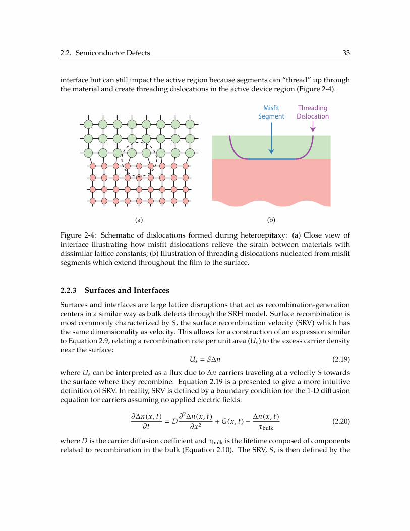
2.2. Semiconductor Defects 33
interface but can still impact the active region because segments can “thread” up through
the material and create threading dislocations in the active device region (Figure 2-4).
(a)
MisfitSegment
ThreadingDislocation
(b)
Figure 2-4: Schematic of dislocations formed during heteroepitaxy: (a) Close view of
interface illustrating how misfit dislocations relieve the strain between materials with
dissimilar lattice constants; (b) Illustration of threading dislocations nucleated from misfit
segments which extend throughout the film to the surface.
2.2.3 Surfaces and Interfaces
Surfaces and interfaces are large lattice disruptions that act as recombination-generation
centers in a similar way as bulk defects through the SRH model. Surface recombination is
most commonly characterized by S, the surface recombination velocity (SRV) which has
the same dimensionality as velocity. This allows for a construction of an expression similar
to Equation 2.9, relating a recombination rate per unit area (Us) to the excess carrier density
near the surface:
Us S∆n (2.19)
where Us can be interpreted as a flux due to ∆n carriers traveling at a velocity S towards
the surface where they recombine. Equation 2.19 is a presented to give a more intuitive
definition of SRV. In reality, SRV is defined by a boundary condition for the 1-D diffusion
equation for carriers assuming no applied electric fields:
∂∆n(x , t)∂t
D∂2∆n(x , t)
∂x2
+ G(x , t) −∆n(x , t)τbulk
(2.20)
where D is the carrier diffusion coefficient and τbulk is the lifetime composed of components
related to recombination in the bulk (Equation 2.10). The SRV, S, is then defined by the
34 Chapter 2. Semiconductor Concepts
following boundary condition (in steady-state,∂n∂t 0)
Dd∆n(x)
dx
x0
S∆n(x 0). (2.21)
When surfaces contribute to recombination, is it useful to describe an effective recombi-
nation lifetime which includes bulk and surface lifetime, τsurf, components:
1
τeff
1
τbulk
+1
τsurf
(2.22)
where τsurf is related to S by
1
τsurf
β2D (2.23)
where β can be obtained from a solution of
β tan
(βd2
)
SD
(2.24)
where d is the sample thickness [15]. It should be noted that this equation is derived for the
condition that S for both front and back surfaces are equal. In the limits of low and high
surface recombination velocity
τsurf(S → 0) d
2S(2.25)
τsurf(S →∞) d2
π2D. (2.26)
If τbulk and S are both large, then the effective carrier lifetime reduces to Equation 2.26
meaning that the observed lifetime is simply the average time it takes for carriers to diffuse
to the surface.
2.3 Dynamic Behavior of Deep Defect StatesThe dynamic electronic behavior of deep states are controlled by four competing processes
(Figure 2-5):
1. Electron emission into the conduction band (en)
2. Electron capture into non-occupied deep states (cn)
3. Hole capture into electron occupied deep states (cp)
4. Hole emission into the valence band (ep)
Electrons are emitted from and holes are captured at nt sites occupied by electrons while
holes are emitted from and electrons are captured at (Nt − nt) unoccupied sites. Thus, the
rate of change of electron occupancy at a defect state is
dnt
dt (ep + cn)(Nt − nt) − (en + cp)nt (2.27)
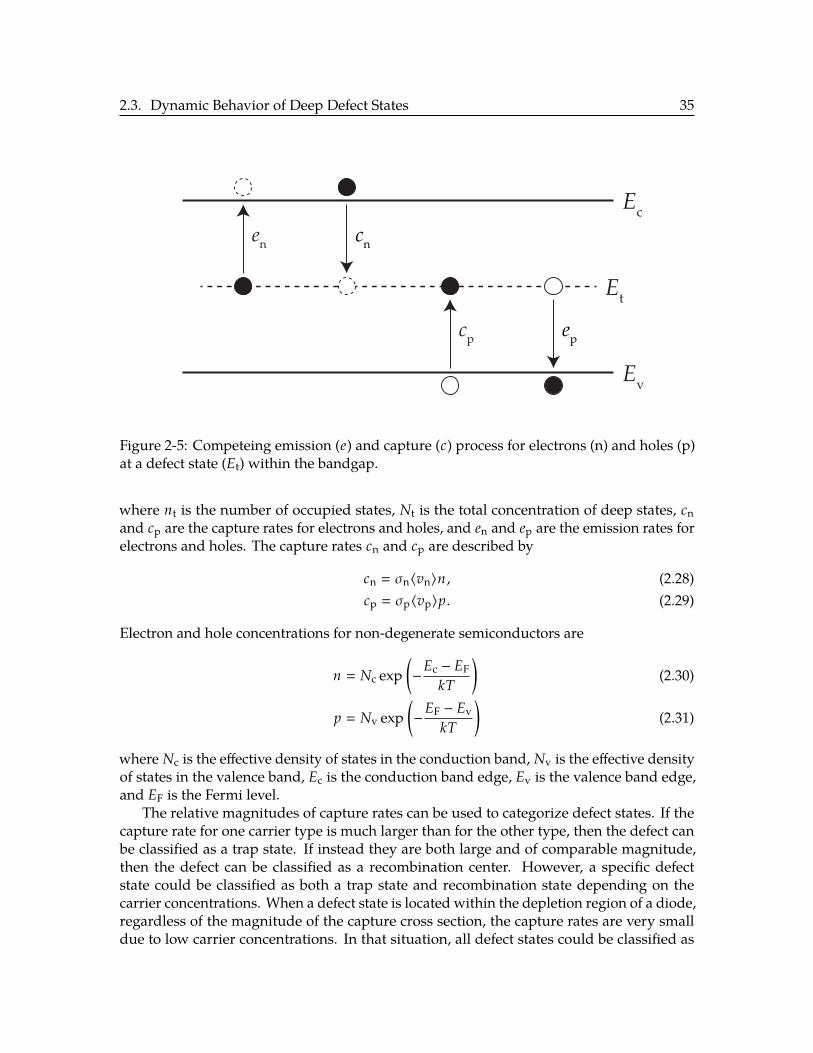
2.3. Dynamic Behavior of Deep Defect States 35
Ec
Ev
Et
en cn
cp ep
Figure 2-5: Competeing emission (e) and capture (c) process for electrons (n) and holes (p)
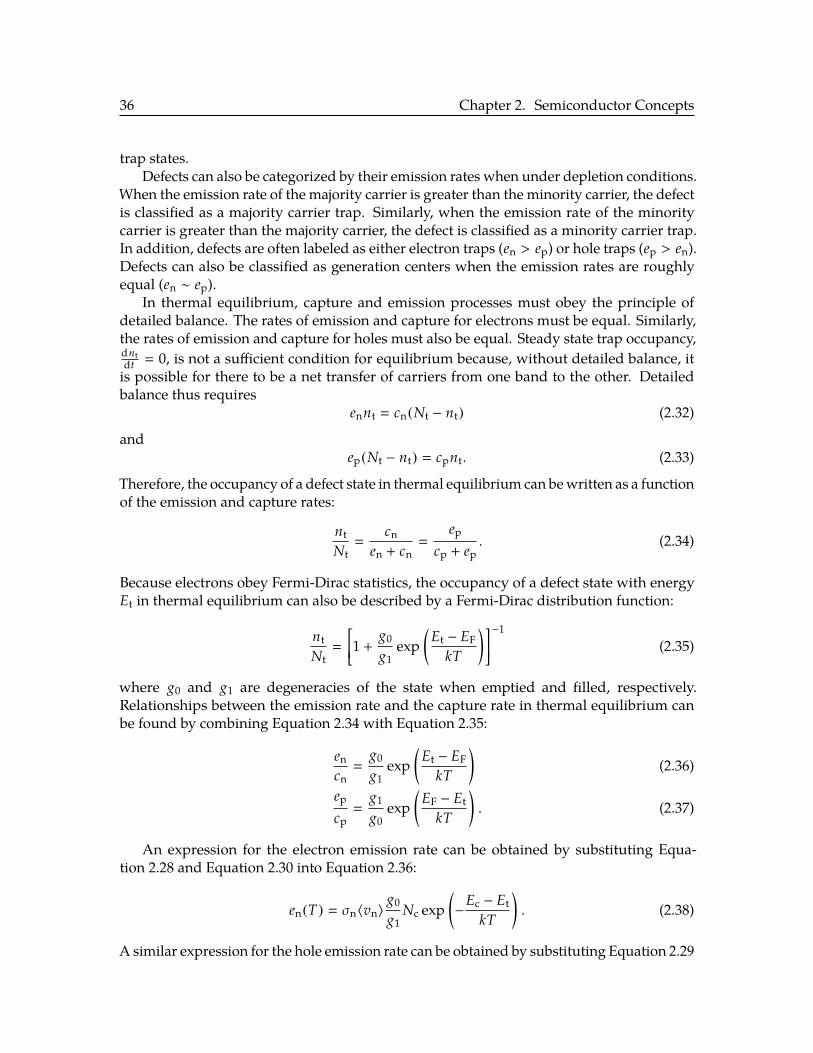
at a defect state (Et) within the bandgap.
where nt is the number of occupied states, Nt is the total concentration of deep states, cn
and cp are the capture rates for electrons and holes, and en and ep are the emission rates for
electrons and holes. The capture rates cn and cp are described by
cn σn〈vn〉n , (2.28)
cp σp〈vp〉p. (2.29)
Electron and hole concentrations for non-degenerate semiconductors are
n Nc exp
(−
Ec − EF
kT
)(2.30)
p Nv exp
(−
EF − Ev
kT
)(2.31)
where Nc is the effective density of states in the conduction band, Nv is the effective density
of states in the valence band, Ec is the conduction band edge, Ev is the valence band edge,
and EF is the Fermi level.
The relative magnitudes of capture rates can be used to categorize defect states. If the
capture rate for one carrier type is much larger than for the other type, then the defect can
be classified as a trap state. If instead they are both large and of comparable magnitude,
then the defect can be classified as a recombination center. However, a specific defect
state could be classified as both a trap state and recombination state depending on the
carrier concentrations. When a defect state is located within the depletion region of a diode,
regardless of the magnitude of the capture cross section, the capture rates are very small
due to low carrier concentrations. In that situation, all defect states could be classified as
36 Chapter 2. Semiconductor Concepts
trap states.
Defects can also be categorized by their emission rates when under depletion conditions.
When the emission rate of the majority carrier is greater than the minority carrier, the defect
is classified as a majority carrier trap. Similarly, when the emission rate of the minority
carrier is greater than the majority carrier, the defect is classified as a minority carrier trap.
In addition, defects are often labeled as either electron traps (en > ep) or hole traps (ep > en).
Defects can also be classified as generation centers when the emission rates are roughly
equal (en ∼ ep).
In thermal equilibrium, capture and emission processes must obey the principle of
detailed balance. The rates of emission and capture for electrons must be equal. Similarly,
the rates of emission and capture for holes must also be equal. Steady state trap occupancy,
dnt
dt 0, is not a sufficient condition for equilibrium because, without detailed balance, it
is possible for there to be a net transfer of carriers from one band to the other. Detailed
balance thus requires
ennt cn(Nt − nt) (2.32)
and
ep(Nt − nt) cpnt. (2.33)
Therefore, the occupancy of a defect state in thermal equilibrium can be written as a function
of the emission and capture rates:
nt
Nt
cn
en + cn
ep
cp + ep
. (2.34)
Because electrons obey Fermi-Dirac statistics, the occupancy of a defect state with energy
Et in thermal equilibrium can also be described by a Fermi-Dirac distribution function:
nt
Nt
1 +
g0
g1
exp
(Et − EF
kT
)
−1
(2.35)
where g0 and g1 are degeneracies of the state when emptied and filled, respectively.
Relationships between the emission rate and the capture rate in thermal equilibrium can
be found by combining Equation 2.34 with Equation 2.35:
en
cn
g0
g1
exp
(Et − EF
kT
)(2.36)
ep
cp
g1
g0
exp
(EF − Et
kT
). (2.37)
An expression for the electron emission rate can be obtained by substituting Equa-
tion 2.28 and Equation 2.30 into Equation 2.36:
en(T) σn〈vn〉g0
g1
Nc exp
(−
Ec − Et
kT
). (2.38)
A similar expression for the hole emission rate can be obtained by substituting Equation 2.29
2.3. Dynamic Behavior of Deep Defect States 37
and Equation 2.31 into Equation 2.37:
ep(T) σp〈vp〉g1
g0
Nv exp
(−
Et − Ev
kT
). (2.39)
We can see that for trap states located in the upper half of the bandgap, en > ep, and for
states in the lower half of the bandgap, ep > en. Therefore, for an n-type material, majority
carrier traps will be observed in the upper half of the bandgap while minority carrier traps
will be observed in the lower half of the bandgap.
2.3.1 Impact of Defect States on Device Performance
As previously mentioned, defect states in the bandgap act as capture and emission centers
for carriers. This primarily has two effects in semiconductors which can drastically affect
the performance of electronic and optoelectronic devices:
1. Carrier Compensation
2. Carrier Generation-Recombination
Carrier compensation refers to a reduction in the free carrier concentration due to the
presence of defect states. Typically, this is related to the capture of majority carriers (by
deep states) or generation of minority carriers (by shallow states). In addition, free carrier
concentrations can be compensated by formation of defect associates containing dopant
atoms (e.g. vacancy binding with a phosphorus dopant atom) which are not ionized at
room temperature. Because the resistivity, ρ, is related to carrier concentrations by
ρ 1
q(µnn + µpp)(2.40)
where µn and µp are the mobilities for electrons and holes respectively, carrier compensation
primarily has the effect of increasing the resistivity which can lead to a variety of issues in
devices (e.g., increased RC delay, energy losses). However, intentional compensation via
defect states can also be useful for applications requiring high resistivity material such as
photoconductors. This can be achieved through addition of impurities and/or irradiation
of the material. In most applications, carrier compensation is not an issue due to the high
level of control of impurities in semiconductors. Because carriers are compensated by only
one or two carriers per defect, impurities must be present in concentrations close to the
dopant concentration to drastically alter the resistivity.
However, as previously mentioned, defect states can also mediate generation and
recombination (through SRH processes) which can significantly alter carrier lifetimes even
in below parts per billion defect concentrations. Defect states are particularly deleterious
for optoelectronic applications which are all minority carrier devices. For a few specific
applications, recombination and generation due to defect states largely results in the
following:
• Photodiodes: The noise level and power dissipation is determined by the dark
current (leakage current) due to diffusion of thermally generated minority carriers to

38 Chapter 2. Semiconductor Concepts
the junction. Defects which generate states near mid-gap can drastically lower the
energy required to thermally generate carriers thus drastically increasing the dark
current thereby decreasing signal/noise and increasing power consumption.
• Light Sources: Defect states increase competition of non-radiative recombination
with radiative recombination lowering the quantum efficiency of emission. As we
will discuss in further detail in Chapter 4, this can also lead to increased threshold
currents for lasers.
• Photovoltaics: Electron-hole pairs generated in the depletion region of a photovoltaic
cell are split by the junction and efficiently collected. In order for carriers generated
outside of the depletion region to provide useful energy, minority carriers must diffuse
to the junction before recombination. When defect states reduce carrier lifetimes, a
larger fraction of carriers will recombination before diffusing to the junction thereby
lowering the efficiency of cell.
Similar to carrier compensation, for some applications, it is desirable to reduce carrier
lifetimes (e.g., high speed electronics) and impurities which introduce mid-gap states are
intentionally added. It should be noted that this section only contains brief descriptions for
some of the numerous effects that defect states have on semiconductor devices.

Chapter 3
Point Defects in Germanium
High carrier mobilities, compatibility with silicon processes, and a direct bandgap corre-
sponding to a wavelength of 1.55 µm make germanium a strong candidate for the new
generation of MOSFETs and as the active material in a variety of optoelectronic devices
including photodetectors [17, 18] , modulators [19–21], and light sources (Chapter 4). How-
ever, the properties of point defects in germanium have not been investigated as thoroughly
as those of silicon. This is partially a consequence of the limited success of electron para-
magnetic resonance (EPR) studies in germanium due to its varied isotopic composition4
and large spin orbit coupling which yields a short spin-lattice relaxation time [22, 23]. In
addition, knowledge of defects in silicon is not directly applicable to germanium, as was
shown in SixGe1-x studies [24]. EPR currently does not provide direct identification of
defects in germanium; therefore, identifications must be obtained through more indirect
methods. In this work, we use60
Co gamma, alpha, and neutron irradiation to generate
vacancy and interstitial related defect associates in Sb-doped germanium which we char-
acterize by deep-level transient spectroscopy (DLTS). Similar DLTS studies of defects in
germanium have been performed in the past [25–33], however, as is often noted, there is
little consensus and considerable scatter between different studies as to the properties and
identification of previously observed defects. In conjunction with the analysis of defect
state properties by DLTS, annealing studies were also performed to investigate the kinetics
of various defect growth and decay reactions. Electronic characterization (from DLTS)
together with the reaction kinetics are analyzed in order to make tentative assignments for
the identity of some defect states.
3.1 Deep Level Transient Spectrocopy (DLTS)Deep level transient spectroscopy (DLTS) is a technique for the characterization of electrically-
active defect states developed in 1974 by Lang [34]. Using DLTS, defect state concentrations,
energy levels, and capture cross sections can be measured giving complete characteri-
zation of the defect properties which ultimately affect device performance. In addition,
compared to other analytical techniques, such as fourier transform infrared spectroscopy
The work in this chapter is partially adapted from [16] and was done in collaboration with C. Monmeyran, also
a member of the Kimerling group at MIT.

40 Chapter 3. Point Defects in Germanium
(FTIR) and secondary ion mass spectroscopy (SIMS), DLTS has greater sensitivity to defect
concentration. The detection limit for defect concentrations is ∼10−5
times the free carrier
concentration allowing for measurement of defect concentrations as low as 109
cm−3
to
1010
cm−3
in this work. The remainder of Section 3.1 contains an introduction to the theory
and application of DLTS for the characterization of defect states in n-type material. For
brevity and clarity, expressions relevant to the analysis of p-type materials will be omitted,
however a similar process can be used to characterize defects in p-type materials via DLTS.
More detailed descriptions of DLTS techniques can be found in a review by Miller et al. [35]
and a book by Blood et al. [10].
3.1.1 Theory of Operation
Using DLTS, defects are characterized by observation of thermal emission of carriers from
deep states within the depletion region of a diode by means of a capacitive transient.
Emission of majority carriers from trap states increases the net positive space charge density
in the depletion region of a semiconductor junction. If the diode is kept at constant voltage,
the depletion region shrinks in response to the additional charge resulting in a measurable
increase in the junction capacitance.
Schematics for an n-type Schottky diode under neutral and reverse biased conditions
are shown in Figure 3-1. In the absence of a bias, trap states are occupied outside the
depletion width x0 because EF > Et which leads to cn > en (Equation 2.36). When a reverse
bias is applied, electrons are depleted for an extended distance xd from the surface. The
removal of free electrons halts the capture process and traps empty by thermal emission of
electrons at a rate en described by Equation 2.38. This produces an exponential transient in
the capacitance measured across the junction which can be described by
C(t) C(∞) + ∆C exp(−ent) (3.1)
where C(∞) is the steady state capacitance at reverse bias and ∆C is the difference in
capacitance due to the emptying of traps which can be related to the concentration of trap
states (Section 3.1.3.2).
During a DLTS measurement, the following voltage biasing steps are repeated to
generate capacitance transients which correspond to thermal emission of carriers from
traps (Figure 3-2):
1. The diode is held in reverse bias which sweeps carriers out of the depletion region
and empties traps.
2. The diode is pulsed forward which reduces the depletion region and fills traps with
carriers.
3. The diode is put back into reverse bias after the pulse. Free carriers are swept out of
the depletion region and capture of carriers by traps is halted.
4. Capacitance transient is observed as traps empty due to thermal emission of carriers.
Often an observed capacitance transient contains contributions from several defects, each
with different emission rates. This simplest way to separate out distinct defects is to construct
a DLTS spectrum through the application of a rate window to the capacitance transients
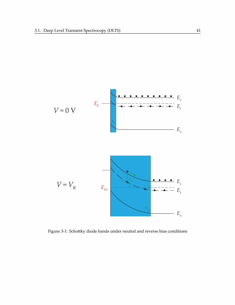
3.1. Deep Level Transient Spectrocopy (DLTS) 41
EcEF
Ev
Et
Ec
Ev
Et
en
xd
x0
EFn
V = 0 V
V = VR
Figure 3-1: Schottky diode bands under neutral and reverse bias conditions
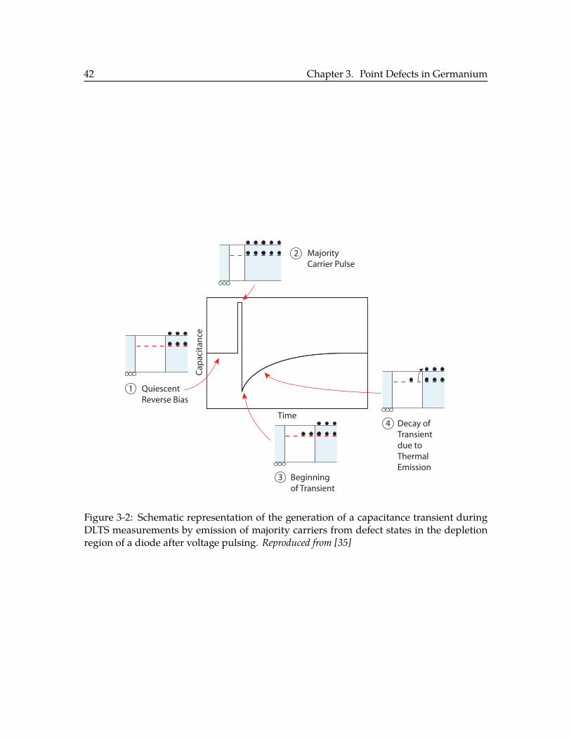
42 Chapter 3. Point Defects in Germanium
Time
QuiescentReverse Bias
MajorityCarrier Pulse
Beginningof Transient
Decay ofTransientdue toThermalEmission
1
2
3
4
Figure 3-2: Schematic representation of the generation of a capacitance transient during
DLTS measurements by emission of majority carriers from defect states in the depletion
region of a diode after voltage pulsing. Reproduced from [35]
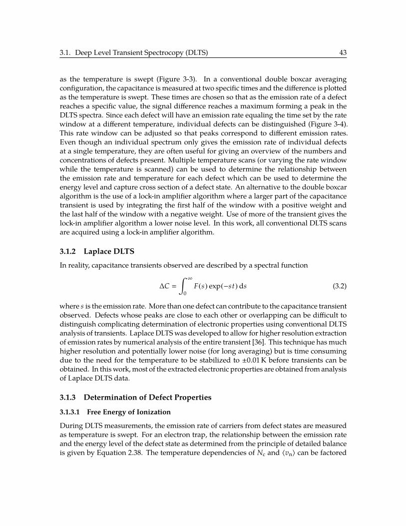
3.1. Deep Level Transient Spectrocopy (DLTS) 43
as the temperature is swept (Figure 3-3). In a conventional double boxcar averaging
configuration, the capacitance is measured at two specific times and the difference is plotted
as the temperature is swept. These times are chosen so that as the emission rate of a defect
reaches a specific value, the signal difference reaches a maximum forming a peak in the
DLTS spectra. Since each defect will have an emission rate equaling the time set by the rate
window at a different temperature, individual defects can be distinguished (Figure 3-4).
This rate window can be adjusted so that peaks correspond to different emission rates.
Even though an individual spectrum only gives the emission rate of individual defects
at a single temperature, they are often useful for giving an overview of the numbers and
concentrations of defects present. Multiple temperature scans (or varying the rate window
while the temperature is scanned) can be used to determine the relationship between
the emission rate and temperature for each defect which can be used to determine the
energy level and capture cross section of a defect state. An alternative to the double boxcar
algorithm is the use of a lock-in amplifier algorithm where a larger part of the capacitance
transient is used by integrating the first half of the window with a positive weight and
the last half of the window with a negative weight. Use of more of the transient gives the
lock-in amplifier algorithm a lower noise level. In this work, all conventional DLTS scans
are acquired using a lock-in amplifier algorithm.
3.1.2 Laplace DLTS
In reality, capacitance transients observed are described by a spectral function
∆C
∫∞
0
F(s) exp(−st) ds (3.2)
where s is the emission rate. More than one defect can contribute to the capacitance transient
observed. Defects whose peaks are close to each other or overlapping can be difficult to
distinguish complicating determination of electronic properties using conventional DLTS
analysis of transients. Laplace DLTS was developed to allow for higher resolution extraction
of emission rates by numerical analysis of the entire transient [36]. This technique has much
higher resolution and potentially lower noise (for long averaging) but is time consuming
due to the need for the temperature to be stabilized to ±0.01 K before transients can be
obtained. In this work, most of the extracted electronic properties are obtained from analysis
of Laplace DLTS data.
3.1.3 Determination of Defect Properties
3.1.3.1 Free Energy of Ionization
During DLTS measurements, the emission rate of carriers from defect states are measured
as temperature is swept. For an electron trap, the relationship between the emission rate
and the energy level of the defect state as determined from the principle of detailed balance
is given by Equation 2.38. The temperature dependencies of Nc and 〈vn〉 can be factored

44 Chapter 3. Point Defects in Germanium
0 t1 t2Time
Capa
cita
nce
Tran
sien
ts a
t Var
ious
Tem
pera
ture
s
Tem
pera
ture
C(t2) − C(t1)
Figure 3-3: Construction of a DLTS spectrum by implementation of a rate window using a
double boxcar configuration. Reproduced from [35]
3.1. Deep Level Transient Spectrocopy (DLTS) 45
AdjustableRate Window
1 / T
1 / T
DLT
S Si
gn
alLo
g(T
her
mal
Em
issi
on
Rat
e)
Figure 3-4: Schematic illustrating how a rate window produces a peak in the DLTS spectrum
when the emission rate of the defect state corresponds to the chosen rate window. Reproducedfrom [35]
46 Chapter 3. Point Defects in Germanium
out to yield the following expression:
en
T2
Aσ exp
(−
Ec − Et
kT
)(3.3)
where A is independent of temperature and contains the relevant physical and material
constants. Often the defect level and capture cross section are simply determined from
the slope and y-intercept of a plot of en/T2vs. 1/T. This results in an intrinsically
rough estimation for the capture cross section due to the imprecision of the y-intercept
extrapolation on an Arrhenius plot. This method can yield values that are significantly
different from the real values due to the fact that the defect level and capture cross sections
can be temperature dependent. In addition, the free energy of ionization of the defect
contains enthalpy and entropy contributions. The capture process can be thermally activated
resulting in an Arrhenius temperature dependence for the capture cross section. These two
facts yield a difference between the measured (apparent) and real enthalpy of ionization
and capture cross section. Consequently, for an accurate determination of defect properties
the following expressions should be considered:
Ec − Et ∆G ∆H − T∆S (3.4)
and
σ(T) σ∞ exp
(−
EσkT
). (3.5)
Thus,
en
T2
Aσ∞ exp
(∆Sk
)exp
(−∆H + Eσ
kT
). (3.6)
Therefore instead of directly determining real values, an analysis of the plot of en/T2
vs. 1/T leads to the extraction of an apparent enthalpy, Ea, and apparent cross section, σa,
which correspond to
Ea ∆H + Eσ (3.7)
and
σa σ∞ exp
(∆Sk
). (3.8)
Pulse filling methods (Section 3.1.3.3) can be used to independently measure the real capture
cross section, σ(T). Once Eσ and σ∞ are known, the enthalpy and entropy can be calculated
allowing for precise determination of the energy level of the defect state.
3.1.3.2 Defect Concentration
In addition to determination of the activation energy and capture cross section, DLTS allows
for calculation of the defect concentration from
Nt ≈ 2Nd
∆CCR
(3.9)

3.1. Deep Level Transient Spectrocopy (DLTS) 47
where Nd is the donor dopant concentration, ∆C is the magnitude of the capacitance
transient, and CR is the capacitance at reverse bias. This equation is convenient because the
concentration measurement does not rely on the location of the defect energy level within
the bandgap. However, this calculation can be off by more than 50 % when the defect level
is far from the Fermi level. In that case, there is a significant area, known as the transition
region (Figure 3-5), between the depletion region and the neutral bulk of the material which
contains carriers that have not been swept out of the depletion region due to screening
effects [37]. If the precise energy level of the trap has been determined then the width of
the transition region can be determined from
λ
√2ε(EF − Et)
q2Nd
(3.10)
where ε is the dielectric constant, EF is the Fermi level, Et is the free energy of the trap,
and q is the elementary charge constant. With knowledge of the transition region width,
diode area, A, and the junction capacitance under filling conditions, CP, the precise defect
concentration can be calculated from
Nt 2Nd
∆CCR
1 −
(CR
CP
)2
−2λCR
εA
(1 −
CR
CP
)
−1
. (3.11)
Ec
Ev
EtEFn
xd
λ
Figure 3-5: Schematic diagram of transition region for a reverse biased Schottky diode
containing deep defect states.
48 Chapter 3. Point Defects in Germanium
3.1.3.3 Real Capture Cross Section
The real capture cross section can be determined by varying the duration of the DLTS filling
pulse and observing how the magnitude of the DLTS signal varies in response. For defects
observed in n-type materials, en ep and cp is negligible, whereas in p-type materials,
ep en and cn is negligible. In addition, for short durations, majority carrier emission can
be neglected reducing Equation 2.27 to
dnt
dt cn(Nt − nt), n-type (3.12)
dnt
dt −cpnt. p-type (3.13)
Assuming nt(0) 0 for majority carrier n-type traps and nt(0) Nt for majority carrier
p-type traps, these equations can be solved to yield
nt(t) Nt
[1 − exp(−cnt)
], n-type (3.14)
nt(t) Nt exp(−cpt). p-type (3.15)
To represent the number of emptied states due to hole capture, Equation 3.15 can be
rewritten as
Nt − nt(t) Nt
[1 − exp(−cpt)
]. (3.16)
In a typical DLTS measurement, τp, the filling pulse duration, is chosen such that cn,pτp 1
and the trap is either completely filled with electrons for n-type materials, nt(τp) Nt, or
completely emptied of electrons for p-type materials, nt(τp) 0. However, for short filling
pulses, the measured DLTS signal (Equation 3.1) is modified:
∆C(τp) [1 − exp(−cn,pτp)
]∆Cmax (3.17)
where ∆Cmax is the maximum observed signal obtained when τp is long. This expression
allows for experimental measurement of the capture rate from DLTS measurements with
varying filling pulse durations. The real capture cross section can then be determined from
Equation 2.28 for electron traps and Equation 2.29 for hole traps. Measurements can be
repeated at various temperatures to determine the temperature dependence of the capture
cross section in order to extract out the parameters (σ∞ and Eσ) in Equation 3.5.
It should be noted that if the capture cross section is too large, then measurement
becomes limited by the inability to generate well-shaped pulses with durations short
enough to only partially fill traps. In our experimental setup (Figure 3-6), the filling pulse
duration is limited to ∼200 ns.
3.1.4 Experimental Apparatus
A schematic of the experimental apparatus used for DLTS measurements is shown in
Figure 3-6. Samples are mounted within a cryostat with electrical connections allowing for
measurement of capacitance transients as the sample is cooled or heated. During sample
pulsing, we utilized an analog switch in order to alternately connect the diode sample to
the pulse generator and capacitance meter. If the capacitance meter is not removed from
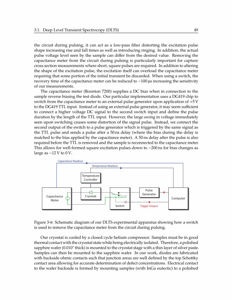
3.1. Deep Level Transient Spectrocopy (DLTS) 49
the circuit during pulsing, it can act as a low-pass filter distorting the excitation pulse
shape increasing rise and fall times as well as introducing ringing. In addition, the actual
pulse voltage level seen by the sample can differ from the desired value. Removing the
capacitance meter from the circuit during pulsing is particularly important for capture
cross section measurements where short, square pulses are required. In addition to altering
the shape of the excitation pulse, the excitation itself can overload the capacitance meter
requiring that some portion of the initial transient be discarded. When using a switch, the
recovery time of the capacitance meter can be reduced to ∼100 µs increasing the sensitivity
of our measurements.
The capacitance meter (Boonton 7200) supplies a DC bias when in connection to the
sample reverse biasing the test diode. Our particular implementation uses a DG419 chip to
switch from the capacitance meter to an external pulse generator upon application of +5 V
to the DG419 TTL input. Instead of using an external pulse generator, it may seem sufficient
to connect a higher voltage DC signal to the second switch input and define the pulse
duration by the length of the TTL input. However, the large swing in voltage immediately
seen upon switching causes some distortion of the signal pulse. Instead, we connect the
second output of the switch to a pulse generator which is triggered by the same signal as
the TTL pulse and sends a pulse after a 50 ns delay (where the bias during the delay is
matched to the bias applied by the capacitance meter). A 50 ns delay after the pulse is also
required before the TTL is removed and the sample is reconnected to the capacitance meter.
This allows for well-formed square excitation pulses down to ∼200 ns for bias changes as
large as −12 V to 0 V.
Figure 3-6: Schematic diagram of our DLTS experimental apparatus showing how a switch
is used to remove the capacitance meter from the circuit during pulsing.
Our cryostat is cooled by a closed cycle helium compressor. Samples must be in good
thermal contact with the cryostat state while being electrically isolated. Therefore, a polished
sapphire wafer (0.010" thick) is mounted to the cryostat stage with a thin layer of silver paste.
Samples can then be mounted to the sapphire wafer. In our work, diodes are fabricated
with backside ohmic contacts such that junction areas are well defined by the top Schottky
contact area allowing for accurate determination of defect concentrations. Electrical contact
to the wafer backside is formed by mounting samples (with InGa eutectic) to a polished
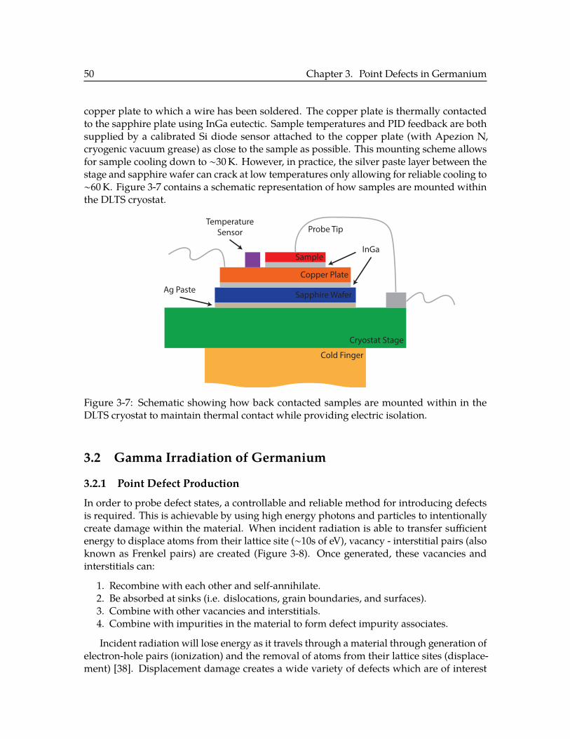
50 Chapter 3. Point Defects in Germanium
copper plate to which a wire has been soldered. The copper plate is thermally contacted
to the sapphire plate using InGa eutectic. Sample temperatures and PID feedback are both
supplied by a calibrated Si diode sensor attached to the copper plate (with Apezion N,
cryogenic vacuum grease) as close to the sample as possible. This mounting scheme allows
for sample cooling down to ∼30 K. However, in practice, the silver paste layer between the
stage and sapphire wafer can crack at low temperatures only allowing for reliable cooling to
∼60 K. Figure 3-7 contains a schematic representation of how samples are mounted within
the DLTS cryostat.
Sample
Cold Finger
Cryostat Stage
Copper Plate
Sapphire Wafer
TemperatureSensor Probe Tip
InGa
Ag Paste
Figure 3-7: Schematic showing how back contacted samples are mounted within in the
DLTS cryostat to maintain thermal contact while providing electric isolation.
3.2 Gamma Irradiation of Germanium
3.2.1 Point Defect Production
In order to probe defect states, a controllable and reliable method for introducing defects
is required. This is achievable by using high energy photons and particles to intentionally
create damage within the material. When incident radiation is able to transfer sufficient
energy to displace atoms from their lattice site (∼10s of eV), vacancy - interstitial pairs (also
known as Frenkel pairs) are created (Figure 3-8). Once generated, these vacancies and
interstitials can:
1. Recombine with each other and self-annihilate.
2. Be absorbed at sinks (i.e. dislocations, grain boundaries, and surfaces).
3. Combine with other vacancies and interstitials.
4. Combine with impurities in the material to form defect impurity associates.
Incident radiation will lose energy as it travels through a material through generation of
electron-hole pairs (ionization) and the removal of atoms from their lattice sites (displace-
ment) [38]. Displacement damage creates a wide variety of defects which are of interest
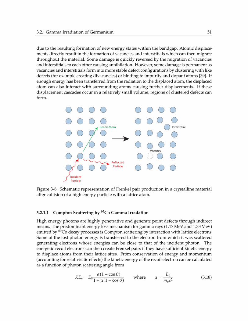
3.2. Gamma Irradiation of Germanium 51
due to the resulting formation of new energy states within the bandgap. Atomic displace-
ments directly result in the formation of vacancies and interstitials which can then migrate
throughout the material. Some damage is quickly reversed by the migration of vacancies
and interstitials to each other causing annihilation. However, some damage is permanent as
vacancies and interstitials form into more stable defect configurations by clustering with like
defects (for example creating divacancies) or binding to impurity and dopant atoms [39]. If
enough energy has been transferred from the radiation to the displaced atom, the displaced
atom can also interact with surrounding atoms causing further displacements. If these
displacement cascades occur in a relatively small volume, regions of clustered defects can
form.
IncidentParticle
ReectedParticle
Recoil Atom
Vacancy
Interstitial
Figure 3-8: Schematic representation of Frenkel pair production in a crystalline material
after collision of a high energy particle with a lattice atom.
3.2.1.1 Compton Scattering by 60Co Gamma Irradation
High energy photons are highly penetrative and generate point defects through indirect
means. The predominant energy loss mechanism for gamma rays (1.17 MeV and 1.33 MeV)
emitted by60
Co decay processes is Compton scattering by interaction with lattice electrons.
Some of the lost photon energy is transferred to the electron from which it was scattered
generating electrons whose energies can be close to that of the incident photon. The
energetic recoil electrons can then create Frenkel pairs if they have sufficient kinetic energy
to displace atoms from their lattice sites. From conservation of energy and momentum
(accounting for relativisitic effects) the kinetic energy of the recoil electron can be calculated
as a function of photon scattering angle from
KEe E0
α(1 − cos θ)1 + α(1 − cos θ)
where α E0
mec2
(3.18)
52 Chapter 3. Point Defects in Germanium
where E0 is the energy of the incident photon and θ is the scattering angle. The differential
cross section for photons scattered by electrons can be calculated from the Klein-Nishina
formula [40]:
dσKN
dΩ(α, θ)
r2
0
2
1
(1 + α(1 − cos θ))2
(1 + cos
2 θ +α2(1 − cos θ)2
1 + α(1 − cos θ)
)(3.19)
whereΩ is the solid angle and r0 is the classical radius of an electron. Using this expression
we can find the probability that a photon will be scattered between 0 and θ:
P(0→ θ)
∫ θ
0
dσKN
dΩdΩ∫ π
0
dσKN
dΩdΩ
. (3.20)
The probability that a photon will be scattered between two angles (θ1 and θ2) is then
P(θ1 → θ2) P(0→ θ2) − P(0→ θ1). (3.21)
Figure 3-9 shows plots of scattering probability and kinetic energy transferred as a
function of scattering angle for Compton scattering of incident photons with 1.33 MeV.
The kinetic energy of the Compton electron can take any value between 0 and 1.1 MeV
for irradiation by photons generated from60
Co decay. Figure 3-10 shows the probability
density of scattering as a function of electron energy after Compton scattering of a 1.33 MeV
photon.
3.2.1.2 Number of Displacements Generated per Collision
The maximum energy transferred to a lattice atom after a binary collision with a high kinetic
energy electron (accounting for relativistic effects) can be found from
Tmax 2ME(E + 2mec2)
(me + M)2c2 + 2ME(3.22)
where me is the mass of an electron, M is the mass of the lattice atom, and E is the energy
of the incident electron. The maximum energy transferred to Si and Ge atoms from recoil
electrons produced by Compton scattering of60
Co gamma irradiation is plotted in Figure 3-
11. Previous studies [41] have shown that to create one Frenkel pair, the transferred energy
needs to be above a threshold of approximately 20 eV. In order to create two Frenkel pairs
from a single collision, the transferred energy needs to be four times the value necessary for
single Frenkel pair production according to the Kinchin-Pease model [42]. As observed in
Figure 3-11, the formation of two Frenkel pairs by one scattered electron is possible in silicon
but not in germanium. Therefore, the divacancy, the defect with the largest introduction
rate in irradiated CZ silicon after the A-center (V-O pair), can be created as a primary defect
in silicon but not germanium.
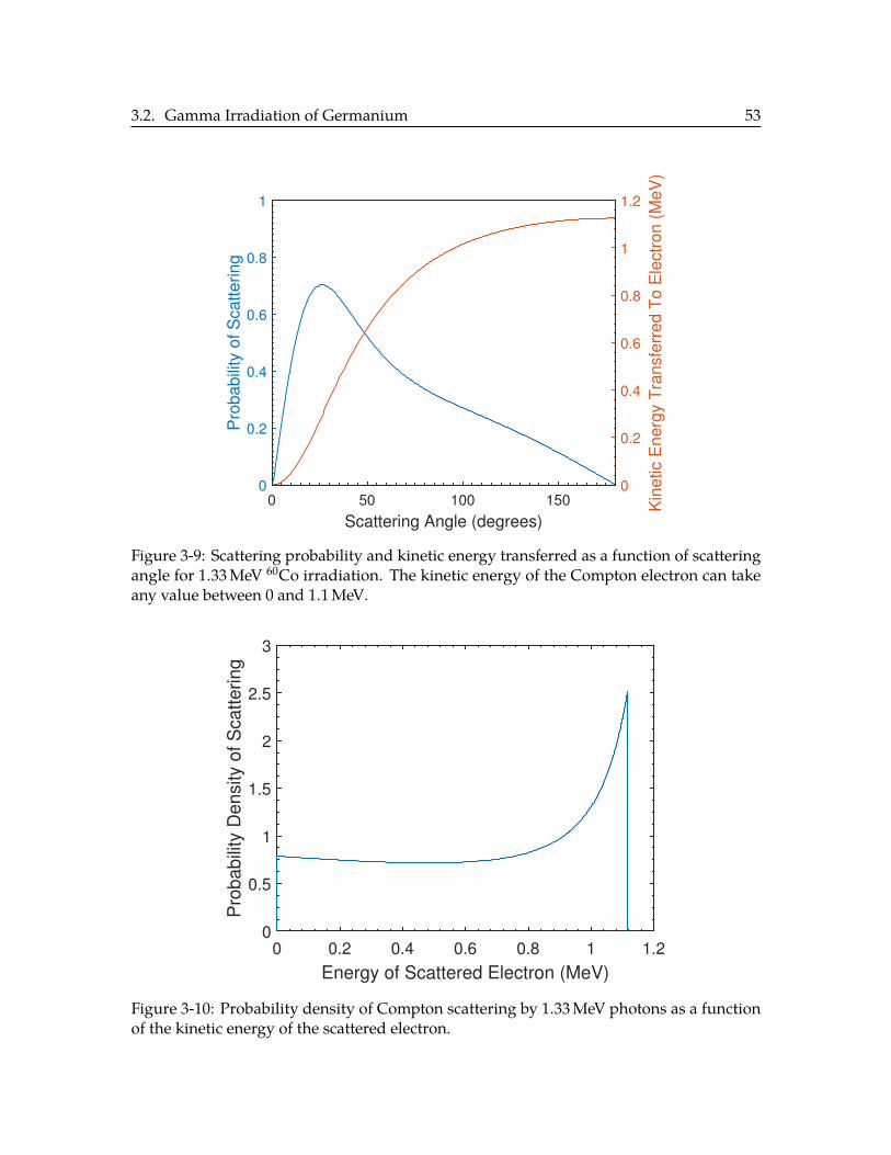
3.2. Gamma Irradiation of Germanium 53
Scattering Angle (degrees)
0 50 100 150
Pro
babili
ty o
f S
ca
ttering
0
0.2
0.4
0.6
0.8
1
Kin
etic E
ne
rgy T
ransfe
rred
To
Ele
ctr
on (
MeV
)
0
0.2
0.4
0.6
0.8
1
1.2
Figure 3-9: Scattering probability and kinetic energy transferred as a function of scattering
angle for 1.33 MeV60
Co irradiation. The kinetic energy of the Compton electron can take
any value between 0 and 1.1 MeV.
Energy of Scattered Electron (MeV)
0 0.2 0.4 0.6 0.8 1 1.2
Pro
ba
bili
ty D
en
sity o
f S
ca
tte
rin
g
0
0.5
1
1.5
2
2.5
3
Figure 3-10: Probability density of Compton scattering by 1.33 MeV photons as a function
of the kinetic energy of the scattered electron.
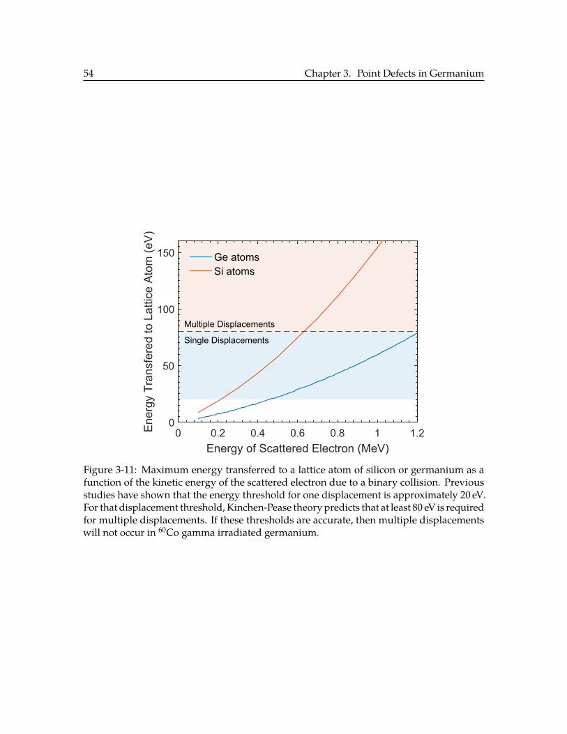
54 Chapter 3. Point Defects in Germanium
Energy of Scattered Electron (MeV)
0 0.2 0.4 0.6 0.8 1 1.2Energ
y T
ransfe
red to L
attic
e A
tom
(eV
)
0
50
100
150
Single Displacements
Multiple Displacements
Ge atoms
Si atoms
Figure 3-11: Maximum energy transferred to a lattice atom of silicon or germanium as a
function of the kinetic energy of the scattered electron due to a binary collision. Previous
studies have shown that the energy threshold for one displacement is approximately 20 eV.
For that displacement threshold, Kinchen-Pease theory predicts that at least 80 eV is required
for multiple displacements. If these thresholds are accurate, then multiple displacements
will not occur in60
Co gamma irradiated germanium.
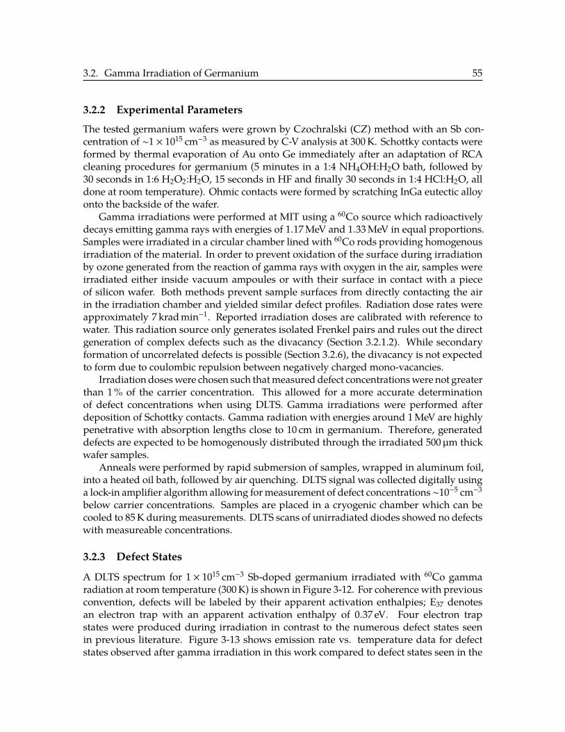
3.2. Gamma Irradiation of Germanium 55
3.2.2 Experimental Parameters
The tested germanium wafers were grown by Czochralski (CZ) method with an Sb con-
centration of ∼1 × 10¹⁵
cm−3
as measured by C-V analysis at 300 K. Schottky contacts were
formed by thermal evaporation of Au onto Ge immediately after an adaptation of RCA
cleaning procedures for germanium (5 minutes in a 1:4 NH4OH:H2O bath, followed by
30 seconds in 1:6 H2O2:H2O, 15 seconds in HF and finally 30 seconds in 1:4 HCl:H2O, all
done at room temperature). Ohmic contacts were formed by scratching InGa eutectic alloy
onto the backside of the wafer.
Gamma irradiations were performed at MIT using a60
Co source which radioactively
decays emitting gamma rays with energies of 1.17 MeV and 1.33 MeV in equal proportions.
Samples were irradiated in a circular chamber lined with60
Co rods providing homogenous
irradiation of the material. In order to prevent oxidation of the surface during irradiation
by ozone generated from the reaction of gamma rays with oxygen in the air, samples were
irradiated either inside vacuum ampoules or with their surface in contact with a piece
of silicon wafer. Both methods prevent sample surfaces from directly contacting the air
in the irradiation chamber and yielded similar defect profiles. Radiation dose rates were
approximately 7 krad min−1
. Reported irradiation doses are calibrated with reference to
water. This radiation source only generates isolated Frenkel pairs and rules out the direct
generation of complex defects such as the divacancy (Section 3.2.1.2). While secondary
formation of uncorrelated defects is possible (Section 3.2.6), the divacancy is not expected
to form due to coulombic repulsion between negatively charged mono-vacancies.
Irradiation doses were chosen such that measured defect concentrations were not greater
than 1 % of the carrier concentration. This allowed for a more accurate determination
of defect concentrations when using DLTS. Gamma irradiations were performed after
deposition of Schottky contacts. Gamma radiation with energies around 1 MeV are highly
penetrative with absorption lengths close to 10 cm in germanium. Therefore, generated
defects are expected to be homogenously distributed through the irradiated 500 µm thick
wafer samples.
Anneals were performed by rapid submersion of samples, wrapped in aluminum foil,
into a heated oil bath, followed by air quenching. DLTS signal was collected digitally using
a lock-in amplifier algorithm allowing for measurement of defect concentrations∼10−5
cm−3
below carrier concentrations. Samples are placed in a cryogenic chamber which can be
cooled to 85 K during measurements. DLTS scans of unirradiated diodes showed no defects
with measureable concentrations.
3.2.3 Defect States
A DLTS spectrum for 1 × 10¹⁵
cm−3
Sb-doped germanium irradiated with60
Co gamma
radiation at room temperature (300 K) is shown in Figure 3-12. For coherence with previous
convention, defects will be labeled by their apparent activation enthalpies; E37 denotes
an electron trap with an apparent activation enthalpy of 0.37 eV. Four electron trap
states were produced during irradiation in contrast to the numerous defect states seen
in previous literature. Figure 3-13 shows emission rate vs. temperature data for defect
states observed after gamma irradiation in this work compared to defect states seen in the
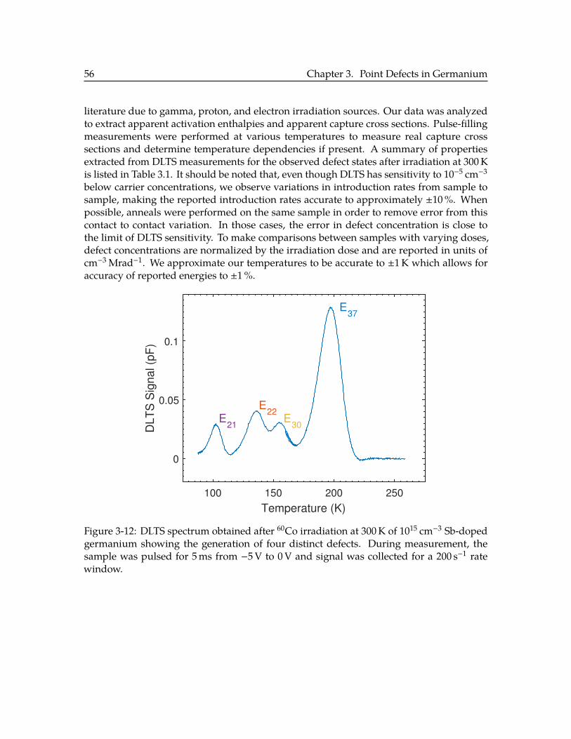
56 Chapter 3. Point Defects in Germanium
literature due to gamma, proton, and electron irradiation sources. Our data was analyzed
to extract apparent activation enthalpies and apparent capture cross sections. Pulse-filling
measurements were performed at various temperatures to measure real capture cross
sections and determine temperature dependencies if present. A summary of properties
extracted from DLTS measurements for the observed defect states after irradiation at 300 K
is listed in Table 3.1. It should be noted that, even though DLTS has sensitivity to 10−5
cm−3
below carrier concentrations, we observe variations in introduction rates from sample to
sample, making the reported introduction rates accurate to approximately ±10 %. When
possible, anneals were performed on the same sample in order to remove error from this
contact to contact variation. In those cases, the error in defect concentration is close to
the limit of DLTS sensitivity. To make comparisons between samples with varying doses,
defect concentrations are normalized by the irradiation dose and are reported in units of
cm−3
Mrad−1
. We approximate our temperatures to be accurate to ±1 K which allows for
accuracy of reported energies to ±1 %.
Temperature (K)
100 150 200 250
DLT
S S
ignal (p
F)
0
0.05
0.1
E37
E21
E22
E30
Figure 3-12: DLTS spectrum obtained after60
Co irradiation at 300 K of 1015
cm−3
Sb-doped
germanium showing the generation of four distinct defects. During measurement, the
sample was pulsed for 5 ms from −5 V to 0 V and signal was collected for a 200 s−1
rate
window.
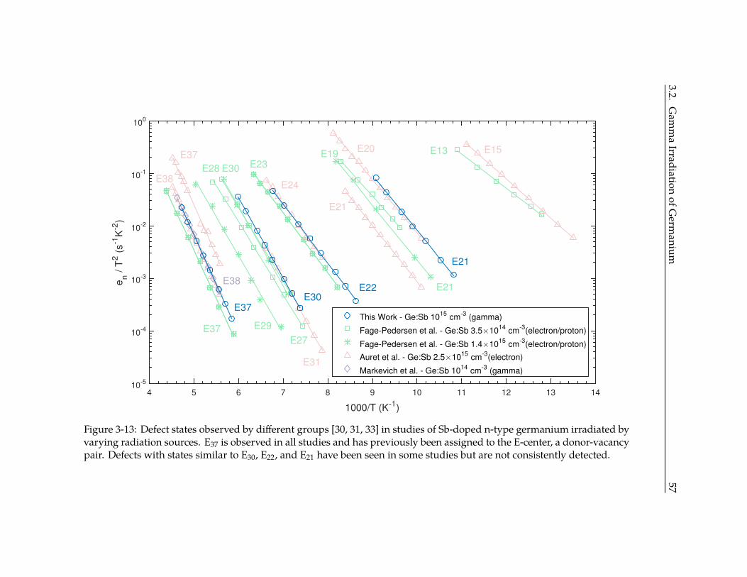
3.2.
Gam
ma
Irrad
iation
of
Germ
an
iu
m57
1000/T (K-1)
4 5 6 7 8 9 10 11 12 13 14
en / T
2 (
s-1
K-2
)
10-5
10-4
10-3
10-2
10-1
100
This Work - Ge:Sb 1015
cm-3
(gamma)
Fage-Pedersen et al. - Ge:Sb 3.5×10¹⁴
cm-3
(electron/proton)
Fage-Pedersen et al. - Ge:Sb 1.4×10¹⁵
cm-3
(electron/proton)
Auret et al. - Ge:Sb 2.5×10¹⁵
cm-3
(electron)
Markevich et al. - Ge:Sb 1014
cm-3
(gamma)
E30E28
E29
E27
E23E19
E21
E13
E38
E37
E31
E24
E20
E21
E15
E37E30
E22
E21
E37
E38
Figure 3-13: Defect states observed by different groups [30, 31, 33] in studies of Sb-doped n-type germanium irradiated by
varying radiation sources. E37 is observed in all studies and has previously been assigned to the E-center, a donor-vacancy
pair. Defects with states similar to E30, E22, and E21 have been seen in some studies but are not consistently detected.

58
Ch
ap
ter
3.
Poin
tD
efects
in
Germ
an
iu
m
Table 3.1: Summary of defect states in60
Co irradiated Sb-doped germanium
Defect
Apparent Enthalpy
(eV)
Free Energy of
Ionization (eV)
Apparent Capture
Cross Section (cm2)
Real Capture Cross
Section (cm2)
Introduction Rate
(cm−3
Mrad−1
)
E370.37 0.29 − 3.94kT 3.9 × 10
−157.6 × 10
−17e−85 meV/kT
2.2 × 10¹¹
E300.30 NA
a1.2 × 10
−14 >10−15
NAb
E220.22 0.22 − 1.53kT 4.6 × 10
−161.1 × 10
−16NA
b
E210.21 0.16 − 8.29kT 8.0 × 10
−142.0 × 10
−17e−54 meV/kT
NAb
aThe experimental apparatus was not fast enough to measure the real capture cross-section of E
30preventing calculation of the real enthalpy and
entropy of ionization.
bNot quantifiable since defect concentrations evolve at 300 K.
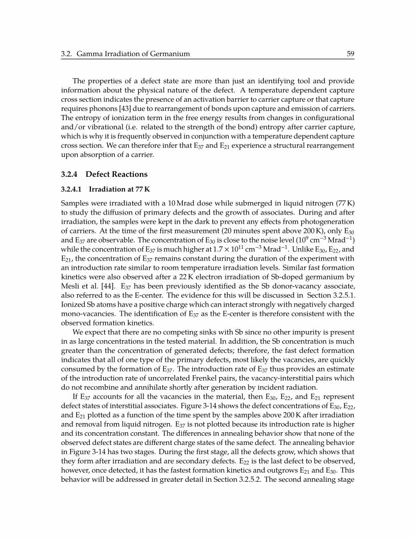
3.2. Gamma Irradiation of Germanium 59
The properties of a defect state are more than just an identifying tool and provide
information about the physical nature of the defect. A temperature dependent capture
cross section indicates the presence of an activation barrier to carrier capture or that capture
requires phonons [43] due to rearrangement of bonds upon capture and emission of carriers.
The entropy of ionization term in the free energy results from changes in configurational
and/or vibrational (i.e. related to the strength of the bond) entropy after carrier capture,
which is why it is frequently observed in conjunction with a temperature dependent capture
cross section. We can therefore infer that E37 and E21 experience a structural rearrangement
upon absorption of a carrier.
3.2.4 Defect Reactions
3.2.4.1 Irradiation at 77 K
Samples were irradiated with a 10 Mrad dose while submerged in liquid nitrogen (77 K)
to study the diffusion of primary defects and the growth of associates. During and after
irradiation, the samples were kept in the dark to prevent any effects from photogeneration
of carriers. At the time of the first measurement (20 minutes spent above 200 K), only E30
and E37 are observable. The concentration of E30 is close to the noise level (109
cm−3
Mrad−1
)
while the concentration of E37 is much higher at 1.7 × 10¹¹
cm−3
Mrad−1
. Unlike E30, E22, and
E21, the concentration of E37 remains constant during the duration of the experiment with
an introduction rate similar to room temperature irradiation levels. Similar fast formation
kinetics were also observed after a 22 K electron irradiation of Sb-doped germanium by
Mesli et al. [44]. E37 has been previously identified as the Sb donor-vacancy associate,
also referred to as the E-center. The evidence for this will be discussed in Section 3.2.5.1.
Ionized Sb atoms have a positive charge which can interact strongly with negatively charged
mono-vacancies. The identification of E37 as the E-center is therefore consistent with the
observed formation kinetics.
We expect that there are no competing sinks with Sb since no other impurity is present
in as large concentrations in the tested material. In addition, the Sb concentration is much
greater than the concentration of generated defects; therefore, the fast defect formation
indicates that all of one type of the primary defects, most likely the vacancies, are quickly
consumed by the formation of E37. The introduction rate of E37 thus provides an estimate
of the introduction rate of uncorrelated Frenkel pairs, the vacancy-interstitial pairs which
do not recombine and annihilate shortly after generation by incident radiation.
If E37 accounts for all the vacancies in the material, then E30, E22, and E21 represent
defect states of interstitial associates. Figure 3-14 shows the defect concentrations of E30, E22,
and E21 plotted as a function of the time spent by the samples above 200 K after irradiation
and removal from liquid nitrogen. E37 is not plotted because its introduction rate is higher
and its concentration constant. The differences in annealing behavior show that none of the
observed defect states are different charge states of the same defect. The annealing behavior
in Figure 3-14 has two stages. During the first stage, all the defects grow, which shows that
they form after irradiation and are secondary defects. E22 is the last defect to be observed,
however, once detected, it has the fastest formation kinetics and outgrows E21 and E30. This
behavior will be addressed in greater detail in Section 3.2.5.2. The second annealing stage
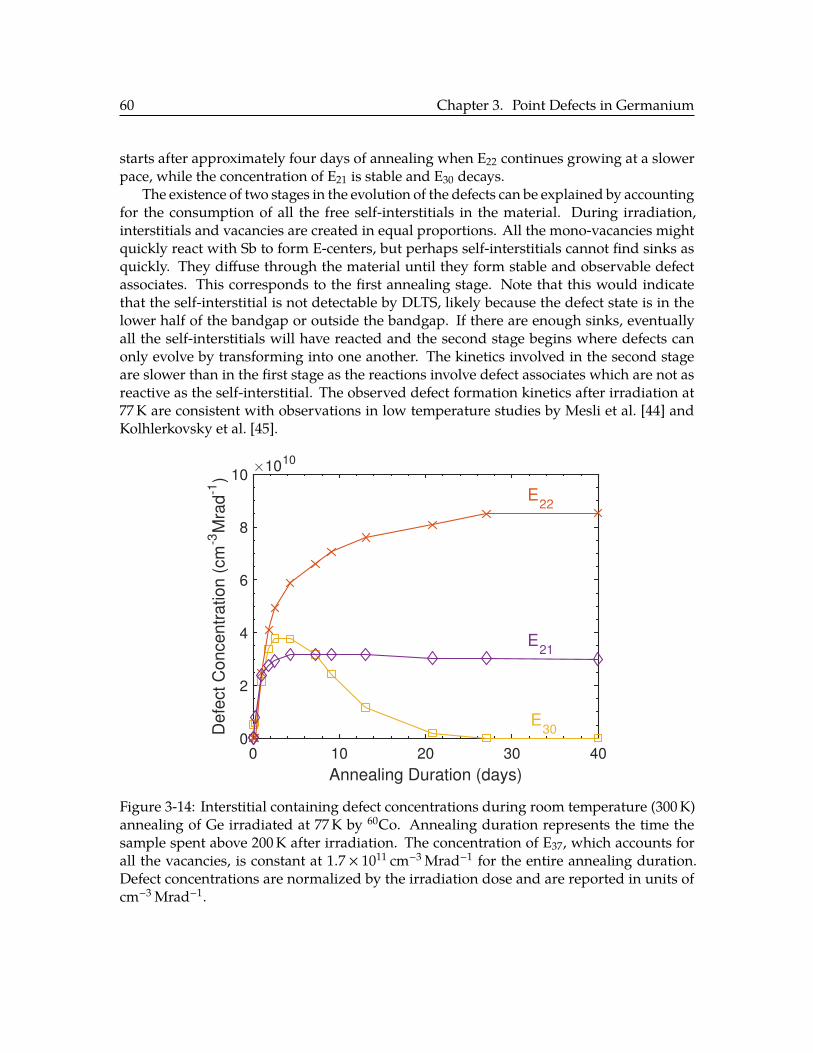
60 Chapter 3. Point Defects in Germanium
starts after approximately four days of annealing when E22 continues growing at a slower
pace, while the concentration of E21 is stable and E30 decays.
The existence of two stages in the evolution of the defects can be explained by accounting
for the consumption of all the free self-interstitials in the material. During irradiation,
interstitials and vacancies are created in equal proportions. All the mono-vacancies might
quickly react with Sb to form E-centers, but perhaps self-interstitials cannot find sinks as
quickly. They diffuse through the material until they form stable and observable defect
associates. This corresponds to the first annealing stage. Note that this would indicate
that the self-interstitial is not detectable by DLTS, likely because the defect state is in the
lower half of the bandgap or outside the bandgap. If there are enough sinks, eventually
all the self-interstitials will have reacted and the second stage begins where defects can
only evolve by transforming into one another. The kinetics involved in the second stage
are slower than in the first stage as the reactions involve defect associates which are not as
reactive as the self-interstitial. The observed defect formation kinetics after irradiation at
77 K are consistent with observations in low temperature studies by Mesli et al. [44] and
Kolhlerkovsky et al. [45].
Annealing Duration (days)
0 10 20 30 40
Defe
ct C
oncentr
ation (
cm
-3M
rad
-1)
×1010
0
2
4
6
8
10
E21
E30
E22
Figure 3-14: Interstitial containing defect concentrations during room temperature (300 K)
annealing of Ge irradiated at 77 K by60
Co. Annealing duration represents the time the
sample spent above 200 K after irradiation. The concentration of E37, which accounts for
all the vacancies, is constant at 1.7 × 10¹¹
cm−3
Mrad−1
for the entire annealing duration.
Defect concentrations are normalized by the irradiation dose and are reported in units of
cm−3
Mrad−1
.
3.2. Gamma Irradiation of Germanium 61
3.2.4.2 Irradiation at 300 K
Irradiation at room temperature was followed by anneals at higher temperatures to provide
additional information about the growth and decay of the defects. Defect concentrations
after a series of 15 minute isochronal anneals at various temperatures are plotted in Figure 3-
15. E37, E22, and E21 are all stable at room temperature. However, at room temperature, E30
will slowly decay over weeks, as was observed during room temperature annealing after
irradiation in liquid nitrogen, and is already completely removed by annealing at 85C
for 15 minutes. E37 is stable to ∼100C and is only completely removed in 15 minutes at
∼200C. At temperatures ∼100
C, E22 decays while E21 concomitantly grows. E21 is stable
to ∼150C.
Anneal Temperature (°C)
50 100 150 200
De
fect
Co
nce
ntr
atio
n (
cm
-3M
rad
-1)
×1011
0
0.5
1
1.5
2
2.5
E37
E22
E30
E21
Figure 3-15: Defect concentrations after 15 minute isochronal anneals of60
Co irradiated
Sb-doped germanium. Defect concentrations are normalized by the irradiation dose and
are reported in units of cm−3
Mrad−1
.
Isothermal anneals at multiple temperatures were used to extract annealing rates for
each defect vs. temperature. Figure 3-16 shows defect concentrations vs. annealing
durations for an isothermal anneal at 93C. All annealing reactions followed exponential
trends indicating first-order reactions. Figure 3-17 shows a plot of the annealing rate vs.
inverse temperature used to extract the frequency prefactors and activation energies of the
annealing defect reactions. A summary of the extracted parameters are shown in Table 3.2.
Spatial defect profiles were obtained before and after annealing reactions and showed that
concentrations for all defects remained homogenously distributed throughout the material
after annealing.
The isochronal and isothermal annealing data suggests a relationship between E21 and
E22. After 15 minutes at 100C (Figure 3-15), E30 has annealed out and E37 is stable, but

62 Chapter 3. Point Defects in Germanium
Annealing Duration (hours)
0 2 4 6 8 10
Defe
ct C
oncentr
ation (
cm
-3M
rad
-1)
×1011
0
0.5
1
1.5
2
2.5
E37
E21
E22
Figure 3-16: Defect concentration as a function of annealing duration at 93C. When
E22 has annealed out, E21 stops evolving whereas the decay rate of E37 is not affected.
Defect concentrations are normalized by the irradiation dose and are reported in units of
cm−3
Mrad−1
.
1000/T (K-1)
2 2.2 2.4 2.6 2.8
Annealin
g R
ate
(s
-1)
10-6
10-5
10-4
10-3
10-2
↑ E21
↓ E37
↓ E21
↓ E22
Figure 3-17: Annealing rate vs. temperature data extracted from isothermal anneals of60
Co
irradiated Sb-doped germanium. Up (↑) and down (↓) arrows next to defect labels indicate
whether the defect concentration increases or decreases upon annealing.
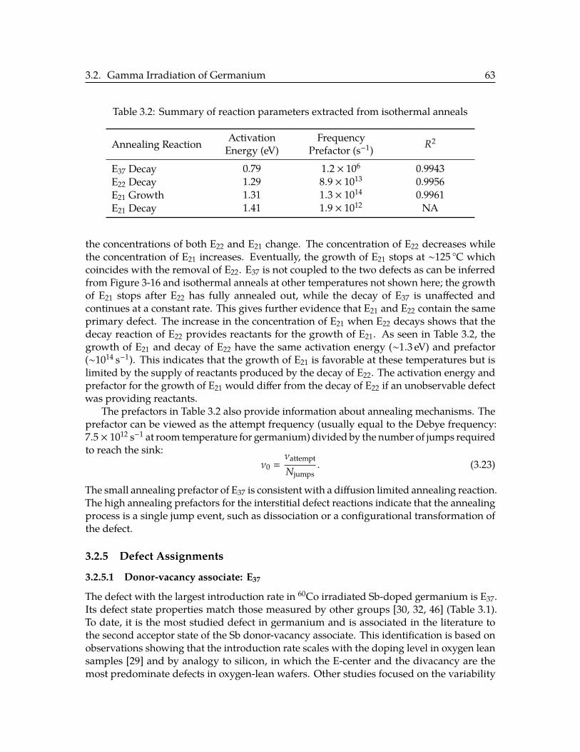
3.2. Gamma Irradiation of Germanium 63
Table 3.2: Summary of reaction parameters extracted from isothermal anneals
Annealing Reaction
Activation
Energy (eV)
Frequency
Prefactor (s−1
)
R2
E37 Decay 0.79 1.2 × 10⁶
0.9943
E22 Decay 1.29 8.9 × 10¹³
0.9956
E21 Growth 1.31 1.3 × 10¹⁴
0.9961
E21 Decay 1.41 1.9 × 10¹²
NA
the concentrations of both E22 and E21 change. The concentration of E22 decreases while
the concentration of E21 increases. Eventually, the growth of E21 stops at ∼125C which
coincides with the removal of E22. E37 is not coupled to the two defects as can be inferred
from Figure 3-16 and isothermal anneals at other temperatures not shown here; the growth
of E21 stops after E22 has fully annealed out, while the decay of E37 is unaffected and
continues at a constant rate. This gives further evidence that E21 and E22 contain the same
primary defect. The increase in the concentration of E21 when E22 decays shows that the
decay reaction of E22 provides reactants for the growth of E21. As seen in Table 3.2, the
growth of E21 and decay of E22 have the same activation energy (∼1.3 eV) and prefactor
(∼1014
s−1
). This indicates that the growth of E21 is favorable at these temperatures but is
limited by the supply of reactants produced by the decay of E22. The activation energy and
prefactor for the growth of E21 would differ from the decay of E22 if an unobservable defect
was providing reactants.
The prefactors in Table 3.2 also provide information about annealing mechanisms. The
prefactor can be viewed as the attempt frequency (usually equal to the Debye frequency:
7.5 × 10¹²
s−1
at room temperature for germanium) divided by the number of jumps required
to reach the sink:
ν0 νattempt
Njumps
. (3.23)
The small annealing prefactor of E37 is consistent with a diffusion limited annealing reaction.
The high annealing prefactors for the interstitial defect reactions indicate that the annealing
process is a single jump event, such as dissociation or a configurational transformation of
the defect.
3.2.5 Defect Assignments
3.2.5.1 Donor-vacancy associate: E37
The defect with the largest introduction rate in60
Co irradiated Sb-doped germanium is E37.
Its defect state properties match those measured by other groups [30, 32, 46] (Table 3.1).
To date, it is the most studied defect in germanium and is associated in the literature to
the second acceptor state of the Sb donor-vacancy associate. This identification is based on
observations showing that the introduction rate scales with the doping level in oxygen lean
samples [29] and by analogy to silicon, in which the E-center and the divacancy are the
most predominate defects in oxygen-lean wafers. Other studies focused on the variability
64 Chapter 3. Point Defects in Germanium
of this defect depending on the group V impurity [31] and also confirmed that this peak
is dopant related. The attribution to the second acceptor state is due to its small capture
cross section (due to coulombic repulsion between the electrons) and the absence of a
Poole Frenkel effect. However, there is no EPR confirmation of the identification of E37 as
the E-center in germanium due to the difficulties of this technique in this material. The
identification of E37 as a vacancy defect is therefore not as unambiguous as it is for the
E-center in silicon. With this reserve in mind, we will keep using the ideas that E37 is the
E-center and contains a vacancy in the following discussion, as we have until now. The
properties of E37 measured in this work are compatible with its identification as the second
acceptor state of the Sb-V pair. The high introduction rate and fast formation kinetics are a
result of the large concentration of Sb sites as sinks for mono-vacancies. The high entropy of
activation and temperature dependent cross-section indicate a bond rearrangement upon
absorption/emission of a carrier which can result from the rearrangement of the defect to
minimize the coulombic repulsion between two electrons upon transition from a singly to
doubly occupied state. As shown in Figure 3-16, the decay of E37 proceeds at a constant
rate regardless of fluctuations in the concentrations of the other defects confirming that it
contains a primary defect different from the other observed defect associates.
The smaller than Debye frequency prefactor of E37 (1.2 × 10⁶
s−1
) indicates removal of
the defect by diffusion to a sink. From Equation 3.23, the measured prefactor requires the
defect to jump ≈107
sites to reach a sink. For a 3D random walk model
〈r2
〉 3a2Njumps. (3.24)
Therefore, 107
jumps correspond to a migration distance of approximately ∼1 µm (with
nearest neighbor distance, a 0.245 nm). There are two possible sinks for E37:
1. The surface can act as a sink as was proposed by Fage-Pedersen et al. [30]. However,
diffusion to the surface would not result in first-order decay behavior nor the uniform
depth profile observed after annealing.
2. The sink can be an impurity present in the bulk of the material which is more
consistent with our observations. Based on the required migration distance of 1 µm,
the concentration of the sink would have to be ∼1012
cm−3
, which is lower than the
observed E37 concentration for doses higher than 5 Mrad. Our observation of a first
order decay reaction likely means that the sink is not saturated after removal of E37.
Therefore, each sink site can possibly accommodate multiple reactants.
The measured activation energy for the decay of E37 is not compatible with the Sb migration
activation energy measured by diffusion studies at higher temperatures [47]. Therefore,
we can assume that it is not the E-center itself that diffuses, but the mono-vacancy, after
dissociation of the E-center. Consequently, if we assume that the annealing of E37 is
diffusion limited, it implies that the annealing coefficient is proportional to the diffusivity
of the mono-vacancy times the probability of dissociation of the E-center. In this case, the
annealing activation energy is the sum of the activation energy of diffusion (migration
energy, Em) plus the activation energy of dissociation (binding energy, Eb):
Ea Em + Eb. (3.25)
3.2. Gamma Irradiation of Germanium 65
The binding energy contains a coulombic interaction as well as additional contributions.
Therefore we can estimate a lower bound for the binding energy from just the coulombic
interaction between the dissociating species from
Eb 1
4πε
q1q2
r(3.26)
where q1 and q2 are the charges of Sb and the vacancy, ε is the dielectric constant, and ris the interatomic distance (0.245 nm), which we assume separates the charges. An upper
limit on the value of the migration energy can then be roughly approximated from the
difference in our measured activation energy and our estimated binding energy. At the
temperature of annealing, the E-center is in the single acceptor state and density function
theory (DFT) calculations [48] predict the mono-vacancy to be singly negatively charged.
This yields two scenarios. If we assume that the vacancy is doubly negatively charged upon
dissociation, then we find a value of 0.75 eV for the binding energy of the E-center which
gives an experimental estimate for the migration energy of the mono-vacancy of < 0.04 eV.
If before dissociation the E-center loses an electron, then the mono-vacancy is only single
negatively charged during the dissociation, and the binding energy becomes 0.37 eV which
yields an estimate of the migration energy of < 0.4 eV.
3.2.5.2 Interstitial associates: E30, E22 and E21
E30 is a defect that has been observed before but was not thoroughly characterized. Its
measured energy level and annealing behavior are consistent with the defect E0.30 reported
by Fage-Pedersen et al. [30]. In addition, Auret et al. [46] and Roro et al. [49] also report
defects with similar states but real capture cross sections and annealing behavior were not
reported. No defects with matching properties have been reported by Nagesh et al. [29]
or Markevitch et al. [32] E21 and E22, similarly to E30 have been observed before but were
not the focus of the studies. The measured defect state and annealing behavior of E22 is
consistent with E0.23 reported by Fage-Pedersen et al. and E1 reported by Mooney et al. [28].
Its defect state also matches E0.24 reported by Auret et al. whose annealing behavior was not
reported. It was not observed by Nagesh et al. E21 matches the defect state of E0.20 reported
by Auret et al. but its annealing kinetics were not reported. E21’s defect state is close to
Fage-Pedersen et al.’s E0.19 and E0.21 but the annealing kinetics do not match perfectly. In
addition, Fage-Pedersen et al. does not observe E0.21 for all doping concentrations tested. It
is important to remember that Fage-Pedersen et al. reports more defects than other groups
in the literature and does not systematically observe them in all the wafers tested. Due to
their use of higher energy irradiation sources, different numbers of defect states would be
expected when compared to this study. E21 is not observed by Nagesh et al. or Mooney et
al.
Based on the assumption that the E-center captures all the mono-vacancies and the
observation of coupled annealing reactions, we have concluded that these three defects
contain interstitials. However none of these defects are likely the self-interstitial; they
are not present immediately after the irradiation at 77 K and their concentrations initially
grow after irradiation (Figure 3). Calculations have shown that self-interstitials can exist in
multiple configurations [50] (D, H, T, hybrid, etc.) which can each have distinct defect states
66 Chapter 3. Point Defects in Germanium
in the bandgap. Defects associates containing interstitials can also undergo a change in
configuration upon change of charge state which is why interstitial associates typically have
a large entropy of ionization, as observed for E21. Therefore, in addition to dissociation,
transitions occurring in a single jump can possibly be transformation of an associate from
one configuration into another with a different defect state. Studying the conversion these
defects states undergo during anneals at various temperatures will allow us to investigate
whether these states are different configurations of the same associate.
Transformation of E22 to E21
From the series of high temperature isothermal anneals, we showed that the decay of E21
and the growth of E22 are coupled (similar activation energy and prefactor for growth and
decay reactions as well as the saturation of E21 once E22 has annealed out). In order to
further investigate the link between these defects, their conversion ratio, (∆E21/ − ∆E22),
has been estimated as a function of the annealing temperature in Table 3.3. The data is
noisy but appears to be temperature dependent. These ratios are: (a) more than one, (b)
less than two, and (c) increase with increasing temperature. Point (a) shows that there is
possibly more than one interstitial in E22 because there cannot be a conversion ratio higher
than the ratio of primary defects per defect. Point (c) shows that there is an activation
barrier to the conversion indicating that some interstitials are lost to sinks (surface, impurity,
and/or vacancies from dissociation of E37) upon annealing at lower temperatures. Point (b)
suggests a saturation of the ratio at two which means that the conversion rate likely cannot
be higher than two. It is therefore possible that E22 contains two interstitials and E21 only
one. However, E22 containing two interstitials does not mean that E22 is the di-interstitial
because this reasoning does not rule out the possibility that it is a di-interstitial impurity
associate.
The conversion of E22 into E21 is characterized by a large prefactor, higher than the
Debye frequency which is a sign that the limiting step of the transformation consists of a
single jump. The larger than the Debye frequency magnitude can be caused by an entropic
effect; if the defect transformation results in an increase in entropy, the measured prefactor
contains an exp (∆S/k) term. A value of ∼2.5k can explain the discrepancy between the
annealing prefactor and the Debye frequency. This is consistent with the interpretation
that E22 contains two interstitials, which implies a large change of configurational and
vibrational entropy upon transformation into two E21.
Further evidence that E22 contains two interstitials is presented in Figure 3-18 which
shows the number of countable interstitials after room temperature annealing for the sample
irradiation in liquid nitrogen, assuming that the E30 and E21 contain one interstitial and E22
contains two interstitials. During the second annealing stage, the total countable interstitial
concentration does not vary as expected; if all interstitials are paired with defects, then
changes in defect concentrations only occur due to transformations from one defect into
another. In addition, the assignment that E22 contains multiple interstitials is consistent with
its small entropy of ionization compared to E21’s. We might expect that a defect containing
multiple interstitials is more configurationally constrained compared to an associate which
contains a single interstitial resulting in a smaller entropy of ionization for the multiple
interstitial containing defect.
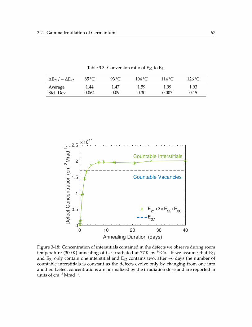
3.2. Gamma Irradiation of Germanium 67
Table 3.3: Conversion ratio of E22 to E21
∆E21/ − ∆E2285C 93
C 104
C 114
C 126
C
Average 1.44 1.47 1.59 1.99 1.93
Std. Dev. 0.064 0.09 0.30 0.007 0.15
Annealing Duration (days)
0 10 20 30 40
Defe
ct C
oncentr
ation (
cm
-3M
rad
-1)
×1011
0
0.5
1
1.5
2
2.5
E21
+2×E22
+E30
E37
Countable Vacancies
Countable Interstitials
Figure 3-18: Concentration of interstitials contained in the defects we observe during room
temperature (300 K) annealing of Ge irradiated at 77 K by60
Co. If we assume that E21
and E30 only contain one interstitial and E22 contains two, after ∼6 days the number of
countable interstitials is constant as the defects evolve only by changing from one into
another. Defect concentrations are normalized by the irradiation dose and are reported in
units of cm−3
Mrad−1
.
68 Chapter 3. Point Defects in Germanium
Transformation of E30 to E22
During the second annealing phase (Figure 3-14), E30 anneals out and fuels the growth
of E22 but does not affect the concentration of E21. If E30 dissociates and creates free
self-interstitials, then both E22 and E21 should grow during the second annealing stage as
occurs during the first stage. We propose two possible models to elucidate this problem: (a)
dissociation then fusion: E30 releases its interstitials, they diffuse and, because of a higher
activation barrier for the interstitial to form E21 rather than E22, they associate with each
other forming E22; (b) diffusion then fusion: E30 transforms into E22 without dissociating.
However, scenario (a) seems unlikely because E21 forms during the first stage of the growth
when self-interstitials are available. Scenario (b) explains why E21 stops growing during
the second phase of the annealing, but it also raises some questions. If E30 contains only
one interstitial, then, assuming that E22 contains two interstitials, the transformation either
requires one E30 to capture an interstitial or two E30 to fuse. The capture of interstitials by E30
is unlikely for the same reason that scenario (a) is unlikely; if self-interstitials are available
for reaction, the concentration of E21 should also increase. The fusion of two E30 requires
that the decay of E30 and the growth of E22 follow a second order reaction kinetics with the
same reaction rate. Currently, there is not enough data to accurately determine the reaction
orders for these defect reactions. However, the fact that E22 is initially absent during the
first 10 hours of room temperature annealing following the liquid nitrogen irradiation but
then outgrows both E21 and E30 indicates that the formation of E22 does not only involve
self-interstitials. Therefore the presence of E30 might be necessary to the formation of E22.
This adds to the likelihood of requiring the fusion of two E30 in order to form E22.
3.2.6 Formation of Secondary Defect Associates
Secondary formation of divacancies is rare in irradiated CZ silicon. The large concentration
of background impurities including oxygen at approximately 1018
cm−3
makes it unlikely
that isolated primary defects in dilute concentrations will ever react with each other before
finding an impurity with which it can associate. The environment in CZ germanium is
unique due to its much lower concentration of background impurities. Germanium is grown
in graphite crucibles instead of silica leading to low oxygen concentrations. Additionally, the
solubility of carbon in germanium is low [51] leading to low carbon impurity concentrations.
In CZ germanium, we expect the group V dopant to be the only impurity present in large
concentrations. Therefore the probability that primary defects have time to diffuse to each
other and react before finding an impurity sink is much higher in germanium than in silicon.
However, in n-type germanium, vacancies are likely negatively charged [52, 53] meaning
the formation of divacancies as secondary defects is prevented by coulombic repulsion.
Consequently divacancies are not expected to form in n-doped germanium irradiated by
60Co, neither as a primary nor secondary defect.
However, it is still worth assessing the feasibility of other species reacting in dilute con-
centrations. For diffusion-limited reactions in the case of uniform initial concentrations [54],
the solution for the concentration of the second order reaction of X + X→ P is given by
1
X
1
X0
+ κ
[1 +
2r0
(2πDt)1/2
]t (3.27)
3.3. Neutron and Alpha Irradiation of Germanium 69
where
κ 4πr02D (3.28)
and D is the diffusivity of X. Assuming r0 0.5 nm (separation distance between reactants
needed for bonding), the diffusivity, D, required for the concentration to change from
2 × 10¹⁰
cm−3
to 1 × 10¹⁰
cm−3
in one day, which corresponds to the changes observed for
E30 during the second stage of room temperature annealing of samples irradiated at 77 K
(Figure 3-14), is 4.6 × 10⁻¹⁰
cm2
s−1
.
The activation energy for diffusion can be approximated from
D 4a2νD
6
exp
(−
Ea
kT
)(3.29)
where a is the spacing between sites and νD is the Debye frequency (assuming there are four
neighboring sites). Substituting in the previously calculated value for D results in a value
of 0.4 eV for Ea. This value is not unphysical and second order defect associate formation is
not ruled out by kinetic considerations.
3.2.7 Summary
The defects generated by60
Co in 1015
cm−3
Sb-doped germanium were characterized using
DLTS to determine their electronic properties. The observed defect assignments and
annealing reactions are summarized in Figure 3-19. We observed four defects states which
exhibit two distinct behaviors, which we attributed to their nature as either an interstitial
containing or a vacancy containing defect. E37, an Sb donor-vacancy associate, decays by
dissociation and vacancy diffusion to a sink present in a concentration of 1012
cm−3
. E30,
E22, and E21 account for the interstitials created after irradiation based on the observed
formation kinetics and coupled annealing behavior. The conversion ratios of E30 into E22
and E22 into E21 suggest that E22 contains two interstitials. The formation behavior of E22
after irradiation in liquid nitrogen indicates that E30 is required for formation of E22. Neither
the mono-vacancy nor the self-interstitial could be directly observed, but their introduction
rate due to60
Co irradiation was found to be ∼2 × 10¹¹
cm−3
Mrad−1
.
3.3 Neutron and Alpha Irradiation of Germanium
In the previous section, gamma irradiation by60
Co was used to create homogeneously
distributed single displacement events. An understanding of the defects formed by reactions
of isolated vacancies and interstitials was developed which can be the basis upon which
more complicated defect associates and reactions can be interpreted. In this section, we use
alpha and neutron irradiation to generate multiple displacement events in Ge. Similar to the
last section, DLTS will be used to characterize the defects observed. Dose dependences and
annealing reactions can provide addition insights into the chemical nature of the defects.
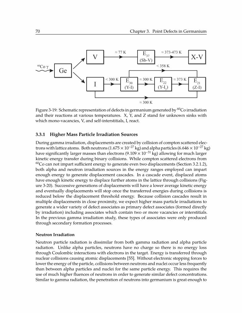
70 Chapter 3. Point Defects in Germanium
Figure 3-19: Schematic representation of defects in germanium generated by60
Co irradiation
and their reactions at various temperatures. X, Y, and Z stand for unknown sinks with
which mono-vacancies, V, and self-interstitials, I, react.
3.3.1 Higher Mass Particle Irradiation Sources
During gamma irradiation, displacements are created by collision of compton scattered elec-
trons with lattice atoms. Both neutrons (1.675 × 10⁻²⁷
kg) and alpha particles (6.646 × 10⁻²⁷
kg)
have significantly larger masses than electrons (9.109 × 10⁻³¹
kg) allowing for much larger
kinetic energy transfer during binary collisions. While compton scattered electrons from
60Co can not impart sufficient energy to generate even two displacements (Section 3.2.1.2),
both alpha and neutron irradiation sources in the energy ranges employed can impart
enough energy to generate displacement cascades. In a cascade event, displaced atoms
have enough kinetic energy to displace further atoms in the lattice through collisions (Fig-
ure 3-20). Successive generations of displacements will have a lower average kinetic energy
and eventually displacements will stop once the transferred energies during collisions is
reduced below the displacement threshold energy. Because collision cascades result in
multiple displacements in close proximity, we expect higher mass particle irradiations to
generate a wider variety of defect associates as primary defect associates (formed directly
by irradiation) including associates which contain two or more vacancies or interstitials.
In the previous gamma irradiation study, these types of associates were only produced
through secondary formation processes.
Neutron Irradiation
Neutron particle radiation is dissimilar from both gamma radiation and alpha particle
radiation. Unlike alpha particles, neutrons have no charge so there is no energy loss
through Coulombic interactions with electrons in the target. Energy is transferred through
nuclear collisions causing atomic displacements [55]. Without electronic stopping forces to
lower the energy of the particle, collisions between neutrons and nuclei occur less frequently
than between alpha particles and nuclei for the same particle energy. This requires the
use of much higher fluences of neutrons in order to generate similar defect concentrations.
Similar to gamma radiation, the penetration of neutrons into germanium is great enough to

3.3. Neutron and Alpha Irradiation of Germanium 71
IncidentParticle
Figure 3-20: Schematic of a collision cascade event with differing colors representing
successive generations (primary, secondary, and tertiary) of recoil atoms.
assume that collisions between neutrons and nuclei are homogenously distributed within
the material (based on the thickness of Ge samples). However, neutrons are able to transfer
a large amount of energy to the individual displaced atoms making collision cascades likely.
Alpha Irradiation
Unlike gamma rays and neutron radiation, alpha particles (He2+
) are charged causing a
quicker loss of energy as they pass through matter; energy is slowly lost through inelastic
scattering with electrons in the medium. As the incident particle slows down, the probability
of elastically colliding with nuclei in the material increases and eventually becomes the
primary energy loss mechanism. These collisions will create displacements if the energy
transferred is greater than the displacement threshold energy. Often, the transferred energy
is large enough that the recoiled atom can undergo further collisions with atoms thus
displacing multiple atoms per incident alpha particle. Because the majority of displacements
are generated by nuclear collisions some distance into the material (after sufficient energy
has been lost to electronic interactions), alpha irradiation results in a non-homogeneous
defect distribution. Defect distributions can be simulated using SRIM1 to calculate the
distribution of displacement events [56]. Figure 3-21 shows a SRIM simulation for the
defect distribution generated by the irradiation energy used in this work (6 MeV). SRIM
does not account for any self annihilation of Frenkel pairs and is therefore not suitable for
1Available at www.SRIM.org
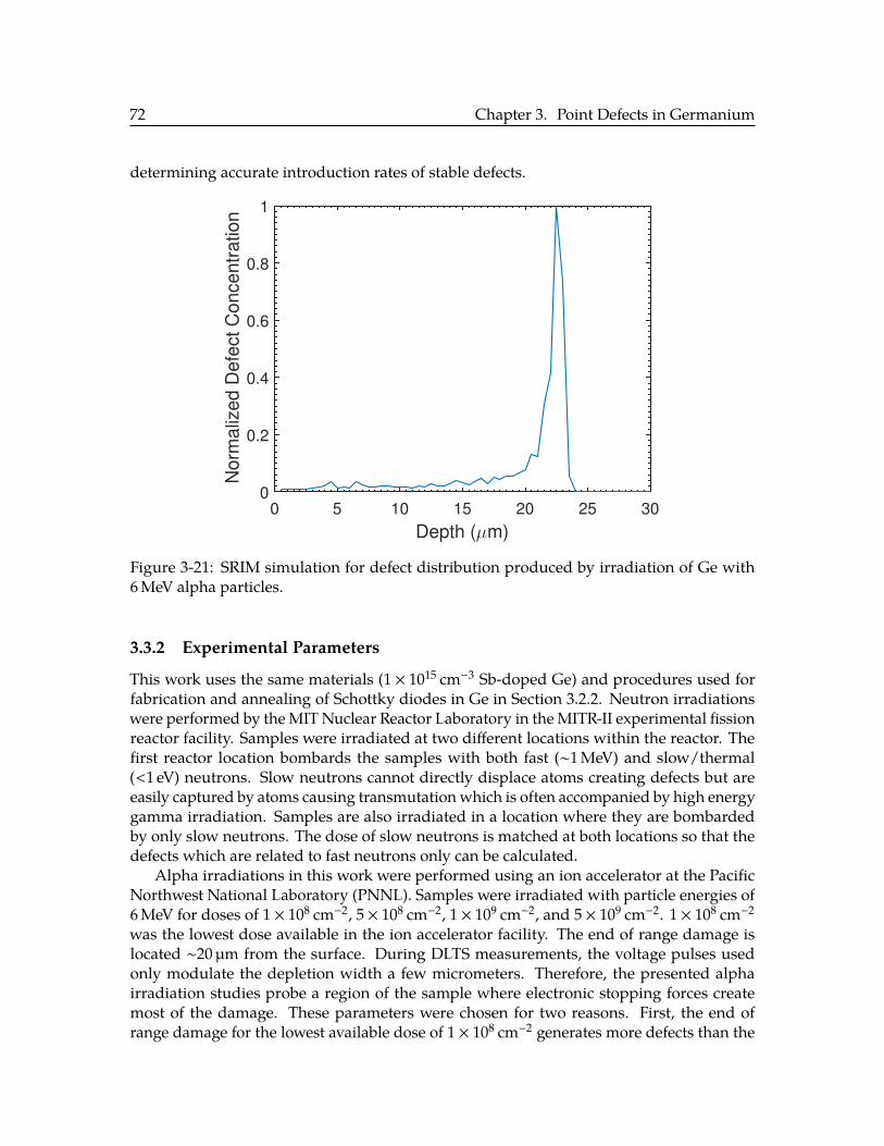
72 Chapter 3. Point Defects in Germanium
determining accurate introduction rates of stable defects.
0 5 10 15 20 25 30
Depth (µm)
0
0.2
0.4
0.6
0.8
1
No
rma
lize
d D
efe
ct
Co
nce
ntr
atio
n
Figure 3-21: SRIM simulation for defect distribution produced by irradiation of Ge with
6 MeV alpha particles.
3.3.2 Experimental Parameters
This work uses the same materials (1 × 10¹⁵
cm−3
Sb-doped Ge) and procedures used for
fabrication and annealing of Schottky diodes in Ge in Section 3.2.2. Neutron irradiations
were performed by the MIT Nuclear Reactor Laboratory in the MITR-II experimental fission
reactor facility. Samples were irradiated at two different locations within the reactor. The
first reactor location bombards the samples with both fast (∼1 MeV) and slow/thermal
(<1 eV) neutrons. Slow neutrons cannot directly displace atoms creating defects but are
easily captured by atoms causing transmutation which is often accompanied by high energy
gamma irradiation. Samples are also irradiated in a location where they are bombarded
by only slow neutrons. The dose of slow neutrons is matched at both locations so that the
defects which are related to fast neutrons only can be calculated.
Alpha irradiations in this work were performed using an ion accelerator at the Pacific
Northwest National Laboratory (PNNL). Samples were irradiated with particle energies of
6 MeV for doses of 1 × 10⁸
cm−2
, 5 × 10⁸
cm−2
, 1 × 10⁹
cm−2
, and 5 × 10⁹
cm−2
. 1 × 10⁸
cm−2
was the lowest dose available in the ion accelerator facility. The end of range damage is
located ∼20 µm from the surface. During DLTS measurements, the voltage pulses used
only modulate the depletion width a few micrometers. Therefore, the presented alpha
irradiation studies probe a region of the sample where electronic stopping forces create
most of the damage. These parameters were chosen for two reasons. First, the end of
range damage for the lowest available dose of 1 × 10⁸
cm−2
generates more defects than the

3.3. Neutron and Alpha Irradiation of Germanium 73
dopant concentration leading to compensation and inaccuracy of DLTS measurements (no
longer operating in the small signal regime). Secondly, while collision cascades are more
prevalent at the end of range, they still occur within the probed region. Therefore, we can
investigate the difference between defects (and their concentrations) generated by neutron
irradiation in which collision cascades are more dominant and electronic stopping range
alpha irradiation.
3.3.3 Defect States
DLTS spectra for 1 × 10¹⁵
cm−3
Sb-doped germanium irradiated with fast + slow neutrons
and only slow neutrons at room temperature (300 K) are shown in Figure 3-22. A third line
is plotted from the difference of the two irradiations to show the portion of the fast + slow
neutron spectra resulting from only fast neutron damage. The fast neutron fluence was
1013
cm−2
which is the lower limit of doses with which the irradiation facility can accurately
bombard samples. The slow neutron only spectrum is very similar to those generated by
60Co gamma irradiation and the electronic signatures of the defects match indicating that
the same defects are generated by both radiation types. The spectrum for damage created
by fast neutrons also contains the defects seen after60
Co gamma irradiation, however,
new peaks appear indicating the generation of new defect states. Because fast neutron
damage is expected to generate collision cascades, it is likely that the new defect states are
related to the presence of multiple vacancies or multiple interstitials. The new features
observed in the fast neutron spectrum are relatively broad making visual identification of
individual defect states by conventional DLTS difficult. One way to improve the ability
to visually distinguish overlapping defects in a DLTS conventional spectra is to compare
spectra with different filling pulses (varying capture cross sections will show varying rates
of signal saturation). Because Laplace DLTS gives the highest resolution, we have used
that to identify 11 distinct defect states whose locations are roughly signified on a plot of
conventional spectra taken with varying pulse widths (Figure 3-23). Of the 11 observed
defect states, 3 were previously generated by gamma irradiations (E37, E22, and E21). The
newly observed defects are also named based on their apparent enthalpies but have been
given a prefix of N to signify that they were observed after neutron irradiation. Figure 3-24
shows emission rate vs. temperature data for defect states observed after neutron irradiation.
This data was analyzed to extract apparent activation enthalpies and apparent capture cross
sections. Pulse-filling measurements were performed at various temperatures to measure
real capture cross sections and determine temperature dependencies if present for 5 of the
newly observed defects. Accurate capture cross section measurements for 3 of the defects
were not possible due to difficulty of deconvolution of defect states even with Laplace
DLTS. A summary of properties extracted from DLTS measurements for the observed
defect states after neutron irradiation at 300 K is listed in Table 3.4. Measurements of alpha
irradiated samples show the generation of the same defects as after neutron irradiation
but in lower concentrations relative to the defects generated by single displacements after
gamma irradiation. This is consistent with our expectation that the depth of the material
probed in alpha irradiated samples have less collision cascades than the bulk of the neutron
irradiated material.
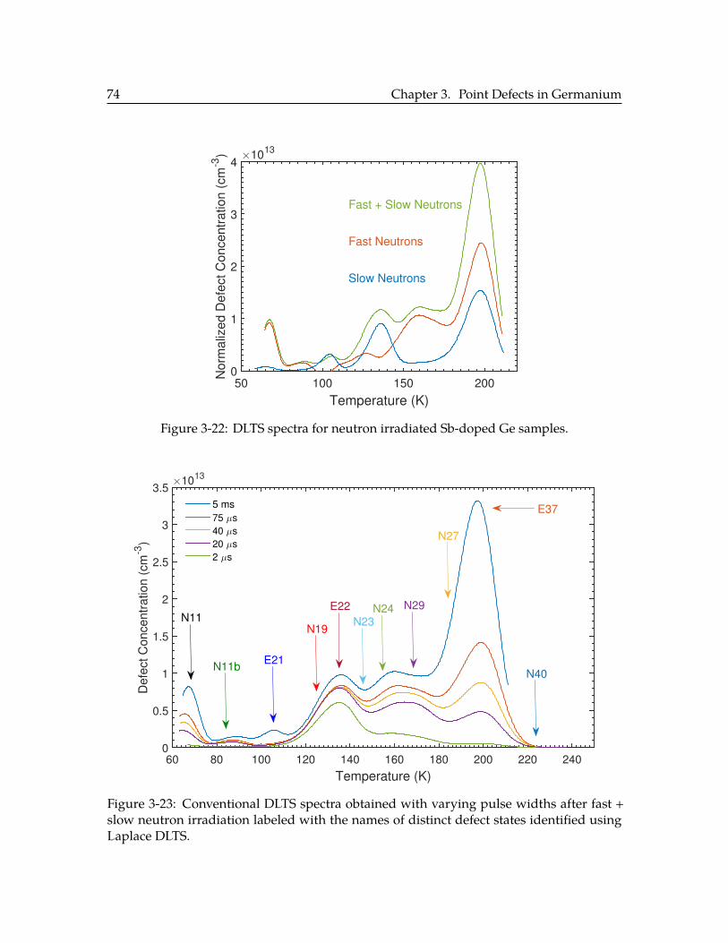
74 Chapter 3. Point Defects in Germanium
Temperature (K)
50 100 150 200
Norm
aliz
ed D
efe
ct
Con
centr
ation (
cm
-3) ×10
13
0
1
2
3
4
Fast + Slow Neutrons
Fast Neutrons
Slow Neutrons
Figure 3-22: DLTS spectra for neutron irradiated Sb-doped Ge samples.
Temperature (K)
60 80 100 120 140 160 180 200 220 240
Defe
ct C
oncentr
ation (
cm
-3)
×1013
0
0.5
1
1.5
2
2.5
3
3.5
5 ms
75 µs
40 µs
20 µs
2 µs
N27
N40
E37
N29N24N23
E22
N19
E21
N11
N11b
Figure 3-23: Conventional DLTS spectra obtained with varying pulse widths after fast +
slow neutron irradiation labeled with the names of distinct defect states identified using
Laplace DLTS.
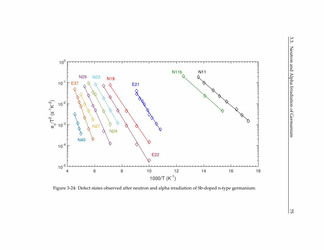
3.3.
Neu
tron
an
dA
lp
ha
Irrad
iation
of
Germ
an
iu
m75
1000/T (K-1
)
4 6 8 10 12 14 16 18
en/T
2 (
s-1
K-2
)
10-5
10-4
10-3
10-2
10-1
100
N27
E37
N29
N24
N23
E22
N19
E21
N11b N11
N40
Figure 3-24: Defect states observed after neutron and alpha irradiation of Sb-doped n-type germanium.
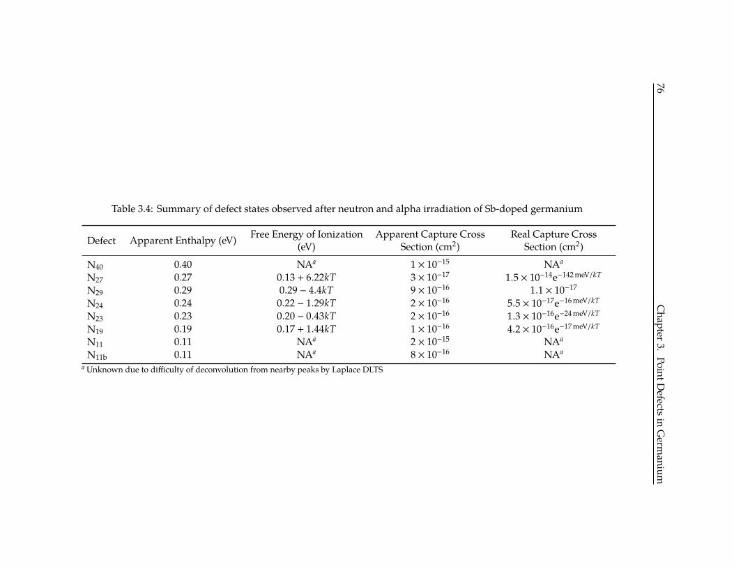
76
Ch
ap
ter
3.
Poin
tD
efects
in
Germ
an
iu
m
Table 3.4: Summary of defect states observed after neutron and alpha irradiation of Sb-doped germanium
Defect Apparent Enthalpy (eV)
Free Energy of Ionization
(eV)
Apparent Capture Cross
Section (cm2)
Real Capture Cross
Section (cm2)
N400.40 NA
a1 × 10
−15NA
a
N270.27 0.13 + 6.22kT 3 × 10
−171.5 × 10
−14e−142 meV/kT
N290.29 0.29 − 4.4kT 9 × 10
−161.1 × 10
−17
N240.24 0.22 − 1.29kT 2 × 10
−165.5 × 10
−17e−16 meV/kT
N230.23 0.20 − 0.43kT 2 × 10
−161.3 × 10
−16e−24 meV/kT
N190.19 0.17 + 1.44kT 1 × 10
−164.2 × 10
−16e−17 meV/kT
N110.11 NA
a2 × 10
−15NA
a
N11b0.11 NA
a8 × 10
−16NA
a
aUnknown due to difficulty of deconvolution from nearby peaks by Laplace DLTS
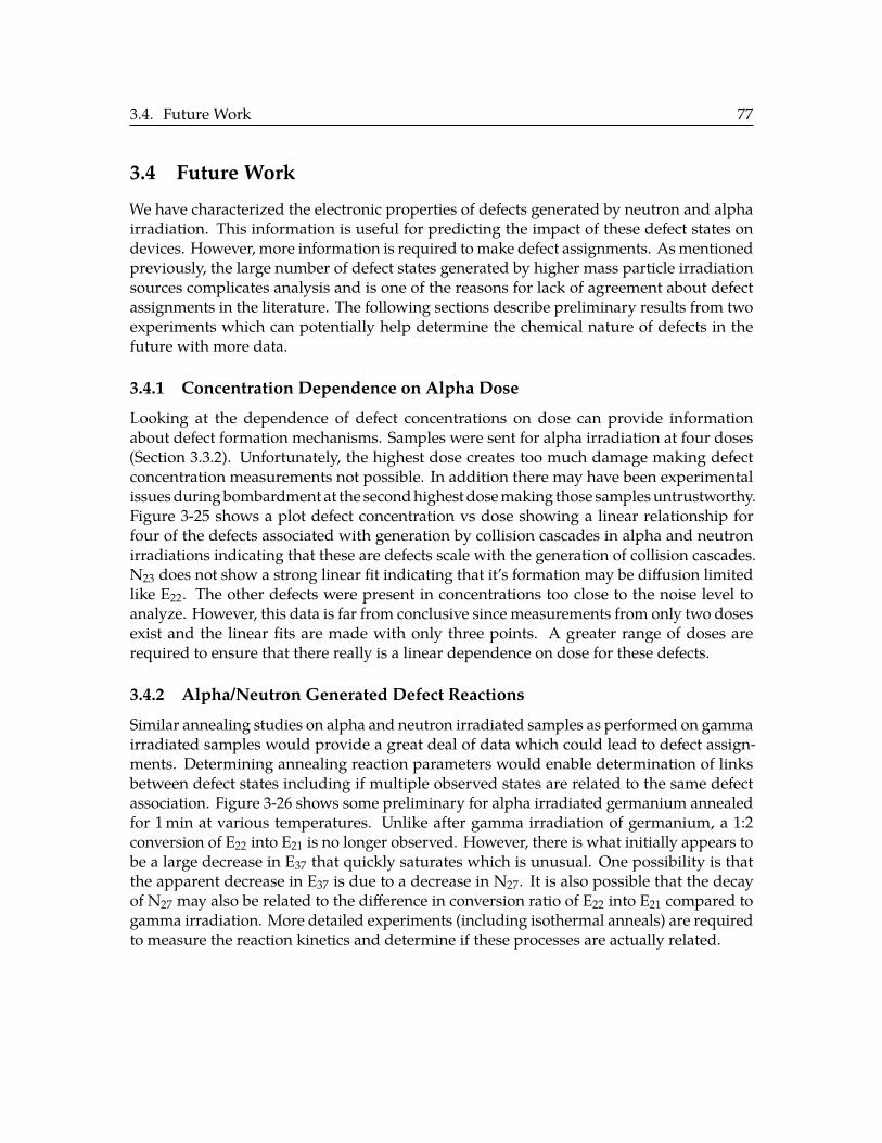
3.4. Future Work 77
3.4 Future WorkWe have characterized the electronic properties of defects generated by neutron and alpha
irradiation. This information is useful for predicting the impact of these defect states on
devices. However, more information is required to make defect assignments. As mentioned
previously, the large number of defect states generated by higher mass particle irradiation
sources complicates analysis and is one of the reasons for lack of agreement about defect
assignments in the literature. The following sections describe preliminary results from two
experiments which can potentially help determine the chemical nature of defects in the
future with more data.
3.4.1 Concentration Dependence on Alpha Dose
Looking at the dependence of defect concentrations on dose can provide information
about defect formation mechanisms. Samples were sent for alpha irradiation at four doses
(Section 3.3.2). Unfortunately, the highest dose creates too much damage making defect
concentration measurements not possible. In addition there may have been experimental
issues during bombardment at the second highest dose making those samples untrustworthy.
Figure 3-25 shows a plot defect concentration vs dose showing a linear relationship for
four of the defects associated with generation by collision cascades in alpha and neutron
irradiations indicating that these are defects scale with the generation of collision cascades.
N23 does not show a strong linear fit indicating that it’s formation may be diffusion limited
like E22. The other defects were present in concentrations too close to the noise level to
analyze. However, this data is far from conclusive since measurements from only two doses
exist and the linear fits are made with only three points. A greater range of doses are
required to ensure that there really is a linear dependence on dose for these defects.
3.4.2 Alpha/Neutron Generated Defect Reactions
Similar annealing studies on alpha and neutron irradiated samples as performed on gamma
irradiated samples would provide a great deal of data which could lead to defect assign-
ments. Determining annealing reaction parameters would enable determination of links
between defect states including if multiple observed states are related to the same defect
association. Figure 3-26 shows some preliminary for alpha irradiated germanium annealed
for 1 min at various temperatures. Unlike after gamma irradiation of germanium, a 1:2
conversion of E22 into E21 is no longer observed. However, there is what initially appears to
be a large decrease in E37 that quickly saturates which is unusual. One possibility is that
the apparent decrease in E37 is due to a decrease in N27. It is also possible that the decay
of N27 may also be related to the difference in conversion ratio of E22 into E21 compared to
gamma irradiation. More detailed experiments (including isothermal anneals) are required
to measure the reaction kinetics and determine if these processes are actually related.
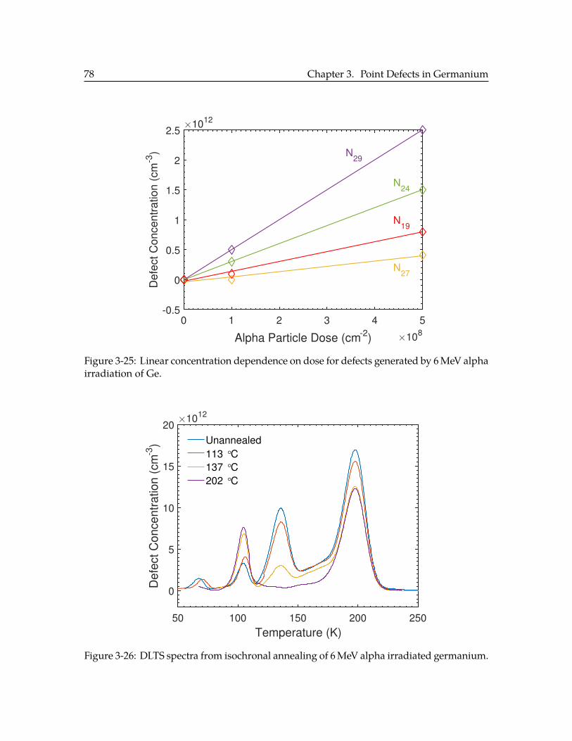
78 Chapter 3. Point Defects in Germanium
0 1 2 3 4 5
Alpha Particle Dose (cm-2
) ×108
-0.5
0
0.5
1
1.5
2
2.5
De
fect
Co
nce
ntr
atio
n (
cm
-3)
×1012
N27
N19
N24
N29
Figure 3-25: Linear concentration dependence on dose for defects generated by 6 MeV alpha
irradiation of Ge.
50 100 150 200 250
Temperature (K)
0
5
10
15
20
De
fect
Co
nce
ntr
atio
n (
cm
-3)
×1012
Unannealed
113 °C
137 °C
202 °C
Figure 3-26: DLTS spectra from isochronal annealing of 6 MeV alpha irradiated germanium.
Chapter 4
Germanium-on-Silicon Laser
A key application for an on-chip light source is in high performance computing. For decades,
the microelectronics industry has been driven to continually scale down components in order
to follow Moore’s Law [58] which states that the number of transistors on a microprocessor
chip will double approximately every two years. In the past, the shrinking of component
sizes has lead to equally impressive gains in computing performance. However, continued
scaling has become increasingly difficult. Eventually fundamental limits will be reached
requiring innovation beyond component scaling for performance improvements in the
future. 2016 is the first year that the International Technology Roadmap for Semiconductors
(ITRS) is not centered around continuation of Moore’s Law.
As seen in Figure 4-1, while the number of transistors per chip has steadily increased over
time, clock speeds saturated in the early 2000s [59] due to limitations imposed by the excess
heat generated at high clock speeds. A large factor for the increased power dissipation is the
increase in the RC delay of the electrical interconnects. When scaling components, shrinking
wire diameters increase resistance while decreasing wire pitches increase capacitance. In
order to continue increasing performance, chips are now manufactured with multiple
processors (also referred to as “cores”). However, this method also cannot scale indefinitely
as communication between distant components requires increasing bandwidth and power
consumption requirements which cannot be satisfied by electrical interconnects. One
potential solution is to switch to optical interconnects which can provide higher bandwidth
density at lower energy costs [1, 2].
Building CMOS compatible optical interconnect systems using a silicon microphotonics
platform will facilitate integration of optical interconnects with established microelectronics
architectures . Furthermore, fabrication of silicon microphotonic components can leverage
processing techniques and equipment developed by the microelectronics industry to reduce
costs [3]. A complete optical interconnect system requires all the components needed to
make electrical to optical (EO) and optical to electrical (OE) signal transformations. For
systems operating in the near-IR, silicon itself provides a satisfactory material for fabrication
of passive components such as waveguides and ring resonator filters. Single mode silicon
waveguides can be fabricated with optical losses less than 1 dB cm−1
[60]. Additionally, high
The work in this chapter is partially adapted from [57] and was done in collaboration with R. Camacho-Aguilera
and Y. Cai, also members of the Kimerling group at MIT.
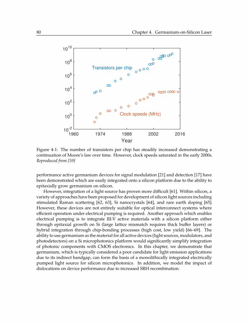
80 Chapter 4. Germanium-on-Silicon Laser
Year
1960 1974 1988 2002 201610
-2
100
102
104
106
108
1010
Transistors per chip
Clock speeds (MHz)
Figure 4-1: The number of transistors per chip has steadily increased demonstrating a
continuation of Moore’s law over time. However, clock speeds saturated in the early 2000s.
Reproduced from [59]
performance active germanium devices for signal modulation [21] and detection [17] have
been demonstrated which are easily integrated onto a silicon platform due to the ability to
epitaxially grow germanium on silicon.
However, integration of a light source has proven more difficult [61]. Within silicon, a
variety of approaches have been proposed for development of silicon light sources including
stimulated Raman scattering [62, 63], Si nanocrystals [64], and rare earth doping [65].
However, these devices are not entirely suitable for optical interconnect systems where
efficient operation under electrical pumping is required. Another approach which enables
electrical pumping is to integrate III-V active materials with a silicon platform either
through epitaxial growth on Si (large lattice mismatch requires thick buffer layers) or
hybrid integration through chip-bonding processes (high cost, low yield) [66–69]. The
ability to use germanium as the material for all active devices (light sources, modulators, and
photodetectors) on a Si microphotonics platform would significantly simplify integration
of photonic components with CMOS electronics. In this chapter, we demonstrate that
germanium, which is typically considered a poor candidate for light emission applications
due to its indirect bandgap, can form the basis of a monolithically integrated electrically
pumped light source for silicon microphotonics. In addition, we model the impact of
dislocations on device performance due to increased SRH recombination.
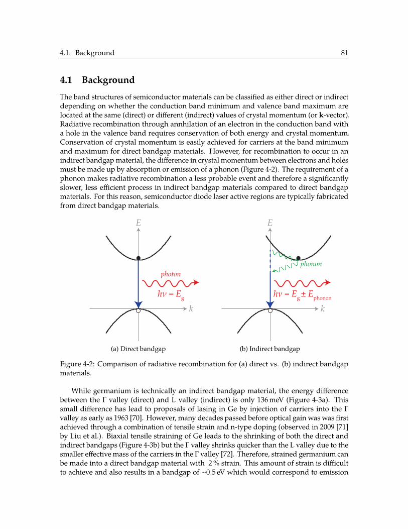
4.1. Background 81
4.1 BackgroundThe band structures of semiconductor materials can be classified as either direct or indirect
depending on whether the conduction band minimum and valence band maximum are
located at the same (direct) or different (indirect) values of crystal momentum (or k-vector).
Radiative recombination through annhilation of an electron in the conduction band with
a hole in the valence band requires conservation of both energy and crystal momentum.
Conservation of crystal momentum is easily achieved for carriers at the band minimum
and maximum for direct bandgap materials. However, for recombination to occur in an
indirect bandgap material, the difference in crystal momentum between electrons and holes
must be made up by absorption or emission of a phonon (Figure 4-2). The requirement of a
phonon makes radiative recombination a less probable event and therefore a significantly
slower, less efficient process in indirect bandgap materials compared to direct bandgap
materials. For this reason, semiconductor diode laser active regions are typically fabricated
from direct bandgap materials.
E
khν = Eg
photon
(a) Direct bandgap
phonon
hν = Eg ± Ephonon
k
E
(b) Indirect bandgap
Figure 4-2: Comparison of radiative recombination for (a) direct vs. (b) indirect bandgap
materials.
While germanium is technically an indirect bandgap material, the energy difference
between the Γ valley (direct) and L valley (indirect) is only 136 meV (Figure 4-3a). This
small difference has lead to proposals of lasing in Ge by injection of carriers into the Γ
valley as early as 1963 [70]. However, many decades passed before optical gain was was first
achieved through a combination of tensile strain and n-type doping (observed in 2009 [71]
by Liu et al.). Biaxial tensile straining of Ge leads to the shrinking of both the direct and
indirect bandgaps (Figure 4-3b) but the Γ valley shrinks quicker than the L valley due to the
smaller effective mass of the carriers in the Γ valley [72]. Therefore, strained germanium can
be made into a direct bandgap material with 2 % strain. This amount of strain is difficult
to achieve and also results in a bandgap of ∼0.5 eV which would correspond to emission

82 Chapter 4. Germanium-on-Silicon Laser
at a wavelength of ∼2500 nm. It is more desirable to have emission in a wavelength range
closer to standard communications wavelengths of ∼1550 nm where mature technologies
for modulation and detection exist. In addition, photodetectors designed for operation
at longer wavelengths would need smaller bandgaps which would significantly increase
leakage current. Instead, germanium can be slightly strained (0.2 % to 0.3 %) and highly
n-type doped to yield a pseudo-direct bandgap (Figure 4-3c). When the n-type doping
concentration is ∼1019
cm−3
, the lower energy states in the L valley become occupied. When
electrons are now injected, some electrons will occupy the Γ valley and can thus efficiently
radiatively recombine with holes in the valence band. In addition, the higher recombination
rate of electrons in the Γ valley leads to inter-valley scattering of electrons from the L valley
to the Γ valley in order to maintain quasi-equilibrium in the conduction band. This further
increases the efficiency of radiative recombination from the Γ valley. Theoretically predicted
gain spectra for 0.25 % strained mid-1 × 10¹⁹
cm−3
doped germanium show broad net gain
is possible from 1550 nm to 1600 nm. This would suggest that a germanium laser would be
suitable for on-chip wavelength division multiplexing (WDM) applications.
<111>k
L
0.80
0 eV
0.66
4 eV
<111>k
E
L
<111>k
E
L
electrons fromn-type doping
bulk Ge tensile strained intrinsic Ge tensile strained n+ Ge
photons
Light hole band
heavy hole band
Injectedelectrons
Injected holes
hv
<111>
E
Γ
(a)
<111>
(b)
<111>
(c)
Γ Γ
Conduction band
Light hole band
heavy hole bandInjected holes
Figure 4-3: Schematic band structure of (a) bulk germanium, (b) tensile strained intrinsic
Ge, and (c) tensile strained n+
Ge. Reprinted from [73] with permission
4.2 Ge Laser Fabrication and DesignThis section contains a brief overview of processes crucial to the development of a Ge laser
largely developed by collaborators, primarily R. Camacho-Aguilera [74] and Y. Cai [75] (see
the referenced theses for more details).

4.2. Ge Laser Fabrication and Design 83
4.2.1 Epitaxial Growth of Ge on Si via UHVCVD
Integral to implementation of an integrated germanium laser on silicon is the growth
of high quality germanium on silicon. Heteroepitaxy of Ge on Si can be challenging
due to the difference of lattice constants between Si (5.431 Å) and Ge (5.658 Å). The 4 %
lattice mismatch leads to islanding of Ge when the thickness reaches a critical thickness
(Stranski–Krastanov growth). One approach to fabricating uniform films is to gradually
grade the composition of a SiGe buffer layer so that the strain is never large enough to
force islanding [76]. However, this method requires thick buffer layers which can be
time consuming and costly to fabricate. In addition, for many integrated microphotonic
applications, it is desirable to be able to fabricate the germanium devices close to the silicon
(without a thick buffer) in order to couple light from passive to active components and vice
versa. Another approach, which is used in this work, is to instead use a two-step ultra-high
vacuum chemical vapor deposition (UHVCVD) growth process whereby an initial low
temperature (360C) growth is used to make a continuous and thin (40 nm to 60 nm) buffer
layer which accommodates strain in the germanium [77]. As previously mentioned, Ge will
island to relieve strain that builds up the film thickness increases. However, during a low
temperature growth, Ge is not mobile enough to island. Strain is instead released through
the nucleation of misfit dislocations (Section 2.2.2). Once the strain has been completely
relaxed, the growth temperature is increased (650C to 780
C) to grow high quality Ge
via homoepitaxy. Threading dislocation densities after growth are typically as high as
108
cm−2
to 109
cm−2
. However, annealing or cyclic annealing of films at high temperatures
can reduce threading dislocation densities down to ∼2 × 10⁷
cm−2
for 1 µm thick blanket
films or ∼1 × 10⁶
cm−2
for 10 µm × 10 µm mesas selectively grown in SiO2 trenches [77].
High temperature growth and annealing steps also play a crucial role in introducing
tensile strain to the film which is necessary for a pseudo-direct bandgap (Section 4.1). A
common misconception is that Ge will be placed into compressive strain due to its larger
lattice constant compared to Si. This would be true for very thin films which would
grow pseudomorphically. However, for practical Ge devices, in order to confine light at
∼1550 nm, film thicknesses would need to be at least a few hundred nanometers. This is
much thicker than the critical thickness for pseudomorphic growth and instead during
the high temperature anneal (or high temperature Ge growth step), the material becomes
completely strain relaxed through nucleation of misfit dislocations. However, upon cooling
to room temperature, germanium will shrink more than silicon due to a larger coefficient
of thermal expansion. This places the germanium film into a state of biaxial tensile strain
which can be calculated from
ε
∫ Ti
Tf
(αGe − αSi) dT (4.1)
where Ti and Tf are the initial and final (room) temperatures, αGe is the linear expan-
sion coefficient of Ge (5.9 × 10⁻⁶
C−1
), and αSi is the linear expansion coefficient of Si
(2.6 × 10⁻⁶
C−1
). Experimentally, annealing temperatures between 650C to 850
C will
lead to measured tensile strains of 0.2 % to 0.25 %.
UHVCVD growth of Ge occurs selectively on Si but not on SiO2 which has two significant

84 Chapter 4. Germanium-on-Silicon Laser
benefits. The first is that Ge structures can be defined in the material without first depositing
a blanket film and then etching. Dry etching of Ge can lead to rough sidewalls (optical
scattering) and dangling bonds (carrier recombination) which would contribute to poor
device performance. Instead of requiring passivation after etching, Ge grown within
trenches are already passivated by the oxide trench walls. The second benefit is that the
oxide walls provide a surface for threading dislocations to annihilate at during annealing.
Therefore, lower threading dislocation densities can be achieved for confined Ge structures
vs. blanket films.
4.2.2 Germanium n-type Doping
Net optical gain (which is a requirement for lasing) is observed when the optical gain exceeds
the losses in the system, a major loss being free carrier absorption (FCA). Previously, both
net optical gain and optically pumped lasing [78] have been demonstrated from 1019
cm−3
n-type doped, tensile-strained germanium showing that overcoming FCA is possible in
order to attain net gains of ∼50 cm−1
. However, electrically pumped laser designs contain
significant additional losses (>100 cm−1
from free carrier absorption in heavily doped
electrodes (required for efficient carrier injection). To overcome these additional losses,
increased n-type doping levels are required in order to boost the optical gain from Ge [79].
Germanium can be doped in situ with phosphorous during UHVCVD growth by
use of PH3. However, the maximum activated phosphorous concentration is limited to
∼2 × 10¹⁹
cm−3
for growth temperatures 600C to 700
C [80]. Above ∼750
C, phosphorous
out diffuses and evaporates reducing n-type doping concentrations. Greater concentrations
can be achieved during low temperature Ge growths but results in poorer quality Ge
material [81]. Ion implantation is commonly used process for introduction of dopant atoms
in microelectronics circuits. However, implantation requires bombarding the material with
high energy ions which creates significant numbers of defects which will act as non-radiative
recombination centers reducing device performance. Annealing can be used to remove
implantation damage but can also result in dopant out-diffusion ultimately limiting the
doping concentration.
In our work, we use a delta-doping approach to obtain n-type doping concentration
>4 × 10¹⁹
cm−3
while maintaining good material quaility [82]. After CVD growth of the
active layer Ge film, alternative layers of P monolayers and intrinsic Ge are grown at low
temperatures (450C and 400
C respectively) to form a delta layer stack with a large P
concentration which can act as a P source for indiffusion (Figure 4-4). The diffusivity
of P atoms varies quadratically with concentration which allows for in-diffusion during
annealing to beat out-diffusion to the Ge surface and Ge/Si interface creating uniform
doping profiles in the active Ge region [83].
4.2.3 p+Si/n+Ge/n+Si Double Heterostructure
The overall device structure must be designed in order to allow for efficient electron and
hole injection throughout the active germanium region. Most common III-V diode lasers
implement a double heterostructure design where a lower bandgap material (active device
layer) is sandwiched between a larger bandgap material [84]. This allows for confinement

4.2. Ge Laser Fabrication and Design 85
Si Substrate
Undoped Ge
n+ Ge
Phosphorus
Figure 4-4: Schematic of delta doping layers which act as a dopant reservoir for phosphorous
atoms
of both free carriers and light to the active region improving laser efficiency. Our work
also utilizes a double heterostructure design by confining carriers and photons to Ge by
sandwiching it between the n+
Si substrate on which Ge is grown and a p+
plasma enhanced
CVD (PECVD) deposited film of amorphous silicon into which boron is implanted. In
addition to the active region being composed of an indirect bandgap material, our laser
design is different from typical III-V heterostructure designs in two significant ways. First,
typical double heterostructure devices utilize a p-i-n diode whereas we employ a p-n-n
structure. This may lead to concerns that a junction only forms at the n+
Ge/p+
Si interface.
However, simulations show that the heavy doping of silicon leads to built-in voltages
at both interfaces allowing for injection of electrons and holes throughout the entire Ge
region[79]. Second, in III-V lasers, the two different semiconductors are chosen such that
the heterostructure has a Type-I band alignment where as Si/Ge interfaces typically show
Type-II band alignment. This may lead to concerns that sufficient injection of carriers
into this structure is not possible. Figure 4-5 shows a simulation of the heterostructure
bands which predicts that due to the heavy n-type doping of Ge, under forward bias,
band bending creates a pseudo Type-I alignment [73]. Furthermore, predicted carrier
concentrations shows that large hole concentrations can be achieved in the active region
despite its heavy n-type doping. Therefore, a p+
Si/n+
Ge/n+
Si double heterostructure is a
suitable design for development of an electrically pumped laser.
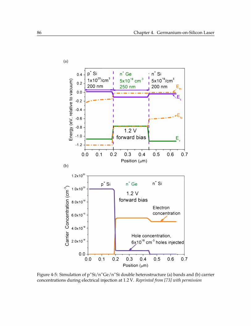
86 Chapter 4. Germanium-on-Silicon Laser
(a)
(b)
Figure 4-5: Simulation of p+
Si/n+
Ge/n+
Si double heterostructure (a) bands and (b) carrier
concentrations during electrical injection at 1.2 V. Reprinted from [73] with permission
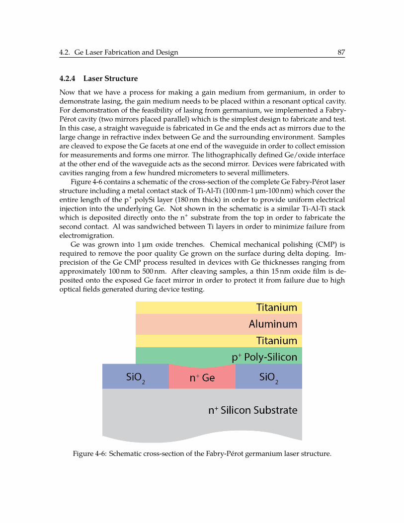
4.2. Ge Laser Fabrication and Design 87
4.2.4 Laser Structure
Now that we have a process for making a gain medium from germanium, in order to
demonstrate lasing, the gain medium needs to be placed within a resonant optical cavity.
For demonstration of the feasibility of lasing from germanium, we implemented a Fabry-
Pérot cavity (two mirrors placed parallel) which is the simplest design to fabricate and test.
In this case, a straight waveguide is fabricated in Ge and the ends act as mirrors due to the
large change in refractive index between Ge and the surrounding environment. Samples
are cleaved to expose the Ge facets at one end of the waveguide in order to collect emission
for measurements and forms one mirror. The lithographically defined Ge/oxide interface
at the other end of the waveguide acts as the second mirror. Devices were fabricated with
cavities ranging from a few hundred micrometers to several millimeters.
Figure 4-6 contains a schematic of the cross-section of the complete Ge Fabry-Pérot laser
structure including a metal contact stack of Ti-Al-Ti (100 nm-1 µm-100 nm) which cover the
entire length of the p+
polySi layer (180 nm thick) in order to provide uniform electrical
injection into the underlying Ge. Not shown in the schematic is a similar Ti-Al-Ti stack
which is deposited directly onto the n+
substrate from the top in order to fabricate the
second contact. Al was sandwiched between Ti layers in order to minimize failure from
electromigration.
Ge was grown into 1 µm oxide trenches. Chemical mechanical polishing (CMP) is
required to remove the poor quality Ge grown on the surface during delta doping. Im-
precision of the Ge CMP process resulted in devices with Ge thicknesses ranging from
approximately 100 nm to 500 nm. After cleaving samples, a thin 15 nm oxide film is de-
posited onto the exposed Ge facet mirror in order to protect it from failure due to high
optical fields generated during device testing.
Figure 4-6: Schematic cross-section of the Fabry-Pérot germanium laser structure.
88 Chapter 4. Germanium-on-Silicon Laser
4.3 Electrical Pumping of Ge Laser Diodes
4.3.1 Experimental Apparatus
Emission from the laser devices was collected and measured using a Horiba micro-
photoluminescence (PL) system equipped with a LN2 cooled InGaAs photodetector. The
micro-PL system collects light through a microscope objective and passes it through a
diffraction grating which acts as a monochromator before being collected at the detector.
Emission spectra are obtained by sequentially varying the wavelengths allowed through
the monochromator. The resolution of the obtained spectrum is determined by the step
size and slit width and has been calibrated using a narrow linewidth commercial 1550 nm
laser. In our experiments, the resolution varies from approximately 10 nm (wide slit width
for maximum signal intensity) to 1 nm.
After cleaving to form mirror facets, chips containing a row of lasers were mounted to
a metal block which is cooled by a thermoelectric cooler whose hot-side is actively cooled
using a LN2 cooling system. A thermocouple is used to measure the temperature of the
metal block as close to the sample as possible and provide feedback for the thermoelectric
cooler. The temperature was maintained at 15C for electrical pumping measurements.
Nitrogen gas was gently flown over the samples to prevent any condensation that may from
due to cooling.
Samples are oriented such that the emission is directed into the microscope objective
of the micro-PL system. The system contains a switch to allow for light collected from
the objective to be fed to a camera which aids in alignment of the Ge facets for efficient
collection. A second camera is oriented perpendicular to the microscope objective and is
used to give a top-down view of the chip for contacting to the metal pads with tungsten
probe tips using XYZ micromanipulator stages. Electrical injection is supplied by a constant
current pulsed laser driver whose pulsed signal is sent to a lock-in amplifier to be used as
a reference for improving signal/noise from the photodetector. A schematic of the laser
emission measurement setup is found in Figure 4-7.
4.3.2 Demonstration of Electrically Pumped Lasing
Initial testing of devices at large duty cycles (∼50 %) yielded ambiguous results regarding
whether lasing was occurring. At low injection current densities, no emission was detectable
but for some devices a threshold was seen where a brief but intense signal detection
was observed followed quickly by device failure. The time before failure was quick
enough that spectra and accurate determination of emission center wavelengths were
unobtainable. Some devices failed before observation of emission which was likely a result
of the monochromator never sweeping the emission wavelength before device failure.
Even though samples are cooled to 15C with a thermoelectric cooler, local heating in the
device can be much greater and possibly leading to the observed failure. To reduce heating
due to the injection current, shorter duty cycles (∼4 %) were implemented. Initially, similar
brief intense emission events were not observed even though devices were not exhibiting
failure. The current was then directly measured using an inductive sensor connected to
an oscilloscope in order to verify that the intended pulses are being generated. For the
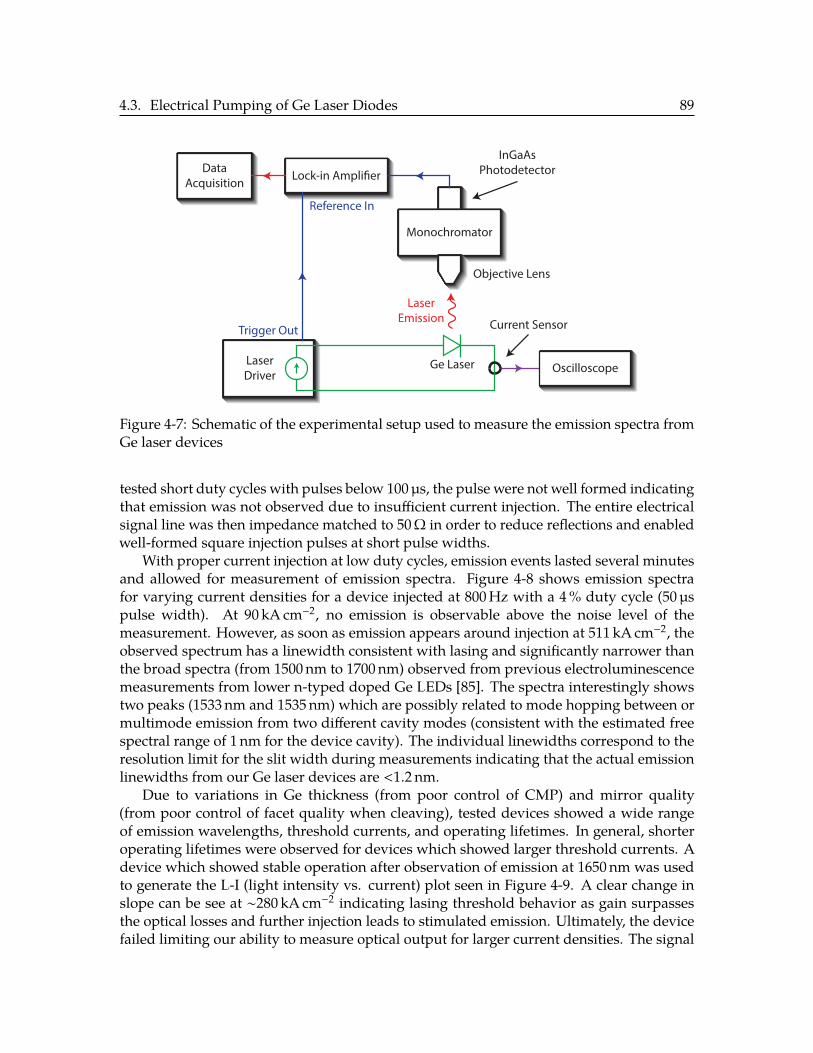
4.3. Electrical Pumping of Ge Laser Diodes 89
LaserDriver
Monochromator
Lock-in Amplier
Oscilloscope
DataAcquisition
Ge Laser
Current Sensor
LaserEmission
Objective Lens
InGaAsPhotodetector
Trigger Out
Reference In
Figure 4-7: Schematic of the experimental setup used to measure the emission spectra from
Ge laser devices
tested short duty cycles with pulses below 100 µs, the pulse were not well formed indicating
that emission was not observed due to insufficient current injection. The entire electrical
signal line was then impedance matched to 50Ω in order to reduce reflections and enabled
well-formed square injection pulses at short pulse widths.
With proper current injection at low duty cycles, emission events lasted several minutes
and allowed for measurement of emission spectra. Figure 4-8 shows emission spectra
for varying current densities for a device injected at 800 Hz with a 4 % duty cycle (50 µs
pulse width). At 90 kA cm−2
, no emission is observable above the noise level of the
measurement. However, as soon as emission appears around injection at 511 kA cm−2
, the
observed spectrum has a linewidth consistent with lasing and significantly narrower than
the broad spectra (from 1500 nm to 1700 nm) observed from previous electroluminescence
measurements from lower n-typed doped Ge LEDs [85]. The spectra interestingly shows
two peaks (1533 nm and 1535 nm) which are possibly related to mode hopping between or
multimode emission from two different cavity modes (consistent with the estimated free
spectral range of 1 nm for the device cavity). The individual linewidths correspond to the
resolution limit for the slit width during measurements indicating that the actual emission
linewidths from our Ge laser devices are <1.2 nm.
Due to variations in Ge thickness (from poor control of CMP) and mirror quality
(from poor control of facet quality when cleaving), tested devices showed a wide range
of emission wavelengths, threshold currents, and operating lifetimes. In general, shorter
operating lifetimes were observed for devices which showed larger threshold currents. A
device which showed stable operation after observation of emission at 1650 nm was used
to generate the L-I (light intensity vs. current) plot seen in Figure 4-9. A clear change in
slope can be see at ∼280 kA cm−2
indicating lasing threshold behavior as gain surpasses
the optical losses and further injection leads to stimulated emission. Ultimately, the device
failed limiting our ability to measure optical output for larger current densities. The signal

90 Chapter 4. Germanium-on-Silicon Laser
Wavelength (nm)
1500 1550 1600
Inte
nsity (
arb
. u
nits)
0
20
40
60
80
(a)
Wavelength (nm)
1500 1550 1600
Inte
nsity (
arb
. u
nits)
0
20
40
60
80
(b)
Figure 4-8: Ge laser emission spectra for varying current densities of a) 90 kA cm−2
and
b) 511 kA cm−2
showing threshold behavior when injected at 800 Hz with a 4 % duty cycle
(50 µs pulse width). Slit width corresponds to a spectral resolution of ∼1.2 nm. Sample had
a cavity length of 333 µm and a waveguide height of ∼100 nm.
intensity measured by our InGaAs photodetector was calibrated using a commercial laser
in order to correlate measured intensities to output powers. This particular device showed
a maximum power output of ∼1 mW before device failure. However, this is not typical for
all Ge laser devices tested. Testing of other devices resulted in a maximum observed output
of ∼8 mW at 1680 nm before laser failure.
Current Density (kA/cm2)
0 50 100 150 200 250 300 350
Em
issio
n P
ow
er
(mW
)
0
0.2
0.4
0.6
0.8
1
1.2
Figure 4-9: L-I curve showing lasing threshold for 270 µm long Ge laser device (λ 1650 nm)
injected at 1000 Hz with a 4 % duty cycle (40 µs pulse width).
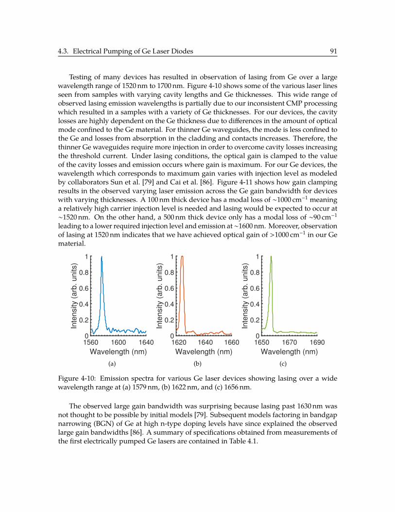
4.3. Electrical Pumping of Ge Laser Diodes 91
Testing of many devices has resulted in observation of lasing from Ge over a large
wavelength range of 1520 nm to 1700 nm. Figure 4-10 shows some of the various laser lines
seen from samples with varying cavity lengths and Ge thicknesses. This wide range of
observed lasing emission wavelengths is partially due to our inconsistent CMP processing
which resulted in a samples with a variety of Ge thicknesses. For our devices, the cavity
losses are highly dependent on the Ge thickness due to differences in the amount of optical
mode confined to the Ge material. For thinner Ge waveguides, the mode is less confined to
the Ge and losses from absorption in the cladding and contacts increases. Therefore, the
thinner Ge waveguides require more injection in order to overcome cavity losses increasing
the threshold current. Under lasing conditions, the optical gain is clamped to the value
of the cavity losses and emission occurs where gain is maximum. For our Ge devices, the
wavelength which corresponds to maximum gain varies with injection level as modeled
by collaborators Sun et al. [79] and Cai et al. [86]. Figure 4-11 shows how gain clamping
results in the observed varying laser emission across the Ge gain bandwidth for devices
with varying thicknesses. A 100 nm thick device has a modal loss of ∼1000 cm−1
meaning
a relatively high carrier injection level is needed and lasing would be expected to occur at
∼1520 nm. On the other hand, a 500 nm thick device only has a modal loss of ∼90 cm−1
leading to a lower required injection level and emission at∼1600 nm. Moreover, observation
of lasing at 1520 nm indicates that we have achieved optical gain of >1000 cm−1
in our Ge
material.
Wavelength (nm)
1560 1600 1640
Inte
nsity (
arb
. units)
0
0.2
0.4
0.6
0.8
1
(a)
Wavelength (nm)
1620 1640 1660
Inte
nsity (
arb
. units)
0
0.2
0.4
0.6
0.8
1
(b)
Wavelength (nm)
1650 1670 1690
Inte
nsity (
arb
. units)
0
0.2
0.4
0.6
0.8
1
(c)
Figure 4-10: Emission spectra for various Ge laser devices showing lasing over a wide
wavelength range at (a) 1579 nm, (b) 1622 nm, and (c) 1656 nm.
The observed large gain bandwidth was surprising because lasing past 1630 nm was
not thought to be possible by initial models [79]. Subsequent models factoring in bandgap
narrowing (BGN) of Ge at high n-type doping levels have since explained the observed
large gain bandwidths [86]. A summary of specifications obtained from measurements of
the first electrically pumped Ge lasers are contained in Table 4.1.
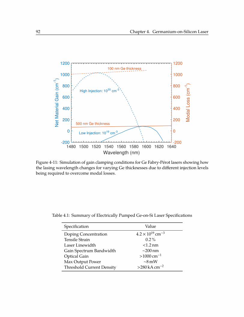
92 Chapter 4. Germanium-on-Silicon Laser
1480 1500 1520 1540 1560 1580 1600 1620 1640
Wavelength (nm)
-200
0
200
400
600
800
1000
1200
Ne
t M
ate
ria
l G
ain
(cm
-1)
-200
0
200
400
600
800
1000
1200
Mo
da
l L
oss (
cm
-1)
High Injection: 1020 cm-3
Low Injection: 1019 cm-3
100 nm Ge thickness
500 nm Ge thickness
Figure 4-11: Simulation of gain clamping conditions for Ge Fabry-Pérot lasers showing how
the lasing wavelength changes for varying Ge thicknesses due to different injection levels
being required to overcome modal losses.
Table 4.1: Summary of Electrically Pumped Ge-on-Si Laser Specifications
Specification Value
Doping Concentration 4.2 × 10¹⁹
cm−3
Tensile Strain 0.2 %
Laser Linewidth <1.2 nm
Gain Spectrum Bandwidth ∼200 nm
Optical Gain >1000 cm−1
Max Output Power ∼8 mW
Threshold Current Density >280 kA cm−2
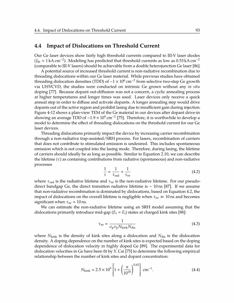
4.4. Impact of Dislocations on Threshold Current 93
4.4 Impact of Dislocations on Threshold CurrentOur Ge laser devices show fairly high threshold currents compared to III-V laser diodes
(Jth ≈ 1 kA cm−2
). Modeling has predicted that threshold currents as low as 0.53 kA cm−2
(comparable to III-V lasers) should be achievable from a double heterojunction Ge laser [86].
A potential source of increased threshold current is non-radiative recombination due to
threading dislocations within our Ge laser material. While previous studies have obtained
threading dislocation densities (TDD) of ∼1 × 10⁶
cm−2
from selective two-step Ge growth
via UHVCVD, the studies were conducted on intrinsic Ge grown without any in situdoping [77]. Because dopant out-diffusion was not a concern, a cyclic annealing process
at higher temperatures and longer times was used. Laser devices only receive a quick
anneal step in order to diffuse and activate dopants. A longer annealing step would drive
dopants out of the active region and prohibit lasing due to insufficient gain during injection.
Figure 4-12 shows a plan-view TEM of the Ge material in our devices after dopant drive-in
showing an average TDD of ∼1.9 × 10⁹
cm−2
[75]. Therefore, it is worthwhile to develop a
model to determine the effect of threading dislocations on the threshold current for our Ge
laser devices.
Threading dislocations primarily impact the device by increasing carrier recombination
through a non-radiative trap-assisted/SRH process. For lasers, recombination of carriers
that does not contribute to stimulated emission is undesired. This includes spontaneous
emission which is not coupled into the lasing mode. Therefore, during lasing, the lifetime
of carriers should ideally be as long as possible. Similar to Equation 2.10, we can describe
the lifetime (τ) as containing contributions from radiative (spontaneous) and non-radiative
processes
1
τ
1
τrad
+1
τnr
(4.2)
where τrad is the radiative lifetime and τnr is the non-radiative lifetime. For our pseudo-
direct bandgap Ge, the direct transition radiative lifetime is ∼ 10 ns [87]. If we assume
that non-radiative recombination is dominated by dislocations, based on Equation 4.2, the
impact of dislocations on the overall lifetime is negligible when τnr 10 ns and becomes
significant when τnr ≈ 10 ns.
We can estimate the non-radiative lifetime using an SRH model assuming that the
dislocations primarily introduce mid-gap (Et Ei) states at charged kink sites [88]:
τnr 1
σpvpNkinkNdis
(4.3)
where Nkink is the density of kink sites along a dislocation and Ndis is the dislocation
density. A doping dependence on the number of kink sites is expected based on the doping
dependence of dislocation velocity in highly doped Ge [89]. The experimental data for
dislocation velocities in Ge have been fit by Y. Cai [75] to determine the following empirical
relationship between the number of kink sites and dopant concentration:
Nkink 2.5 × 10⁵
1 +
(n
1018
)0.63
cm−1. (4.4)

94 Chapter 4. Germanium-on-Silicon Laser
Figure 4-12: Plan-view TEM of the Ge material in laser devices after dopant drive-in
thermal treatment of 750C for 1 min showing an average threading dislocation density of
∼1.9 × 10⁹
cm−2
. Courtesy of T. Milakovich [75]
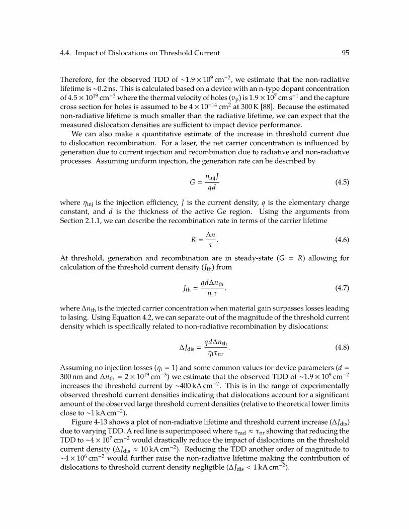
4.4. Impact of Dislocations on Threshold Current 95
Therefore, for the observed TDD of ∼1.9 × 10⁹
cm−2
, we estimate that the non-radiative
lifetime is ∼0.2 ns. This is calculated based on a device with an n-type dopant concentration
of 4.5 × 10¹⁹
cm−3
where the thermal velocity of holes (vp) is 1.9 × 10⁷
cm s−1
and the capture
cross section for holes is assumed to be 4 × 10⁻¹⁴
cm2
at 300 K [88]. Because the estimated
non-radiative lifetime is much smaller than the radiative lifetime, we can expect that the
measured dislocation densities are sufficient to impact device performance.
We can also make a quantitative estimate of the increase in threshold current due
to dislocation recombination. For a laser, the net carrier concentration is influenced by
generation due to current injection and recombination due to radiative and non-radiative
processes. Assuming uniform injection, the generation rate can be described by
G ηinj Jqd
(4.5)
where ηinj is the injection efficiency, J is the current density, q is the elementary charge
constant, and d is the thickness of the active Ge region. Using the arguments from
Section 2.1.1, we can describe the recombination rate in terms of the carrier lifetime
R ∆nτ. (4.6)
At threshold, generation and recombination are in steady-state (G R) allowing for
calculation of the threshold current density (Jth) from
Jth qd∆nth
ηiτ. (4.7)
where∆nth is the injected carrier concentration when material gain surpasses losses leading
to lasing. Using Equation 4.2, we can separate out of the magnitude of the threshold current
density which is specifically related to non-radiative recombination by dislocations:
∆Jdis qd∆nth
ηiτnr. (4.8)
Assuming no injection losses (ηi 1) and some common values for device parameters (d
300 nm and ∆nth 2 × 10¹⁹
cm−3
) we estimate that the observed TDD of ∼1.9 × 10⁹
cm−2
increases the threshold current by ∼400 kA cm−2
. This is in the range of experimentally
observed threshold current densities indicating that dislocations account for a significant
amount of the observed large threshold current densities (relative to theoretical lower limits
close to ∼1 kA cm−2
).
Figure 4-13 shows a plot of non-radiative lifetime and threshold current increase (∆Jdis)
due to varying TDD. A red line is superimposed where τrad ≈ τnr showing that reducing the
TDD to ∼4 × 10⁷
cm−2
would drastically reduce the impact of dislocations on the threshold
current density (∆Jdis ≈ 10 kA cm−2
). Reducing the TDD another order of magnitude to
∼4 × 10⁶
cm−2
would further raise the non-radiative lifetime making the contribution of
dislocations to threshold current density negligible (∆Jdis < 1 kA cm−2
).
96 Chapter 4. Germanium-on-Silicon Laser
107
108
109
Threading Dislocation Density (cm-2
)
0
10
20
30
40
50
No
n-r
ad
iative
Life
tim
e (
ns)
0
50
100
150
200
250
Thre
shold
Curr
ent In
cre
ase (
kA
/cm
2)
τrad
Figure 4-13: Estimation of non-radiative lifetimes and threshold current increases due to
varying threading dislocation densities. Non-radiative lifetime is approximately equal to
the radiative lifetime for a TDD of ∼4 × 10⁷
cm−2
.
4.5 Future WorkWe have successfully demonstrated electrically pumped lasing from Ge. Tested devices
have fairly high threshold currents which we have determined to largely be a result of the
high TDD in the active region. Further studies should focus on reducing the TDD in order
to reduce the threshold current density and increase the output power. If failure is indeed
related to the high threshold current, reducing TDD should also lead to increased reliability
of Ge lasers which is crucial for these devices to ever be used in a commercial application.
Furthermore, it is also possible that the recombination of carriers at dislocations is leading
to enhanced defect reactions also contributing to device failure (Section 2.2.2).
Reducing the TDD will be challenging, but as previously mentioned, desired values
(∼4 × 10⁶
cm−2
for negligible impact to threshold current density) have been achieved in
lower doped Ge grown via two-step UHVCVD. Potentially, additional annealing processes
could be developed which reduce the TDD before doping or delta doping of Ge.
In addition to reducing TDD, there are two obvious areas of improvement in our Ge
laser devices:
1. Non-optimal cavity design. In our work, Fabry-Pérot cavities were used to simplify
fabrication and testing. These structures were not completely optimized for reducing
modal overlap with the heavily doped Si layers and metal contacts. Moreover, one of
the mirrors was formed simply by cleaving of the samples. Better optimization of the
laser structure should lead to greatly reduced modal losses and mirror losses.
2. Severe dishing of Ge due to poor CMP. As previously mentioned, CMP of the Ge
after delta doping was not well controlled and lead to dishing of the Ge altering

4.5. Future Work 97
the supported modes and possibly increasing carrier recombination at the surface.
Subsequent CMP process optimization has lead to a Ge CMP procedure with much
better uniformity and control [90].
These factors largely influence ∆nth meaning that they could also lead to further reductions
in threshold current.

98 Chapter 4. Germanium-on-Silicon Laser
Chapter 5
Colloidal Quantum Dot ChalcogenideGlass Films
Integrated light sources are also a key component for enabling the fabrication of small-
footprint, high sensitivity system-on-chip optical based chem-bio sensors. For optical
sensing schemes, the optical path length determines the overall sensitivity and ideally
should be as large as possible. However, for a tabletop spectrometer, this requires increasing
the overall footprint of the system. Using microphotonic resonators on chip, the path length
can be increased significantly while simultaneously reducing the overall footprint of the
system through integration of components (e.g., sensing elements, photodetectors, and
read-out circuitry). The drastic reduction in the size of sensor systems can enable novel
applications where real-time constant monitoring is needed.
Excluding the light source, a variety of components required for fabrication of system-
on-chip optical based chem-bio sensors have been fabricated for silicon and chalcogenide
glass platforms [5]. Optical resonator sensors can operate in two modes of sensing, each
based on observing changes in a different component of the complex refractive index
(Figure 5-1). Cavity-enhanced absorption spectroscopy (absorption sensing), relies on
measurement of extinction ratio changes in a resonant peak due to optical absorption by
the analyte [91]. Chemicals can be identified by their "fingerprint" in the mid-IR due to
absorption by molecular vibrational modes. Refractive index spectoscopy (index sensing)
instead correlates a shift in resonant peak wavelength to a change in effective index resulting
from the presence of the analyte being sensed [92, 93]. In this sensing mode, the signal is
often increased through the use of a functional layer which reacts with the analyte creating a
larger shift in the effective index than would been seen by the presence of the analyte alone.
The choice of source wavelength is less restrictive than for cavity-enhanced absorption
spectroscopy.
In this chapter, we investigate the optical properties and morphology of thin films
containing colloidal quantum dots incorporated into a chalcogenide glass matrix. Unlike
The work in this chapter was done in collaboration with Prof. Moungi Bawendi’s group at MIT (synthesis and
preparation of quantum dots) and Prof. Kathleen Richardson’s group formerly at Clemson University now at
University of Central Florida (synthesis of bulk chalcogenide glasses) with mentorship from Prof. Clara Dimas
at Masdar Institute of Science and Techonology.
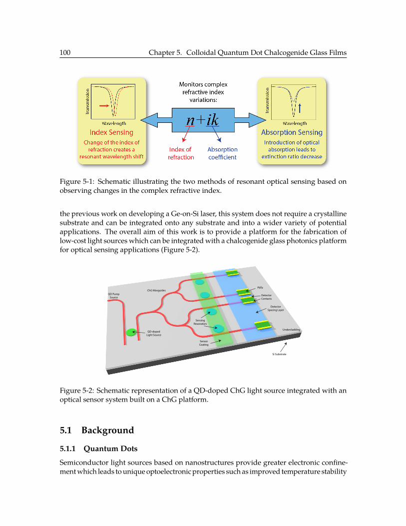
100 Chapter 5. Colloidal Quantum Dot Chalcogenide Glass Films
Figure 5-1: Schematic illustrating the two methods of resonant optical sensing based on
observing changes in the complex refractive index.
the previous work on developing a Ge-on-Si laser, this system does not require a crystalline
substrate and can be integrated onto any substrate and into a wider variety of potential
applications. The overall aim of this work is to provide a platform for the fabrication of
low-cost light sources which can be integrated with a chalcogenide glass photonics platform
for optical sensing applications (Figure 5-2).
QD-dopedLight Source
SensorCoating
ChG Wavguides
SensingResonators
DetectorSpacing Layer
PbTe
DetectorContacts
QD PumpSource
Undercladding
Si Substrate
Figure 5-2: Schematic representation of a QD-doped ChG light source integrated with an
optical sensor system built on a ChG platform.
5.1 Background
5.1.1 Quantum Dots
Semiconductor light sources based on nanostructures provide greater electronic confine-
ment which leads to unique optoelectronic properties such as improved temperature stability
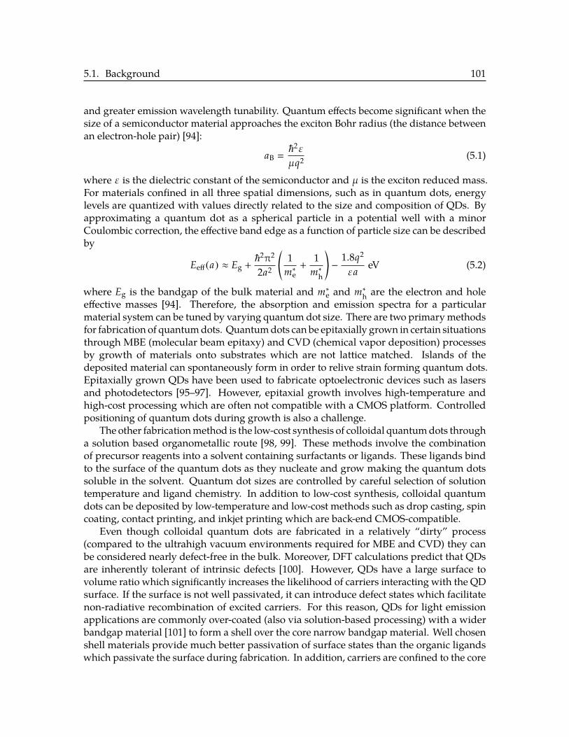
5.1. Background 101
and greater emission wavelength tunability. Quantum effects become significant when the
size of a semiconductor material approaches the exciton Bohr radius (the distance between
an electron-hole pair) [94]:
aB ~2ε
µq2
(5.1)
where ε is the dielectric constant of the semiconductor and µ is the exciton reduced mass.
For materials confined in all three spatial dimensions, such as in quantum dots, energy
levels are quantized with values directly related to the size and composition of QDs. By
approximating a quantum dot as a spherical particle in a potential well with a minor
Coulombic correction, the effective band edge as a function of particle size can be described
by
Eeff(a) ≈ Eg +~2π2
2a2
*,
1
m∗e
+1
m∗h
+-−
1.8q2
εaeV (5.2)
where Eg is the bandgap of the bulk material and m∗e
and m∗h
are the electron and hole
effective masses [94]. Therefore, the absorption and emission spectra for a particular
material system can be tuned by varying quantum dot size. There are two primary methods
for fabrication of quantum dots. Quantum dots can be epitaxially grown in certain situations
through MBE (molecular beam epitaxy) and CVD (chemical vapor deposition) processes
by growth of materials onto substrates which are not lattice matched. Islands of the
deposited material can spontaneously form in order to relive strain forming quantum dots.
Epitaxially grown QDs have been used to fabricate optoelectronic devices such as lasers
and photodetectors [95–97]. However, epitaxial growth involves high-temperature and
high-cost processing which are often not compatible with a CMOS platform. Controlled
positioning of quantum dots during growth is also a challenge.
The other fabrication method is the low-cost synthesis of colloidal quantum dots through
a solution based organometallic route [98, 99]. These methods involve the combination
of precursor reagents into a solvent containing surfactants or ligands. These ligands bind
to the surface of the quantum dots as they nucleate and grow making the quantum dots
soluble in the solvent. Quantum dot sizes are controlled by careful selection of solution
temperature and ligand chemistry. In addition to low-cost synthesis, colloidal quantum
dots can be deposited by low-temperature and low-cost methods such as drop casting, spin
coating, contact printing, and inkjet printing which are back-end CMOS-compatible.
Even though colloidal quantum dots are fabricated in a relatively “dirty” process
(compared to the ultrahigh vacuum environments required for MBE and CVD) they can
be considered nearly defect-free in the bulk. Moreover, DFT calculations predict that QDs
are inherently tolerant of intrinsic defects [100]. However, QDs have a large surface to
volume ratio which significantly increases the likelihood of carriers interacting with the QD
surface. If the surface is not well passivated, it can introduce defect states which facilitate
non-radiative recombination of excited carriers. For this reason, QDs for light emission
applications are commonly over-coated (also via solution-based processing) with a wider
bandgap material [101] to form a shell over the core narrow bandgap material. Well chosen
shell materials provide much better passivation of surface states than the organic ligands
which passivate the surface during fabrication. In addition, carriers are confined to the core
102 Chapter 5. Colloidal Quantum Dot Chalcogenide Glass Films
providing shielding from the potentially weaker passivation at the outer shell surface.
Using various materials systems, colloidal quantum dots have be fabricated which
emit from ultraviolet [102] to mid-IR regimes [103, 104]. Previous studies have shown
demonstration of lasing from colloidal quantum dots coupled to microspheres [105, 106]
and microcapillary tubes [107, 108]. However, these device designs are not suitable for
integration with other components hindering their application in photonic circuit applica-
tions. In this work we will focus on infrared sources for the reasons outlined earlier with
the overall goal of developing a light source which can be integrated with other photonic
components. Studies of IR emitters show that a strong quantum confinement regime can
be achieved by narrow-bandgap IV–VI QDs (e.g., PbS and PbSe) due to large electron, hole,
and exciton Bohr radii in IV–VI semiconductors compared with II–VI or III–V materials [109,
110]. Although mid-IR emission out to 4.1 µm has been shown for PbSe quantum dots,
the quantum yields are significantly reduced from near-unity for near-IR quantum dots
to .10 % for mid-IR emitting PbSe quantum dots [103]. The synthesis of well passivated
mid-infrared quantum dots is still an outstanding problem. In this work, we use PbS
quantum dots overcoated with CdS shells (Figure 5-3) which emit efficiently in the near-IR
in order to reduce any possible issues related to poor quantum yields. However, our goal
is to develop a platform for making light sources through incorporation of quantum dots
into chalcogenide glasses and is largely independent of the specific quantum dot material
used. This work can potentially be replicated with other quantum dot systems to produce
light sources which emit from the UV to the mid-IR regimes.
Figure 5-3: Schematic of PbS colloidal quantum dot synthesis through hot injection.
Bis(trimethylsilyl)sulfide intrioctylphosphine is quickly injected into a carefully temper-
ature controlled precursor solution containing PbO and oleic acid. The PbO reduces and
reacts to nucleate PbS QDs whose growth quickly self terminates through passivation of
the QDs by oleic acid ligands. Further materials can be added to the solution after QD
nucleation to grow semiconductor shells to tailor electronic properties and provide extra
surface passivation.

5.1. Background 103
5.1.2 Chalcogenide Glasses
Chalcogenide glasses (ChGs) are amorphous compounds composed of metals and non-
metals bonded with chalcogen elements (sulfur, selenium, and tellurium). Due to their phase
change properties, ChGs have been used in non-volatile memory applications for a number
of years [111, 112]. More recently, ChGs have found applications in microphotonic systems
due to a number of desirable optical properties. ChGs have a wide optical transparency
window encompassing visible to far infrared regimes [113]. This makes them a promising
material for chemical sensing applications because many of the vibration absorption lines
for molecules lie in the mid-infrared [5] where silicon-on-insulator (SOI) systems are
lossy [114]. The index of refraction for ChGs can be tuned by variation of element choice
and composition. In addition, the index of refraction is relatively high (n ≈ 2–3) allowing
for greater confinement in photonic circuit elements. This has the benefit of reducing the
overall footprint of ChG photonic circuits. The wide tunablility of ChGs also allows for index
contrasts as high as ∆n > 1 from a single ChG alloy system. Previous studies have already
shown potential for ChG photonics by successful demonstration of low loss waveguides
and high quality factor (high-Q) resonator cavities using ChG materials [115–117].
One of the greatest advantages to using a ChG platform for photonics applications is
that their amoprhous nature allows for low temperature deposition of thin films on most
substrates regardless of substrate lattice constant. This facilitates easy integration of ChG
components with other photonic components and materials platforms (including being Si
CMOS-backend compatible). ChGs can be deposited by a number of different deposition
techniques including thermal evaporation, chemical vapor deposition (CVD), pulsed laser
deposition (PLD), and RF magnetron sputtering. Our collaborators at Clemson University
have developed an alternative method where bulk ChGs are dissolved and deposited
through solution based techniques such as drop casting and spin coating [118]. We have
primarily focused on using two ChG compositions which can be solution-processed: As2S3
and Ge23Sb7S70. The experiments carried out in this section have been performed using
both ChG compositions.
The general procedure for deposition of ChG thin films by spin coating used in this
work is as follows:
1. Bulk ChGs are prepared by our collaborators at Clemson University using a traditional
melt-quench technique starting with high purity elemental constituents. Materials
are vacuum sealed inside quartz ampoules and heated to several hundred degrees
Celsius for several hours in a rocking furnace. The ampoule is air-quenched and
subsequently annealed at sub glass transition (Tg) temperatures.
2. In order to accelerate the dissolution process, mortar and pestle are used to crush the
bulk glass into particles ∼1 mm in diameter.
3. Crushed glass is added to the solvent in a small vial with a stir bar. The vial is
sealed to prevent solvent evaporation and the mixture is stirred for ∼2 days in order
to completely dissolve the ChG. Because dissolution is altered by the presence of
moisture, solution processing of ChGs is carried out inside a glovebox where H2O
and O2 are removed by circulation of the inert N2 atmosphere over a copper catalyst
bed.
4. Solutions are filtered through a 0.1 µm syringe filter and spun onto substrates with
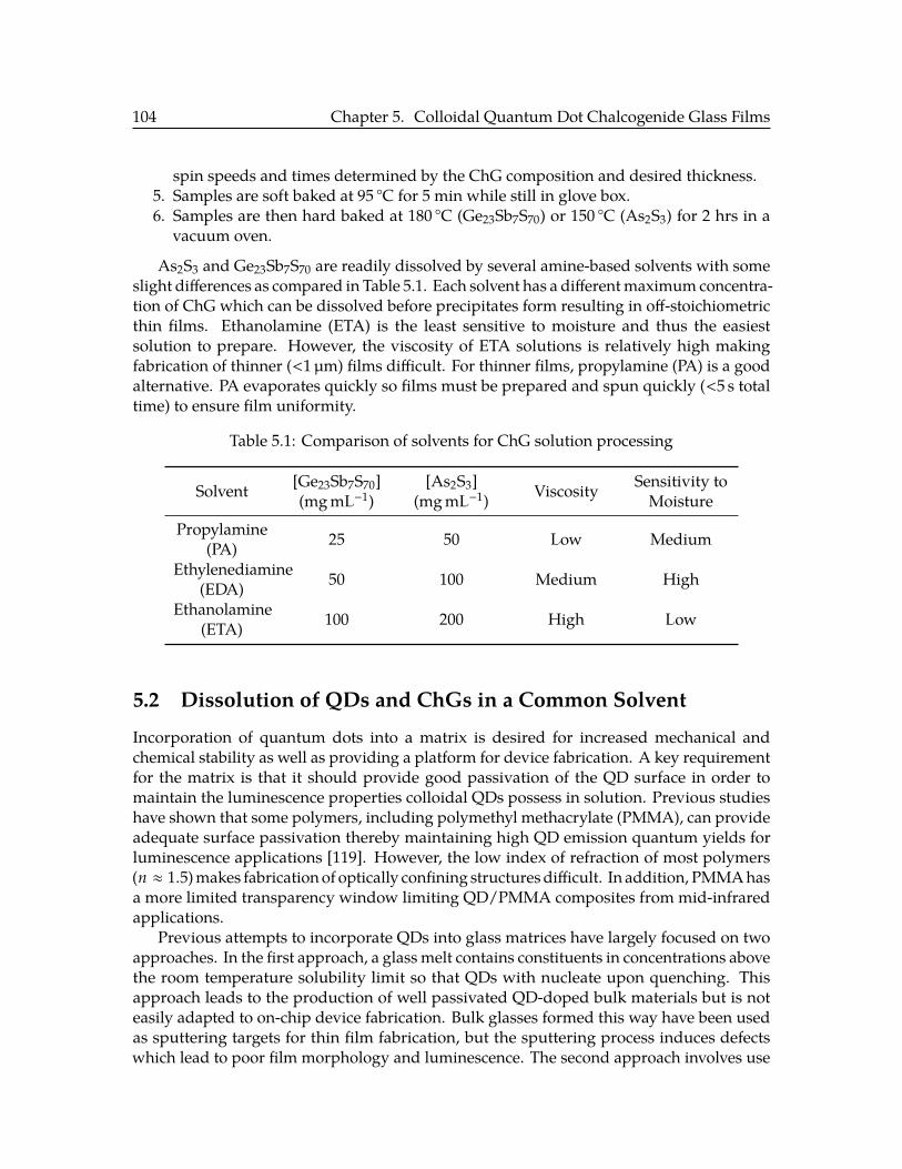
104 Chapter 5. Colloidal Quantum Dot Chalcogenide Glass Films
spin speeds and times determined by the ChG composition and desired thickness.
5. Samples are soft baked at 95C for 5 min while still in glove box.
6. Samples are then hard baked at 180C (Ge23Sb7S70) or 150
C (As2S3) for 2 hrs in a
vacuum oven.
As2S3 and Ge23Sb7S70 are readily dissolved by several amine-based solvents with some
slight differences as compared in Table 5.1. Each solvent has a different maximum concentra-
tion of ChG which can be dissolved before precipitates form resulting in off-stoichiometric
thin films. Ethanolamine (ETA) is the least sensitive to moisture and thus the easiest
solution to prepare. However, the viscosity of ETA solutions is relatively high making
fabrication of thinner (<1 µm) films difficult. For thinner films, propylamine (PA) is a good
alternative. PA evaporates quickly so films must be prepared and spun quickly (<5 s total
time) to ensure film uniformity.
Table 5.1: Comparison of solvents for ChG solution processing
Solvent
[Ge23Sb7S70]
(mg mL−1
)
[As2S3]
(mg mL−1
)
Viscosity
Sensitivity to
Moisture
Propylamine
(PA)
25 50 Low Medium
Ethylenediamine
(EDA)
50 100 Medium High
Ethanolamine
(ETA)
100 200 High Low
5.2 Dissolution of QDs and ChGs in a Common SolventIncorporation of quantum dots into a matrix is desired for increased mechanical and
chemical stability as well as providing a platform for device fabrication. A key requirement
for the matrix is that it should provide good passivation of the QD surface in order to
maintain the luminescence properties colloidal QDs possess in solution. Previous studies
have shown that some polymers, including polymethyl methacrylate (PMMA), can provide
adequate surface passivation thereby maintaining high QD emission quantum yields for
luminescence applications [119]. However, the low index of refraction of most polymers
(n ≈ 1.5) makes fabrication of optically confining structures difficult. In addition, PMMA has
a more limited transparency window limiting QD/PMMA composites from mid-infrared
applications.
Previous attempts to incorporate QDs into glass matrices have largely focused on two
approaches. In the first approach, a glass melt contains constituents in concentrations above
the room temperature solubility limit so that QDs with nucleate upon quenching. This
approach leads to the production of well passivated QD-doped bulk materials but is not
easily adapted to on-chip device fabrication. Bulk glasses formed this way have been used
as sputtering targets for thin film fabrication, but the sputtering process induces defects
which lead to poor film morphology and luminescence. The second approach involves use
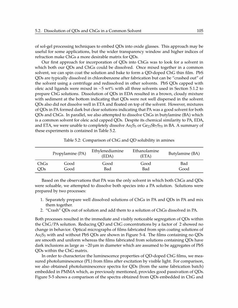
5.2. Dissolution of QDs and ChGs in a Common Solvent 105
of sol-gel processing techniques to embed QDs into oxide glasses. This approach may be
useful for some applications, but the wider transparency window and higher indices of
refraction make ChGs a more desirable matrix for QDs.
Our first approach for incorporation of QDs into ChGs was to look for a solvent in
which both our QDs and ChGs could be dissolved. Once mixed together in a common
solvent, we can spin coat the solution and bake to form a QD-doped ChG thin film. PbS
QDs are typically dissolved in chlorobenzene after fabrication but can be “crashed out” of
the solvent using a centrifuge and redissolved in other solvents. PbS QDs capped with
oleic acid ligands were mixed in ∼5 wt% with all three solvents used in Section 5.1.2 to
prepare ChG solutions. Dissolution of QDs in EDA resulted in a brown, cloudy mixture
with sediment at the bottom indicating that QDs were not well dispersed in the solvent.
QDs also did not dissolve well in ETA and floated on top of the solvent. However, mixtures
of QDs in PA formed dark but clear solutions indicating that PA was a good solvent for both
QDs and ChGs. In parallel, we also attempted to dissolve ChGs in butylamine (BA) which
is a common solvent for oleic acid capped QDs. Despite its chemical similarity to PA, EDA,
and ETA, we were unable to completely dissolve As2S3 or Ge23Sb7S70 in BA. A summary of
these experiments is contained in Table 5.2.
Table 5.2: Comparison of ChG and QD solubility in amines
Propylamine (PA)
Ethylenediamine
(EDA)
Ethanolamine
(ETA)
Butylamine (BA)
ChGs Good Good Good Bad
QDs Good Bad Bad Good
Based on the observations that PA was the only solvent in which both ChGs and QDs
were soluable, we attempted to dissolve both species into a PA solution. Solutions were
prepared by two processes:
1. Separately prepare well dissolved solutions of ChGs in PA and QDs in PA and mix
them together.
2. “Crash” QDs out of solution and add them to a solution of ChGs dissolved in PA.
Both processes resulted in the immediate and visibly noticeable segregation of QDs within
the ChG/PA solution. Reducing QD and ChG concentrations by a factor of 2 showed no
change in behavior. Optical micrographs of films fabricated from spin coating solutions of
As2S3 with and without PbS QDs are shown in Figure 5-4. The films containing no QDs
are smooth and uniform whereas the films fabricated from solutions containing QDs have
dark inclusions as large as ∼20 µm in diameter which are assumed to be aggregates of PbS
QDs within the ChG matrix.
In order to characterize the luminescence properties of QD-doped ChG films, we mea-
sured photoluminescence (PL) from films after excitation by visible light. For comparison,
we also obtained photoluminescence spectra for QDs (from the same fabrication batch)
embedded in PMMA which, as previously mentioned, provides good passivation of QDs.
Figure 5-5 shows a comparison of the spectra obtained from QDs embedded in ChG and
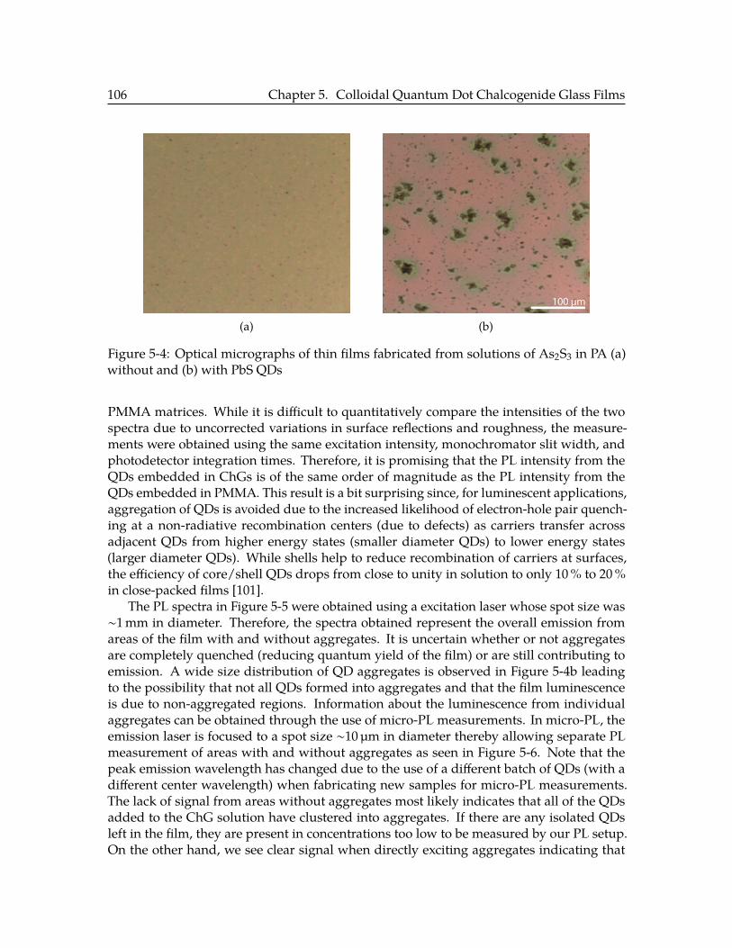
106 Chapter 5. Colloidal Quantum Dot Chalcogenide Glass Films
(a) (b)
Figure 5-4: Optical micrographs of thin films fabricated from solutions of As2S3 in PA (a)
without and (b) with PbS QDs
PMMA matrices. While it is difficult to quantitatively compare the intensities of the two
spectra due to uncorrected variations in surface reflections and roughness, the measure-
ments were obtained using the same excitation intensity, monochromator slit width, and
photodetector integration times. Therefore, it is promising that the PL intensity from the
QDs embedded in ChGs is of the same order of magnitude as the PL intensity from the
QDs embedded in PMMA. This result is a bit surprising since, for luminescent applications,
aggregation of QDs is avoided due to the increased likelihood of electron-hole pair quench-
ing at a non-radiative recombination centers (due to defects) as carriers transfer across
adjacent QDs from higher energy states (smaller diameter QDs) to lower energy states
(larger diameter QDs). While shells help to reduce recombination of carriers at surfaces,
the efficiency of core/shell QDs drops from close to unity in solution to only 10 % to 20 %
in close-packed films [101].
The PL spectra in Figure 5-5 were obtained using a excitation laser whose spot size was
∼1 mm in diameter. Therefore, the spectra obtained represent the overall emission from
areas of the film with and without aggregates. It is uncertain whether or not aggregates
are completely quenched (reducing quantum yield of the film) or are still contributing to
emission. A wide size distribution of QD aggregates is observed in Figure 5-4b leading
to the possibility that not all QDs formed into aggregates and that the film luminescence
is due to non-aggregated regions. Information about the luminescence from individual
aggregates can be obtained through the use of micro-PL measurements. In micro-PL, the
emission laser is focused to a spot size ∼10 µm in diameter thereby allowing separate PL
measurement of areas with and without aggregates as seen in Figure 5-6. Note that the
peak emission wavelength has changed due to the use of a different batch of QDs (with a
different center wavelength) when fabricating new samples for micro-PL measurements.
The lack of signal from areas without aggregates most likely indicates that all of the QDs
added to the ChG solution have clustered into aggregates. If there are any isolated QDs
left in the film, they are present in concentrations too low to be measured by our PL setup.
On the other hand, we see clear signal when directly exciting aggregates indicating that
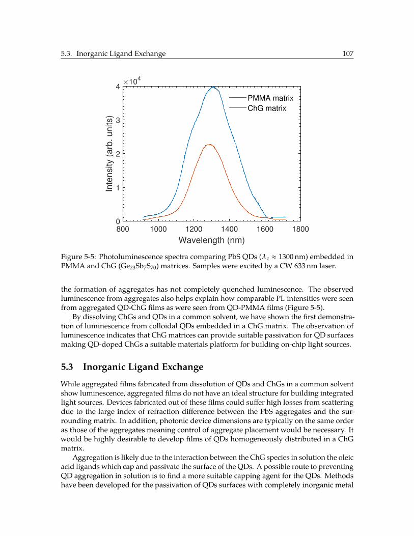
5.3. Inorganic Ligand Exchange 107
Wavelength (nm)
800 1000 1200 1400 1600 1800
Inte
nsity (
arb
. u
nits)
×104
0
1
2
3
4
PMMA matrix
ChG matrix
Figure 5-5: Photoluminescence spectra comparing PbS QDs (λc ≈ 1300 nm) embedded in
PMMA and ChG (Ge23Sb7S70) matrices. Samples were excited by a CW 633 nm laser.
the formation of aggregates has not completely quenched luminescence. The observed
luminescence from aggregates also helps explain how comparable PL intensities were seen
from aggregated QD-ChG films as were seen from QD-PMMA films (Figure 5-5).
By dissolving ChGs and QDs in a common solvent, we have shown the first demonstra-
tion of luminescence from colloidal QDs embedded in a ChG matrix. The observation of
luminescence indicates that ChG matrices can provide suitable passivation for QD surfaces
making QD-doped ChGs a suitable materials platform for building on-chip light sources.
5.3 Inorganic Ligand ExchangeWhile aggregated films fabricated from dissolution of QDs and ChGs in a common solvent
show luminescence, aggregated films do not have an ideal structure for building integrated
light sources. Devices fabricated out of these films could suffer high losses from scattering
due to the large index of refraction difference between the PbS aggregates and the sur-
rounding matrix. In addition, photonic device dimensions are typically on the same order
as those of the aggregates meaning control of aggregate placement would be necessary. It
would be highly desirable to develop films of QDs homogeneously distributed in a ChG
matrix.
Aggregation is likely due to the interaction between the ChG species in solution the oleic
acid ligands which cap and passivate the surface of the QDs. A possible route to preventing
QD aggregation in solution is to find a more suitable capping agent for the QDs. Methods
have been developed for the passivation of QDs surfaces with completely inorganic metal
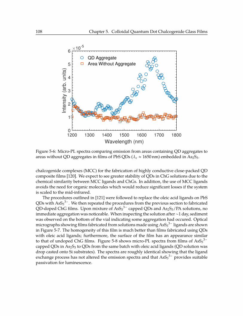
108 Chapter 5. Colloidal Quantum Dot Chalcogenide Glass Films
Wavelength (nm)
1200 1300 1400 1500 1600 1700 1800
Inte
nsity (
arb
. u
nits)
×10-5
0
1
2
3
4
5
6
QD Aggregate
Area Without Aggregate
Figure 5-6: Micro-PL spectra comparing emission from areas containing QD aggregates to
areas without QD aggregates in films of PbS QDs (λc ≈ 1650 nm) embedded in As2S3.
chalcogenide complexes (MCC) for the fabrication of highly conductive close-packed QD
composite films [120]. We expect to see greater stability of QDs in ChG solutions due to the
chemical similarity between MCC ligands and ChGs. In addition, the use of MCC ligands
avoids the need for organic molecules which would reduce significant losses if the system
is scaled to the mid-infrared.
The procedures outlined in [121] were followed to replace the oleic acid ligands on PbS
QDs with AsS3
3–
. We then repeated the procedures from the previous section to fabricated
QD-doped ChG films. Upon mixture of AsS3
3–
capped QDs and As2S3/PA solutions, no
immediate aggregation was noticeable. When inspecting the solution after∼1 day, sediment
was observed on the bottom of the vial indicating some aggregation had occured. Optical
micrographs showing films fabricated from solutions made using AsS3
3–
ligands are shown
in Figure 5-7. The homogeneity of this film is much better than films fabricated using QDs
with oleic acid ligands; furthermore, the surface of the film has an appearance similar
to that of undoped ChG films. Figure 5-8 shows micro-PL spectra from films of AsS3
3–
capped QDs in As2S3 to QDs from the same batch with oleic acid ligands (QD solution was
drop casted onto Si substrates). The spectra are roughly identical showing that the ligand
exchange process has not altered the emission spectra and that AsS3
3–
provides suitable
passivation for luminescence.
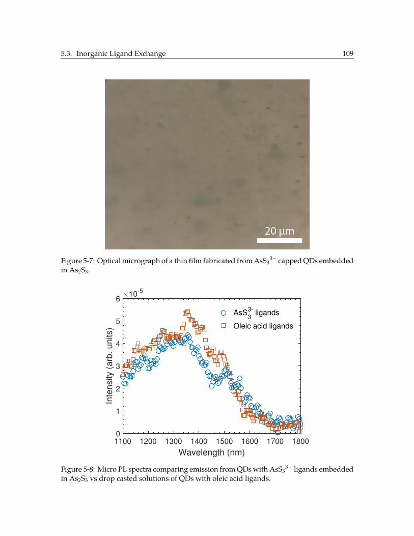
5.3. Inorganic Ligand Exchange 109
Figure 5-7: Optical micrograph of a thin film fabricated from AsS3
3–
capped QDs embedded
in As2S3.
Wavelength (nm)
1100 1200 1300 1400 1500 1600 1700 1800
Inte
nsity (
arb
. u
nits)
×10-5
0
1
2
3
4
5
6
AsS3
3- ligands
Oleic acid ligands
Figure 5-8: Micro PL spectra comparing emission from QDs with AsS3
3–
ligands embedded
in As2S3 vs drop casted solutions of QDs with oleic acid ligands.
110 Chapter 5. Colloidal Quantum Dot Chalcogenide Glass Films
5.4 Future WorkWe have demonstrated the feasibility of incorporating colloidal QDs into ChGs for light
source applications. ChGs are able to provide a mechanically robust, high index of refraction
matrix while adequately passivating the surface retaining the luminescent properties of QDs.
We have identified a pathway towards obtaining films with homogeneously distributed
QDs using mixing QDs with AsS3
3–
ligands into solutions of ChGs dissolved in PA. While
an inorganic ligand approach has yielded homogeneous films that are suitable for device
fabrication, we have observed some issues preventing its adoption for immediate use in
device fabrication:
1. Successful fabrication of uniform films is a low yield process. This is possibly due
to the process being very sensitive to the environment in which QDs are mixed with
ChGs. However, even when conditions are kept as similar as possible in a glovebox
which has low O2 and H2O concentrations, ∼50 % of the time, AsS3
3–
capped QDs
will aggregate when mixed with ChG solutions.
2. Solutions must be fabricated into films immediately. QDs are homogeneously dis-
tributed immediately after mixing of AsS3
3–
capped QDs with ChGs but will start
to aggregate soon after. Films fabricated from solutions made ∼1 day previously,
showed aggregates as large as ∼40 µm in diameter. These films also showed sig-
nificant red-shifting of emission spectra indicating that AsS3
3–
ligands allow easier
(relative to oleic acid) transfer of carriers from small QDs to large QDs. We expect
that this red shift would also be accompanied by a reduction in quantum yield but
have not attempted to experimentally verify that.
3. Even with films fabricated quickly after adding QDs to ChG solutions, stability is an
issue. We have observed a significant drop off of luminescence of films over time and
typically cannot measure any emission after ∼1 month.
The mechanism behind the observed instability and quenching is unknown at this time.
It is possible that the ChG matrix or remnant solvent in the matrix is reacting with the
inorganic ligands stripping them from the QDs. Another possibility is that the ligand
exchange process is incomplete and leaves unpassivated sites on the shell surface which
can be attacked by the matrix or solvent in the matrix. If AsS3
3–
capped QDs in ChGs are to
be used in practical devices, the mechanism behind quenching will need to be understood
and mitigated.
Chapter 6
Triplet Energy Transfer To Silicon
The impact on global climate change due to CO2 emissions from energy generation via
the burning of fossil fuels has created strong motivation for moving to alternative energy
sources [122]. Solar power holds promise for providing a large amount of clean and
sustainable energy. However, in 2014, solar power only accounted for 0.8 % (United States)
and 1.0 % (global) of all electricity generated [123]. High cost relative to other energy sources
is a large reason for poor adoption to date. In 2011, the U.S. Department of Energy launched
the SunShot initiative to reduce the cost of solar energy 75 % by 2020 which is predicted to
increase solar market penetration to 14 % by 2030 and 27 % by 2050 greatly reducing CO2
emissions by the electric-sector [124]. Currently, 91 % of the energy generated by solar cells
are based on silicon materials (either single crystalline or multi-crystalline) [123].
Silicon solar cell efficiency improvements can help play a role in reducing solar cell costs
and reaching those goals. Shockley and Queisser used a detailed balance calculation to
determine that Si single junction solar cells are limited to theoretical max efficiency of ∼32 %
which is very close to the maximum for any single junction solar cell [125]. Currently, the
best single junction silicon solar cells (non-concentrated) have efficiencies of ∼25 % [126]
with the difference largely being a result of recombination processes not accounted for in
the original detailed balance model [127]. The two largest loss mechanisms are (1) non-
absorption of photons with energies below the bandgap and (2) thermalization of carriers
to the band edges after absorption by photons with energies above the bandgap. Figure 6-1
shows a plot of the solar spectrum with the amount of power lost to these components
for a silicon solar cell. The fraction of the total power for a particular wavelength lost to
thermalization is superimposed to illustrate that for blue and green light, over 50 % of the
power is lost to thermalization.
One way to increase efficiencies by reducing thermalization losses is to build a multi-
junction solar cell which contains multiple semiconductors, each with a different bandgap.
The solar cell is structured so that each semiconductor absorbs the portion of the solar
spectrum where it is most efficient at power extraction. Multijunction solar cells have
been fabricated which show overall efficiencies >40 % [126]. However, due to difficulty of
fabrication, multijunction solar cells are very expensive and are primarily used in niche
applications where efficiency is valued above cost (e.g., satellites in space).
The experimental work in this chapter was done in collaboration with Prof. Marc Baldo’s group at MIT.
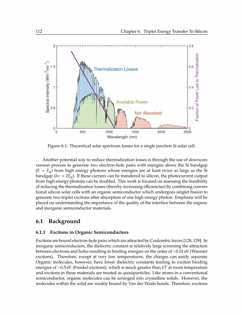
112 Chapter 6. Triplet Energy Transfer To Silicon
Wavelength (nm)
0 500 1000 1500 2000 2500
Spectr
al In
tensity (
Wm
-2nm
-1)
0
0.5
1
1.5
2
Fra
ction o
f P
ow
er
Lost to
Therm
aliz
ation
0
0.2
0.4
0.6
0.8
Not Absorbed
Thermalization Losses
Available Power
Figure 6-1: Theoretical solar spectrum losses for a single junction Si solar cell.
Another potential way to reduce thermalization losses is through the use of downcon-
version process to generate two electron-hole pairs with energies above the Si bandgap
(E > Eg) from high energy photons whose energies are at least twice as large as the Si
bandgap (hν > 2Eg). If these carriers can be transfered to silicon, the photocurrent output
from high energy photons can be doubled. This work is focused on assessing the feasibility
of reducing the thermalization losses (thereby increasing efficiencies) by combining conven-
tional silicon solar cells with an organic semiconductor which undergoes singlet fission to
generate two triplet excitons after absorption of one high energy photon. Emphasis will be
placed on understanding the importance of the quality of the interface between the organic
and inorganic semiconductor materials.
6.1 Background
6.1.1 Excitons in Organic Semiconductors
Excitons are bound electron-hole pairs which are attracted by Coulombic forces [128, 129]. In
inorganic semiconductors, the dielectric constant is relatively large screening the attraction
between electrons and holes resulting in binding energies on the order of ∼0.01 eV (Wannier
excitons). Therefore, except at very low temperatures, the charges can easily separate.
Organic molecules, however, have lower dielectric constants leading to exciton binding
energies of ∼0.5 eV (Frenkel excitons), which is much greater than kT at room temperature
and excitons in these materials are treated as quasiparticles. Like atoms in a conventional
semiconductor, organic molecules can be arranged into crystalline solids. However, the
molecules within the solid are weakly bound by Van der Waals bonds. Therefore, excitons
6.1. Background 113
in organic semiconductors are often localized to single (or a few at most) molecules.
The energy levels of organic molecular models are best described by molecular orbital
theory where molecules form a set of complex molecular orbitals which are filled by
electrons according to the Pauli exclusion principle. Let’s consider the creation of an exciton
by excitation of an electron from the highest occupied molecular orbital (HOMO) to the
lowest unoccupied molecular orbital (LUMO). An important feature of this two level system
containing two electrons is the total spin. In the lowest energy state, both electrons occupy
the HOMO and since they are fermions they cannot have the same spin. One has spin
s +1
2(represented by ↑) and the other has spin s −
1
2(represented by ↓) and the total
spin is zero (stot 0). For an excited state (one electron in HOMO and one in LUMO), there
is one anti-symmetric spin configuration where stotal 0 (referred to as a singlet state)
1√
2
(|↑↓〉 − |↓↑〉
)s 0 (singlet) (6.1)
and three symmetric spin configurations where stotal 1 (referred to as triplet states)
|↑↑〉
1√
2
(|↑↓〉 + |↓↑〉
)s 1 (triplet)
|↓↓〉
(6.2)
when accounting for the indistinguishability of electrons [130].
The distinction between singlet and triplet states is important because during interac-
tions with light, singlet states cannot couple into triplet states and vice versa (due to the
requirement that electric transition dipole moment be nonzero). Therefore, if the ground
state is a singlet (true for most materials including those involved in this work) then upon
absorption of a photon, the only allowed transition is into the excited singlet configuration
(and not into any of the three triplet configurations). The reciprocal is also true, meaning
that triplet states cannot relax to the singlet ground state and thus have long lifetimes. In
addition, because electrons are indistinguishable fermions and thus have exchange symme-
try, when the spin state is symmetric (triplet) the spatial component of the wavefunction is
anti-symmetric, and when the spin state is anti-symmetric (singlet) the spatial component
of the wavefuntion is symmetric. A consequence of an anti-symmetric spatial wavefuntion
for triplet states is a reduction in electron-electron repulsion which lowers the overall energy
of the state relative to the excited singlet state for most materials. The difference in energy
between excited singlet and triplet states depends on geometry and varies considerably
from molecule to molecule [131].
6.1.2 Singlet Exciton Fission
While transitions from an excited singlet state to a triplet state are forbidden and require
a spin flip, in materials where the singlet state energy is approximately twice as large as
the triplet state energy, both energy and spin conservation can be upheld by generation of
two triplet states (T1) from an excited singlet state (S1) and a ground singlet state (S0) in a
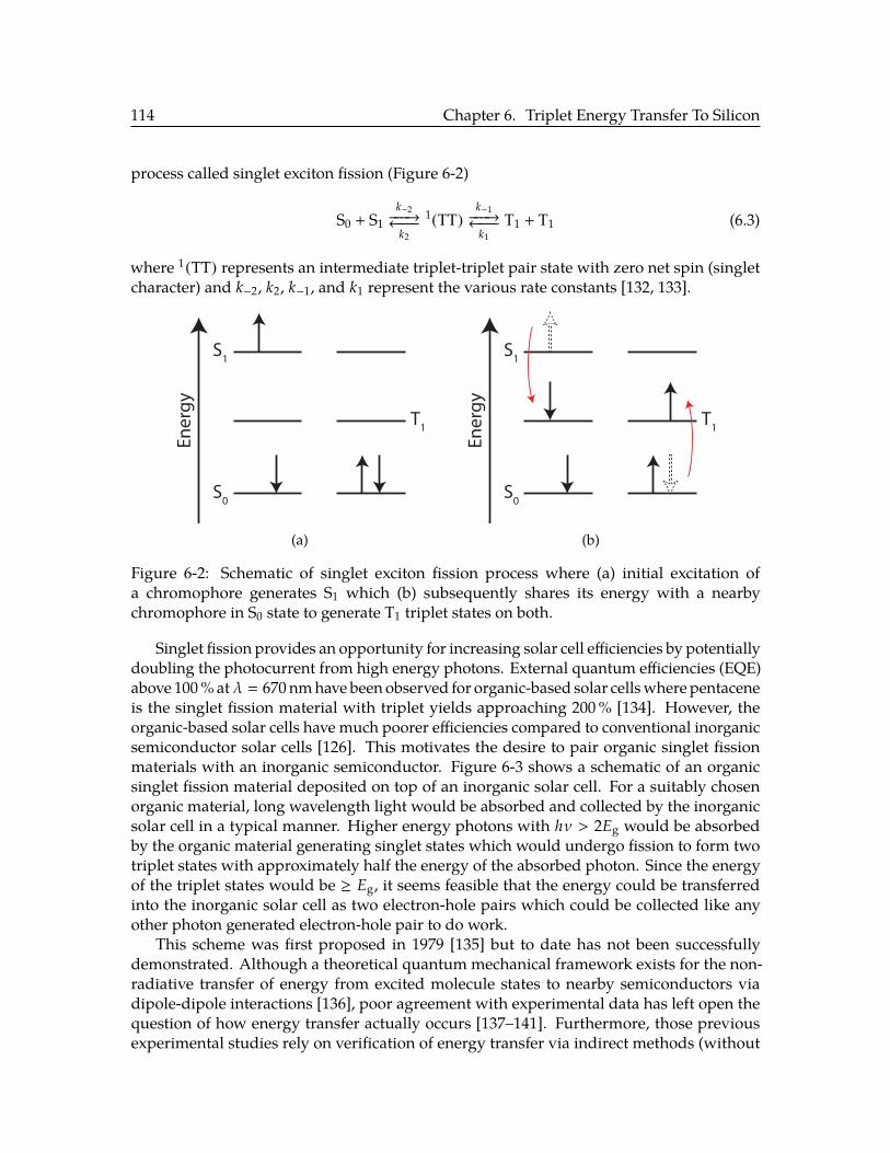
114 Chapter 6. Triplet Energy Transfer To Silicon
process called singlet exciton fission (Figure 6-2)
S0 + S1
k−2
−−−→←−−−
k2
1(TT)k−1
−−−→←−−−
k1
T1 + T1 (6.3)
where1(TT) represents an intermediate triplet-triplet pair state with zero net spin (singlet
character) and k−2, k2, k−1, and k1 represent the various rate constants [132, 133].
S0
S1
T1
Ener
gy
(a)
S0
S1
T1
Ener
gy
(b)
Figure 6-2: Schematic of singlet exciton fission process where (a) initial excitation of
a chromophore generates S1 which (b) subsequently shares its energy with a nearby
chromophore in S0 state to generate T1 triplet states on both.
Singlet fission provides an opportunity for increasing solar cell efficiencies by potentially
doubling the photocurrent from high energy photons. External quantum efficiencies (EQE)
above 100 % at λ 670 nm have been observed for organic-based solar cells where pentacene
is the singlet fission material with triplet yields approaching 200 % [134]. However, the
organic-based solar cells have much poorer efficiencies compared to conventional inorganic
semiconductor solar cells [126]. This motivates the desire to pair organic singlet fission
materials with an inorganic semiconductor. Figure 6-3 shows a schematic of an organic
singlet fission material deposited on top of an inorganic solar cell. For a suitably chosen
organic material, long wavelength light would be absorbed and collected by the inorganic
solar cell in a typical manner. Higher energy photons with hν > 2Eg would be absorbed
by the organic material generating singlet states which would undergo fission to form two
triplet states with approximately half the energy of the absorbed photon. Since the energy
of the triplet states would be ≥ Eg, it seems feasible that the energy could be transferred
into the inorganic solar cell as two electron-hole pairs which could be collected like any
other photon generated electron-hole pair to do work.
This scheme was first proposed in 1979 [135] but to date has not been successfully
demonstrated. Although a theoretical quantum mechanical framework exists for the non-
radiative transfer of energy from excited molecule states to nearby semiconductors via
dipole-dipole interactions [136], poor agreement with experimental data has left open the
question of how energy transfer actually occurs [137–141]. Furthermore, those previous
experimental studies rely on verification of energy transfer via indirect methods (without
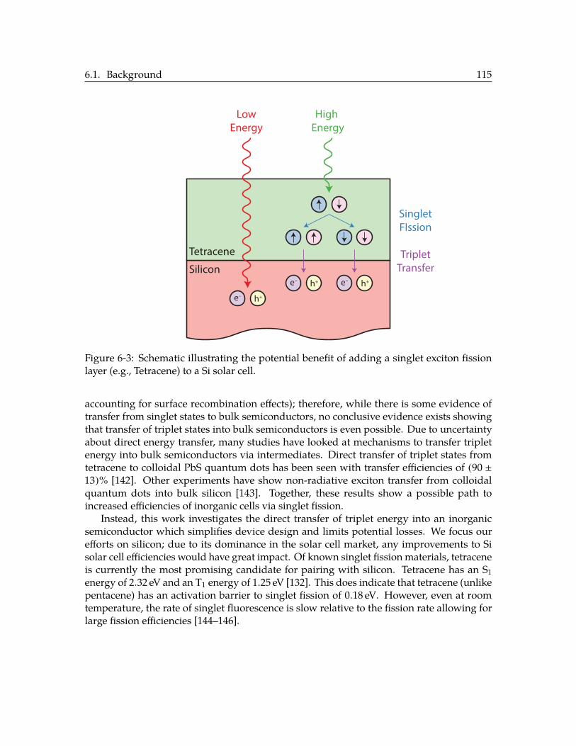
6.1. Background 115
Tetracene
Silicon
LowEnergy
High Energy
SingletFIssion
TripletTransfer
Figure 6-3: Schematic illustrating the potential benefit of adding a singlet exciton fission
layer (e.g., Tetracene) to a Si solar cell.
accounting for surface recombination effects); therefore, while there is some evidence of
transfer from singlet states to bulk semiconductors, no conclusive evidence exists showing
that transfer of triplet states into bulk semiconductors is even possible. Due to uncertainty
about direct energy transfer, many studies have looked at mechanisms to transfer triplet
energy into bulk semiconductors via intermediates. Direct transfer of triplet states from
tetracene to colloidal PbS quantum dots has been seen with transfer efficiencies of (90 ±
13)% [142]. Other experiments have show non-radiative exciton transfer from colloidal
quantum dots into bulk silicon [143]. Together, these results show a possible path to
increased efficiencies of inorganic cells via singlet fission.
Instead, this work investigates the direct transfer of triplet energy into an inorganic
semiconductor which simplifies device design and limits potential losses. We focus our
efforts on silicon; due to its dominance in the solar cell market, any improvements to Si
solar cell efficiencies would have great impact. Of known singlet fission materials, tetracene
is currently the most promising candidate for pairing with silicon. Tetracene has an S1
energy of 2.32 eV and an T1 energy of 1.25 eV [132]. This does indicate that tetracene (unlike
pentacene) has an activation barrier to singlet fission of 0.18 eV. However, even at room
temperature, the rate of singlet fluorescence is slow relative to the fission rate allowing for
large fission efficiencies [144–146].
116 Chapter 6. Triplet Energy Transfer To Silicon
6.2 Modeling SRV RequirementsWhile the exact mechanism for energy transfer is unknown, it is reasonable to expect that
energy from photons absorbed by tetracene and transferred into Si likely generates carriers
located closer to the Si surface than if tetracene was absent and the photon had been
absorbed directly by Si. Non-radiative energy transfer of excited states within molecules are
primarily thought to occur by either (1) dipole-dipole coupling interactions also known as
Förster resonance energy transfer (FRET) or (2) electron exchange via wavefunction overlap
also known as Dexter energy transfer [147, 148]. FRET rate constants are proportional
to 1/R6where R is the separation distance. This leads to relatively efficient transfer over
distances up to 100 Å in many molecular systems. However, triplet-triplet transfers are
spin forbidden from FRET leading to the (speculative) assumption that transfer of triplets
from tetracene to silicon will occur through a Dexter-like process. Because Dexter transfer
requires wavefunction overlap, the transfer rate exponentially decays with separation
distance and typically requires much shorter separations than for FRET. It should also be
noted that at present, it is unclear what physically acts as the acceptor state in Si.
Because the surface acts as a recombination center, it is worth determining what surface
conditions are required to see benefits from the addition of tetracene to a Si solar cell. In
this section, we model what surface recombination velocity (SRV) is required for transfer to
be useful assuming that transfer of energy from tetracene to silicon generates two electron
hole pairs per incident photon (of sufficient energy) but places those carriers close to a
surface which increases carrier recombination.
Solar cell simulations were made using PC1D1 which solves the two-carrier semiclassical
semiconductor transport equations coupled with Poisson’s equation using a finite-element
method. Figure 6-4 shows a representative plot of internal quantum efficiency (IQE) vs
wavelength for Si solar cells with varying front SRV. The IQE is defined as
IQE # of collected carriers
# of absorbed photons
(6.4)
and thus represents the fraction of generated carriers which are collected before recombi-
nation (minority carriers successfully diffuse to the junction). The IQE is maximum for
wavelengths where carriers are primarily generated within a diffusion length of the junction
(∼900 nm). The decrease in IQE for shorter wavelengths results from the fact that high
energy photons are absorbed closer to the surface and are therefore more influenced by the
front surface recombination velocity. Similarly, the drop in IQE for longer wavelengths is
related to the fact that carriers are generated throughout the wafer and longer diffusion
distances are required for collection (bulk and rear surface recombination can reduce the
number of collected carriers).
We assume that a benefit is received from addition of tetracene due to generation of
triplet pairs from singlet fission if the IQE for carriers generated within∼10 nm of the surface
1PC1Dmod6.2 and PC1D for Matlab are available at https://www2.pvlighthouse.com.au/resources/PC1D/
PC1Dmod6/PC1Dmod6.aspx
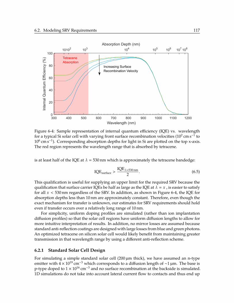
6.2. Modeling SRV Requirements 117
Wavelength (nm)300 400 500 600 700 800 900 1000 1100 1200
Inte
rnal
Qua
ntu
m E
ffici
ency
(%
)
0
20
40
60
80
100
Absorption Depth (nm)
10102 103 104 105 106 107 108
Increasing SurfaceRecombination Velocity
TetraceneAbsorption
Figure 6-4: Sample representation of internal quantum efficiency (IQE) vs. wavelength
for a typical Si solar cell with varying front surface recombination velocities (102
cm s−1
to
106
cm s−1
). Corresponding absorption depths for light in Si are plotted on the top x-axis.
The red region represents the wavelength range that is absorbed by tetracene.
is at least half of the IQE at λ 530 nm which is approximately the tetracene bandedge:
IQEsurface
>IQEλ530 nm
2
. (6.5)
This qualification is useful for supplying an upper limit for the required SRV because the
qualification that surface carrier IQEs be half as large as the IQE at λ x , is easier to satisfy
for all x < 530 nm regardless of the SRV. In addition, as shown in Figure 6-4, the IQE for
absorption depths less than 10 nm are approximately constant. Therefore, even though the
exact mechanism for transfer is unknown, our estimates for SRV requirements should hold
even if transfer occurs over a relatively long range of 10 nm.
For simplicity, uniform doping profiles are simulated (rather than ion implantation
diffusion profiles) so that the solar cell regions have uniform diffusion lengths to allow for
more intuitive interpretation of results. In addition, no mirror losses are assumed because
standard anti-reflection coatings are designed with large losses from blue and green photons.
An optimized tetracene on silicon solar cell would likely benefit from maintaining greater
transmission in that wavelength range by using a different anti-reflection scheme.
6.2.1 Standard Solar Cell Design
For simulating a simple standard solar cell (200 µm thick), we have assumed an n-type
emitter with 4 × 10¹⁹
cm−3
which corresponds to a diffusion length of ∼1 µm. The base is
p-type doped to 1 × 10¹⁶
cm−3
and no surface recombination at the backside is simulated.
1D simulations do not take into account lateral current flow to contacts and thus end up
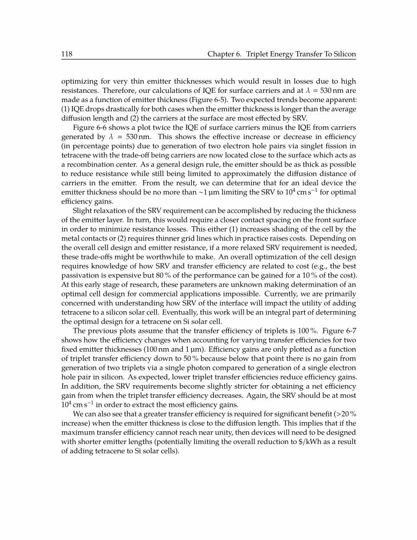
118 Chapter 6. Triplet Energy Transfer To Silicon
optimizing for very thin emitter thicknesses which would result in losses due to high
resistances. Therefore, our calculations of IQE for surface carriers and at λ 530 nm are
made as a function of emitter thickness (Figure 6-5). Two expected trends become apparent:
(1) IQE drops drastically for both cases when the emitter thickness is longer than the average
diffusion length and (2) the carriers at the surface are most effected by SRV.
Figure 6-6 shows a plot twice the IQE of surface carriers minus the IQE from carriers
generated by λ 530 nm. This shows the effective increase or decrease in efficiency
(in percentage points) due to generation of two electron hole pairs via singlet fission in
tetracene with the trade-off being carriers are now located close to the surface which acts as
a recombination center. As a general design rule, the emitter should be as thick as possible
to reduce resistance while still being limited to approximately the diffusion distance of
carriers in the emitter. From the result, we can determine that for an ideal device the
emitter thickness should be no more than ∼1 µm limiting the SRV to 104
cm s−1
for optimal
efficiency gains.
Slight relaxation of the SRV requirement can be accomplished by reducing the thickness
of the emitter layer. In turn, this would require a closer contact spacing on the front surface
in order to minimize resistance losses. This either (1) increases shading of the cell by the
metal contacts or (2) requires thinner grid lines which in practice raises costs. Depending on
the overall cell design and emitter resistance, if a more relaxed SRV requirement is needed,
these trade-offs might be worthwhile to make. An overall optimization of the cell design
requires knowledge of how SRV and transfer efficiency are related to cost (e.g., the best
passivation is expensive but 80 % of the performance can be gained for a 10 % of the cost).
At this early stage of research, these parameters are unknown making determination of an
optimal cell design for commercial applications impossible. Currently, we are primarily
concerned with understanding how SRV of the interface will impact the utility of adding
tetracene to a silicon solar cell. Eventually, this work will be an integral part of determining
the optimal design for a tetracene on Si solar cell.
The previous plots assume that the transfer efficiency of triplets is 100 %. Figure 6-7
shows how the efficiency changes when accounting for varying transfer efficiencies for two
fixed emitter thicknesses (100 nm and 1 µm). Efficiency gains are only plotted as a function
of triplet transfer efficiency down to 50 % because below that point there is no gain from
generation of two triplets via a single photon compared to generation of a single electron
hole pair in silicon. As expected, lower triplet transfer efficiencies reduce efficiency gains.
In addition, the SRV requirements become slightly stricter for obtaining a net efficiency
gain from when the triplet transfer efficiency decreases. Again, the SRV should be at most
104
cm s−1
in order to extract the most efficiency gains.
We can also see that a greater transfer efficiency is required for significant benefit (>20 %
increase) when the emitter thickness is close to the diffusion length. This implies that if the
maximum transfer efficiency cannot reach near unity, then devices will need to be designed
with shorter emitter lengths (potentially limiting the overall reduction to $/kWh as a result
of adding tetracene to Si solar cells).

6.2. Modeling SRV Requirements 119
(a)
SRV (cm/s)
102
103
104
105
106
Em
itte
r T
hic
kness (µ
m)
0.1
1
10
0
20
40
60
80
100
(b)
SRV (cm/s)
102
103
104
105
106
Em
itte
r T
hic
kness (µ
m)
0.1
1
10
0
20
40
60
80
100
Figure 6-5: IQE for (a) surface carriers and (b) λ 530 nm for varying emitter thicknesses
and front surface SRV for a conventional Si solar cell design.
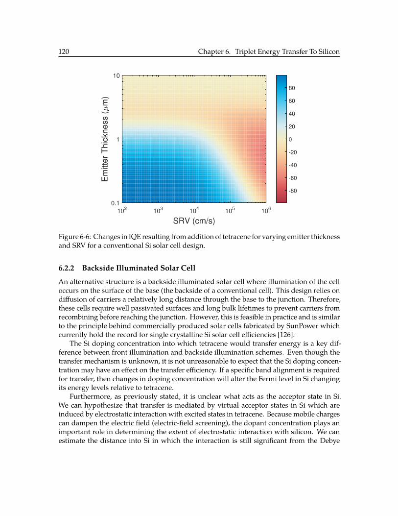
120 Chapter 6. Triplet Energy Transfer To Silicon
SRV (cm/s)
102
103
104
105
106
Em
itte
r T
hic
kness (µ
m)
0.1
1
10
-80
-60
-40
-20
0
20
40
60
80
Figure 6-6: Changes in IQE resulting from addition of tetracene for varying emitter thickness
and SRV for a conventional Si solar cell design.
6.2.2 Backside Illuminated Solar Cell
An alternative structure is a backside illuminated solar cell where illumination of the cell
occurs on the surface of the base (the backside of a conventional cell). This design relies on
diffusion of carriers a relatively long distance through the base to the junction. Therefore,
these cells require well passivated surfaces and long bulk lifetimes to prevent carriers from
recombining before reaching the junction. However, this is feasible in practice and is similar
to the principle behind commercially produced solar cells fabricated by SunPower which
currently hold the record for single crystalline Si solar cell efficiencies [126].
The Si doping concentration into which tetracene would transfer energy is a key dif-
ference between front illumination and backside illumination schemes. Even though the
transfer mechanism is unknown, it is not unreasonable to expect that the Si doping concen-
tration may have an effect on the transfer efficiency. If a specific band alignment is required
for transfer, then changes in doping concentration will alter the Fermi level in Si changing
its energy levels relative to tetracene.
Furthermore, as previously stated, it is unclear what acts as the acceptor state in Si.
We can hypothesize that transfer is mediated by virtual acceptor states in Si which are
induced by electrostatic interaction with excited states in tetracene. Because mobile charges
can dampen the electric field (electric-field screening), the dopant concentration plays an
important role in determining the extent of electrostatic interaction with silicon. We can
estimate the distance into Si in which the interaction is still significant from the Debye
6.2. Modeling SRV Requirements 121
(a)
102
103
104
105
106
SRV (cm/s)
50
60
70
80
90
100T
riple
t T
ransfe
r E
ffic
iency (
%)
-80
-60
-40
-20
0
20
40
60
80
(b)
102
103
104
105
106
SRV (cm/s)
50
60
70
80
90
100
Triple
t T
ransfe
r E
ffic
iency (
%)
-80
-60
-40
-20
0
20
40
60
80
Figure 6-7: Changes in IQE for (a) 100 nm and (b) 1 µm emitter thickness for varying triplet
transfer efficiencies and SRV for a conventional Si solar cell design.
122 Chapter 6. Triplet Energy Transfer To Silicon
length, LD:
LD
√εkBTq2ND
(6.6)
where ND is the dopant concentration. At room temperature in Si, the Debye length
varies from ∼130 nm when ND 1015
cm−3
to ∼1 nm when ND 1019
cm−3
. Therefore,
lower doping concentrations may improve transfer efficiencies. Because the emitter requires
relatively high doping concentrations, this would favor combining tetracene with a backside
illuminated solar cell.
Similar simulations as the previous section were run but the emitter thickness is now
fixed. The emitter thickness only needs to be optimized for resistance rather than diffusion
lengths. Furthermore, lateral conduction is no longer an issue as shading of the backside
is not a concern. IQE simulations were instead run as a function of both SRV and bulk
lifetimes which are more important now that the carriers have to diffuse a relatively large
distance in order to be collected (Figure 6-8). Compared to a conventional solar cell, the
absolute IQE is more sensitive to SRV in a backside illuminated solar cell. This holds true
for both surface carriers and those generated by 530 nm light, even when the bulk lifetime
is relatively long.
Similar to before, we can generate a plot of twice the IQE of surface carriers minus
the IQE from carriers generated by λ 530 nm (Figure 6-9). For this design, efficiency is
never lost by the addition of tetracene. However, for long bulk lifetimes, there is a drastic
decrease in the efficiency gain from ∼100 % near S 102
cm s−1
to ∼0 % near S 104
cm s−1
.
Therefore, even though the presence of tetracene will not decrease the efficiency, the SRV
needs to be below 104
cm s−1
for any practical efficiency gains. Figure 6-10 shows how the
efficiency changes when accounting for varying transfer efficiencies assuming a bulk lifetime
of 1000 µs. Compared to the conventional cells, the SRV requirements for efficiency gains
increase more sharply as transfer efficiency decreases. In addition, the transfer efficiency
needs to exceed ∼60 % for any significant gains.
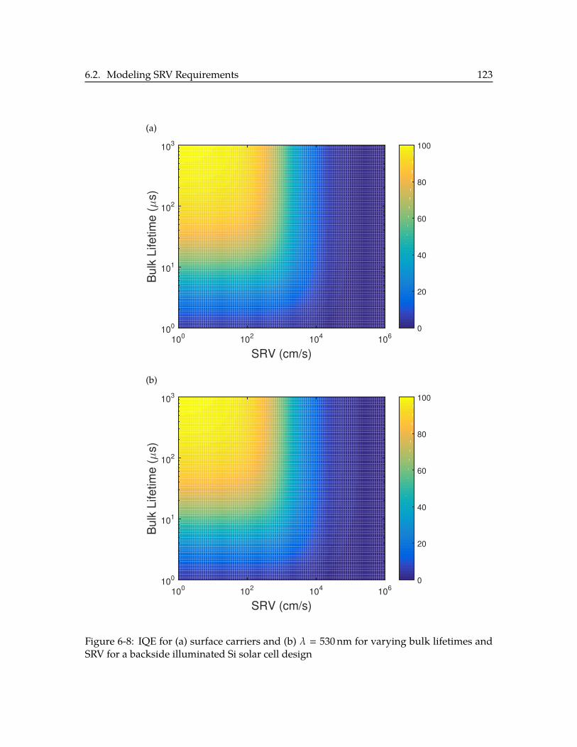
6.2. Modeling SRV Requirements 123
(a)
SRV (cm/s)
100
102
104
106
Bu
lk L
ife
tim
e (µ
s)
100
101
102
103
0
20
40
60
80
100
(b)
SRV (cm/s)
100
102
104
106
Bu
lk L
ife
tim
e (µ
s)
100
101
102
103
0
20
40
60
80
100
Figure 6-8: IQE for (a) surface carriers and (b) λ 530 nm for varying bulk lifetimes and
SRV for a backside illuminated Si solar cell design
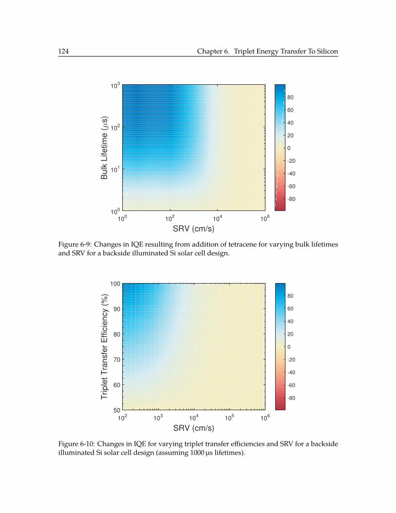
124 Chapter 6. Triplet Energy Transfer To Silicon
SRV (cm/s)
100
102
104
106
Bulk
Lifetim
e (µ
s)
100
101
102
103
-80
-60
-40
-20
0
20
40
60
80
Figure 6-9: Changes in IQE resulting from addition of tetracene for varying bulk lifetimes
and SRV for a backside illuminated Si solar cell design.
102
103
104
105
106
SRV (cm/s)
50
60
70
80
90
100
Triple
t T
ransfe
r E
ffic
iency (
%)
-80
-60
-40
-20
0
20
40
60
80
Figure 6-10: Changes in IQE for varying triplet transfer efficiencies and SRV for a backside
illuminated Si solar cell design (assuming 1000 µs lifetimes).

6.3. Radio Frequency Photoconductivity Decay (RFPCD) 125
6.3 Radio Frequency Photoconductivity Decay (RFPCD)For either proposed solar cell structure, the quality of the interface between tetracene and
silicon is of great importance requiring that the interface be well passivated. Transient
radio frequency photoconductivity decay (RFPCD) measurements which are typically used
to measure minority carrier recombination lifetimes can provide a quick and contactless
method to determine the quality of the silicon surface. The basic operating principle of
RFPCD was first developed by Miller in 1976 [149]. A schematic of our RFPCD experimental
apparatus is shown in Figure 6-11. The conductance of a wafer is inductively measured
through the use of an RF coil which acts as the primary of a transformer while the wafer
being measured acts as a short-circuited secondary. A pulsed LED light source is used to
optically generate excess carriers increasing the conductivity of the material.
Figure 6-11: Schematic of RFPCD experimental apparatus.
Because generation and recombination processes balance (Section 2.1), the change in
excess carrier concentration (which is proportional to the measured signal) with time can
be calculated from
d∆ndt
G −U Gexternal −∆nτ
(6.7)
where Gexternal is the generation rate due to some external source which is the LED light
source. If our illumination is kept constant during excitation (Gexternal g) then
∆n gτ(1 − e
−t/τ). (6.8)
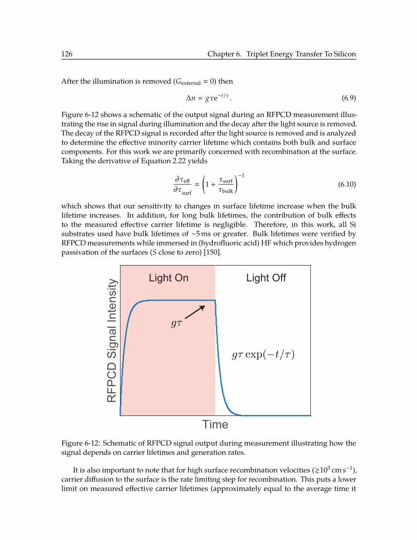
126 Chapter 6. Triplet Energy Transfer To Silicon
After the illumination is removed (Gexternal 0) then
∆n gτe−t/τ . (6.9)
Figure 6-12 shows a schematic of the output signal during an RFPCD measurement illus-
trating the rise in signal during illumination and the decay after the light source is removed.
The decay of the RFPCD signal is recorded after the light source is removed and is analyzed
to determine the effective minority carrier lifetime which contains both bulk and surface
components. For this work we are primarily concerned with recombination at the surface.
Taking the derivative of Equation 2.22 yields
∂τeff
∂τsurf
(1 +
τsurf
τbulk
)−1
(6.10)
which shows that our sensitivity to changes in surface lifetime increase when the bulk
lifetime increases. In addition, for long bulk lifetimes, the contribution of bulk effects
to the measured effective carrier lifetime is negligible. Therefore, in this work, all Si
substrates used have bulk lifetimes of ∼5 ms or greater. Bulk lifetimes were verified by
RFPCD measurements while immersed in (hydrofluoric acid) HF which provides hydrogen
passivation of the surfaces (S close to zero) [150].
gτ
gτ exp(−t/τ)
Time
RFP
CD
Sig
nal I
nten
sity Light OffLight On
Figure 6-12: Schematic of RFPCD signal output during measurement illustrating how the
signal depends on carrier lifetimes and generation rates.
It is also important to note that for high surface recombination velocities (&103
cm s−1
),
carrier diffusion to the surface is the rate limiting step for recombination. This puts a lower
limit on measured effective carrier lifetimes (approximately equal to the average time it
6.3. Radio Frequency Photoconductivity Decay (RFPCD) 127
takes a carrier to diffuse to the surface) of
τeff d2
Dπ2
(6.11)
where d is the wafer thickness and D is the diffusivity of the minority carrier. For the
wafers employed in this work, this corresponds to about 38 µs (6-inch, 5 × 10¹¹
cm−3
doping
n-type) and 44 µs (8-inch, 5 × 10¹⁴
cm−3
doping n-type). For low surface recombination
velocities < d/τbulk, the effective carrier lifetime is essentially a measure of the bulk lifetime.
In the intermediate range, the surface recombination velocity can be approximated from
the effective lifetime by the following expression:
τeff d
2S. (6.12)
6.3.1 Determination of Transfer Yields via RFPCD
Another important feature of Figure 6-12, is that when the pulse duration is much larger than
the effective lifetime (tpulse τ), the signal saturates during illumination at a value equal to
gτ. Therefore, by employing long pulses we can extract information about the generation
rate of carriers in the silicon once τ is extracted from the decay transient. Obtaining absolute
measurements of the generation rate using this method are difficult in practice due to the
need for calibration measurements and careful control of experimental parameters (e.g.,
illumination intensity, distribution, and position relative to sample and coil). Therefore, gτextracted from RFPCD is typically ignored. However, comparison of similar samples under
controlled conditions can yield useful information about relative changes in generation rate.
Figure 6-13 shows a schematic of how comparison of RFPCD measurements can be used to
determine if energy is transferred from tetracene to silicon. First measurements are made
using a sample without tetracene to establish a baseline generation rate. Then a sample
tetracene deposited onto a similar sample is measured and the obtained generation rates
are compared. When the illumination wavelength is greater than the tetracene absorption
band edge, if no energy transfer is occuring, then the signal should decrease based on the
amount of the light absorbed by tetracene which can be estimated from the Beer-Lamber
law
1 −I(d)
I0
1 − exp(−αd) (6.13)
where 1 − I(d)/I0 is the fraction of absorbed light, d is the thickness of tetracene, and α is
the absorption coefficient of tetracene which can be related to the imaginary component of
the refractive index, κ, by
α 4πκλ
(6.14)
where λ is the wavelength of light. If the ratio of the generation rate without tetracene to
with tetracene exceeds the fraction of absorbed light, then some of the energy absorbed by
the tetracene is being transferred to silicon. This alone, however, does not indicate whether
transfer involves any triplet states generated via singlet fission. Excited singlet states can
transfer into silicon as well as fluoresce leading to absorption of some fraction of fluoresced
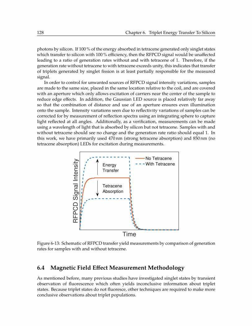
128 Chapter 6. Triplet Energy Transfer To Silicon
photons by silicon. If 100 % of the energy absorbed in tetracene generated only singlet states
which transfer to silicon with 100 % efficiency, then the RFPCD signal would be unaffected
leading to a ratio of generation rates without and with tetracene of 1. Therefore, if the
generation rate without tetracene to with tetracene exceeds unity, this indicates that transfer
of triplets generated by singlet fission is at least partially responsible for the measured
signal.
In order to control for unwanted sources of RFPCD signal intensity variations, samples
are made to the same size, placed in the same location relative to the coil, and are covered
with an aperture which only allows excitation of carriers near the center of the sample to
reduce edge effects. In addition, the Gaussian LED source is placed relatively far away
so that the combination of distance and use of an aperture ensures even illumination
onto the sample. Intensity variations seen due to reflectivity variations of samples can be
corrected for by measurement of reflection spectra using an integrating sphere to capture
light reflected at all angles. Additionally, as a verification, measurements can be made
using a wavelength of light that is absorbed by silicon but not tetracene. Samples with and
without tetracene should see no change and the generation rate ratio should equal 1. In
this work, we have primarily used 470 nm (strong tetracene absorption) and 850 nm (no
tetracene absorption) LEDs for excitation during measurements.
Time
RF
PC
D S
ignal In
tensity No Tetracene
With TetraceneEnergy
Transfer
Tetracene
Absorption
Figure 6-13: Schematic of RFPCD transfer yield measurements by comparison of generation
rates for samples with and without tetracene.
6.4 Magnetic Field Effect Measurement MethodologyAs mentioned before, many previous studies have investigated singlet states by transient
observation of fluorescence which often yields inconclusive information about triplet
states. Because triplet states do not fluoresce, other techniques are required to make more
conclusive observations about triplet populations.

6.4. Magnetic Field Effect Measurement Methodology 129
One such technique applicable to both photoluminescence and photocurrent measur-
ments is to observed changes in signal intensity as a function of applied magnetic field.
Singlet fission rates are dependent on external magnetic fields as explained by the Mer-
rifield model [151, 152]. As shown in Equation 6.3, during singlet fission, intermediate
triplet-triplet pair states form. For spin conservation to hold, the pair state must have singlet
character. Looking at all the possible spin combinations for a triplet-triplet pair, at zero
magnetic field there are three possible triplet-triplet pairs with singlet character. For small
applied magnetic fields, the number of singlet character pairs increases. For large applied
magnetic fields, the number of singlet character pairs decreases to 2. The fission rate, kfis,
depends on the number of possible singlet character states, N , in the following way
kfis ∝N
k2/k−1 + N(6.15)
which means that the singlet fission rate can be reduced by application of a magnetic
field. Therefore, when we are monitoring a process in which there is competition between
singlet and triplet states, changes in the signal can indicate contributions from triplet states
as seen in Figure 6-14 for fluorescence and photocurrent from a tetracene based organic
solar cell. Under applied magnetic as the singlet fission rate decreases, competition to
singlet fluorescence from singlet fission is reduced leading to increased singlet fluorescence
signal. Conversely, photocurrent measurements of the same device show a decrease with
magnetic field indicating that non-emissive triplet states are contributing to the observed
photocurrent signal.
0 0.1 0.2 0.3 0.4 0.5
Magnetic Field (T)
-1.5
-1
-0.5
0
0.5
1
1.5
Ph
oto
cu
rre
nt
Ch
an
ge
(%
)
-15
-10
-5
0
5
10
15
Flu
ore
scence C
hange (
%)
Figure 6-14: Example of using magnetic field effect measurements to identify triplet
contributions to signal as seen for fluorescence and photocurrent from tetracene based
organic solar cells. Reproduced from [146]
In addition to analysis of generation rate ratios via RFPCD, we propose using measure-
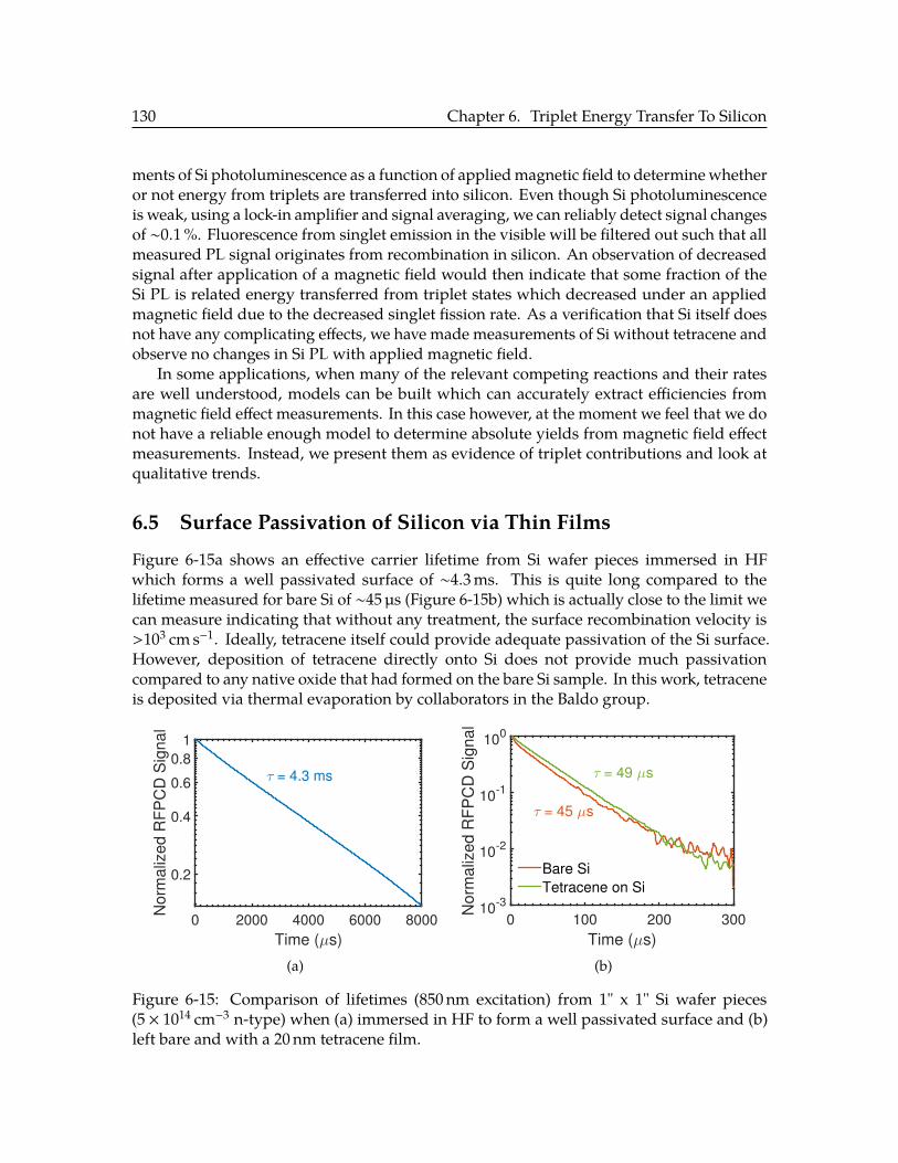
130 Chapter 6. Triplet Energy Transfer To Silicon
ments of Si photoluminescence as a function of applied magnetic field to determine whether
or not energy from triplets are transferred into silicon. Even though Si photoluminescence
is weak, using a lock-in amplifier and signal averaging, we can reliably detect signal changes
of ∼0.1 %. Fluorescence from singlet emission in the visible will be filtered out such that all
measured PL signal originates from recombination in silicon. An observation of decreased
signal after application of a magnetic field would then indicate that some fraction of the
Si PL is related energy transferred from triplet states which decreased under an applied
magnetic field due to the decreased singlet fission rate. As a verification that Si itself does
not have any complicating effects, we have made measurements of Si without tetracene and
observe no changes in Si PL with applied magnetic field.
In some applications, when many of the relevant competing reactions and their rates
are well understood, models can be built which can accurately extract efficiencies from
magnetic field effect measurements. In this case however, at the moment we feel that we do
not have a reliable enough model to determine absolute yields from magnetic field effect
measurements. Instead, we present them as evidence of triplet contributions and look at
qualitative trends.
6.5 Surface Passivation of Silicon via Thin FilmsFigure 6-15a shows an effective carrier lifetime from Si wafer pieces immersed in HF
which forms a well passivated surface of ∼4.3 ms. This is quite long compared to the
lifetime measured for bare Si of ∼45 µs (Figure 6-15b) which is actually close to the limit we
can measure indicating that without any treatment, the surface recombination velocity is
>103
cm s−1
. Ideally, tetracene itself could provide adequate passivation of the Si surface.
However, deposition of tetracene directly onto Si does not provide much passivation
compared to any native oxide that had formed on the bare Si sample. In this work, tetracene
is deposited via thermal evaporation by collaborators in the Baldo group.
Time (µs)
0 2000 4000 6000 8000
No
rma
lize
d R
FP
CD
Sig
na
l
0.2
0.4
0.6
0.8
1
τ = 4.3 ms
(a)
Time (µs)
0 100 200 300
No
rma
lize
d R
FP
CD
Sig
na
l
10-3
10-2
10-1
100
Bare Si
Tetracene on Si
τ = 45 µs
τ = 49 µs
(b)
Figure 6-15: Comparison of lifetimes (850 nm excitation) from 1" x 1" Si wafer pieces
(5 × 10¹⁴
cm−3
n-type) when (a) immersed in HF to form a well passivated surface and (b)
left bare and with a 20 nm tetracene film.
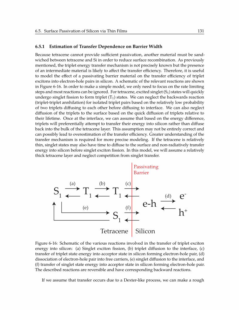
6.5. Surface Passivation of Silicon via Thin Films 131
6.5.1 Estimation of Transfer Dependence on Barrier Width
Because tetracene cannot provide sufficient passivation, another material must be sand-
wiched between tetracene and Si in order to reduce surface recombination. As previously
mentioned, the triplet energy transfer mechanism is not precisely known but the presence
of an intermediate material is likely to affect the transfer efficiency. Therefore, it is useful
to model the effect of a passivating barrier material on the transfer efficiency of triplet
excitons into electron-hole pairs in silicon. A schematic of the relevant reactions are shown
in Figure 6-16. In order to make a simple model, we only need to focus on the rate limiting
steps and most reactions can be ignored. For tetracene, excited singlet (S1) states will quickly
undergo singlet fission to form triplet (T1) states. We can neglect the backwards reaction
(triplet-triplet annhilation) for isolated triplet pairs based on the relatively low probability
of two triplets diffusing to each other before diffusing to interface. We can also neglect
diffusion of the triplets to the surface based on the quick diffusion of triplets relative to
their lifetime. Once at the interface, we can assume that based on the energy difference,
triplets will preferentially attempt to transfer their energy into silicon rather than diffuse
back into the bulk of the tetracene layer. This assumption may not be entirely correct and
can possibly lead to overestimation of the transfer efficiency. Greater understanding of the
transfer mechanism is required for more precise modeling. If the tetracene is relatively
thin, singlet states may also have time to diffuse to the surface and non-radiatively transfer
energy into silicon before singlet exciton fission. In this model, we will assume a relatively
thick tetracene layer and neglect competition from singlet transfer.
Tetracene Silicon
(a) (b) (c)
(d)
(e) (f)
PassivatingBarrier
Figure 6-16: Schematic of the various reactions involved in the transfer of triplet exciton
energy into silicon: (a) Singlet exciton fission, (b) triplet diffusion to the interface, (c)
transfer of triplet state energy into acceptor state in silicon forming electron-hole pair, (d)
dissociation of electron-hole pair into free carriers, (e) singlet diffusion to the interface, and
(f) transfer of singlet state energy into acceptor state in silicon forming electron-hole pair.
The described reactions are reversible and have corresponding backward reactions.
If we assume that transfer occurs due to a Dexter-like process, we can make a rough

132 Chapter 6. Triplet Energy Transfer To Silicon
estimation of the transfer rate dependence on thickness by modeling triplet transfer from
tetracene to silicon as tunneling through a potential barrier due to wavefunction overlap.
For 1-D quantum mechanical tunneling through a finite barrier, the transmission rate when
E < V0 is
T
1 +
V2
0sinh
2(ka)4E(V0 − E)
−1
(6.16)
where
k
√2m(V0 − E)~2
(6.17)
where V0 is the barrier height, a is the barrier width, E is the particle energy, and m is
the mass of the particle. We estimate the energy of the tunneling particle as the energy
difference between tetracene triplet state and silicon bandgap (1.25 eV − 1.12 eV 0.13 eV)
and the barrier height to be the difference in electron affinities of Si and SiO2 (4.05 eV −
0.95 eV 3.1 eV). This estimation only considers transport of electrons and assumes no
band alignment effects therefore yielding only a rough approximation. However, this
calculation is useful for providing an indication of the separation distances required for
transfer. Figure 6-17 shows that the transmission rate drops off sharply within 20 Å.
The calculated transmission rate gives the probability that an incident energetic particle
can tunnel across a barrier. The actual triplet transfer rate (ktrans) is modified by the fact
that triplet states attempt to tunnel through the barrier multiple times:
ktrans Tνattempt (6.18)
where νattempt is the tunneling attempt frequency and can be estimated by the triplet hopping
rate in tetracene,∼1013
s−1
[153]. If there were no competing processes, even for slow transfer
rates, the triplets would always eventually transfer to silicon. However, due to competing
processes (e.g., intersystem crossing and phosphorescence, triplet-triplet annihilation) we
expect triplet states can decay before transfer. The triplet state lifetime (τtriplet) in tetracene
is relatively long compared to singlet states, and has been observed to be a long as ∼50 µs
for bulk single crystal tetracene. However, measurements of thermally evaporated thin
films of tetracene (similar to the material used in this work), show much shorter triplet
state lifetimes of ∼50 ns which is hypothesized to be related to increased recombination at
surfaces [145]. Assuming first order reactions, we can estimate the actual transfer yield of
triplets in tetracene from
Transfer Yield ktrans
ktrans + τ−1
triplet
(6.19)
which has been plotted a function of barrier width in Figure 6-18. While near unity transfer
can be expected for ultra thin barriers, the transfer efficiency begins to drastically decrease
once the barrier becomes thicker than ∼2 nm. Therefore, based on these calculations and
our models for SRV requirements, a challenge to obtaining practical efficiency gains from
adding tetracene to a Si solar cell will be to develop a method for adequately passivating
the Si surface using an ultra thin barrier.
It should be noted that we neglected backtransfer of energy from silicon into tetracene.
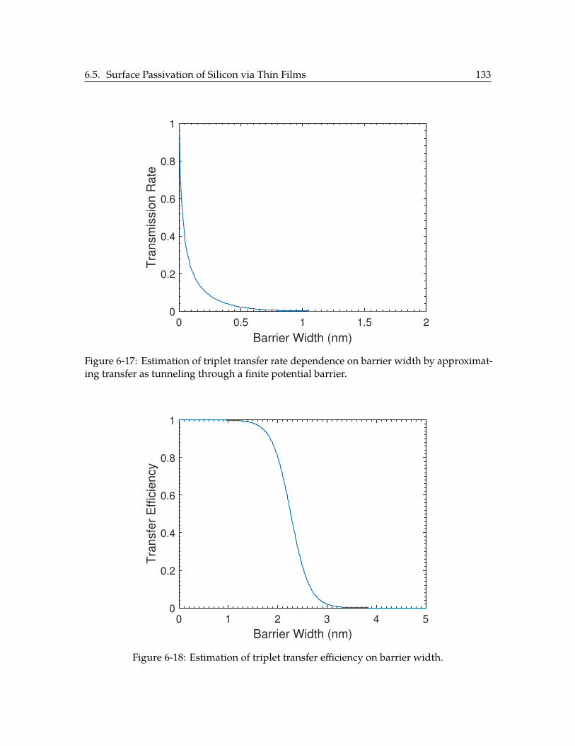
6.5. Surface Passivation of Silicon via Thin Films 133
Barrier Width (nm)
0 0.5 1 1.5 2
Tra
nsm
issio
n R
ate
0
0.2
0.4
0.6
0.8
1
Figure 6-17: Estimation of triplet transfer rate dependence on barrier width by approximat-
ing transfer as tunneling through a finite potential barrier.
0 1 2 3 4 5
Barrier Width (nm)
0
0.2
0.4
0.6
0.8
1
Tra
nsfe
r E
ffic
iency
Figure 6-18: Estimation of triplet transfer efficiency on barrier width.
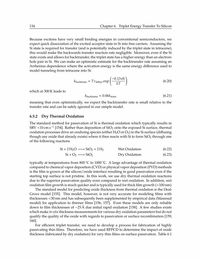
134 Chapter 6. Triplet Energy Transfer To Silicon
Because excitons have very small binding energies in conventional semiconductors, we
expect quick dissociation of the excited acceptor state in Si into free carriers. Assuming the
Si state is required for transfer (and is potentially induced by the triplet state in tetracene),
this would make the backwards transfer reaction rate negligible. Moreover, even if the Si
state exists and allows for backtransfer, the triplet state has a higher energy than an electron-
hole pair in Si. We can make an optimistic estimate for the backtransfer rate assuming an
Arrhenius dependence where the activation energy is the same energy difference used to
model tunneling from tetracene into Si:
kbacktrans Tνdebye exp
(−0.13 eV
kT
)(6.20)
which at 300 K leads to
kbacktrans ≈ 0.06ktrans (6.21)
meaning that even optimistically, we expect the backtransfer rate is small relative to the
transfer rate and can be safely ignored in our simple model.
6.5.2 Dry Thermal Oxidation
The standard method for passivation of Si is thermal oxidation which typically results in
SRV <10 cm s−1
[154]. Rather than deposition of SiO2 onto the exposed Si surface, thermal
oxidation processes drive an oxidizing species (either H2O or O2) to the Si surface (diffusing
though any oxide that already exists) where it then reacts with Si to form SiO2 through one
of the following reactions
Si + 2 H2O −−−→ SiO2 + 2 H2 Wet Oxidation (6.22)
Si + O2 −−−→ SiO2 Dry Oxidation (6.23)
typically at temperatures from 800C to 1000
C. A large advantage of thermal oxidation
compared to chemical vapor deposition (CVD) or physical vapor deposition (PVD) methods
is the film is grown at the silicon/oxide interface resulting in good passivation even if the
starting top surface is not pristine. In this work, we use dry thermal oxidation reactions
due to the superior passivation quality even compared to wet oxidation. In addition, wet
oxidation film growth is much quicker and is typically used for thick film growth (>100 nm).
The standard model for predicting oxide thickness from thermal oxidation is the Deal-
Grove model [155]. This model, however, is not very accurate for modeling films with
thicknesses <30 nm and has subsequently been supplemented by empirical data (Massoud
model) for application to thinner films [156, 157]. Even these models are only reliable
down to film thicknesses of ∼25 Å due initial rapid oxidation [158]. A few studies exists
which make in situ thickness measurements for various dry oxidation parameters but do not
qualify the quality of the oxide with regards to passivation or surface recombination [159,
160].
For efficient triplet transfer, we need to develop a process for fabrication of highly
passivating thin films. Therefore, we have used RFPCD to determine the impact of oxide
thickness (fabricated by dry oxidation) for very thin films on surface passivation. Table 6.1

6.5. Surface Passivation of Silicon via Thin Films 135
contains a summary results from dry oxidations including the growth parameters and
the resulting thicknesses as measured by spectroscopic ellipsometer. It should be noted
that spectroscopic ellipsometry is nominally accurate to ±2 Å but in practice accurate mea-
surement of very thin oxides is difficult as seen by studies comparing various thickness
measurement methodologies [161]. Also, the Si used in these experiments were high resis-
tivity (>10 000Ω cm) float zone wafers which showed some injection level dependence on
carrier lifetimes. Therefore, we only report approximate lifetimes which give an indication
of surface quality.
Oxide films down to 14 Å were successfully fabricated by dry oxidation showing the
potential for this technique to form thin barrier layers through which tunneling is possible.
However, with the current process, there is a clear trade-off in passivation quality as films
formed by short, low temperature growths have lifetimes almost two orders of magnitude
lower indicating significantly larger SRV.
Table 6.1: Summary of results from fabrication of thin oxide films via dry oxidation
Sample
Label
Temperature
(C)
O2 Flow
Duration
(min)
Thickness
(Å)
Effective
Carrier
Lifetime
(ms)
Surface
Preparationa
A 800 50 57 ∼5 SC2
B 800 10 33 ∼5 SC2
C 700 2 21 ∼5 SC2
D 700 2 19 ∼5 HF
E 700b
2 17 ∼0.05 to 0.1 SC2
F 700b
2 14 ∼0.05 to 0.1 HF
aWafers are RCA cleaned immediately before oxidation. This column signifies whether samples were given an
additional HF dip after SC2 to strip any oxide formed.
bThe furnace was cooled to 400
C before sample loading and then slowly ramped to the growth temperature.
6.5.3 Atomic Layer Deposition
Another method used in this work to fabricate thin oxide films was plasma-enhanced atomic
layer deposition (ALD). Deposition mechanism is similar to chemical vapor deposition but
the surface is exposed to separate precursors in repeated, sequential steps allowing for
layer-by-layer control of deposition giving precise control over the final film thickness. The
growth rate for SiO2 for the process used is ∼0.91 Å per cycle (as calibrated by measurement
of a 100 cycle film using spectroscopic ellipsometry). Films were fabricated using 5 cycles,
11 cycles, and 55 cycles with the expectation of yielding ∼5 Å, ∼10 Å, and ∼50 Å thick
films. Spectroscopy ellipsometry for 5 cycles and 11 cycles films yielded anomalously large
thicknesses making the real values uncertain. Therefore, the sample thicknesses for ALD
films will be reported based on the calibrated thickness per cycle. It is not unreasonable
that spectroscopic ellipsometry may give anomalous results due to the thickness being
extracted using complex refractive index data for thermal oxide films. Differences in film
136 Chapter 6. Triplet Energy Transfer To Silicon
densities between the two fabrication methods can lead to index of refraction variations
which may have resulted in the erroneous thickness values.
Our ALD process produces short lifetimes comparable to the thinnest dry oxide films of
approximately 40 µs to 120 µs. Representative RFPCD measurements from ALD deposition
of SiO2 are shown in Figure 6-19. A key difference between dry oxidation and ALD
deposition is that while ALD gives more control over deposition rate, the film is deposited
directly onto the surface of the sample. Because passivation quality largely depends on the
film immediately grown at the silicon interface, it is a challenge to prevent poor quality
native oxide formation before deposition via ALD. All of the samples pre-ALD are given
an additional HF dip step for 5 minutes after SC2 during RCA cleaning to strip any native
oxide and also leave the surface with hydrogen termination which should prevent native
oxidation for a short duration. Unfortunately, due to wafer rinsing and drying requirements
in the cleanroom facilities, the minimum time post HF dip to ALD chamber is ∼10 min. It
is possible that some native oxide forms in this time which results in the lower lifetimes
measured. However, ALD may still hold potential for forming well passivating thin films
based on the high quality passivation of Si via ALD that is common in industrial cleanroom
facilities.
Time (µs)0 50 100 150
Nor
mal
ized
RF
PC
D S
igna
l
0.2
0.4
0.6
0.8
1
5 Å: τ = 75 µs10 Å: τ = 91 µs50 Å: τ = 116 µs
Figure 6-19: Effective carrier lifetimes measured via RFPCD for films deposited by ALD for
varying film thicknesses.

6.6. Triplet Energy Transfer to Silicon 137
6.6 Triplet Energy Transfer to Silicon
6.6.1 Magnetic Field Effect (MFE) Photoluminescence
Thermally evaporated films of tetracene 20 nm thick were deposited on the various oxide
films fabricated in the previous section (Section 6.5). The methodology described in
Section 6.4 was then used to determine if any triplet states contribute to Si photoluminescence
and are therefore transferring their energy to Si. Control measurements of bare silicon
without tetracene do not show any dependence of PL on applied magnetic field. In addition,
measurements of samples with sufficiently thick oxides such that no non-radiative energy
transfer is expected (fabricated by both dry oxidation and ALD) show no evidence of
magnetic field dependent PL. Figure 6-20 shows a plot of the PL signal change percent as
a function of applied magnetic field for samples with tetracene on ALD deposited SiO2
films. The thickest film (50 Å) shows variations in the signal close to 0 % on the order of the
experimental noise indicating that no triplet transfer is occurring. However, there is a clear
decrease in PL from the thinner oxide films (5 Å and 10 Å) as magnetic field is decreasing.
The magnetic field is decreasing the singlet fission rate and thus altering the population
of triplet states in tetracene. Therefore, this decrease in PL signal shows the first clear
evidence that transfer of triplet state energy directly into silicon is possible. Furthermore,
our observations show a clear dependence of the signal change magnitude on the separation
distance (oxide thickness) as expected. Lack of observation of PL signal change from 50 Å
films is also consistent with our model (Section 6.5) which predicts that transfer is quickly
quenched by a couple nanometers of oxide.
Magnetic Field (T)0 0.1 0.2 0.3 0.4
PL
Sig
nal C
hang
e (%
)
-2.5
-2
-1.5
-1
-0.5
0
0.5
1
10 Å SiO2 (ALD)
50 Å SiO2 (ALD)
5 Å SiO2 (ALD)
Figure 6-20: Magnetic Field Effect (MFE) PL from ALD passivated samples showing transfer
of triplet energy into Si.

138 Chapter 6. Triplet Energy Transfer To Silicon
The signal in MFE PL measurements are obtained by filtering out visible light (to remove
signal from singlet fluorescence) and integration of the near-IR spectra to as collect as much
silicon emission as possible due it being an indirect material and thus a poor emitter. In
order to verify that the observed PL signal always originates in silicon and that MFE PL
is not a result of triplet phosphorescence (unlikely due to low probability), PL spectra
were obtained for samples with and without tetracene. Figure 6-21 shows that the spectra
are reasonably well matched indicating that our measurements are only probing silicon
emission and that the MFE changes observed are indeed due to transfer of triplet energy to
silicon.
Wavelength (nm)
900 1000 1100 1200 1300
Inte
nsity (
arb
. u
nits)
0
0.2
0.4
0.6
0.8
1
1.2
Bare Silicon
Tetracene Coated Si
Figure 6-21: Photoluminescence spectra comparison show that emission from tetracene
coated Si matches that of bare Si.
Similar MFE results are obtained from samples fabricated via dry oxidation. No MFE
was observed for samples with oxides thicker than 19 Å. Unfortunately, this means we have
yet to develop a film thin enough for transfer while maintaining the surface passivation
quality expected from dry oxidation. While we have shown evidence of transfer, further
improvement of the surface quality from very thin films will likely be required for useful
solar cell efficiency increases (discussed more in Section 6.2). The two thinner dry oxide
samples (E and F) showed weak MFE PL changes approximately an order of magnitude
lower percent change in signal compared to ALD samples. The decrease in signal is mostly
likely due to the slightly larger thicknesses of the dry oxide samples.
6.6.2 Changes in Generation Rate Measured by RFPCD
To verify the methodology described in Section 6.3.1, generation rates were measured via
RFPCD for samples with and without tetracene containing sufficiently thick (50 nm and

6.6. Triplet Energy Transfer to Silicon 139
100 nm) that no non-radiative energy transfer is expected from tetracene to silicon. Figure 6-
22 contains a plot of the generation rate ratios for samples with 20 nm thick tetracene films
to without tetracene under optical excitation at 850 nm and 470 nm. Because tetracene does
not absorb the excitation and should not affect the reflectivity much for a 20 nm film, under
850 nm excitation, the generation rate with and without tetracene should be identical and
the generation rate ratio should be equal to 1 as observed (with a few percent error). Under
470 nm excitation, the tetracene should absorb 14 % of the light in 20 nm based on an a
measured absorption coefficient of 7.5 × 10⁴
cm−1
assuming a single optical pass. Therefore
we expect the generation rate ratio to be ∼0.86 with tetracene if no transfer is occurring. We
also see this to within a few percent confirming that our measurements are consistent with
expectations when energy transfer is absent. The discrepancy may be related to scattering
of light by tetracene or changes to the effective path absorption path length in tetracene due
to destructive interference (created by reflections off the various interfaces present).
SiO2 Thickness (nm)
40 50 60 70 80 90 100 110
Genera
tion R
ate
Ratio
0.75
0.8
0.85
0.9
0.95
1
1.05
850 nm excitation
470 nm excitation
Figure 6-22: Generation rate ratios measured by RFPCD for thick dry oxides.
Because the RFPCD signal is proportional to the lifetime, the signal/noise of our
measurements is dependent on the quality of the surface. Accurate determination of
generation rate ratios from RFPCD measurements of the samples with thin ALD oxides
are made difficult due to their poor lifetimes. At the present moment, an average of
multiple RFPCD measurements show indications that energy is transferred from tetracene
to silicon when the oxide thickness is small (consistent with MFE measurements). However,
individual measurements show considerable spread making it difficult to quantitatively
determine the amount of energy absorbed by tetracene which has been transfered silicon.
We have made calibration measurements to determine that the sensitivity of differences in
generation rate is quite good when the effective lifetime is >1 ms, especially when combined
with corrections via reflectivity measurements. Therefore, in the future, if better passivation
140 Chapter 6. Triplet Energy Transfer To Silicon
can be achieved for films thin enough to allow energy transfer, our developed methodology
can potentially be quite useful for providing a quick measurement of energy transfer yields.
6.7 Future WorkIn this chapter, we have demonstrated that triplet state energy can transfer into silicon via
MFE PL measurements. While this measurement links triplets to emission in silicon, therby
showing transfer of energy into silicon, it has yet to be experimentally verified that the
energy transferred to silicon can be electrically collected. Therefore, future experiments on
observing MFE modulated photocurrent should be performed. For experimental simplicity,
transfer can be shown using relatively easy to fabricate photoconductor or MSM photodiode
devices. Eventually, direct measurement of transfer yields and efficiency gains can be made
from tetracene on Si solar cell devices.
However, based on the simulations and calculations made in this work, that first requires
improving passivation of the surface via ultra thin films (<2 nm). As previously mentioned,
ALD processing of films in our university cleanroom setting was not ideal for passivating
Si. Some improvements may be gained from investigating if annealing can be used to
decrease SRV but it may be tricky to avoid further oxide growth at elevated temperatures.
An alternative would be to investigate other facilities which may be capable of supplying
thin films with satisfactory passivation.
Well passivating thin films would then allow for quantitative measurement of transfer
yields through RFPCD (and perhaps devices). Furthermore, the dependence of transfer on
various parameters could be used to gain more understanding about the transfer mechanism.
Film thickness and composition could be changed to see how transfer is affected by distance,
dielectric constant, barrier height, oxide charges, etc. We have seen experimental evidence of
triplet transfer, thereby identifying new physics phenomena which are not understood with
current models. While we have investigated triplet transfer for photovoltaic applications,
understanding the physics behind the transfer mechanism could potentially lead to uses
for hybrid organic-inorganic semiconductor systems in new applications.
Chapter 7
Summary
The overall goal of this thesis was to study defects (bulk and interface) in Ge and Si with a
focus on understanding the impact that generation and recombination at bandgap states
will have on optoelectronic applications.
Point Defects in Germanium
In Chapter 3, a fundamental study of point defects was performed to characterize defect
states in Sb-doped Ge. Defect states were introduced by controlled irradiation from a
variety of sources (gamma, alpha, and neutron) and full characterization of their electronic
properties were presented (previous studies have only reported apparent enthalpies and
capture cross sections for most defect states). This knowledge is important for quantitative
determination the effect of defects on device performance. In addition, a thorough annealing
study of the defects generated by60
Co was performed. From analysis of the irradiation
source energies, we predict that60
Co irradiation only produces homogenously distributed
single displacements. Compared to studies utilizing higher mass particle irradiation sources,
we generate a much simpler primary defect profile. This simple scenario allows for greater
understanding of the interactions between defect states enabling us to draw some significant
conclusions. We determined which primary defect (vacancy or interstitial) is a component
of the observed defect states. We determined that the introduction rate of uncorrelated
vacancies and interstitials due to60
Co irradiation is ∼2 × 10¹¹
cm−3
Mrad−1
. We determined
that the Sb-V associated decays by dissociation and diffusion of the vacancy to sinks in the
bulk. The activation energy of decay was used to make estimates for the mono-vacancy
migration energy in Ge. Also, the observation of a greater than one conversion rate of
defect states has lead to the conclusion that secondary formation of defects in Ge occurs and
that E22 contains multiple interstitials. Because we have determined which defect states are
generated by isolated frenkel pairs, the work stemming from60
Co irradiation will form the
backbone for future studies using higher mass particle irradiation sources which generate
more complex defect associates related to damage cascades.
142 Chapter 7. Summary
Ge-on-Si Laser
In Chapter 4, the experimental apparatus and testing parameters needed for characterization
of emission from electrically injected Ge diodes were developed. This allowed for the first
demonstration of electrically pumped lasing from Ge epitaxially grown on Si. In addition,
lasing was observed over a ∼200 nm bandwidth showing that this system holds promise for
low-cost on-chip communications applications via silicon microphotonics. The observed
large threshold currents were determined to be largely a result of recombination due
to threading dislocations. We determined that recombination by threading dislocations
becomes negligible when TDD ≈ 4 × 10⁶
cm−2
.
Colloidal Quantum Dot Chalcogenide Glass Films
In Chapter 5, we developed a process for incorporation of colloidal quantum dots into a ChG
matrix via solution based processing in common solvents. Observation of PL comparable to
QD/PMMA films shows potential for this material to form the basis for low cost light sources
which can be integrated with ChG microphotonic systems. Initial attempts using organic
ligands resulted in films containing large QD aggregates. For many potential applications,
these aggregates would be larger than the device size. More uniformly dispersed films
were obtained by replacement of organic ligands with inorganic ligands.
Triplet Energy Transfer To Silicon
In Chapter 6, we investigated how surface recombination affects potential solar cell efficiency
gains obtained by transfer of exciton energy from a singlet fission material (tetracene) to
silicon. This system can potentially increase the photocurrent from high energy photons
in Si solar cells with minimal additional processing and cost. However, because transfer
effectively places carriers closer to a surface which mediates recombination, the overall gain
from addition of tetracene not immediately apparent and will be dependent on the quality
of the interface. Our simulations show that for practical efficiency gains, SRVs for the
tetracene/silicon interface must be no greater than 104
cm s−1
. Characterization via RFPCD
showed that tetracene does not provide a sufficient level of passivation thus requiring the
use of an intermediate layer which passivates the Si surface. A simple model was proposed
that estimates the barrier thickness must be <2 nm (for SiO2) for efficient transfer of triplet
states into Si. Using dry oxidation, well passivated surfaces were obtained but only for
thicknesses too large to show detectable triplet transfer. Using thinner films fabricated
by ALD, we showed the first direct evidence of triplet energy transfer to Si via MFE PL
measurements. A methodology for obtaining triplet transfer yields via RFPCD was also
developed.

Bibliography
[1] D. A. B. Miller, “Optical interconnects to electronic chips”, Applied Optics, vol. 49, no.
25, F59, Sep. 1, 2010. doi: 10.1364/AO.49.000F59.
[2] R. Kirchain and L. Kimerling, “A roadmap for nanophotonics”, Nature Photonics, vol.
1, no. 6, pp. 303–305, Jun. 2007. doi: 10.1038/nphoton.2007.84.
[3] A.-J. Lim, J. Song, Q. Fang, C. Li, X. Tu, N. Duan, K. K. Chen, R.-C. Tern, and T.-Y.
Liow, “Review of Silicon Photonics Foundry Efforts”, IEEE Journal of Selected Topicsin Quantum Electronics, vol. 20, no. 4, pp. 405–416, Jul. 2014. doi: 10.1109/JSTQE.2013.
2293274.
[4] M. R. Watts, M. J. Shaw, and G. N. Nielson, “Optical resonators: Microphotonic
thermal imaging”, Nature Photonics, vol. 1, no. 11, pp. 632–634, Nov. 2007. doi:
10.1038/nphoton.2007.219.
[5] V. Singh, P. T. Lin, N. Patel, H. Lin, L. Li, Y. Zou, F. Deng, C. Ni, J. Hu, J. Giammarco,
A. P. Soliani, B. Zdyrko, I. Luzinov, S. Novak, J. Novak, P. Wachtel, S. Danto, J. D.
Musgraves, K. Richardson, L. C. Kimerling, and A. M. Agarwal, “Mid-infrared
materials and devices on a Si platform for optical sensing”, Science and Technologyof Advanced Materials, vol. 15, no. 1, p. 014 603, Feb. 1, 2014. doi: 10 .1088/1468-
6996/15/1/014603.
[6] W. Shockley and W. T. Read, “Statistics of the Recombinations of Holes and Electrons”,
Physical Review, vol. 87, no. 5, pp. 835–842, Sep. 1, 1952. doi: 10.1103/PhysRev.87.835.
[7] R. N. Hall, “Electron-Hole Recombination in Germanium”, Physical Review, vol. 87,
no. 2, pp. 387–387, Jul. 15, 1952. doi: 10.1103/PhysRev.87.387.
[8] R. Hall, “Recombination processes in semiconductors”, Proceedings of the IEE - PartB: Electronic and Communication Engineering, vol. 106, no. 17, pp. 923–931, May 1959.
doi: 10.1049/pi-b-2.1959.0171.
[9] D. A. Drabold and S. K. Estreicher, “Defect Theory: An Armchair History”, in Theoryof Defects in Semiconductors, ser. Topics in Applied Physics 104, D. A. Drabold and
S. K. Estreicher, Eds., Springer Berlin Heidelberg, 2007, pp. 11–28. doi: 10.1007/
11690320_2.
[10] P. Blood and J. W. Orton, The Electrical Characterization of Semiconductors: MajorityCarriers and Electron States, ser. Techniques of physics: 14. Academic Press, 1992.
144 Bibliography
[11] D. B. Holt and B. G. Yacobi, Extended Defects in Semiconductors: ELECTRONIC PROP-ERTIES, Device Effects and Structures, 1 edition. London; New York: Cambridge
University Press, Apr. 9, 2007, 644 pp.
[12] D. V. Lang, “Recombination-Enhanced Reactions in Semiconductors”, Annual Reviewof Materials Science, vol. 12, no. 1, pp. 377–398, 1982. doi: 10.1146/annurev.ms.12.
080182.002113.
[13] R. G. Waters, “Diode laser degradation mechanisms: A review”, Progress in QuantumElectronics, vol. 15, no. 3, pp. 153–174, Jan. 1, 1991. doi: 10.1016/0079-6727(91)90004-2.
[14] E. A. Fitzgerald, “Dislocations in strained-layer epitaxy: Theory, experiment, and
applications”, Materials Science Reports, vol. 7, no. 3, pp. 87–142, Nov. 1, 1991. doi:
10.1016/0920-2307(91)90006-9.
[15] K. L. Luke and L.-J. Cheng, “Analysis of the interaction of a laser pulse with a silicon
wafer: Determination of bulk lifetime and surface recombination velocity”, Journalof Applied Physics, vol. 61, no. 6, pp. 2282–2293, Mar. 15, 1987. doi: 10.1063/1.337938.
[16] N. S. Patel, C. Monmeyran, A. Agarwal, and L. C. Kimerling, “Point defect states in
Sb-doped germanium”, Journal of Applied Physics, vol. 118, no. 15, p. 155 702, Oct. 21,
2015. doi: 10.1063/1.4933384.
[17] J. Michel, J. Liu, and L. C. Kimerling, “High-performance Ge-on-Si photodetectors”,
Nature Photonics, vol. 4, no. 8, pp. 527–534, Aug. 2010. doi: 10.1038/nphoton.2010.157.
[18] D. Ahn, C.-y. Hong, J. Liu, W. Giziewicz, M. Beals, L. C. Kimerling, J. Michel, J. Chen,
and F. X. Kärtner, “High performance, waveguide integrated Ge photodetectors”,
Optics Express, vol. 15, no. 7, pp. 3916–3921, Apr. 2, 2007. doi: 10.1364/OE.15.003916.
[19] Y.-H. Kuo, Y. K. Lee, Y. Ge, S. Ren, J. E. Roth, T. I. Kamins, D. A. B. Miller, and
J. S. Harris, “Strong quantum-confined Stark effect in germanium quantum-well
structures on silicon”, Nature, vol. 437, no. 7063, pp. 1334–1336, Oct. 27, 2005. doi:
10.1038/nature04204.
[20] J. E. Roth, O. Fidaner, R. K. Schaevitz, Y.-H. Kuo, T. I. Kamins, J. S. Harris, and D. A. B.
Miller, “Optical modulator on silicon employing germanium quantum wells”, OpticsExpress, vol. 15, no. 9, pp. 5851–5859, Apr. 30, 2007. doi: 10.1364/OE.15.005851.
[21] J. Liu, M. Beals, A. Pomerene, S. Bernardis, R. Sun, J. Cheng, L. C. Kimerling, and
J. Michel, “Waveguide-integrated, ultralow-energy GeSi electro-absorption modu-
lators”, Nature Photonics, vol. 2, no. 7, pp. 433–437, Jul. 2008. doi: 10.1038/nphoton.
2008.99.
[22] R. J. Elliott, “Theory of the Effect of Spin-Orbit Coupling on Magnetic Resonance
in Some Semiconductors”, Physical Review, vol. 96, no. 2, pp. 266–279, Oct. 15, 1954.
doi: 10.1103/PhysRev.96.266.
[23] G. W. Ludwig and H. H. Woodbury, “Electron Spin Resonance in Semiconductors”,
in Solid State Physics, vol. 13, 1962.
Bibliography 145
[24] A. Mesli and A. Nylandsted Larsen, “Irradiation induced defects in Si1xGex: The
effect of alloying”, Nuclear Instruments and Methods in Physics Research Section B:Beam Interactions with Materials and Atoms, vol. 211, no. 1, pp. 80–90, Sep. 2003. doi:
10.1016/S0168-583X(03)01167-4.
[25] N. Fukuoka and H. Saito, “Radiation Defects in n-Type Germanium Studied by
Deep Level Transient Spectroscopy”, Japanese Journal of Applied Physics, vol. 20, no. 7,
p. L519, Jul. 1, 1981. doi: 10.1143/JJAP.20.L519.
[26] N. Fukuoka and H. Saito, “Defect States in n-Type Germanium Irradiated with 1.5
MeV Electrons”, Japanese Journal of Applied Physics, vol. 21, no. 6R, p. 930, Jun. 1, 1982.
doi: 10.1143/JJAP.21.930.
[27] F. Poulin and J. C. Bourgoin, “Characteristics of the electron traps produced by
electron irradiation in n-type germanium”, Physical Review B, vol. 26, no. 12, pp. 6788–
6794, Dec. 15, 1982. doi: 10.1103/PhysRevB.26.6788.
[28] P. M. Mooney, F. Poulin, and J. C. Bourgoin, “Annealing of electron-induced defects
in n-type germanium”, Physical Review B, vol. 28, no. 6, pp. 3372–3377, Sep. 15, 1983.
doi: 10.1103/PhysRevB.28.3372.
[29] V. Nagesh and J. W. Farmer, “Study of irradiation-induced defects in germanium”,
Journal of Applied Physics, vol. 63, no. 5, pp. 1549–1553, Mar. 1, 1988. doi: 10.1063/1.
339939.
[30] J. Fage-Pedersen, A. N. Larsen, and A. Mesli, “Irradiation-induced defects in Ge
studied by transient spectroscopies”, Physical Review B, vol. 62, no. 15, pp. 10 116–
10 125, Oct. 15, 2000. doi: 10.1103/PhysRevB.62.10116.
[31] V. P. Markevich, I. D. Hawkins, A. R. Peaker, K. V. Emtsev, V. V. Emtsev, V. V.
Litvinov, L. I. Murin, and L. Dobaczewski, “Vacancy-group-V-impurity atom pairs
in Ge crystals doped with P, As, Sb, and Bi”, Physical Review B, vol. 70, no. 23,
p. 235 213, Dec. 27, 2004. doi: 10.1103/PhysRevB.70.235213.
[32] V. P. Markevich, A. R. Peaker, V. V. Litvinov, V. V. Emtsev, and L. I. Murin, “Electronic
properties of antimony-vacancy complex in Ge crystals”, Journal of Applied Physics,vol. 95, no. 8, pp. 4078–4083, Apr. 15, 2004. doi: 10.1063/1.1669059.
[33] F. D. Auret, W. E. Meyer, S. Coelho, and M. Hayes, “Electrical characterization of
defects introduced during electron beam deposition of Pd Schottky contacts on
n-type Ge”, Applied Physics Letters, vol. 88, no. 24, p. 242 110, Jun. 12, 2006. doi:
10.1063/1.2213203.
[34] D. V. Lang, “Deep-level transient spectroscopy: A new method to characterize traps
in semiconductors”, Journal of Applied Physics, vol. 45, no. 7, pp. 3023–3032, Jul. 1,
1974. doi: 10.1063/1.1663719.
[35] G. L. Miller, D. V. Lang, and L. C. Kimerling, “Capacitance Transient Spectroscopy”,
Annual Review of Materials Science, vol. 7, no. 1, pp. 377–448, 1977. doi: 10.1146/
annurev.ms.07.080177.002113.
146 Bibliography
[36] L. Dobaczewski, A. R. Peaker, and K. B. Nielsen, “Laplace-transform deep-level
spectroscopy: The technique and its applications to the study of point defects in
semiconductors”, Journal of Applied Physics, vol. 96, no. 9, pp. 4689–4728, Nov. 1, 2004.
doi: 10.1063/1.1794897.
[37] L. C. Kimerling, “Influence of deep traps on the measurement of free-carrier distri-
butions in semiconductors by junction capacitance techniques”, Journal of AppliedPhysics, vol. 45, no. 4, pp. 1839–1845, Apr. 1, 1974. doi: 10.1063/1.1663500.
[38] J. Srour, C. Marshall, and P. Marshall, “Review of displacement damage effects in
silicon devices”, IEEE Transactions on Nuclear Science, vol. 50, no. 3, pp. 653–670, Jun.
2003. doi: 10.1109/TNS.2003.813197.
[39] J. O. Stiegler and L. K. Mansur, “Radiation Effects in Structural Materials”, AnnualReview of Materials Science, vol. 9, no. 1, pp. 405–454, 1979. doi: 10.1146/annurev.ms.
09.080179.002201.
[40] O. Klein and Y. Nishina, “Über die Streuung von Strahlung durch freie Elektronen
nach der neuen relativistischen Quantendynamik von Dirac”, Zeitschrift für Physik,
vol. 52, no. 11-12, pp. 853–868, 1929. doi: 10.1007/BF01366453.
[41] E. Holmström, K. Nordlund, and A. Kuronen, “Threshold defect production in
germanium determined by density functional theory molecular dynamics simula-
tions”, Physica Scripta, vol. 81, no. 3, p. 035 601, Mar. 1, 2010. doi: 10.1088/0031-
8949/81/03/035601.
[42] G. H. Kinchin and R. S. Pease, “The Displacement of Atoms in Solids by Radiation”,
Reports on Progress in Physics, vol. 18, no. 1, p. 1, Jan. 1, 1955. doi: 10.1088/0034-
4885/18/1/301.
[43] C. H. Henry and D. V. Lang, “Nonradiative capture and recombination by multi-
phonon emission in GaAs and GaP”, Physical Review B, vol. 15, no. 2, pp. 989–1016,
Jan. 15, 1977. doi: 10.1103/PhysRevB.15.989.
[44] A. Mesli, L. Dobaczewski, K. B. Nielsen, V. Kolkovsky, M. C. Petersen, and A. N.
Larsen, “Low-temperature irradiation-induced defects in germanium: In situ analy-
sis”, Physical Review B, vol. 78, no. 16, p. 165 202, Oct. 8, 2008. doi: 10.1103/PhysRevB.
78.165202.
[45] V. Kolkovsky, M. C. Petersen, A. Mesli, J. Van Gheluwe, P. Clauws, and A. N. Larsen,
“Gallium interstitial in irradiated germanium: Deep level transient spectroscopy”,
Physical Review B, vol. 78, no. 23, p. 233 201, Dec. 11, 2008. doi: 10.1103/PhysRevB.78.
233201.
[46] F. D. Auret, P. J. J. van Rensburg, M. Hayes, J. M. Nel, W. E. Meyer, S. Decoster,
V. Matias, and A. Vantomme, “Electrical characterization of defects introduced
in n-type Ge during indium implantation”, Applied Physics Letters, vol. 89, no. 15,
p. 152 123, Oct. 9, 2006. doi: 10.1063/1.2360922.
[47] S. Brotzmann and H. Bracht, “Intrinsic and extrinsic diffusion of phosphorus, arsenic,
and antimony in germanium”, Journal of Applied Physics, vol. 103, no. 3, p. 033 508,
Feb. 1, 2008. doi: 10.1063/1.2837103.

Bibliography 147
[48] J. R. Weber, A. Janotti, and C. G. Van de Walle, “Dangling bonds and vacancies
in germanium”, Physical Review B, vol. 87, no. 3, p. 035 203, Jan. 14, 2013. doi:
10.1103/PhysRevB.87.035203.
[49] K. T. Roro, P. J. Janse van Rensburg, F. D. Auret, and S. Coelho, “Effect of alpha-
particle irradiation on the electrical properties of n-type Ge”, Physica B: CondensedMatter, Proceedings of the Third South African Conference on Photonic Materials,
vol. 404, no. 22, pp. 4496–4498, Dec. 1, 2009. doi: 10.1016/j.physb.2009.09.033.
[50] A. Carvalho, R. Jones, C. Janke, J. P. Goss, P. R. Briddon, J. Coutinho, and S. Öberg,
“Self-Interstitial in Germanium”, Physical Review Letters, vol. 99, no. 17, p. 175 502,
Oct. 26, 2007. doi: 10.1103/PhysRevLett.99.175502.
[51] R. I. Scace and G. A. Slack, “Solubility of Carbon in Silicon and Germanium”, TheJournal of Chemical Physics, vol. 30, no. 6, pp. 1551–1555, Jun. 1, 1959. doi: 10.1063/1.
1730236.
[52] M. Naganawa, Y. Shimizu, M. Uematsu, K. M. Itoh, K. Sawano, Y. Shiraki, and
E. E. Haller, “Charge states of vacancies in germanium investigated by simultaneous
observation of germanium self-diffusion and arsenic diffusion”, Applied PhysicsLetters, vol. 93, no. 19, p. 191 905, Nov. 10, 2008. doi: 10.1063/1.3025892.
[53] S. Brotzmann, H. Bracht, J. L. Hansen, A. N. Larsen, E. Simoen, E. E. Haller, J. S.
Christensen, and P. Werner, “Diffusion and defect reactions between donors, C, and
vacancies in Ge. I. Experimental results”, Physical Review B, vol. 77, no. 23, p. 235 207,
Jun. 16, 2008. doi: 10.1103/PhysRevB.77.235207.
[54] T. R. Waite, “Theoretical Treatment of the Kinetics of Diffusion-Limited Reactions”,
Physical Review, vol. 107, no. 2, pp. 463–470, Jul. 15, 1957. doi: 10.1103/PhysRev.107.
463.
[55] W. S. Snyder and J. Neufeld, “Disordering of Solids by Neutron Radiation”, PhysicalReview, vol. 97, no. 6, pp. 1636–1646, Mar. 15, 1955. doi: 10.1103/PhysRev.97.1636.
[56] J. F. Ziegler, M. D. Ziegler, and J. P. Biersack, “SRIM – The stopping and range of
ions in matter (2010)”, Nuclear Instruments and Methods in Physics Research SectionB: Beam Interactions with Materials and Atoms, 19th International Conference on Ion
Beam Analysis, vol. 268, no. 11–12, pp. 1818–1823, Jun. 2010. doi: 10.1016/j.nimb.
2010.02.091.
[57] R. E. Camacho-Aguilera, Y. Cai, N. Patel, J. T. Bessette, M. Romagnoli, L. C. Kimerling,
and J. Michel, “An electrically pumped germanium laser”, Optics Express, vol. 20, no.
10, pp. 11 316–11 320, May 7, 2012. doi: 10.1364/OE.20.011316.
[58] G. E. Moore, “Cramming more components onto integrated circuits”, Electronics, vol.
38, pp. 114–116, 1965.
[59] M. M. Waldrop, “The chips are down for Moore′s law”, Nature, vol. 530, no. 7589,
pp. 144–147, Feb. 9, 2016. doi: 10.1038/530144a.
[60] J. Cardenas, C. B. Poitras, J. T. Robinson, K. Preston, L. Chen, and M. Lipson, “Low
loss etchless silicon photonic waveguides”, Optics Express, vol. 17, no. 6, p. 4752,
Mar. 16, 2009. doi: 10.1364/OE.17.004752.

148 Bibliography
[61] D. Liang and J. E. Bowers, “Recent progress in lasers on silicon”, Nature Photonics,vol. 4, no. 8, pp. 511–517, Aug. 2010. doi: 10.1038/nphoton.2010.167.
[62] H. Rong, R. Jones, A. Liu, O. Cohen, D. Hak, A. Fang, and M. Paniccia, “A continuous-
wave Raman silicon laser”, Nature, vol. 433, no. 7027, pp. 725–728, Feb. 17, 2005. doi:
10.1038/nature03346.
[63] H. Rong, S. Xu, Y.-H. Kuo, V. Sih, O. Cohen, O. Raday, and M. Paniccia, “Low-
threshold continuous-wave Raman silicon laser”, Nature Photonics, vol. 1, no. 4,
pp. 232–237, Apr. 2007. doi: 10.1038/nphoton.2007.29.
[64] R. J. Walters, G. I. Bourianoff, and H. A. Atwater, “Field-effect electroluminescence
in silicon nanocrystals”, Nature Materials, vol. 4, no. 2, pp. 143–146, Feb. 2005. doi:
10.1038/nmat1307.
[65] M. Pollnau, “Rare-Earth-Ion-Doped Channel Waveguide Lasers on Silicon”, IEEEJournal of Selected Topics in Quantum Electronics, vol. 21, no. 1, pp. 414–425, Jan. 2015.
doi: 10.1109/JSTQE.2014.2351811.
[66] M. E. Groenert, C. W. Leitz, A. J. Pitera, V. Yang, H. Lee, R. J. Ram, and E. A.
Fitzgerald, “Monolithic integration of room-temperature cw GaAs/AlGaAs lasers
on Si substrates via relaxed graded GeSi buffer layers”, Journal of Applied Physics, vol.
93, no. 1, pp. 362–367, Jan. 1, 2003. doi: 10.1063/1.1525865.
[67] H. Park, A. W. Fang, S. Kodama, and J. E. Bowers, “Hybrid silicon evanescent laser
fabricated with a silicon waveguide and III-V offset quantum wells”, Optics Express,vol. 13, no. 23, p. 9460, 2005. doi: 10.1364/OPEX.13.009460.
[68] M. J. R. Heck, J. F. Bauters, M. L. Davenport, J. K. Doylend, S. Jain, G. Kurczveil,
S. Srinivasan, Y. Tang, and J. E. Bowers, “Hybrid Silicon Photonic Integrated Circuit
Technology”, IEEE Journal of Selected Topics in Quantum Electronics, vol. 19, no. 4,
pp. 6 100 117–6 100 117, Jul. 2013. doi: 10.1109/JSTQE.2012.2235413.
[69] G. W. Read, I. P. Marko, N. Hossain, and S. J. Sweeney, “Physical Properties and
Characteristics of III-V Lasers on Silicon”, IEEE Journal of Selected Topics in QuantumElectronics, vol. 21, no. 6, pp. 377–384, Nov. 2015. doi: 10.1109/JSTQE.2015.2424923.
[70] H. Kroemer, “A proposed class of hetero-junction injection lasers”, Proceedings of theIEEE, vol. 51, no. 12, pp. 1782–1783, Dec. 1963. doi: 10.1109/PROC.1963.2706.
[71] J. Liu, X. Sun, L. C. Kimerling, and J. Michel, “Direct-gap optical gain of Ge on
Si at room temperature”, Optics Letters, vol. 34, no. 11, p. 1738, Jun. 1, 2009. doi:
10.1364/OL.34.001738.
[72] J. Liu, X. Sun, D. Pan, X. Wang, L. C. Kimerling, T. L. Koch, and J. Michel, “Tensile-
strained, n-type Ge as a gain medium for monolithic laser integration on Si”, OpticsExpress, vol. 15, no. 18, p. 11 272, 2007. doi: 10.1364/OE.15.011272.
[73] J. Liu, R. Camacho-Aguilera, J. T. Bessette, X. Sun, X. Wang, Y. Cai, L. C. Kimerling,
and J. Michel, “Ge-on-Si optoelectronics”, Thin Solid Films, ICSI-7, vol. 520, no. 8,
pp. 3354–3360, Feb. 1, 2012. doi: 10.1016/j.tsf.2011.10.121.
[74] R. E. Camacho-Aguilera, “Ge-on-Si Laser for Silicon Photonics”, Thesis, Massachusetts
Institute of Technology, 2013.
Bibliography 149
[75] Y. Cai, “Materials Science and Design for Germanium Monolithic Light Source on
Silicon”, Thesis, Massachusetts Institute of Technology, 2014.
[76] E. A. Fitzgerald, Y.-H. Xie, M. L. Green, D. Brasen, A. R. Kortan, J. Michel, Y.-J. Mii,
and B. E. Weir, “Totally relaxed GexSi1x layers with low threading dislocation
densities grown on Si substrates”, Applied Physics Letters, vol. 59, no. 7, pp. 811–813,
Aug. 12, 1991. doi: 10.1063/1.105351.
[77] H.-C. Luan, D. R. Lim, K. K. Lee, K. M. Chen, J. G. Sandland, K. Wada, and L. C.
Kimerling, “High-quality Ge epilayers on Si with low threading-dislocation den-
sities”, Applied Physics Letters, vol. 75, no. 19, pp. 2909–2911, Nov. 8, 1999. doi:
10.1063/1.125187.
[78] J. Liu, X. Sun, R. Camacho-Aguilera, L. C. Kimerling, and J. Michel, “Ge-on-Si laser
operating at room temperature”, Optics Letters, vol. 35, no. 5, p. 679, Mar. 1, 2010. doi:
10.1364/OL.35.000679.
[79] X. Sun, J. Liu, L. C. Kimerling, and J. Michel, “Toward a Germanium Laser for
Integrated Silicon Photonics”, IEEE Journal of Selected Topics in Quantum Electronics,vol. 16, no. 1, pp. 124–131, Jan. 2010. doi: 10.1109/JSTQE.2009.2027445.
[80] J. Liu, “Monolithically Integrated Ge-on-Si Active Photonics”, Photonics, vol. 1, no. 3,
pp. 162–197, Jul. 2, 2014. doi: 10.3390/photonics1030162.
[81] J. M. Hartmann, J. P. Barnes, M. Veillerot, J. M. Fédéli, Q. Benoit A La Guillaume, and
V. Calvo, “Structural, electrical and optical properties of in-situ phosphorous-doped
Ge layers”, Journal of Crystal Growth, vol. 347, no. 1, pp. 37–44, May 15, 2012. doi:
10.1016/j.jcrysgro.2012.03.023.
[82] R. E. Camacho-Aguilera, Y. Cai, J. T. Bessette, L. C. Kimerling, and J. Michel, “High
active carrier concentration in n-type, thin film Ge using delta-doping”, OpticalMaterials Express, vol. 2, no. 11, p. 1462, Nov. 1, 2012. doi: 10.1364/OME.2.001462.
[83] Y. Cai, R. Camacho-Aguilera, J. T. Bessette, L. C. Kimerling, and J. Michel, “High
phosphorous doped germanium: Dopant diffusion and modeling”, Journal of AppliedPhysics, vol. 112, no. 3, p. 034 509, Aug. 1, 2012. doi: 10.1063/1.4745020.
[84] Z. Alferov, “Double heterostructure lasers: Early days and future perspectives”,
IEEE Journal of Selected Topics in Quantum Electronics, vol. 6, no. 6, pp. 832–840, Nov.
2000. doi: 10.1109/2944.902131.
[85] R. Camacho-Aguilera, J. Bessette, Y. Cai, L. C. Kimerling, and J. Michel, “Electro-
luminescence of highly doped Ge pnn diodes for Si integrated lasers”, in 2011 8thIEEE International Conference on Group IV Photonics (GFP), Sep. 2011, pp. 190–192. doi:
10.1109/GROUP4.2011.6053759.
[86] Y. Cai, Z. Han, X. Wang, R. E. Camacho-Aguilera, L. C. Kimerling, J. Michel, and J. Liu,
“Analysis of Threshold Current Behavior for Bulk and Quantum-Well Germanium
Laser Structures”, IEEE Journal of Selected Topics in Quantum Electronics, vol. 19, no. 4,
pp. 1 901 009–1 901 009, Jul. 2013. doi: 10.1109/JSTQE.2013.2247573.
[87] X. Sun, “Ge-on-Si Light-Emitting Materials and Devices for Silicon Photonics”,
Thesis, Massachusetts Institute of Technology, 2009.

150 Bibliography
[88] C. Claeys and E. Simoen, Eds., Extended Defects in Germanium, vol. 118, ser. Springer
Series in Materials Science, Berlin, Heidelberg: Springer Berlin Heidelberg, 2009.
[89] J. R. Patel and L. R. Testardi, “Electronic effects on dislocation velocities in heavily
doped germanium”, Applied Physics Letters, vol. 30, no. 1, pp. 3–5, Jan. 1, 1977. doi:
10.1063/1.89204.
[90] Y. Cai, W. Yu, L. C. Kimerling, and J. Michel, “Chemical Mechanical Polishing of
Selective Epitaxial Grown Germanium on Silicon”, ECS Journal of Solid State Scienceand Technology, vol. 3, no. 2, P5–P9, Jan. 1, 2014. doi: 10.1149/2.003401jss.
[91] G. Farca, S. I. Shopova, and A. T. Rosenberger, “Cavity-enhanced laser absorption
spectroscopy using microresonator whispering-gallery modes”, Optics Express, vol.
15, no. 25, p. 17 443, 2007. doi: 10.1364/OE.15.017443.
[92] N. M. Hanumegowda, C. J. Stica, B. C. Patel, I. White, and X. Fan, “Refractometric
sensors based on microsphere resonators”, Applied Physics Letters, vol. 87, no. 20,
p. 201 107, Nov. 14, 2005. doi: 10.1063/1.2132076.
[93] J. Hu, X. Sun, A. Agarwal, and L. C. Kimerling, “Design guidelines for optical
resonator biochemical sensors”, Journal of the Optical Society of America B, vol. 26, no.
5, p. 1032, May 1, 2009. doi: 10.1364/JOSAB.26.001032.
[94] A. L. Efros, Rosen, and M., “The Electronic Structure of Semiconductor Nanocrystals”,
Annual Review of Materials Science, vol. 30, no. 1, pp. 475–521, 2000. doi: 10.1146/
annurev.matsci.30.1.475.
[95] M. S. Skolnick and D. J. Mowbray, “SELF-ASSEMBLED SEMICONDUCTOR QUAN-
TUM DOTS: Fundamental Physics and Device Applications”, Annual Review ofMaterials Research, vol. 34, no. 1, pp. 181–218, 2004. doi: 10.1146/annurev.matsci.34.
082103.133534.
[96] P. Bhattacharya, S. Ghosh, and A. D. Stiff-Roberts, “Quantum Dot Opto-Electronic
Devices”, Annual Review of Materials Research, vol. 34, no. 1, pp. 1–40, 2004. doi:
10.1146/annurev.matsci.34.040203.111535.
[97] V. M. Ustinov, Quantum Dot Lasers. Oxford University Press, 2003.
[98] C. B. Murray, D. J. Norris, and M. G. Bawendi, “Synthesis and characterization of
nearly monodisperse CdE (E = sulfur, selenium, tellurium) semiconductor nanocrys-
tallites”, Journal of the American Chemical Society, vol. 115, no. 19, pp. 8706–8715, Sep. 1,
1993. doi: 10.1021/ja00072a025.
[99] C. B. Murray, Kagan, C. R., and M. G. Bawendi, “Synthesis and Characterization
of Monodisperse Nanocrystals and Close-Packed Nanocrystal Assemblies”, AnnualReview of Materials Science, vol. 30, no. 1, pp. 545–610, 2000. doi: 10.1146/annurev.
matsci.30.1.545.
[100] D. Zherebetskyy, Y. Zhang, M. Salmeron, and L.-W. Wang, “Tolerance of Intrinsic
Defects in PbS Quantum Dots”, The Journal of Physical Chemistry Letters, vol. 6, no. 23,
pp. 4711–4716, Dec. 3, 2015. doi: 10.1021/acs.jpclett.5b02202.
Bibliography 151
[101] Y. Shirasaki, G. J. Supran, M. G. Bawendi, and V. Bulović, “Emergence of colloidal
quantum-dot light-emitting technologies”, Nature Photonics, vol. 7, no. 1, pp. 13–23,
Jan. 2013. doi: 10.1038/nphoton.2012.328.
[102] J. Kwak, J. Lim, M. Park, S. Lee, K. Char, and C. Lee, “High-Power Genuine Ultraviolet
Light-Emitting Diodes Based On Colloidal Nanocrystal Quantum Dots”, Nano Letters,vol. 15, no. 6, pp. 3793–3799, Jun. 10, 2015. doi: 10.1021/acs.nanolett.5b00392.
[103] J. M. Pietryga, R. D. Schaller, D. Werder, M. H. Stewart, V. I. Klimov, and J. A.
Hollingsworth, “Pushing the Band Gap Envelope: Mid-Infrared Emitting Colloidal
PbSe Quantum Dots”, Journal of the American Chemical Society, vol. 126, no. 38,
pp. 11 752–11 753, Sep. 1, 2004. doi: 10.1021/ja047659f.
[104] S. Keuleyan, J. Kohler, and P. Guyot-Sionnest, “Photoluminescence of Mid-Infrared
HgTe Colloidal Quantum Dots”, The Journal of Physical Chemistry C, vol. 118, no. 5,
pp. 2749–2753, Feb. 6, 2014. doi: 10.1021/jp409061g.
[105] V. I. Klimov and M. G. Bawendi, “Ultrafast Carrier Dynamics, Optical Amplification,
and Lasing in Nanocrystal Quantum Dots”, MRS Bulletin, vol. 26, no. 12, pp. 998–
1004, Dec. 2001. doi: 10.1557/mrs2001.256.
[106] P. T. Snee, Y. Chan, D. G. Nocera, and M. G. Bawendi, “Whispering-Gallery-Mode
Lasing from a Semiconductor Nanocrystal/Microsphere Resonator Composite”,
Advanced Materials, vol. 17, no. 9, pp. 1131–1136, May 2, 2005. doi: 10.1002/adma.
200401571.
[107] A. V. Malko, A. A. Mikhailovsky, M. A. Petruska, J. A. Hollingsworth, H. Htoon, M. G.
Bawendi, and V. I. Klimov, “From amplified spontaneous emission to microring
lasing using nanocrystal quantum dot solids”, Applied Physics Letters, vol. 81, no. 7,
pp. 1303–1305, Aug. 12, 2002. doi: 10.1063/1.1497708.
[108] S. Hoogland, V. Sukhovatkin, I. Howard, S. Cauchi, L. Levina, and E. H. Sargent, “A
solution-processed 1.53 um quantum dot laser with temperature-invariant emission
wavelength”, Optics Express, vol. 14, no. 8, p. 3273, 2006. doi: 10.1364/OE.14.003273.
[109] F. W. Wise, “Lead Salt Quantum Dots: The Limit of Strong Quantum Confinement”,
Accounts of Chemical Research, vol. 33, no. 11, pp. 773–780, Nov. 1, 2000. doi: 10.1021/
ar970220q.
[110] E. H. Sargent, “Infrared Quantum Dots”, Advanced Materials, vol. 17, no. 5, pp. 515–
522, Mar. 8, 2005. doi: 10.1002/adma.200401552.
[111] A. L. Lacaita, “Phase change memories: State-of-the-art, challenges and perspectives”,
Solid-State Electronics, Special Issue: Papers selected from the 2005 ULIS Conference,
vol. 50, no. 1, pp. 24–31, Jan. 2006. doi: 10.1016/j.sse.2005.10.046.
[112] F. Wang, “Non-Volatile Memory Devices Based on Chalcogenide Materials”, in FlashMemories, I. Stievano, Ed., InTech, Sep. 6, 2011.
[113] E. D. Palik, in Handbook of Optical Constants of Solids, Burlington: Academic Press,
1997.
152 Bibliography
[114] R. Kitamura, L. Pilon, and M. Jonasz, “Optical constants of silica glass from extreme
ultraviolet to far infrared at near room temperature”, Applied Optics, vol. 46, no. 33,
p. 8118, Nov. 20, 2007. doi: 10.1364/AO.46.008118.
[115] J. Hu, V. Tarasov, N. Carlie, N.-N. Feng, L. Petit, A. Agarwal, K. Richardson, and L.
Kimerling, “Si-CMOS-compatible lift-off fabrication of low-loss planar chalcogenide
waveguides”, Optics Express, vol. 15, no. 19, p. 11 798, 2007. doi: 10.1364/OE.15.
011798.
[116] J. Hu, N. Carlie, N.-N. Feng, L. Petit, A. Agarwal, K. Richardson, and L. Kimerling,
“Planar waveguide-coupled, high-index-contrast, high-Q resonators in chalcogenide
glass for sensing”, Optics Letters, vol. 33, no. 21, p. 2500, Nov. 1, 2008. doi: 10.1364/
OL.33.002500.
[117] J. Hu, N.-N. Feng, N. Carlie, L. Petit, A. Agarwal, K. Richardson, and L. Kimerling,
“Optical loss reduction in high-index-contrast chalcogenide glass waveguides via
thermal reflow”, Optics Express, vol. 18, no. 2, p. 1469, Jan. 18, 2010. doi: 10.1364/OE.
18.001469.
[118] S. Song, N. Carlie, J. Boudies, L. Petit, K. Richardson, and C. B. Arnold, “Spin-coating
of Ge23Sb7S70 chalcogenide glass thin films”, Journal of Non-Crystalline Solids, vol.
355, no. 45–47, pp. 2272–2278, Nov. 1, 2009. doi: 10.1016/j.jnoncrysol.2009.07.015.
[119] P. K. Khanna and N. Singh, “Light emitting CdS quantum dots in PMMA: Synthesis
and optical studies”, Journal of Luminescence, vol. 127, no. 2, pp. 474–482, Dec. 2007.
doi: 10.1016/j.jlumin.2007.02.037.
[120] M. V. Kovalenko, M. Scheele, and D. V. Talapin, “Colloidal Nanocrystals with
Molecular Metal Chalcogenide Surface Ligands”, Science, vol. 324, no. 5933, pp. 1417–
1420, Jun. 12, 2009. doi: 10.1126/science.1170524. pmid: 19520953.
[121] M. V. Kovalenko, M. I. Bodnarchuk, J. Zaumseil, J.-S. Lee, and D. V. Talapin, “Ex-
panding the Chemical Versatility of Colloidal Nanocrystals Capped with Molecular
Metal Chalcogenide Ligands”, Journal of the American Chemical Society, vol. 132, no.
29, pp. 10 085–10 092, Jul. 28, 2010. doi: 10.1021/ja1024832.
[122] (2013). Climate Change 2013: The Physical Science Basis, Intergovernmental Panel
on Climate Change, [Online]. Available: http://www.ipcc.ch/report/ar5/wg1/.
[123] P. Beiter. (2014). Renewable Energy Data Book, U.S. Department of Energy, [Online].
Available: http://www.nrel.gov/analysis/energy_data.html.
[124] (2012). SunShot Vision Study, [Online]. Available: http://energy.gov/eere/sunshot/
sunshot-vision-study (visited on 03/28/2016).
[125] W. Shockley and H. J. Queisser, “Detailed Balance Limit of Efficiency of p-n Junction
Solar Cells”, Journal of Applied Physics, vol. 32, no. 3, pp. 510–519, Mar. 1, 1961. doi:
10.1063/1.1736034.
[126] (2016). Best Research-Cell Efficiencies, National Renewable Energy Laboratory, [On-
line]. Available: http://www.nrel.gov/ncpv/images/efficiency_chart.jpg.

Bibliography 153
[127] T. Tiedje, E. Yablonovitch, G. D. Cody, and B. G. Brooks, “Limiting efficiency of
silicon solar cells”, IEEE Transactions on Electron Devices, vol. 31, no. 5, pp. 711–716,
May 1984. doi: 10.1109/T-ED.1984.21594.
[128] M. Pope and C. E. Swenberg, Electronic Processes in Organic Crystals and Polymers, 2
edition. New York: Oxford University Press, Dec. 2, 1999, 1328 pp.
[129] A. Köhler and H. Bässler, Electronic Processes in Organic Semiconductors: AN INTRO-DUCTION. Weinheim, Germany: Wiley-VCH Verlag GmbH & Co. KGaA, May 11,
2015.
[130] D. J. Griffiths, Introduction to Quantum Mechanics, 2nd edition. Upper Saddle River,
NJ: Pearson Prentice Hall, Apr. 10, 2004, 480 pp.
[131] H. Uoyama, K. Goushi, K. Shizu, H. Nomura, and C. Adachi, “Highly efficient
organic light-emitting diodes from delayed fluorescence”, Nature, vol. 492, no. 7428,
pp. 234–238, Dec. 13, 2012. doi: 10.1038/nature11687.
[132] M. B. Smith and J. Michl, “Singlet Fission”, Chemical Reviews, vol. 110, no. 11, pp. 6891–
6936, Nov. 10, 2010. doi: 10.1021/cr1002613.
[133] M. B. Smith and J. Michl, “Recent Advances in Singlet Fission”, Annual Review ofPhysical Chemistry, vol. 64, no. 1, pp. 361–386, 2013. doi: 10.1146/annurev-physchem-
040412-110130.
[134] D. N. Congreve, J. Lee, N. J. Thompson, E. Hontz, S. R. Yost, P. D. Reusswig, M. E.
Bahlke, S. Reineke, T. V. Voorhis, and M. A. Baldo, “External Quantum Efficiency
Above 100% in a Singlet-Exciton-Fission–Based Organic Photovoltaic Cell”, Science,vol. 340, no. 6130, pp. 334–337, Apr. 19, 2013. doi: 10.1126/science.1232994. pmid:
23599489.
[135] D. L. Dexter, “Two ideas on energy transfer phenomena: Ion-pair effects involving the
OH stretching mode, and sensitization of photovoltaic cells”, Journal of Luminescence,vol. 18–19, Part 2, pp. 779–784, Jan. 1979. doi: 10.1016/0022-2313(79)90235-7.
[136] M. Stavola, D. L. Dexter, and R. S. Knox, “Electron-hole pair excitation in semicon-
ductors via energy transfer from an external sensitizer”, Physical Review B, vol. 31,
no. 4, pp. 2277–2289, Feb. 15, 1985. doi: 10.1103/PhysRevB.31.2277.
[137] T. Hayashi, T. G. Castner, and R. W. Boyd, “Quenching of molecular fluorescence
near the surface of a semiconductor”, Chemical Physics Letters, vol. 94, no. 5, pp. 461–
466, Feb. 4, 1983. doi: 10.1016/0009-2614(83)85032-5.
[138] P. M. Whitmore, A. P. Alivisatos, and C. B. Harris, “Distance Dependence of Electronic
Energy Transfer to Semiconductor Surfaces: N3pi* Pyrazine/GaAs (110)”, PhysicalReview Letters, vol. 50, no. 14, pp. 1092–1094, Apr. 4, 1983. doi: 10.1103/PhysRevLett.
50.1092.
[139] M. I. Sluch, A. G. Vitukhnovsky, and M. C. Petty, “Anomalous distance dependence
of fluorescence lifetime quenched by a semiconductor”, Physics Letters A, vol. 200,
no. 1, pp. 61–64, Apr. 10, 1995. doi: 10.1016/0375-9601(95)00120-R.

154 Bibliography
[140] L. Danos, R. Greef, and T. Markvart, “Efficient fluorescence quenching near crys-
talline silicon from Langmuir–Blodgett dye films”, Thin Solid Films, Proceedings
on Advanced Materials and Concepts for Photovoltaics EMRS 2007 Conference,
Strasbourg, France, vol. 516, no. 20, pp. 7251–7255, Aug. 30, 2008. doi: 10.1016/j.tsf.
2007.12.103.
[141] G. B. Piland, J. J. Burdett, T.-Y. Hung, P.-H. Chen, C.-F. Lin, T.-L. Chiu, J.-H. Lee,
and C. J. Bardeen, “Dynamics of molecular excitons near a semiconductor surface
studied by fluorescence quenching of polycrystalline tetracene on silicon”, ChemicalPhysics Letters, vol. 601, pp. 33–38, May 9, 2014. doi: 10.1016/j.cplett.2014.03.075.
[142] N. J. Thompson, M. W. B. Wilson, D. N. Congreve, P. R. Brown, J. M. Scherer, T. S.
Bischof, M. Wu, N. Geva, M. Welborn, T. V. Voorhis, V. Bulović, M. G. Bawendi,
and M. A. Baldo, “Energy harvesting of non-emissive triplet excitons in tetracene
by emissive PbS nanocrystals”, Nature Materials, vol. 13, no. 11, pp. 1039–1043, Nov.
2014. doi: 10.1038/nmat4097.
[143] A. Yeltik, B. Guzelturk, P. L. Hernandez-Martinez, A. O. Govorov, and H. V. Demir,
“Phonon-Assisted Exciton Transfer into Silicon Using Nanoemitters: The Role of
Phonons and Temperature Effects in Förster Resonance Energy Transfer”, ACS Nano,
vol. 7, no. 12, pp. 10 492–10 501, 2013. doi: 10.1021/nn404627p.
[144] V. K. Thorsmølle, R. D. Averitt, J. Demsar, D. L. Smith, S. Tretiak, R. L. Martin,
X. Chi, B. K. Crone, A. P. Ramirez, and A. J. Taylor, “Morphology Effectively Con-
trols Singlet-Triplet Exciton Relaxation and Charge Transport in Organic Semi-
conductors”, Physical Review Letters, vol. 102, no. 1, p. 017 401, Jan. 5, 2009. doi:
10.1103/PhysRevLett.102.017401.
[145] J. J. Burdett, A. M. Müller, D. Gosztola, and C. J. Bardeen, “Excited state dynamics
in solid and monomeric tetracene: The roles of superradiance and exciton fission”,
The Journal of Chemical Physics, vol. 133, no. 14, p. 144 506, Oct. 14, 2010. doi: 10.1063/
1.3495764.
[146] T. C. Wu, N. J. Thompson, D. N. Congreve, E. Hontz, S. R. Yost, T. V. Voorhis, and
M. A. Baldo, “Singlet fission efficiency in tetracene-based organic solar cells”, AppliedPhysics Letters, vol. 104, no. 19, p. 193 901, May 12, 2014. doi: 10.1063/1.4876600.
[147] D. L. Dexter, “A Theory of Sensitized Luminescence in Solids”, The Journal of ChemicalPhysics, vol. 21, no. 5, pp. 836–850, May 1, 1953. doi: 10.1063/1.1699044.
[148] G. D. Scholes, “Long-Range Resonance Energy Transfer in Molecular Systems”,
Annual Review of Physical Chemistry, vol. 54, no. 1, pp. 57–87, 2003. doi: 10.1146/
annurev.physchem.54.011002.103746. pmid: 12471171.
[149] G. L. Miller, D. a. H. Robinson, and J. D. Wiley, “Contactless measurement of semi-
conductor conductivity by radio frequency-free-carrier power absorption”, Review ofScientific Instruments, vol. 47, no. 7, pp. 799–805, Jul. 1, 1976. doi: 10.1063/1.1134756.
[150] E. Yablonovitch, D. L. Allara, C. C. Chang, T. Gmitter, and T. B. Bright, “Unusually
Low Surface-Recombination Velocity on Silicon and Germanium Surfaces”, PhysicalReview Letters, vol. 57, no. 2, pp. 249–252, Jul. 14, 1986. doi: 10.1103/PhysRevLett.57.
249.
Bibliography 155
[151] R. C. Johnson and R. E. Merrifield, “Effects of Magnetic Fields on the Mutual
Annihilation of Triplet Excitons in Anthracene Crystals”, Physical Review B, vol. 1,
no. 2, pp. 896–902, Jan. 15, 1970. doi: 10.1103/PhysRevB.1.896.
[152] V. Ern and R. E. Merrifield, “Magnetic Field Effect on Triplet Exciton Quenching in
Organic Crystals”, Physical Review Letters, vol. 21, no. 9, pp. 609–611, Aug. 26, 1968.
doi: 10.1103/PhysRevLett.21.609.
[153] S. L. Shapiro, Ultrashort Light Pulses: PICOSECOND TECHNIQUES and Applications.Springer Science & Business Media, Jun. 29, 2013, 397 pp.
[154] A. G. Aberle, “Surface passivation of crystalline silicon solar cells: A review”, Progressin Photovoltaics: Research and Applications, vol. 8, no. 5, pp. 473–487, Sep. 1, 2000. doi:
10.1002/1099-159X(200009/10)8:5<473::AID-PIP337>3.0.CO;2-D.
[155] B. E. Deal and A. S. Grove, “General Relationship for the Thermal Oxidation of
Silicon”, Journal of Applied Physics, vol. 36, no. 12, pp. 3770–3778, Dec. 1, 1965. doi:
10.1063/1.1713945.
[156] H. Z. Massoud, J. D. Plummer, and E. A. Irene, “Thermal Oxidation of Silicon in
Dry Oxygen Accurate Determination of the Kinetic Rate Constants”, Journal of TheElectrochemical Society, vol. 132, no. 7, pp. 1745–1753, Jan. 7, 1985. doi: 10.1149/1.
2114204.
[157] H. Z. Massoud, J. D. Plummer, and E. A. Irene, “Thermal Oxidation of Silicon in Dry
Oxygen Growth-Rate Enhancement in the Thin Regime I . Experimental Results”,
Journal of The Electrochemical Society, vol. 132, no. 11, pp. 2685–2693, Jan. 11, 1985. doi:
10.1149/1.2113648.
[158] H. Cui, C. X. Wang, G. W. Yang, and D. Jiang, “Origin of unusual rapid oxidation
process for ultrathin oxidation (<2 nm) of silicon”, Applied Physics Letters, vol. 93, no.
20, p. 203 113, Nov. 17, 2008. doi: 10.1063/1.3030985.
[159] Y. Enta, B. S. Mun, M. Rossi, P. N. R. Jr, Z. Hussain, C. S. Fadley, K.-S. Lee, and
S.-K. Kim, “Real-time observation of the dry oxidation of the Si(100) surface with
ambient pressure x-ray photoelectron spectroscopy”, Applied Physics Letters, vol. 92,
no. 1, p. 012 110, Jan. 7, 2008. doi: 10.1063/1.2830332.
[160] C. Krzeminski, G. Larrieu, J. Penaud, E. Lampin, and E. Dubois, “Silicon dry oxidation
kinetics at low temperature in the nanometric range: Modeling and experiment”,
Journal of Applied Physics, vol. 101, no. 6, p. 064 908, Mar. 15, 2007. doi: 10.1063/1.
2711764.
[161] C. van der Marel, M. A. Verheijen, Y. Tamminga, R. H. W. Pijnenburg, N. Tombros,
and F. Cubaynes, “Thickness and composition of ultrathin SiO2 layers on Si”, Journalof Vacuum Science & Technology A, vol. 22, no. 4, pp. 1572–1578, Jul. 1, 2004. doi:
10.1116/1.1701864.