Embed Size (px)
Citation preview
1
VRMModeling:AStrategytoSurvivetheCollisionofThreeWorlds
LarrySmith,Qualcomm,SteveSandler,Picotest,EricBogatin,TeledyneLeCroy
AnOverallPerspectiveInanyelectronicproduct,thePowerDistributionNetwork(PDN)consistsofthreeelements:thepowergeneratoroftenreferredtoastheVoltageRegulatorModule(VRM),powerconsumers,whicharetheactivedevices,andapassivenetworkofinterconnectslinkingthetwo.TheVRMistheessentialpowergenerationcomponent.ItconvertssomeACorDCinputvoltageintotheDCvoltagesrequiredbyactivedevices.Theseactivedevicesultimatelytransformelectricalenergyintoactionssuchasinformationprocessing,sensing,actuating,displaying,orcommunicating.Thepassivenetworkofinterconnectsincludestheboard,packages,anddecouplingcapacitors.
Inmanydesignteams,differentengineers,differentgroups,orevendifferentcompaniesaresometimesresponsiblefordevelopingoneofthesethreeelements,oftenwithoutsufficientknowledgeoftheotherelements.Althougheachelementmayhaveaspecificationthatdefinesitsinputandoutputperformance,rarelydoesthespecificationalonecontainenoughdetailtoguaranteethecorrect,integratedperformanceoftheentirenetworkbecausetheotherelementscanvaryoverawideperformancerange.
TheunfortunateproductmanagerisultimatelyresponsibleforensuringthefinalproductworkswhenallthreeelementsofthePDNareintegratedtogether.Howcantheproductmanagerbeconfident,beforetheproductisbuilt,thattheVRM,interconnects,andactivedevices,whichinteract,meetstheproductperformancespecs,margintests,andcosttargetsinalloperatingconditions?
Onepracticalapproachistousesomelevelofmodelingforeachelement.Thisallowsanalysisofnominalandworst-casesituationsand,ifnecessary,explorationofalternativedesignsbeforefinaldesigndecisionsaremade.Anaddedbenefitofthisapproachisthateachdesigngroupcanexaminethemodelsoftheotherelementsandgainanunderstandingofhowtheirelementmightinteractwiththerestofthesystem.
Selectingamodeltouseforeachelementrequiresestablishingadynamicbalancebetweenacceptablesimulationaccuracyandthecostsineffort,expertise,time,risk,anddollarsrequiredtoattainthataccuracy.
Althoughmoredetailedandaccuratemodelsofeachelementmayincreasetheaccuracyofthesimulations,higheraccuracycomesatsomecost.Generally,themoreaccuratethemodel,themorecomplexitis,themoreexpertiseisrequiredtouseitcorrectly,themoretimeitmighttaketorunthroughscenarios,andthemoredifficultitmightbetodebugtheresultsandbuildconfidenceintheiraccuracy.
Ifthemodelissocomplexthatonlyafewexpertscanunderstanditanduseitwithoutintroducingartifacts,theriskofgeneratinginaccurateresultsishighwhenless-experiencedengineersusethemodel.Ontheotherhand,ifthemodelissosimplethatitdoesnotincludefeaturesthatmightaffectperformancedramatically,itwouldhavelittlevalue.
2
Thedesignprocessstillreliesonengineeringintuition.Althoughthefinaldesignsignoffcanbebasedonadetailedsystem-levelsimulation,theinitialcreationandoptimizationofadesignisoftenbasedonthejudgementofanexperiencedengineer.Anappropriatelycomplexmodelthatisstillsimpleenoughtograspcanbeapowerfultooltoguideinitialdesigndecisions.
AcompletePDNcontainsmanysourcesofnoise.Someelementsactasaggressorsandsomeasvictims.Ultimately,theproductmanagerisresponsibleforidentifyingallsourcesofnoisethathavethepotentialtocauseanerrorinanyoperatingconditions.
Inpractice,onlythosewithhighlevelsofexpertisecanidentifyandminimizeallpossibleself-aggressionandmutual-aggressionnoisesources,soinmostsituationsonlythemostcommonnoisesourcesareanalyzed.Thisapproachresultsinsomeriskthatanoisesourcenotincludedintheanalysismightcauseaproductfailure.
ThispaperreviewsfourlevelsofVRMmodelsthatVRMdesigners,boardlevelinterconnectdesigners,semiconductordesigners,andproductmanagersoftenusetoexploredesigntradeoffsthroughoutthePDNsystem.Thechoiceofwhichonetouseinvolvesconsideringengineers’levelsofexpertiseandwhatproblemstheyexpecttoanalyze.Sometradeoffsandrelativemeritsofthemodelsaredescribed.
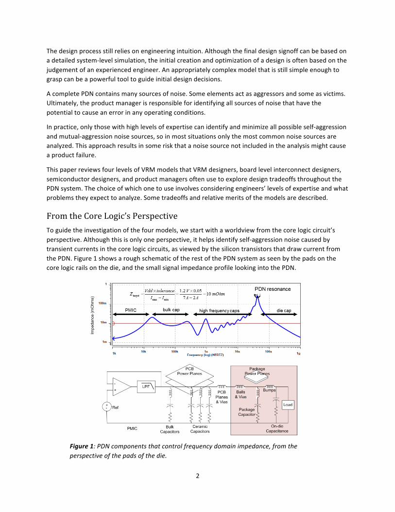
FromtheCoreLogic’sPerspectiveToguidetheinvestigationofthefourmodels,westartwithaworldviewfromthecorelogiccircuit’sperspective.Althoughthisisonlyoneperspective,ithelpsidentifyself-aggressionnoisecausedbytransientcurrentsinthecorelogiccircuits,asviewedbythesilicontransistorsthatdrawcurrentfromthePDN.Figure1showsaroughschematicoftherestofthePDNsystemasseenbythepadsonthecorelogicrailsonthedie,andthesmallsignalimpedanceprofilelookingintothePDN.
Figure1:PDNcomponentsthatcontrolfrequencydomainimpedance,fromtheperspectiveofthepadsofthedie.
3
TheVddself-aggressionnoisedependsonthepropertiesoftheboard-leveldecouplingcapacitors,boardpowerplanesandvias,thepackageballs,packagevias,powerplanesandpackagecaps,andthediebumps,theon-diepowergrid,andtheon-diecapacitanceforthesiliconloadasshowninthebottomportionofFigure1.ThisistheremainderofthePDNsystembeyondtheVRM.TheVRMisalsoknownasthepowermanagementintegratedcircuit(PMIC).
TheboardandchiplevelPDNcomponentsareimportantinthe1MHzto500MHzfrequencyband,whichisbeyondthebandwidthoftheVRMorPMICasindicatedinthetopportionofFigure1.Theboardlevelcomponentsofthebulkcap,highfrequencycaps,packagecaps,andon-diecapacitancesupplythecurrentandchargeconsumedbythesiliconloadabovethebandwidthoftheVRM.
Siliconloadsarecapableofconsumingfullcurrentstepsinjustafewclockcycles.A3GHzmicroprocessoridlingat2Amightsuddenlyrequire7Aonenanosecondlater.FaststepcurrentsmustcomefromenergyandchargestoredinPDNcapacitance.ItmustcomethroughinductivePDNstructuressuchasthediebumps,packagevias,powerplanesandballs,andboardvias,powerplanes,andcapacitormountingstructures.Eventually,severalmicrosecondslater,therequiredpowerisdeliveredfromtheVRMorPMIC.
TargetimpedanceisveryusefulfigureofmeritwhendesigningtheboardlevelPDNelementstocontrolself-aggressionnoiseonthecorelogic.Inthesituationdescribedabove,themicroprocessordemandeda5Astepcurrent(7A–2A)witha1nSecrisetime.Thevoltagetoleranceforthemicroprocessormaybe5%;thatis,itisexpectedtofunctionproperlywitha3GHzclockfrequencyifthevoltagestayswithinthe±5%tolerance.
AsimpleOhmslawcalculationrevealsthatthePDNsystemimpedanceshouldbeapproximately10mOhmswhenthenominalPDNvoltageis1.2V.Usingtheruleofthumbthatthefrequencycontentis
,thePDNshouldmeetthetargetimpedanceupto350MHz.
AllPDNsystemsoperateinthismanner.AserversystemmayrelymoreonlargeelectrolyticbulkcapacitorsandlowerbandwidthVRM,andamobilesystemmayrelyonahigherbandwidthPMICandsmallceramiccapacitors;thisisthestructureofallPDNsystemsthatsupplycurrenttosiliconloads.ItisfromthisperspectivethatwelookatsomeoftheVRMmodels.
WhatisMissingThetargetimpedanceprovidesaguidelinefordesigningPDNelements.Whenusinga5%noisetoleranceonthecorelogicrail,itisassumedallthenoiseisself-aggressionnoise.Butmutual-aggressionnoisesources,suchasvoltagetransientsfromtheVRM,orfromotherswitchingcurrentsthroughtheboardlevelimpedance,canaddtotheVddon-dierailnoise.
Thepackageleadinductanceandon-diecapacitanceactaslow-passfiltersandgenerallyfilterouthigherfrequencycomponentsfromtheboardontothedieabovethepolefrequencyoftheBandiniMountainfrequency.However,lowfrequencynoisebelow10-100MHzcanmakeitswayonthedie.Thisadditionalnoisewilladdtothe5%noisefromtheself-aggressionsources.

4
Inthisinitiallook,wewillfocusonself-aggressionnoisefromVddtransientcurrents.ThesimpleVRMmodelsintroducedtoguidethedesignofPDNsinwhichVddself-aggressionnoiseisanalyzedwillnotpredictanyofthemutual-aggressionnoise,suchastheswitchingnoisefromtheVRM,thenoisecouplingoverfromtheexternalpowersourcethatisnotblockedbythepowersupplyrejectionratio(PSRR)oftheVRM,ortheringingnoisefromthetransientresponseoftheVRMreactingtostepcurrentloadschanges.Anon-linearVRMmodelisrequiredtomodelthesesourcesofnoise,asdetailedbelow.
TheSimplestVRMModel:AnIdealVoltageSourceThesimplestVRMmodelisanidealvoltagesource.Thisrepresentationhaszerooutputresistanceandistheworstmodeltouseinanycontextbecauseitdoesnotpredictanyofthemostimportantnoisebehaviors.
Unfortunately,anidealvoltagesourceisusedtorepresenttheVRMinmanytimedomainpowerintegrity(PI)simulations.Theproblemwiththeidealvoltagesourceisthatitiszeroimpedanceandshortsout(DCandAC)anyPIcomponentitisacross.
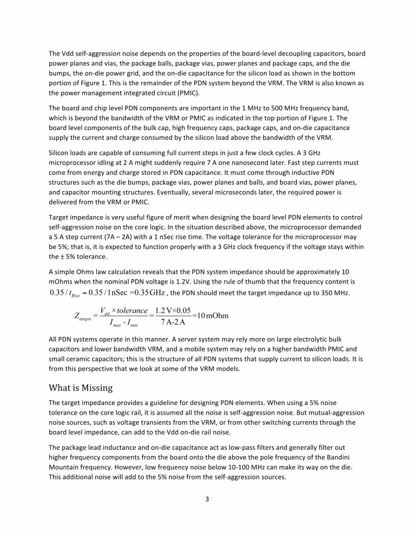
ThePIdesignflowofteninvolvesextractionofS-parametermodelsfortheprintedcircuitboard.TheextractiontooloffersportstoattachtheVRM,boardcaps,andpackagedsiliconcomponents(microprocessorload).ThenacircuitsimulationtoolusesaschematictoconnectPDNcomponentstotheportsofextractedboardandpackagemodels.AnexampleoftwomodelsisshowninFigure2.
5
Figure2:Schematicontheleftshowstheimpedancesimulationofon-diecapacitance,packageimpedance,andboardbulkcapacitance,andproducestheblueimpedancecurveonthegraph.Theschematicontherightisidentical,buthasanidealvoltagesourceshuntingtheboardcapandproducesthegreenimpedancecurve.
TheschematicontheleftinFigure2showsanimpedancemodelofsomePDNcomponents.AnACcurrentamplitudeof1Aisforcedintothe50nFon-diecapacitancewith5mOhmESR.Thereisapackageconnection(20pH,1mOhm)toaboardbulkcapacitorrepresentedbyalossytransmissionlinemodel[2].Thesimulatedimpedanceversusfrequencyforthistopologyisshowninthebluecurve(bulkcapalone).TheBandiniMountainimpedancepeakisclearlyseenat100MHz,aswellastheprofileproducedbythecapmodelandpackage.Thisisexpectedbehavior.
Softwaretoolsareoftenusedtoextracttheimpedancepropertiesofaprintedcircuitboard.ThereisatemptationtoattachanidealvoltagesourceattheextractedportterminalsfortheVRMasshownintheschematicontherightinFigure2.

6
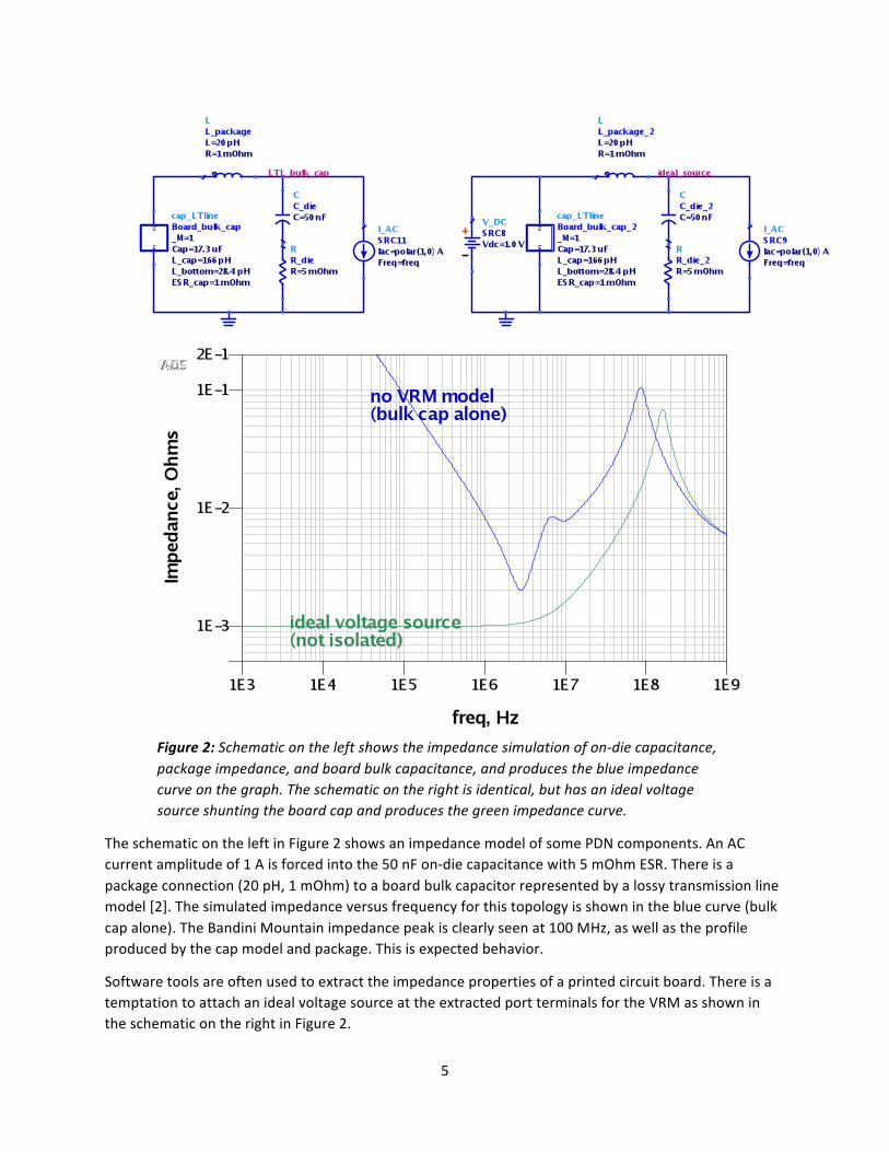
WehaveattendedmanydesignreviewsandfoundthatthistendencyofattachinganidealvoltagesourceastheVRMtotheboardlevelS-parametermodelisalltoocommon.ItisanunfortunatemistakemadebymanyPIengineers.
Attachingazero-impedancevoltagesourcetothePMICorVRMportoftheextractedPCBeffectivelyshortsoutallthePDNcomponentsontheboardwithsomesmallequivalentinductanceandresistanceassociatedwiththeboardportconnections.ThisisshownintheschematicontherightinFigure2.AsseeninthegraphinFigure2,thezero-impedanceidealvoltagesourcecreatesaflatlinebelow1MHzandeliminatesthesignatureofthebulkcap.Thebulkcaphasbeenshortedout.
ThegoalinthePDNdesignandsimulationforself-aggressionnoiseistoevaluatetheeffectivenessofbulkcaps,highfrequencycaps,boardpowerplaneconnections,andsoforth;therefore,shortingthemoutwithanidealvoltagesourceisamajorerror.Unfortunately,manyPIanalyseshavebeencorruptedbyusinganidealvoltagesource.
ItisveryimportantthatidealvoltagesourcesareneverusedinPDNsimulations,especiallywhenimpedanceortransientresponsestofaststepcurrentloadsarebeingevaluated.
AFirst-OrderLinearRLModelforaVRMThesimplestlinearmodelthatrepresentstheVRMoutputimpedancebehavior,andiscommonlyusedforfrequencydomainsimulations,isaseriesRLmodel.ThismodelhastheadvantageofbeingeasytoimplementandaccountingforsomeoftheinteractionsoftheVRMwiththerestofthePDN,fromthedie’sperspective,whensimulatingVddself-aggressionnoise.Ofcourse,thissimplemodelcannotbegintoaddressthenon-linear,stability,noiseripple,andsaturationpropertiesofarealVRM.
Figure3:RLmodelforVRM.
AsillustratedinFigure3,theoutputimpedanceriseoftheVRMduetotheinternalfeedbackresponsebandwidth,iswellrepresentedbyaninductorandresistor.TheresistorrepresentstheVRMvoltagedropthatisproportionaltoDCcurrent.Theinductorprovidesanincreasingimpedancewithfrequencybeyondsomecornerfrequency.
TheinductancevalueiscalculatedfromthecurrentrampresponsetimeorbymatchingtheresonantfrequencybetweentheVRMinductanceandbulk(output)capacitance.NotethattheinductancevalueforthesimplelinearmodelisnotrelatedtotheinductorvalueintheSMPSmodel.Theinductorofthe

7
linearRLmodelsimplycapturesthebehavioroftheregulationloop(eitherSMPSorLDO),anddoesnotrepresentanyphysicalelement.Theresistancevalue(R)intheVRMmodel(R_VRM)issimplytheresistanceatDCorsomeverylowfrequency(100Hz)atwhichtheimpedancecurvebottomsout.
AfrequencydomaincalculationfortheinductanceoftheinductorintheVRMmodel(L_VRM)isbasedonthefrequencyoftheVRMimpedancepeak.ThiscanbefoundbymeasuringtheimpedanceofaVRMsystemasafunctionoffrequency.Duetothenon-linearnatureofallVRMs,thefrequencyandheightoftheVRMimpedancepeakarenotuniqueandchangeslightlyaccordingtoloadconditions.Propertieschangefromlightlyloadedconditions(smallsignalandlinear)tofullloadtransientconditionsinwhichdampingishighlyloaddependent.Nonetheless,thefrequencyoftheVRMimpedancepeakisrelativelystable.
Figure4:Two-elementRLmodelandRLCbulkcapmodelshowhighVRMimpedancepeak.ThepeakfrequencyisusedtofindtheequivalentVRMinductance.
Figure4showsaVRMimpedancepeakatabout22kHzbecauseoftheresonancebetweenthebulkcapacitanceandtheeffectiveVRMinductance.ThecapacitanceisextractedfromthemeasuredimpedancewiththeVRMturnedoff,orfromknowledgeofthecapacitancecomponentsused.Althoughthisisthetotalon-boardcapacitance,itisdominatedbythebulkcapacitance.TheeffectiveVRMinductanceiscalculatedfromtheresonantfrequencyandon-boardcapacitance.
and
Thisistheinductanceintheresonantloopthatcausestheimpedancepeakat22kHz.TheschematicparametersindicatethatthesimulatedparameterfortheVRMwas50nHandtheinductanceofthebulkcapacitorwas2nH,thesumofwhichis52nH.ThisdemonstratesthattheresonantpeakfrequencycanbeusedtodeterminewhattheequivalentVRMinductancemusthavebeen.TheVRMresonantpeakcanbemeasured.
Itishighlydesirablethattheinductorimpedancecrossthecapacitorimpedanceexactlyatthetargetimpedanceline.Intheliterature,thisisknownasimpedancematching[3]orthecharacteristicimpedancethatgivesagoodPDNstepresponse[4].Thisimpedanceisthespecialpointatwhich

8
inductivereactancecrossesthecapacitivereactanceandthetargetimpedanceline.Wewantthe
characteristicimpedanceoftheVRMpeak, ,tobethesameasthetargetimpedanceto
keepthestepresponseatorbelowthevoltagedrooptolerance,withalowq-factortodampoutanyringing.Thisresultsinamaximallyflatimpedanceprofilethatissufficientlylowtodeliverthefulltransientcurrentwithadroopthatiswithinthevoltagetolerance.
Atimedomaincalculationoftheinductanceparametercomesfromthe property.Whentheloaddemandsafaststepofcurrent,theoutputoftheVRMislimitedbyamaximumcurrentrisetime(di/dtrate).TherisetimefortheloadfromaVddrailtransientcurrentstepisoftenexpressedinamps/nSec;thetimefortheVRMresponseisoftengiveninamps/uSec,1000timesslower.
TheequivalentinductanceforthelinearVRMmodelcanbedeterminedusingthisproperty.WhentheVRMisdrivenbyarampcurrentload,thevoltageresponseoftheVRMisameasureoftheoutputinductance.TheequivalentlargesignalinductanceoftheVRMiscalculatedfrom .InthespecialcaseinwhichtheVRMinductivereactancecrossesthecapacitivereactanceatthetargetimpedance,thevoltagedropforastepcurrentoftheworst-casetransientVddcurrentwillbethesameasthevoltagetoleranceusedinthetargetimpedancecalculation.
Figure5:TheheightoftheimpedancepeakcanbeadjustedbyincreasingVRMresistance,butthiswouldincreasetheDCresistanceandcontributetoanundesirableDCIRdrop.
TheheightoftheimpedancepeakintheparallelresonanceoftheVRMoutputinductanceandthebulkcapacitor’scapacitanceisdeterminedbysystemlosses,includingthelossesattributedtothebulkcap.ItistemptingtochooseRfora2-elementseriesRLmodeltoproperlydamptheimpedancepeak,butasshowninFigure5,thiswouldleadtoexcessiveresistanceinthepathfromtheidealvoltagesourceandtoomuchDCIRdrop.
TheRintheRLmodelneedstosatisfytwoproperties:providethecorrectdampingfortheparallelresonantpeakandprovidethecorrectDCoutputimpedance.Onesinglevaluecanrarelydothis.Amoreaccuratemodelmustincludetwovaluesofresistance,andtobeeffectiveinthecircuit,twoseriesinductorvalues.Thisisa4-elementRLmodel.
9
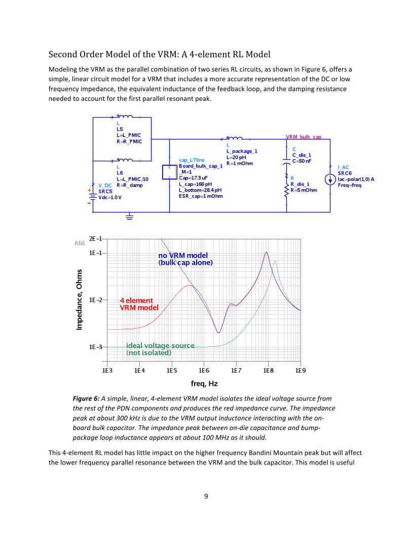
SecondOrderModeloftheVRM:A4-elementRLModelModelingtheVRMastheparallelcombinationoftwoseriesRLcircuits,asshowninFigure6,offersasimple,linearcircuitmodelforaVRMthatincludesamoreaccuraterepresentationoftheDCorlowfrequencyimpedance,theequivalentinductanceofthefeedbackloop,andthedampingresistanceneededtoaccountforthefirstparallelresonantpeak.
Figure6:Asimple,linear,4-elementVRMmodelisolatestheidealvoltagesourcefromtherestofthePDNcomponentsandproducestheredimpedancecurve.Theimpedancepeakatabout300kHzisduetotheVRMoutputinductanceinteractingwiththeon-boardbulkcapacitor.Theimpedancepeakbetweenon-diecapacitanceandbump-packageloopinductanceappearsatabout100MHzasitshould.
This4-elementRLmodelhaslittleimpactonthehigherfrequencyBandiniMountainpeakbutwillaffectthelowerfrequencyparallelresonancebetweentheVRMandthebulkcapacitor.Thismodelisuseful

10
whenanalyzingon-dieVddself-aggressionnoise.Theelementparameterscanbechosentogivereasonablyaccuratesimulationresultsinbothfrequencyandtimedomainswiththislinearmodel.
IftheVRMfeedbackpointsareinternaltotheVRM,thentheVRMmaybeattachedschematicallytotheVRMportontheextractedPCB.TheportmaybeforaSMPSinductorifthebulkcapismountedonthePCBpowerplanes.
If,however,thereareexternalfeedbacksenselinesfortheVRMthatextendtosomepointinthePDNsystem(oftensomelocationontheboardunderneathahigh-powerconsumingload),themountpointfortheVRMmodelshouldnotbeattheVRMport.SpecialPCBportsshouldbecreatedtomountthelinearVRMmodelwithlowresistanceandinductanceconnectionsclosetothesenselineterminations.
ArealVRMwithexternalsensepointswillregulatethevoltageatthesensepoints.AsimplelinearVRMmodelhasnoprovisionforfeedbackcompensation.IfthesimpleVRMmodelismountedattheextractedPCBportlocations,DCIRvoltagedropfromtheVRMporttothePCBfeedbackpointwillnotbecompensated.
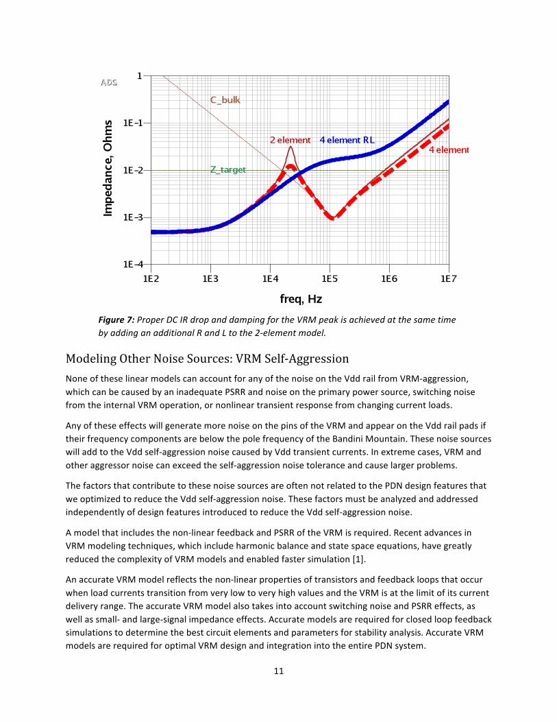
Thesecondresistor(R_damp)isusedtoindependentlydamptheimpedancepeakwhilethefirstresistorisusedtosettheproperDCIRdrop.AgoodstartingvalueforR_dampisthetargetimpedance,whichwouldresultinaq-factorof1.ThiscanberefinedbyPDNmeasurementofanactiveVRMwithaVNA.TheVRMwillnotdeliversignificantcurrentathighfrequency,soasecondinductorwithavalueofapproximatelyL_VRM/10isusedtomodeltheblockedhighfrequencycurrent.The4-elementVRMmodeldeliversthebluecurveseeninthegraphinFigure7.ItprovidesthedampingthatbringstheVRMimpedancepeakdowntothetargetimpedancewithoutimpactingtheDCIRdropatlowfrequency.
11
Figure7:ProperDCIRdropanddampingfortheVRMpeakisachievedatthesametimebyaddinganadditionalRandLtothe2-elementmodel.
ModelingOtherNoiseSources:VRMSelf-AggressionNoneoftheselinearmodelscanaccountforanyofthenoiseontheVddrailfromVRM-aggression,whichcanbecausedbyaninadequatePSRRandnoiseontheprimarypowersource,switchingnoisefromtheinternalVRMoperation,ornonlineartransientresponsefromchangingcurrentloads.
AnyoftheseeffectswillgeneratemorenoiseonthepinsoftheVRMandappearontheVddrailpadsiftheirfrequencycomponentsarebelowthepolefrequencyoftheBandiniMountain.ThesenoisesourceswilladdtotheVddself-aggressionnoisecausedbyVddtransientcurrents.Inextremecases,VRMandotheraggressornoisecanexceedtheself-aggressionnoisetoleranceandcauselargerproblems.
ThefactorsthatcontributetothesenoisesourcesareoftennotrelatedtothePDNdesignfeaturesthatweoptimizedtoreducetheVddself-aggressionnoise.ThesefactorsmustbeanalyzedandaddressedindependentlyofdesignfeaturesintroducedtoreducetheVddself-aggressionnoise.
Amodelthatincludesthenon-linearfeedbackandPSRRoftheVRMisrequired.RecentadvancesinVRMmodelingtechniques,whichincludeharmonicbalanceandstatespaceequations,havegreatlyreducedthecomplexityofVRMmodelsandenabledfastersimulation[1].
AnaccurateVRMmodelreflectsthenon-linearpropertiesoftransistorsandfeedbackloopsthatoccurwhenloadcurrentstransitionfromverylowtoveryhighvaluesandtheVRMisatthelimitofitscurrentdeliveryrange.TheaccurateVRMmodelalsotakesintoaccountswitchingnoiseandPSRReffects,aswellassmall-andlarge-signalimpedanceeffects.Accuratemodelsarerequiredforclosedloopfeedbacksimulationstodeterminethebestcircuitelementsandparametersforstabilityanalysis.AccurateVRMmodelsarerequiredforoptimalVRMdesignandintegrationintotheentirePDNsystem.
12
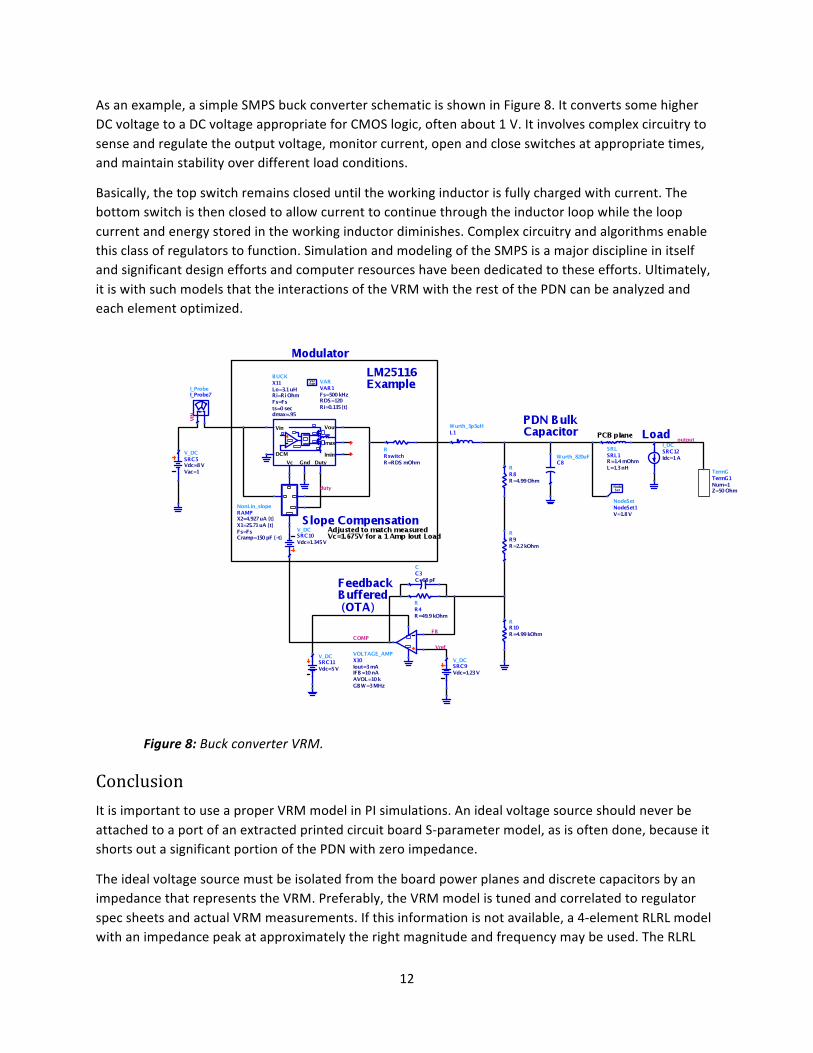
Asanexample,asimpleSMPSbuckconverterschematicisshowninFigure8.ItconvertssomehigherDCvoltagetoaDCvoltageappropriateforCMOSlogic,oftenabout1V.Itinvolvescomplexcircuitrytosenseandregulatetheoutputvoltage,monitorcurrent,openandcloseswitchesatappropriatetimes,andmaintainstabilityoverdifferentloadconditions.
Basically,thetopswitchremainscloseduntiltheworkinginductorisfullychargedwithcurrent.Thebottomswitchisthenclosedtoallowcurrenttocontinuethroughtheinductorloopwhiletheloopcurrentandenergystoredintheworkinginductordiminishes.Complexcircuitryandalgorithmsenablethisclassofregulatorstofunction.SimulationandmodelingoftheSMPSisamajordisciplineinitselfandsignificantdesigneffortsandcomputerresourceshavebeendedicatedtotheseefforts.Ultimately,itiswithsuchmodelsthattheinteractionsoftheVRMwiththerestofthePDNcanbeanalyzedandeachelementoptimized.
Figure8:BuckconverterVRM.
ConclusionItisimportanttouseaproperVRMmodelinPIsimulations.AnidealvoltagesourceshouldneverbeattachedtoaportofanextractedprintedcircuitboardS-parametermodel,asisoftendone,becauseitshortsoutasignificantportionofthePDNwithzeroimpedance.
TheidealvoltagesourcemustbeisolatedfromtheboardpowerplanesanddiscretecapacitorsbyanimpedancethatrepresentstheVRM.Preferably,theVRMmodelistunedandcorrelatedtoregulatorspecsheetsandactualVRMmeasurements.Ifthisinformationisnotavailable,a4-elementRLRLmodelwithanimpedancepeakatapproximatelytherightmagnitudeandfrequencymaybeused.TheRLRL

13
parametervaluesmaybedeterminedfromthepropertiesoftheimpedancepeak.TheVRMmodelaffectsthePDNimpedancecurveinacertainfrequencyband,often20kHzto20MHz.
AlthoughlinearmodelsfortheVRMarecriticalforoptimizingtheboardlevelPDNtomanageVddself-aggressionnoise,theycannotprovideanyinsightintonoisethatoriginateswiththeVRM.
ForacompletedescriptionofthenoiseinthePDN,includingtheVRMself-aggressionnoise,anon-linearmodelisneededandcanbeimplementedusingastatespacemodel.
References
[1] S.Sandler,HowtoDesignforPowerIntegrity:DC-DCConverterModelingandSimulation.2018.
[2] V.Sriboonlue,L.Smith,J.Mohamed,J.Shin,andT.Michalka,“NovelParallelResonancePeakMeasurementandLossyTransmissionLineModelingof2-Tand3-TMLCCcapacitorsforPDNApplication.”
[3] H.Barnes,J.Carrel,andS.Sandler,“PowerIntegrityfor32Gb/sSERDESTransceivers,”inDesignCon,2018.
[4] L.SmithandE.Bogatin,PrinciplesofPowerIntegrityforPDNDesign.PrenticeHall,2017.
[5] S.Sun,A.Corp,L.D.Smith,andP.Boyle,“On-ChipPDNNoiseCharacterizationandModeling,”inSantaClara,CA,DesignCon,2010,no.408,pp.1–21.