Embed Size (px)
Citation preview

1/38July 2004
M50FW0404 Mbit (512Kb x8, Uniform Block)
3V Supply Firmware Hub Flash Memory
FEATURES SUMMARY SUPPLY VOLTAGE
– VCC = 3V to 3.6V for Program, Erase and Read Operations
– VPP = 12V for Fast Erase (optional) TWO INTERFACES
– Firmware Hub (FWH) Interface for embedded operation with PC Chipsets.
– Address/Address Multiplexed (A/A Mux) Interface for programming equipment compatibility.
FIRMWARE HUB (FWH) HARDWARE INTERFACE MODE– 5 Signal Communication Interface
supporting Read and Write Operations– Hardware Write Protect Pins for Block
Protection– Register Based Read and Write
Protection– 5 Additional General Purpose Inputs for
platform design flexibility– Synchronized with 33MHz PCI clock
PROGRAMMING TIME: 10µs typical 8 UNIFORM 64 Kbyte MEMORY BLOCKS PROGRAM/ERASE CONTROLLER
– Embedded Byte Program and Block Erase algorithms
– Status Register Bits PROGRAM and ERASE SUSPEND
– Read other Blocks during Program/Erase Suspend
– Program other Blocks during Erase Suspend
FOR USE in PC BIOS APPLICATIONS ELECTRONIC SIGNATURE
– Manufacturer Code: 20h– Device Code: 2Ch
Figure 1. Packages
TSOP40 (N)10 x 20mm
PLCC32 (K)

M50FW040
2/38
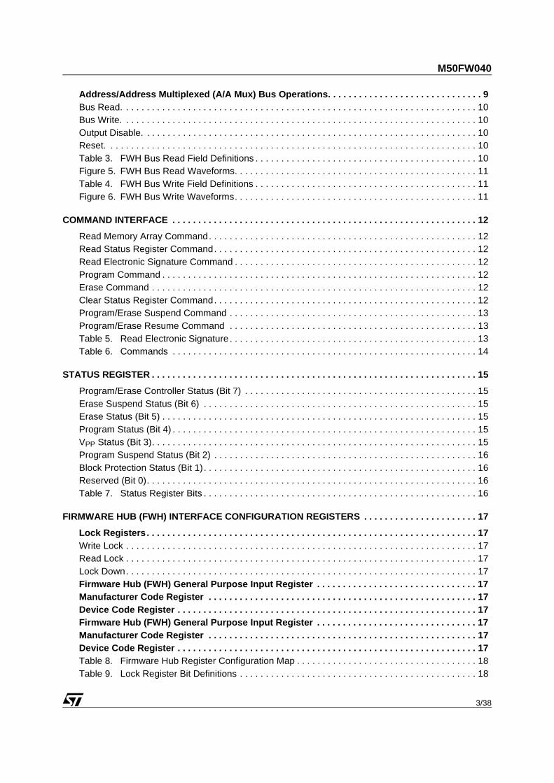
TABLE OF CONTENTS
FEATURES SUMMARY . . . . . . . . . . . . . . . . . . . . . . . . . . . . . . . . . . . . . . . . . . . . . . . . . . . . . . . . . . . . . 1
Figure 1. Packages . . . . . . . . . . . . . . . . . . . . . . . . . . . . . . . . . . . . . . . . . . . . . . . . . . . . . . . . . . . . . . 1
SUMMARY DESCRIPTION. . . . . . . . . . . . . . . . . . . . . . . . . . . . . . . . . . . . . . . . . . . . . . . . . . . . . . . . . . . 5
Figure 2. Logic Diagram (FWH Interface) . . . . . . . . . . . . . . . . . . . . . . . . . . . . . . . . . . . . . . . . . . . . . 5Table 1. Signal Names (FWH Interface) . . . . . . . . . . . . . . . . . . . . . . . . . . . . . . . . . . . . . . . . . . . . . 5Figure 3. PLCC Connections . . . . . . . . . . . . . . . . . . . . . . . . . . . . . . . . . . . . . . . . . . . . . . . . . . . . . . 6Figure 4. TSOP Connections . . . . . . . . . . . . . . . . . . . . . . . . . . . . . . . . . . . . . . . . . . . . . . . . . . . . . . 6
SIGNAL DESCRIPTIONS . . . . . . . . . . . . . . . . . . . . . . . . . . . . . . . . . . . . . . . . . . . . . . . . . . . . . . . . . . . . 7
Firmware Hub (FWH) Signal Descriptions . . . . . . . . . . . . . . . . . . . . . . . . . . . . . . . . . . . . . . . . . . 7Input/Output Communications (FWH0-FWH3). . . . . . . . . . . . . . . . . . . . . . . . . . . . . . . . . . . . . . . . . . 7Input Communication Frame (FWH4).. . . . . . . . . . . . . . . . . . . . . . . . . . . . . . . . . . . . . . . . . . . . . . . . 7Identification Inputs (ID0-ID3). . . . . . . . . . . . . . . . . . . . . . . . . . . . . . . . . . . . . . . . . . . . . . . . . . . . . . . 7General Purpose Inputs (FGPI0-FGPI4). . . . . . . . . . . . . . . . . . . . . . . . . . . . . . . . . . . . . . . . . . . . . . 7Interface Configuration (IC). . . . . . . . . . . . . . . . . . . . . . . . . . . . . . . . . . . . . . . . . . . . . . . . . . . . . . . . 7Interface Reset (RP). . . . . . . . . . . . . . . . . . . . . . . . . . . . . . . . . . . . . . . . . . . . . . . . . . . . . . . . . . . . . . 7CPU Reset (INIT). . . . . . . . . . . . . . . . . . . . . . . . . . . . . . . . . . . . . . . . . . . . . . . . . . . . . . . . . . . . . . . . 7Clock (CLK). . . . . . . . . . . . . . . . . . . . . . . . . . . . . . . . . . . . . . . . . . . . . . . . . . . . . . . . . . . . . . . . . . . . 7Top Block Lock (TBL). . . . . . . . . . . . . . . . . . . . . . . . . . . . . . . . . . . . . . . . . . . . . . . . . . . . . . . . . . . . . 7Write Protect (WP). . . . . . . . . . . . . . . . . . . . . . . . . . . . . . . . . . . . . . . . . . . . . . . . . . . . . . . . . . . . . . . 7Reserved for Future Use (RFU). . . . . . . . . . . . . . . . . . . . . . . . . . . . . . . . . . . . . . . . . . . . . . . . . . . . . 8Address/Address Multiplexed (A/A Mux) Signal Descriptions . . . . . . . . . . . . . . . . . . . . . . . . . . 8Address Inputs (A0-A10). . . . . . . . . . . . . . . . . . . . . . . . . . . . . . . . . . . . . . . . . . . . . . . . . . . . . . . . . . 8Data Inputs/Outputs (DQ0-DQ7). . . . . . . . . . . . . . . . . . . . . . . . . . . . . . . . . . . . . . . . . . . . . . . . . . . . 8Output Enable (G). . . . . . . . . . . . . . . . . . . . . . . . . . . . . . . . . . . . . . . . . . . . . . . . . . . . . . . . . . . . . . . 8Write Enable (W). . . . . . . . . . . . . . . . . . . . . . . . . . . . . . . . . . . . . . . . . . . . . . . . . . . . . . . . . . . . . . . . 8Row/Column Address Select (RC). . . . . . . . . . . . . . . . . . . . . . . . . . . . . . . . . . . . . . . . . . . . . . . . . . . 8Ready/Busy Output (RB). . . . . . . . . . . . . . . . . . . . . . . . . . . . . . . . . . . . . . . . . . . . . . . . . . . . . . . . . . 8Supply Signal Descriptions . . . . . . . . . . . . . . . . . . . . . . . . . . . . . . . . . . . . . . . . . . . . . . . . . . . . . . 8VCC Supply Voltage. . . . . . . . . . . . . . . . . . . . . . . . . . . . . . . . . . . . . . . . . . . . . . . . . . . . . . . . . . . . . . 8VPP Optional Supply Voltage. . . . . . . . . . . . . . . . . . . . . . . . . . . . . . . . . . . . . . . . . . . . . . . . . . . . . . . 8VSS Ground. . . . . . . . . . . . . . . . . . . . . . . . . . . . . . . . . . . . . . . . . . . . . . . . . . . . . . . . . . . . . . . . . . . . 8Table 2. Block Addresses . . . . . . . . . . . . . . . . . . . . . . . . . . . . . . . . . . . . . . . . . . . . . . . . . . . . . . . . 8
BUS OPERATIONS. . . . . . . . . . . . . . . . . . . . . . . . . . . . . . . . . . . . . . . . . . . . . . . . . . . . . . . . . . . . . . . . . 9
Firmware Hub (FWH) Bus Operations . . . . . . . . . . . . . . . . . . . . . . . . . . . . . . . . . . . . . . . . . . . . . . 9Bus Read. . . . . . . . . . . . . . . . . . . . . . . . . . . . . . . . . . . . . . . . . . . . . . . . . . . . . . . . . . . . . . . . . . . . . . 9Bus Write. . . . . . . . . . . . . . . . . . . . . . . . . . . . . . . . . . . . . . . . . . . . . . . . . . . . . . . . . . . . . . . . . . . . . . 9Bus Abort. . . . . . . . . . . . . . . . . . . . . . . . . . . . . . . . . . . . . . . . . . . . . . . . . . . . . . . . . . . . . . . . . . . . . . 9Standby. . . . . . . . . . . . . . . . . . . . . . . . . . . . . . . . . . . . . . . . . . . . . . . . . . . . . . . . . . . . . . . . . . . . . . . 9Reset. . . . . . . . . . . . . . . . . . . . . . . . . . . . . . . . . . . . . . . . . . . . . . . . . . . . . . . . . . . . . . . . . . . . . . . . . 9Block Protection. . . . . . . . . . . . . . . . . . . . . . . . . . . . . . . . . . . . . . . . . . . . . . . . . . . . . . . . . . . . . . . . . 9
3/38
M50FW040
Address/Address Multiplexed (A/A Mux) Bus Operations. . . . . . . . . . . . . . . . . . . . . . . . . . . . . . 9Bus Read. . . . . . . . . . . . . . . . . . . . . . . . . . . . . . . . . . . . . . . . . . . . . . . . . . . . . . . . . . . . . . . . . . . . . 10Bus Write. . . . . . . . . . . . . . . . . . . . . . . . . . . . . . . . . . . . . . . . . . . . . . . . . . . . . . . . . . . . . . . . . . . . . 10Output Disable. . . . . . . . . . . . . . . . . . . . . . . . . . . . . . . . . . . . . . . . . . . . . . . . . . . . . . . . . . . . . . . . . 10Reset. . . . . . . . . . . . . . . . . . . . . . . . . . . . . . . . . . . . . . . . . . . . . . . . . . . . . . . . . . . . . . . . . . . . . . . . 10Table 3. FWH Bus Read Field Definitions . . . . . . . . . . . . . . . . . . . . . . . . . . . . . . . . . . . . . . . . . . . 10Figure 5. FWH Bus Read Waveforms. . . . . . . . . . . . . . . . . . . . . . . . . . . . . . . . . . . . . . . . . . . . . . . 11Table 4. FWH Bus Write Field Definitions . . . . . . . . . . . . . . . . . . . . . . . . . . . . . . . . . . . . . . . . . . . 11Figure 6. FWH Bus Write Waveforms. . . . . . . . . . . . . . . . . . . . . . . . . . . . . . . . . . . . . . . . . . . . . . . 11
COMMAND INTERFACE . . . . . . . . . . . . . . . . . . . . . . . . . . . . . . . . . . . . . . . . . . . . . . . . . . . . . . . . . . . 12
Read Memory Array Command. . . . . . . . . . . . . . . . . . . . . . . . . . . . . . . . . . . . . . . . . . . . . . . . . . . . 12Read Status Register Command. . . . . . . . . . . . . . . . . . . . . . . . . . . . . . . . . . . . . . . . . . . . . . . . . . . 12Read Electronic Signature Command . . . . . . . . . . . . . . . . . . . . . . . . . . . . . . . . . . . . . . . . . . . . . . . 12Program Command . . . . . . . . . . . . . . . . . . . . . . . . . . . . . . . . . . . . . . . . . . . . . . . . . . . . . . . . . . . . . 12Erase Command . . . . . . . . . . . . . . . . . . . . . . . . . . . . . . . . . . . . . . . . . . . . . . . . . . . . . . . . . . . . . . . 12Clear Status Register Command. . . . . . . . . . . . . . . . . . . . . . . . . . . . . . . . . . . . . . . . . . . . . . . . . . . 12Program/Erase Suspend Command . . . . . . . . . . . . . . . . . . . . . . . . . . . . . . . . . . . . . . . . . . . . . . . . 13Program/Erase Resume Command . . . . . . . . . . . . . . . . . . . . . . . . . . . . . . . . . . . . . . . . . . . . . . . . 13Table 5. Read Electronic Signature . . . . . . . . . . . . . . . . . . . . . . . . . . . . . . . . . . . . . . . . . . . . . . . . 13Table 6. Commands . . . . . . . . . . . . . . . . . . . . . . . . . . . . . . . . . . . . . . . . . . . . . . . . . . . . . . . . . . . 14
STATUS REGISTER . . . . . . . . . . . . . . . . . . . . . . . . . . . . . . . . . . . . . . . . . . . . . . . . . . . . . . . . . . . . . . . 15
Program/Erase Controller Status (Bit 7) . . . . . . . . . . . . . . . . . . . . . . . . . . . . . . . . . . . . . . . . . . . . . 15Erase Suspend Status (Bit 6) . . . . . . . . . . . . . . . . . . . . . . . . . . . . . . . . . . . . . . . . . . . . . . . . . . . . . 15Erase Status (Bit 5) . . . . . . . . . . . . . . . . . . . . . . . . . . . . . . . . . . . . . . . . . . . . . . . . . . . . . . . . . . . . . 15Program Status (Bit 4) . . . . . . . . . . . . . . . . . . . . . . . . . . . . . . . . . . . . . . . . . . . . . . . . . . . . . . . . . . . 15VPP Status (Bit 3). . . . . . . . . . . . . . . . . . . . . . . . . . . . . . . . . . . . . . . . . . . . . . . . . . . . . . . . . . . . . . . 15Program Suspend Status (Bit 2) . . . . . . . . . . . . . . . . . . . . . . . . . . . . . . . . . . . . . . . . . . . . . . . . . . . 16Block Protection Status (Bit 1) . . . . . . . . . . . . . . . . . . . . . . . . . . . . . . . . . . . . . . . . . . . . . . . . . . . . . 16Reserved (Bit 0). . . . . . . . . . . . . . . . . . . . . . . . . . . . . . . . . . . . . . . . . . . . . . . . . . . . . . . . . . . . . . . . 16Table 7. Status Register Bits . . . . . . . . . . . . . . . . . . . . . . . . . . . . . . . . . . . . . . . . . . . . . . . . . . . . . 16
FIRMWARE HUB (FWH) INTERFACE CONFIGURATION REGISTERS . . . . . . . . . . . . . . . . . . . . . . 17
Lock Registers. . . . . . . . . . . . . . . . . . . . . . . . . . . . . . . . . . . . . . . . . . . . . . . . . . . . . . . . . . . . . . . . 17Write Lock . . . . . . . . . . . . . . . . . . . . . . . . . . . . . . . . . . . . . . . . . . . . . . . . . . . . . . . . . . . . . . . . . . . . 17Read Lock . . . . . . . . . . . . . . . . . . . . . . . . . . . . . . . . . . . . . . . . . . . . . . . . . . . . . . . . . . . . . . . . . . . . 17Lock Down. . . . . . . . . . . . . . . . . . . . . . . . . . . . . . . . . . . . . . . . . . . . . . . . . . . . . . . . . . . . . . . . . . . . 17Firmware Hub (FWH) General Purpose Input Register . . . . . . . . . . . . . . . . . . . . . . . . . . . . . . . 17Manufacturer Code Register . . . . . . . . . . . . . . . . . . . . . . . . . . . . . . . . . . . . . . . . . . . . . . . . . . . . 17Device Code Register . . . . . . . . . . . . . . . . . . . . . . . . . . . . . . . . . . . . . . . . . . . . . . . . . . . . . . . . . . 17Firmware Hub (FWH) General Purpose Input Register . . . . . . . . . . . . . . . . . . . . . . . . . . . . . . . 17Manufacturer Code Register . . . . . . . . . . . . . . . . . . . . . . . . . . . . . . . . . . . . . . . . . . . . . . . . . . . . 17Device Code Register . . . . . . . . . . . . . . . . . . . . . . . . . . . . . . . . . . . . . . . . . . . . . . . . . . . . . . . . . . 17Table 8. Firmware Hub Register Configuration Map . . . . . . . . . . . . . . . . . . . . . . . . . . . . . . . . . . . 18Table 9. Lock Register Bit Definitions . . . . . . . . . . . . . . . . . . . . . . . . . . . . . . . . . . . . . . . . . . . . . . 18

M50FW040
4/38
Table 10. General Purpose Inputs Register Definition . . . . . . . . . . . . . . . . . . . . . . . . . . . . . . . . . . 18
PROGRAM AND ERASE TIMES . . . . . . . . . . . . . . . . . . . . . . . . . . . . . . . . . . . . . . . . . . . . . . . . . . . . . 19
Table 11. Program and Erase Times. . . . . . . . . . . . . . . . . . . . . . . . . . . . . . . . . . . . . . . . . . . . . . . . 19
MAXIMUM RATING. . . . . . . . . . . . . . . . . . . . . . . . . . . . . . . . . . . . . . . . . . . . . . . . . . . . . . . . . . . . . . . . 20
Table 12. Absolute Maximum Ratings . . . . . . . . . . . . . . . . . . . . . . . . . . . . . . . . . . . . . . . . . . . . . . . 20
DC AND AC PARAMETERS. . . . . . . . . . . . . . . . . . . . . . . . . . . . . . . . . . . . . . . . . . . . . . . . . . . . . . . . . 21
Table 13. Operating Conditions. . . . . . . . . . . . . . . . . . . . . . . . . . . . . . . . . . . . . . . . . . . . . . . . . . . . 21Table 14. FWH Interface AC Measurement Conditions. . . . . . . . . . . . . . . . . . . . . . . . . . . . . . . . . . 21Table 15. A/A Mux Interface AC Measurement Conditions . . . . . . . . . . . . . . . . . . . . . . . . . . . . . . . 21Figure 7. FWH Interface AC Testing Input Output Waveforms. . . . . . . . . . . . . . . . . . . . . . . . . . . . 21Figure 8. A/A Mux Interface AC Testing Input Output Waveform . . . . . . . . . . . . . . . . . . . . . . . . . . 22Table 16. Impedance. . . . . . . . . . . . . . . . . . . . . . . . . . . . . . . . . . . . . . . . . . . . . . . . . . . . . . . . . . . . 22Table 17. DC Characteristics. . . . . . . . . . . . . . . . . . . . . . . . . . . . . . . . . . . . . . . . . . . . . . . . . . . . . . 23Figure 9. FWH Interface Clock Waveform . . . . . . . . . . . . . . . . . . . . . . . . . . . . . . . . . . . . . . . . . . . 24Table 18. FWH Interface Clock Characteristics. . . . . . . . . . . . . . . . . . . . . . . . . . . . . . . . . . . . . . . . 24Figure 10.FWH Interface AC Signal Timing Waveforms . . . . . . . . . . . . . . . . . . . . . . . . . . . . . . . . . 25Table 19. FWH Interface AC Signal Timing Characteristics . . . . . . . . . . . . . . . . . . . . . . . . . . . . . . 25Figure 11.Reset AC Waveforms . . . . . . . . . . . . . . . . . . . . . . . . . . . . . . . . . . . . . . . . . . . . . . . . . . . 26Table 20. Reset AC Characteristics. . . . . . . . . . . . . . . . . . . . . . . . . . . . . . . . . . . . . . . . . . . . . . . . . 26Figure 12.A/A Mux Interface Read AC Waveforms . . . . . . . . . . . . . . . . . . . . . . . . . . . . . . . . . . . . . 27Table 21. A/A Mux Interface Read AC Characteristics . . . . . . . . . . . . . . . . . . . . . . . . . . . . . . . . . . 27Figure 13.A/A Mux Interface Write AC Waveforms . . . . . . . . . . . . . . . . . . . . . . . . . . . . . . . . . . . . . 28Table 22. A/A Mux Interface Write AC Characteristics . . . . . . . . . . . . . . . . . . . . . . . . . . . . . . . . . . 28
PACKAGE MECHANICAL . . . . . . . . . . . . . . . . . . . . . . . . . . . . . . . . . . . . . . . . . . . . . . . . . . . . . . . . . . 29
Figure 14.PLCC32 – 32 pin Rectangular Plastic Leaded Chip Carrier, Package Outline . . . . . . . . 29Table 23. PLCC32 – 32 pin Rectangular Plastic Leaded Chip Carrier, Package Mechanical Data 30Figure 15.TSOP40 – 40 lead Plastic Thin Small Outline, 10x20 mm, Package Outline . . . . . . . . . 31Table 24. TSOP40 – 40 lead Plastic Thin Small Outline, 10x20 mm, Package Mechanical Data. . 31
PART NUMBERING . . . . . . . . . . . . . . . . . . . . . . . . . . . . . . . . . . . . . . . . . . . . . . . . . . . . . . . . . . . . . . . 32
Table 25. Ordering Information Scheme . . . . . . . . . . . . . . . . . . . . . . . . . . . . . . . . . . . . . . . . . . . . . 32
FLOWCHARTS AND PSEUDO CODES. . . . . . . . . . . . . . . . . . . . . . . . . . . . . . . . . . . . . . . . . . . . . . . . 33
Figure 16.Program Flowchart and Pseudo Code . . . . . . . . . . . . . . . . . . . . . . . . . . . . . . . . . . . . . . 33Figure 17.Program Suspend & Resume Flowchart and Pseudo Code . . . . . . . . . . . . . . . . . . . . . . 34Figure 18.Erase Flowchart and Pseudo Code. . . . . . . . . . . . . . . . . . . . . . . . . . . . . . . . . . . . . . . . . 35Figure 19.Erase Suspend & Resume Flowchart and Pseudo Code . . . . . . . . . . . . . . . . . . . . . . . . 36
REVISION HISTORY. . . . . . . . . . . . . . . . . . . . . . . . . . . . . . . . . . . . . . . . . . . . . . . . . . . . . . . . . . . . . . . 37
Table 26. Document Revision History . . . . . . . . . . . . . . . . . . . . . . . . . . . . . . . . . . . . . . . . . . . . . . . 37

5/38
M50FW040
SUMMARY DESCRIPTIONThe M50FW040 is a 4 Mbit (512Kb x8) non-vola-tile memory that can be read, erased and repro-grammed. These operations can be performedusing a single low voltage (3.0 to 3.6V) supply. Forfast erasing in production lines an optional 12Vpower supply can be used to reduce the erasingtime.The memory is divided into blocks that can beerased independently so it is possible to preservevalid data while old data is erased. Blocks can beprotected individually to prevent accidental Pro-gram or Erase commands from modifying thememory. Program and Erase commands are writ-ten to the Command Interface of the memory. Anon-chip Program/Erase Controller simplifies theprocess of programming or erasing the memory bytaking care of all of the special operations that arerequired to update the memory contents. The endof a program or erase operation can be detected
and any error conditions identified. The commandset required to control the memory is consistentwith JEDEC standards.Two different bus interfaces are supported by thememory. The primary interface, the Firmware Hub(or FWH) Interface, uses Intel’s proprietary FWHprotocol. This has been designed to remove theneed for the ISA bus in current PC Chipsets; theM50FW040 acts as the PC BIOS on the Low PinCount bus for these PC Chipsets.The secondary interface, the Address/AddressMultiplexed (or A/A Mux) Interface, is designed tobe compatible with current Flash Programmers forproduction line programming prior to fitting to a PCMotherboard.The memory is offered in TSOP40 (10 x 20mm)and PLCC32 packages and it is supplied with allthe bits erased (set to ’1’).
Figure 2. Logic Diagram (FWH Interface) Table 1. Signal Names (FWH Interface)
AI03623
4
FWH4
FWH0-FWH3
VCC
M50FW040
CLK
VSS
4
IC
RP
TBL
5
INIT
WP
ID0-ID3
FGPI0-FGPI4
VPP
FWH0-FWH3 Input/Output Communications
FWH4 Input Communication Frame
ID0-ID3 Identification Inputs
FGPI0-FGPI4 General Purpose Inputs
IC Interface Configuration
RP Interface Reset
INIT CPU Reset
CLK Clock
TBL Top Block Lock
WP Write Protect
RFU Reserved for Future Use. Leave disconnected
VCC Supply Voltage
VPPOptional Supply Voltage for Fast Erase Operations
VSS Ground
NC Not Connected Internally

M50FW040
6/38
Figure 3. PLCC Connections
Note: Pins 27 and 28 are not internally connected.
Figure 4. TSOP Connections
AI03616
FG
PI4
NC
FWH4
RF
U17
ID1ID0
FWH0
FW
H1
FW
H2
FW
H3
RF
U
FGPI1
TBLID3ID2
FGPI0WP
9
CLK
VSS
1
RP
VCC
NC
FG
PI2
RFU
32
VP
PV
CC
M50FW040F
GP
I3
IC (VIL)
RF
U
INIT
RFU
25
VS
SA1A0
DQ0
A7
A4A3A2
A6A5
A10
RC
RP
A8
VP
PV
CC
A9
NC
W
VSSVCC
NC
DQ7
IC (VIH)
G
RB
DQ
5
DQ
1D
Q2
DQ
3D
Q4
DQ
6
VS
S
A/A Mux A/A Mux
A/A MuxA/A Mux
AI03617
A1A0DQ0
A7
A4 A3A2
A6A5
A9A8
W
VSSVCC
DQ7
GRB
DQ5
DQ1DQ2DQ3
DQ4
DQ6
A/A
Mux
A/A
Mux
ID1
FWH1FWH2
FGPI3
TBLID2
FGPI0WP
NC
VCCNC
IC (VIL)
RFUFGPI4
NC
VSS
FWH4
RFU
FWH3VSS
VCC
RFU
RFUNC
CLK
RP
NC
VPP
VCC
NC
M50FW04010
1
11
20 21
3031
40
ID3
NC INITNC RFU
FGPI2 FWH0FGPI1 ID0
VSSNC
NC
NCIC (VIH)
NCNC
NCNC
RC
RPVPP
VCC
NCA10
VSSVSS
VCC

7/38
M50FW040
SIGNAL DESCRIPTIONSThere are two different bus interfaces available onthis part. The active interface is selected beforepower-up or during Reset using the Interface Con-figuration Pin, IC.The signals for each interface are discussed in theFirmware Hub (FWH) Signal Descriptions sectionand the Address/Address Multiplexed (A/A Mux)Signal Descriptions section below. The supply sig-nals are discussed in the Supply Signal Descrip-tions section below.Firmware Hub (FWH) Signal DescriptionsFor the Firmware Hub (FWH) Interface see Figure2., Logic Diagram (FWH Interface), and Table1., Signal Names (FWH Interface).Input/Output Communications (FWH0-FWH3). AllInput and Output Communication with the memorytake place on these pins. Addresses and Data forBus Read and Bus Write operations are encodedon these pins.Input Communication Frame (FWH4). The In-put Communication Frame (FWH4) signals thestart of a bus operation. When Input Communica-tion Frame is Low, VIL, on the rising edge of theClock a new bus operation is initiated. If InputCommunication Frame is Low, VIL, during a busoperation then the operation is aborted. When In-put Communication Frame is High, VIH, the cur-rent bus operation is proceeding or the bus is idle.Identification Inputs (ID0-ID3). The Identifica-tion Inputs select the address that the memory re-sponds to. Up to 16 memories can be addressedon a bus. For an address bit to be ‘0’ the pin canbe left floating or driven Low, VIL; an internal pull-down resistor is included with a value of RIL. Foran address bit to be ‘1’ the pin must be drivenHigh, VIH; there will be a leakage current of ILI2through each pin when pulled to VIH; see Table 17.By convention the boot memory must have ad-dress ‘0000’ and all additional memories take se-quential addresses starting from ‘0001’.General Purpose Inputs (FGPI0-FGPI4). The Gen-eral Purpose Inputs can be used as digital inputsfor the CPU to read. The General Purpose InputsRegister holds the values on these pins. The pinsmust have stable data from before the start of thecycle that reads the General Purpose Input Regis-ter until after the cycle is complete. These pinsmust not be left to float, they should be driven Low,VIL, or High, VIH.Interface Configuration (IC). The Interface Con-figuration input selects whether the Firmware Hub(FWH) or the Address/Address Multiplexed (A/AMux) Interface is used. The chosen interface mustbe selected before power-up or during a Resetand, thereafter, cannot be changed. The state of
the Interface Configuration, IC, should not bechanged during operation.To select the Firmware Hub (FWH) Interface theInterface Configuration pin should be left to float ordriven Low, VIL; to select the Address/AddressMultiplexed (A/A Mux) Interface the pin should bedriven High, VIH. An internal pull-down resistor isincluded with a value of RIL; there will be a leakagecurrent of ILI2 through each pin when pulled to VIH;see Table 17.Interface Reset (RP). The Interface Reset (RP)input is used to reset the memory. When InterfaceReset (RP) is set Low, VIL, the memory is in Resetmode: the outputs are put to high impedance andthe current consumption is minimized. When RP isset High, VIH, the memory is in normal operation.After exiting Reset mode, the memory entersRead mode.CPU Reset (INIT). The CPU Reset, INIT, pin isused to Reset the memory when the CPU is reset.It behaves identically to Interface Reset, RP, andthe internal Reset line is the logical OR (electricalAND) of RP and INIT.Clock (CLK). The Clock, CLK, input is used toclock the signals in and out of the Input/OutputCommunication Pins, FWH0-FWH3. The Clockconforms to the PCI specification.Top Block Lock (TBL). The Top Block Lock in-put is used to prevent the Top Block (Block 7) frombeing changed. When Top Block Lock, TBL, is setLow, VIL, Program and Erase operations in theTop Block have no effect, regardless of the stateof the Lock Register. When Top Block Lock, TBL,is set High, VIH, the protection of the Block is de-termined by the Lock Register. The state of TopBlock Lock, TBL, does not affect the protection ofthe Main Blocks (Blocks 0 to 6).Top Block Lock, TBL, must be set prior to a Pro-gram or Erase operation is initiated and must notbe changed until the operation completes or un-predictable results may occur. Care should be tak-en to avoid unpredictable behavior by changingTBL during Program or Erase Suspend.Write Protect (WP). The Write Protect input isused to prevent the Main Blocks (Blocks 0 to 6)from being changed. When Write Protect, WP, isset Low, VIL, Program and Erase operations in theMain Blocks have no effect, regardless of the stateof the Lock Register. When Write Protect, WP, isset High, VIH, the protection of the Block deter-mined by the Lock Register. The state of WriteProtect, WP, does not affect the protection of theTop Block (Block 7). Write Protect, WP, must be set prior to a Programor Erase operation is initiated and must not bechanged until the operation completes or unpre-

M50FW040
8/38
dictable results may occur. Care should be takento avoid unpredictable behavior by changing WPduring Program or Erase Suspend.Reserved for Future Use (RFU). These pins donot have assigned functions in this revision of thepart. They must be left disconnected.Address/Address Multiplexed (A/A Mux) Signal DescriptionsFor the Address/Address Multiplexed (A/A Mux)Interface see Figure 2., Logic Diagram (FWH In-terface), and Table 1., Signal Names (FWH Inter-face).Address Inputs (A0-A10). The Address Inputsare used to set the Row Address bits (A0-A10) andthe Column Address bits (A11-A18). They arelatched during any bus operation by the Row/Col-umn Address Select input, RC.Data Inputs/Outputs (DQ0-DQ7). The Data In-puts/Outputs hold the data that is written to or readfrom the memory. They output the data stored atthe selected address during a Bus Read opera-tion. During Bus Write operations they representthe commands sent to the Command Interface ofthe internal state machine. The Data Inputs/Out-puts, DQ0-DQ7, are latched during a Bus Writeoperation.Output Enable (G). The Output Enable, G, con-trols the Bus Read operation of the memory.Write Enable (W). The Write Enable, W, controlsthe Bus Write operation of the memory’s Com-mand Interface.Row/Column Address Select (RC). The Row/Column Address Select input selects whether theAddress Inputs should be latched into the Row Ad-dress bits (A0-A10) or the Column Address bits(A11-A18). The Row Address bits are latched onthe falling edge of RC whereas the Column Ad-dress bits are latched on the rising edge.Ready/Busy Output (RB). The Ready/Busy pingives the status of the memory’s Program/EraseController. When Ready/Busy is Low, VOL, thememory is busy with a Program or Erase operationand it will not accept any additional Program orErase command except the Program/Erase Sus-pend command. When Ready/Busy is High, VOH,the memory is ready for any Read, Program orErase operation.Supply Signal DescriptionsThe Supply Signals are the same for both interfac-es.
VCC Supply Voltage. The VCC Supply Voltagesupplies the power for all operations (Read, Pro-gram, Erase etc.).The Command Interface is disabled when the VCCSupply Voltage is less than the Lockout Voltage,VLKO. This prevents Bus Write operations from ac-cidentally damaging the data during power up,power down and power surges. If the Program/Erase Controller is programming or erasing duringthis time then the operation aborts and the memo-ry contents being altered will be invalid. After VCCbecomes valid the Command Interface is reset toRead mode.A 0.1µF capacitor should be connected betweenthe VCC Supply Voltage pins and the VSS Groundpin to decouple the current surges from the powersupply. Both VCC Supply Voltage pins must beconnected to the power supply. The PCB trackwidths must be sufficient to carry the currents re-quired during program and erase operations.VPP Optional Supply Voltage. The VPP OptionalSupply Voltage pin is used to select the Fast Eraseoption of the memory and to protect the memory.When VPP < VPPLK Program and Erase operationscannot be performed and an error is reported inthe Status Register if an attempt to change thememory contents is made. When VPP = VCC Pro-gram and Erase operations take place as normal.When VPP = VPPH Fast Erase operations areused. Any other voltage input to VPP will result inundefined behavior and should not be used.VPP should not be set to VPPH for more than 80hours during the life of the memory.VSS Ground. VSS is the reference for all the volt-age measurements.
Table 2. Block AddressesSize
(Kbytes) Address Range Block Number Block Type
64 70000h-7FFFFh 7 Top Block
64 60000h-6FFFFh 6 Main Block
64 50000h-5FFFFh 5 Main Block
64 40000h-4FFFFh 4 Main Block
64 30000h-3FFFFh 3 Main Block
64 20000h-2FFFFh 2 Main Block
64 10000h-1FFFFh 1 Main Block
64 00000h-0FFFFh 0 Main Block

9/38
M50FW040
BUS OPERATIONSThe two interfaces have similar bus operations butthe signals and timings are completely different.The Firmware Hub (FWH) Interface is the usual in-terface and all of the functionality of the part isavailable through this interface. Only a subset offunctions are available through the Address/Ad-dress Multiplexed (A/A Mux) Interface.Follow the section Firmware Hub (FWH) Bus Op-erations below and the section Address/AddressMultiplexed (A/A Mux) Bus Operations below for adescription of the bus operations on each inter-face.Firmware Hub (FWH) Bus OperationsThe Firmware Hub (FWH) Interface consists offour data signals (FWH0-FWH3), one control line(FWH4) and a clock (CLK). In addition protectionagainst accidental or malicious data corruptioncan be achieved using two further signals (TBLand WP). Finally two reset signals (RP and INIT)are available to put the memory into a knownstate.The data signals, control signal and clock are de-signed to be compatible with PCI electrical specifi-cations. The interface operates with clock speedsup to 33MHz.The following operations can be performed usingthe appropriate bus cycles: Bus Read, Bus Write,Standby, Reset and Block Protection.Bus Read. Bus Read operations read from thememory cells, specific registers in the CommandInterface or Firmware Hub Registers. A valid BusRead operation starts when Input CommunicationFrame, FWH4, is Low, VIL, as Clock rises and thecorrect Start cycle is on FWH0-FWH3. On the fol-lowing clock cycles the Host will send the MemoryID Select, Address and other control bits onFWH0-FWH3. The memory responds by output-ting Sync data until the wait-states have elapsedfollowed by Data0-Data3 and Data4-Data7.Refer to Table 3., FWH Bus Read Field Defini-tions, and Figure 5., FWH Bus Read Waveforms,for a description of the Field definitions for eachclock cycle of the transfer. See Table 19., FWH In-terface AC Signal Timing Characteristics, and Fig-ure 10., FWH Interface AC Signal TimingWaveforms, for details on the timings of the sig-nals.Bus Write. Bus Write operations write to theCommand Interface or Firmware Hub Registers. Avalid Bus Write operation starts when Input Com-munication Frame, FWH4, is Low, VIL, as Clockrises and the correct Start cycle is on FWH0-FWH3. On the following Clock cycles the Host willsend the Memory ID Select, Address, other controlbits, Data0-Data3 and Data4-Data7 on FWH0-
FWH3. The memory outputs Sync data until thewait-states have elapsed.Refer to Table 4., FWH Bus Write Field Defini-tions, and Figure 6., FWH Bus Write Waveforms,for a description of the Field definitions for eachclock cycle of the transfer. See Table 19., FWH In-terface AC Signal Timing Characteristics, and Fig-ure 10., FWH Interface AC Signal TimingWaveforms, for details on the timings of the sig-nals.Bus Abort. The Bus Abort operation can be usedto immediately abort the current bus operation. ABus Abort occurs when FWH4 is driven Low, VIL,during the bus operation; the memory will tri-statethe Input/Output Communication pins, FWH0-FWH3.Note that, during a Bus Write operation, the Com-mand Interface starts executing the command assoon as the data is fully received; a Bus Abort dur-ing the final TAR cycles is not guaranteed to abortthe command; the bus, however, will be releasedimmediately.Standby. When FWH4 is High, VIH, the memoryis put into Standby mode where FWH0-FWH3 areput into a high-impedance state and the SupplyCurrent is reduced to the Standby level, ICC1.Reset. During Reset mode all internal circuits areswitched off, the memory is deselected and theoutputs are put in high-impedance. The memory isin Reset mode when Interface Reset, RP, or CPUReset, INIT, is Low, VIL. RP or INIT must be heldLow, VIL, for tPLPH. The memory resets to Readmode upon return from Reset mode and the LockRegisters return to their default states regardlessof their state before Reset, see Table 9. If RP orINIT goes Low, VIL, during a Program or Erase op-eration, the operation is aborted and the memorycells affected no longer contain valid data; thememory can take up to tPLRH to abort a Programor Erase operation.Block Protection. Block Protection can beforced using the signals Top Block Lock, TBL, andWrite Protect, WP, regardless of the state of theLock Registers.Address/Address Multiplexed (A/A Mux) Bus OperationsThe Address/Address Multiplexed (A/A Mux) Inter-face has a more traditional style interface. The sig-nals consist of a multiplexed address signals (A0-A10), data signals, (DQ0-DQ7) and three controlsignals (RC, G, W). An additional signal, RP, canbe used to reset the memory.The Address/Address Multiplexed (A/A Mux) Inter-face is included for use by Flash Programmingequipment for faster factory programming. Only a

M50FW040
10/38
subset of the features available to the FirmwareHub (FWH) Interface are available; these includeall the Commands but exclude the Security fea-tures and other registers.The following operations can be performed usingthe appropriate bus cycles: Bus Read, Bus Write,Output Disable and Reset.When the Address/Address Multiplexed (A/A Mux)Interface is selected all the blocks are unprotect-ed. It is not possible to protect any blocks throughthis interface.Bus Read. Bus Read operations are used to out-put the contents of the Memory Array, the Elec-tronic Signature and the Status Register. A validBus Read operation begins by latching the RowAddress and Column Address signals into thememory using the Address Inputs, A0-A10, andthe Row/Column Address Select RC. Then WriteEnable (W) and Interface Reset (RP) must beHigh, VIH, and Output Enable, G, Low, VIL, in orderto perform a Bus Read operation. The Data Inputs/Outputs will output the value, see Figure 12., A/AMux Interface Read AC Waveforms, and Table21., A/A Mux Interface Read AC Characteristics,for details of when the output becomes valid.
Bus Write. Bus Write operations write to theCommand Interface. A valid Bus Write operationbegins by latching the Row Address and ColumnAddress signals into the memory using the Ad-dress Inputs, A0-A10, and the Row/Column Ad-dress Select RC. The data should be set up on theData Inputs/Outputs; Output Enable, G, and Inter-face Reset, RP, must be High, VIH and Write En-able, W, must be Low, VIL. The Data Inputs/Outputs are latched on the rising edge of Write En-able, W. See Figure 13., A/A Mux Interface WriteAC Waveforms, and Table 22., A/A Mux InterfaceWrite AC Characteristics, for details of the timingrequirements.Output Disable. The data outputs are high-im-pedance when the Output Enable, G, is at VIH.Reset. During Reset mode all internal circuits areswitched off, the memory is deselected and theoutputs are put in high-impedance. The memory isin Reset mode when RP is Low, VIL. RP must beheld Low, VIL for tPLPH. If RP is goes Low, VIL, dur-ing a Program or Erase operation, the operation isaborted and the memory cells affected no longercontain valid data; the memory can take up to tPL-RH to abort a Program or Erase operation.
Table 3. FWH Bus Read Field Definitions
Clock Cycle
Number
Clock Cycle Count
Field FWH0-FWH3
Memory I/O Description
1 1 START 1101b IOn the rising edge of CLK with FWH4 Low, the contents of FWH0-FWH3 indicate the start of a FWH Read cycle.
2 1 IDSEL XXXX IIndicates which FWH Flash Memory is selected. The value on FWH0-FWH3 is compared to the IDSEL strapping on the FWH Flash Memory pins to select which FWH Flash Memory is being addressed.
3-9 7 ADDR XXXX IA 28-bit address phase is transferred starting with the most significant nibble first.
10 1 MSIZE 0000b I Always 0000b (only single byte transfers are supported).
11 1 TAR 1111b I The host drives FWH0-FWH3 to 1111b to indicate a turnaround cycle.
12 1 TAR1111b (float)
OThe FWH Flash Memory takes control of FWH0-FWH3 during this cycle.
13-14 2 WSYNC 0101b OThe FWH Flash Memory drives FWH0-FWH3 to 0101b (short wait-sync) for two clock cycles, indicating that the data is not yet available. Two wait-states are always included.
15 1 RSYNC 0000b O The FWH Flash Memory drives FWH0-FWH3 to 0000b, indicating that data will be available during the next clock cycle.
16-17 2 DATA XXXX O Data transfer is two CLK cycles, starting with the least significant nibble.
18 1 TAR 1111b OThe FWH Flash Memory drives FWH0-FWH3 to 1111b to indicate a turnaround cycle.
19 1 TAR1111b(float)
N/AThe FWH Flash Memory floats its outputs, the host takes control of FWH0-FWH3.

11/38
M50FW040
Figure 5. FWH Bus Read Waveforms
Table 4. FWH Bus Write Field Definitions
Figure 6. FWH Bus Write Waveforms
Clock Cycle
Number
Clock Cycle Count
Field FWH0-FWH3
Memory I/O Description
1 1 START 1110b I On the rising edge of CLK with FWH4 Low, the contents of FWH0-FWH3 indicate the start of a FWH Write Cycle.
2 1 IDSEL XXXX I
Indicates which FWH Flash Memory is selected. The value on FWH0-FWH3 is compared to the IDSEL strapping on the FWH Flash Memory pins to select which FWH Flash Memory is being addressed.
3-9 7 ADDR XXXX IA 28-bit address phase is transferred starting with the most significant nibble first.
10 1 MSIZE 0000b I Always 0000b (single byte transfer).
11-12 2 DATA XXXX IData transfer is two cycles, starting with the least significant nibble.
13 1 TAR 1111b IThe host drives FWH0-FWH3 to 1111b to indicate a turnaround cycle.
14 1 TAR 1111b (float)
O The FWH Flash Memory takes control of FWH0-FWH3 during this cycle.
15 1 SYNC 0000b O The FWH Flash Memory drives FWH0-FWH3 to 0000b, indicating it has received data or a command.
16 1 TAR 1111b O The FWH Flash Memory drives FWH0-FWH3 to 1111b, indicating a turnaround cycle.
17 1 TAR 1111b (float)
N/A The FWH Flash Memory floats its outputs and the host takes control of FWH0-FWH3.
AI03437
CLK
FWH4
FWH0-FWH3
Number ofclock cycles
START IDSEL ADDR MSIZE TAR SYNC DATA TAR
1 1 7 1 2 3 2 2
AI03441
CLK
FWH4
FWH0-FWH3
Number ofclock cycles
START IDSEL ADDR MSIZE DATA TAR SYNC TAR
1 1 7 1 2 2 1 2

M50FW040
12/38
COMMAND INTERFACEAll Bus Write operations to the memory are inter-preted by the Command Interface. Commandsconsist of one or more sequential Bus Write oper-ations.After power-up or a Reset operation the memoryenters Read mode.The commands are summarized in Table6., Commands. Refer to Table 6. in conjunctionwith the text descriptions below.Read Memory Array Command. The Read Mem-ory Array command returns the memory to itsRead mode where it behaves like a ROM orEPROM. One Bus Write cycle is required to issuethe Read Memory Array command and return thememory to Read mode. Once the command is is-sued the memory remains in Read mode until an-other command is issued. From Read mode BusRead operations will access the memory array.While the Program/Erase Controller is executing aProgram or Erase operation the memory will notaccept the Read Memory Array command until theoperation completes.Read Status Register Command. The Read Sta-tus Register command is used to read the StatusRegister. One Bus Write cycle is required to issuethe Read Status Register command. Once thecommand is issued subsequent Bus Read opera-tions read the Status Register until another com-mand is issued. See the section on the StatusRegister for details on the definitions of the StatusRegister bits.Read Electronic Signature Command. The ReadElectronic Signature command is used to read theManufacturer Code and the Device Code. OneBus Write cycle is required to issue the Read Elec-tronic Signature command. Once the command isissued subsequent Bus Read operations read theManufacturer Code or the Device Code until an-other command is issued.After the Read Electronic Signature Command isissued the Manufacturer Code and Device Codecan be read using Bus Read operations using theaddresses in Table 5.Program Command. The Program commandcan be used to program a value to one address inthe memory array at a time. Two Bus Write opera-tions are required to issue the command; the sec-ond Bus Write cycle latches the address and datain the internal state machine and starts the Pro-gram/Erase Controller. Once the command is is-sued subsequent Bus Read operations read theStatus Register. See the section on the StatusRegister for details on the definitions of the StatusRegister bits.
If the address falls in a protected block then theProgram operation will abort, the data in the mem-ory array will not be changed and the Status Reg-ister will output the error.During the Program operation the memory willonly accept the Read Status Register commandand the Program/Erase Suspend command. Allother commands will be ignored. Typical Programtimes are given in Table 11.Note that the Program command cannot change abit set at ‘0’ back to ‘1’ and attempting to do so willnot cause any modification on its value. The Erasecommand must be used to set all of the bits in theblock to ‘1’.See Figure 16., Program Flowchart and PseudoCode, for a suggested flowchart on using the Pro-gram command.Erase Command. The Erase command can beused to erase a block. Two Bus Write operationsare required to issue the command; the secondBus Write cycle latches the block address in the in-ternal state machine and starts the Program/EraseController. Once the command is issued subse-quent Bus Read operations read the Status Reg-ister. See the section on the Status Register fordetails on the definitions of the Status Registerbits.If the block is protected then the Erase operationwill abort, the data in the block will not be changedand the Status Register will output the error.During the Erase operation the memory will onlyaccept the Read Status Register command andthe Program/Erase Suspend command. All othercommands will be ignored. Typical Erase timesare given in Table 11.The Erase command sets all of the bits in the blockto ‘1’. All previous data in the block is lost.See Figure 18., Erase Flowchart and PseudoCode, for a suggested flowchart on using theErase command.Clear Status Register Command. The Clear Sta-tus Register command can be used to reset bits 1,3, 4 and 5 in the Status Register to ‘0’. One BusWrite is required to issue the Clear Status Registercommand. Once the command is issued the mem-ory returns to its previous mode, subsequent BusRead operations continue to output the same data.The bits in the Status Register are sticky and donot automatically return to ‘0’ when a new Programor Erase command is issued. If an error occursthen it is essential to clear any error bits in the Sta-tus Register by issuing the Clear Status Registercommand before attempting a new Program orErase command.

13/38
M50FW040
Program/Erase Suspend Command. The Pro-gram/Erase Suspend command can be used topause a Program or Erase operation. One BusWrite cycle is required to issue the Program/EraseSuspend command and pause the Program/EraseController. Once the command is issued it is nec-essary to poll the Program/Erase Controller Statusbit to find out when the Program/Erase Controllerhas paused; no other commands will be accepteduntil the Program/Erase Controller has paused.After the Program/Erase Controller has paused,the memory will continue to output the Status Reg-ister until another command is issued.During the polling period between issuing the Pro-gram/Erase Suspend command and the Program/Erase Controller pausing it is possible for the op-eration to complete. Once Program/Erase Control-ler Status bit indicates that the Program/EraseController is no longer active, the Program Sus-pend Status bit or the Erase Suspend Status bitcan be used to determine if the operation has com-pleted or is suspended. For timing on the delay be-tween issuing the Program/Erase Suspendcommand and the Program/Erase Controllerpausing see Table 11.During Program/Erase Suspend the Read Memo-ry Array, Read Status Register, Read Electronic
Signature and Program/Erase Resume com-mands will be accepted by the Command Inter-face. Additionally, if the suspended operation wasErase then the Program command will also be ac-cepted; only the blocks not being erased may beread or programmed correctly.See Figure 17., Program Suspend & ResumeFlowchart and Pseudo Code, and Figure19., Erase Suspend & Resume Flowchart andPseudo Code, for suggested flowcharts on usingthe Program/Erase Suspend command.Program/Erase Resume Command. The Pro-gram/Erase Resume command can be used to re-start the Program/Erase Controller after aProgram/Erase Suspend operation has paused it.One Bus Write cycle is required to issue the Pro-gram/Erase Resume command. Once the com-mand is issued subsequent Bus Read operationsread the Status Register.
Table 5. Read Electronic SignatureCode Address Data
Manufacturer Code 00000h 20h
Device Code 00001h 2Ch

M50FW040
14/38
Table 6. Commands
Note: X Don’t Care, PA Program Address, PD Program Data, BA Any address in the Block.Read Memory Array. After a Read Memory Array command, read the memory as normal until another command is issued. Read Status Register. After a Read Status Register command, read the Status Register as normal until another command is issued.Read Electronic Signature. After a Read Electronic Signature command, read Manufacturer Code, Device Code until another com-mand is issued.Erase, Program. After these commands read the Status Register until the command completes and another command is issued.Clear Status Register. After the Clear Status Register command bits 1, 3, 4 and 5 in the Status Register are reset to ‘0’.Program/Erase Suspend. After the Program/Erase Suspend command has been accepted, issue Read Memory Array, Read StatusRegister, Program (during Erase suspend) and Program/Erase resume commands. Program/Erase Resume. After the Program/Erase Resume command the suspended Program/Erase operation resumes, read theStatus Register until the Program/Erase Controller completes and the memory returns to Read Mode. Invalid/Reserved. Do not use Invalid or Reserved commands.
Command
Cyc
les
Bus Write Operations
1st 2nd
Address Data Address Data
Read Memory Array 1 X FFh
Read Status Register 1 X 70h
Read Electronic Signature1 X 90h
1 X 98h
Program2 X 40h PA PD
2 X 10h PA PD
Erase 2 X 20h BA D0h
Clear Status Register 1 X 50h
Program/Erase Suspend 1 X B0h
Program/Erase Resume 1 X D0h
Invalid/Reserved
1 X 00h
1 X 01h
1 X 60h
1 X 2Fh
1 X C0h

15/38
M50FW040
STATUS REGISTERThe Status Register provides information on thecurrent or previous Program or Erase operation.Different bits in the Status Register convey differ-ent information and errors on the operation.To read the Status Register the Read Status Reg-ister command can be issued. The Status Registeris automatically read after Program, Erase andProgram/Erase Resume commands are issued.The Status Register can be read from any ad-dress.The Status Register bits are summarized in StatusRegister Bits. Refer to Table 7. in conjunction withthe text descriptions below.Program/Erase Controller Status (Bit 7). The Pro-gram/Erase Controller Status bit indicates whetherthe Program/Erase Controller is active or inactive.When the Program/Erase Controller Status bit is‘0’, the Program/Erase Controller is active; whenthe bit is ‘1’, the Program/Erase Controller is inac-tive.The Program/Erase Controller Status is ‘0’ imme-diately after a Program/Erase Suspend commandis issued until the Program/Erase Controller paus-es. After the Program/Erase Controller pauses thebit is ‘1’.During Program and Erase operation the Pro-gram/Erase Controller Status bit can be polled tofind the end of the operation. The other bits in theStatus Register should not be tested until the Pro-gram/Erase Controller completes the operationand the bit is ‘1’.After the Program/Erase Controller completes itsoperation the Erase Status, Program Status, VPPStatus and Block Protection Status bits should betested for errors.Erase Suspend Status (Bit 6). The Erase Sus-pend Status bit indicates that an Erase operationhas been suspended and is waiting to be re-sumed. The Erase Suspend Status should only beconsidered valid when the Program/Erase Con-troller Status bit is ‘1’ (Program/Erase Controllerinactive); after a Program/Erase Suspend com-mand is issued the memory may still complete theoperation rather than entering the Suspend mode.When the Erase Suspend Status bit is ‘0’ the Pro-gram/Erase Controller is active or has completedits operation; when the bit is ‘1’ a Program/EraseSuspend command has been issued and thememory is waiting for a Program/Erase Resumecommand.When a Program/Erase Resume command is is-sued the Erase Suspend Status bit returns to ‘0’.Erase Status (Bit 5). The Erase Status bit can beused to identify if the memory has applied themaximum number of erase pulses to the block and
still failed to verify that the block has erased cor-rectly. The Erase Status bit should be read oncethe Program/Erase Controller Status bit is ‘1’ (Pro-gram/Erase Controller inactive).When the Erase Status bit is ‘0’ the memory hassuccessfully verified that the block has erased cor-rectly; when the Erase Status bit is ‘1’ the Pro-gram/Erase Controller has applied the maximumnumber of pulses to the block and still failed to ver-ify that the block has erased correctly.Once the Erase Status bit is set to ‘1’ the it canonly be reset to ‘0’ by a Clear Status Register com-mand or a hardware reset. If it is set to ‘1’ it shouldbe reset before a new Program or Erase commandis issued, otherwise the new command will appearto fail.Program Status (Bit 4). The Program Status bitcan be used to identify if the memory has appliedthe maximum number of program pulses to thebyte and still failed to verify that the byte has pro-grammed correctly. The Program Status bit shouldbe read once the Program/Erase Controller Statusbit is ‘1’ (Program/Erase Controller inactive).When the Program Status bit is ‘0’ the memory hassuccessfully verified that the byte has pro-grammed correctly; when the Program Status bit is‘1’ the Program/Erase Controller has applied themaximum number of pulses to the byte and stillfailed to verify that the byte has programmed cor-rectly.Once the Program Status bit is set to ‘1’ it can onlybe reset to ‘0’ by a Clear Status Register com-mand or a hardware reset. If it is set to ‘1’ it shouldbe reset before a new Program or Erase commandis issued, otherwise the new command will appearto fail.VPP Status (Bit 3). The VPP Status bit can beused to identify an invalid voltage on the VPP pinduring Program and Erase operations. The VPPpin is only sampled at the beginning of a Programor Erase operation. Indeterminate results can oc-cur if VPP becomes invalid during a Program orErase operation.When the VPP Status bit is ‘0’ the voltage on theVPP pin was sampled at a valid voltage; when theVPP Status bit is ‘1’ the VPP pin has a voltage thatis below the VPP Lockout Voltage, VPPLK, thememory is protected; Program and Erase opera-tion cannot be performed.Once the VPP Status bit set to ‘1’ it can only be re-set to ‘0’ by a Clear Status Register command or ahardware reset. If it is set to ‘1’ it should be resetbefore a new Program or Erase command is is-sued, otherwise the new command will appear tofail.

M50FW040
16/38
Program Suspend Status (Bit 2). The ProgramSuspend Status bit indicates that a Program oper-ation has been suspended and is waiting to be re-sumed. The Program Suspend Status should onlybe considered valid when the Program/EraseController Status bit is ‘1’ (Program/Erase Control-ler inactive); after a Program/Erase Suspend com-mand is issued the memory may still complete theoperation rather than entering the Suspend mode.When the Program Suspend Status bit is ‘0’ theProgram/Erase Controller is active or has complet-ed its operation; when the bit is ‘1’ a Program/Erase Suspend command has been issued andthe memory is waiting for a Program/Erase Re-sume command.When a Program/Erase Resume command is is-sued the Program Suspend Status bit returns to‘0’.Block Protection Status (Bit 1). The Block Pro-tection Status bit can be used to identify if the Pro-
gram or Erase operation has tried to modify thecontents of a protected block. When the Block Pro-tection Status bit is to ‘0’ no Program or Erase op-erations have been attempted to protected blockssince the last Clear Status Register command orhardware reset; when the Block Protection Statusbit is ‘1’ a Program or Erase operation has been at-tempted on a protected block.Once it is set to ‘1’ the Block Protection Status bitcan only be reset to ‘0’ by a Clear Status Registercommand or a hardware reset. If it is set to ‘1’ itshould be reset before a new Program or Erasecommand is issued, otherwise the new commandwill appear to fail.Using the A/A Mux Interface the Block ProtectionStatus bit is always ‘0’.Reserved (Bit 0). Bit 0 of the Status Register isreserved. Its value should be masked.
Table 7. Status Register Bits
Note: 1. For Program operations during Erase Suspend Bit 6 is ‘1’, otherwise Bit 6 is ‘0’.
Operation Bit 7 Bit 6 Bit 5 Bit 4 Bit 3 Bit 2 Bit 1
Program active ‘0’ X(1) ‘0’ ‘0’ ‘0’ ‘0’ ‘0’
Program suspended ‘1 X(1) ‘0’ ‘0’ ‘0’ ‘1’ ‘0’
Program completed successfully ‘1’ X(1) ‘0’ ‘0’ ‘0’ ‘0’ ‘0’
Program failure due to VPP Error ‘1’ X(1) ‘0’ ‘0’ ‘1’ ‘0’ ‘0’
Program failure due to Block Protection (FWH Interface only) ‘1’ X(1) ‘0’ ‘0’ ‘0’ ‘0’ ‘1’
Program failure due to cell failure ‘1’ X(1) ‘0’ ‘1’ ‘0’ ‘0’ ‘0’
Erase active ‘0’ ‘0’ ‘0’ ‘0’ ‘0’ ‘0’ ‘0’
Erase suspended ‘1’ ‘1’ ‘0’ ‘0’ ‘0’ ‘0’ ‘0’
Erase completed successfully ‘1’ ‘0’ ‘0’ ‘0’ ‘0’ ‘0’ ‘0’
Erase failure due to VPP Error ‘1’ ‘0’ ‘0’ ‘0’ ‘1’ ‘0’ ‘0’
Erase failure due to Block Protection (FWH Interface only) ‘1’ ‘0’ ‘0’ ‘0’ ‘0’ ‘0’ ‘1’
Erase failure due to failed cell(s) in block ‘1’ ‘0’ ‘1’ ‘0’ ‘0’ ‘0’ ‘0’

17/38
M50FW040
FIRMWARE HUB (FWH) INTERFACE CONFIGURATION REGISTERSWhen the Firmware Hub Interface is selected sev-eral additional registers can be accessed. Theseregisters control the protection status of theBlocks, read the General Purpose Input pins andidentify the memory using the Electronic Signaturecodes. See Table 8. for the memory map of theConfiguration Registers.Lock RegistersThe Lock Registers control the protection status ofthe Blocks. Each Block has its own Lock Register.Three bits within each Lock Register control theprotection of each block, the Write Lock Bit, theRead Lock Bit and the Lock Down Bit.The Lock Registers can be read and written,though care should be taken when writing as, oncethe Lock Down Bit is set, ‘1’, further modificationsto the Lock Register cannot be made until cleared,to ‘0’, by a reset or power-up.See Table 9. for details on the bit definitions of theLock Registers.Write Lock. The Write Lock Bit determineswhether the contents of the Block can be modified(using the Program or Erase Command). Whenthe Write Lock Bit is set, ‘1’, the block is write pro-tected; any operations that attempt to change thedata in the block will fail and the Status Registerwill report the error. When the Write Lock Bit is re-set, ‘0’, the block is not write protected through theLock Register and may be modified unless writeprotected through some other means.When VPP is less than VPPLK all blocks are pro-tected and cannot be modified, regardless of thestate of the Write Lock Bit. If Top Block Lock, TBL,is Low, VIL, then the Top Block (Block 7) is writeprotected and cannot be modified. Similarly, ifWrite Protect, WP, is Low, VIL, then the MainBlocks (Blocks 0 to 6) are write protected and can-not be modified.After power-up or reset the Write Lock Bit is al-ways set to ‘1’ (write protected).Read Lock. The Read Lock bit determineswhether the contents of the Block can be read(from Read mode). When the Read Lock Bit is set,‘1’, the block is read protected; any operation thatattempts to read the contents of the block will read00h instead. When the Read Lock Bit is reset, ‘0’,read operations in the Block return the data pro-grammed into the block as expected.After power-up or reset the Read Lock Bit is al-ways reset to ‘0’ (not read protected).Lock Down. The Lock Down Bit provides amechanism for protecting software data from sim-
ple hacking and malicious attack. When the LockDown Bit is set, ‘1’, further modification to theWrite Lock, Read Lock and Lock Down Bits cannotbe performed. A reset or power-up is required be-fore changes to these bits can be made. When theLock Down Bit is reset, ‘0’, the Write Lock, ReadLock and Lock Down Bits can be changed.Firmware Hub (FWH) General Purpose Input RegisterThe Firmware Hub (FWH) General Purpose InputRegister holds the state of the Firmware Hub Inter-face General Purpose Input pins, FGPI0-FGPI4.When this register is read, the state of these pinsis returned. This register is read-only and writing toit has no effect.The signals on the Firmware Hub Interface Gener-al Purpose Input pins should remain constantthroughout the whole Bus Read cycle in order toguarantee that the correct data is read.Manufacturer Code RegisterReading the Manufacturer Code Register returnsthe manufacturer code for the memory. The man-ufacturer code for STMicroelectronics is 20h. Thisregister is read-only and writing to it has no effect.Device Code RegisterReading the Device Code Register returns the de-vice code for the memory, 2Ch. This register isread-only and writing to it has no effect.Firmware Hub (FWH) General Purpose Input RegisterThe Firmware Hub (FWH) General Purpose InputRegister holds the state of the Firmware Hub Inter-face General Purpose Input pins, FGPI0-FGPI4.When this register is read, the state of these pinsis returned. This register is read-only and writing toit has no effect.The signals on the Firmware Hub Interface Gener-al Purpose Input pins should remain constantthroughout the whole Bus Read cycle in order toguarantee that the correct data is read.Manufacturer Code RegisterReading the Manufacturer Code Register returnsthe manufacturer code for the memory. The man-ufacturer code for STMicroelectronics is 20h. Thisregister is read-only and writing to it has no effect.Device Code RegisterReading the Device Code Register returns the de-vice code for the memory, 2Ch. This register isread-only and writing to it has no effect.

M50FW040
18/38
Table 8. Firmware Hub Register Configuration Map
Table 9. Lock Register Bit Definitions
Note: 1. Applies to Top Block Lock Register (T_BLOCK_LK) and Top Block [-1] Lock Register (T_MINUS01_LK) to Top Block [-7] Lock Reg-ister (T_MINUS07_LK).
Table 10. General Purpose Inputs Register Definition
Note: 1. Applies to the General Purpose Inputs Register (FGPI-REG).
Mnemonic Register Name Memory Address
Default Value Access
T_BLOCK_LK Top Block Lock Register (Block 7) FBF0002h 01h R/W
T_MINUS01_LK Top Block [-1] Lock Register (Block 6) FBE0002h 01h R/W
T_MINUS02_LK Top Block [-2] Lock Register (Block 5) FBD0002h 01h R/W
T_MINUS03_LK Top Block [-3] Lock Register (Block 4) FBC0002h 01h R/W
T_MINUS04_LK Top Block [-4] Lock Register (Block 3) FBB0002h 01h R/W
T_MINUS05_LK Top Block [-5] Lock Register (Block 2) FBA0002h 01h R/W
T_MINUS06_LK Top Block [-6] Lock Register (Block 1) FB90002h 01h R/W
T_MINUS07_LK Top Block [-7] Lock Register (Block 0) FB80002h 01h R/W
FGPI_REG Firmware Hub (FWH) General Purpose Input Register FBC0100h N/A R
MANUF_REG Manufacturer Code Register FBC0000h 20h R
DEV_REG Device Code Register FBC0001h 2Ch R
Bit Bit Name Value Function
7-3 Reserved
2 Read-Lock‘1’ Bus Read operations in this Block always return 00h.
‘0’ Bus read operations in this Block return the Memory Array contents. (Default value).
1 Lock-Down‘1’
Changes to the Read-Lock bit and the Write-Lock bit cannot be performed. Once a ‘1’ is written to the Lock-Down bit it cannot be cleared to ‘0’; the bit is always reset to ‘0’ following a Reset (using RP or INIT) or after power-up.
‘0’ Read-Lock and Write-Lock can be changed by writing new values to them. (Default value).
0 Write-Lock‘1’ Program and Erase operations in this Block will set an error in the Status Register. The
memory contents will not be changed. (Default value).
‘0’ Program and Erase operations in this Block are executed and will modify the Block contents.
Bit Bit Name Value Function
7-5 Reserved
4 FGPI4‘1’ Input Pin FGPI4 is at VIH
‘0’ Input Pin FGPI4 is at VIL
3 FGPI3‘1’ Input Pin FGPI3 is at VIH
‘0’ Input Pin FGPI3 is at VIL
2 FGPI2‘1’ Input Pin FGPI2 is at VIH
‘0’ Input Pin FGPI2 is at VIL
1 FGPI1‘1’ Input Pin FGPI1 is at VIH
‘0’ Input Pin FGPI1 is at VIL
0 FGPI0‘1’ Input Pin FGPI0 is at VIH
‘0’ Input Pin FGPI0 is at VIL

19/38
M50FW040
PROGRAM AND ERASE TIMESThe Program and Erase times are shown in Table11.
Table 11. Program and Erase Times
Note: 1. TA = 25°C, VCC = 3.3V2. Sampled only, not 100% tested.
Parameter Test Condition Min Typ (1) Max Unit
Byte Program 10 200 µs
Block Program 0.4 5 sec
Block EraseVPP = 12V ± 5% 0.75 8 sec
VPP = VCC 1 10 sec
Program/Erase Suspend to Program pause(2) 5 µs
Program/Erase Suspend to Block Erase pause(2) 30 µs

M50FW040
20/38
MAXIMUM RATINGStressing the device above the rating listed in theAbsolute Maximum Ratings table may cause per-manent damage to the device. These are stressratings only and operation of the device at these orany other conditions above those indicated in theOperating sections of this specification is not im-
plied. Exposure to Absolute Maximum Rating con-ditions for extended periods may affect devicereliability. Refer also to the STMicroelectronicsSURE Program and other relevant quality docu-ments.
Table 12. Absolute Maximum Ratings
Note: 1. Compliant with JEDEC Std J-STD-020B (for small body, Sn-Pb or Pb assembly), the ST ECOPACK ® 7191395 specification, andthe European directive on Restrictions on Hazardous Substances (RoHS) 2002/95/EU.
2. Minimum Voltage may undershoot to –2V and for less than 20ns during transitions. Maximum Voltage may overshoot to VCC + 2Vand for less than 20ns during transitions.
Symbol Parameter Min Max Unit
TSTG Storage Temperature –65 150 °C
TLEAD Lead Temperature during Soldering See note 1 °C
VIO (2) Input or Output Voltage –0.6 VCC + 0.6 V
VCC Supply Voltage –0.6 4 V
VPP Program Voltage –0.6 13 V

21/38
M50FW040
DC AND AC PARAMETERSThis section summarizes the operating measure-ment conditions, and the DC and AC characteris-tics of the device. The parameters in the DC andAC characteristics Tables that follow, are derivedfrom tests performed under the Measurement
Conditions summarized in Table 13., Table 14.and Table 15. Designers should check that the op-erating conditions in their circuit match the operat-ing conditions when relying on the quotedparameters.
Table 13. Operating Conditions
Table 14. FWH Interface AC Measurement Conditions
Table 15. A/A Mux Interface AC Measurement Conditions
Figure 7. FWH Interface AC Testing Input Output Waveforms
Symbol Parameter Min Max Unit
TAAmbient Operating Temperature (Device Grade 1) 0 70 °C
Ambient Operating Temperature (Device Grade 5) –20 85 °C
VCC Supply Voltage 3 3.6 V
Parameter Value Unit
Load Capacitance (CL) 10 pF
Input Rise and Fall Times ≤ 1.4 ns
Input Pulse Voltages 0.2 VCC and 0.6 VCC V
Input and Output Timing Ref. Voltages 0.4 VCC V
Parameter Value Unit
Load Capacitance (CL) 30 pF
Input Rise and Fall Times ≤ 10 ns
Input Pulse Voltages 0 to 3 V
Input and Output Timing Ref. Voltages 1.5 V
AI03404
0.6 VCC
0.2 VCC
0.4 VCC
IO > ILOIO < ILO IO < ILO
Input and Output AC Testing Waveform
Output AC Tri-state Testing Waveform

M50FW040
22/38
Figure 8. A/A Mux Interface AC Testing Input Output Waveform
Table 16. Impedance
Note: 1. Sampled only, not 100% tested.2. See PCI Specification.3. TA = 25 °C, f = 1 MHz).
Symbol Parameter Test Condition Min Max Unit
CIN(1) Input Capacitance VIN = 0V 13 pF
CCLK(1) Clock Capacitance VIN = 0V 3 12 pF
LPIN(2) Recommended Pin
Inductance 20 nH
AI01417
3V
0V
1.5V

23/38
M50FW040
Table 17. DC Characteristics
Note: 1. Sampled only, not 100% tested.2. Input leakage currents include High-Z output leakage for all bi-directional buffers with tri-state outputs.
Symbol Parameter Interface Test Condition Min Max Unit
VIH Input High VoltageFWH 0.5 VCC VCC + 0.5 V
A/A Mux 0.7 VCC VCC + 0.3 V
VIL Input Low VoltageFWH –0.5 0.3 VCC V
A/A Mux -0.5 0.8 V
VIH(INIT) INIT Input High Voltage FWH 1.35 VCC + 0.5 V
VIL(INIT) INIT Input Low Voltage FWH –0.5 0.2 VCC V
ILI(2) Input Leakage Current 0V ≤ VIN ≤ VCC ±10 µA
ILI2IC, IDx Input Leakage Current
IC, ID0, ID1, ID2, ID3 = VCC 200 µA
RILIC, IDx Input Pull Low Resistor
20 100 kΩ
VOH Output High VoltageFWH IOH = –500µA 0.9 VCC V
A/A Mux IOH = –100µA VCC – 0.4 V
VOL Output Low VoltageFWH IOL = 1.5mA 0.1 VCC V
A/A Mux IOL = 1.8mA 0.45 V
ILO Output Leakage Current 0V ≤ VOUT ≤ VCC ±10 µA
VPP1 VPP Voltage 3 3.6 V
VPPHVPP Voltage(Fast Erase)
11.4 12.6 V
VPPLK(1) VPP Lockout Voltage 1.5 V
VLKO(1) VCC Lockout Voltage 1.8 2.3 V
ICC1 Supply Current (Standby) FWHFWH4 = 0.9 VCC, VPP = VCC
All other inputs 0.9 VCC to 0.1 VCCVCC = 3.6V, f(CLK) = 33MHz
100 µA
ICC2 Supply Current (Standby) FWHFWH4 = 0.1 VCC, VPP = VCC
All other inputs 0.9 VCC to 0.1 VCCVCC = 3.6V, f(CLK) = 33MHz
10 mA
ICC3
Supply Current(Any internal operation active)
FWHVCC = VCC max, VPP = VCC
f(CLK) = 33MHzIOUT = 0mA
60 mA
ICC4 Supply Current (Read) A/A Mux G = VIH, f = 6MHz 20 mA
ICC5(1) Supply Current
(Program/Erase)A/A Mux Program/Erase Controller Active 20 mA
IPPVPP Supply Current(Read/Standby)
VPP > VCC 400 µA
IPP1(1) VPP Supply Current
(Program/Erase active)
VPP = VCC 40 mA
VPP = 12V ± 5% 15 mA

M50FW040
24/38
Figure 9. FWH Interface Clock Waveform
Table 18. FWH Interface Clock Characteristics
Note: 1. Devices on the PCI Bus must work with any clock frequency between DC and 33MHz. Below 16MHz devices may be guaranteedby design rather than tested. Refer to PCI Specification.
Symbol Parameter Test Condition Value Unit
tCYC CLK Cycle Time(1) Min 30 ns
tHIGH CLK High Time Min 11 ns
tLOW CLK Low Time Min 11 ns
CLK Slew Rate peak to peakMin 1 V/ns
Max 4 V/ns
AI03403
tHIGH tLOW
0.6 VCC
tCYC
0.5 VCC0.4 VCC0.3 VCC0.2 VCC
0.4 VCC, p-to-p(minimum)

25/38
M50FW040
Figure 10. FWH Interface AC Signal Timing Waveforms
Table 19. FWH Interface AC Signal Timing Characteristics
Note: 1. The timing measurements for Active/Float transitions are defined when the current through the pin equals the leakage current spec-ification.
2. Applies to all inputs except CLK.
Symbol PCI Symbol Parameter Test Condition Value Unit
tCHQV tval CLK to Data OutMin 2 ns
Max 11 ns
tCHQX(1) ton
CLK to Active(Float to Active Delay)
Min 2 ns
tCHQZ toffCLK to Inactive(Active to Float Delay)
Max 28 ns
tAVCHtDVCH
tsu Input Set-up Time(2) Min 7 ns
tCHAXtCHDX
th Input Hold Time(2) Min 0 ns
AI03405
tCHQV
tCHQX
tCHQZ
tCHDX
VALIDFWH0-FWH3
tDVCH
CLK
VALID OUTPUT DATA FLOAT OUTPUT DATA VALID INPUT DATA

M50FW040
26/38
Figure 11. Reset AC Waveforms
Table 20. Reset AC Characteristics
Note: 1. See Chapter 4 of the PCI Specification.
Symbol Parameter Test Condition Value Unit
tPLPH RP or INIT Reset Pulse Width Min 100 ns
tPLRH RP or INIT Low to ResetProgram/Erase Inactive Max 100 ns
Program/Erase Active Max 30 µs
RP or INIT Slew Rate(1) Rising edge only Min 50 mV/ns
tPHFL RP or INIT High to FWH4 Low FWH Interface only Min 30 µs
tPHWLtPHGL
RP High to Write Enable or Output Enable Low
A/A Mux Interface only Min 50 µs
AI03420
RP, INIT
W, G, FWH4
tPLPH
RB
tPLRH
tPHWL, tPHGL, tPHFL

27/38
M50FW040
Figure 12. A/A Mux Interface Read AC Waveforms
Table 21. A/A Mux Interface Read AC Characteristics
Note: 1. G may be delayed up to tCHQV – tGLQV after the rising edge of RC without impact on tCHQV.
Symbol Parameter Test Condition Value Unit
tAVAV Read Cycle Time Min 250 ns
tAVCL Row Address Valid to RC Low Min 50 ns
tCLAX RC Low to Row Address Transition Min 50 ns
tAVCH Column Address Valid to RC high Min 50 ns
tCHAX RC High to Column Address Transition Min 50 ns
tCHQV(1) RC High to Output Valid Max 150 ns
tGLQV(1) Output Enable Low to Output Valid Max 50 ns
tPHAV RP High to Row Address Valid Min 1 µs
tGLQX Output Enable Low to Output Transition Min 0 ns
tGHQZ Output Enable High to Output Hi-Z Max 50 ns
tGHQX Output Hold from Output Enable High Min 0 ns
AI03406
tAVAV
tCLAX tCHAX
tGLQX
tGLQV
tGHQX
VALID
A0-A10
G
DQ0-DQ7
RC
tCHQV
tGHQZ
COLUMN ADDR VALID
W
RP
tPHAV
ROW ADDR VALID NEXT ADDR VALID
tAVCL tAVCH
M50FW040
28/38
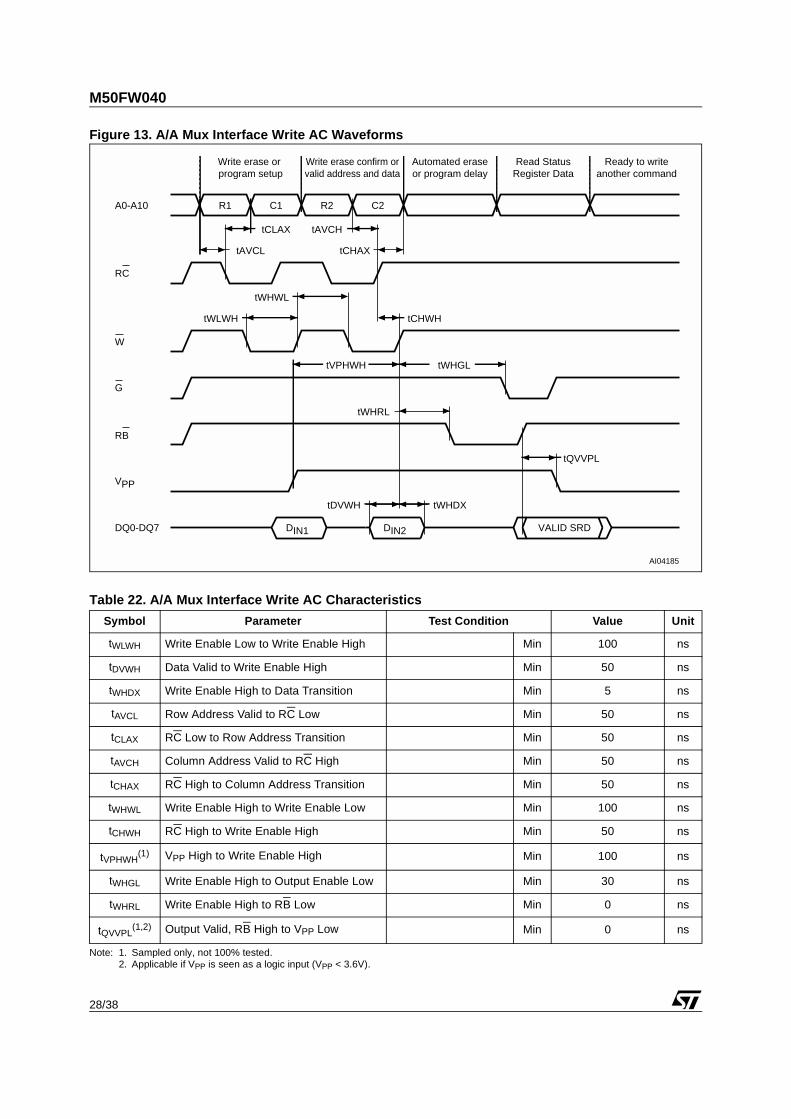
Figure 13. A/A Mux Interface Write AC Waveforms
Table 22. A/A Mux Interface Write AC Characteristics
Note: 1. Sampled only, not 100% tested.2. Applicable if VPP is seen as a logic input (VPP < 3.6V).
Symbol Parameter Test Condition Value Unit
tWLWH Write Enable Low to Write Enable High Min 100 ns
tDVWH Data Valid to Write Enable High Min 50 ns
tWHDX Write Enable High to Data Transition Min 5 ns
tAVCL Row Address Valid to RC Low Min 50 ns
tCLAX RC Low to Row Address Transition Min 50 ns
tAVCH Column Address Valid to RC High Min 50 ns
tCHAX RC High to Column Address Transition Min 50 ns
tWHWL Write Enable High to Write Enable Low Min 100 ns
tCHWH RC High to Write Enable High Min 50 ns
tVPHWH(1) VPP High to Write Enable High Min 100 ns
tWHGL Write Enable High to Output Enable Low Min 30 ns
tWHRL Write Enable High to RB Low Min 0 ns
tQVVPL(1,2) Output Valid, RB High to VPP Low Min 0 ns
AI04185
tCLAX
tCHAX
tWHDXtDVWH
VALID SRD
A0-A10
G
DQ0-DQ7
RC
tCHWH
tWHRL
C1
W
R1
tAVCL
tAVCH
R2 C2
tWLWH
tWHWL
RB
VPP
tVPHWH tWHGL
tQVVPL
DIN1 DIN2
Write erase or program setup
Write erase confirm orvalid address and data
Automated eraseor program delay
Read StatusRegister Data
Ready to writeanother command

29/38
M50FW040
PACKAGE MECHANICAL
Figure 14. PLCC32 – 32 pin Rectangular Plastic Leaded Chip Carrier, Package Outline
Note: Drawing is not to scale.
PLCC-A
D
E3 E1 E
1 N
D1
D3
CP
B
E2
e
B1
A1
A
R
0.51 (.020)
1.14 (.045)
F
A2
E2
D2 D2

M50FW040
30/38
Table 23. PLCC32 – 32 pin Rectangular Plastic Leaded Chip Carrier, Package Mechanical Data
Symbolmillimeters inches
Typ Min Max Typ Min Max
A 3.18 3.56 0.125 0.140
A1 1.53 2.41 0.060 0.095
A2 0.38 – 0.015 –
B 0.33 0.53 0.013 0.021
B1 0.66 0.81 0.026 0.032
CP 0.10 0.004
D 12.32 12.57 0.485 0.495
D1 11.35 11.51 0.447 0.453
D2 4.78 5.66 0.188 0.223
D3 7.62 – – 0.300 – –
E 14.86 15.11 0.585 0.595
E1 13.89 14.05 0.547 0.553
E2 6.05 6.93 0.238 0.273
E3 10.16 – – 0.400 – –
e 1.27 – – 0.050 – –
F 0.00 0.13 0.000 0.005
R 0.89 – – 0.035 – –
N 32 32

31/38
M50FW040
Figure 15. TSOP40 – 40 lead Plastic Thin Small Outline, 10x20 mm, Package Outline
Note: Drawing is not to scale.
Table 24. TSOP40 – 40 lead Plastic Thin Small Outline, 10x20 mm, Package Mechanical Data
Symbolmillimeters inches
Typ Min Max Typ Min Max
A 1.200 0.0472
A1 0.050 0.150 0.0020 0.0059
A2 0.950 1.050 0.0374 0.0413
B 0.170 0.270 0.0067 0.0106
C 0.100 0.210 0.0039 0.0083
CP 0.100 0.0039
D 19.800 20.200 0.7795 0.7953
D1 18.300 18.500 0.7205 0.7283
e 0.500 – – 0.0197 – –
E 9.900 10.100 0.3898 0.3976
L 0.500 0.700 0.0197 0.0276
α 0° 5° 0° 5°
N 40 40
TSOP-a
D1
E
1 N
CP
B
e
A2
A
N/2
D
DIE
C
LA1 α

M50FW040
32/38
PART NUMBERING
Table 25. Ordering Information Scheme
Devices are shipped from the factory with the memory content bits erased to ’1’.For a list of available options (Speed, Package, etc.) or for further information on any aspect of this device,please contact the ST Sales Office nearest to you.
Example: M50FW040 K 1 T G
Device TypeM50
ArchitectureF = Firmware Hub Interface
Operating VoltageW = 3V to 3.6V
Device Function040 = 4 Mbit (x8), Uniform Block
PackageK = PLCC32N = TSOP40: 10 x 20 mm
Device Grade5 = Temperature range –20 to 85 °C.Device tested with standard test flow1 = Temperature range 0 to 70 °C.Device tested with standard test flow
Optionblank = Standard PackingT = Tape & Reel Packing
Plating Technologyblank = Standard SnPb platingG = Lead-Free, RoHS compliant, Sb2O3-free and TBBA-free

33/38
M50FW040
FLOWCHARTS AND PSEUDO CODES
Figure 16. Program Flowchart and Pseudo Code
Note: 1. A Status check of b1 (Protected Block), b3 (VPP invalid) and b4 (Program Error) can be made after each Program operation byfollowing the correct command sequence.
2. If an error is found, the Status Register must be cleared before further Program/Erase Controller operations.
Write 40h or 10h
AI03407
Start
Write Address& Data
Read Status Register
YES
NOb7 = 1
YES
NOb3 = 0
NOb4 = 0
VPP InvalidError (1, 2)
ProgramError (1, 2)
Program command:– write 40h or 10h– write Address & Data (memory enters read status state after the Program command)
do:–read Status Register if Program/Erase Suspend command given execute suspend program loop
while b7 = 1
If b3 = 1, VPP invalid error:– error handler
If b4 = 1, Program error:– error handler
YES
End
YES
NOb1 = 0
Program to ProtectedBlock Error (1, 2)
If b1 = 1, Program to protected block error:– error handler
Suspend
SuspendLoop
NO
YES
FWHInterface
Only

M50FW040
34/38
Figure 17. Program Suspend & Resume Flowchart and Pseudo Code
Write 70h
AI03408
Read Status Register
YES
NOb7 = 1
YES
NOb2 = 1
Program Continues
Write a readCommand
Program/Erase Suspend command:– write B0h– write 70h
do:– read Status Register
while b7 = 1
If b2 = 0 Program completed
Write D0hProgram/Erase Resume command:– write D0h to resume the program– if the Program operation completed then this is not necessary. The device returns to Read as normal (as if the Program/Erase suspend was not issued).
Read data fromanother address
Start
Write B0h
Program Complete
Write FFh
Read Data
35/38
M50FW040
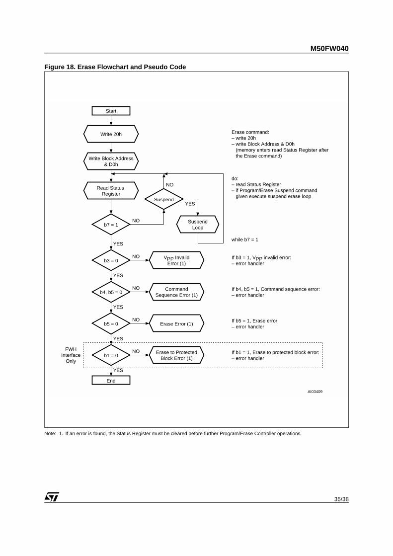
Figure 18. Erase Flowchart and Pseudo Code
Note: 1. If an error is found, the Status Register must be cleared before further Program/Erase Controller operations.
Write 20h
AI03409
Start
Write Block Address& D0h
Read Status Register
YES
NOb7 = 1
YES
NOb3 = 0
NOb4, b5 = 0
VPP InvalidError (1)
CommandSequence Error (1)
Erase command:– write 20h– write Block Address & D0h (memory enters read Status Register after the Erase command)
do:– read Status Register– if Program/Erase Suspend command given execute suspend erase loop
while b7 = 1
If b3 = 1, VPP invalid error:– error handler
If b4, b5 = 1, Command sequence error:– error handler
YES
NOb5 = 0 Erase Error (1)
YES
NO
Suspend
SuspendLoop
If b5 = 1, Erase error:– error handler
End
YES
NOb1 = 0
Erase to ProtectedBlock Error (1)
If b1 = 1, Erase to protected block error:– error handler
YES
FWHInterface
Only

M50FW040
36/38
Figure 19. Erase Suspend & Resume Flowchart and Pseudo Code
Write 70h
AI03410
Read Status Register
YES
NOb7 = 1
YES
NOb6 = 1
Erase Continues
Program/Erase Suspend command:– write B0h– write 70h
do:– read Status Register
while b7 = 1
If b6 = 0, Erase completed
Write D0h
Read data fromanother block
orProgram
Start
Write B0h
Erase Complete
Write FFh
Read Data
Program/Erase Resume command:– write D0h to resume erase– if the Erase operation completed then this is not necessary. The device returns to Read as normal (as if the Program/Erase suspend was not issued).

37/38
M50FW040
REVISION HISTORY
Table 26. Document Revision History
Date Version Revision Details
September 2000 -01 First Issue
04-Oct-2000 -02 DC Characteristics: ICC4 changed
11-Apr-01 -03 Document type: from Preliminary Data to Data SheetProgram and Erase functions clarificationRead Electronic Signature table changeFWH Register Configuration Map table changeInput Register Definition table, note clarificationDC Characteristics parameters clarification and new VIH and VIL parameters addedFWH Interface AC Signal Timing Characteristics changeA/A Mux Interface Read AC Characteristics changeA/A Mux Interface Write AC Characteristics changeA/A Mux Interface Write AC Waveforms change
06-Jul-2001 -04 Note 2 changed (Table 12., Absolute Maximum Ratings)
12-Mar-2002 -05RFU pins must be left disconnectedSpecification of PLCC32 package mechanical data revised
09-Jul-2004 6.0
Revision numbering modified.Document imported in new template (and so reformatted).Temperature Range ordering information replaced by Device Grade, Standard packing option added and Plating Technology added to Table 25., Ordering Information Scheme. TLEAD parameter added to Table 12., Absolute Maximum Ratings and TBIAS parameter removed.
12-Jul-2001 7.0 Inches values corrected in Table 25., Ordering Information Scheme.

M50FW040
38/38
Information furnished is believed to be accurate and reliable. However, STMicroelectronics assumes no responsibility for the consequences of use of such information nor for any infringement of patents or other rights of third parties which may result from its use. No license is granted by implication or otherwise under any patent or patent rights of STMicroelectronics. Specifications mentioned in this publication are subject to change without notice. This publication supersedes and replaces all information previously supplied. STMicroelectronics products are not
authorized for use as critical components in life support devices or systems without express written approval of STMicroelectronics.
The ST logo is a registered trademark of STMicroelectronics.
All other names are the property of their respective owners.
© 2004 STMicroelectronics - All rights reserved
STMicroelectronics GROUP OF COMPANIESAustralia - Belgium - Brazil - Canada - China - Czech Republic - Finland - France - Germany -
Hong Kong - India - Israel - Italy - Japan - Malaysia - Malta - Morocco - Singapore -Spain - Sweden - Switzerland - United Kingdom - United States
www.st.com