Embed Size (px)
Citation preview
®
Using ProgrammableI/O Standards
in Mercury DevicesMay 2003, ver. 2.2 Application Note 134
Introduction Programmable logic devices (PLDs) use I/O standards to interface with memory, microprocessors, backplanes, and peripheral devices. Designers who want to use these standards with programmable logic need flexible, high-performance, multi-standard I/O buffers. PLD support for industry I/O standards improves designers’ time-to-market.
Programmable I/O standards simplify board design. Integrating dedicated circuitry such as translation buffers, LVDS, LVPECL, and clock data recovery (CDR) into PLDs saves board space, reduces pin usage, and improves performance. Altera’s MercuryTM devices offer the highest-performance programmable logic solution with the I/O standards necessary for the communication and computer industries.
A single Mercury device can simultaneously support multiple I/O standards, as well as interface with high-speed, low-voltage memory buses and backplanes. Mercury devices feature source-synchronous-signalling and CDR circuitry that supports data rates up to 1.25 gigabits per second (Gbps).
This application note provides guidelines for designing with programmable I/O standards in Mercury devices and covers the following topics:
I/O Standards Mercury I/O Banks Operating Conditions Board Termination Schemes Guidelines for Programmable I/O Standards Software Support
I/O Standards This section provides an overview of typical applications for the programmable I/O standards supported by Mercury devices. The specifications for each I/O standard are also listed.
The Mercury I/O buffers meet the voltage, drive strength, and AC characteristics necessary to comply with the I/O standards listed in Table 1.
Altera Corporation 1
AN-134-2.2
AN 134: Using Programmable I/O Standards in Mercury Devices
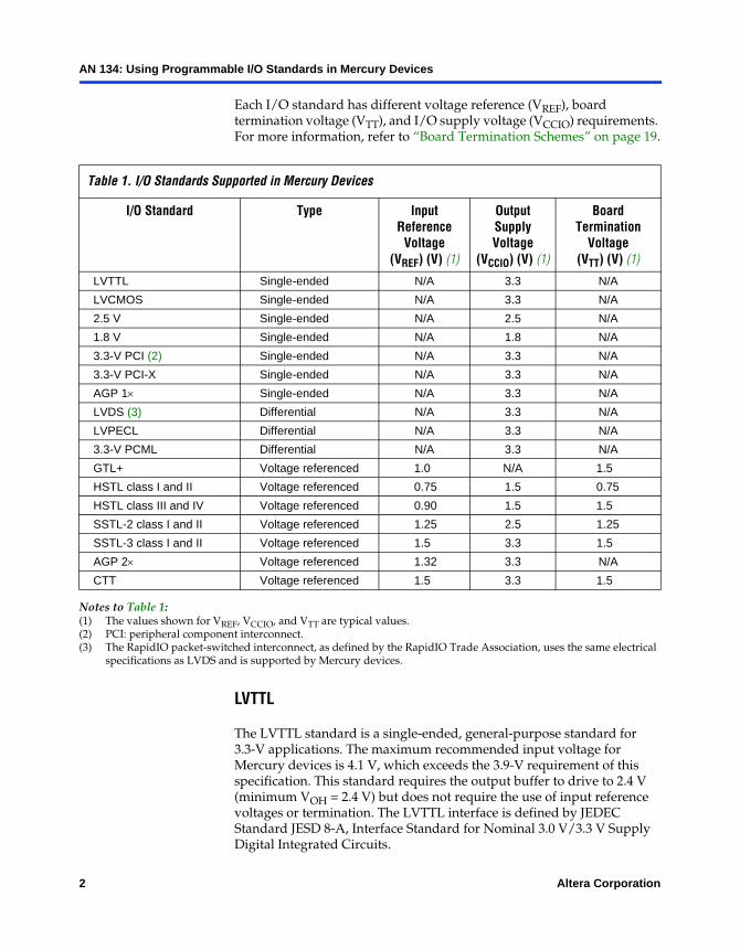
Each I/O standard has different voltage reference (VREF), board termination voltage (VTT), and I/O supply voltage (VCCIO) requirements. For more information, refer to “Board Termination Schemes” on page 19.
Notes to Table 1:(1) The values shown for VREF, VCCIO, and VTT are typical values.(2) PCI: peripheral component interconnect.(3) The RapidIO packet-switched interconnect, as defined by the RapidIO Trade Association, uses the same electrical
specifications as LVDS and is supported by Mercury devices.
LVTTL
The LVTTL standard is a single-ended, general-purpose standard for 3.3-V applications. The maximum recommended input voltage for Mercury devices is 4.1 V, which exceeds the 3.9-V requirement of this specification. This standard requires the output buffer to drive to 2.4 V (minimum VOH = 2.4 V) but does not require the use of input reference voltages or termination. The LVTTL interface is defined by JEDEC Standard JESD 8-A, Interface Standard for Nominal 3.0 V/3.3 V Supply Digital Integrated Circuits.
Table 1. I/O Standards Supported in Mercury Devices
I/O Standard Type Input Reference
Voltage (VREF) (V) (1)
OutputSupplyVoltage
(VCCIO) (V) (1)
Board Termination
Voltage(VTT) (V) (1)
LVTTL Single-ended N/A 3.3 N/A
LVCMOS Single-ended N/A 3.3 N/A
2.5 V Single-ended N/A 2.5 N/A
1.8 V Single-ended N/A 1.8 N/A
3.3-V PCI (2) Single-ended N/A 3.3 N/A
3.3-V PCI-X Single-ended N/A 3.3 N/A
AGP 1× Single-ended N/A 3.3 N/A
LVDS (3) Differential N/A 3.3 N/A
LVPECL Differential N/A 3.3 N/A
3.3-V PCML Differential N/A 3.3 N/A
GTL+ Voltage referenced 1.0 N/A 1.5
HSTL class I and II Voltage referenced 0.75 1.5 0.75
HSTL class III and IV Voltage referenced 0.90 1.5 1.5
SSTL-2 class I and II Voltage referenced 1.25 2.5 1.25
SSTL-3 class I and II Voltage referenced 1.5 3.3 1.5
AGP 2× Voltage referenced 1.32 3.3 N/A
CTT Voltage referenced 1.5 3.3 1.5
2 Altera Corporation
AN 134: Using Programmable I/O Standards in Mercury Devices
LVCMOS
LVCMOS is a single-ended general-purpose standard used for 3.3-V applications. The input buffer requirements are the same as the LVTTL requirements, and the output buffer is required to drive to the rail (minimum VOH = VCCIO – 0.2 V). This standard requires a 3.3-V I/O supply voltage (VCCIO), but not the use of input reference voltages or termination. The LVCMOS standard is defined in JEDEC Standard JESD 8-A, Interface Standard for Nominal 3.0 V/3.3 V Supply Digital Integrated Circuits.
2.5 V
The 2.5-V standard is similar to LVCMOS but is used for 2.5-V power supply levels. Mercury devices meet the normal range of this specification. This standard requires a 2.5-V VCCIO, but not the use of input reference voltages or termination. The 2.5-V I/O standard is documented by JEDEC Standard JESD 8-5, 2.5 V ±0.2 V (Normal Range) and 1.7 V to 2.7 V (Wide Range) Power Supply Voltage and Interface Standard for Nonterminated Digital Integrated Circuit.
1.8 V
The 1.8-V I/O standard is similar to LVCMOS but is used for 1.8-V power supply levels and reduced input and output thresholds. Mercury devices meet the normal range of this specification. This standard requires a 1.8-V VCCIO, but not the use of input reference voltages or termination. The 1.8-V I/O standard is documented by JEDEC Standard JESD 8-7, 1.8 V ±0.15 V (Normal Range) and 1.2 V to 1.95 V (Wide Range) Power Supply Voltage and Interface Standard for Nonterminated Digital Integrated Circuit.
3.3-V PCI
Mercury devices are compliant with PCI Local Bus Specification, Revision 2.2 for 3.3-V operation. At 3.3 V, the PCI standard supports up to 64-bit bus width operation at 33 or 66 MHz. This standard uses LVTTL-type input and output buffers and requires a 3.3-V VCCIO, but not the use of input reference voltages or termination.
Altera Corporation 3
AN 134: Using Programmable I/O Standards in Mercury Devices
PCI-X
An enhanced version of the PCI specification that can support higher average bandwidth, PCI-X has more stringent requirements than PCI. PCI-X provides backward compatibility by allowing devices to operate at conventional PCI frequencies (33 MHz and 66 MHz).
LVDS
The LVDS I/O standard is used for very high-performance, low-power-consumption data transfer. Two key industry standards define LVDS: IEEE 1596.3 SCI-LVDS and ANSI/TIA/EIA-644. Both standards have similar key features, but the IEEE standard supports a maximum data transfer of 250 megabits per second (Mbps). Mercury devices are designed to meet the ANSI/TIA/EIA-644 requirements at up to 840 Mbps using source synchronous mode, and up to 1.25 Gbps in CDR mode. The LVDS standard requires a 3.3-V VCCIO and a 100-Ω termination resistor between the two traces at the input buffer. No input reference voltage is required.
LVPECL
The LVPECL standard is used in video graphic, telecommunications, and data communication designs. It is also used for clock distribution. LVPECL is a differential I/O standard that is similar to LVDS, but with a different common mode and differential voltage. The LVPECL standard requires a 3.3-V VCCIO and a 100-Ω termination resistor between the two traces at the input buffer. No input reference voltage is required.
3.3-V PCML
3.3-V PCML is a differential standard used for high-speed interfacing. 3.3-V PCML requires a 3.3-V VCCIO and a 100-Ω termination resistor between the two traces at the input buffer. In addition, each input trace requires a 50-Ω resistor to VTT, and each output trace requires a 100-Ω resistor to VTT. No input reference voltage is required.
f For more information on CDR mode, refer to Application Note 130 (CDR in Mercury Devices).
4 Altera Corporation
AN 134: Using Programmable I/O Standards in Mercury Devices
GTL+
The GTL+ standard is a high-speed bus standard first used by Intel Corporation for interfacing with the Pentium Pro processor. GTL+ is a voltage-referenced standard requiring a 1.0-V input VREF and a 1.5-V VTT. Because GTL+ is an open-drain standard, it does not require a particular VCCIO supply voltage. GTL+ is often used for processor interfacing or communication across a backplane.
HSTL Class I, II, III & IV
The HSTL standard is a 1.5-V output buffer supply voltage-based interface standard for digital integrated circuits. HSTL is a voltage-referenced standard requiring a 0.75-V VREF, a 1.5-V VCCIO, and a 0.75-V VTT. HSTL class III and IV require a 0.9-V VREF, a 1.5-V VCCIO, and a 1.5-V VTT.The HSTL standard is specified by JEDEC Standard JESD 8-6, High-Speed Transceiver Logic (HSTL).
SSTL-2 Class I & II
The SSTL-2 standard is a voltage-referenced standard requiring a 1.125-V VREF, a 2.5-V VCCIO, and a 1.125-V VTT. SSTL-2 is used for high-speed SDRAM interfaces. The SSTL-2 I/O standard is specified by JEDEC Standard JESD 8-9, Stub-Series Terminated Logic for 2.5 Volts (SSTL-2).
SSTL-3 Class I & II
The SSTL-3 standard is a voltage-referenced standard requiring a 1.5-V VREF, a 3.3-V VCCIO, and a 1.5-V VTT. SSTL-3 is used for high-speed SDRAM interfaces. The SSTL-3 I/O standard is specified by JEDEC Standard JESD 8-8, Stub-Series Terminated Logic for 3.3 Volts (SSTL-3).
AGP
Mercury devices support the AGP interface in both 1× and 2× modes. AGP 2× is a voltage-referenced standard requiring a 1.32-V VREF, and a 3.3-V VCCIO. This I/O standard does not require termination. The AGP standard is specified by the Advanced Graphics Port Interface Specification Revision 2.0 introduced by Intel Corporation for graphics applications.
Altera Corporation 5
AN 134: Using Programmable I/O Standards in Mercury Devices
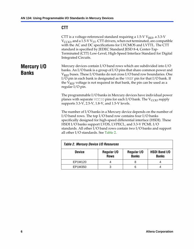
CTT
CTT is a voltage-referenced standard requiring a 1.5-V VREF, a 3.3-V VCCIO, and a 1.5-V VTT. CTT drivers, when not terminated, are compatible with the AC and DC specifications for LVCMOS and LVTTL. The CTT standard is specified by JEDEC Standard JESD 8-4, Center-Tap-Terminated (CTT) Low-Level, High-Speed Interface Standard for Digital Integrated Circuits.
Mercury I/O Banks
Mercury devices contain I/O band rows which are subdivided into I/O banks. An I/O bank is a group of I/O pins that share common power and VREF buses. These I/O banks do not cross I/O band row boundaries. One I/O pin in each bank is designated as the VREF pin for that I/O bank. If the VREF voltage is not required in that bank, the pin can be used as a regular I/O pin.
The programmable I/O banks in Mercury devices have individual power planes with separate VCCIO pins for each I/O bank. The VCCIO supply supports 3.3-V, 2.5-V, 1.8-V, and 1.5-V levels.
The number of I/O banks in a Mercury device depends on the number of I/O band rows. The top I/O band row contains four I/O banks specifically designed for high-speed differential interface (HSDI). These HSDI I/O banks support LVDS, LVPECL, and 3.3-V PCML I/O standards. All other I/O band rows contain two I/O banks and support all other I/O standards. See Table 2.
Table 2. Mercury Device I/O Resources
Device Regular I/O Rows
Regular I/O Banks
HSDI Band I/O Banks
EP1M120 4 8 4
EP1M350 3 6 4
6 Altera Corporation
AN 134: Using Programmable I/O Standards in Mercury Devices
The HSDI I/O banks can operate in source synchronous or CDR modes. When used as regular I/O banks, the HSDI transmitter banks support all the I/O standards shown in Table 1. The HSDI receiver banks support the I/O output standards and drive strengths, as shown in Table 3.
The following is a list of HSDI receiver I/O banks input standards:
LVCMOS LVTTL (3.3 V) LVTTL (2.5 V) LVTTL (1.8 V) GTL+ (3.3 V) HSTL Class I and II SSTL-3 Class I and II SSTL-2 Class I and II
The top I/O banks 1, 2, 3, and 4 only support non-HSDI I/O pins if HSDI circuitry is unused. If any HSDI channel is used, banks 1, 2, 3, and 4, do not support regular I/O pins. For more information on CDR mode, refer to Application Note 130 (CDR in Mercury Devices).
Table 3. HDSI Receiver I/O Banks Output Standard & Drive Strength Support
Output Standard Drive Strength
LVTTL (3.3 V) 4 mA
8 mA
12 mA
16 mA
24 mA
LVTTL (2.5 V) 4 mA
8 mA
12 mA
16 mA
LVTTL (1.8 V) 2 mA
4 mA
STTL-3 Class I and II Minimum
Maximum
STTL-2 Class I and II Minimum
Altera Corporation 7
AN 134: Using Programmable I/O Standards in Mercury Devices
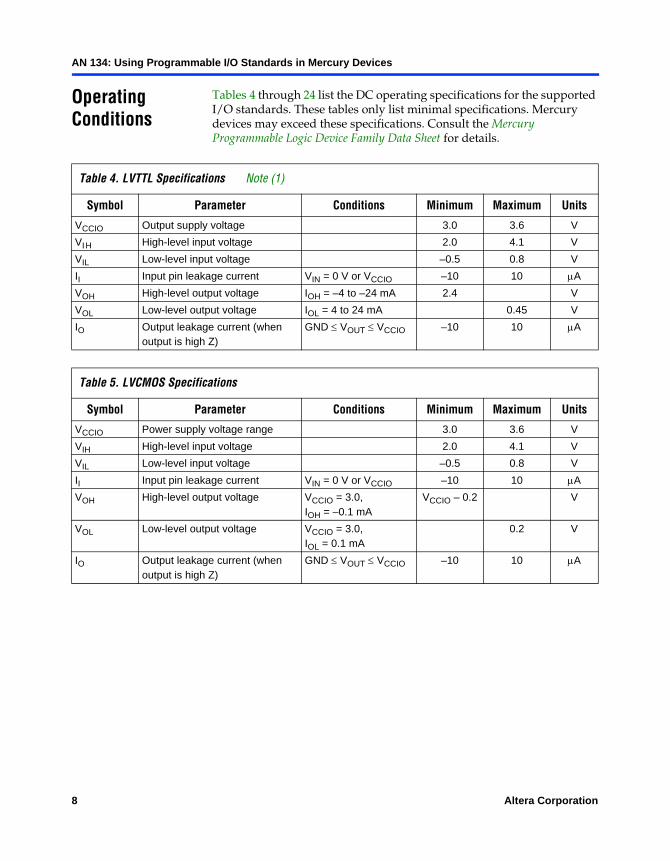
Operating Conditions
Tables 4 through 24 list the DC operating specifications for the supported I/O standards. These tables only list minimal specifications. Mercury devices may exceed these specifications. Consult the Mercury Programmable Logic Device Family Data Sheet for details.
Table 4. LVTTL Specifications Note (1)
Symbol Parameter Conditions Minimum Maximum Units
VCCIO Output supply voltage 3.0 3.6 V
VIH High-level input voltage 2.0 4.1 V
VIL Low-level input voltage –0.5 0.8 V
II Input pin leakage current VIN = 0 V or VCCIO –10 10 µA
VOH High-level output voltage IOH = –4 to –24 mA 2.4 V
VOL Low-level output voltage IOL = 4 to 24 mA 0.45 V
IO Output leakage current (when output is high Z)
GND ≤ VOUT ≤ VCCIO –10 10 µA
Table 5. LVCMOS Specifications
Symbol Parameter Conditions Minimum Maximum Units
VCCIO Power supply voltage range 3.0 3.6 V
VIH High-level input voltage 2.0 4.1 V
VIL Low-level input voltage –0.5 0.8 V
II Input pin leakage current VIN = 0 V or VCCIO –10 10 µA
VOH High-level output voltage VCCIO = 3.0, IOH = –0.1 mA
VCCIO – 0.2 V
VOL Low-level output voltage VCCIO = 3.0,IOL = 0.1 mA
0.2 V
IO Output leakage current (when output is high Z)
GND ≤ VOUT ≤ VCCIO –10 10 µA
8 Altera Corporation
AN 134: Using Programmable I/O Standards in Mercury Devices
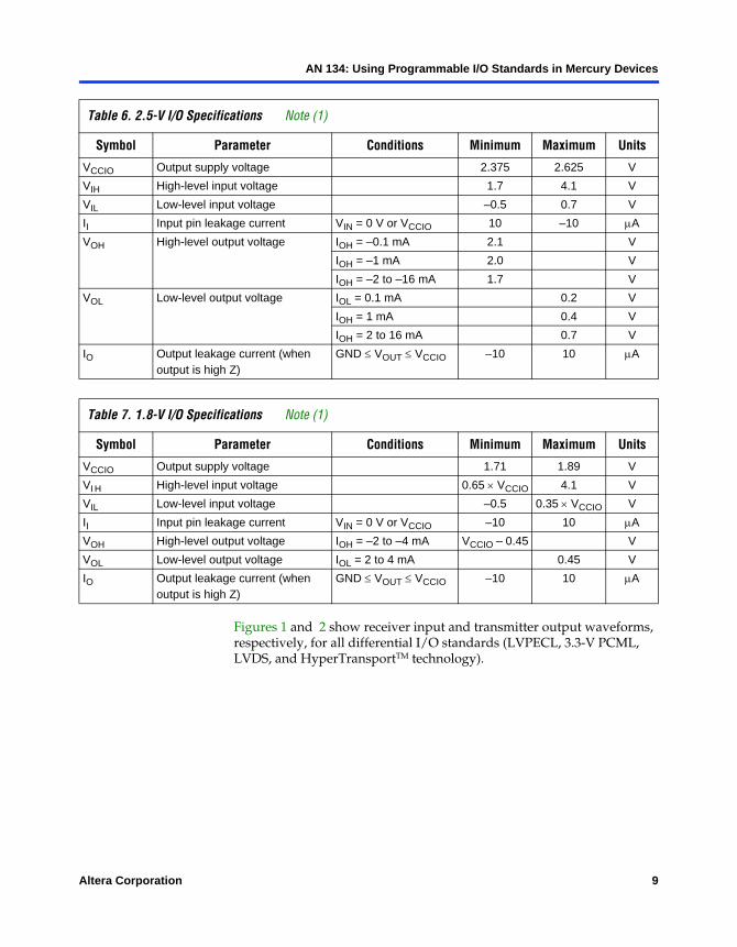
Figures 1 and 2 show receiver input and transmitter output waveforms, respectively, for all differential I/O standards (LVPECL, 3.3-V PCML, LVDS, and HyperTransportTM technology).
Table 6. 2.5-V I/O Specifications Note (1)
Symbol Parameter Conditions Minimum Maximum Units
VCCIO Output supply voltage 2.375 2.625 V
VIH High-level input voltage 1.7 4.1 V
VIL Low-level input voltage –0.5 0.7 V
II Input pin leakage current VIN = 0 V or VCCIO 10 –10 µA
VOH High-level output voltage IOH = –0.1 mA 2.1 V
IOH = –1 mA 2.0 V
IOH = –2 to –16 mA 1.7 V
VOL Low-level output voltage IOL = 0.1 mA 0.2 V
IOH = 1 mA 0.4 V
IOH = 2 to 16 mA 0.7 V
IO Output leakage current (when output is high Z)
GND ≤ VOUT ≤ VCCIO –10 10 µA
Table 7. 1.8-V I/O Specifications Note (1)
Symbol Parameter Conditions Minimum Maximum Units
VCCIO Output supply voltage 1.71 1.89 V
VI H High-level input voltage 0.65 × VCCIO 4.1 V
VIL Low-level input voltage –0.5 0.35 × VCCIO V
II Input pin leakage current VIN = 0 V or VCCIO –10 10 µA
VOH High-level output voltage IOH = –2 to –4 mA VCCIO – 0.45 V
VOL Low-level output voltage IOL = 2 to 4 mA 0.45 V
IO Output leakage current (when output is high Z)
GND ≤ VOUT ≤ VCCIO –10 10 µA
Altera Corporation 9
AN 134: Using Programmable I/O Standards in Mercury Devices
Figure 1. Receiver Input Waveforms for Differential I/O Standards
Figure 2. Transmitter Output Waveforms for Differential I/O Standards
Single-Ended Waveform
Differential Waveform
Positive Channel (p) = VIH
Negative Channel (n) = VIL
Ground
±VID
+VID
− VIDVID (Peak-to-Peak)
VCM
p − n = 0 V
Single-Ended Waveform
Differential Waveform
Positive Channel (p) = VOH
Negative Channel (n) = VOL
Ground
±VOD
+VOD
− VODVOD (Peak-to-Peak)
p − n = 0 V
VCM
10 Altera Corporation
AN 134: Using Programmable I/O Standards in Mercury Devices
Transmitter Output Waveforms for Differential I/O Standards
Table 8. 3.3-V LVDS I/O Specifications Note (2)
Symbol Parameter Conditions Minimum Typical Maximum Units
VCCIO I/O supply voltage 3.135 3.3 3.465 V
VOD Differential output voltage RL = 100 Ω 250 450 mV
∆ VOD Change in VOD between high and low
RL = 100 Ω 50 mV
VOS Output offset voltage RL = 100 Ω 1.125 1.25 1.375 V
∆ VOS Change in VOS between high and low
RL = 100 Ω 50 mV
VTH Differential input threshold VCM = 1.2 V (6) –100 100 mV
VIN Receiver input voltage range
0.0 2.4 V
RL Receiver differential input resistor (external to Mercury devices)
90 100 110 Ω
Table 9. LVPECL Specifications
Symbol Parameter Conditions Minimum Typical Maximum Units
VCCIO I/O supply voltage 3.135 3.3 3.465 V
VIL Low-level input voltage 0 2,000 mV
VIH High-level input voltage 400 2,470 mV
VOL Low-level output voltage 1,400 1,650 mV
VOH High-level output voltage 2,275 2,470 mV
VID Differential input voltage (3)
400 600 1,200 mV
VOD Differential output voltage (3)
525 1,050 1,200 mV
tR Rise time (20 to 80%) (4) 85 325 ps
tF Fall time (20 to 80%) (4) 85 325 ps
tDSKEW Differential skew 25 ps
RL Receiver differential input resistor
100 Ω
Altera Corporation 11
AN 134: Using Programmable I/O Standards in Mercury Devices
Table 10. 3.3-V PCML Specifications
Symbol Parameter Conditions Minimum Typical Maximum Units
VCCIO I/O supply voltage 3.135 3.3 3.465 V
VIL Low-level input voltage VCCIO – 0.3
V
VIH High-level input voltage VCCIO V
VOL Low-level output voltage VCCIO – 0.6
VCCIO – 0.3
V
VOH High-level output voltage VCCIO VCCIO – 0.3
V
VT Output termination voltage VCCIO V
VOD Differential output voltage 300 450 600 mV
tR Rise time (20 to 80%) 200 ps
tF Fall time (20 to 80%) 200 ps
tDSKEW Differential skew 25 ps
RO Output load 100 Ω
RL Receiver differential input resistor
45 50 55 Ω
Table 11. 3.3-V PCI Specifications
Symbol Parameter Conditions Minimum Typical Maximum Units
VCCIO I/O supply voltage 3.0 3.3 3.6 V
VIH High-level input voltage 0.5 × VCCIO
VCCIO + 0.5
V
VIL Low-level input voltage –0.5 0.3 × VCCIO
V
II Input pin leakage current 0 < VIN < VCCIO –10 10 µA
VOH High-level output voltage IOUT = –500 µA 0.9 × VCCIO
V
VOL Low-level output voltage IOUT = 1,500 µA 0.1 × VCCIO
V
IO Output leakage current (when output is high Z)
GND ≤ VOUT ≤ VCCIO –10 10 µA
12 Altera Corporation
AN 134: Using Programmable I/O Standards in Mercury Devices
Table 12. PCI-X Specifications
Symbol Parameter Conditions Minimum Typical Maximum Units
VCCIO I/O supply voltage 3.0 3.6 V
VIH High-level input voltage 0.5 × VCCIO
VCCIO + 0.5
V
VIL Low-level input voltage –0.5 0.35 × VCCIO
V
VIPU Input pull-up voltage 0.7 × VCCIO
V
II Input leakage current 0 < VIN < VCCIO –10 10 µA
VOH High-level output voltage IOUT = –500 µA 0.9 × VCCIO
V
VOL Low-level output voltage IOUT = 1,500 µA 0.1 × VCCIO
V
IO Output leakage current (when output is high Z)
GND ≤ VOUT ≤ VCCIO –10 10 µA
LPIN Pin inductance 15 nH
Table 13. GTL+ I/O Specifications Note (1)
Symbol Parameter Conditions Minimum Typical Maximum Units
VTT Termination voltage 1.35 1.5 1.65 V
VREF Reference voltage 0.88 1.0 1.12 V
VIH High-level input voltage VREF + 0.1 V
VIL Low-level input voltage VREF – 0.1 V
II Input leakage current 0 < VIN < VCCIO –10 10 µA
VOL Low-level output voltage IOL = 34 to 46 mA 0.65 V
IO Output leakage current (when output is high Z)
GND ≤ VOUT ≤ VCCIO –10 10 µA
Altera Corporation 13
AN 134: Using Programmable I/O Standards in Mercury Devices
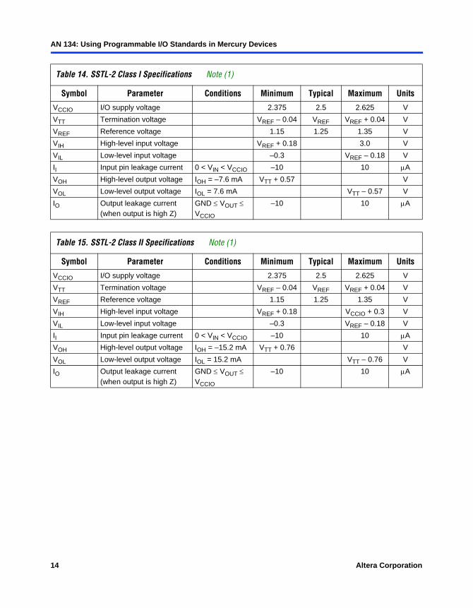
Table 14. SSTL-2 Class I Specifications Note (1)
Symbol Parameter Conditions Minimum Typical Maximum Units
VCCIO I/O supply voltage 2.375 2.5 2.625 V
VTT Termination voltage VREF – 0.04 VREF VREF + 0.04 V
VREF Reference voltage 1.15 1.25 1.35 V
VIH High-level input voltage VREF + 0.18 3.0 V
VIL Low-level input voltage –0.3 VREF – 0.18 V
II Input pin leakage current 0 < VIN < VCCIO –10 10 µA
VOH High-level output voltage IOH = –7.6 mA VTT + 0.57 V
VOL Low-level output voltage IOL = 7.6 mA VTT – 0.57 V
IO Output leakage current (when output is high Z)
GND ≤ VOUT ≤ VCCIO
–10 10 µA
Table 15. SSTL-2 Class II Specifications Note (1)
Symbol Parameter Conditions Minimum Typical Maximum Units
VCCIO I/O supply voltage 2.375 2.5 2.625 V
VTT Termination voltage VREF – 0.04 VREF VREF + 0.04 V
VREF Reference voltage 1.15 1.25 1.35 V
VIH High-level input voltage VREF + 0.18 VCCIO + 0.3 V
VIL Low-level input voltage –0.3 VREF – 0.18 V
II Input pin leakage current 0 < VIN < VCCIO –10 10 µA
VOH High-level output voltage IOH = –15.2 mA VTT + 0.76 V
VOL Low-level output voltage IOL = 15.2 mA VTT – 0.76 V
IO Output leakage current (when output is high Z)
GND ≤ VOUT ≤ VCCIO
–10 10 µA
14 Altera Corporation
AN 134: Using Programmable I/O Standards in Mercury Devices
Table 16. SSTL-3 Class I Specifications Note (1)
Symbol Parameter Conditions Minimum Typical Maximum Units
VCCIO I/O supply voltage 3.0 3.3 3.6 V
VTT Termination voltage VREF – 0.05 VREF VREF + 0.05 V
VREF Reference voltage 1.3 1.5 1.7 V
VIH High-level input voltage VREF + 0.2 VCCIO + 0.3 V
VIL Low-level input voltage –0.3 VREF – 0.2 V
II Input pin leakage current 0 < VIN < VCCIO –10 10 µA
VOH High-level output voltage IOH = –8 mA VTT + 0.6 V
VOL Low-level output voltage IOL = 8 mA VTT – 0.6 V
IO Output leakage current (when output is high Z)
GND ≤ VOUT ≤ VCCIO
–10 10 µA
Table 17. SSTL-3 Class II Specifications Note (1)
Symbol Parameter Conditions Minimum Typical Maximum Units
VCCIO I/O supply voltage 3.0 3.3 3.6 V
VTT Termination voltage VREF – 0.05 VREF VREF + 0.05 V
VREF Reference voltage 1.3 1.5 1.7 V
VIH High-level input voltage VREF + 0.2 VCCIO + 0.3 V
VIL Low-level input voltage –0.3 VREF – 0.2 V
II Input pin leakage current 0 < VIN < VCCIO –10 10 µA
VOH High-level output voltage IOH = –16 mA VT T + 0.8 V
VOL Low-level output voltage IOL = 16 mA VTT – 0.8 V
IO Output leakage current (when output is high Z)
GND ≤ VOUT ≤ VCCIO
–10 10 µA
Table 18. 3.3-V AGP 2× Specifications
Symbol Parameter Conditions Minimum Typical Maximum Units
VCCIO I/O supply voltage 3.15 3.3 3.45 V
VREF Reference voltage 0.39 × VCCIO 0.41 × VCCIO V
VIH High-level input voltage (5) 0.5 × VCCIO VCCIO + 0.5 V
VIL Low-level input voltage (5) 0.3 × VCCIO V
VOH High-level output voltage IOUT = –20 µA 0.9 × VCCIO 3.6 V
VOL Low-level output voltage IOUT = 20 µA 0.1 × VCCIO V
II Input pin leakage current 0 < VI N < VCCIO –10 10 µA
IO Output leakage current (when output is high Z)
GND ≤ VOUT ≤ VCCIO
–10 10 µA
Altera Corporation 15
AN 134: Using Programmable I/O Standards in Mercury Devices
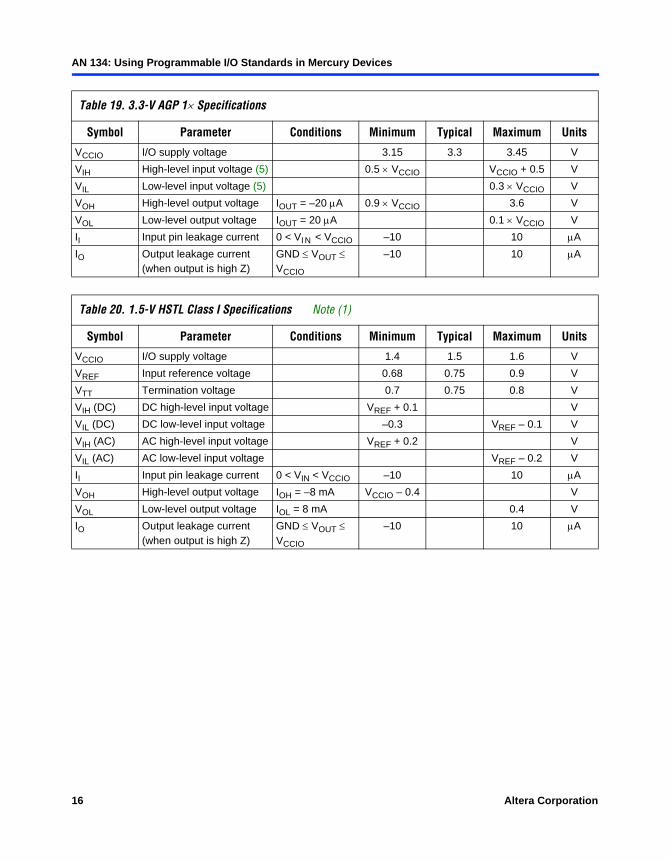
Table 19. 3.3-V AGP 1× Specifications
Symbol Parameter Conditions Minimum Typical Maximum Units
VCCIO I/O supply voltage 3.15 3.3 3.45 V
VIH High-level input voltage (5) 0.5 × VCCIO VCCIO + 0.5 V
VIL Low-level input voltage (5) 0.3 × VCCIO V
VOH High-level output voltage IOUT = –20 µA 0.9 × VCCIO 3.6 V
VOL Low-level output voltage IOUT = 20 µA 0.1 × VCCIO V
II Input pin leakage current 0 < VI N < VCCIO –10 10 µA
IO Output leakage current (when output is high Z)
GND ≤ VOUT ≤ VCCIO
–10 10 µA
Table 20. 1.5-V HSTL Class I Specifications Note (1)
Symbol Parameter Conditions Minimum Typical Maximum Units
VCCIO I/O supply voltage 1.4 1.5 1.6 V
VREF Input reference voltage 0.68 0.75 0.9 V
VTT Termination voltage 0.7 0.75 0.8 V
VIH (DC) DC high-level input voltage VREF + 0.1 V
VIL (DC) DC low-level input voltage –0.3 VREF – 0.1 V
VIH (AC) AC high-level input voltage VREF + 0.2 V
VIL (AC) AC low-level input voltage VREF – 0.2 V
II Input pin leakage current 0 < VIN < VCCIO –10 10 µA
VOH High-level output voltage IOH = –8 mA VCCIO – 0.4 V
VOL Low-level output voltage IOL = 8 mA 0.4 V
IO Output leakage current (when output is high Z)
GND ≤ VOUT ≤ VCCIO
–10 10 µA
16 Altera Corporation
AN 134: Using Programmable I/O Standards in Mercury Devices
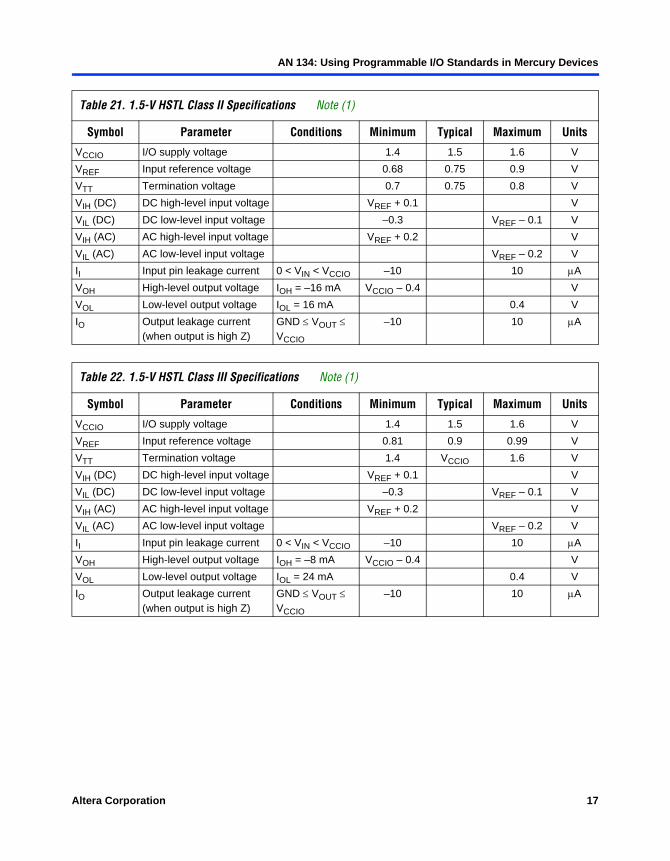
Table 21. 1.5-V HSTL Class II Specifications Note (1)
Symbol Parameter Conditions Minimum Typical Maximum Units
VCCIO I/O supply voltage 1.4 1.5 1.6 V
VREF Input reference voltage 0.68 0.75 0.9 V
VTT Termination voltage 0.7 0.75 0.8 V
VIH (DC) DC high-level input voltage VREF + 0.1 V
VIL (DC) DC low-level input voltage –0.3 VREF – 0.1 V
VIH (AC) AC high-level input voltage VREF + 0.2 V
VIL (AC) AC low-level input voltage VREF – 0.2 V
II Input pin leakage current 0 < VIN < VCCIO –10 10 µA
VOH High-level output voltage IOH = –16 mA VCCIO – 0.4 V
VOL Low-level output voltage IOL = 16 mA 0.4 V
IO Output leakage current (when output is high Z)
GND ≤ VOUT ≤ VCCIO
–10 10 µA
Table 22. 1.5-V HSTL Class III Specifications Note (1)
Symbol Parameter Conditions Minimum Typical Maximum Units
VCCIO I/O supply voltage 1.4 1.5 1.6 V
VREF Input reference voltage 0.81 0.9 0.99 V
VTT Termination voltage 1.4 VCCIO 1.6 V
VIH (DC) DC high-level input voltage VREF + 0.1 V
VIL (DC) DC low-level input voltage –0.3 VREF – 0.1 V
VIH (AC) AC high-level input voltage VREF + 0.2 V
VIL (AC) AC low-level input voltage VREF – 0.2 V
II Input pin leakage current 0 < VIN < VCCIO –10 10 µA
VOH High-level output voltage IOH = –8 mA VCCIO – 0.4 V
VOL Low-level output voltage IOL = 24 mA 0.4 V
IO Output leakage current (when output is high Z)
GND ≤ VOUT ≤ VCCIO
–10 10 µA
Altera Corporation 17
AN 134: Using Programmable I/O Standards in Mercury Devices
Notes to Tables 4 – 24:(1) Drive strength is programmable according to values shown in the Mercury Programmable Logic Device Family Data
Sheet.(2) Mercury devices support the RapidIO interconnect architecture using the source-synchronous LVDS I/O standard
to 500 Mbps.(3) Max Peak-to-peak differential voltage is 1,200 mV. Peak-to-peak is the magnitude of subtraction for positive arm
(p) voltage – negative arm (n) voltage.(4) These parameters meet IEEE Std. 802.3ab Gigabit Ethernet specifications.(5) VREF specifies the center point of the switching range.(6) Recommended VCM for AC coupled connections above 1 Gbps is 2.1-V.
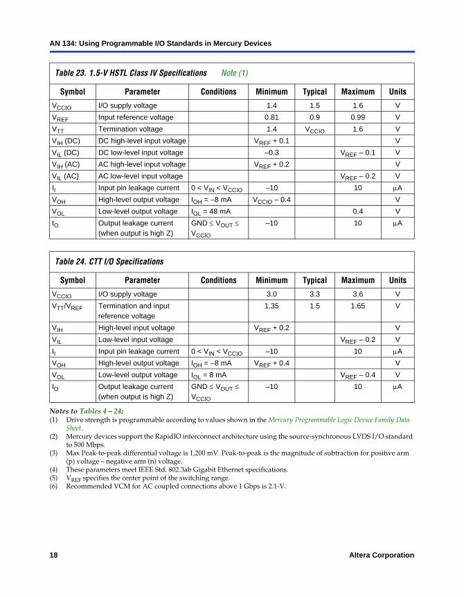
Table 23. 1.5-V HSTL Class IV Specifications Note (1)
Symbol Parameter Conditions Minimum Typical Maximum Units
VCCIO I/O supply voltage 1.4 1.5 1.6 V
VREF Input reference voltage 0.81 0.9 0.99 V
VTT Termination voltage 1.4 VCCIO 1.6 V
VIH (DC) DC high-level input voltage VREF + 0.1 V
VIL (DC) DC low-level input voltage –0.3 VREF – 0.1 V
VIH (AC) AC high-level input voltage VREF + 0.2 V
VIL (AC) AC low-level input voltage VREF – 0.2 V
II Input pin leakage current 0 < VIN < VCCIO –10 10 µA
VOH High-level output voltage IOH = –8 mA VCCIO – 0.4 V
VOL Low-level output voltage IOL = 48 mA 0.4 V
IO Output leakage current (when output is high Z)
GND ≤ VOUT ≤ VCCIO
–10 10 µA
Table 24. CTT I/O Specifications
Symbol Parameter Conditions Minimum Typical Maximum Units
VCCIO I/O supply voltage 3.0 3.3 3.6 V
VTT/VREF Termination and input reference voltage
1.35 1.5 1.65 V
VIH High-level input voltage VREF + 0.2 V
VIL Low-level input voltage VREF – 0.2 V
II Input pin leakage current 0 < VIN < VCCIO –10 10 µA
VOH High-level output voltage IOH = –8 mA VREF + 0.4 V
VOL Low-level output voltage IOL = 8 mA VREF – 0.4 V
IO Output leakage current (when output is high Z)
GND ≤ VOUT ≤ VCCIO
–10 10 µA
18 Altera Corporation
AN 134: Using Programmable I/O Standards in Mercury Devices
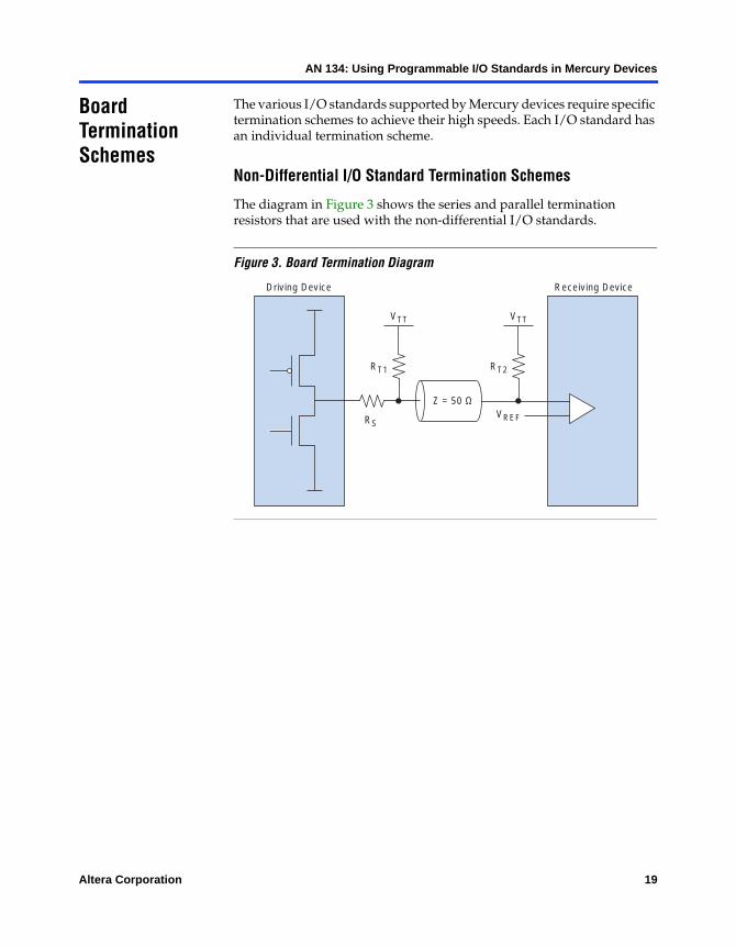
Board Termination Schemes
The various I/O standards supported by Mercury devices require specific termination schemes to achieve their high speeds. Each I/O standard has an individual termination scheme.
Non-Differential I/O Standard Termination Schemes
The diagram in Figure 3 shows the series and parallel termination resistors that are used with the non-differential I/O standards.
Figure 3. Board Termination Diagram
Driving Device Receiving Device
VTT
RS
RT1
VREF
VTT
RT2
Z = 50 Ω
Altera Corporation 19
AN 134: Using Programmable I/O Standards in Mercury Devices
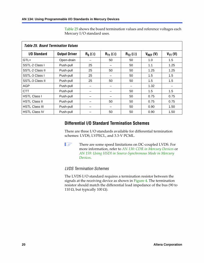
Table 25 shows the board termination values and reference voltages each Mercury I/O standard uses.
Differential I/O Standard Termination Schemes
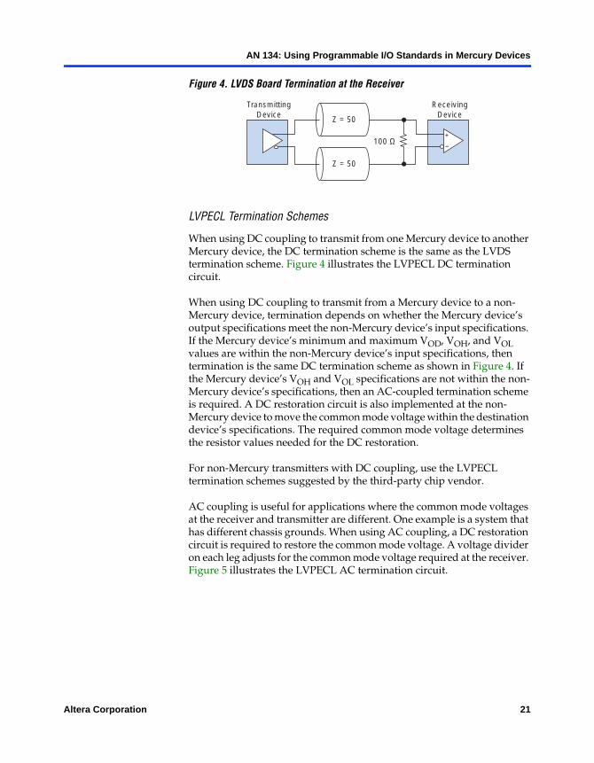
There are three I/O standards available for differential termination schemes: LVDS, LVPECL, and 3.3-V PCML.
1 There are some speed limitations on DC-coupled LVDS. For more information, refer to AN 130: CDR in Mercury Devices or AN 159: Using HSDI in Source-Synchronous Mode in Mercury Devices.
LVDS Termination Schemes
The LVDS I/O standard requires a termination resistor between the signals at the receiving device as shown in Figure 4. The termination resistor should match the differential load impedance of the bus (90 to 110 Ω, but typically 100 Ω).
Table 25. Board Termination Values
I/O Standard Output Driver RS (Ω) RT1 (Ω) RT2 (Ω) VREF (V) VTT (V)
GTL+ Open-drain – 50 50 1.0 1.5
SSTL-2 Class I Push-pull 25 – 50 1.1 1.25
SSTL-2 Class II Push-pull 25 50 50 1.25 1.25
SSTL-3 Class I Push-pull 25 – 50 1.5 1.5
SSTL-3 Class II Push-pull 25 50 50 1.5 1.5
AGP Push-pull – – – 1.32 –
CTT Push-pull – – 50 1.5 1.5
HSTL Class I Push-pull – – 50 0.75 0.75
HSTL Class II Push-pull – 50 50 0.75 0.75
HSTL Class III Push-pull – – 50 0.90 1.50
HSTL Class IV Push-pull – 50 50 0.90 1.50
20 Altera Corporation
AN 134: Using Programmable I/O Standards in Mercury Devices
Figure 4. LVDS Board Termination at the Receiver
LVPECL Termination Schemes
When using DC coupling to transmit from one Mercury device to another Mercury device, the DC termination scheme is the same as the LVDS termination scheme. Figure 4 illustrates the LVPECL DC termination circuit.
When using DC coupling to transmit from a Mercury device to a non-Mercury device, termination depends on whether the Mercury device’s output specifications meet the non-Mercury device’s input specifications. If the Mercury device’s minimum and maximum VOD, VOH, and VOL values are within the non-Mercury device’s input specifications, then termination is the same DC termination scheme as shown in Figure 4. If the Mercury device’s VOH and VOL specifications are not within the non-Mercury device’s specifications, then an AC-coupled termination scheme is required. A DC restoration circuit is also implemented at the non-Mercury device to move the common mode voltage within the destination device’s specifications. The required common mode voltage determines the resistor values needed for the DC restoration.
For non-Mercury transmitters with DC coupling, use the LVPECL termination schemes suggested by the third-party chip vendor.
AC coupling is useful for applications where the common mode voltages at the receiver and transmitter are different. One example is a system that has different chassis grounds. When using AC coupling, a DC restoration circuit is required to restore the common mode voltage. A voltage divider on each leg adjusts for the common mode voltage required at the receiver. Figure 5 illustrates the LVPECL AC termination circuit.
Z = 50
Z = 50
TransmittingDevice
ReceivingDevice
+
–100 Ω
Altera Corporation 21
AN 134: Using Programmable I/O Standards in Mercury Devices
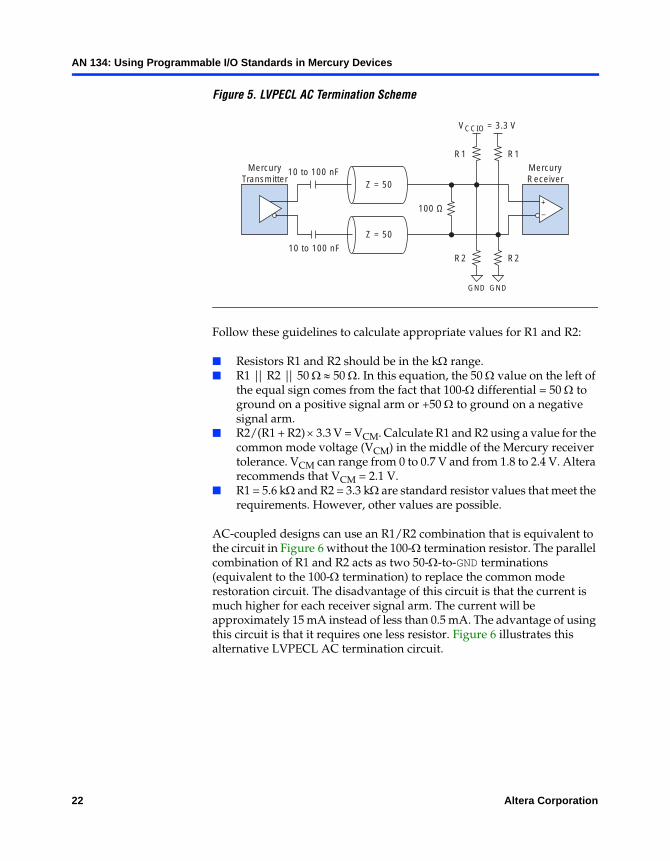
Figure 5. LVPECL AC Termination Scheme
Follow these guidelines to calculate appropriate values for R1 and R2:
Resistors R1 and R2 should be in the kΩ range. R1 || R2 || 50 Ω ≈ 50 Ω. In this equation, the 50 Ω value on the left of
the equal sign comes from the fact that 100-Ω differential = 50 Ω to ground on a positive signal arm or +50 Ω to ground on a negative signal arm.
R2/(R1 + R2) × 3.3 V = VCM. Calculate R1 and R2 using a value for the common mode voltage (VCM) in the middle of the Mercury receiver tolerance. VCM can range from 0 to 0.7 V and from 1.8 to 2.4 V. Altera recommends that VCM = 2.1 V.
R1 = 5.6 kΩ and R2 = 3.3 kΩ are standard resistor values that meet the requirements. However, other values are possible.
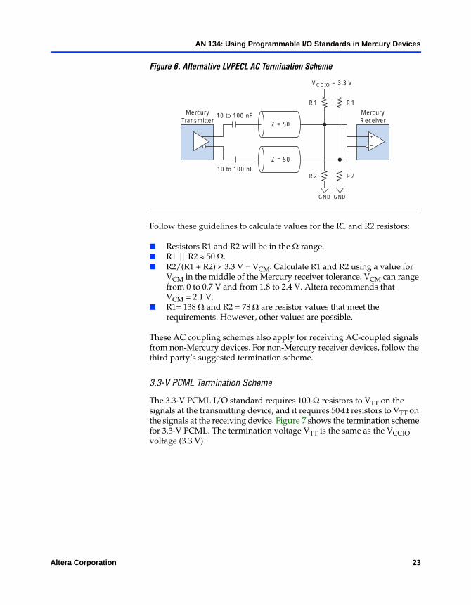
AC-coupled designs can use an R1/R2 combination that is equivalent to the circuit in Figure 6 without the 100-Ω termination resistor. The parallel combination of R1 and R2 acts as two 50-Ω-to-GND terminations (equivalent to the 100-Ω termination) to replace the common mode restoration circuit. The disadvantage of this circuit is that the current is much higher for each receiver signal arm. The current will be approximately 15 mA instead of less than 0.5 mA. The advantage of using this circuit is that it requires one less resistor. Figure 6 illustrates this alternative LVPECL AC termination circuit.
Z = 50
Z = 50
MercuryTransmitter
MercuryReceiver
+
–100 Ω
10 to 100 nF
10 to 100 nF
GNDGND
VCCIO = 3.3 V
R1 R1
R2 R2
22 Altera Corporation
AN 134: Using Programmable I/O Standards in Mercury Devices
Figure 6. Alternative LVPECL AC Termination Scheme
Follow these guidelines to calculate values for the R1 and R2 resistors:
Resistors R1 and R2 will be in the Ω range. R1 || R2 ≈ 50 Ω. R2/(R1 + R2) × 3.3 V = VCM. Calculate R1 and R2 using a value for
VCM in the middle of the Mercury receiver tolerance. VCM can range from 0 to 0.7 V and from 1.8 to 2.4 V. Altera recommends that VCM = 2.1 V.
R1= 138 Ω and R2 = 78 Ω are resistor values that meet the requirements. However, other values are possible.
These AC coupling schemes also apply for receiving AC-coupled signals from non-Mercury devices. For non-Mercury receiver devices, follow the third party’s suggested termination scheme.
3.3-V PCML Termination Scheme
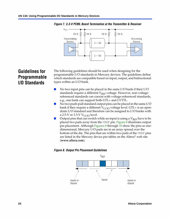
The 3.3-V PCML I/O standard requires 100-Ω resistors to VTT on the signals at the transmitting device, and it requires 50-Ω resistors to VTT on the signals at the receiving device. Figure 7 shows the termination scheme for 3.3-V PCML. The termination voltage VTT is the same as the VCCIO voltage (3.3 V).
Z = 50
Z = 50
MercuryTransmitter
MercuryReceiver
+
–
10 to 100 nF
10 to 100 nF
GNDGND
VCCIO = 3.3 V
R1 R1
R2 R2
Altera Corporation 23
AN 134: Using Programmable I/O Standards in Mercury Devices
Figure 7. 3.3-V PCML Board Termination at the Transmitter & Receiver
Guidelines for Programmable I/O Standards
The following guidelines should be used when designing for the programmable I/O standards in Mercury devices. The guidelines define which standards are compatible based on input, output, and bidirectional types within an I/O bank.
No two input pins can be placed in the same I/O bank if their I/O standards require a different VREF voltage. However, non-voltage-referenced standards can coexist with voltage-referenced standards, e.g., one bank can support both GTL+ and LVTTL.
No two push-pull standard output pins can be placed in the same I/O bank if they require a different VCCIO voltage level. GTL+ is an open-drain I/O standard and therefore can be assigned to I/O banks with a 2.5-V or 3.3-V VCCIO level.
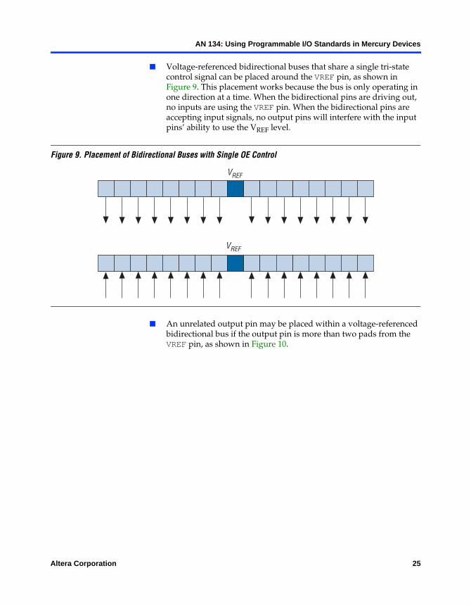
Output pins that can switch while an input is using a VREF have to be placed two pads away from the VREF pin. Figure 8 illustrates output pin placement. Although Figures 8 through 10 show the pins as one-dimensional, Mercury I/O pads are in an array spread over the bottom of the die. The pins that are within two pads of the VREF pins are listed in the Mercury device pin tables on the Altera® web site (www.altera.com).
Figure 8. Output Pin Placement Guidelines
Z = 50
Z = 50
TransmittingDevice
ReceivingDevice
+
–
50 Ω50 Ω50 Ω50 Ω
VTT
VREF
Inputs Inputs orOuputs
Inputs orOuputs
24 Altera Corporation
AN 134: Using Programmable I/O Standards in Mercury Devices
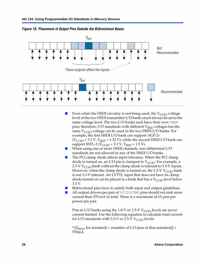
Voltage-referenced bidirectional buses that share a single tri-state control signal can be placed around the VREF pin, as shown in Figure 9. This placement works because the bus is only operating in one direction at a time. When the bidirectional pins are driving out, no inputs are using the VREF pin. When the bidirectional pins are accepting input signals, no output pins will interfere with the input pins’ ability to use the VREF level.
Figure 9. Placement of Bidirectional Buses with Single OE Control
An unrelated output pin may be placed within a voltage-referenced bidirectional bus if the output pin is more than two pads from the VREF pin, as shown in Figure 10.
VREF
VREF
Altera Corporation 25
AN 134: Using Programmable I/O Standards in Mercury Devices
Figure 10. Placement of Output Pins Outside the Bidirectional Buses
Even when the HSDI circuitry is not being used, the VCCIO voltage level of the two HSDI transmitter I/O banks must always be set to the same voltage level. The two I/O banks each have their own VREF pins; therefore, I/O standards with different VREF voltages but the same VCCIO voltage can be used in the two HSDI I/O banks. For example, the first HSDI I/O bank can support AGP 2× (VCCIO = 3.3 V, VREF = 1.32 V), while the second HSDI I/O bank can support SSTL-3 (VCCIO = 3.3 V, VREF = 1.5 V).
When using one or more HSDI channels, non-differential I/O standards are not allowed in any of the HSDI I/O banks.
The PCI clamp diode affects input tolerance. When the PCI clamp diode is turned on, an I/O pin is clamped to VCCIO. For example, a 2.5-V VCCIO bank without the clamp diode is tolerant to 3.3-V inputs. However, when the clamp diode is turned on, the 2.5-V VCCIO bank is not 3.3-V tolerant. An LVTTL input that does not have its clamp diode turned on can be placed in a bank that has a VCCIO level below 3.3 V.
Bidirectional pins have to satisfy both input and output guidelines. All output drivers per pair of VCCIO/GND pins should not sink more
current than 570 mA in total. There is a maximum of 15 pins per power pin pair.
Pins in I/O banks using the 1.8-V or 1.5-V VCCIO levels are never current-limited. Use the following equation to calculate total current for I/O standards with 3.3-V or 2.5-V VCCIO levels:
² [(IMAX for standard) × (number of I/O pins of that standard)] < 570mA
These outputs affect the inputs
NotRecommended
Recommended
VREF
VREF
26 Altera Corporation
AN 134: Using Programmable I/O Standards in Mercury Devices
Table 26 shows the IMAX values.
In practice, this rule applies only to GTL+ pins, which may sink more than 45 mA per output pin. For other standards, every pin in an I/O bank can be used without violating this requirement.
1 Refer to the Mercury pin tables on the Altera web site (www.altera.com) to view the grouping of I/O pins to power pin pairs.
Software Support
The Altera Quartus® II software provides software support for the programmable I/O standards. This section shows how to implement and view the programmable I/O standards for Mercury devices in the Quartus II software and give placement and assignment guidelines, including:
Device and Pin Options Dialog Box Pin Assignments Dialog Box Representation of I/O banks and I/O standards in the Floorplan
Editor HSDI and general PLL paired pin labeling Automatic placement
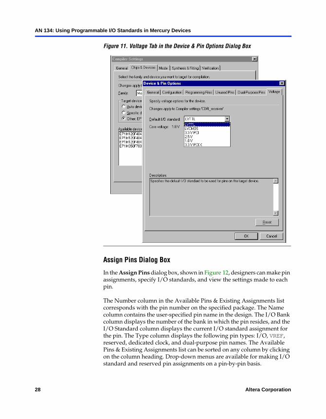
Device & Pin Options Dialog Box
The Voltage tab in the Device & Pin Options dialog box which is available from the Compiler Settings dialog box (Processing menu) contains a Default I/O standard drop-down menu, used to set the default I/O standard for a device. All I/O pins without a specific I/O standard assignment will default to the I/O standard specified in this drop-down menu. Figure 11 shows the Device & Pin Options dialog box when targeting a Mercury device.
Table 26. IMAX Values
I/O Standard IMAX (mA)
3.3-V VCCIO 2.5-V VCCIO
LVTTL 22 15
PCI, PCI-X, AGP 21 –
GTL+ 46 44
SSTL-3 30 –
SSTL-2, class I – 17
SSTL-2, class II – 25
Altera Corporation 27
AN 134: Using Programmable I/O Standards in Mercury Devices
Figure 11. Voltage Tab in the Device & Pin Options Dialog Box
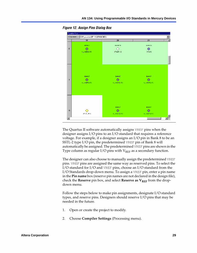
Assign Pins Dialog Box
In the Assign Pins dialog box, shown in Figure 12, designers can make pin assignments, specify I/O standards, and view the settings made to each pin.
The Number column in the Available Pins & Existing Assignments list corresponds with the pin number on the specified package. The Name column contains the user-specified pin name in the design. The I/O Bank column displays the number of the bank in which the pin resides, and the I/O Standard column displays the current I/O standard assignment for the pin. The Type column displays the following pin types: I/O, VREF, reserved, dedicated clock, and dual-purpose pin names. The Available Pins & Existing Assignments list can be sorted on any column by clicking on the column heading. Drop-down menus are available for making I/O standard and reserved pin assignments on a pin-by-pin basis.
28 Altera Corporation
AN 134: Using Programmable I/O Standards in Mercury Devices
Figure 12. Assign Pins Dialog Box
The Quartus II software automatically assigns VREF pins when the designer assigns I/O pins to an I/O standard that requires a reference voltage. For example, if a designer assigns an I/O pin in Bank 8 to be an SSTL-2 type I/O pin, the predetermined VREF pin of Bank 8 will automatically be assigned. The predetermined VREF pins are shown in the Type column as regular I/O pins with VREF as a secondary function.
The designer can also choose to manually assign the predetermined VREF pins. VREF pins are assigned the same way as reserved pins. To select the I/O standard for I/O and VREF pins, choose an I/O standard from the I/O Standards drop-down menu. To assign a VREF pin, enter a pin name in the Pin name box (reserve pin names are not declared in the design file), check the Reserve pin box, and select Reserve as VREF from the drop-down menu.
Follow the steps below to make pin assignments, designate I/O standard types, and reserve pins. Designers should reserve I/O pins that may be needed in the future.
1. Open or create the project to modify.
2. Choose Compiler Settings (Processing menu).
Altera Corporation 29
AN 134: Using Programmable I/O Standards in Mercury Devices
3. Click the Chips & Devices tab.
4. Select the target device in the Available devices list.
5. Click Assign Pins.
6. In the Assign Pins dialog box, to show the pins for which you cannot assign a node name in the Available Pins & Existing Assignments list, turn on Show no connect pins.
7. In the Available pins & existing assignments list, select the pin number for the pin to which you want to assign, change, or delete a node name assignment.
8. If there is an existing assignment to the selected pin, click Delete under Assignment to delete the node name assignment from the pin.
9. To assign a new node name to the pin, or change the existing node name assignment for the pin, under Assignment, type a node name in the Pin name box or copy the node name to the Assign Pins dialog box with the Node Finder.
10. If you added or changed the node name assignment for the pin and you want to assign an I/O standard to the pin, under Assignment, select a standard from the I/O Standard list.
11. If you added or changed the node name assignment or I/O standard and you want to reserve the pin for future use or reserve a pin that does not yet exist in the design file, under Assignment, turn on Reserve pin. Select As input tri-stated, As output driving ground, As output driving an unspecified signal, or As VREF from the Reserve pin menu.
12. To save a new assignment and add the assignment to the Available pins & existing assignments list, under Assignment, click Add.
13. To save the changed assignment and add the assignment to the Available pins & existing assignments list, under Assignment, click Change.
14. Repeat steps 7 to 13 for each additional assignment you want to make, change, or delete.
15. Click OK.
30 Altera Corporation
AN 134: Using Programmable I/O Standards in Mercury Devices
In addition to the Assign Pins dialog box, I/O standards can be assigned through the Assignment Organizer dialog box (Tools menu). The advantage to using the Assign Pins dialog box is that pin assignments and I/O standard assignments can be set in one dialog box. To make an I/O standard assignment without assigning the node to a pin, use the Assignment Organizer dialog box.
I/O Banks & Standards in the Floorplan Editor
The Floorplan Editor supports many features in Mercury devices, including multiple I/O standards, PLLs, and the HSDI circuitry. The Floorplan Editor shows membership in I/O banks by using a unique background fill color around each pin for each I/O bank. In addition, the bank number is shown. The Floorplan Editor has two package views (Package Top, Package Bottom) and two internal views (Interior LABs and Interior Cells). In the package views, the I/O bank number is labeled above the pin. In the interior views, the I/O bank is outside the package as a background around the pin name.
Only I/O and VCCIO pins have a colored background; GNDINT, GNDIO, and VCCINT pins do not. Figure 13 shows the coloring in the Floorplan Editor for the EP1M120FC484 device in package view. The figure shows portions of two I/O banks of the device.
Altera Corporation 31
AN 134: Using Programmable I/O Standards in Mercury Devices
Figure 13. Device Package View
Under the View menu in the Floorplan Editor, the Show I/O Banks option turns on the I/O bank color display in the two interior views. This command also turns on the display of both the I/O bank colors and bank numbers in the two package views.
The Floorplan Editor Color Legend, which is located under the View menu, has an entry for each I/O pin color.
HSDI & General PLL Paired Pin Labeling
Information on the dual-purpose paired HSDI pins are displayed in the same text string as the other information on a pin, similar to other pins that have secondary functions, such as INIT_DONE. For example, in Figure 12 on page 29, I/O pin A16 is now shown as I/O, HSDI_RX1p.
32 Altera Corporation
AN 134: Using Programmable I/O Standards in Mercury Devices
HSDI pin names all begin with the prefix HSDI. The next two characters for data pins indicate whether they belong to the receiver (RX) or transmitter (TX), followed by the two-digit channel <number> ranging from 01 to 18. The last character at the end of the pin name indicates polarity: p for positive and n for negative polarity.
Table 27 summarizes all of the HSDI pin names. The dedicated clock pins (HSDI_CLK1p and HSDI_CLK2p) support HSDI and have optional dual-purpose negative polarity pins associated with them. The PLL feedback pins (CLKLK_FB1p, CLKLK_FB2p) and the general PLL output pins (CLKLK_OUT1p, CLKLK_OUT2p) follow the same convention as the dedicated clock pins.
Table 27. HSDI & General PLL Pin Naming Convention
Pin Name Function
HSDI_RX<number>p Receiver positive data pin
HSDI_RX<number>n Receiver negative data pin
HSDI_TX<number>p Transmitter positive data pin
HSDI_TX<number>n Transmitter negative data pin
HSDI_CLK1p HSDI PLL 1 input clock positive pin
HSDI_CLK1n HSDI PLL 1 input clock negative pin
HSDI_CLK2p HSDI PLL 2 input clock positive pin
HSDI_CLK2n HSDI PLL 2 input clock negative pin
HSDI_TXCLKOUTp Transmitter output clock positive pin
HSDI_TXCLKOUTn Transmitter output clock negative pin
CLK<number>p Dedicated clock positive pin
CLK<number>n Dedicated clock negative pin
CLKLK_FB<number>p Dual-purpose ClockLockTM feedback positive pin (general PLL)
CLKLK_FB<number>n Dual-purpose ClockLock feedback negative pin (general PLL)
CLKLK_OUT<number>p Dual-purpose ClockLock output positive pin (general PLL)
CLKLK_OUT<number>n Dual-purpose ClockLock output negative pin (general PLL)
Altera Corporation 33
AN 134: Using Programmable I/O Standards in Mercury Devices
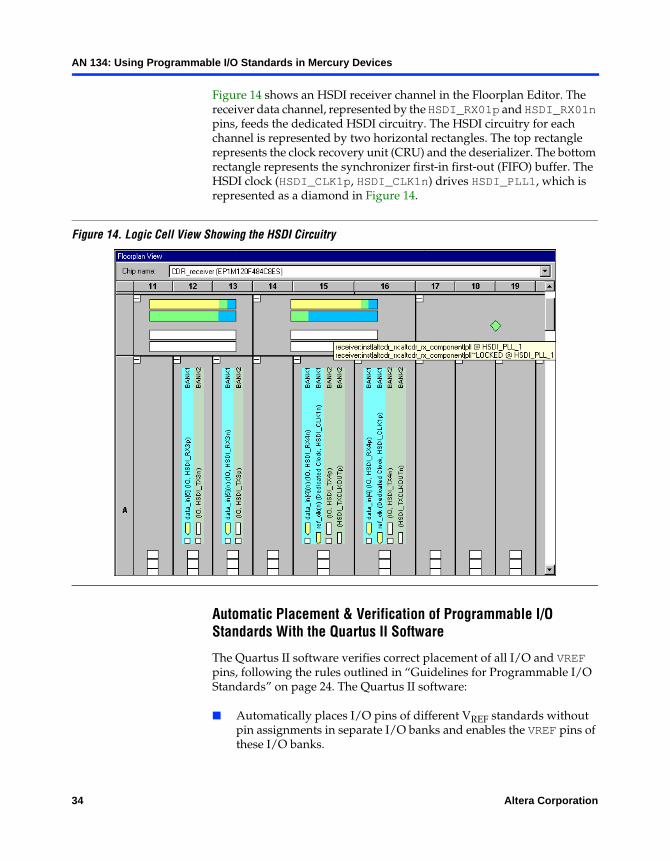
Figure 14 shows an HSDI receiver channel in the Floorplan Editor. The receiver data channel, represented by the HSDI_RX01p and HSDI_RX01n pins, feeds the dedicated HSDI circuitry. The HSDI circuitry for each channel is represented by two horizontal rectangles. The top rectangle represents the clock recovery unit (CRU) and the deserializer. The bottom rectangle represents the synchronizer first-in first-out (FIFO) buffer. The HSDI clock (HSDI_CLK1p, HSDI_CLK1n) drives HSDI_PLL1, which is represented as a diamond in Figure 14.
Figure 14. Logic Cell View Showing the HSDI Circuitry
Automatic Placement & Verification of Programmable I/O Standards With the Quartus II Software
The Quartus II software verifies correct placement of all I/O and VREF pins, following the rules outlined in “Guidelines for Programmable I/O Standards” on page 24. The Quartus II software:
Automatically places I/O pins of different VREF standards without pin assignments in separate I/O banks and enables the VREF pins of these I/O banks.
34 Altera Corporation
AN 134: Using Programmable I/O Standards in Mercury Devices
Verifies that no two voltage-referenced I/O pins requiring different VREF levels are placed in one bank.
Does not allow placement of an output pin within two pins of a VREF pin.
Reports an error message if the current limit is exceeded for a Mercury power bank, as determined by the equation documented in “Guidelines for Programmable I/O Standards” on page 24.
Reserves the unused HSDI channels and regular user I/O pins in the HSDI banks when any of the HSDI channels are being used.
Conclusion The Mercury devices’ programmable I/O features and standards simplify board design by minimizing the number of devices used to interface with memory, microprocessors, and backplanes. Mercury devices support a wide spectrum of programmable I/O standards, including LVDS, LVPECL, 3.3-V PCML, and LVTTL, allowing customization for a wide variety of applications. Input, output, and bidirectional pins of different I/O standards can be intermixed within I/O banks for additionally flexibility. Mercury devices also offer increased I/O performance with features like CDR (1.25-Gbps data transfer), double data rate I/O (DDRIO), programmable delays, and fast Mercury I/O pins.
References Interface Standard for Nominal 3 V/3.3 V Supply Digital Integrated Circuits, JESD8-A, Electronic Industries Association, June 1994.
Stub-Series Terminated Logic for 3.3 Volts (SSTL-3), EIA/JESD8-8, Electronic Industries Association, August 1996.
Stub-Series Terminated Logic for 2.5 Volts (SSTL-2), EIA/JESD8-9, Electronic Industries Association, September 1998.
Electrical Characteristics of Low Voltage Differential Signaling (LVDS) Interface Circuits, ANSI/TIA/EIA-644, American National Standards Institute/Telecommunication Industry Association/Electronic Industries Association.
2.5 V ±0.2 V (Normal Range) and 1.7 V to 2.7 V (Wide Range) Power Supply Voltage and Interface Standard for Nonterminated Digital Integrated Circuit, EIA/JESD8-5, Electronic Industries Association, October 1995.
1.8 V ±0.15 V (Normal Range) and 1.2 V to 1.95 V (Wide Range) Power Supply Voltage and Interface Standard for Nonterminated Digital Integrated Circuit, EIA/JESD8-7, Electronic Industries Association, February 1997.
PCI Local Bus Specification, Revision 2.2, PCI Special Interest Group, December 1998.
Altera Corporation 35
AN 134: Using Programmable I/O Standards in Mercury Devices
101 Innovation DriveSan Jose, CA 95134(408) 544-7000http://www.altera.comApplications Hotline:(800) 800-EPLDLiterature Services:[email protected]
Copyright © 2002 Altera Corporation. All rights reserved. Altera, The Programmable Solutions Company, thestylized Altera logo, specific device designations, and all other words and logos that are identified astrademarks and/or service marks are, unless noted otherwise, the trademarks and service marks of AlteraCorporation in the U.S. and other countries. All other product or service names are the property of theirrespective holders. Altera products are protected under numerous U.S. and foreign patents and pendingapplications, maskwork rights, and copyrights. Altera warrants performance of itssemiconductor products to current specifications in accordance with Altera's standardwarranty, but reserves the right to make changes to any products and services at any timewithout notice. Altera assumes no responsibility or liability arising out of the applicationor use of any information, product, or service described herein except as expressly agreedto in writing by Altera Corporation. Altera customers are advised to obtain the latestversion of device specifications before relying on any published information and beforeplacing orders for products or services.
Revision History
The information contained in AN 256: Implementing Double Data Rate I/O Signaling in Cyclone Devices version 1.1 supersedes information published in previous versions.
Version 2.1
The following changes were made to AN 134: Using Programmable I/O Standards in Mercury Devices version 2.1:
Change the VCM value in Table 8 from 1.2 V to 2.1 V. Updated text to Note (2) under Table 24. Updated GTL+ values in Table 25. Updated Figure 7.
36 Altera Corporation
Printed on Recycled Paper.