Embed Size (px)
Citation preview

310 IEEE TRANSACTIONS ON MICROWAVE THEORY AND TECHNIQUES, VOL. 58, NO. 2, FEBRUARY 2010
A CMOS Class-E Power Amplifier With VoltageStress Relief and Enhanced Efficiency
Yonghoon Song, Student Member, IEEE, Sungho Lee, Student Member, IEEE, Eunil Cho,Jaejun Lee, Student Member, IEEE, and Sangwook Nam, Member, IEEE
Abstract—This paper proposes a class-E power amplifier (PA)with double-resonance circuit to reduce voltage stress on CMOStransistors. The voltage waveform applied to the CMOS transistoris shaped by harmonic control and the transistors are relieved frombreakdowns. A negative capacitance is also implemented for effi-ciency enhancement, compensating for surplus capacitance fromparasitic components on the drain node. Thus, nominal class-E op-eration is restored and high efficiency is achieved. We present a cas-code differential class-E RF PA that is fabricated using a 0.13- mCMOS technology that delivers 31.5-dBm output power with 54%drain efficiency and 51% power-added efficiency at 1.8 GHz.
Index Terms—Class-E, CMOS power amplifiers (PAs), switchingamplifiers, zero voltage switching (ZVS).
I. INTRODUCTION
M OBILE equipment demands highly efficient RF trans-mitters to conserve battery life. The power amplifier
(PA) is the most critical component used to determine overall RFtransmitter efficiency because it consumes the largest portion ofdc power in the transmitter. Thus, highly efficient PAs are nec-essary to improve overall efficiency. A class-E PA is adaptablefor a high-efficiency transmitter due to its high efficiency andsimplicity. A class-E amplifier with a shunt capacitor was intro-duced by Sokal and Sokal in 1975 and was examined by Raab inan analysis of idealized operation [1], [2]. As a kind of switchingamplifier, it can achieve the ideal 100% drain (or collector) effi-ciency by shaping the voltage waveform and current waveformso that they do not overlap, making it a strong candidate for ahighly efficient RF PA [3]–[10]. Many designs have been pre-sented on new devices, such as GaAs HBTs, GaN HEMTs, andInP double HBTs (DHBTs), used to operate on microwave andhigher frequencies with better RF performances [11]–[13]. Re-cently, many researchers have been conducted about watt-leveloutput power PAs using CMOS technology on microwave dueits low cost [14]–[22].
In spite of its cost effectiveness, the CMOS PA has a seriousweakness: a low breakdown voltage. As the process scale be-comes smaller, the breakdown voltage is also reduced. As a re-
Manuscript received July 15, 2009; revised October 25, 2009. First publishedJanuary 12, 2010; current version published February 12, 2010. This work wassupported by the Korea Science and Engineering Foundation (KOSEF) underthe National Research Laboratory Program funded by the Ministry of Education,Science and Technology [ROA-2007-000-20118-0(2007)].
The authors are with the Institute of New Media Communication, Schoolof Electrical Engineering and Computer Science, Seoul National University,Seoul 151-742, Korea (e-mail: [email protected]; [email protected];[email protected]).
Color versions of one or more of the figures in this paper are available onlineat http://ieeexplore.ieee.org.
Digital Object Identifier 10.1109/TMTT.2009.2037877
Fig. 1. Basic class-E amplifier schematic with CMOS switch.
sult, supply voltage is limited to avoid breakdowns. In deliv-ering large output power under a low-supply voltage, low loadimpedance is inevitable, which causes efficiency degradationand a narrowband load matching network [15], [18].
This study presents a double-resonance circuit for harmoniccontrol, which gives relief to CMOS transistors from breakingdowns. This circuit shapes a voltage waveform applied to thetransistor gate and reduces voltage stress across the CMOStransistors. When voltage stress is reduced, the voltage marginfrom the breakdown increases, enabling the application of ahigher supply voltage. With higher supply voltage, higher loadimpedance can be implemented to deliver the same outputpower with greater efficiency.
Additionally, CMOS PAs require wide gatewidths to reduceon-resistance for high efficiency and to drive sufficient currentsfor watt-level output power. The maximum operation frequencyof class-E is also proportional to peak drain current
. For these reasons, the applicable gatewidths aresome millimeters wide [14]–[17], [21]. However, widening thegatewidth introduces undesired parasitic components, such asparasitic capacitance. Parasitic capacitance increases the valueof shunt drain capacitance , depicted in Fig. 1, whichdetermines the nominal operation condition and maximumoperation frequency of a class-E amplifier since is deter-mined by an ratio [23]. When deviates from itsoptimum value determined by the condition of nominal class-Eoperation, the efficiency degradation occurs. To maintain highefficiency, the surplus capacitance from parasitic capacitanceshould be tuned out. We set a negative capacitance using asimple capacitor to tune out surplus capacitance without addingexternal circuits.
In this paper, differential architecture is used to deliver higheroutput power than a single-ended PA. Differential architecturecan provides 3-dB more output power with the same supplyvoltage and load impedance than single-ended architecture.
0018-9480/$26.00 © 2010 IEEE
Authorized licensed use limited to: Seoul National University. Downloaded on February 13, 2010 at 03:28 from IEEE Xplore. Restrictions apply.

SONG et al.: CMOS CLASS-E PA WITH VOLTAGE STRESS RELIEF AND ENHANCED EFFICIENCY 311
Differential architecture also disturbs other circuits less than asingle-ended architecture in the same chip during the operation.Furthermore, it restrains the second harmonic at the output.An off-chip passive balun is used to transform the outputstructure from differential to single-ended.
This paper is organized as follows. Section II introducesthe fundamental theory of a class-E PA. In Section III, adouble-resonance circuit for voltage stress relief is addressed.In Section IV, we present a cascode class-E PA with negativecapacitance to compensate for the surplus . After that, weexplain our CMOS PA design in Section V, and our measure-ment results are shown in Section VI. Conclusions are given inSection VII.
II. FUNDAMENTAL THEORY OF CLASS E
The class-E amplifier is composed of a switch (usually a tran-sistor) and a shunt capacitor. Its basic schematic is shown inFig. 1 and is determined as
(1)
In addition, based on previous study, the voltage across theswitch and the current through the switch arestated as follows [24]:
(2)
(3)
The operation of class E is the charging/discharging offollowing an operating signal. For a nominal class-E oper-ation, should satisfy two conditions, which are: 1)zero voltage switching (ZVS) and 2) zero voltage derivativeswitching (ZVDS). ZVS prevents the dissipation of the energystored by the when it turns on, and ZVDS makes the circuitrobust in the face of variations in the components, frequency,and switching instants [25], [26]. When a class-E amplifieroperates in a nominal condition with a 50% duty cycle (thetransistor is on for and off for ), thevalue of is determined as 32.482 . Consequently, (2) and(3) can be written in normalized form as
(4)
(5)
where .A class-E amplifier operation with waveforms of (4) and (5)
achieves 100% drain (or collector) efficiency because, in theory,they do not create dc losses by overlapping and inthe operation. The relationship between the operation frequency
and the load impedance is calculated asin a nominal class-E operation [27].
However, in the real world, variation exists in the desiredvalue based on parasitic capacitance or process variation in
the CMOS process. Thus, the value cannot maintain0.1836 with fixed at a given frequency. When thevalues deviate from 0.1836, there is a loss in the class-E ampli-fier operation, degrading the drain (or collector) efficiency.
Fig. 2. Schematic of: (a) double-resonance circuit implementation and (b) itsac equivalent circuit.
Another characteristic of a class-E amplifier is a high-peakvoltage swing. Maximum voltage on the drain (or collector) ofthe transistor in the operation conditions given above is depictedin the following equation under a supply voltage [28]:
(6)
and the value of threatens the transistor’s reliability, es-pecially in CMOS technology, due to its low breakdown voltage.To ensure circuit reliability, several research studies have beenconducted to analyze voltage stress on CMOS transistors [15],[21]. In order to reduce voltage stress on transistors, we presenta double-resonance scheme in Section III.
III. DOUBLE-RESONANCE CIRCUIT
The double-resonance circuit shapes the voltage waveformat the transistor gate of the PA at node A in Fig. 2 using har-monic control. The voltage waveform at node B in Fig. 2 isusually induced by the switching-mode driver stage because theswitching-mode driver amplifier’s output is adaptable to drivethe class-E PA [16], [20]–[22]. Thus, the switching-mode driveramplifier operates in the nonlinear region, containing many har-monics in the output waveform. When the output signal from thedriver stage is applied to the main stage, there is only a dc-biasdifference between the driver stage output node and the mainstage input node, which are indicated as “B” and “A,” respec-tively, in Fig. 2. Thus, the waveform on node A in Fig. 2 can bewritten in general form as
(7)
where represents the coefficient of th harmonics.
Authorized licensed use limited to: Seoul National University. Downloaded on February 13, 2010 at 03:28 from IEEE Xplore. Restrictions apply.

312 IEEE TRANSACTIONS ON MICROWAVE THEORY AND TECHNIQUES, VOL. 58, NO. 2, FEBRUARY 2010
Fig. 3. Waveforms of input voltage �� � and output voltage �� � of CMOSclass-E amplifier (Fig. 1), and voltage stress reduction ��� � by double-reso-nance circuit with maintaining duty cycle (transistor threshold voltage � ��� Vand � � ��� V).
The resonance frequencies of the double-resonance circuitare fundamental frequency and second harmonic. The controlof these harmonics shapes the voltage waveform , as de-scribed in Fig. 3, by reducing even harmonics. The double-res-onance circuit trespasses fundamental frequency and third har-monic from driver stage to the main stage and removes thesecond harmonic.
Since the voltage of the drain (or collector) hits its peak value(theoretically in a 50% duty cycle) when the switchis in the off state, the highest voltage stress is applied across thegate–oxide during this period (see Fig. 3). Applying the double-resonance circuit increases the dc offset of and does notallow to stay too far below the transistor’s threshold voltageduring the off state, without deteriorating the duty cycle. There-fore, a higher in the off state decreases maximum voltagestress across the transistor.
This voltage shaping by the double-resonance circuit usingharmonic control differs from dc-bias increasing. DC-biasincreasing changes the duty cycle of the amplifier and differentduty cycles have different drain (or collector) peak voltages[10]. As the duty cycle increases, the peak voltage also in-creases, and it worsens the voltage stress on the transistor.However, voltage shaping via harmonic control exhibits thesame duty cycle in 0.5-V threshold voltage transistors in Fig. 3and allows the PA to maintain its performance.
Above all, our double-resonance circuit using harmoniccontrol relieves transistors from breakdowns through voltagestress reduction. In a CMOS class-E amplifier with 1.0-Vsupply voltage, voltage stress is reduced about 0.3 V from 4.3to 4.0 V in simulation. Furthermore, eliminating the secondharmonic and trespassing odd harmonics (fundamental fre-quency and third harmonic) moves to have faster risingand falling times, which aids in switching the amplifier’soperation.
To implement the double-resonance circuit, we used two res-onators. One is the parallel resonator consisting of gate
Fig. 4. Normalized voltage � (on transistor drain) and current � (flowing tran-sistor) waveforms of class E for different values of �� � with 50% dutycycle.
inductor and main stage input capacitance , as de-scribed in Fig. 2. It is designed to resonate at the fundamentalfrequency to drive the main amplifier efficiently, overcominglarge input capacitance. The other resonator is a series res-onator attached to the output node of driver stage, re-jecting the second harmonic and trespassing the fundamentalfrequency and third harmonic at node B in Fig. 2. With theproposed double-resonance circuit, transistors are relieved frombreakdowns and obtain margins to increase supply voltagein the main stage of operation.
Higher supply voltage brings enhanced PA performance. Ob-viously, a PA with a higher supply voltage delivers a greateroutput power with the same load impedance. In addition, inwatt-level output power CMOS PAs, load impedance is usuallya few ohms, and thus, a higher ratio of impedance transformeris required to obtain higher output power. However, when ahigher supply voltage can be applied using this double-reso-nance scheme, a higher load impedance can be implemented forthe same output power with efficiency enhancement.
IV. NEGATIVE CAPACITANCE
A. Shunt Capacitance Analysis
As we stated in Section II, efficiency declines when thevalue deviates from its optimum value and we derived
the relationship between and as
(8)
which has an inverse proportion between and . Whenincreases from 0.1836, decreases and the transistor
drain voltage is a positive value at . On the other side,when decreases from 0.1836, increases, resulting ina negative drain voltage at . The waveforms ofand in a single period are shown in Fig. 4 for different
values when 50% duty cycle is applied. The transistoris on for and off for . When
Authorized licensed use limited to: Seoul National University. Downloaded on February 13, 2010 at 03:28 from IEEE Xplore. Restrictions apply.

SONG et al.: CMOS CLASS-E PA WITH VOLTAGE STRESS RELIEF AND ENHANCED EFFICIENCY 313
the ZVS condition is not satisfied is not 0.1836), thevoltage and current waveforms will overlap at the beginning ofthe next period because transient time is required to have zerovoltage across the transistor drain and source. This transitiontime results in a loss during the finite transient time [29]. There-fore, with the given frequency and fixed value shouldbe maintained with optimum value to achieve high efficiency inthe class-E amplifier.
B. Negative Capacitance
In the field of a CMOS PA, a large gatewidth is inevitable indelivering watt-level output power. The gatewidths are somemillimeters wide and these wide transistors contain picofaradcapacitance on the drain node. This adds parasitic capacitanceon , increasing from its desired optimum value andresulting in drain efficiency (DE) degradation. In addition, inthe class-E CMOS amplifier, cascode topology is preferred forits reliability due to the characteristic of high-peak voltage.The additional common-gate (CG) amplifier usually has a largegatewidth to reduce on-resistence and it also contributes to theincrease of . Thus, as increases, compensation for sur-plus capacitance is more significant for efficiency restoration.
To maintain the optimum value, surplus capacitanceshould be tuned out. One of the techniques used to tune outsurplus capacitance is to place an inductor on the same nodewith a dc block [21]. However, the inductor requires a largearea to be implemented into an integrated circuit. Moreover,it contains parasitic components, such as parasitic capacitanceand resistance in itself, and has a low quality factor ( factor).Therefore, we use negative capacitance to tune out surplusin cascode topology.
Basically, negative capacitance works in the same manneras polarity-inversed Miller capacitance. Miller capacitance isstated as
(9)
where indicates the voltage gain of the ’s nodes. Conven-tional is applied with negative , increasing capacitance to
times . On the contrary, we applied positive toobtain negative capacitance. The realization of negative capac-itance is shown in Fig. 5(a), as noted by . Since is con-nected between the input and output CG amplifier, which haspositive gain , it generates negative capacitance on nodeA, as described in Fig. 5(b). This negative capacitance compen-sates for surplus capacitance on node A in Fig. 5, adjustingto optimum value and restoring nominal class-E PA operation.
Negative capacitance using a capacitor benefits the integratedCMOS PA. A capacitor demands a much smaller area than an in-ductor and has a higher factor with less parasitic componentsthan an inductor. Moreover, it can be tuned by arraying parallelcapacitors with switches and requires a very small value thanksto CG amplifier gain .
Parasitic capacitance on node B is not as much of a concernas that of node A because the value of parasitic capacitance on
Fig. 5. Schematic of: (a) negative capacitance realization and (b) its equivalentcircuit.
node B is smaller than that on node A in Fig. 5. In addition,the CG amplifier is always turned on to reduce on-resistence somost of the capacitor charging/discharging occurs at node A inFig. 5 based on the switching operation.
V. CIRCUIT DESIGN
A. Main Stage
A class-E amplifier has high peak voltage across the transistorso the voltage stress on CMOS transistors should be consideredcarefully. For this reason, we adopt cascode topology to ensurefreedom from breakdowns because the cascode structure divideslarge output voltage swing into two series transistors [15].
For the given standard 0.13- m CMOS process, the foundryprovided two different types of transistors, which are: 1) a thingate–oxide transistor, which has a 0.13- m gate length for 1.2-Vsupply voltage and 2) a thick gate–oxide transistor, which hasa 0.34- m gate length for 3.3-V supply voltage. We used a thingate–oxide transistor as the common source (CS) amplifier anda thick gate–oxide transistor as the CG amplifier to ensure thebest performance.
This combination works better than two thick gate–oxidetransistors because the thin gate–oxide transistor demonstratesa better RF performance and has smaller on-resistence than thethick gate–oxide transistor. Better RF performance alleviatesthe complexity of the driver amplifier and leads to higheroperation efficiency. Furthermore, it contains fewer parasiticcomponents such as drain capacitance, which affects increaseof the value. In this study, we used 4000- m gatewidthtransistors for the CS amplifier.
For the CG amplifier, we used a thick gate–oxide transistorfor its sustainability. In class-E cascode topology, large voltageswing is applied on the CG amplifier [21]. Thick gate–oxidetransistors prevent breakdowns and they are biased to be on-stateall the time, lowering on-resistence to maintain high efficiency.
Authorized licensed use limited to: Seoul National University. Downloaded on February 13, 2010 at 03:28 from IEEE Xplore. Restrictions apply.

314 IEEE TRANSACTIONS ON MICROWAVE THEORY AND TECHNIQUES, VOL. 58, NO. 2, FEBRUARY 2010
Fig. 6. Schematic of proposed differential PA with cascode topology, includingdriver amplifiers and input balun, realized in a 0.13-�m CMOS technology.
For the CG amplifier, total gatewidths of 7000- m transistorswere implemented. The entire schematic is described in Fig. 6.
B. Driver Stage
For the driver stage, a class-E amplifier is implemented. Sincea class-E amplifier has a large voltage swing on its output, it candrive the main amplifier sufficiently with low supply voltage.Low supply voltage on the driver amplifier consumes low dcpower so it reduces efficiency degradation from DE to power-added efficiency (PAE). Double-resonance circuit is also con-sidered for designing load impedance of the driver stage. In thisstudy, the difference in efficiency between DE and PAE is only3–4 %-points. We also chose cascode topology to prevent break-downs of the thin gate–oxide transistors, which have 200- mgatewidths.
In addition, a transformer was implemented on a chip as aninput balun. This transformed the single-ended structure to adifferential structure in order to drive differential amplifiers.
C. Double-Resonance Circuit
Shaping the voltage waveform at the input of the main ampli-fier was accomplished by using a double-resonance circuit. Asdescribed in Section III, an inductor on the main amplifier gatewas used as part of the resonance circuit and it resonated withthe main amplifier input capacitance at the operation frequency.
Fig. 7. Chip photograph of proposed CMOS class-E PA.
The other resonator is attached on the output of driver amplifierusing the series resonator. This series resonator deprives thesecond harmonic from the signal flowing to the main amplifierinput and allows the third harmonic to trespass into the mainamplifier.
The proposed double-resonance circuit reduces voltagestress on the CS amplifier implemented with a thin gate–oxidetransistor on the main stage cascode structure, and shapes thevoltage waveform without deteriorating the PA performanceand duty cycle. We simulated its effectiveness using the Ad-vanced Design System (ADS) and 0.2-V voltage stress wasrelieved from the CMOS transistor.
D. Negative Capacitance
The negative capacitance is connected to the input andoutput of the CG amplifier in the main stage. It compensates forsurplus capacitance on , restoring it to its optimum value.This scheme provides negative capacitance simply with a ca-pacitor, without an additional circuit, to generate negative ca-pacitance.
There is tradeoff between the value of and stability be-cause provides a feedback path on the CG amplifier. How-ever, thanks to the CG amplifier gain , the required capaci-tance value of is small and a 1.0-pF capacitor was insertedin our design. On simulation assisted by ADS, stability degra-dation was not observed. In addition, this negative capacitancecompensated about 10.0 pF of and PAE was enhanced byabout 6 %-points in simulation.
VI. MEASUREMENT AND RESULTS
The proposed PA, including the driver stage and input balun,is fabricated using the 0.13- m standard CMOS process. Thechip photograph is shown in Fig. 7. The die area, including thebonding pads, is 1.0 mm . We used multiple bonding pads tominimize the effects from bonding inductance variation. Twelvepads were implemented to reduce ground resistance and providePA heat sink. Off-chip passive components were implementedon an FR4 printed circuit board (PCB).
Authorized licensed use limited to: Seoul National University. Downloaded on February 13, 2010 at 03:28 from IEEE Xplore. Restrictions apply.
SONG et al.: CMOS CLASS-E PA WITH VOLTAGE STRESS RELIEF AND ENHANCED EFFICIENCY 315
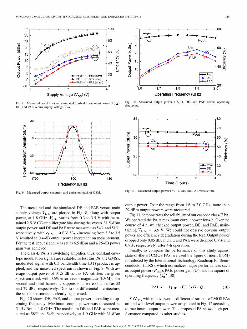
Fig. 8. Measured (solid line) and simulated (dashed line) output power (� ),DE, and PAE versus supply voltage � .
Fig. 9. Measured output spectrum and emission mask of GSM.
The measured and the simulated DE and PAE versus mainsupply voltage are plotted in Fig. 8, along with outputpower, at 1.8 GHz. varies from 0.3 to 3.5 V with main-tained 2.5-V CG amplifier gate bias during the sweep. 31.5-dBmoutput power, and DE and PAE were measured as 54% and 51%,respectively, with V. increasing from 3.3 to 3.5V resulted in 0.4-dB output power increment on measurement.For the test, input signal was set as 6.5 dBm and a 25-dB powergain was achieved.
The class-E PA is a switching amplifier, thus, constant enve-lope modulation signals are suitable. To test this PA, the GMSKmodulated signal with 0.3 bandwidth time (BT) product is ap-plied, and the measured spectrum is shown in Fig. 9. With av-erage output power of 31.5 dBm, this PA satisfies the givenspectrum mask with 0.6% error vector magnitude (EVM). Thesecond and third harmonic suppressions were obtained as 52and 29 dBc, respectively. Due to the differential architecture,the second harmonic is clearly suppressed.
Fig. 10 shows DE, PAE, and output power according to op-erating frequency. Maximum output power was measured as31.5 dBm at 1.8 GHz. The maximum DE and PAE were mea-sured as 58% and 54%, respectively, at 1.9 GHz with 31-dBm
Fig. 10. Measured output power (� ), DE, and PAE versus operatingfrequency.
Fig. 11. Measured output power (� ), DE, and PAE versus time.
output power. Over the range from 1.6 to 2.0 GHz, more than29-dBm output powers were measured.
Fig. 11 demonstrates the reliability of our cascode class-E PA.We operated the PA at maximum output power for 4 h. Over thecourse of 4 h, we checked output power, DE, and PAE, main-taining V. We could not observe obvious outputpower and efficiency degradation during the test. Output powerdropped only 0.05 dB, and DE and PAE were dropped 0.7% and0.8%, respectively, after 4-h operation.
Finally, to compare the performance of this study againststate-of-the-art CMOS PAs, we used the figure of merit (FoM)introduced by the International Technology Roadmap for Semi-conductor (ITRS), which normalizes major performances suchas output power ( ), PAE, power gain ( ), and the square ofoperating frequency [30]
(10)
with relative works, differential structure CMOS PAsaround watt-level output power, are plotted in Fig. 12 accordingto maximum output power. This proposed PA shows high per-formance compared to other studies.
Authorized licensed use limited to: Seoul National University. Downloaded on February 13, 2010 at 03:28 from IEEE Xplore. Restrictions apply.

316 IEEE TRANSACTIONS ON MICROWAVE THEORY AND TECHNIQUES, VOL. 58, NO. 2, FEBRUARY 2010
Fig. 12. Comparison of watt-level CMOS PAs (differential structure) throughITRS ��� . * indicates integrated output balun.
VII. CONCLUSION
In this paper, we presented a differential class-E PA, in-cluding a double-resonance circuit using harmonic control, andit reduced voltage stress on the transistors. We also used a neg-ative capacitance to compensate for surplus capacitance on thedrain of a class-E amplifier in order to achieve high efficiencywith cascode topology. This amplifier delivers 31.5-dBmoutput power with 54% DE and 51% PAE at 1.8 GHz using the0.13- m standard CMOS process. There was almost no perfor-mance degradation during 4-h maximum power operation.
REFERENCES
[1] N. O. Sokal and A. D. Sokal, “Class E—A new class of high-efficiencytuned single-ended switching power amplifiers,” IEEE J. Solid-StateCircuits, vol. SC-10, no. 6, pp. 168–176, Jun. 1975.
[2] F. H. Raab, “Idealized operation of the class E tuned power amplifier,”IEEE Trans. Circuits Syst., vol. CAS-24, no. 12, pp. 725–735, Dec.1977.
[3] N. Kumar, C. Prakash, A. Grebennikov, and A. Mediano, “High-effi-ciency broadband parallel-circuit class E RF power amplifier with re-actance-compensation technique,” IEEE Trans. Microw. Theory Tech.,vol. 56, no. 3, pp. 604–612, Mar. 2008.
[4] M. Kazimierczuk and K. Puczko, “Exact analysis of class E tunedpower amplifier at any� and switch duty cycle,” IEEE Trans. CircuitsSyst., vol. CAS-34, no. 2, pp. 149–158, Feb. 1987.
[5] A. V. Grebennikov, “Class E high-efficiency power amplifiers: Histor-ical aspect and future prospect,” Appl. Microw. Wireless, vol. 14, no.72, pp. 64–71, Jul.–Aug. 2002.
[6] C.-H. Li and Y.-O. Yam, “Maximum frequency and optimum perfor-mance of class E power amplifiers,” Proc. Inst. Elect. Eng.—CircuitsDevices Syst., vol. 141, pp. 174–184, Jun. 1994.
[7] A. J. Wilkinson and K. A. Everard, “Transmission line load networktopology for class E power amplifiers,” IEEE Trans. Microw. TheoryTech., vol. 49, no. 6, pp. 1202–1210, Jun. 2001.
[8] T. Tuetsugu and M. L. Kazimierczuk, “Analysis and design of classE amplifier with shunt capacitance composed of nonlinear and linearcapacitances,” IEEE Trans. Circuits Syst. I, Reg. Papers, vol. 51, no. 7,pp. 1261–1268, Jul. 2004.
[9] P. Alinikula, K. Choi, and I. Long, “Design of class E power ampli-fier with nonlinear parasitic output capacitance,” IEEE Trans. CircuitsSyst. II, Analog Digit. Signal Process., vol. 46, no. 2, pp. 114–119, Feb.1999.
[10] A. Mediano, P. Molina-Gaudó, and C. Bernal, “Design of class E am-plifier with nonlinear and linear shunt capacitances for any duty cycle,”IEEE Trans. Microw. Theory Tech., vol. 55, no. 3, pp. 484–492, Mar.2007.
[11] J. Jeon, J. Kim, and Y. Kwon, “Temperature compensating bias circuitfor GaAs HBT RF power amplifiers with a stage bypass architecture,”Electron. Lett., vol. 44, no. 19, pp. 1141–1143, Sep. 2008.
[12] S. Gao, H. Xu, S. Heikman, U. K. Mishra, and R. A. York, “Two-stagequasi-class-E power amplifier in GaN HEMT technology,” IEEE Mi-crow. Wireless Compon. Lett., vol. 16, no. 1, pp. 28–30, Jan. 2006.
[13] P. Watson et al., “An indium phosphide�-band class-E power MMICwith 40% bandwidth,” in IEEE Compound Semiconduct. Integr. Cr-cuits. Symp., Palm Springs, CA, Nov. 2005, pp. 220–223.
[14] K.-C. Tsai and P. R. Gray, “A 1.9-GHz, 1-W CMOS class-E poweramplifier for wireless communications,” IEEE J. Solid-State Circuit,vol. 34, no. 7, pp. 962–970, Jul. 1999.
[15] C. Yoo and Q. Huang, “A common-gate switched 0.9-W class-E poweramplifier with 41% PAE in 0.25-�m CMOS,” IEEE J. Solid-State Cir-cuits, vol. 36, no. 5, pp. 823–830, May 2001.
[16] J. Jang, C. Park, H. Kim, and S. Hong, “A CMOS RF power ampli-fier using an off-chip transmision line transformer with 62% PAE,”IEEE Microw. Wireless Compon. Lett., vol. 17, no. 5, pp. 385–387,May 2007.
[17] R. Brama, L. Larcher, A. Mazzanti, and F. Svelto, “A 30.5 dBm 48%PAE CMOS class-E PA with integrated balun for RF applications,”IEEE J. Solid-State Circuits., vol. 43, no. 8, pp. 1755–1762, Aug. 2008.
[18] K. L. R. Mertens and M. S. J. Steyaert, “A 700-MHz, 1-W fully dif-ferential CMOS class-E power amplifier,” IEEE J. Solid-State Circuits,vol. 37, no. 1, pp. 137–141, Jan. 2006.
[19] R. Negra and W. Bächtold, “Lumped-element load-network design forclass-E power amplifiers,” IEEE Trans. Microw. Theory Tech., vol. 54,no. 6, pp. 2684–2690, Jun. 2006.
[20] M. Apostolidou et al., “A 65 nm CMOS 30 dBm class-E RF power am-plifier with 60% power added efficiency,” in IEEE Radio Freq. Integr.Circuits Symp. Dig., Jun. 2008, pp. 141–144.
[21] A. Mazzanti, L. Larcher, R. Brama, and F. Svelto, “Analysis of relia-bility and power efficiency in cascode class-E PAs,” IEEE J. Solid-StateCircuits., vol. 41, no. 5, pp. 1222–1229, May 2006.
[22] C.-C. Ho, C.-W. Kuo, C.-C. Hsiao, and Y.-J. Chan, “A fully integratedclass-E CMOS amplifier with a class-F driver stage,” in IEEE RadioFreq. Integr. Circuits Symp. Dig., Jun. 2003, pp. 211–214.
[23] E. Cipriani, P. Colantonio, F. Giannini, and R. Giofrè, “Optimization ofclass-E power amplifier design above theoretical maximum frequency,”in Proc. 38th Eur. Microw. Conf., Oct. 2008, pp. 1541–1544.
[24] A. Grebennikov and N. O. Sokal, Switchmode RF Power Amplifiers.Burlington, MA: Newnes, 2007, pp. 186–190.
[25] F. H. Raab, “Effects of circuit variations on the class E tuned power am-plifier,” IEEE J. Solid-State Circuits, vol. SSC-13, no. 4, pp. 239–247,Apr. 1978.
[26] N. O. Sokal, “Class E high efficiency switching-mode power ampli-fiers, from HF to microwave,” in IEEE MTT-S Int. Microw. Symp. Dig.,Jun. 1998, pp. 1109–1112.
[27] N. O. Sokal, “Class-E power amplifiers,” QEX/Commun. Quart., pp.9–20, Jan./Feb. 2001.
[28] M. Kazimierczuk, “Collector amplitude modulation of the class Etuned power amplifier,” IEEE Trans. Circuits Syst., vol. CAS-31, no.6, pp. 543–549, Jun. 1984.
[29] F. H. Raab and N. O. Sokal, “Transistor power losses in the class Etuned power amplifier,” IEEE J. Solid-State Circuits, vol. SSC-13, no.6, pp. 912–914, Dec. 1978.
[30] International Technology Roadmap for Semiconductors, SystemDrivers, 2005.
Yonghoon Song (S’09) received the B.S. degrees inelectrical engineering from Seoul National Univer-sity, Seoul, Korea, in 2007, and is currently workingtoward the M.S. degree at Seoul National University.
His research area is on power efficient transmitterarchitecture and RF circuits for wireless communica-tions. He is currently involved with linear amplifica-tion with nonlinear components (LINC) and highlyefficient CMOS PAs.
Authorized licensed use limited to: Seoul National University. Downloaded on February 13, 2010 at 03:28 from IEEE Xplore. Restrictions apply.

SONG et al.: CMOS CLASS-E PA WITH VOLTAGE STRESS RELIEF AND ENHANCED EFFICIENCY 317
Sungho Lee (S’09) received the B.S. and M.S. de-grees in electrical engineering from Sogang Univer-sity, Seoul, Korea, in 1998 and 2000, respectively,and is currently working toward the Ph.D. degree inelectrical engineering and computer science at SeoulNational University, Seoul, Korea.
While working toward the B.S. and M.S. de-grees, his focus was on high-speed high-resolutionanalog-to-digital converters. In 2000, he joined GCTSemiconductor, San Jose, CA, where he has beeninvolved with various RF transceiver developments
for wireless communication applications, including WCDMA, PHS, GSM, andS/T DMB. His research interests include RF/analog circuits and transceivers innanometer CMOS technology.
Eunil Cho received the B.S. degree in electricalengineering from Korea University, Seoul, Korea,in 2008, and is currently working toward the M.S.degree at Seoul National University, Seoul, Korea.
His research interest is CMOS RF circuits for wire-less communications with a special focus on highlyefficient RF PA design.
Jaejun Lee (S’09) received the B.S. and M.S. de-grees in electrical engineering from Sogang Univer-sity, Seoul, Korea, in 1997 and 1999, respectively,and is currently working toward the Ph.D. degree inelectrical engineering and computer science at SeoulNational University, Seoul, Korea.
While working toward the B.S. and M.S. degrees,his focus was on high-speed off-chip signal integrity.In 1999, he joined Samsung Electronics, Hwasung,Korea, where he is currently Senior Engineer withthe Department of the DRAM Design Team. His re-
search interests include off-chip signal integrity, on-chip signal integrity, andhigh-speed I/O design.
Sangwook Nam (S’87–M’88) received the B.S. de-gree from Seoul National University, Seoul, Korea, in1981, the M.S. degree from the Korea Advanced In-stitute of Science and Technology (KAIST), Seoul,Korea, in 1983, and the Ph.D. degree from The Uni-versity of Texas at Austin, in 1989, all in electricalengineering.
From 1983 to 1986, he was a Researcher withthe Gold Star Central Research Laboratory, Seoul,Korea. Since 1990, he has been a Professor withthe School of Electrical Engineering and Computer
Science, Seoul National University. His research interests include the anal-ysis/design of electromagnetic (EM) structures, antennas, and microwaveactive/passive circuits.
Authorized licensed use limited to: Seoul National University. Downloaded on February 13, 2010 at 03:28 from IEEE Xplore. Restrictions apply.