Embed Size (px)
Citation preview
Digital Systems
CMOS Logic Structures
Sorin Hintea
Departamentul de Bazele Electronicii
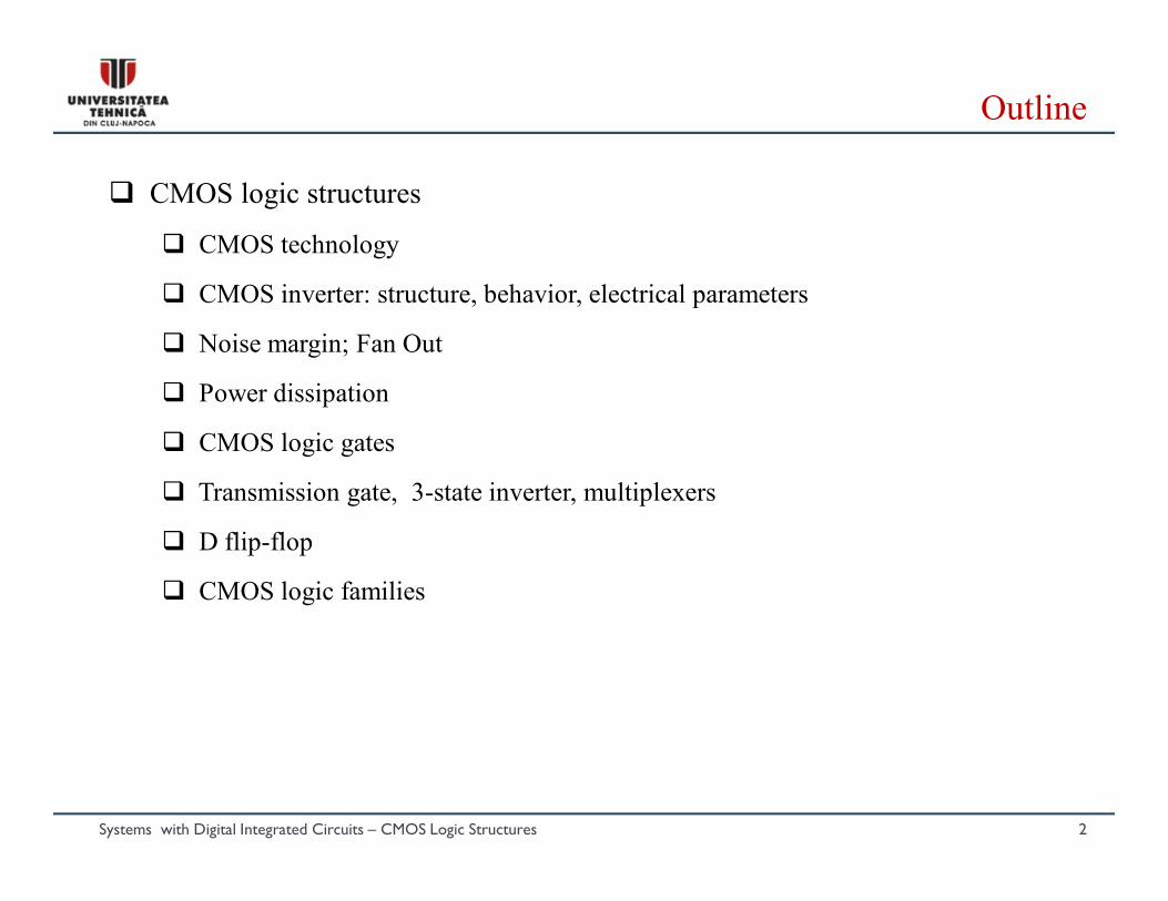
Outline
Systems with Digital Integrated Circuits – CMOS Logic Structures 2
CMOS logic structures
CMOS technology
CMOS inverter: structure, behavior, electrical parameters
Noise margin; Fan Out
Power dissipation
CMOS logic gates
Transmission gate, 3-state inverter, multiplexers
D flip-flop
CMOS logic families
Systems with Digital Integrated Circuits – CMOS Logic Structures 3
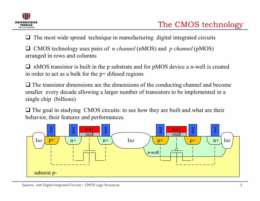
The CMOS technology
The most wide spread technique in manufacturing digital integrated circuits
CMOS technology uses pairs of n channel (nMOS) and p channel (pMOS)
arranged in rows and columns
nMOS transistor is built in the p substrate and for pMOS device a n-well is created
in order to act as a bulk for the p+ difused regions
The transistor dimensions are the dimensions of the conducting channel and become
smaller every decade allowing a larger number of transistors to be implemented in a
single chip (billions)
The goal in studying CMOS circuits: to see how they are built and what are their
behavior, their features and performances.
Systems with Digital Integrated Circuits – CMOS Logic Structures 4
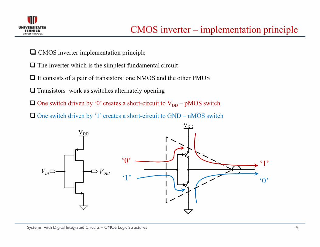
CMOS inverter – implementation principle
CMOS inverter implementation principle
The inverter which is the simplest fundamental circuit
It consists of a pair of transistors: one NMOS and the other PMOS
Transistors work as switches alternately opening
One switch driven by ‘0’ creates a short-circuit to VDD – pMOS switch
One switch driven by ‘1’ creates a short-circuit to GND – nMOS switch
‘0’ ‘1’
‘1’ ‘0’
VDD
VoutVin
Sisteme cu circuite integrate digitale – Structuri logice CMOS 5
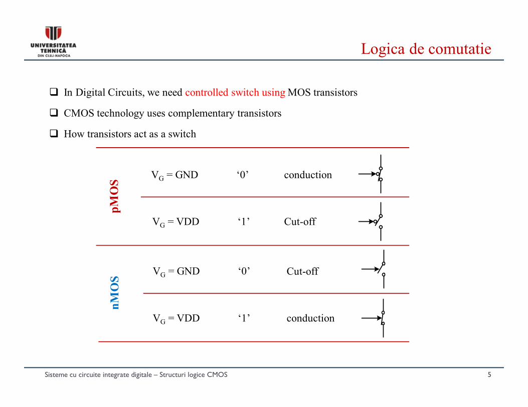
Logica de comutatie
conductionVG = GND
Cut-offVG = VDD
pM
OS
‘0’
‘1’
In Digital Circuits, we need controlled switch using MOS transistors
CMOS technology uses complementary transistors
How transistors act as a switch
Cut-offVG = GND
conductionVG = VDD
nM
OS
‘0’
‘1’
Sisteme cu circuite integrate digitale – Structuri logice CMOS 6
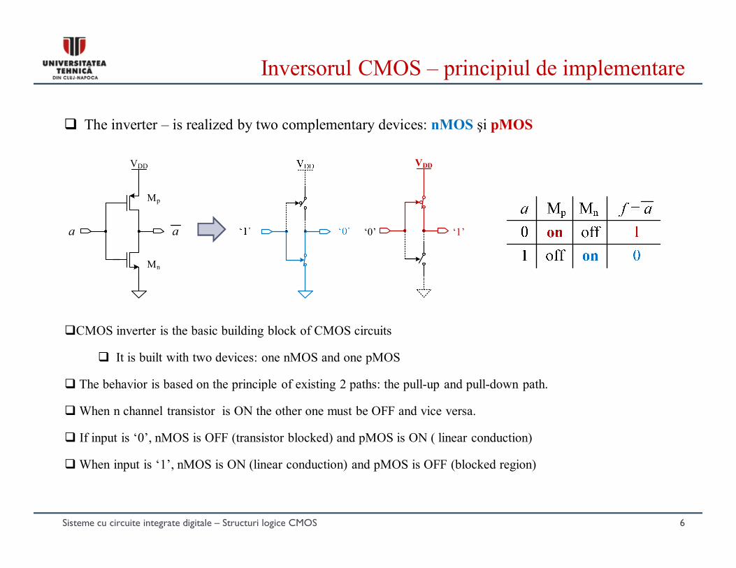
Inversorul CMOS – principiul de implementare
VDD
‘1’‘0’
VDD
aa
Mp
Mn
CMOS inverter is the basic building block of CMOS circuits
It is built with two devices: one nMOS and one pMOS
The behavior is based on the principle of existing 2 paths: the pull-up and pull-down path.
When n channel transistor is ON the other one must be OFF and vice versa.
If input is ‘0’, nMOS is OFF (transistor blocked) and pMOS is ON ( linear conduction)
When input is ‘1’, nMOS is ON (linear conduction) and pMOS is OFF (blocked region)
The inverter – is realized by two complementary devices: nMOS şi pMOS
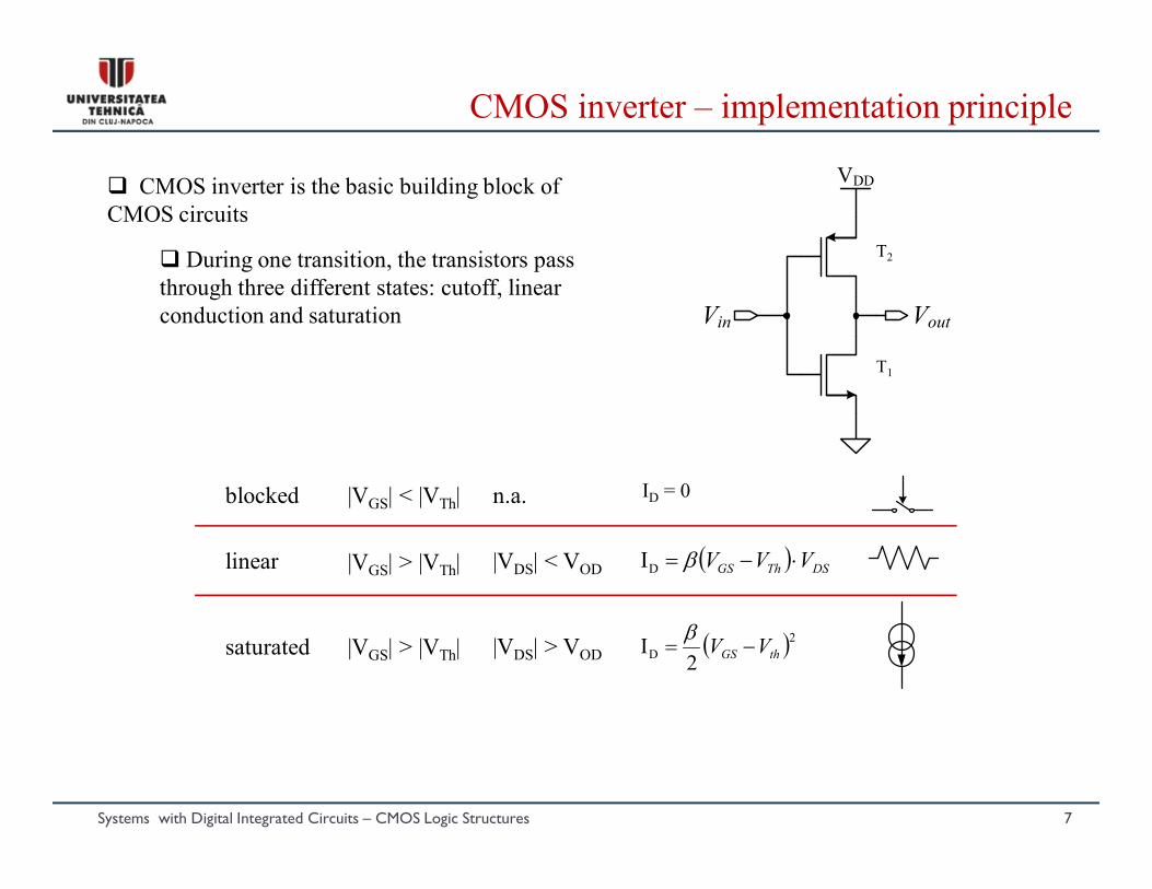
Systems with Digital Integrated Circuits – CMOS Logic Structures 7
CMOS inverter – implementation principle
CMOS inverter is the basic building block of
CMOS circuits
During one transition, the transistors pass
through three different states: cutoff, linear
conduction and saturation
VDD
VoutVin
T2
T1
blocked |VGS| < |VTh| n.a.
linear |VDS| < VOD
saturated
ID = 0
2D2
I thGS VV
DSThGS VVV DI|VGS| > |VTh|
|VGS| > |VTh| |VDS| > VOD
Systems with Digital Integrated Circuits – CMOS Logic Structures 8
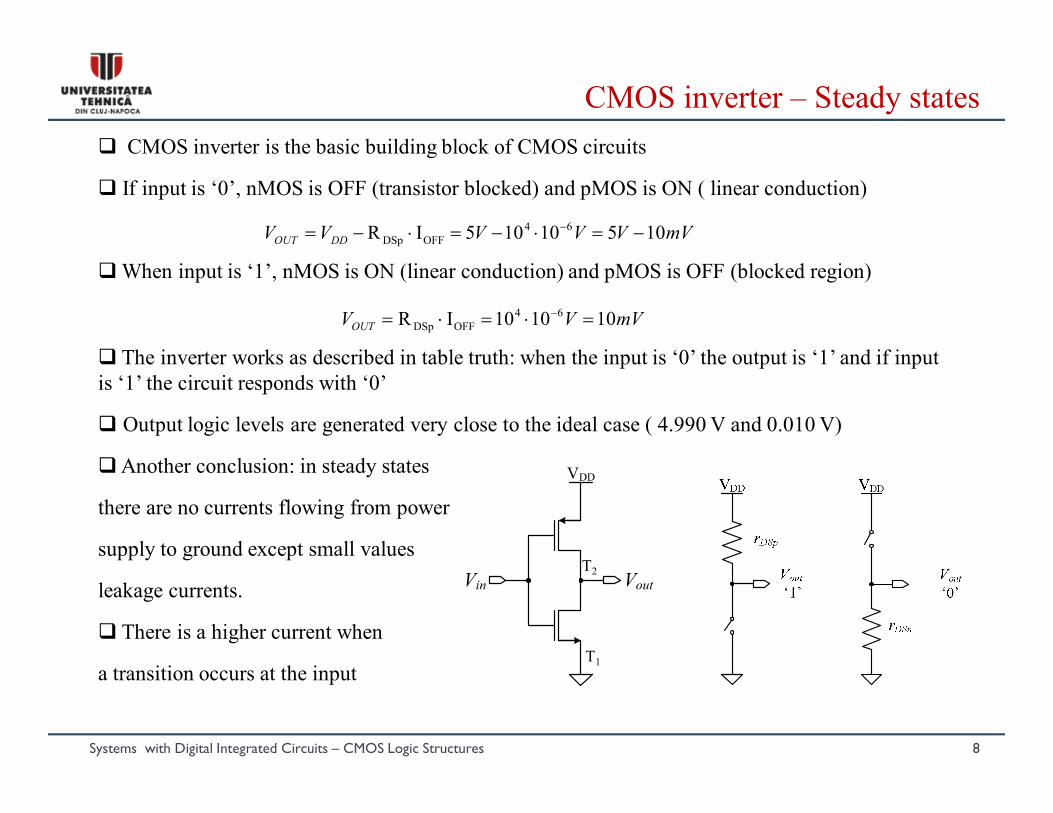
CMOS inverter – Steady states
CMOS inverter is the basic building block of CMOS circuits
If input is ‘0’, nMOS is OFF (transistor blocked) and pMOS is ON ( linear conduction)
When input is ‘1’, nMOS is ON (linear conduction) and pMOS is OFF (blocked region)
The inverter works as described in table truth: when the input is ‘0’ the output is ‘1’ and if input
is ‘1’ the circuit responds with ‘0’
Output logic levels are generated very close to the ideal case ( 4.990 V and 0.010 V)
Another conclusion: in steady states
there are no currents flowing from power
supply to ground except small values
leakage currents.
There is a higher current when
a transition occurs at the input
VDD
VoutVin
T2
T1
mVVVVVV DDOUT 10510105I R 64
OFFDSp
mVVVOUT 101010I R 64
OFFDSp
Systems with Digital Integrated Circuits – CMOS Logic Structures 9
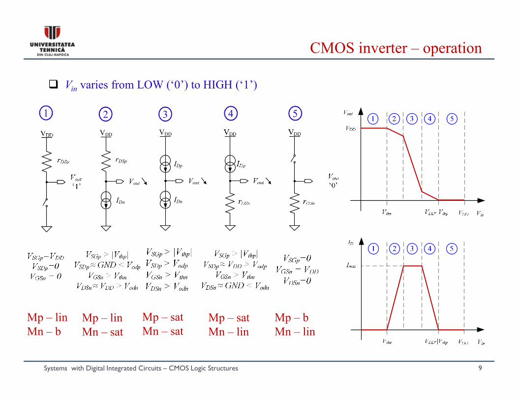
CMOS inverter – operation
Vin varies from LOW (‘0’) to HIGH (‘1’)
VDD
Vout
rDSp
IDn
VDD
Vout
IDn
IDp
Mp – lin
Mn – b
Mp – lin
Mn – sat
Mp – sat
Mn – sat
Mp – sat
Mn – lin
Mp – b
Mn – lin
1 2 3 4 5
Systems with Digital Integrated Circuits – CMOS Logic Structures 10
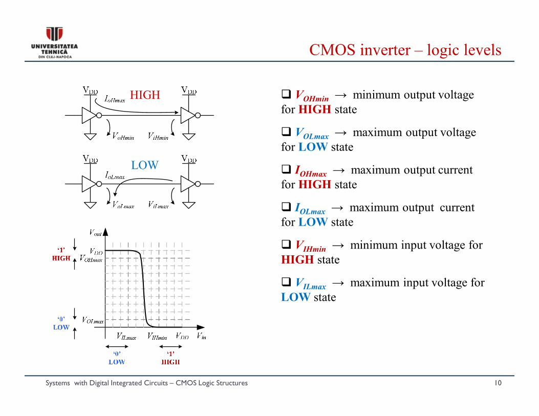
CMOS inverter – logic levels
VOHmin → minimum output voltage
for HIGH state
VOLmax → maximum output voltage
for LOW state
IOHmax → maximum output current
for HIGH state
IOLmax → maximum output current
for LOW state
VIHmin → minimum input voltage for
HIGH state
VILmax → maximum input voltage for
LOW state
HIGH
LOW
Systems with Digital Integrated Circuits – CMOS Logic Structures 11
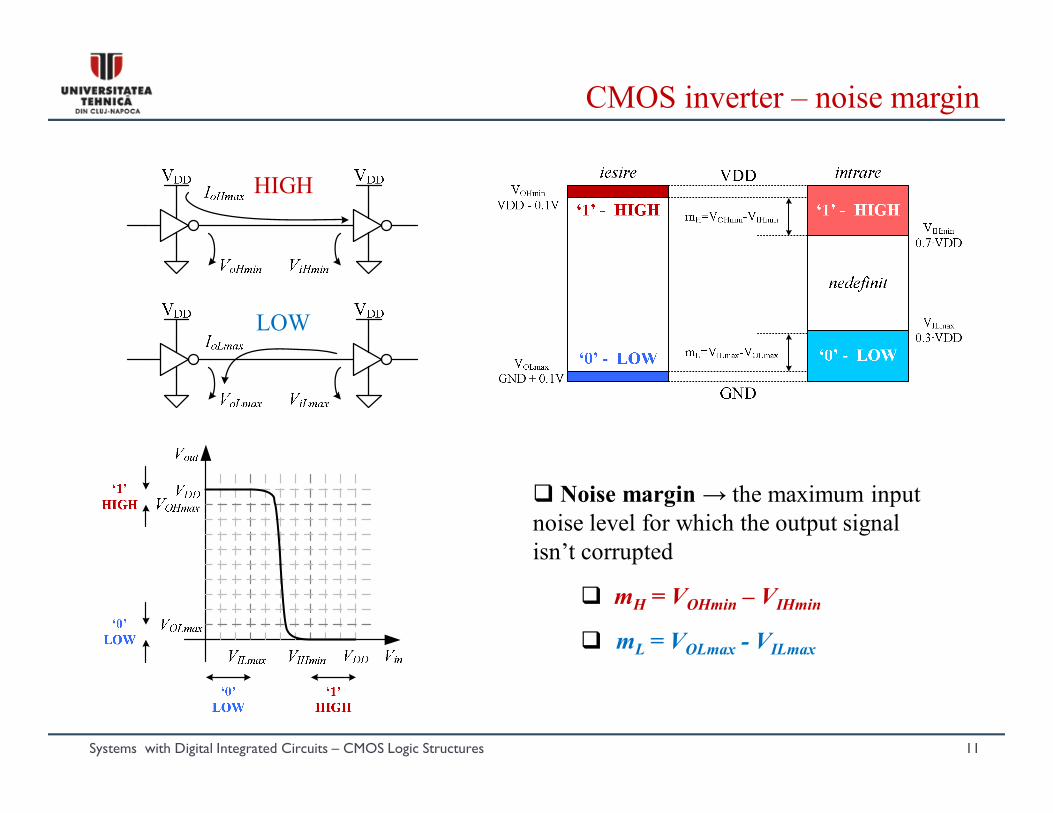
CMOS inverter – noise margin
HIGH
LOW
Noise margin → the maximum input
noise level for which the output signal
isn’t corrupted
mH = VOHmin – VIHmin
mL = VOLmax - VILmax
Systems with Digital Integrated Circuits – CMOS Logic Structures 12
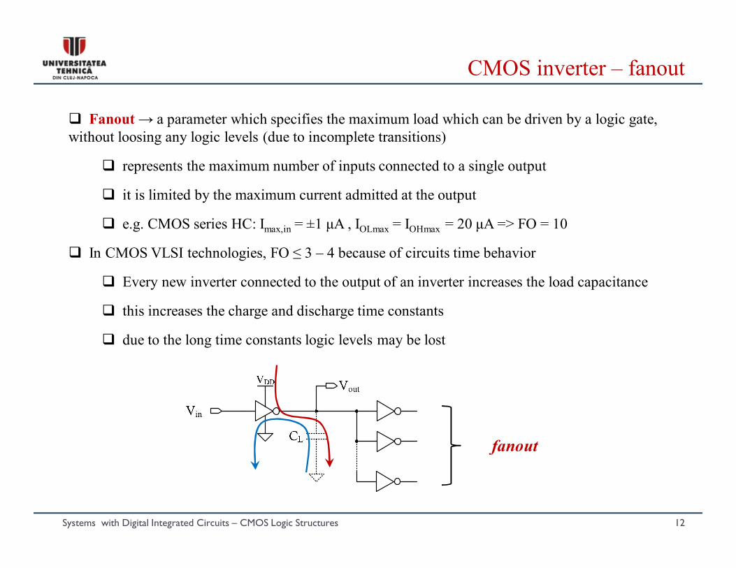
CMOS inverter – fanout
Fanout → a parameter which specifies the maximum load which can be driven by a logic gate,
without loosing any logic levels (due to incomplete transitions)
represents the maximum number of inputs connected to a single output
it is limited by the maximum current admitted at the output
e.g. CMOS series HC: Imax,in = ±1 μA , IOLmax = IOHmax = 20 μA => FO = 10
In CMOS VLSI technologies, FO ≤ 3 – 4 because of circuits time behavior
Every new inverter connected to the output of an inverter increases the load capacitance
this increases the charge and discharge time constants
due to the long time constants logic levels may be lost
fanout
Systems with Digital Integrated Circuits – CMOS Logic Structures 13
CMOS inverter – power consumption
The power consumption determines the consumption of energy from the supply rails
and causes heat dissipation
Knowledge of this parameter is important in order to determine the capacity of the
supply source, the battery lifetime, sizing the supply rails, the packaging and the way of
cooling the package
The power consumption consists of three components:
Pstat – static power dissipated due to the current which flows during the static
operation
Pdyn – dynamic power dissipated during the charging and discharging of the load
capacitance
Pdp – dynamic power dissipated due to the simultaneous conduction of the
nMOS and pMOS transistors
dpdynstattot PPPP
Systems with Digital Integrated Circuits – CMOS Logic Structures 14
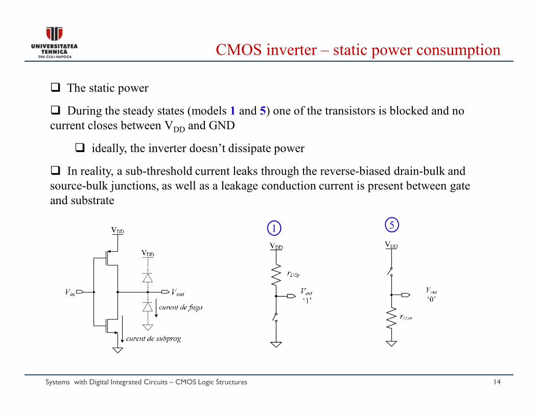
CMOS inverter – static power consumption
The static power
During the steady states (models 1 and 5) one of the transistors is blocked and no
current closes between VDD and GND
ideally, the inverter doesn’t dissipate power
In reality, a sub-threshold current leaks through the reverse-biased drain-bulk and
source-bulk junctions, as well as a leakage conduction current is present between gate
and substrate
1 5
Systems with Digital Integrated Circuits – CMOS Logic Structures 15
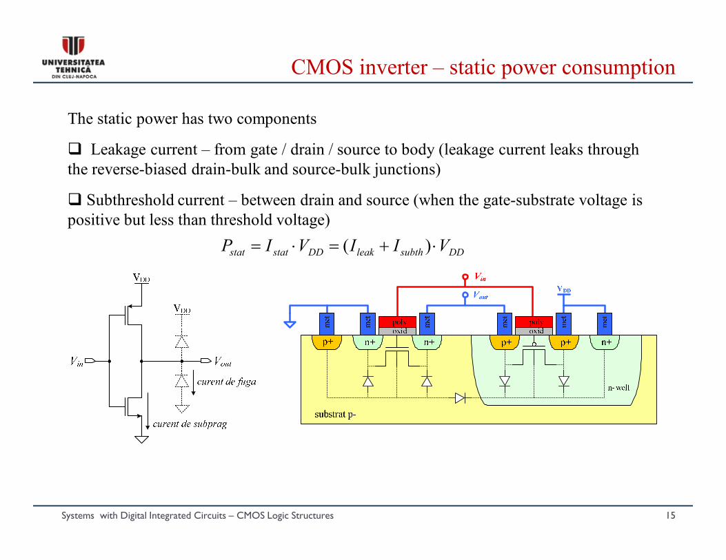
CMOS inverter – static power consumption
The static power has two components
Leakage current – from gate / drain / source to body (leakage current leaks through
the reverse-biased drain-bulk and source-bulk junctions)
Subthreshold current – between drain and source (when the gate-substrate voltage is
positive but less than threshold voltage)
DDsubthleakDDstatstat VIIVIP )(
Systems with Digital Integrated Circuits – CMOS Logic Structures 16
CMOS inverter – static power consumption
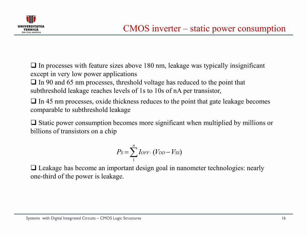
In processes with feature sizes above 180 nm, leakage was typically insignificant
except in very low power applications
In 90 and 65 nm processes, threshold voltage has reduced to the point that
subthreshold leakage reaches levels of 1s to 10s of nA per transistor,
In 45 nm processes, oxide thickness reduces to the point that gate leakage becomes
comparable to subthreshold leakage
Static power consumption becomes more significant when multiplied by millions or
billions of transistors on a chip
Leakage has become an important design goal in nanometer technologies: nearly
one-third of the power is leakage.
n
SSDDOFFS VVIP1
)(
Systems with Digital Integrated Circuits – CMOS Logic Structures 17
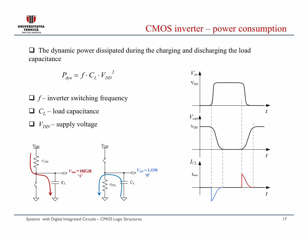
CMOS inverter – power consumption
The dynamic power dissipated during the charging and discharging the load
capacitance
f – inverter switching frequency
CL – load capacitance
VDD – supply voltage
2
DDLdyn VCfP
Systems with Digital Integrated Circuits – CMOS Logic Structures 18
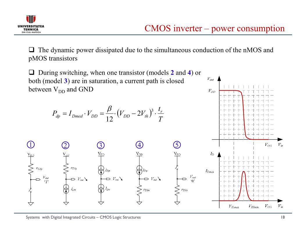
CMOS inverter – power consumption
The dynamic power dissipated due to the simultaneous conduction of the nMOS and
pMOS transistors
1 2 3 4 5
During switching, when one transistor (models 2 and 4) or
both (model 3) are in saturation, a current path is closed
between VDD and GND
T
tVVVIP r
thDDDDDmeddp 3
212
Systems with Digital Integrated Circuits – CMOS Logic Structures 19
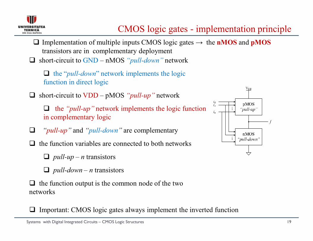
CMOS logic gates - implementation principle
Implementation of multiple inputs CMOS logic gates → the nMOS and pMOS
transistors are in complementary deployment
short-circuit to GND – nMOS “pull-down” network
the “pull-down” network implements the logic
function in direct logic
short-circuit to VDD – pMOS “pull-up” network
the “pull-up” network implements the logic function
in complementary logic
“pull-up” and “pull-down” are complementary
the function variables are connected to both networks
pull-up – n transistors
pull-down – n transistors
the function output is the common node of the two
networks
Important: CMOS logic gates always implement the inverted function
Systems with Digital Integrated Circuits – CMOS Logic Structures 20
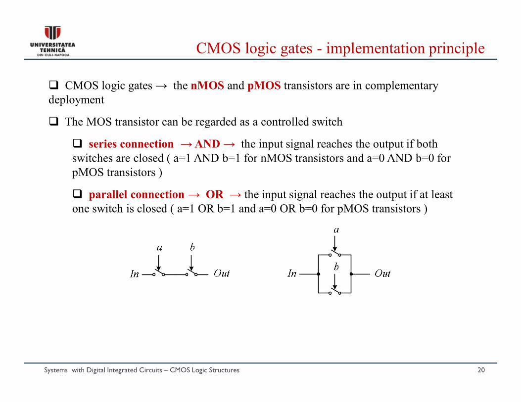
CMOS logic gates - implementation principle
CMOS logic gates → the nMOS and pMOS transistors are in complementary
deployment
The MOS transistor can be regarded as a controlled switch
series connection → AND → the input signal reaches the output if both
switches are closed ( a=1 AND b=1 for nMOS transistors and a=0 AND b=0 for
pMOS transistors )
parallel connection → OR → the input signal reaches the output if at least
one switch is closed ( a=1 OR b=1 and a=0 OR b=0 for pMOS transistors )
Systems with Digital Integrated Circuits – CMOS Logic Structures 21
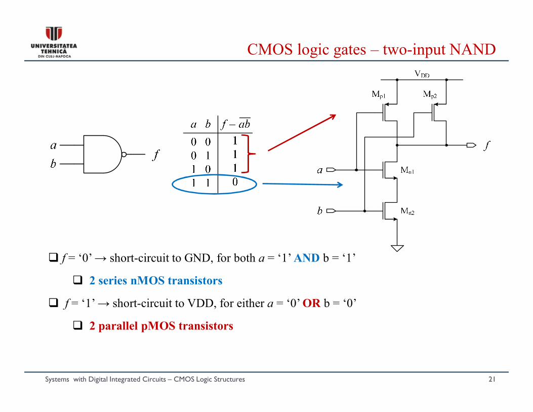
CMOS logic gates – two-input NAND
f = ‘0’ → short-circuit to GND, for both a = ‘1’ AND b = ‘1’
2 series nMOS transistors
f = ‘1’ → short-circuit to VDD, for either a = ‘0’ OR b = ‘0’
2 parallel pMOS transistors
Systems with Digital Integrated Circuits – CMOS Logic Structures 22
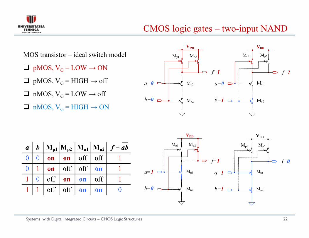
CMOS logic gates – two-input NAND
MOS transistor – ideal switch model
pMOS, VG = LOW → ON
pMOS, VG = HIGH → off
nMOS, VG = LOW → off
nMOS, VG = HIGH → ON
f=1
a=1
b=0
VDD
Mp1 Mp2
Mn1
Mn2
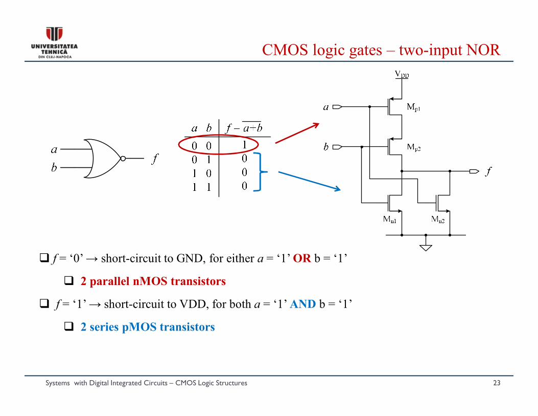
Systems with Digital Integrated Circuits – CMOS Logic Structures 23
CMOS logic gates – two-input NOR
f = ‘0’ → short-circuit to GND, for either a = ‘1’ OR b = ‘1’
2 parallel nMOS transistors
f = ‘1’ → short-circuit to VDD, for both a = ‘1’ AND b = ‘1’
2 series pMOS transistors
Systems with Digital Integrated Circuits – CMOS Logic Structures 24
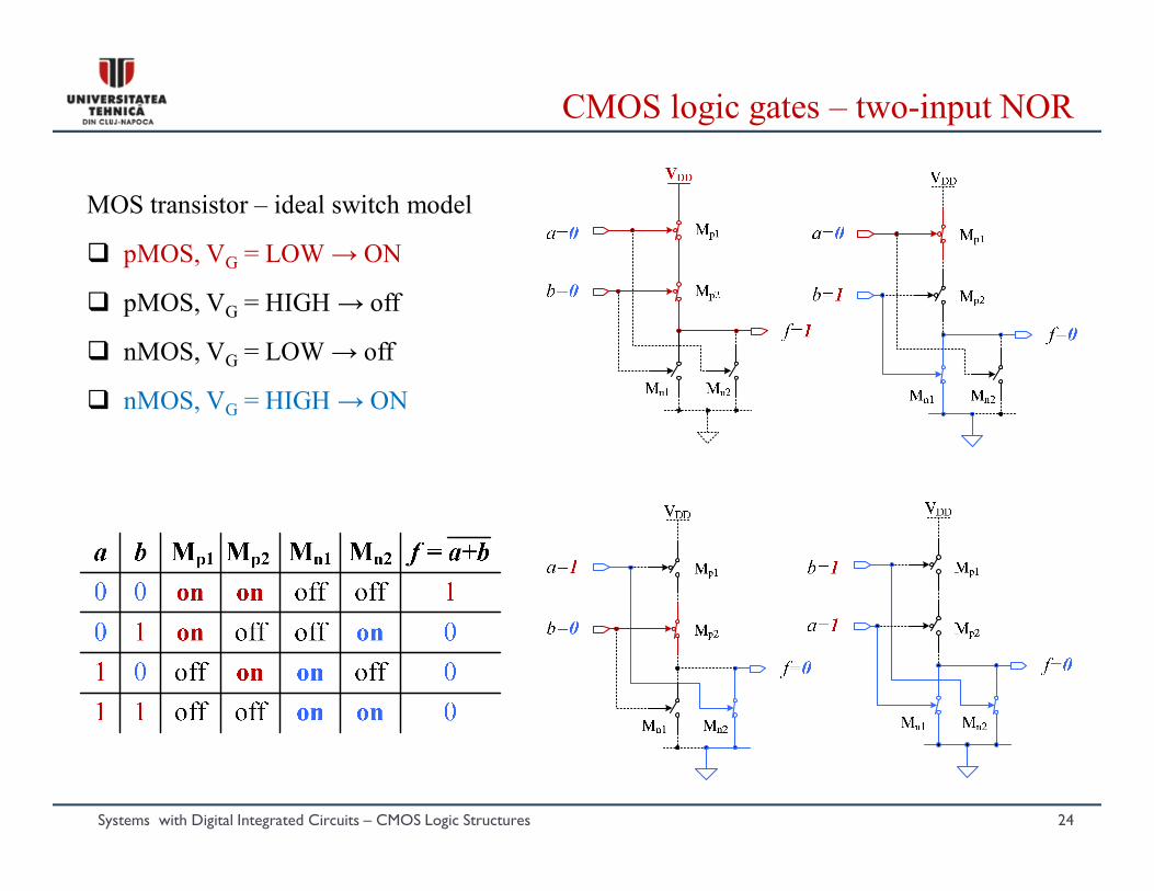
CMOS logic gates – two-input NOR
MOS transistor – ideal switch model
pMOS, VG = LOW → ON
pMOS, VG = HIGH → off
nMOS, VG = LOW → off
nMOS, VG = HIGH → ON
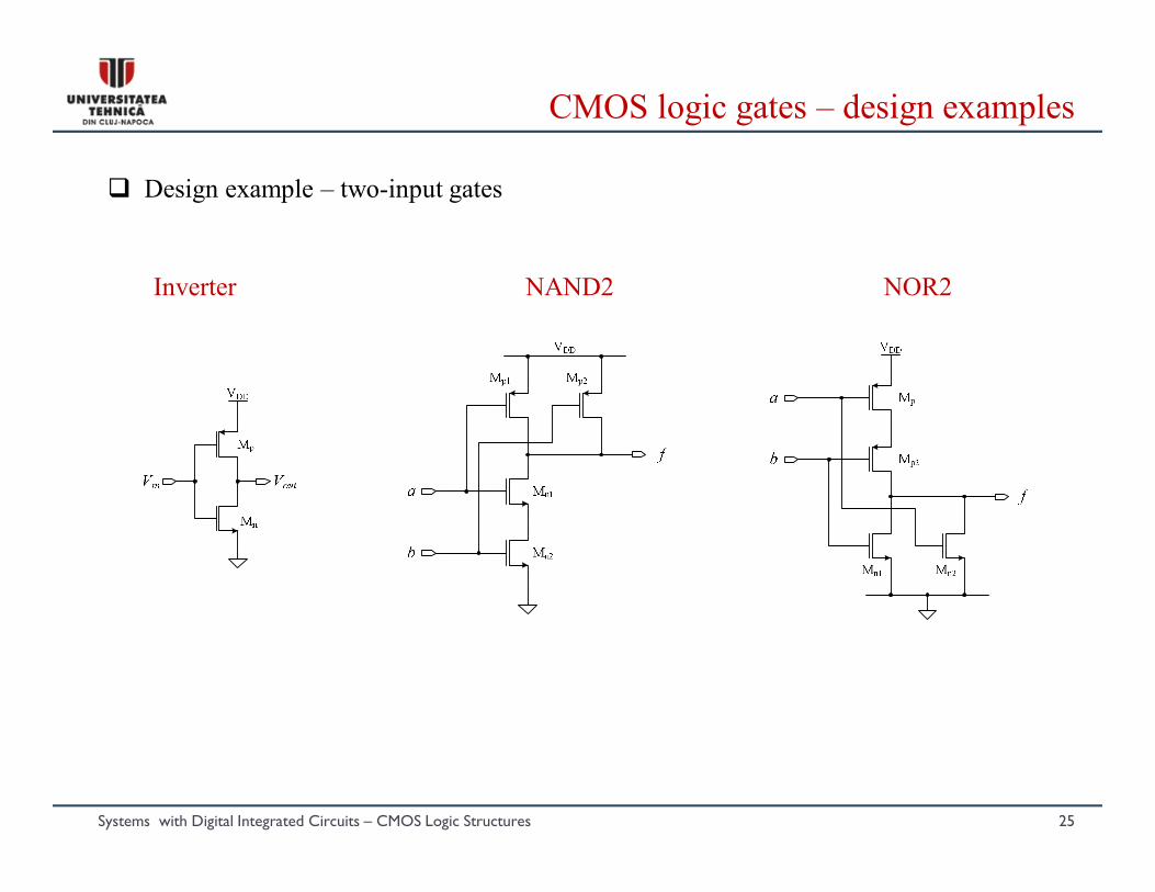
Design example – two-input gates
Inverter NAND2 NOR2
Systems with Digital Integrated Circuits – CMOS Logic Structures 25
CMOS logic gates – design examples
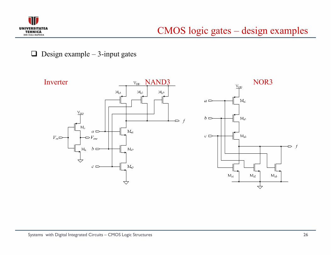
Design example – 3-input gates
Inverter NAND3 NOR3
Systems with Digital Integrated Circuits – CMOS Logic Structures 26
CMOS logic gates – design examples
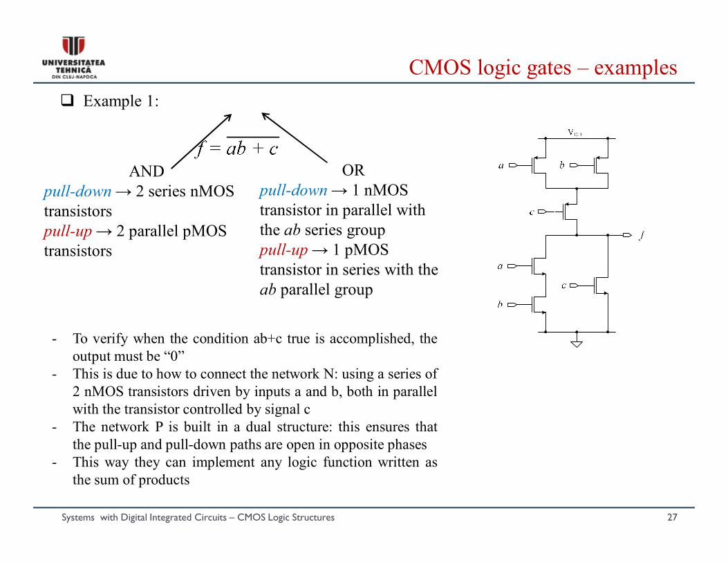
Systems with Digital Integrated Circuits – CMOS Logic Structures 27
CMOS logic gates – examples
AND
pull-down → 2 series nMOS
transistors
pull-up → 2 parallel pMOS
transistors
OR
pull-down → 1 nMOS
transistor in parallel with
the ab series group
pull-up → 1 pMOS
transistor in series with the
ab parallel group
Example 1:
- To verify when the condition ab+c true is accomplished, the
output must be “0”
- This is due to how to connect the network N: using a series of
2 nMOS transistors driven by inputs a and b, both in parallel
with the transistor controlled by signal c
- The network P is built in a dual structure: this ensures that
the pull-up and pull-down paths are open in opposite phases
- This way they can implement any logic function written as
the sum of products
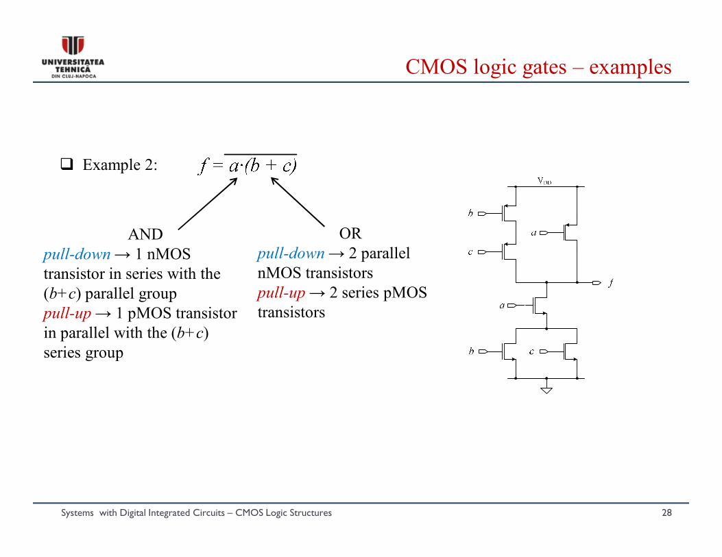
Systems with Digital Integrated Circuits – CMOS Logic Structures 28
CMOS logic gates – examples
AND
pull-down → 1 nMOS
transistor in series with the
(b+c) parallel group
pull-up → 1 pMOS transistor
in parallel with the (b+c)
series group
OR
pull-down → 2 parallel
nMOS transistors
pull-up → 2 series pMOS
transistors
Example 2:
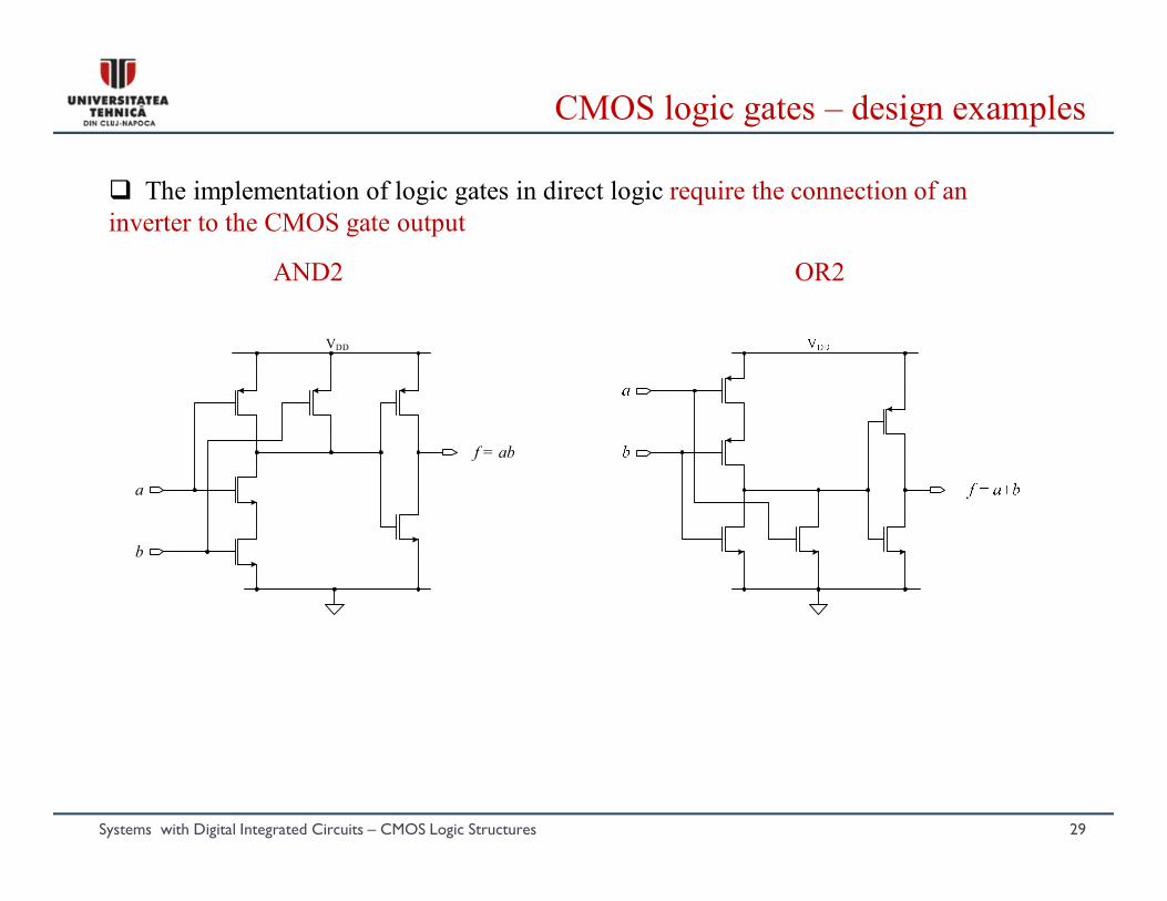
The implementation of logic gates in direct logic require the connection of an
inverter to the CMOS gate output
AND2 OR2
Systems with Digital Integrated Circuits – CMOS Logic Structures 29
CMOS logic gates – design examples
VDD
a
b
f = ab
Systems with Digital Integrated Circuits – CMOS Logic Structures 30
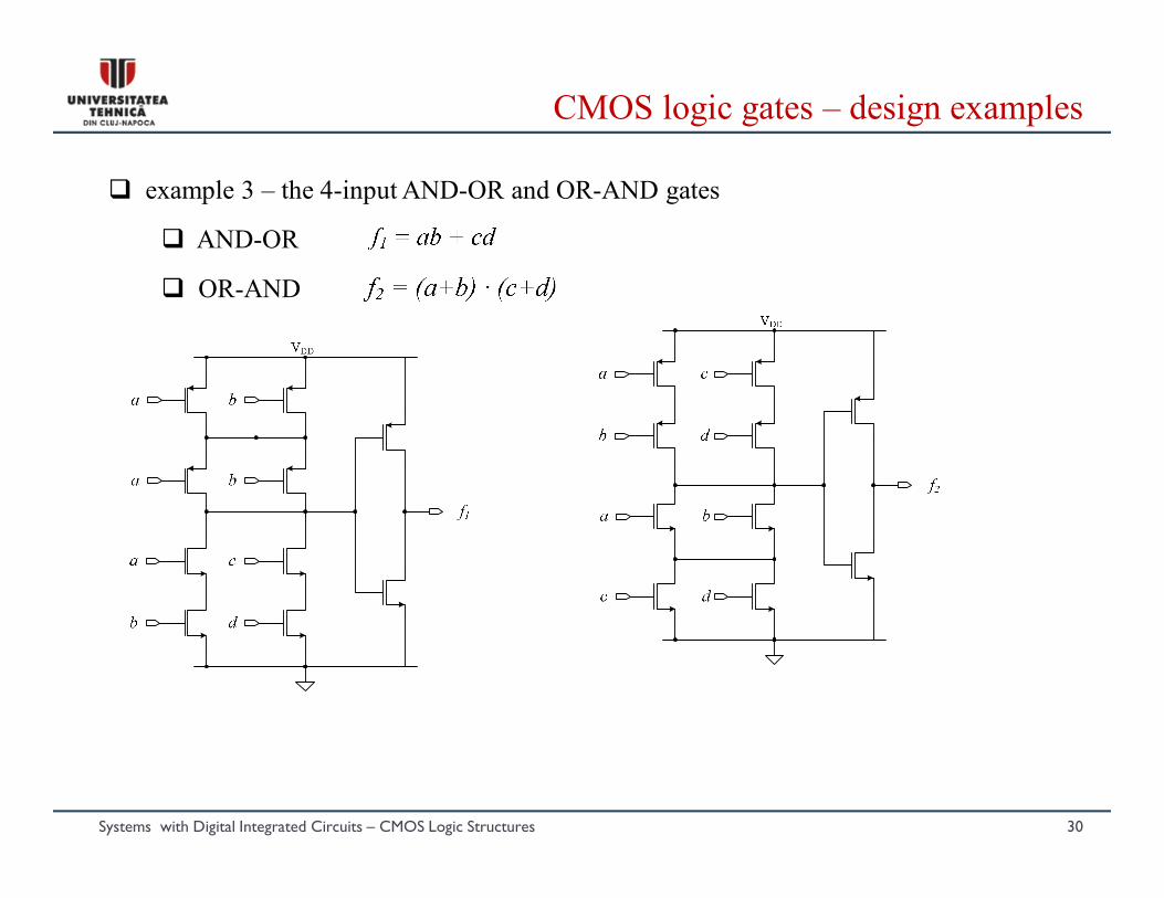
CMOS logic gates – design examples
example 3 – the 4-input AND-OR and OR-AND gates
AND-OR
OR-AND
Systems with Digital Integrated Circuits – CMOS Logic Structures 31
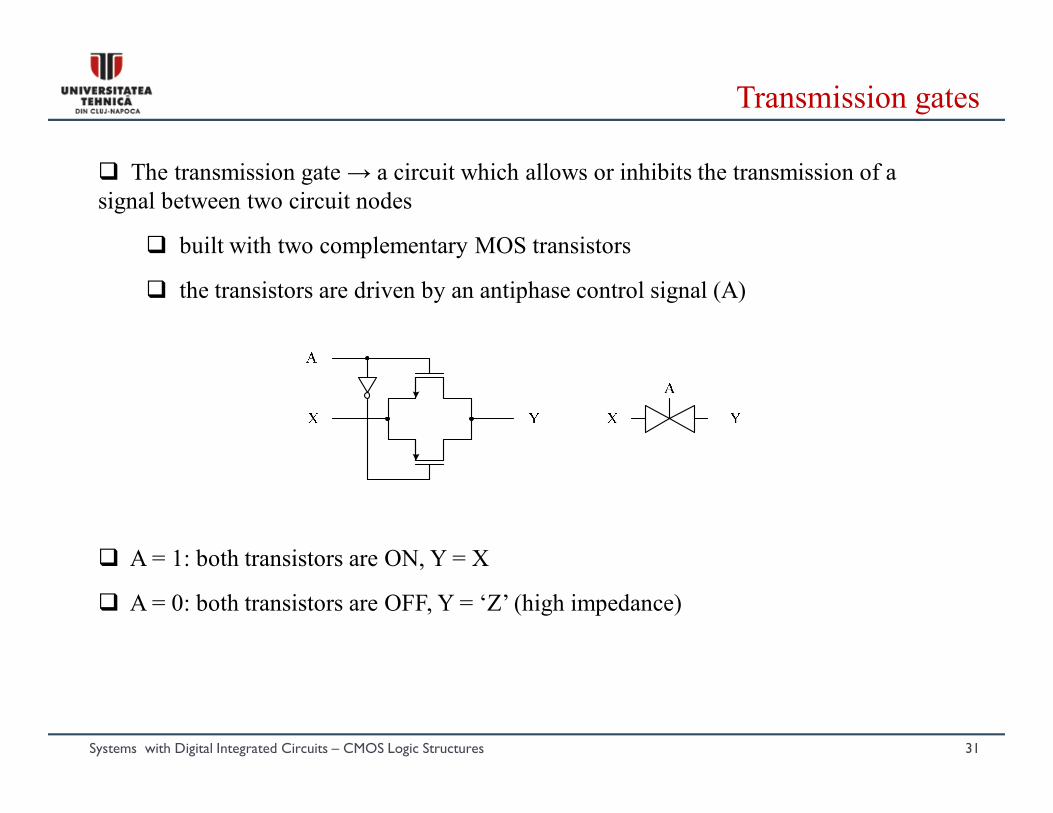
Transmission gates
The transmission gate → a circuit which allows or inhibits the transmission of a
signal between two circuit nodes
built with two complementary MOS transistors
the transistors are driven by an antiphase control signal (A)
A = 1: both transistors are ON, Y = X
A = 0: both transistors are OFF, Y = ‘Z’ (high impedance)
Sisteme cu circuite integrate digitale – Structuri logice CMOS 32
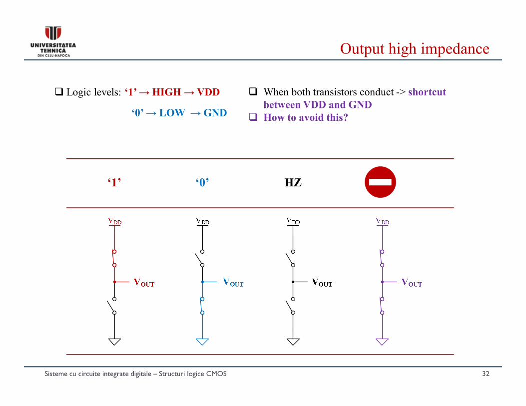
Output high impedance
Logic levels: ‘1’ → HIGH → VDD
‘0’ → LOW → GND
‘1’ ‘0’ HZ
When both transistors conduct -> shortcut
between VDD and GND
How to avoid this?
Systems with Digital Integrated Circuits – CMOS Logic Structures 33
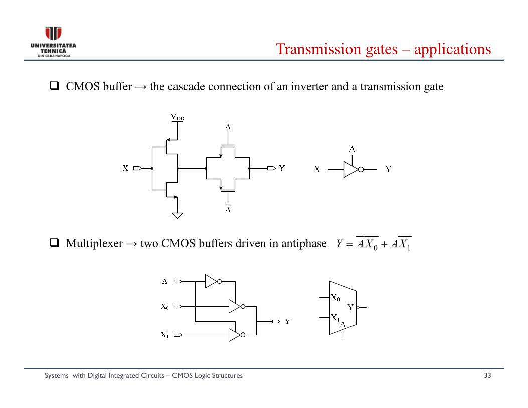
Transmission gates – applications
CMOS buffer → the cascade connection of an inverter and a transmission gate
Multiplexer → two CMOS buffers driven in antiphase 10 XAXAY
Systems with Digital Integrated Circuits – CMOS Logic Structures 34
Transmission gates – applications
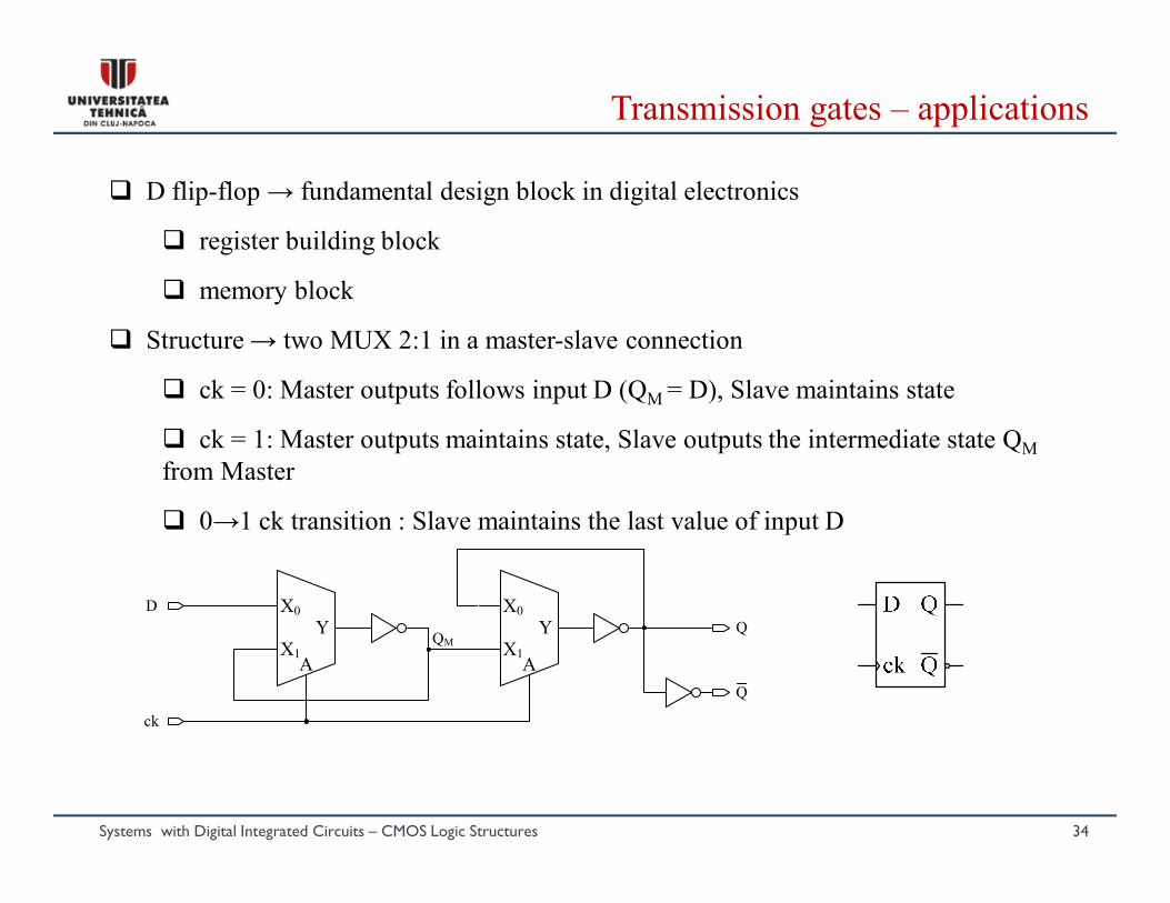
D flip-flop → fundamental design block in digital electronics
register building block
memory block
Structure → two MUX 2:1 in a master-slave connection
ck = 0: Master outputs follows input D (QM = D), Slave maintains state
ck = 1: Master outputs maintains state, Slave outputs the intermediate state QM
from Master
0→1 ck transition : Slave maintains the last value of input D
X0
X1A
YX0
X1A
Y
D
ck
Q
Q
QM
Systems with Digital Integrated Circuits – CMOS Logic Structures 35
CMOS logic circuit design objectives
Ideal gate: fast and low-power
Digital system design must follow an increased operation speed, low power
consumption and small circuit area
Power-delay product (PDP) → is defined as a quality measure for the logic circuits
which operate based on switching, and is the product between the time delay and power
consumption
PDP is constant for a given technology and circuit topology:
for smaller propagation delay, the transistors are redesigned by increasing the
channel widths
the transistor area is increased, leading to the increase of the drain current, and
therefore the power consumption
the product of the two values (PDP) stays constant
Systems with Digital Integrated Circuits – CMOS Logic Structures 36
CMOS logic families
CMOS 4000 – the first CMOS family
simple structure of the fundamental gates
low power consumption
slow operation speed
difficult interfacing with TTL circuits
CMOS HC (High Speed CMOS) and HCT (TTL Compatible)
high speed, TTL compatibility: 74LLLnnn (74 – Texas Instruments codes in the
commercial range, 54 – military range, nnn – circuit function, LLL - family)
CMOS VHC (Very High Speed), VHCT (TTL Compatible)
double operation frequency compared to former generations
CMOS FCT (Fast CMOS, TTL Compatible)
CMOS FCT-T (with TTL VOH)
as fast as TTL, low-power and TTL compatible (VOH<5V, compatible to the HIGH TTL
level)
Systems with Digital Integrated Circuits – CMOS Logic Structures 37
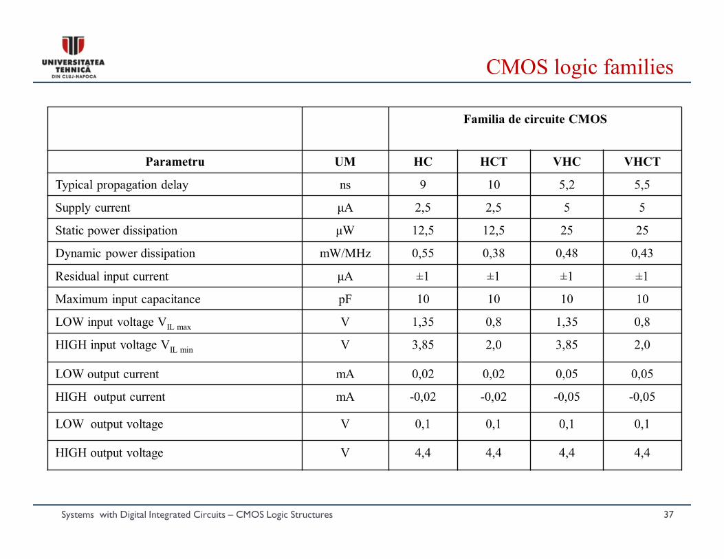
CMOS logic families
Familia de circuite CMOS
Parametru UM HC HCT VHC VHCT
Typical propagation delay ns 9 10 5,2 5,5
Supply current μA 2,5 2,5 5 5
Static power dissipation μW 12,5 12,5 25 25
Dynamic power dissipation mW/MHz 0,55 0,38 0,48 0,43
Residual input current μA ±1 ±1 ±1 ±1
Maximum input capacitance pF 10 10 10 10
LOW input voltage VIL max V 1,35 0,8 1,35 0,8
HIGH input voltage VIL min V 3,85 2,0 3,85 2,0
LOW output current mA 0,02 0,02 0,05 0,05
HIGH output current mA -0,02 -0,02 -0,05 -0,05
LOW output voltage V 0,1 0,1 0,1 0,1
HIGH output voltage V 4,4 4,4 4,4 4,4
Systems with Digital Integrated Circuits – CMOS Logic Structures 38
References
J. Wakerly – Digital Design, Principle & Practices, Prentice Hall, 1999
Rabaey J.M., Chandrakasan A., Nikolic B. Digital Integrated Circuits. A design perspective.
Prentice Hall, 2003.
Weste N.H.E, Harris D. CMOS VLSI Design. A Circuits and Systems Perspective. Pearson
Addison Wesley, 2005. http://www3.hmc.edu/~harris/cmosvlsi/4e/
H. Kaeslin, “Digital Integrated Circuit Design From VLSI Architecture to CMOS Fabrication”,
Cambridge University Press, 2008.
C. H. Roth, L.K. John, “Digital System Design using VHDL”, Cengage Learning, 2008.
Willy M. C. Sansen – Analog Design Essentials, Springer, 2006
Ercegovac, M., Lang T., Moreno J. Introduction to Digital Systems. John Wiley &Sons Inc,
New-York, 1999
Sorin Hintea, Mihaela Cirlugea, Lelia Festila. Circuite Integrate Digitale. Editura UT Press,
Cluj-Napoca, 2005
Sorin Hintea. Tehnici de proiectare a circuitelor digitale VLSI. Casa Cartii de Stiinta. Cluj-
Napoca, 1998