Embed Size (px)
Citation preview
2008 BBN Quantum Computing Kickoff
Quantum Materials
David P. Pappas
Jeffrey S. Kline, Minhyea LeeNational Institute of Standards & Technology,
Electronics & Electrical Engineering Laboratory, Boulder, CO
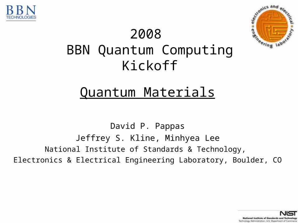
Conventional superconducting circuitMaterials perspective
tunnel barrier
insulator
wiring
substrate
Substrate Si/SiOX Thermal
Wiring Nb or Al Sputtered
Insulator SiOX CVD
Barrier AlOX Thermal
Traditional
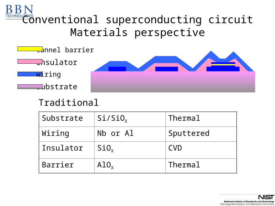
Conventional materials are usedfor a lot of really good reasons…
• Si substrate with thermal a-SiOX on top
– Smooth, standard lithography, inexpensive
• Nb or Al wiring – sputter deposit, polycrystalline
– Low temperature, smooth, relatively high TC
• a-SiOX insulators – CVD
– Smooth (no pinholes), low T, easy
• a-AlOX tunnel barrier – thermal or plasma oxidation
– Smooth, no pinholes, low T, easy, self-limiting“CMOS compatible”
Need strong motivations for change …
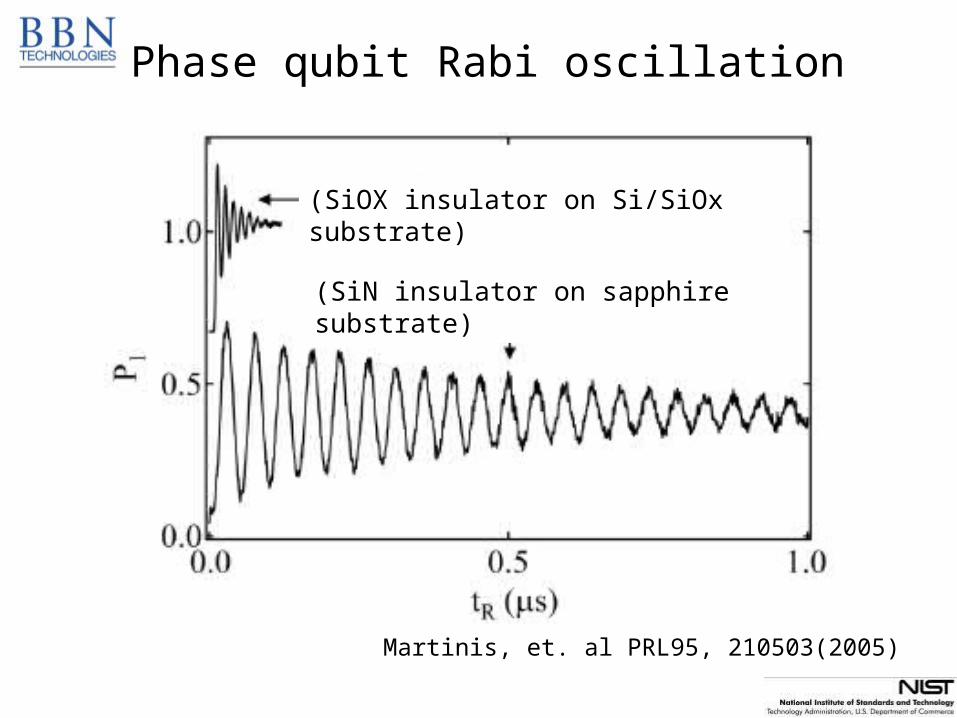
Phase qubit Rabi oscillation
Martinis, et. al PRL95, 210503(2005)
(SiOX insulator on Si/SiOx substrate)
(SiN insulator on sapphire substrate)
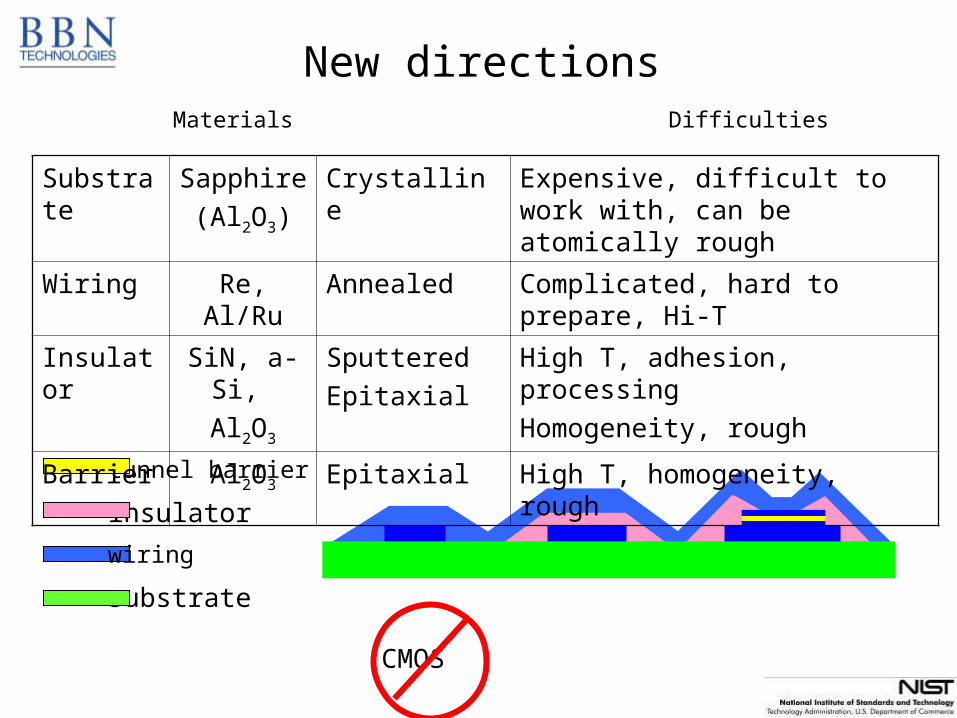
New directions
tunnel barrier
insulator
wiring
substrate
Substrate Sapphire
(Al2O3)
Crystalline Expensive, difficult to work with, can be atomically rough
Wiring Re, Al/Ru Annealed Complicated, hard to prepare, Hi-T
Insulator SiN, a-Si,
Al2O3
Sputtered
Epitaxial
High T, adhesion, processing
Homogeneity, rough
Barrier Al2O3 Epitaxial High T, homogeneity, rough
Materials Difficulties
CMOS
Outline
• Motivations for change
– a-SiOX in substrate & insulators
– a AlOX in barriers
– Superconducting wiring materials
• Milestones & goals
• Recent progress
• Roadmap
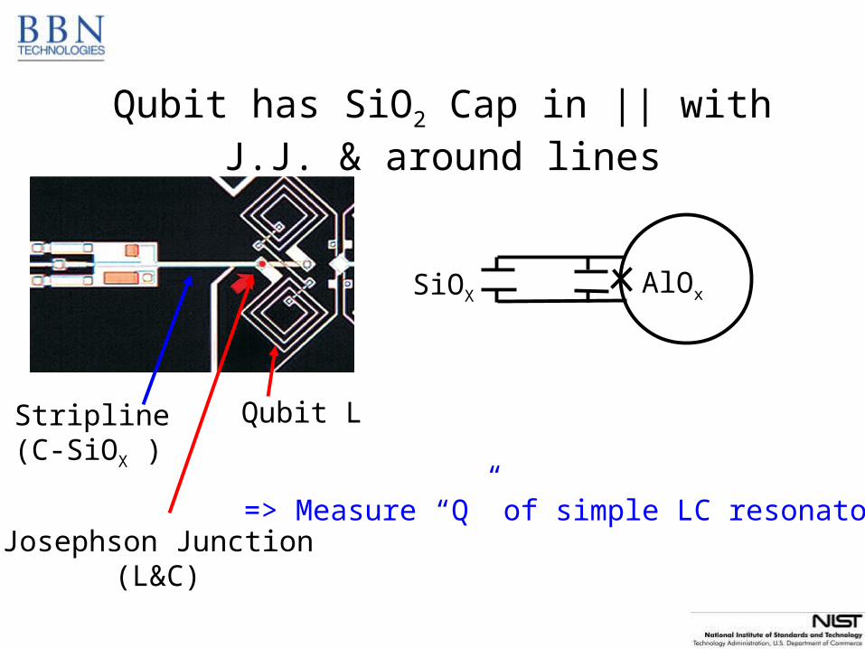
Insert qubit pic here
Qubit LStripline (C-SiOX )
Josephson Junction(L&C)
=> Measure “Q” of simple LC resonators
Qubit has SiO2 Cap in || with J.J. & around lines
SiOX AlOx
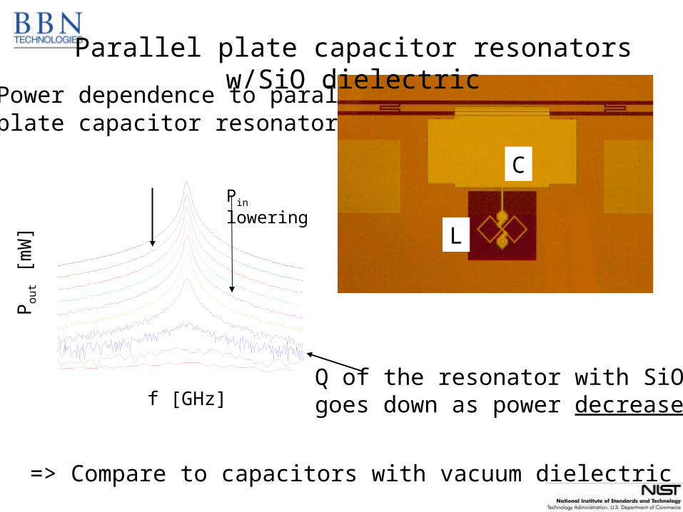
Power dependence to parallelplate capacitor resonators
wave resonator
L
f [GHz]
Po
ut [m
W]
Pin lowering
Q of the resonator with SiO2
goes down as power decreases!
Parallel plate capacitor resonators w/SiO dielectric
C
L
=> Compare to capacitors with vacuum dielectric
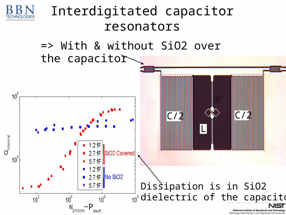
=> With & without SiO2 over the capacitor
C/2 C/2
L
Dissipation is in SiO2dielectric of the capacitor!
~Pout
Interdigitated capacitor resonators
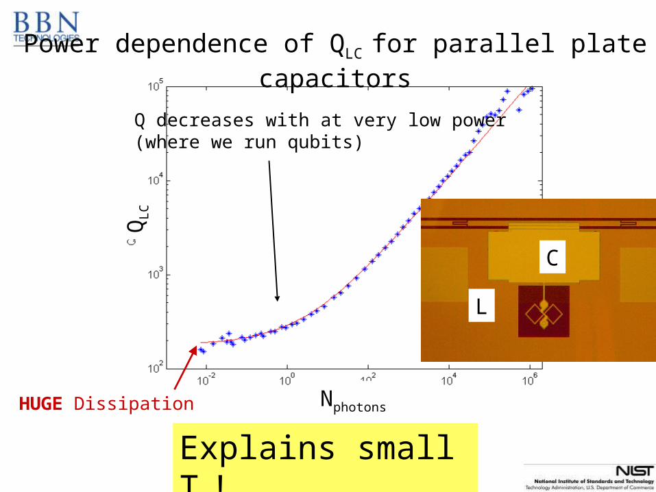
Power dependence of QLC for parallel plate capacitors
HUGE Dissipation
Q decreases with at very low power(where we run qubits)
Nphotons
QL
C
Explains small T1!
L
C
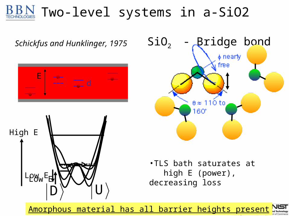
•TLS bath saturates at high E (power), decreasing loss
Schickfus and Hunklinger, 1975
Two-level systems in a-SiO2
E d
SiO2 - Bridge bond
UDAmorphous material has all barrier heights present
High E
Low ELow E
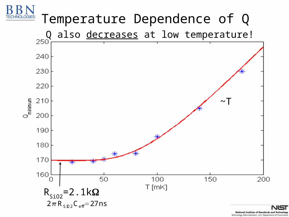
2 RSiO2Ceff 27ns
~T
RSiO2
=2.1k
Temperature Dependence of QQ also decreases at low temperature!
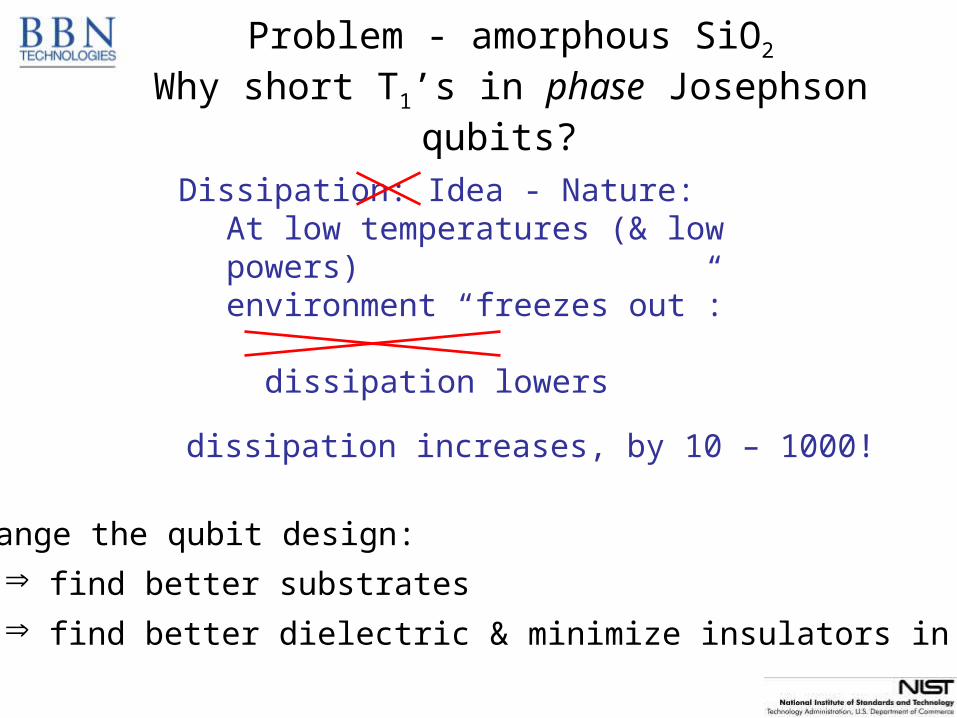
Problem - amorphous SiO2
Why short T1’s in phase Josephson qubits?
Dissipation: Idea - Nature:At low temperatures (& low powers)environment “freezes out”:
dissipation lowers
dissipation increases, by 10 – 1000!
Change the qubit design:
find better substrates
find better dielectric & minimize insulators in design
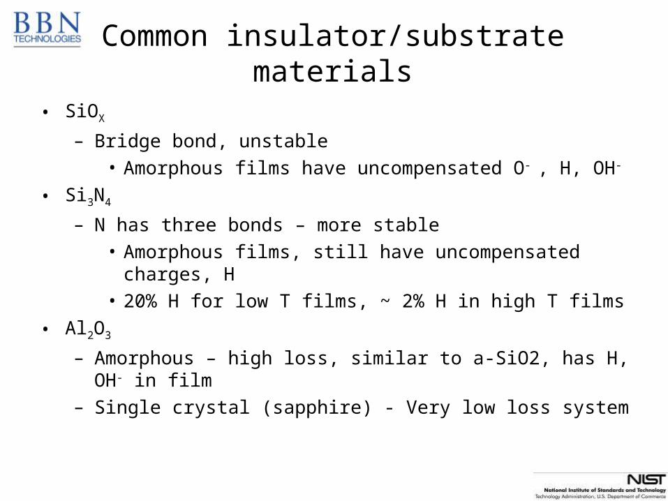
Common insulator/substrate materials
• SiOX
– Bridge bond, unstable• Amorphous films have uncompensated O- , H, OH-
• Si3N4
– N has three bonds – more stable• Amorphous films, still have uncompensated charges, H• 20% H for low T films, ~ 2% H in high T films
• Al2O3
– Amorphous – high loss, similar to a-SiO2, has H, OH- in film– Single crystal (sapphire) - Very low loss system
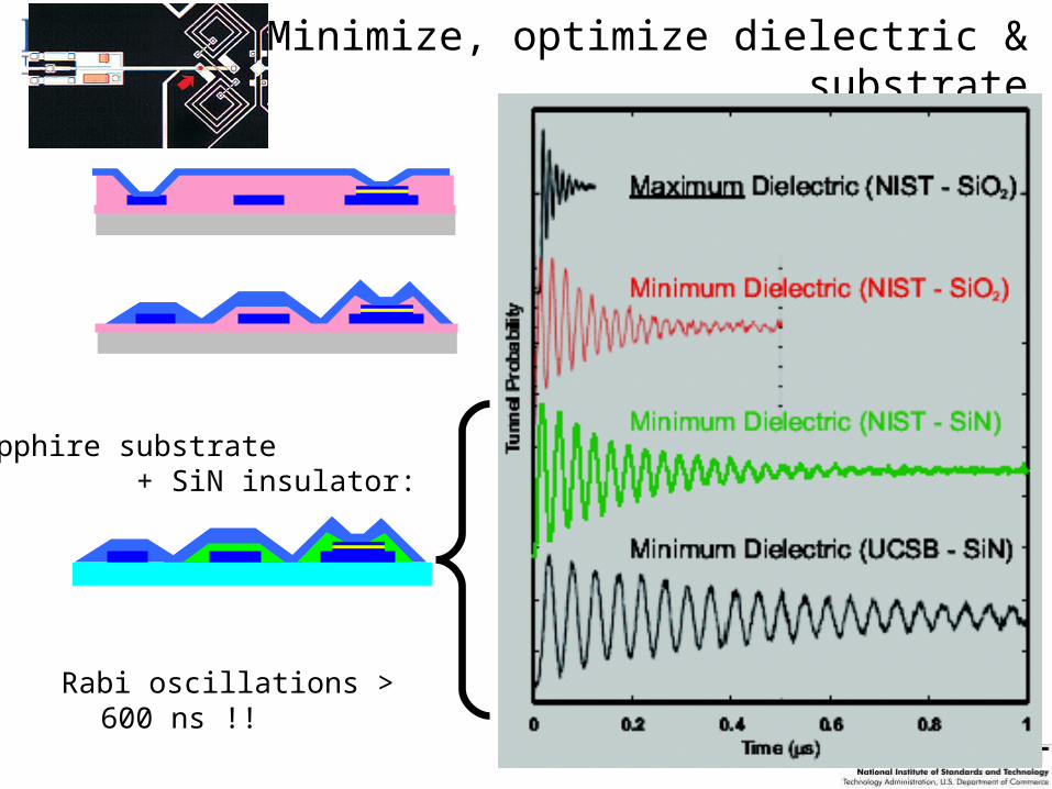
Minimize, optimize dielectric & substrate
Rabi oscillations > 600 ns !!
Sapphire substrate + SiN insulator:
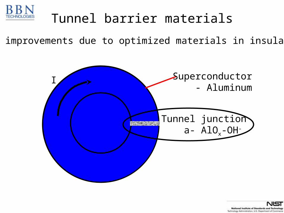
Superconductor - Aluminum
I
Tunnel junction a- AlOx-OH-
Found improvements due to optimized materials in insulators
Tunnel barrier materials
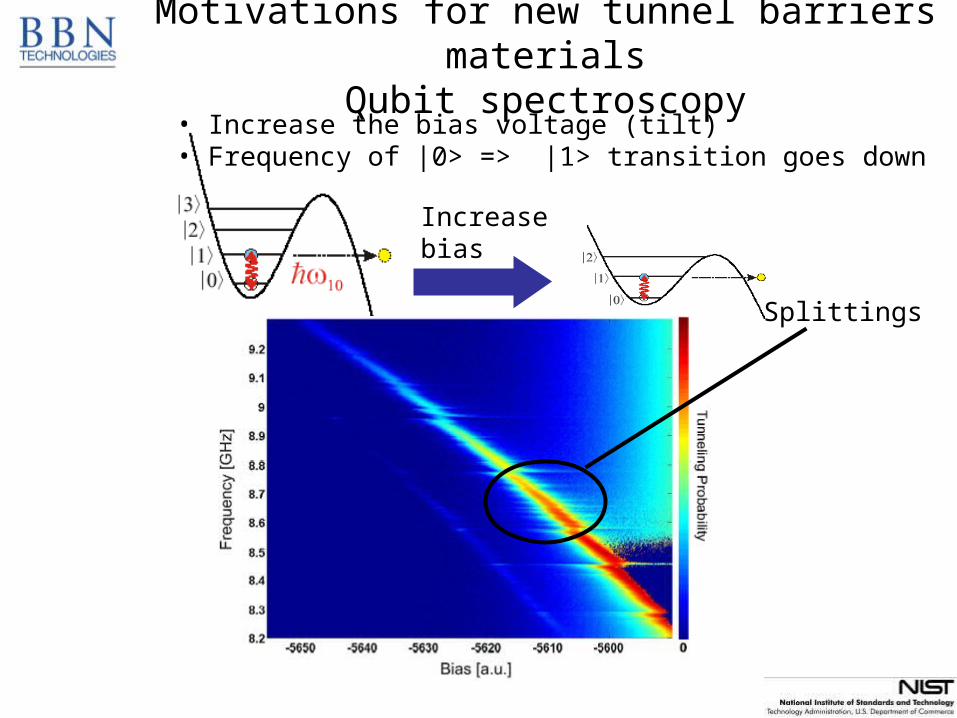
Motivations for new tunnel barriers materialsQubit spectroscopy
• Increase the bias voltage (tilt)• Frequency of |0> => |1> transition goes down
Splittings
Increasebias
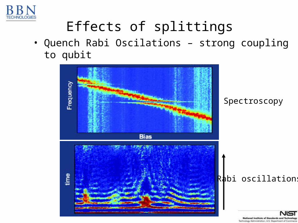
Effects of splittings• Quench Rabi Oscilations – strong coupling to qubit
Rabi oscillations
Spectroscopy
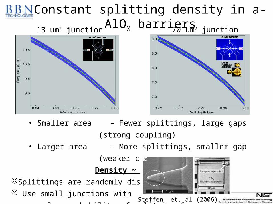
Constant splitting density in a-AlOX barriers13 um2 junction 70 um2 junction
• Smaller area – Fewer splittings, large gaps (strong coupling)
• Larger area - More splittings, smaller gap (weaker coupling)
Density ~ 1/GHz/m2
Splittings are randomly distributed
Use small junctions with
low probability of splitting for
test structures (< 1 m2)Steffen, et. al (2006)
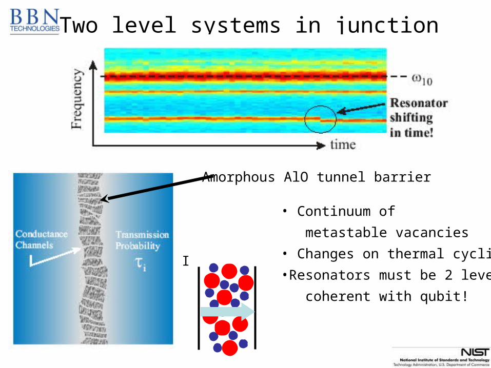
Two level systems in junction
Amorphous AlO tunnel barrier
• Continuum of
metastable vacancies
• Changes on thermal cycling
•Resonators must be 2 level,
coherent with qubit!
I
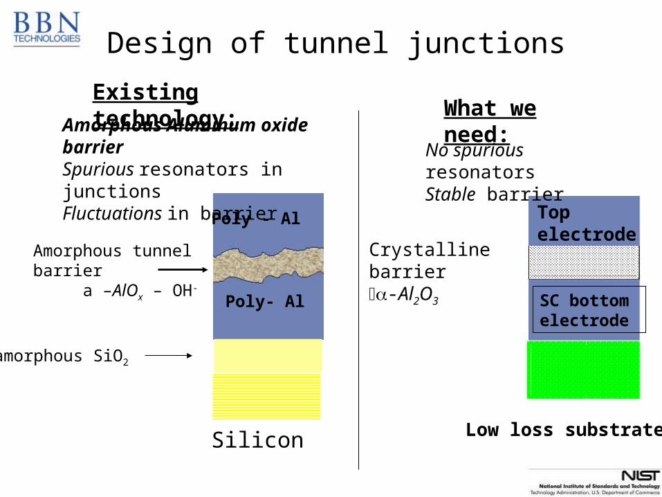
What we need:
Crystalline barrier-Al2O3
Poly - Al
Poly- Al
Existing technology:
Amorphous tunnel barrier a –AlOx – OH-
No spurious resonatorsStable barrier
Amorphous Aluminum oxide barrierSpurious resonators in junctionsFluctuations in barrier
Silicon
amorphous SiO2
Low loss substrate
Design of tunnel junctions
SC bottom electrode
Top electrode
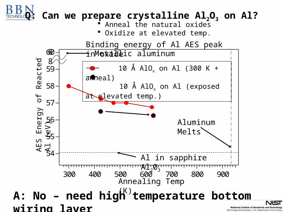
Q: Can we prepare crystalline Al2O3 on Al?
Binding energy of Al AES peak in oxide60
59
58
57
56
55
54
900800700600500400300Annealing Temp (K)
AE
S E
nerg
y of
Rea
cted
Al (
eV)
Al in sapphire Al203
Metallic aluminum
Aluminum Melts
68
10 Å AlOx on Al (300 K + anneal) 10 Å AlOx on Al (exposed at elevated temp.)
Anneal the natural oxides Oxidize at elevated temp.
A: No – need high temperature bottom wiring layer
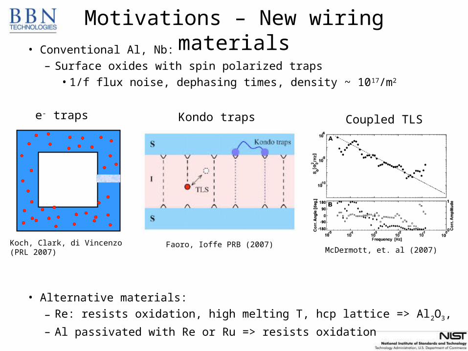
Motivations – New wiring materials• Conventional Al, Nb:
– Surface oxides with spin polarized traps• 1/f flux noise, dephasing times, density ~ 1017/m2
• Alternative materials:
– Re: resists oxidation, high melting T, hcp lattice => Al2O3,
– Al passivated with Re or Ru => resists oxidation
Koch, Clark, di Vincenzo(PRL 2007)
e- traps Kondo traps
Faoro, Ioffe PRB (2007)
Coupled TLS
McDermott, et. al (2007)
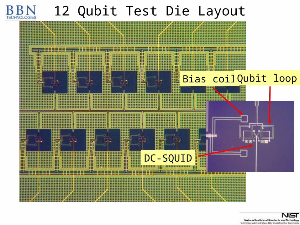
12 Qubit Test Die Layout
Bias coil Qubit loop
DC-SQUID
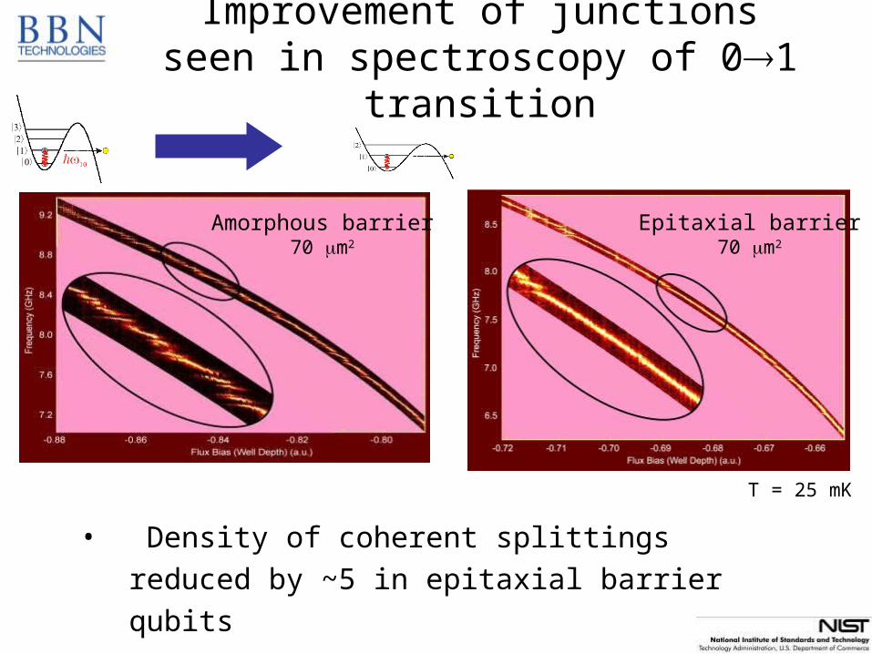
Improvement of junctionsseen in spectroscopy of 01 transition
T = 25 mK
Amorphous barrier70 m2
Epitaxial barrier70 m2
• Density of coherent splittings reduced by ~5
in epitaxial barrier qubits
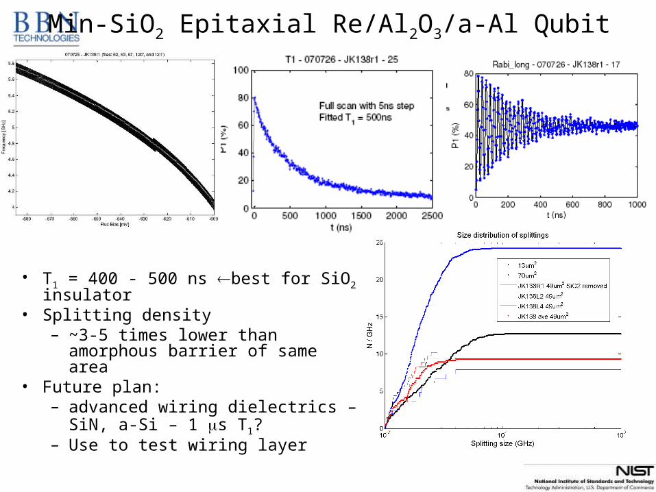
• T1 = 400 - 500 ns best for SiO2 insulator
• Splitting density– ~3-5 times lower than amorphous
barrier of same area• Future plan:
– advanced wiring dielectrics – SiN, a-Si – 1 s T1?
– Use to test wiring layer
Min-SiO2 Epitaxial Re/Al2O3/a-Al Qubit
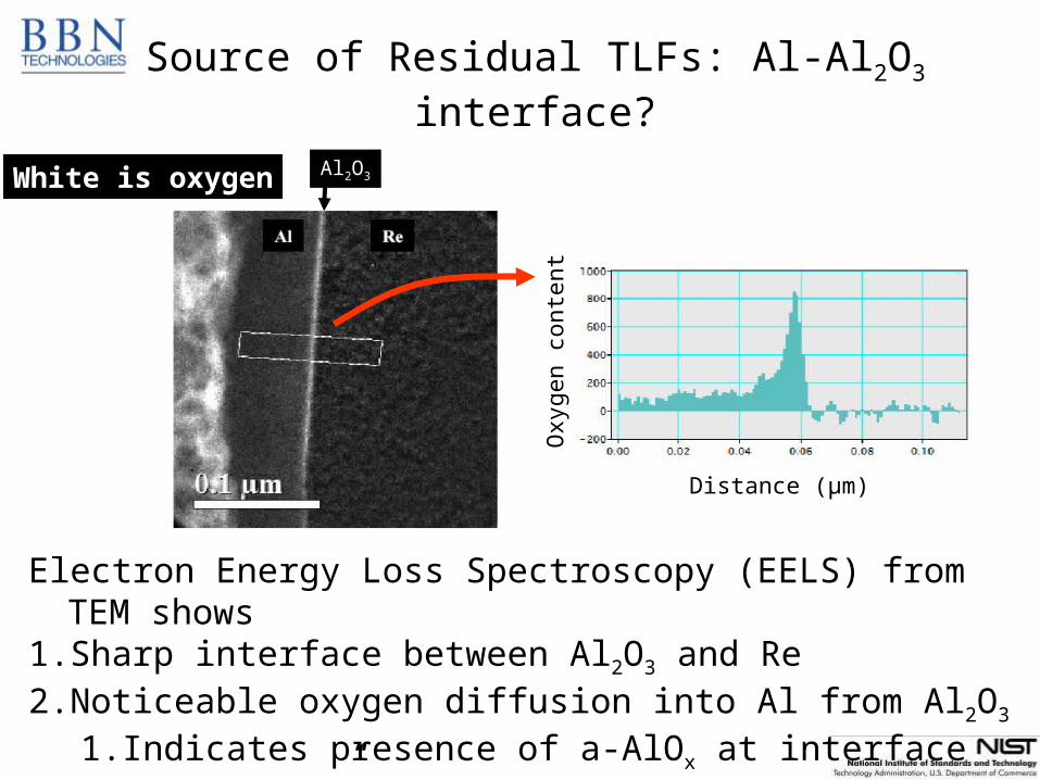
Source of Residual TLFs: Al-Al2O3 interface?
Electron Energy Loss Spectroscopy (EELS) from TEM shows1. Sharp interface between Al2O3 and Re2. Noticeable oxygen diffusion into Al from Al2O3
1. Indicates presence of a-AlOx at interface2. Will “heal” pinholes
Distance (μm)
Oxy
gen
cont
ent
Al2O3White is oxygen
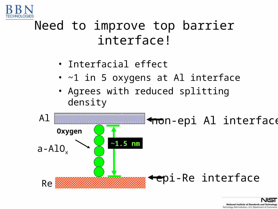
Need to improve top barrier interface!
• Interfacial effect• ~1 in 5 oxygens at Al interface• Agrees with reduced splitting density
~1.5 nm
epi-Re interface
non-epi Al interfaceOxygen
Re
Al
a-AlOx
0
5
10
15
20
25
0 100 200 300 400 500
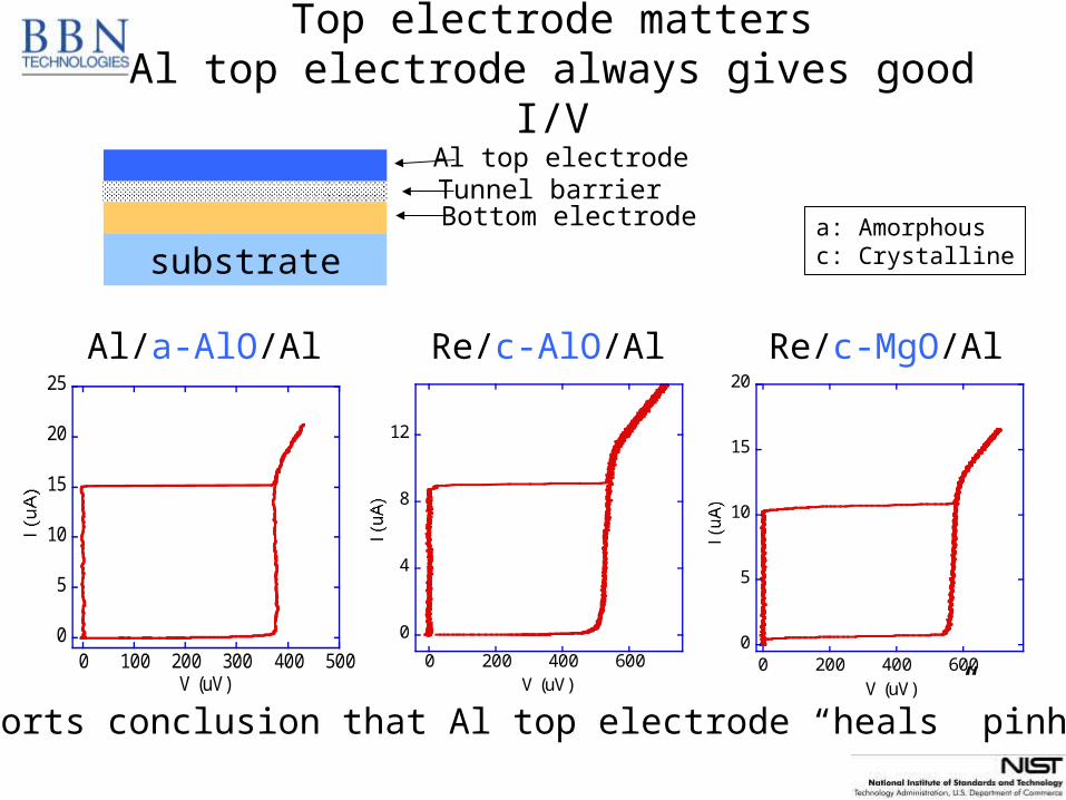
Al/a-AlOx/Al
V (uV)
Al/a-AlO/Al
0
4
8
12
0 200 400 600
Re/c-Al2O3/Al
V (uV)
Re/c-AlO/Al
0
5
10
15
20
0 200 400 600
Re/c-MgO/Al
V (uV)
Re/c-MgO/Al
a: Amorphousc: Crystalline
Supports conclusion that Al top electrode “heals” pinholes
substrate
Al top electrodeTunnel barrierBottom electrode
Top electrode mattersAl top electrode always gives good I/V
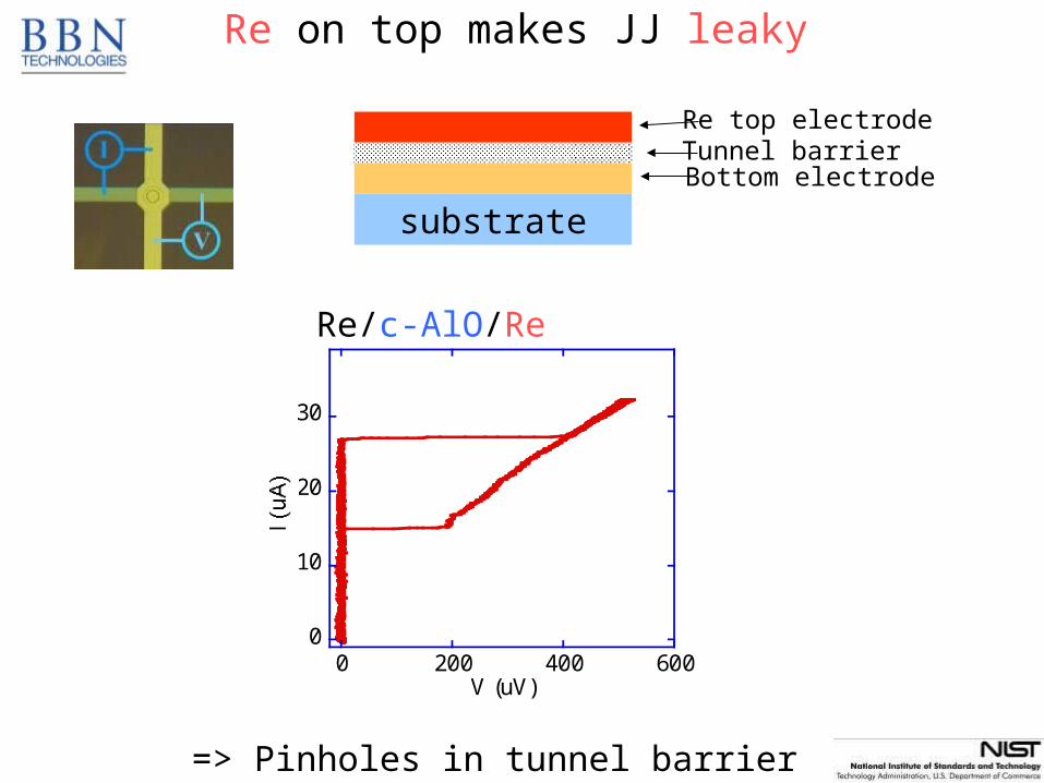
0
10
20
30
0 200 400 600
Re/c-Al2O3/Re/Al
V (uV)
Re/c-AlO/Re
substrate
Re top electrodeTunnel barrierBottom electrode
=> Pinholes in tunnel barrier
Re on top makes JJ leaky
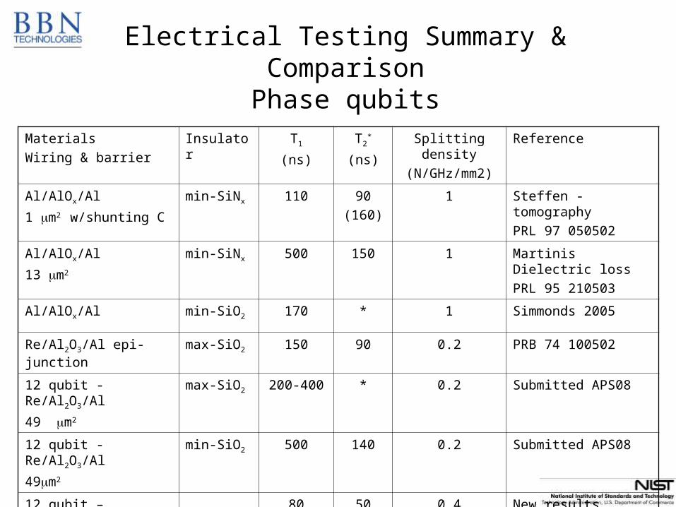
Electrical Testing Summary & ComparisonPhase qubits
Materials
Wiring & barrier
Insulator T1
(ns)
T2*
(ns)
Splitting density
(N/GHz/mm2)
Reference
Al/AlOx/Al
1 m2 w/shunting C
min-SiNx 110 90
(160)
1 Steffen - tomography
PRL 97 050502
Al/AlOx/Al
13 m2
min-SiNx 500 150 1 Martinis Dielectric loss
PRL 95 210503
Al/AlOx/Al min-SiO2 170 * 1 Simmonds 2005
Re/Al2O3/Al epi-junction max-SiO2 150 90 0.2 PRB 74 100502
12 qubit - Re/Al2O3/Al
49 m2
max-SiO2 200-400 * 0.2 Submitted APS08
12 qubit - Re/Al2O3/Al
49m2
min-SiO2 500 140 0.2 Submitted APS08
12 qubit – Re/MgO/Al 80 50 0.4 New results
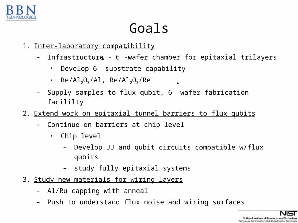
Goals1. Inter-laboratory compatibility
– Infrastructure - 6”-wafer chamber for epitaxial trilayers
• Develop 6” substrate capability
• Re/Al2O3/Al, Re/Al2O3/Re
– Supply samples to flux qubit, 6” wafer fabrication facililty
2. Extend work on epitaxial tunnel barriers to flux qubits
– Continue on barriers at chip level
• Chip level
– Develop JJ and qubit circuits compatible w/flux qubits
– study fully epitaxial systems
3. Study new materials for wiring layers
– Al/Ru capping with anneal
– Push to understand flux noise and wiring surfaces
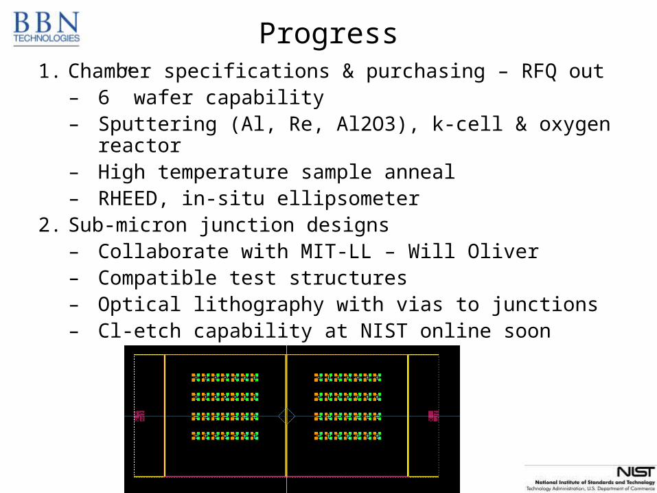
Progress1. Chamber specifications & purchasing – RFQ out
– 6” wafer capability– Sputtering (Al, Re, Al2O3), k-cell & oxygen reactor– High temperature sample anneal– RHEED, in-situ ellipsometer
2. Sub-micron junction designs– Collaborate with MIT-LL – Will Oliver– Compatible test structures– Optical lithography with vias to junctions– Cl-etch capability at NIST online soon
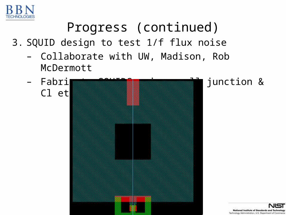
Progress (continued)3. SQUID design to test 1/f flux noise
– Collaborate with UW, Madison, Rob McDermott– Fabricate SQUIDS using small junction & Cl etch
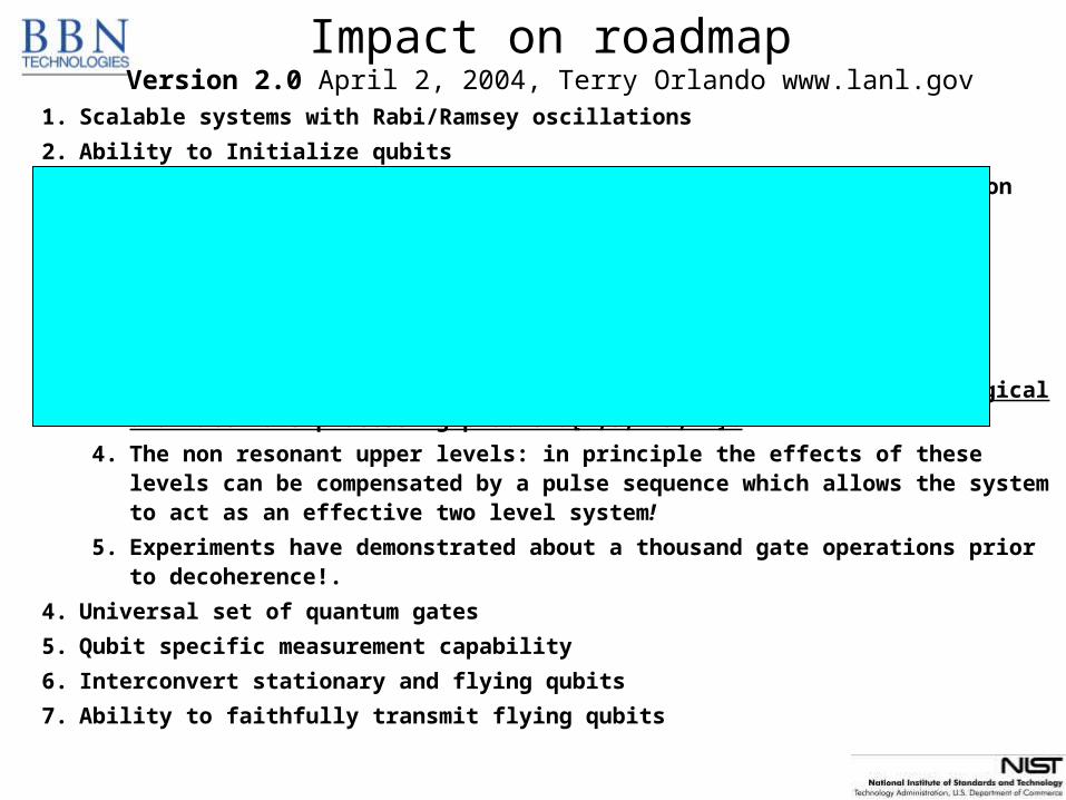
Impact on roadmapVersion 2.0 April 2, 2004, Terry Orlando www.lanl.gov
1. Scalable systems with Rabi/Ramsey oscillations
2. Ability to Initialize qubits
3. Long (relative) decoherence times, much longer than the gate-operation time
1. Calculations suggest the relaxation times ~ milliseconds.
2. Experimental measurements show at present a lower bounds
1. 1–10 μs for the Relaxation time
2. 0.1–0.5 μs for the dephasing time![2,3,7–9,11].
3. Charge, flux, and critical-current noise are probably a technological and materials processing problem![2,3,7–9,11].
4. The non resonant upper levels: in principle the effects of these levels can be compensated by a pulse sequence which allows the system to act as an effective two level system!
5. Experiments have demonstrated about a thousand gate operations prior to decoherence!.
4. Universal set of quantum gates
5. Qubit specific measurement capability
6. Interconvert stationary and flying qubits
7. Ability to faithfully transmit flying qubits
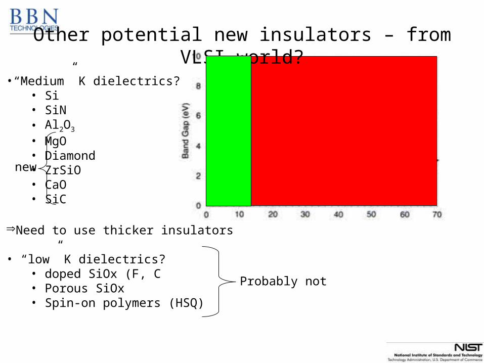
•“Medium” K dielectrics?• Si• SiN• Al2O3
• MgO• Diamond• ZrSiO• CaO• SiC
Need to use thicker insulators
• “low” K dielectrics? • doped SiOx (F, C• Porous SiOx• Spin-on polymers (HSQ)
Probably not
new
Other potential new insulators – from VLSI world?


![Panviva [Steve Pappas] CRM Roundtable](https://img.pdfslide.us/doc/110x75/58f01af91a28abaf7b8b4569/panviva-steve-pappas-crm-roundtable.jpg)