Embed Size (px)
Citation preview

1
Nick Sinev 2009 LCWS of the Americas, Vertex session October 1, 2009
Chronopixe first prototype testsChronopixe first prototype tests
J. E. Brau, N. B. Sinev, D. M. StromUniversity of Oregon, Eugene
C. Baltay, H. Neal, D. RabinowitzYale University, New Haven
EE work is contracted to Sarnoff Corporation

2
Nick Sinev 2009 LCWS of the Americas, Vertex session October 1, 2009
Outline of the talkOutline of the talk
Recall how chronopixel worksRecall how chronopixel works MilestonesMilestones Test stand designTest stand design Test Stand softwareTest Stand software Test plansTest plans Test resultsTest results Next stepsNext steps ConclusionsConclusions
3
Nick Sinev 2009 LCWS of the Americas, Vertex session October 1, 2009
How Chronopixel worksHow Chronopixel works
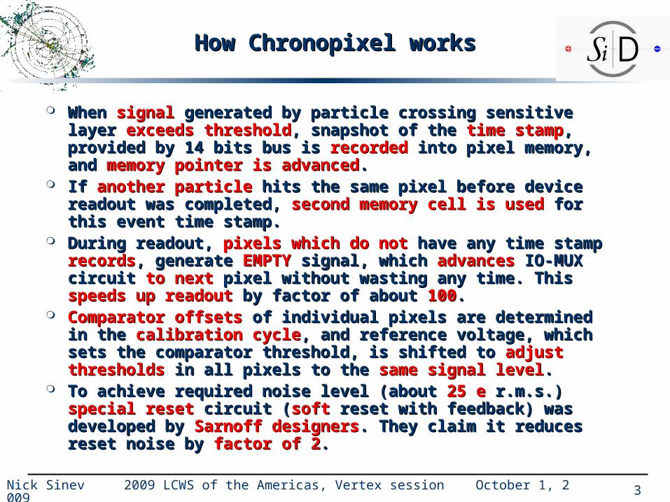
When When signal signal generated by particle crossing sensitive layer generated by particle crossing sensitive layer exceeds exceeds thresholdthreshold, snapshot of the , snapshot of the time stamptime stamp, provided by 14 bits bus is , provided by 14 bits bus is recordedrecorded into pixel memory, and into pixel memory, and memory pointer is advancedmemory pointer is advanced..
If If another particleanother particle hits the same pixel before device readout was hits the same pixel before device readout was completed, completed, second memory cell is usedsecond memory cell is used for this event time stamp. for this event time stamp.
During readout, During readout, pixels which do notpixels which do not have any time stamp have any time stamp recordsrecords, , generate generate EMPTYEMPTY signal, which signal, which advancesadvances IO-MUX circuit IO-MUX circuit to nextto next pixel without wasting any time. This pixel without wasting any time. This speeds up readoutspeeds up readout by factor of by factor of about about 100100..
Comparator offsetsComparator offsets of individual pixels are determined in the of individual pixels are determined in the calibration cyclecalibration cycle, and reference voltage, which sets the comparator , and reference voltage, which sets the comparator threshold, is shifted to threshold, is shifted to adjust thresholdsadjust thresholds in all pixels to the in all pixels to the same same signal levelsignal level..
To achieve required noise level (about To achieve required noise level (about 25 e25 e r.m.s.) r.m.s.) special resetspecial reset circuit (circuit (softsoft reset with feedback) was developed by reset with feedback) was developed by Sarnoff Sarnoff designersdesigners. They claim it reduces reset noise by . They claim it reduces reset noise by factor of 2factor of 2. .

4
Nick Sinev 2009 LCWS of the Americas, Vertex session October 1, 2009
Simplified Chronopixel SchematicSimplified Chronopixel Schematic
Essential features: Calibrator, special reset circuit
5
Nick Sinev 2009 LCWS of the Americas, Vertex session October 1, 2009
Calibration procedureCalibration procedure
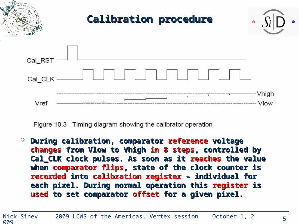
During calibration, comparator During calibration, comparator referencereference voltage voltage changeschanges from from Vlow to Vhigh Vlow to Vhigh in 8 stepsin 8 steps, controlled by Cal_CLK clock pulses. As , controlled by Cal_CLK clock pulses. As soon as it soon as it reachesreaches the value when the value when comparator flipscomparator flips, state of the , state of the clock counter is clock counter is recordedrecorded into into calibration registercalibration register – individual for – individual for each pixel. During normal operation this each pixel. During normal operation this registerregister is is used used to set to set comparator comparator offset offset for a given pixel.for a given pixel.

6
Nick Sinev 2009 LCWS of the Americas, Vertex session October 1, 2009
Sensor designSensor design
TSMC process TSMC process does notdoes not allow for creation of allow for creation of deep P-wellsdeep P-wells. Moreover, the . Moreover, the test chronopixel devices were test chronopixel devices were fabricatedfabricated using using low resistivitylow resistivity (~ 10 (~ 10 ohm*cm) epi layer. To be able to achieve comfortable depletion depth, ohm*cm) epi layer. To be able to achieve comfortable depletion depth, Pixel-B employs Pixel-B employs deep n-welldeep n-well, , encapsulatingencapsulating all all p-wellsp-wells in the NMOS gates. in the NMOS gates. This allow This allow application of negativeapplication of negative (up to -10 V) bias on (up to -10 V) bias on substratesubstrate..
Ultimate design, as envisioned Two sensor options in the fabricated chips
7
Nick Sinev 2009 LCWS of the Americas, Vertex session October 1, 2009
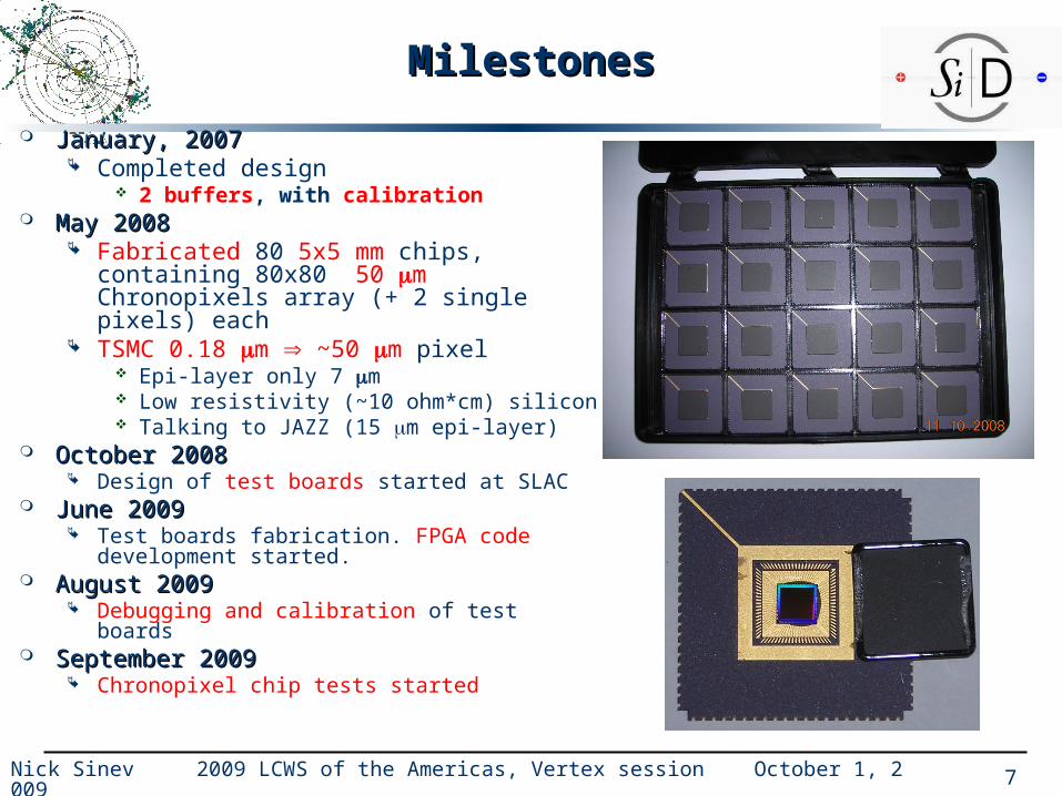
MilestonesMilestones
January, 2007January, 2007 Completed design
2 buffers, with calibration May 2008May 2008
Fabricated 80 5x5 mm chips, containing 80x80 50 m Chronopixels array (+ 2 single pixels) each
TSMC 0.18 m ~50 m pixel Epi-layer only 7 m Low resistivity (~10 ohm*cm) silicon Talking to JAZZ (15 m epi-layer)
October 2008October 2008 Design of test boards started at SLAC
June 2009June 2009 Test boards fabrication. FPGA code development
started. August 2009August 2009
Debugging and calibration of test boards September 2009September 2009
Chronopixel chip tests started

8
Nick Sinev 2009 LCWS of the Americas, Vertex session October 1, 2009
Test stand design. Block-diagram of FPGA Test stand design. Block-diagram of FPGA boardboard

9
Nick Sinev 2009 LCWS of the Americas, Vertex session October 1, 2009
Block-diagram of chronopixel test boardBlock-diagram of chronopixel test board

10
Nick Sinev 2009 LCWS of the Americas, Vertex session October 1, 2009
Test stand softwareTest stand software
Since May 2008 I started development of Since May 2008 I started development of test stand softwaretest stand software.. Graphical User InterfaceGraphical User Interface was developed on the basis of was developed on the basis of Motiff Motiff
library for Unix.library for Unix. Main Main ideaidea of how to provide large number of of how to provide large number of different control different control
signal waveformssignal waveforms was to use very fast was to use very fast waveform memorywaveform memory in the in the Xilinx FPGA. Memory has 32 bit wide words, and its capacity is Xilinx FPGA. Memory has 32 bit wide words, and its capacity is 4096 such words. 4096 such words. Each bit of the memoryEach bit of the memory output register is output register is connected to some of connected to some of chronopix control signalchronopix control signal wire. Memory wire. Memory addressaddress is increasing with is increasing with 80 MHz rate80 MHz rate. So control signals have time . So control signals have time bin width of bin width of 12.5 ns12.5 ns..
There is another, There is another, larger memorylarger memory (24 bits wide 16 kwords) for (24 bits wide 16 kwords) for storing storing read back dataread back data from chrono from chrono pixelspixels..
EverythingEverything in test stand software is in test stand software is configuredconfigured by set of by set of text filestext files in in configuration directory. These text files contain all configuration directory. These text files contain all voltage settingsvoltage settings, , all all waveforms informationwaveforms information and and listlist of all of all monitored voltagesmonitored voltages and and currents currents together with together with calibrationcalibration constants. constants.

11
Nick Sinev 2009 LCWS of the Americas, Vertex session October 1, 2009
Test stand software - continueTest stand software - continue
Configuration directory also contains Configuration directory also contains list of commandslist of commands, which are , which are assigned to buttonsassigned to buttons on the GUI. This list on the GUI. This list can be changedcan be changed, and , and command buttons numbercommand buttons number and assigned and assigned commandscommands will will changechange withoutwithout need of any code need of any code recompilingrecompiling..
All commands (performed by button clicks), are All commands (performed by button clicks), are automatically automatically savedsaved in log files. Log files are named by current date, and each day in log files. Log files are named by current date, and each day will have only one log file, even if you restart GUI many times. Log will have only one log file, even if you restart GUI many times. Log file contains also all file contains also all voltage settingsvoltage settings..
Another Another file, automatically createdfile, automatically created and filled is the and filled is the monitored monitored valuesvalues records. records.
Yet another Yet another files, created automaticallyfiles, created automatically by some of the tests – by some of the tests – KUMACKUMAC files for use with PAW files for use with PAW
For every KUMAC file, record in the For every KUMAC file, record in the testcond.txt testcond.txt file is created, file is created, containing containing specific settingsspecific settings for the test and for the test and operator commentsoperator comments..

12
Nick Sinev 2009 LCWS of the Americas, Vertex session October 1, 2009
Test Stand GUITest Stand GUI

13
Nick Sinev 2009 LCWS of the Americas, Vertex session October 1, 2009
Waveform Display ExampleWaveform Display Example
Test Stand GUI has a button for displaying waveforms. You can select (from drop down menus) which waveforms to display, the mode of operation to display, and clocks range – as some waveform may be too long to be shown on the display from start to the end.Example at right – waveforms used in most noise measurements with Test Pixel A. They provide initial reset memory to 0, then manipulations to record comparator status, and then reading out results. As soon as file, describing WF is modified, new waveforms immediately can be displayed, no need to restart GUI.New waveform display always create new window, so you can easily compare different waveforms by keeping old windows open.

14
Nick Sinev 2009 LCWS of the Americas, Vertex session October 1, 2009
Example of waveform describing fileExample of waveform describing file
15
Nick Sinev 2009 LCWS of the Americas, Vertex session October 1, 2009
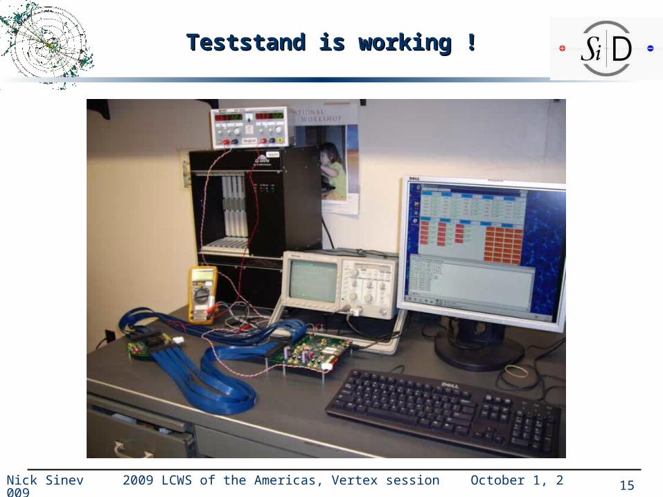
Teststand is working !Teststand is working !
16
Nick Sinev 2009 LCWS of the Americas, Vertex session October 1, 2009
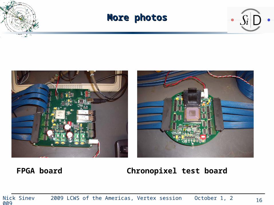
More photosMore photos
FPGA board Chronopixel test board
17
Nick Sinev 2009 LCWS of the Americas, Vertex session October 1, 2009
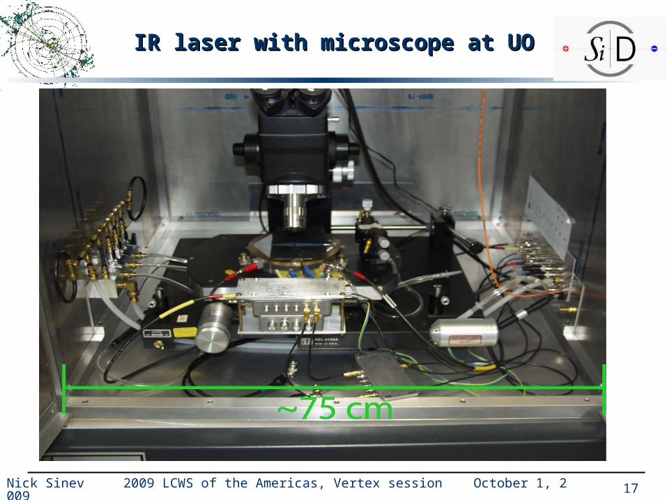
IR laser with microscope at UOIR laser with microscope at UO

18
Nick Sinev 2009 LCWS of the Americas, Vertex session October 1, 2009
Tests planTests plan
First tests will be done with single pixels (Test pixel A and B) to learn how First tests will be done with single pixels (Test pixel A and B) to learn how everything works.everything works.
The most important part of the tests is to check, if The most important part of the tests is to check, if calibrationcalibration procedure procedure worksworks, and is , and is 2 mV2 mV range range enoughenough to cover offsets in all pixels. to cover offsets in all pixels.
Next test will be to check Next test will be to check memorymemory operations. In principle, writing into operations. In principle, writing into time stamps memory is only done by pixel comparator, sensing signal. But time stamps memory is only done by pixel comparator, sensing signal. But for testingfor testing of memory proper operation, external of memory proper operation, external writewrite signal can be used to signal can be used to record any valuerecord any value into all memory cells simultaneously and when into all memory cells simultaneously and when read it read it backback cell by cell. cell by cell.
If If everything goes smootheverything goes smooth, even for some part of the pixels, , even for some part of the pixels, Fe55 Fe55 source can source can be used to determine be used to determine sensitivitysensitivity (expected 10 (expected 10 μμV/e) and V/e) and noise levelnoise level (by the (by the width of Fe55 peak).width of Fe55 peak).
After that After that tests with IR lasertests with IR laser will follow to check time stamping operations. will follow to check time stamping operations. Of course, Of course, power consumptionpower consumption, and all questions concerning 3MHz time , and all questions concerning 3MHz time
stamp bus (crosstalk, recording errors) operation should be investigated.stamp bus (crosstalk, recording errors) operation should be investigated.

19
Nick Sinev 2009 LCWS of the Americas, Vertex session October 1, 2009
First results-noise measurementsFirst results-noise measurements
Horizontal axis on the plot at left Horizontal axis on the plot at left shows shows comparator thresholdcomparator threshold (set (set by connecting reference input of by connecting reference input of comparator to calibration selected comparator to calibration selected tap of resistive ladder and setting tap of resistive ladder and setting voltages voltages Vlow and VhighVlow and Vhigh, on the , on the ends of the ladder. (These voltages ends of the ladder. (These voltages differ only by 2 mVdiffer only by 2 mV !). Values !). Values shown on x axis are Vhigh. Vlow shown on x axis are Vhigh. Vlow is always by 2 mV lower.is always by 2 mV lower.
Vertical axis shows number of Vertical axis shows number of cases than comparator cases than comparator at the at the samplingsampling moment appeared moment appeared firedfired (which means it sensed input (which means it sensed input voltage as lower than reference – voltage as lower than reference – remember we expect negative remember we expect negative signals). Notice, entire range of x signals). Notice, entire range of x axis values is only 2 mV on this axis values is only 2 mV on this plot!plot!
20
Nick Sinev 2009 LCWS of the Americas, Vertex session October 1, 2009
Test results - continueTest results - continue
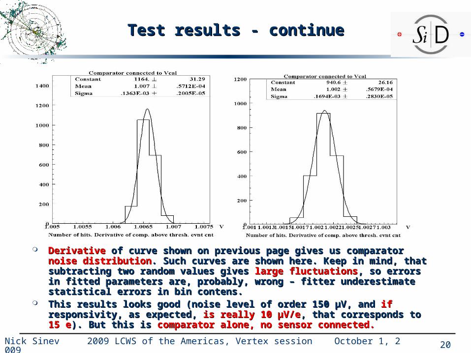
DerivativeDerivative of curve shown on previous page gives us comparator of curve shown on previous page gives us comparator noise distributionnoise distribution. . Such curves are shown here. Keep in mind, that subtracting two random values gives Such curves are shown here. Keep in mind, that subtracting two random values gives large fluctuationslarge fluctuations, so errors in fitted parameters are, probably, wrong – fitter , so errors in fitted parameters are, probably, wrong – fitter underestimate statistical errors in bin contens.underestimate statistical errors in bin contens.
This results looks good (noise level of order 150 This results looks good (noise level of order 150 μμV, and V, and ifif responsivity, as expected, responsivity, as expected, is really 10 is really 10 μμV/eV/e, that corresponds to , that corresponds to 15 e15 e). But this is ). But this is comparator alone, no sensor comparator alone, no sensor connected.connected.
21
Nick Sinev 2009 LCWS of the Americas, Vertex session October 1, 2009
Noise with sensor connectedNoise with sensor connected
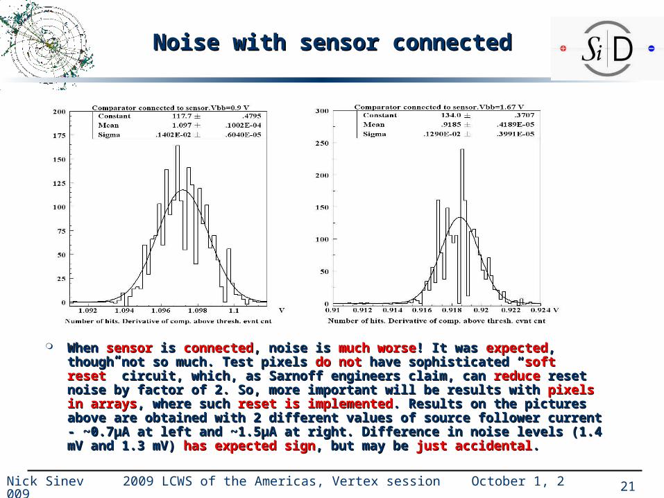
When When sensorsensor is is connectedconnected, noise is , noise is much worsemuch worse! It was ! It was expectedexpected, though not so much. , though not so much. Test pixels Test pixels do notdo not have sophisticated “ have sophisticated “soft resetsoft reset” circuit, which, as Sarnoff engineers ” circuit, which, as Sarnoff engineers claim, can claim, can reducereduce reset noise by factor of 2. So, more important will be results with reset noise by factor of 2. So, more important will be results with pixels in arrayspixels in arrays, where such , where such reset is implementedreset is implemented. Results on the pictures above are . Results on the pictures above are obtained with 2 different values of source follower current - ~0.7obtained with 2 different values of source follower current - ~0.7μμA at left and A at left and ~1.5~1.5μμA at right. Difference in noise levels (1.4 mV and 1.3 mV) A at right. Difference in noise levels (1.4 mV and 1.3 mV) has expected signhas expected sign, but , but may be may be just accidentaljust accidental..

22
Nick Sinev 2009 LCWS of the Americas, Vertex session October 1, 2009
Table of noise measurementsTable of noise measurements
You can see for yourself how thing are stable, if there temperature You can see for yourself how thing are stable, if there temperature dependence and how worse noise with sensor connected is (dependence and how worse noise with sensor connected is (in redin red).).
DateDate Chip #Chip # Comp inComp in TempTemp VbbVbb Peak posPeak pos SigmaSigma
Sept 23Sept 23 44 Vc=1.000 VVc=1.000 V ~35 C~35 C 1.25 V1.25 V 1.0066 V1.0066 V 136 136 μμVV
Sept 23Sept 23 44 SensorSensor ~35 C~35 C 1.25 V1.25 V 1.0198 V1.0198 V 1.44 mV1.44 mV
Sept 24Sept 24 55 Vc=1.000 VVc=1.000 V ~35 C~35 C 1.25 V1.25 V 1.0032 V1.0032 V 266 266 μμVV
Sept 24Sept 24 55 Vc=1.000 VVc=1.000 V ~35 C~35 C 1.25 V1.25 V 1.0032 V1.0032 V 271 271 μμVV
Sept 24Sept 24 55 Vc=1.000 VVc=1.000 V ~28 C~28 C 1.25 V1.25 V 1.0021 V1.0021 V 170 170 μμVV
Sept 25Sept 25 55 Vc=1.000 VVc=1.000 V ~35 C~35 C 1.25 V1.25 V 1.0032 V1.0032 V 229 229 μμVV
Sept 25Sept 25 55 Vc=0.999 VVc=0.999 V ~35 C~35 C 1.25 V1.25 V 1.0022 V1.0022 V 224 224 μμVV
Sept 25Sept 25 55 Vc=1.000 VVc=1.000 V ~28 C~28 C 1.25 V1.25 V 1.0016 V1.0016 V 170 170 μμVV
Sept 26Sept 26 55 Vc=1.000 VVc=1.000 V ~35 C~35 C 1.25 V1.25 V 1.0017 V1.0017 V 183 183 μμVV
Sept 26Sept 26 55 SensorSensor ~35 C~35 C 1.67 V1.67 V 0.9185 V0.9185 V 1.29 mV1.29 mV
Sept 26Sept 26 55 SensorSensor ~35 C~35 C 0.9 V0.9 V 1.0970 V1.0970 V 1.40 mV1.40 mV

23
Nick Sinev 2009 LCWS of the Americas, Vertex session October 1, 2009
First glance at pixel arraysFirst glance at pixel arrays
Here you can see Here you can see comparisoncomparison of code of code writtenwritten in individual pixels memory with in individual pixels memory with read read backback values. Picture at left is for recorded code = values. Picture at left is for recorded code = 0x3fff0x3fff, at right for code = , at right for code = 00. . Green Green read back is the read back is the samesame as written, as written, redred – – differentdifferent, , blueblue – corresponds to – corresponds to code written code written into another cellinto another cell (recall each pixel has 2 memory cells). Pixel array A is in left 40 (recall each pixel has 2 memory cells). Pixel array A is in left 40 columns, B – right columns. columns, B – right columns.

24
Nick Sinev 2009 LCWS of the Americas, Vertex session October 1, 2009
First glance at arrays - continueFirst glance at arrays - continue
Pictures on Pictures on previous slideprevious slide do do notnot tell tell all storyall story. Here you can see . Here you can see column decodercolumn decoder readings. Upper readings. Upper 40 rows behave exactly 40 rows behave exactly as as expectedexpected – every next pixel has – every next pixel has column number increased by 1, column number increased by 1, but in but in lower 40 rowslower 40 rows readings are readings are chaoticchaotic. I think something is . I think something is wrong with wrong with row number decodingrow number decoding – either in the chip, or in our test – either in the chip, or in our test board connection to correct pins board connection to correct pins encoding row number. encoding row number.
Remember, it is Remember, it is first tryfirst try – I did – I did not have time to debug things. I not have time to debug things. I am showing it, to demonstrate, am showing it, to demonstrate, that that in general pixel array logic is in general pixel array logic is workingworking. And to brag about my . And to brag about my pixels display.pixels display.
25
Nick Sinev 2009 LCWS of the Americas, Vertex session October 1, 2009
Next StepsNext Steps
September – December 2009 September – December 2009 Test and characterize prototype 1 Design prototype 2 (with Sarnoff) and start fabrication
January 2010 – September 2010January 2010 – September 2010 Finish fabrication of prototype 2 Design and implement modification of test boards Test prototype 2 Design prototype 3 with Sarnoff and start fabrication
October 2010 – September 2011October 2010 – September 2011 Test prototype 3 – close to real detector for ILC

26
Nick Sinev 2009 LCWS of the Americas, Vertex session October 1, 2009
ConclusionsConclusions
First chronopixel prototypes have been First chronopixel prototypes have been fabricated, packaged fabricated, packaged delivereddelivered to SLAC and are been tested. to SLAC and are been tested.
Tests show that general Tests show that general concept is workingconcept is working, but we need to do much , but we need to do much more measurements before we can characterize its performance.more measurements before we can characterize its performance.
It is obvious now, that at least It is obvious now, that at least some correctionssome corrections to design will be to design will be neededneeded..
We are looking for the manufacturer of the next prototype We are looking for the manufacturer of the next prototype implementing implementing deep P-welldeep P-well. Depending on how much correction to . Depending on how much correction to the design will be needed, the design will be needed, next prototypenext prototype may be ready for may be ready for submission at the submission at the end 2009end 2009 – beginning 2010. It still will be 50x50 – beginning 2010. It still will be 50x50 μμm pixels, but completely operational, m pixels, but completely operational, 100% efficient100% efficient device. device.
After that accomplished, After that accomplished, scaling to 45 nmscaling to 45 nm technology may be technology may be thought. So, funding depending, we can be ready to start design of thought. So, funding depending, we can be ready to start design of final vertex detector sensors in final vertex detector sensors in 2010-20112010-2011..