Embed Size (px)
Citation preview
8051 MicrocontrollerMemory Organization
Prof. Anish Goel
Embedded Systems
Memory Organization
Embedded Systems Prof. Anish Goel2
The 8051 has two types of memory and these areProgram Memory and Data Memory.
Program Memory (ROM) is used to permanently save theprogram being executed, while Data Memory (RAM) isused for temporarily storing data and intermediate resultscreated and used during the operation of themicrocontroller.
Depending on the model in use at most a few Kb of ROMand 128 or 256 bytes of RAM is used.
All 8051 microcontrollers have a 16-bit addressing busand are capable of addressing 64 kb memory.
Program Memory
Embedded Systems Prof. Anish Goel3
The first models of the 8051 microcontroller family did not haveinternal program memory.
It was added as an external separate chip. These models are recognizable by their label beginning with 803 (for
example 8031 or 8032). All later models have a few Kbyte ROM embedded. Even though such an amount of memory is sufficient for writing
most of the programs, there are situations when it is necessary touse additional memory as well.
A typical example are so called lookup tables. They are used in cases when equations describing some processes
are too complicated or when there is no time for solving them. In such cases all necessary estimates and approximates are executed
in advance and the final results are put in the tables (similar tologarithmic tables).
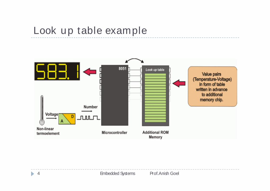
Look up table example
Embedded Systems Prof. Anish Goel4
External Memory Access
Embedded Systems Prof. Anish Goel5
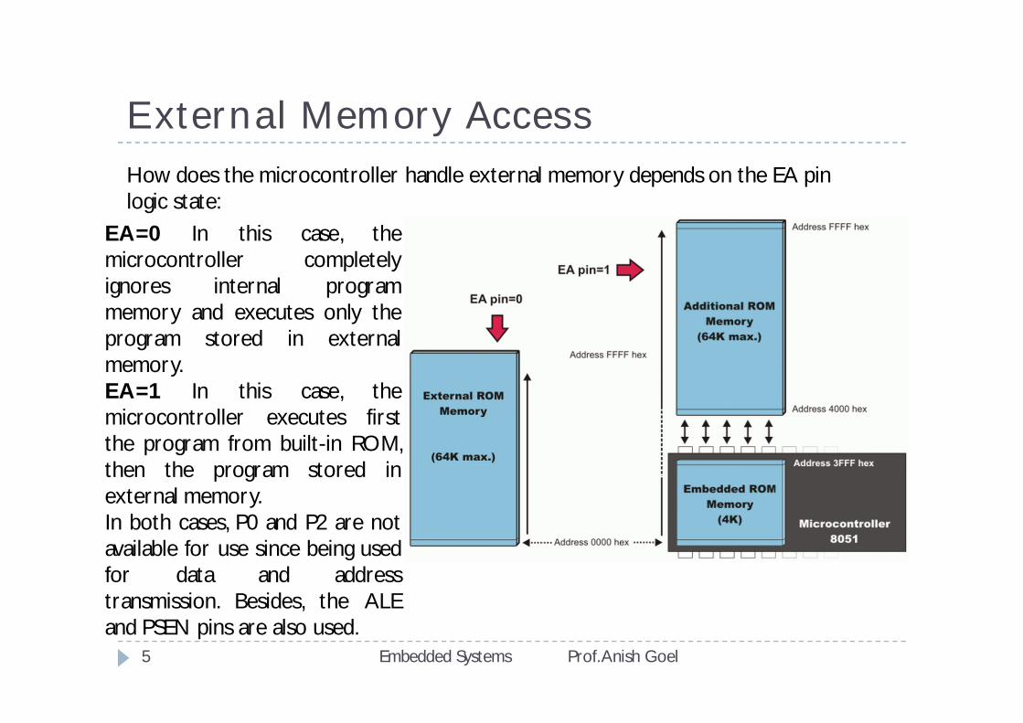
How does the microcontroller handle external memory depends on the EA pin logic state:
EA=0 In this case, themicrocontroller completelyignores internal programmemory and executes only theprogram stored in externalmemory.EA=1 In this case, themicrocontroller executes firstthe program from built-in ROM,then the program stored inexternal memory.In both cases, P0 and P2 are notavailable for use since being usedfor data and addresstransmission. Besides, the ALEand PSEN pins are also used.
Data Memory
Embedded Systems Prof. Anish Goel6
Data Memory is used for temporarily storing data andintermediate results created and used during the operation ofthe microcontroller.
Besides, RAM memory built in the 8051 family includes manyregisters such as hardware counters and timers, input/outputports, serial data buffers etc.
The previous models had 256 RAM locations, while for thelater models this number was incremented by additional 128registers.
However, the first 256 memory locations (addresses 0-FFh)are the heart of memory common to all the models belongingto the 8051 family.
Locations available to the user occupy memory space withaddresses 0-7Fh, i.e. first 128 registers. This part of RAM isdivided in several blocks.
Data Memory
Embedded Systems Prof. Anish Goel7
The first block consists of 4 banks each including 8 registersdenoted by R0-R7.
Prior to accessing any of these registers, it is necessary toselect the bank containing it.
The next memory block (address 20h-2Fh) is bit- addressable,which means that each bit has its own address (0-7Fh).
Since there are 16 such registers, this block contains in total of128 bits with separate addresses (address of bit 0 of the 20hbyte is 0, while address of bit 7 of the 2Fh byte is 7Fh).
The third group of registers occupy addresses 2Fh-7Fh, i.e. 80locations, and does not have any special functions or features.
Memory expansion
Embedded Systems Prof. Anish Goel8
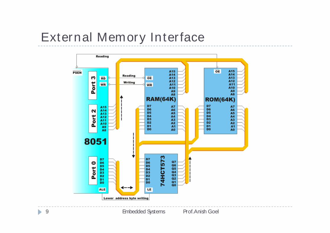
In case memory (RAM or ROM) built in themicrocontroller is not sufficient, it is possible to add twoexternal memory chips with capacity of 64Kb each. P2and P3 I/O ports are used for their addressing and datatransmission.
External Memory Interface
Embedded Systems Prof. Anish Goel9
External Memory Interface
Embedded Systems Prof. Anish Goel10
From the user’s point of view, everything works quitesimply when properly connected because mostoperations are performed by the microcontroller itself.
The 8051 microcontroller has two pins for data readRD#(P3.7) and PSEN#.
The first one is used for reading data from external datamemory (RAM), while the other is used for reading datafrom external program memory (ROM).
Both pins are active low. A typical example of memoryexpansion by adding RAM and ROM chips is shown infigure above.
External Memory Interface
Embedded Systems Prof. Anish Goel11
When the program during execution encounters an instructionwhich resides in external memory (ROM), the microcontroller willactivate its control output ALE and set the first 8 bits of address(A0-A7) on P0. IC circuit 74HCT573 passes the first 8 bits tomemory address pins.
A signal on the ALE pin latches the IC circuit 74HCT573 andimmediately afterwards 8 higher bits of address (A8-A15) appear onthe port. In this way, a desired location of additional programmemory is addressed. It is left over to read its content.
Port P0 pins are configured as inputs, the PSEN pin is activated andthe microcontroller reads from memory chip.
Similar occurs when it is necessary to read location from externalRAM. Addressing is performed in the same way, while read and writeare performed via signals appearing on the control outputs RD (isshort for read) or WR (is short for write).
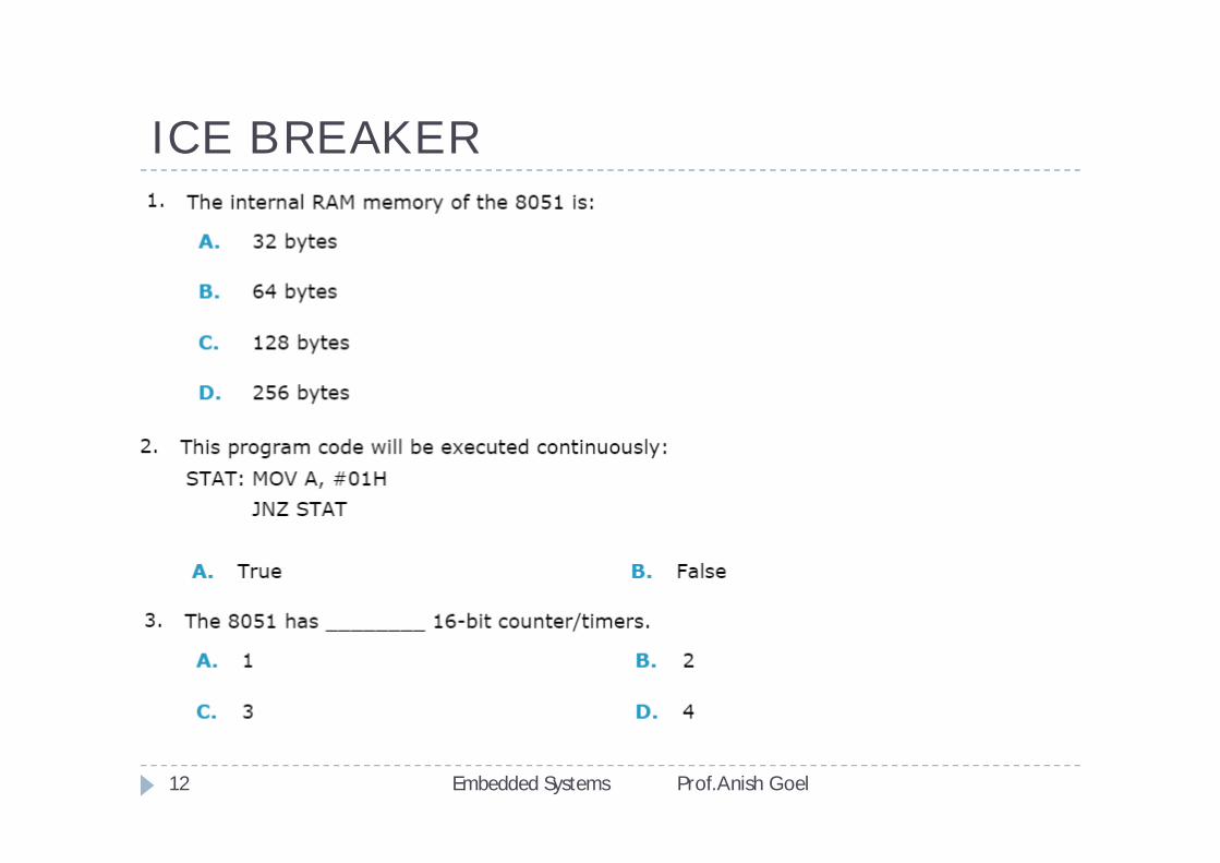
ICE BREAKER
Embedded Systems Prof. Anish Goel12
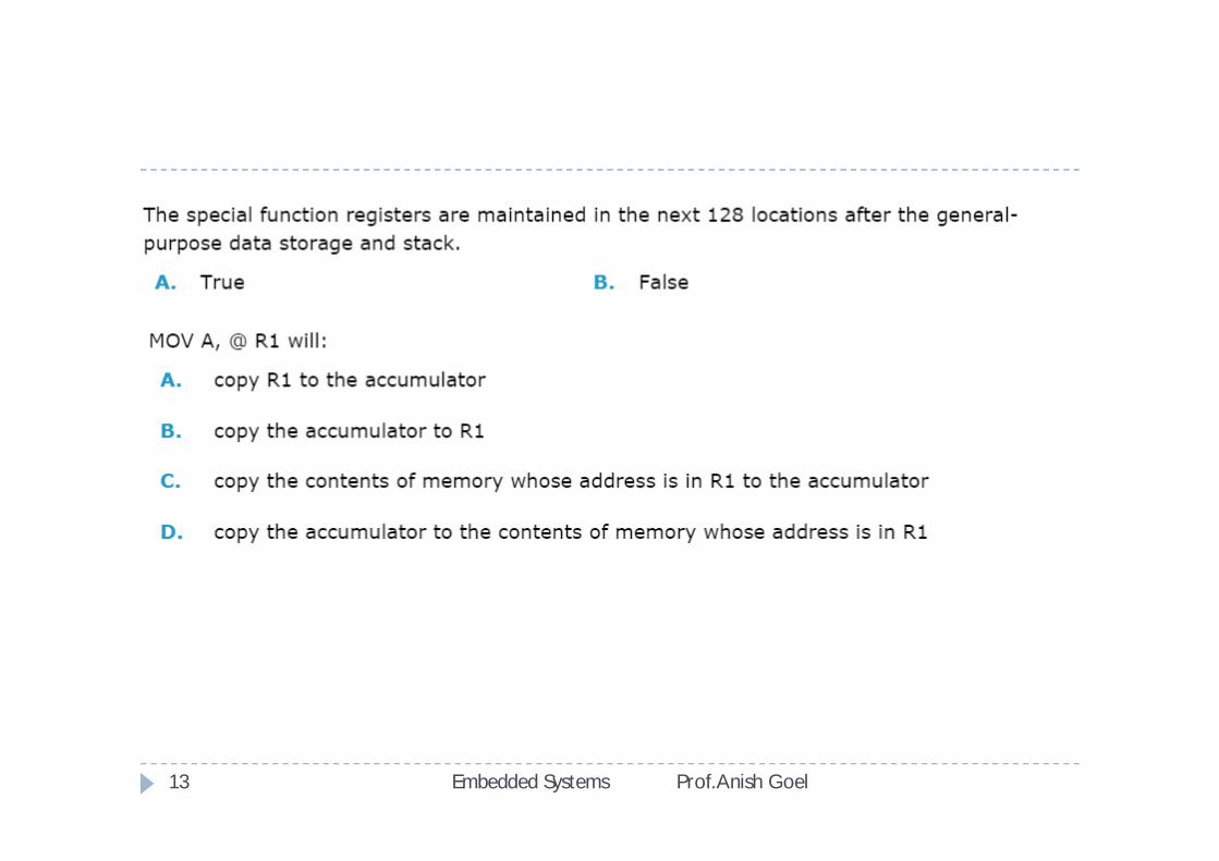
Embedded Systems Prof. Anish Goel13
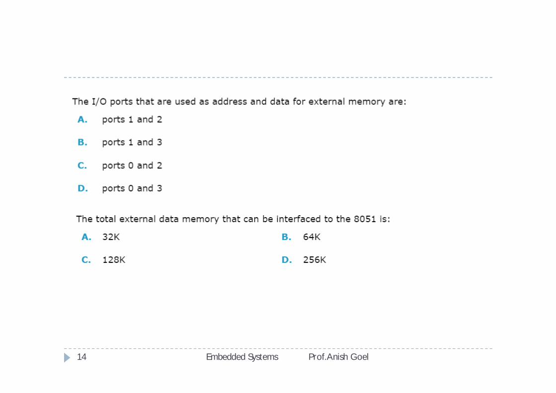
Embedded Systems Prof. Anish Goel14
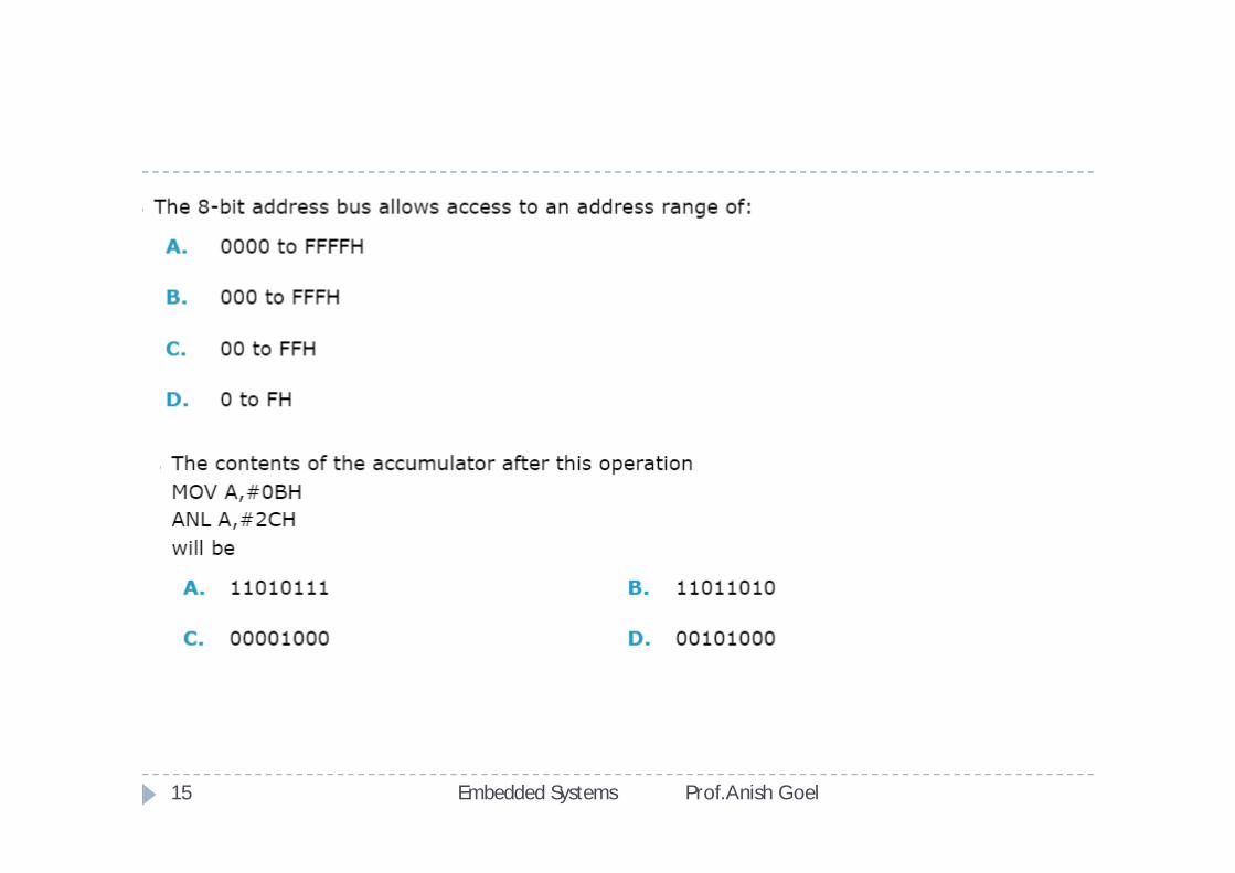
Embedded Systems Prof. Anish Goel15


![02-PPT Matematika III [TM1]](https://img.pdfslide.us/doc/110x75/577c7c1b1a28abe054994f77/02-ppt-matematika-iii-tm1.jpg)