Embed Size (px)
Citation preview
CHAPTER 4 : ELECTRONICS
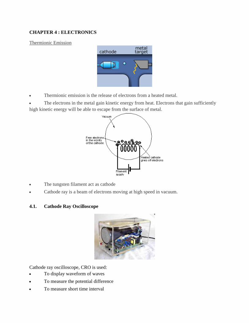
Thermionic Emission
Thermionic emission is the release of electrons from a heated metal.
The electrons in the metal gain kinetic energy from heat. Electrons that gain sufficiently
high kinetic energy will be able to escape from the surface of metal.
The tungsten filament act as cathode
Cathode ray is a beam of electrons moving at high speed in vacuum.
4.1. Cathode Ray Oscilloscope
Cathode ray oscilloscope, CRO is used:
To display waveform of waves
To measure the potential difference
To measure short time interval
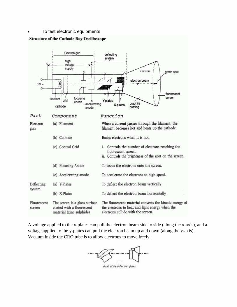
To test electronic equipments
A voltage applied to the x-plates can pull the electron beam side to side (along the x-axis), and a
voltage applied to the y-plates can pull the electron beam up and down (along the y-axis).
Vacuum inside the CRO tube is to allow electrons to move freely.
Properties of cathode ray:
Moves in straight line
Carries momentum and energy
Are charged negative
Can be deflected by electric field
Can be deflected by magnetic field.
Can produce fluorescence when they strike at fluorescent material
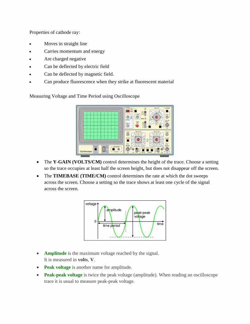
Measuring Voltage and Time Period using Oscilloscope
The Y-GAIN (VOLTS/CM) control determines the height of the trace. Choose a setting
so the trace occupies at least half the screen height, but does not disappear off the screen.
The TIMEBASE (TIME/CM) control determines the rate at which the dot sweeps
across the screen. Choose a setting so the trace shows at least one cycle of the signal
across the screen.
Amplitude is the maximum voltage reached by the signal.
It is measured in volts, V.
Peak voltage is another name for amplitude.
Peak-peak voltage is twice the peak voltage (amplitude). When reading an oscilloscope
trace it is usual to measure peak-peak voltage.
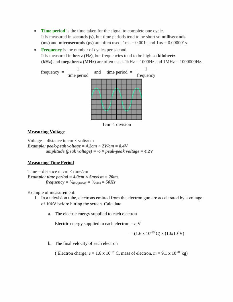
Time period is the time taken for the signal to complete one cycle.
It is measured in seconds (s), but time periods tend to be short so milliseconds
(ms) and microseconds (µs) are often used. 1ms = 0.001s and 1µs = 0.000001s.
Frequency is the number of cycles per second.
It is measured in hertz (Hz), but frequencies tend to be high so kilohertz
(kHz) and megahertz (MHz) are often used. 1kHz = 1000Hz and 1MHz = 1000000Hz.
frequency = 1
and time period = 1
time period frequency
1cm=1 division
Measuring Voltage
Voltage = distance in cm × volts/cm
Example: peak-peak voltage = 4.2cm × 2V/cm = 8.4V
amplitude (peak voltage) = ½ × peak-peak voltage = 4.2V
Measuring Time Period
Time = distance in cm × time/cm
Example: time period = 4.0cm × 5ms/cm = 20ms
frequency = 1/time period = 1/20ms = 50Hz
Example of measurement:
1. In a television tube, electrons emitted from the electron gun are accelerated by a voltage
of 10kV before hitting the screen. Calculate
a. The electric energy supplied to each electron
Electric energy supplied to each electron = e.V
= (1.6 x 10⁻¹⁹ C) x (10x103V)
b. The final velocity of each electron
( Electron charge, e = 1.6 x 10⁻¹⁹ C, mass of electron, m = 9.1 x 10⁻³¹ kg)
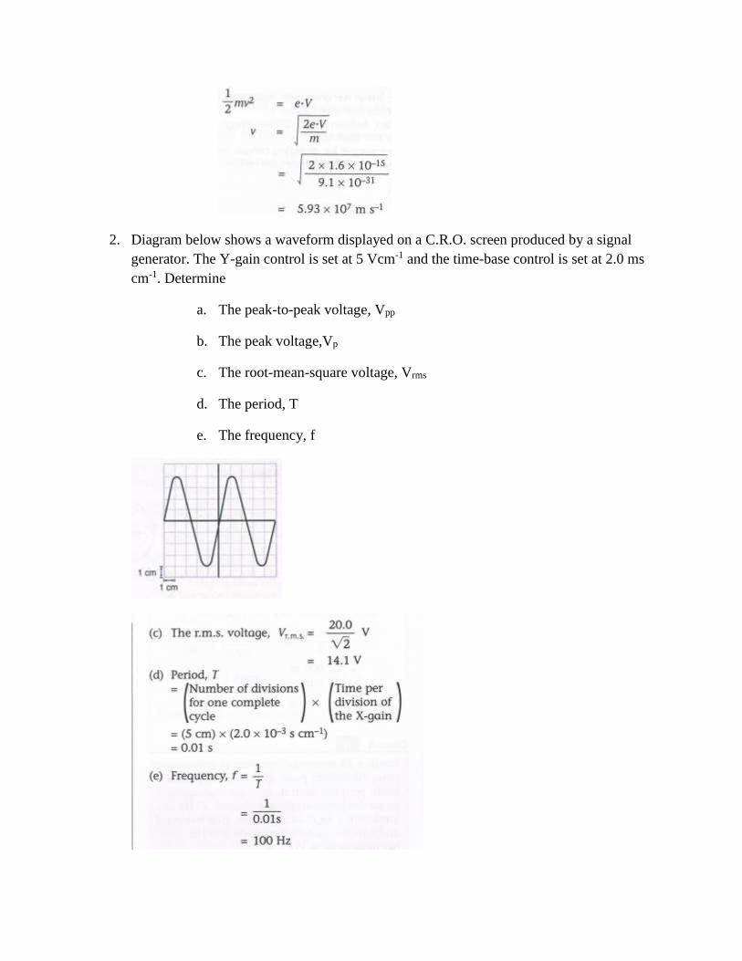
2. Diagram below shows a waveform displayed on a C.R.O. screen produced by a signal
generator. The Y-gain control is set at 5 Vcm-1 and the time-base control is set at 2.0 ms
cm-1. Determine
a. The peak-to-peak voltage, Vpp
b. The peak voltage,Vp
c. The root-mean-square voltage, Vrms
d. The period, T
e. The frequency, f
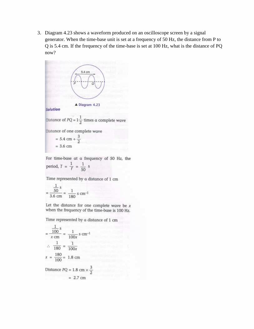
3. Diagram 4.23 shows a waveform produced on an oscilloscope screen by a signal
generator. When the time-base unit is set at a frequency of 50 Hz, the distance from P to
Q is 5.4 cm. If the frequency of the time-base is set at 100 Hz, what is the distance of PQ
now?
4.2. Semiconductor Diodes
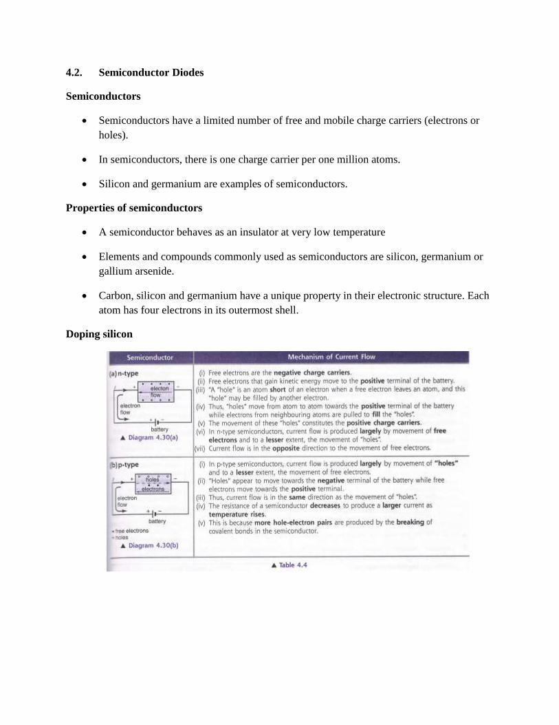
Semiconductors
Semiconductors have a limited number of free and mobile charge carriers (electrons or
holes).
In semiconductors, there is one charge carrier per one million atoms.
Silicon and germanium are examples of semiconductors.
Properties of semiconductors
A semiconductor behaves as an insulator at very low temperature
Elements and compounds commonly used as semiconductors are silicon, germanium or
gallium arsenide.
Carbon, silicon and germanium have a unique property in their electronic structure. Each
atom has four electrons in its outermost shell.
Doping silicon
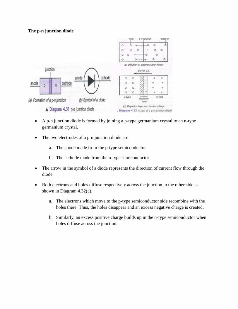
The p-n junction diode
A p-n junction diode is formed by joining a p-type germanium crystal to an n-type
germanium crystal.
The two electrodes of a p-n junction diode are :
a. The anode made from the p-type semiconductor
b. The cathode made from the n-type semiconductor
The arrow in the symbol of a diode represents the direction of current flow through the
diode.
Both electrons and holes diffuse respectively across the junction to the other side as
shown in Diagram 4.32(a).
a. The electrons which move to the p-type semiconductor side recombine with the
holes there. Thus, the holes disappear and an excess negative charge is created.
b. Similarly, an excess positive charge builds up in the n-type semiconductor when
holes diffuse across the junction.
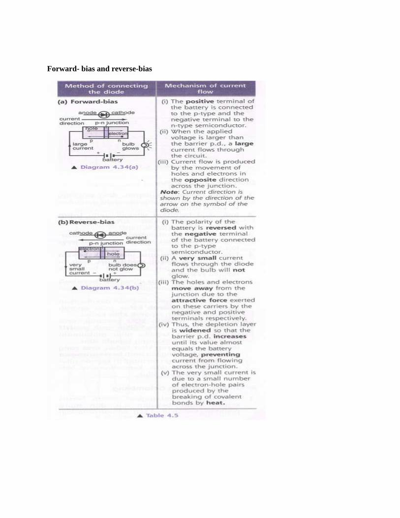
Forward- bias and reverse-bias
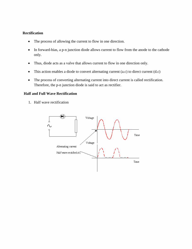
Rectification
The process of allowing the current to flow in one direction.
In forward-bias, a p-n junction diode allows current to flow from the anode to the cathode
only.
Thus, diode acts as a valve that allows current to flow in one direction only.
This action enables a diode to convert alternating current (a.c) to direct current (d.c)
The process of converting alternating current into direct current is called rectification.
Therefore, the p-n junction diode is said to act as rectifier.
Half and Full Wave Rectification
1. Half wave rectification
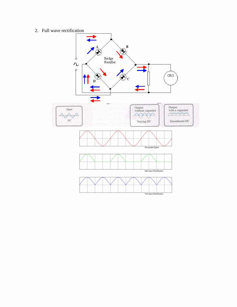
2. Full wave rectification
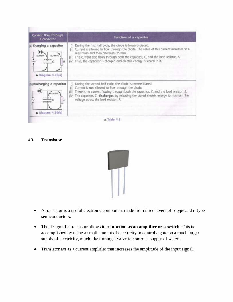
4.3. Transistor
A transistor is a useful electronic component made from three layers of p-type and n-type
semiconductors.
The design of a transistor allows it to function as an amplifier or a switch. This is
accomplished by using a small amount of electricity to control a gate on a much larger
supply of electricity, much like turning a valve to control a supply of water.
Transistor act as a current amplifier that increases the amplitude of the input signal.
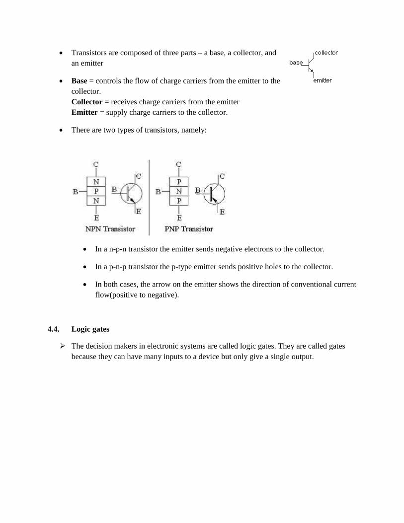
Transistors are composed of three parts – a base, a collector, and
an emitter
Base = controls the flow of charge carriers from the emitter to the
collector.
Collector = receives charge carriers from the emitter
Emitter = supply charge carriers to the collector.
There are two types of transistors, namely:
In a n-p-n transistor the emitter sends negative electrons to the collector.
In a p-n-p transistor the p-type emitter sends positive holes to the collector.
In both cases, the arrow on the emitter shows the direction of conventional current
flow(positive to negative).
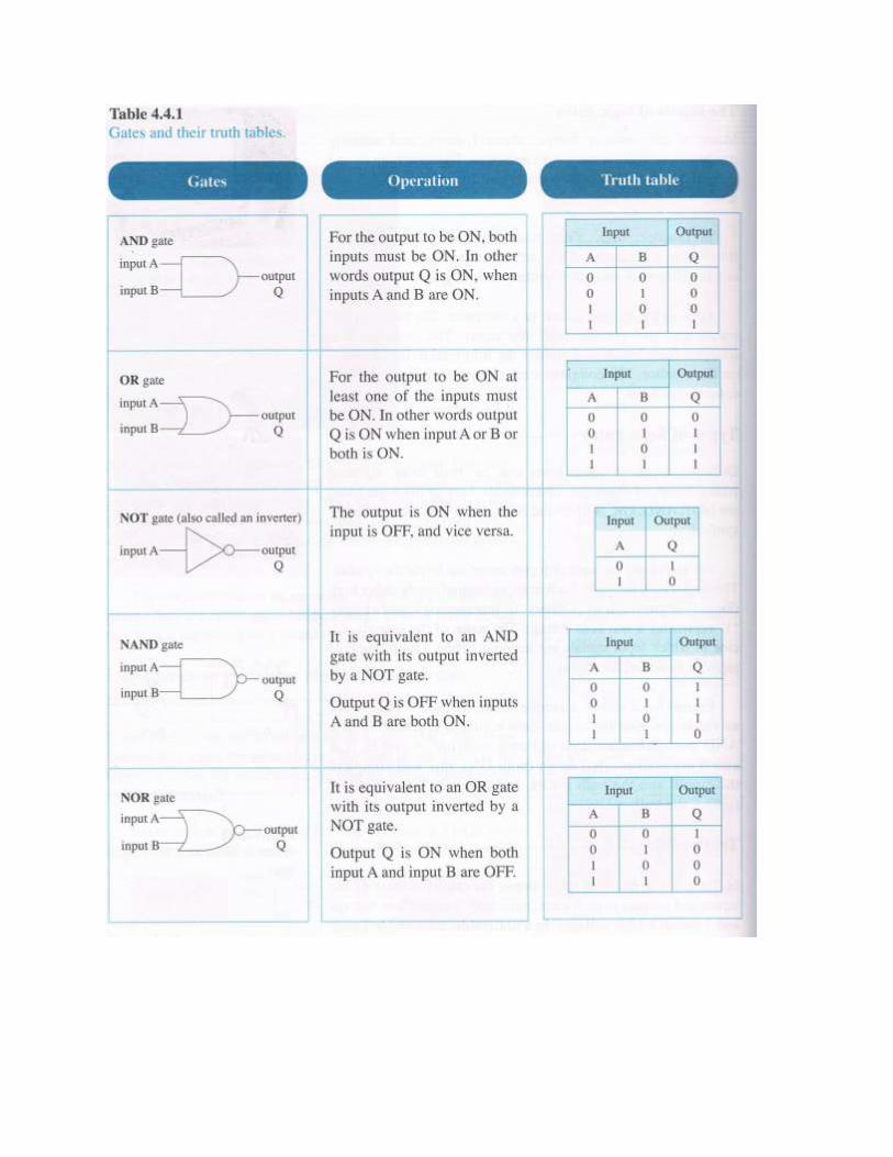
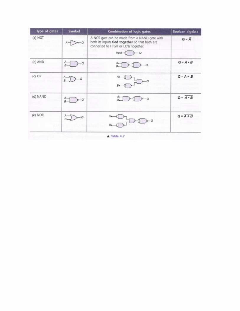
4.4. Logic gates
The decision makers in electronic systems are called logic gates. They are called gates
because they can have many inputs to a device but only give a single output.