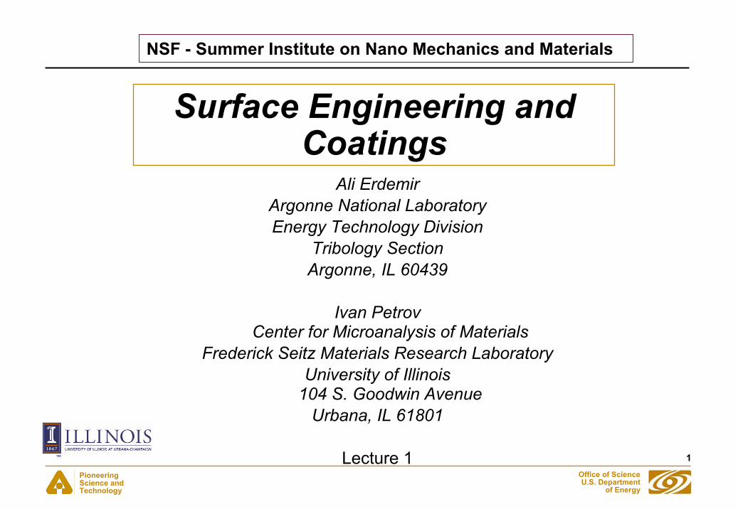
1
Pioneering Science andTechnology
Office of ScienceU.S. Department
of Energy
Ali ErdemirArgonne National LaboratoryEnergy Technology Division
Tribology SectionArgonne, IL 60439
Ivan Petrov Center for Microanalysis of Materials
Frederick Seitz Materials Research LaboratoryUniversity of Illinois
104 S. Goodwin AvenueUrbana, IL 61801
Lecture 1
NSF - Summer Institute on Nano Mechanics and Materials
Surface Engineering and Coatings
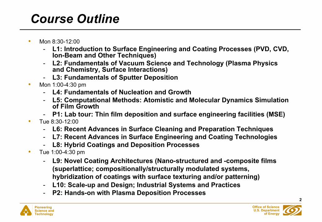
2
Pioneering Science andTechnology
Office of ScienceU.S. Department
of Energy
Course Outline• Mon 8:30-12:00
- L1: Introduction to Surface Engineering and Coating Processes (PVD, CVD, Ion-Beam and Other Techniques)
- L2: Fundamentals of Vacuum Science and Technology (Plasma Physics and Chemistry, Surface Interactions)
- L3: Fundamentals of Sputter Deposition • Mon 1:00-4:30 pm
- L4: Fundamentals of Nucleation and Growth - L5: Computational Methods: Atomistic and Molecular Dynamics Simulation
of Film Growth - P1: Lab tour: Thin film deposition and surface engineering facilities (MSE)
• Tue 8:30-12:00- L6: Recent Advances in Surface Cleaning and Preparation Techniques - L7: Recent Advances in Surface Engineering and Coating Technologies- L8: Hybrid Coatings and Deposition Processes
• Tue 1:00-4:30 pm- L9: Novel Coating Architectures (Nano-structured and -composite films
(superlattice; compositionally/structurally modulated systems, hybridization of coatings with surface texturing and/or patterning)
- L10: Scale-up and Design; Industrial Systems and Practices - P2: Hands-on with Plasma Deposition Processes

3
Pioneering Science andTechnology
Office of ScienceU.S. Department
of Energy
Outline Cont’d
• Wed 8:30-12:00 - L11: Introduction to Thin Film Characterization - L12: Surface Characterization (physical and chemical methods, XPS,
AES, SIMS, etc)- L13: Structural Characterization (TEM, SEM, etc.)
• Wed 1:00-4:30 pm- L14: Mechanical Characterization (Adhesion, Hardness, Elastic
Properties, Toughness, etc.) - P3: Lab Tour: Surface and Structural Characterization Facilities- P4: Practical Experience with Some of the Characterization Methods
(SEM, TEM, AFM, etc.)• Thu 8:30-12:00
- L15: Tribological Characterization- L15: An Overview of Emerging Technologies- L16: Superhardness and superlubricity: theory and experiments
• Thu 1:00-4:30 pm- L17: Classification and Industrial Applications of Coatings- P4: Lab Tour: Tribology Test Facilities (ME)- P5: Hands-on Nano-indentation, Tribology

4
Pioneering Science andTechnology
Office of ScienceU.S. Department
of Energy
Outline Cont’d
• Fri 8:30-12:00
- L18: Guest Speaker 1: Dr. K. Wahl, NRLNanomechanics and tribology of coatings
- L19: Guest Speaker 2: Prof. Y.-W. Chung, NSF.Applications of Tribological Coatings in Extremely High-Density Computer Disk Drive Applications
- L20: Guest Speaker: Dr. Jeffrey Sanders, AFRL/MLBTAdvanced Materials and Coatings for Aerospace Applications
• Tentative Lab Tours
- Material Science & Engineering - Mechanical Engineering- NUANCE Microscopy Facility- Surface Electron & X-Ray Diffraction

5
Pioneering Science andTechnology
Office of ScienceU.S. Department
of Energy
L1: INTRODUCTION TO SURFACE ENGINEERING AND COATING
PROCESSES
6
Pioneering Science andTechnology
Office of ScienceU.S. Department
of Energy
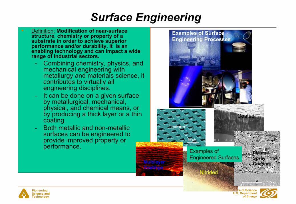
Surface Engineering• Definition: Modification of near-surface
structure, chemistry or property of a substrate in order to achieve superior performance and/or durability. It is an enabling technology and can impact a wide range of industrial sectors.- Combining chemistry, physics, and
mechanical engineering with metallurgy and materials science, it contributes to virtually all engineering disciplines.
- It can be done on a given surface by metallurgical, mechanical, physical, and chemical means, or by producing a thick layer or a thin coating.
- Both metallic and non-metallic surfaces can be engineered to provide improved property or performance.
Examples of SurfaceEngineering Processes
Textured
Nitrided
Coated
MultilayerCoatings
Examples of Engineered Surfaces
PlasmaSprayCoating
7
Pioneering Science andTechnology
Office of ScienceU.S. Department
of Energy
What are the benefits and where are they used? • Specific properties rely on surfaces
- Wear, friction, corrosion, fatigue, reflectivity, emissivity, color, thermal/electrical conductivity, bio-compatibility, etc.
• Benefits- Extend product life (durability)- Improve resistance to wear, oxidation and corrosion
(performance)- Satisfy the consumer's need for better and lower cost
components- Reduce maintenance (reliability and cost)- Reduce emissions and environmental waste- Improve the appearance; visually attractivity- Improve electrical conductivity- Improve solderability- Metallize plastic component surfaces - Provide shielding for electromagnetic and radio frequency
radiation. • By improving durability, it reduces waste of natural
resources and energy. • Surface engineered automotive parts and components
can extend warranties and reduce emissions. For example: A hardened engine valve will last a minimum of five years without replacement.
Cutting
Forming
Automotive
Decoration
Bio-medical
8
Pioneering Science andTechnology
Office of ScienceU.S. Department
of Energy
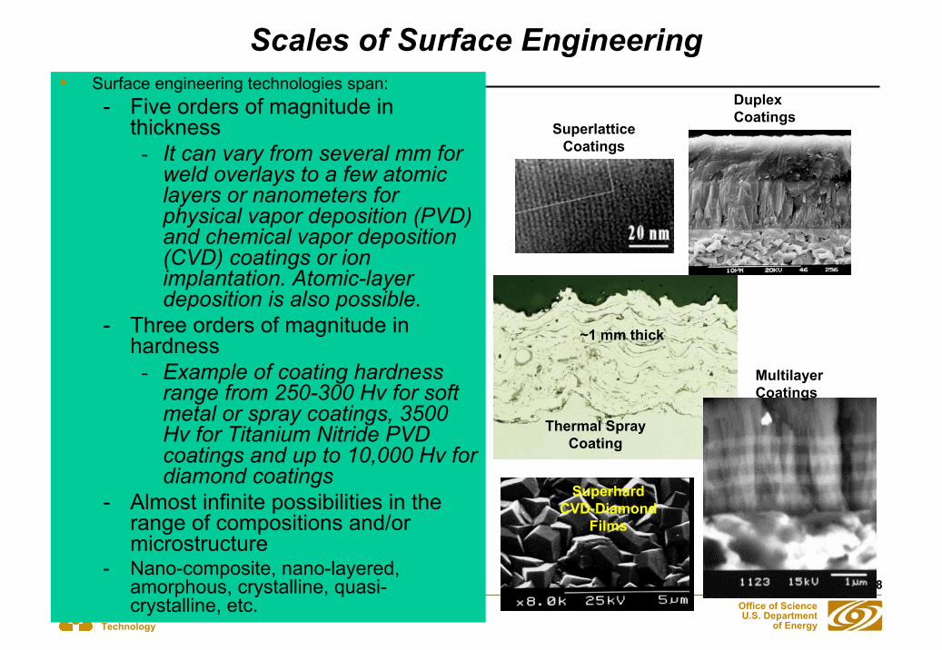
Scales of Surface Engineering• Surface engineering technologies span:
- Five orders of magnitude in thickness- It can vary from several mm for
weld overlays to a few atomic layers or nanometers for physical vapor deposition (PVD) and chemical vapor deposition (CVD) coatings or ion implantation. Atomic-layer deposition is also possible.
- Three orders of magnitude in hardness - Example of coating hardness
range from 250-300 Hv for soft metal or spray coatings, 3500 Hv for Titanium Nitride PVD coatings and up to 10,000 Hv for diamond coatings
- Almost infinite possibilities in the range of compositions and/or microstructure
- Nano-composite, nano-layered, amorphous, crystalline, quasi-crystalline, etc.
SuperlatticeCoatings
DuplexCoatings
Thermal SprayCoating
MultilayerCoatings
SuperhardCVD-Diamond
Films
~1 mm thick

9
Pioneering Science andTechnology
Office of ScienceU.S. Department
of Energy
Evolution and Significance of Surface Engineering
- It is an enabling technology- It can combine various surface
treatments with thin film and coating deposition.
- It can substantially improve wear and corrosion resistance of structural components.
- It increases component lifetime and resistance to aggressive environments.
- It can produce functional coatings that modify biocompatibility and optical and electrical properties of critical components
Evolution of Coating
Architectures Nanostructured,Superlattice, Gradient
Multicomponent, Multilayer
Single component
Adaptative (smart)
(1980s)
(1990s)
(2000 and beyond)

10
Pioneering Science andTechnology
Office of ScienceU.S. Department
of Energy
Classification of Surface Engineering Processes
• The traditional, well established processes:
- Painting- Electroplating- Galvanizing- Thermal and plasma spraying- Nitriding. Carburizing, Boriding
• The more technologically advanced coating technologies:
- Physical and chemical vapor deposition
- Ion implantation- Ion-assisted deposition- Ion-beam mixing- Laser treatment
• Nowadays, a multitude of options are available to select and specify a treatment or a combination of treatments to engineer the surfaces of components or structures.
Plasma Spray
PlasmaNitriding
Ion-beamdeposition
CVD
PVD
Plasma-sourceIon Implantation
11
Pioneering Science andTechnology
Office of ScienceU.S. Department
of Energy
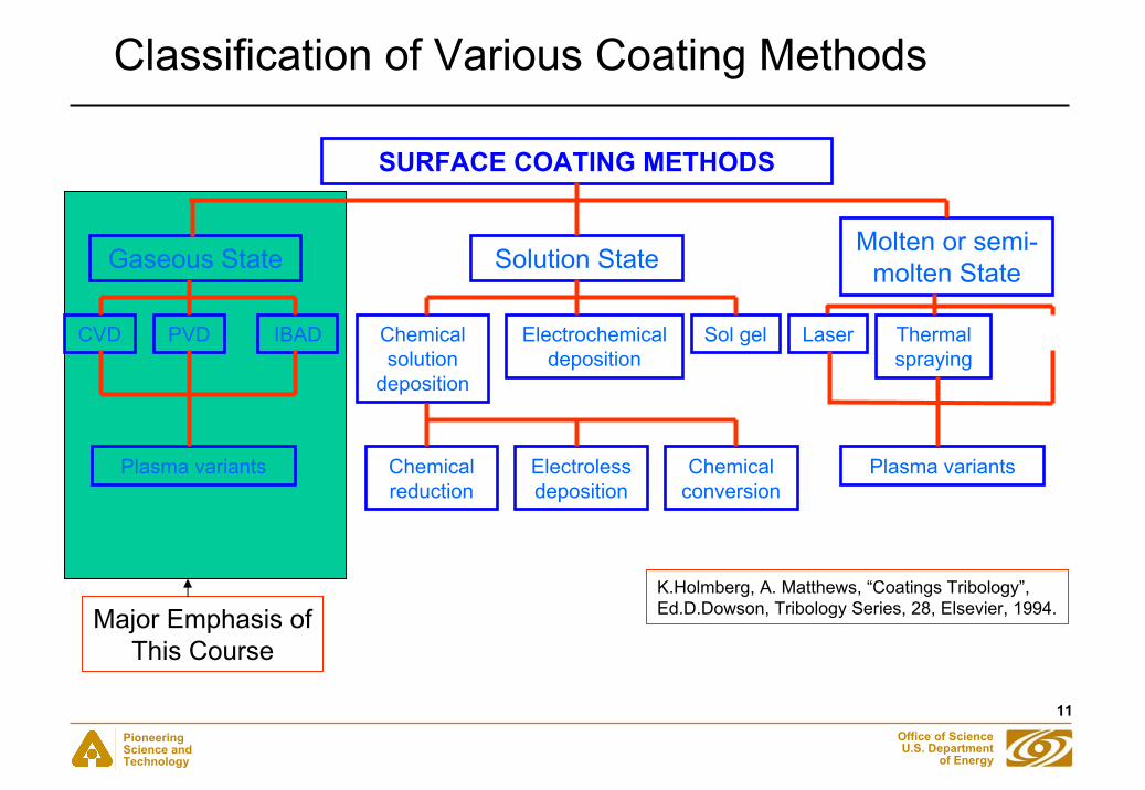
Classification of Various Coating Methods
SURFACE COATING METHODS
Gaseous State Solution StateMolten or semi-
molten State
CVD PVD IBAD Chemical solution
deposition
Electrochemical deposition
Sol gel Laser Thermal spraying
Plasma variants Chemical reduction
Electrolessdeposition
Chemical conversion
Plasma variants
K.Holmberg, A. Matthews, “Coatings Tribology”, Ed.D.Dowson, Tribology Series, 28, Elsevier, 1994.Major Emphasis of
This Course
12
Pioneering Science andTechnology
Office of ScienceU.S. Department
of Energy
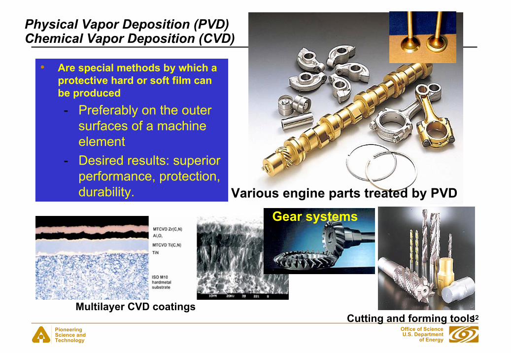
Physical Vapor Deposition (PVD)Chemical Vapor Deposition (CVD)
• Are special methods by which a protective hard or soft film can be produced- Preferably on the outer
surfaces of a machine element
- Desired results: superior performance, protection, durability. Various engine parts treated by PVD
Cutting and forming tools
Gear systems
Multilayer CVD coatings
13
Pioneering Science andTechnology
Office of ScienceU.S. Department
of Energy
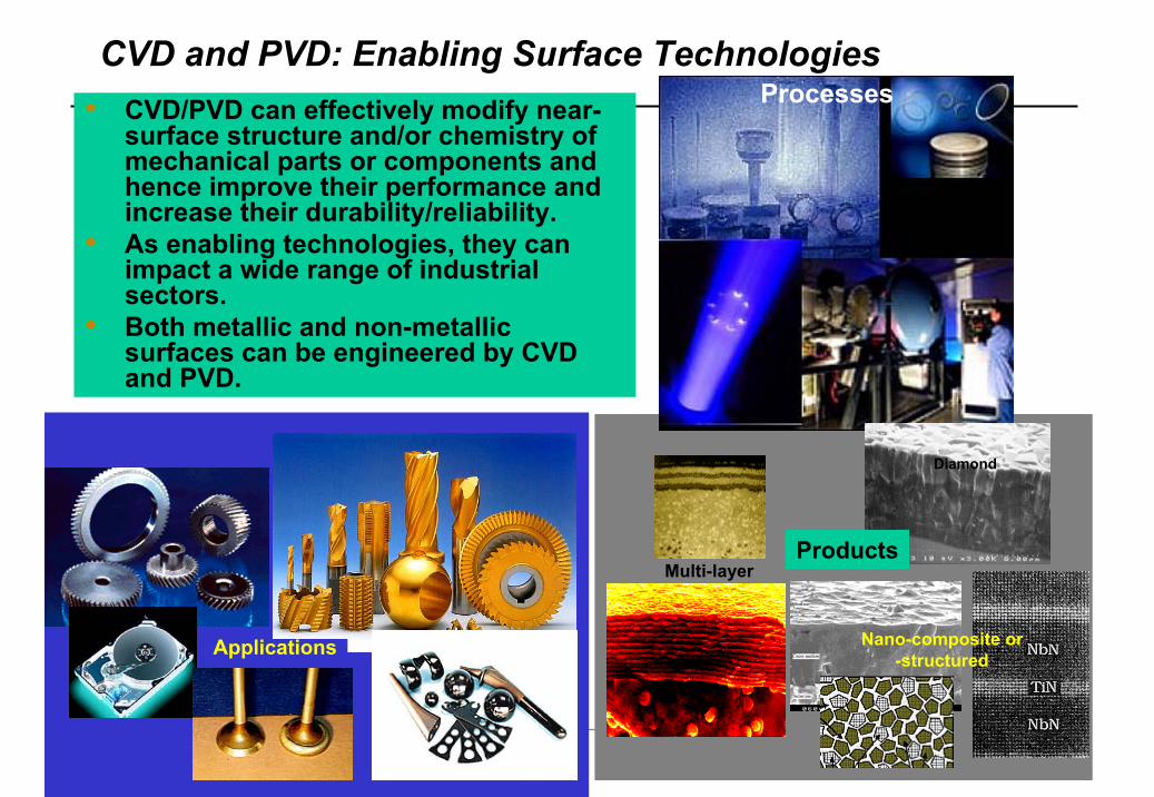
CVD and PVD: Enabling Surface Technologies• CVD/PVD can effectively modify near-
surface structure and/or chemistry of mechanical parts or components and hence improve their performance and increase their durability/reliability.
• As enabling technologies, they can impact a wide range of industrial sectors.
• Both metallic and non-metallic surfaces can be engineered by CVD and PVD.
Processes
Multi-layer
Diamond
Products
Applications Nano-composite or-structured
14
Pioneering Science andTechnology
Office of ScienceU.S. Department
of Energy
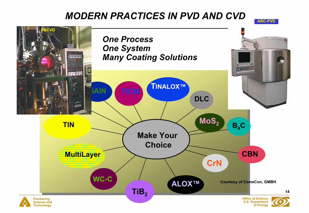
MODERN PRACTICES IN PVD AND CVDARC-PVD
cc
CCplusCTiAlN TiCN
CrN
TiB2
WC-C
B4CMoS2
Make Your Choice
CBN
DLC
TINALOX™
TIN
ALOX™
MultiLayer
One Process One System Many Coating Solutions
PACVD
Courtesy of CemeCon, GMBH
15
Pioneering Science andTechnology
Office of ScienceU.S. Department
of Energy
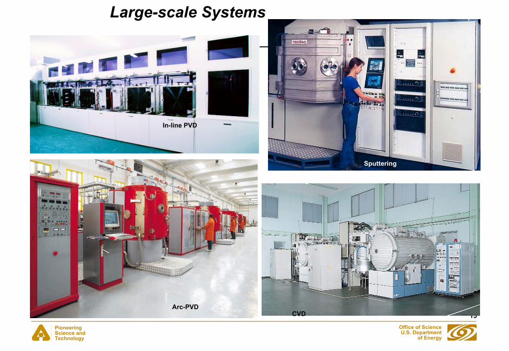
Arc-PVD
In-line PVD
CVD
Sputtering
Large-scale Systems
16
Pioneering Science andTechnology
Office of ScienceU.S. Department
of Energy
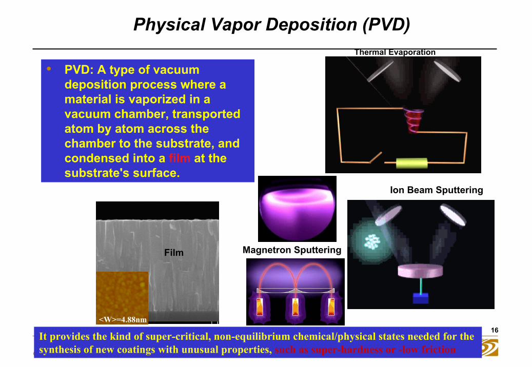
Physical Vapor Deposition (PVD)
• PVD: A type of vacuum deposition process where a material is vaporized in a vacuum chamber, transported atom by atom across the chamber to the substrate, and condensed into a film at the substrate's surface.
Thermal Evaporation
Ion Beam Sputtering
Magnetron Sputtering
<W>=4.88nm
Film
It provides the kind of super-critical, non-equilibrium chemical/physical states needed for the synthesis of new coatings with unusual properties, such as super-hardness or -low friction
17
Pioneering Science andTechnology
Office of ScienceU.S. Department
of Energy
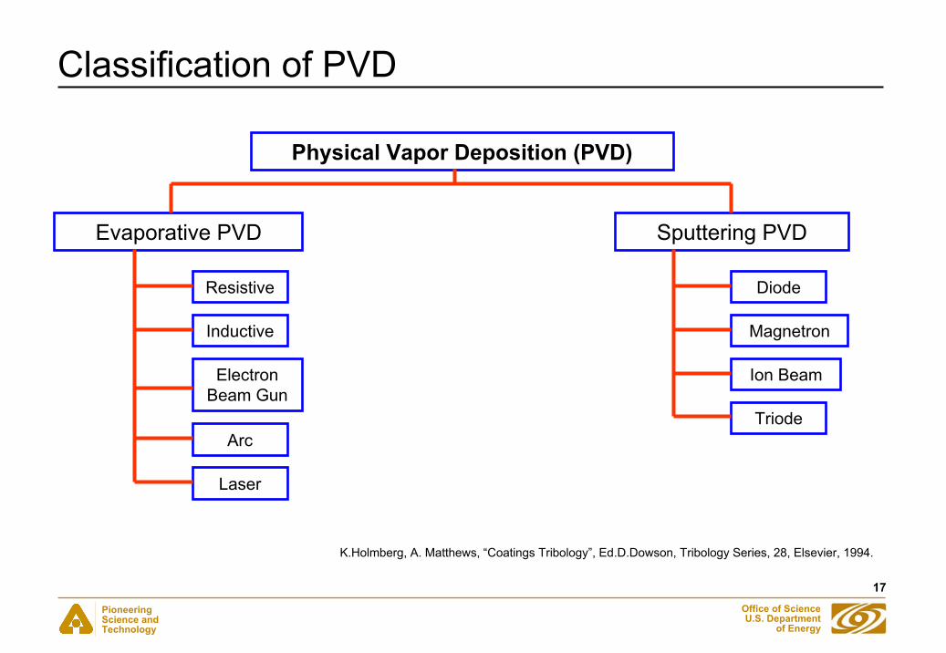
Classification of PVD
Physical Vapor Deposition (PVD)
Evaporative PVD Sputtering PVD
Resistive
Inductive
Electron Beam Gun
Arc
Laser
Diode
Magnetron
Ion Beam
Triode
K.Holmberg, A. Matthews, “Coatings Tribology”, Ed.D.Dowson, Tribology Series, 28, Elsevier, 1994.
18
Pioneering Science andTechnology
Office of ScienceU.S. Department
of Energy
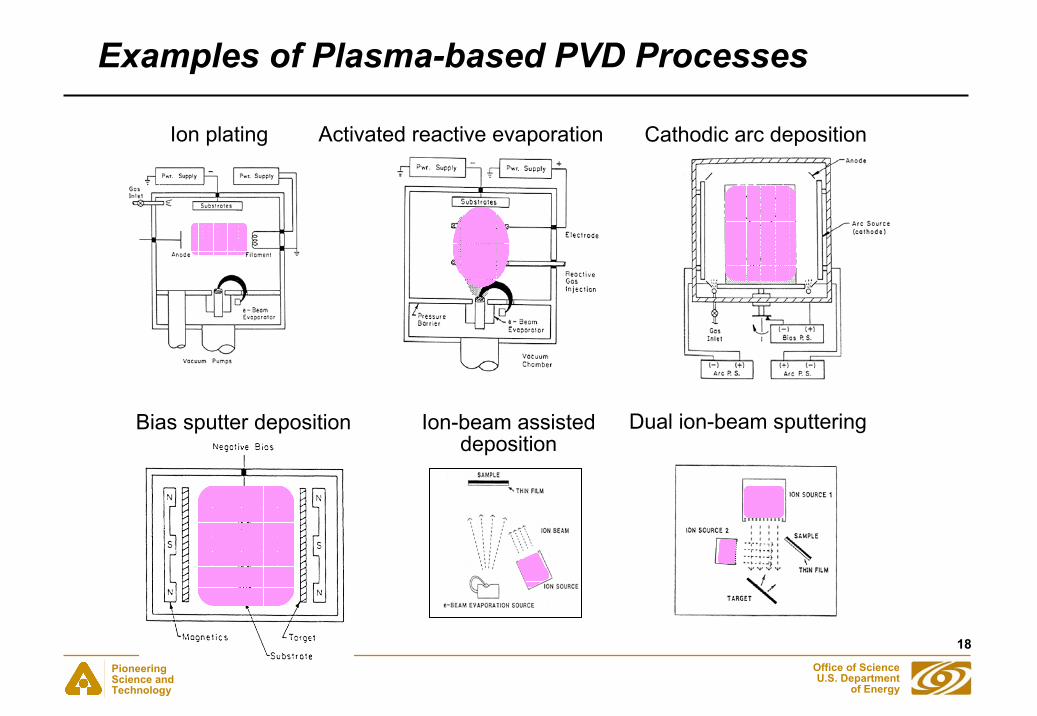
Examples of Plasma-based PVD Processes
Activated reactive evaporation Cathodic arc deposition
Bias sputter deposition Ion-beam assisteddeposition
Dual ion-beam sputtering
Ion plating
19
Pioneering Science andTechnology
Office of ScienceU.S. Department
of Energy
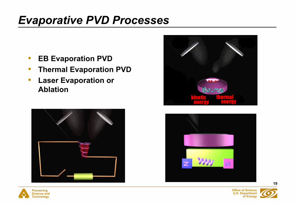
Evaporative PVD Processes
• EB Evaporation PVD• Thermal Evaporation PVD• Laser Evaporation or
Ablation

20
Pioneering Science andTechnology
Office of ScienceU.S. Department
of Energy
Sputter DepositionBasics:
• A voltage is applied across a rarified gas.• Breakdown of the gas forms a glow
discharge plasma.• Positive ions from the plasma strike the
negative electrode. • Energy from the ions is transferred to
target atoms. • A few of these may escape from the
target surface (they are sputtered).• The sputtered atoms condense on the
substrate forming a film.
Magnetron: a device in which a magnet systemon the back of the cathode deflects the electrons, thus lengthening the ionization path. The accelerated ions transfer their momentum to particles of the coating material, which are then deposited on the substrate.
Magnetron

21
Pioneering Science andTechnology
Office of ScienceU.S. Department
of Energy
• Cold Cathode DC Diode sputtering
• DC triode Sputtering• AC Sputtering• Rf Sputtering• DC Magnetron Sputtering
- Unbalanced Magnetron- Balanced Magnetron- Pulsed DC Magnetron- Ion and Plasma Beam
Sputtering
Ion-beam sputtering
Schematic representationVarious Sputtering Methods

22
Pioneering Science andTechnology
Office of ScienceU.S. Department
of Energy
Sputtering Mechanism
•Bombardment of solid (target) by high energy chemically inert ions (e.g. Ar+)That are extracted from plasma.
•Such bombardment causes ejection of atoms from the target which are then re-deposited on the surface of the substrate purposely located in the vicinity of the target.

23
Pioneering Science andTechnology
Office of ScienceU.S. Department
of Energy
Diode vs Magnetron Sputtering
•Comments: •Simple, relative ease in fabrication and thickness uniformity over large area •Realtively high deposition pressure and relatively high substrate temperature
Comments: •High deposition rates, low deposition pressure, low substrate temperature, can be scaled up, so commonly used for industrial production •More complex than planar diode systems
Diode
Magnetron
24
Pioneering Science andTechnology
Office of ScienceU.S. Department
of Energy
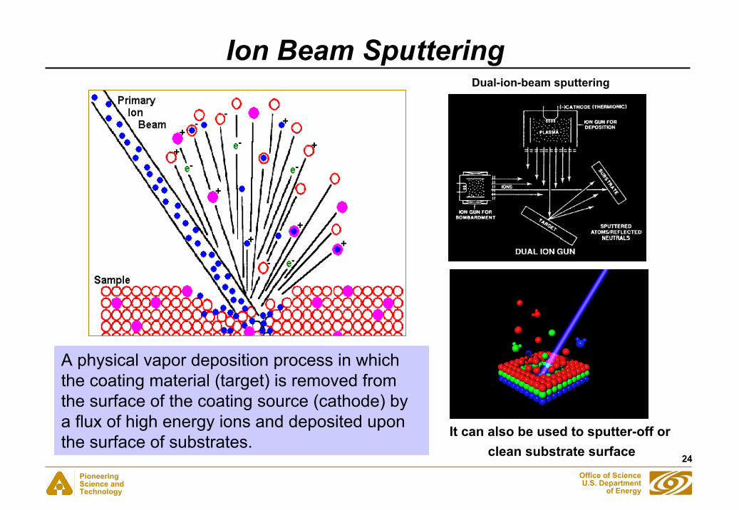
Ion Beam Sputtering
A physical vapor deposition process in which the coating material (target) is removed from the surface of the coating source (cathode) by a flux of high energy ions and deposited upon the surface of substrates.
It can also be used to sputter-off or clean substrate surface
Dual-ion-beam sputtering
25
Pioneering Science andTechnology
Office of ScienceU.S. Department
of Energy
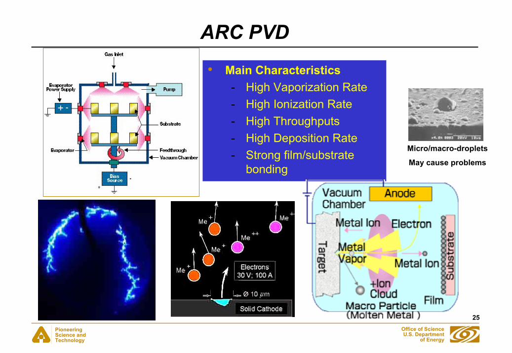
ARC PVD
• Main Characteristics- High Vaporization Rate- High Ionization Rate- High Throughputs- High Deposition Rate- Strong film/substrate
bonding
Micro/macro-droplets
May cause problems
26
Pioneering Science andTechnology
Office of ScienceU.S. Department
of Energy
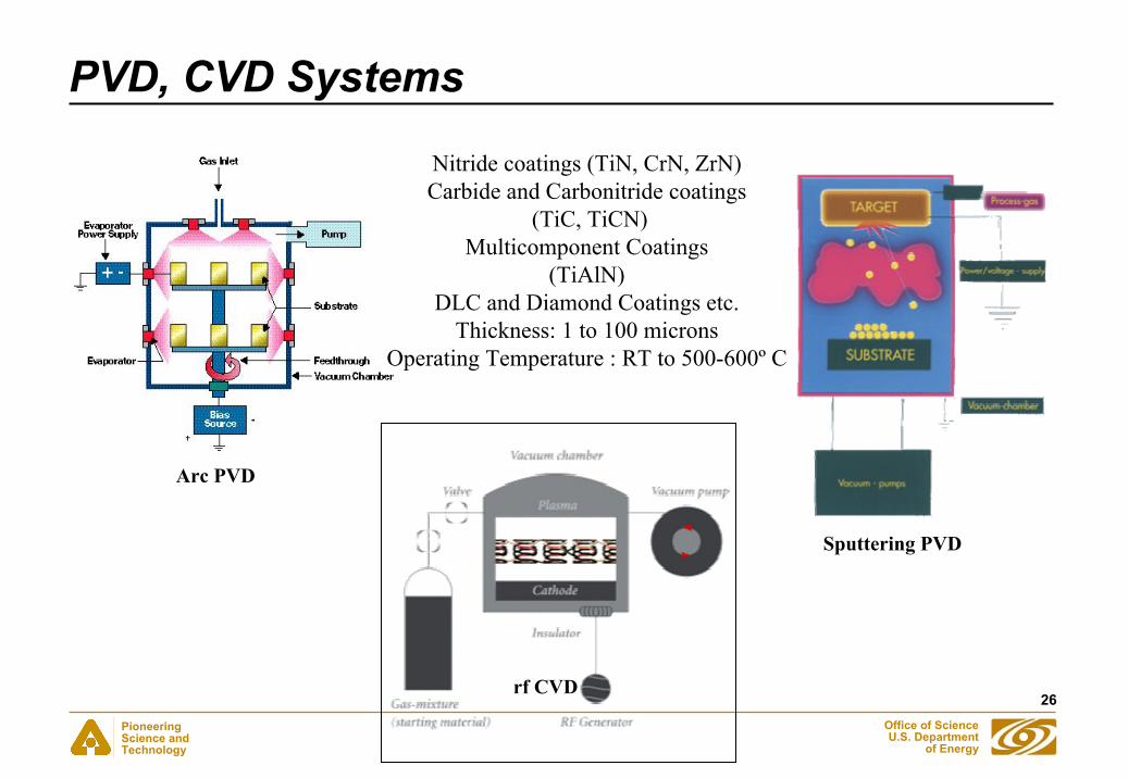
PVD, CVD Systems
Nitride coatings (TiN, CrN, ZrN)Carbide and Carbonitride coatings
(TiC, TiCN)Multicomponent Coatings
(TiAlN)DLC and Diamond Coatings etc.
Thickness: 1 to 100 micronsOperating Temperature : RT to 500-600º C
Arc PVD
rf CVD
Sputtering PVD
27
Pioneering Science andTechnology
Office of ScienceU.S. Department
of Energy
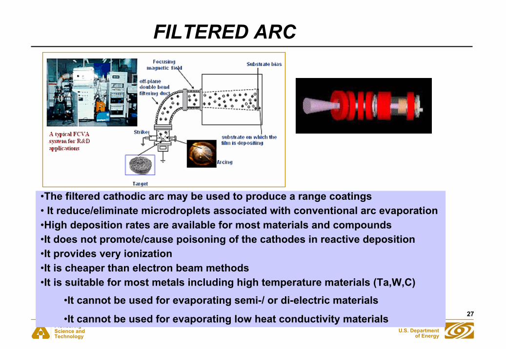
FILTERED ARC
•The filtered cathodic arc may be used to produce a range coatings• It reduce/eliminate microdroplets associated with conventional arc evaporation •High deposition rates are available for most materials and compounds•It does not promote/cause poisoning of the cathodes in reactive deposition•It provides very ionization •It is cheaper than electron beam methods•It is suitable for most metals including high temperature materials (Ta,W,C)
•It cannot be used for evaporating semi-/ or di-electric materials
•It cannot be used for evaporating low heat conductivity materials
28
Pioneering Science andTechnology
Office of ScienceU.S. Department
of Energy
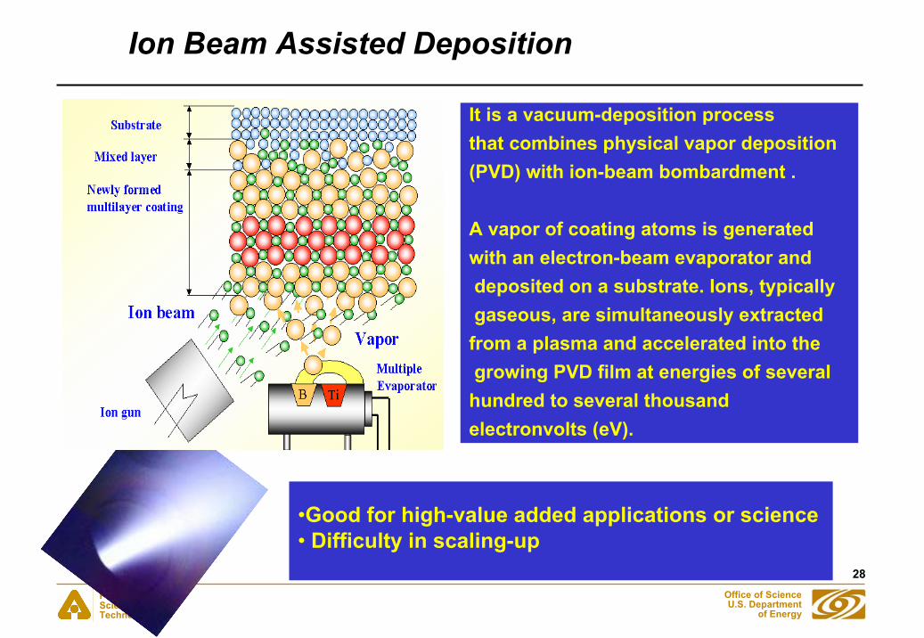
Ion Beam Assisted Deposition
It is a vacuum-deposition process that combines physical vapor deposition (PVD) with ion-beam bombardment .
A vapor of coating atoms is generated with an electron-beam evaporator anddeposited on a substrate. Ions, typicallygaseous, are simultaneously extracted from a plasma and accelerated into thegrowing PVD film at energies of several hundred to several thousand electronvolts (eV).
•Good for high-value added applications or science • Difficulty in scaling-up
29
Pioneering Science andTechnology
Office of ScienceU.S. Department
of Energy
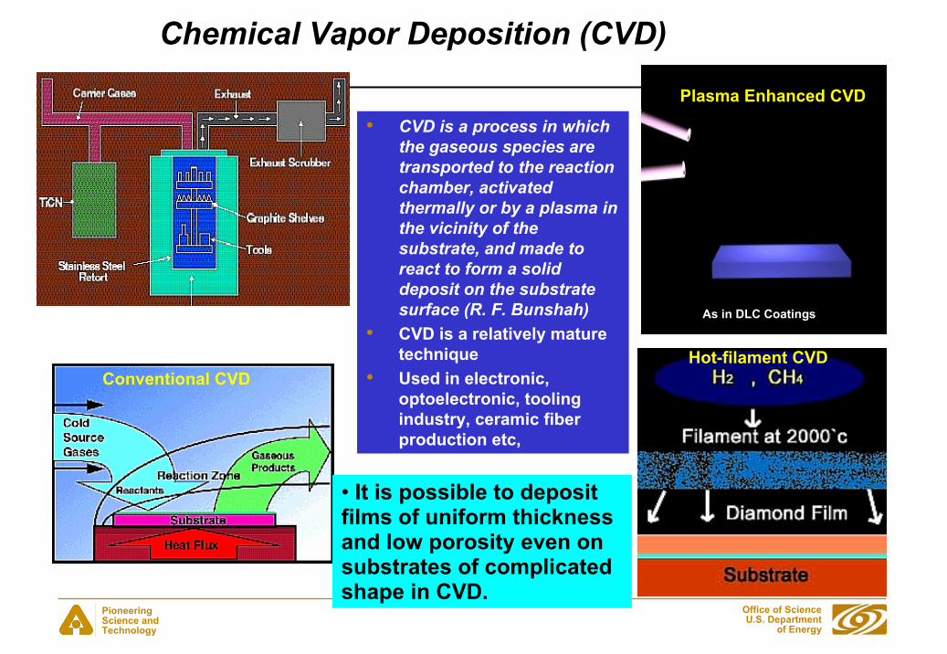
Chemical Vapor Deposition (CVD)
• CVD is a process in which the gaseous species are transported to the reaction chamber, activated thermally or by a plasma in the vicinity of the substrate, and made to react to form a solid deposit on the substrate surface (R. F. Bunshah)
• CVD is a relatively mature technique
• Used in electronic, optoelectronic, tooling industry, ceramic fiber production etc,
• It is possible to deposit films of uniform thickness and low porosity even on substrates of complicated shape in CVD.
Conventional CVD
Plasma Enhanced CVD
Hot-filament CVD
As in DLC Coatings
30
Pioneering Science andTechnology
Office of ScienceU.S. Department
of Energy
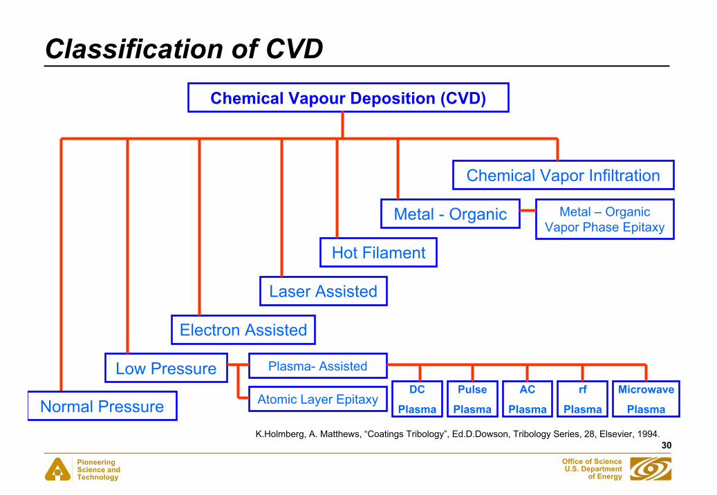
Classification of CVDChemical Vapour Deposition (CVD)
Chemical Vapor Infiltration
Metal - Organic
Hot Filament
Laser Assisted
Electron Assisted
Low Pressure
Normal Pressure
Metal – Organic Vapor Phase Epitaxy
Plasma- Assisted
Atomic Layer EpitaxyDC
Plasma
Pulse
Plasma
AC
Plasma
rf
Plasma
Microwave
Plasma
K.Holmberg, A. Matthews, “Coatings Tribology”, Ed.D.Dowson, Tribology Series, 28, Elsevier, 1994.

31
Pioneering Science andTechnology
Office of ScienceU.S. Department
of Energy
The Gas-Phase Chemistry of CVD Processes
• Thermal-Decomposition Reactions:- Hydrocarbon Decomposition CH4(g) → C(s)+2H2(g)- Halide Decomposition WF6(g) → W(s)+3F6(g)- Carbonyl Decomposition Ni(CO)4(g) → Ni(s)+4CO(g)- Hydride Decomposition SiH4(g) → Si(s)+2H2(g)
• Hydrogen Reduction:SiCl4(g)+2H2(g) → Si(s)+4HCl(g)
• Co-reduction:TiCl4(g)+2BCl3(g)+5H2(g) → TiB2(s)+10HCl(g)
• Reactions Leading to Carbide and Nitride Formation:TiCl4(g)+CH4(g) → TiC(s)+4HCl(g)3SiCl4(g)+4NH3(g) → Si3N4(s)+12HCl(g)
CVD TiN and TiC Coated Tool Inserts
CVD is able to produce single or multilayer coatings with composite or nanostructuredarchitectures. It is not a line of sight process, hence allows the coating of complex shaped engineering components. Major drawbacks: Safety issue (hazardous, flammable gases), high-temperature requirement.

32
Pioneering Science andTechnology
Office of ScienceU.S. Department
of Energy
Example of Plasma Assisted CVD
Hot-filament CVD
Plasma-enhanced CVD
Chemical/Physical Events That Control Nucleation
and Growth
Used inDepositionOf DLC
33
Pioneering Science andTechnology
Office of ScienceU.S. Department
of Energy
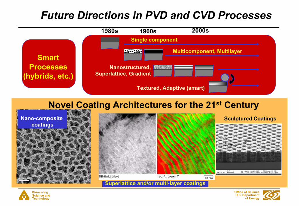
Future Directions in PVD and CVD Processes
SmartProcesses
(hybrids, etc.)Nanostructured,
Superlattice, Gradient
Multicomponent, Multilayer
Single component
Textured, Adaptive (smart)
Nano-composite coatings
Superlattice and/or multi-layer coatings
Sculptured Coatings
1980s 1900s 2000s
Novel Coating Architectures for the 21st Century
34
Pioneering Science andTechnology
Office of ScienceU.S. Department
of Energy
Key References• ASM Handbook: Surface Engineering, by Faith Reidenback, ASM-International,
Metals Park, OH, 1994• Surface Engineering: Fundamentals of Coatings by P. K. Datta and J. S. Gray,
Royal Society of Chemistry, 1993• Chemical Vapor Deposition (Surface Engineering Series, V. 2)
by J.-H. Park and T. S. Sudarshan, ASM-International, Metals Park OH, 2001.• Chemical vapour deposition of coatings by K.L. Choy, Progress in Materials
Science, 48 (2003) 57–170.• Advanced Surface Coatings: A Handbook of Surface Engineering, by D. S.
Rickerby, A. Mathews, Blackie Academic and Professional Publ. 1991.• Handbook of Hard Coatings, by R. F. Bunshah, William Andrew
Publishing/Noyes, 2001.• Handbook of Physical Vapor Deposition (PVD) Processing by
D. M. Mattox, William Andrew Publishing/Noyes, 1998. • Handbook of Thin-Film Deposition Processes and Techniques - Principles,
Methods, Equipment and Applications, by K. Seshan, William Andrew Publishing/Noyes, 2002.
Recommended


![In vivo micro medical devices [Recovered]tam.northwestern.edu/summerinstitute/_links/_courses/2007... · • 1967, Ko, W. H and NeumanMR, “Implant Biotelemetry and Microelectronics”Science](https://img.pdfslide.us/doc/110x75/5c07470509d3f2922c8b5bdd/in-vivo-micro-medical-devices-recoveredtam-1967-ko-w-h-and-neumanmr.jpg)