Embed Size (px)
Citation preview

Department of Materials Science and Engineering, Northwestern University
Probing Molecular Electronics withScanning Probe Microscopy
Department of Materials Science and Engineering,Northwestern University, Evanston, IL 60208-3108
Ph: 847-491-2696, [email protected]: http://www.hersam-group.northwestern.edu/
MarkMark C. HersamC. HersamAssistant ProfessorAssistant Professor

Department of Materials Science and Engineering, Northwestern University
Outline
• Motivation
• Background
• Construction
• SPM Techniques

Department of Materials Science and Engineering, Northwestern University
An Ideal Experiment forProbing Molecular Conduction
M. C. Hersam, et al., MRS Bulletin, 29, 385 (2004).

Department of Materials Science and Engineering, Northwestern University
Real Experimental Strategies forProbing Molecular Conduction
B. A. Mantooth, et al.,Proc. IEEE, 91, 1785 (2003).

Department of Materials Science and Engineering, Northwestern University
The Origin of Scanning Probe Microscopy
C. Julian Chen, Introduction to Scanning Tunneling Microscopy

Department of Materials Science and Engineering, Northwestern University
The Scanning Tunneling Microscope
• STM invented by Gerd Binnig and Heinrich Rohrer in 1982• Led to Nobel Prize in Physics, 1986
C. Julian Chen, Introduction to Scanning Tunneling Microscopy

Department of Materials Science and Engineering, Northwestern University
320 Å × 360 Å Step height ~ 12 Å
Si(111)-7×7: “Stairway to Heaven”
C. Julian Chen, Introduction to Scanning Tunneling Microscopy

Department of Materials Science and Engineering, Northwestern University
Scanning Tunneling Microscope Schematic
C. Julian Chen, Introduction to Scanning Tunneling Microscopy
Department of Materials Science and Engineering, Northwestern University
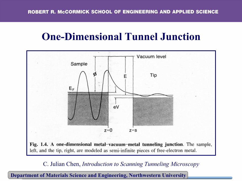
One-Dimensional Tunnel Junction
C. Julian Chen, Introduction to Scanning Tunneling Microscopy

Department of Materials Science and Engineering, Northwestern University
Tunneling Current – Approach #1
Assume metal-vacuum-metal junction, solve Schrödinger Equation:
I = tunneling current ρs = local density of states of sampleV = tip-sample voltage W = width of barrier
kWseVI 2−∝ ρ )(51.0
2eV
mk ϕ
φ== Å-1, where
Typically, φ ~ 4 eV k ~ 1 Å-1
Current decays by e2 ~ 7.4 times per Å

Department of Materials Science and Engineering, Northwestern University
Bardeen Tunneling Theory
C. Julian Chen, Introduction to Scanning Tunneling Microscopy

Department of Materials Science and Engineering, Northwestern University
Tunneling Current – Approach #2
Consider overlap of wavefunctions from either side of barrier:
Using Fermi’s Golden Rule (assuming kT << energy resolutionof the measurement),
For a free electron metal tip, ρt is constant:
)( eVEdVdI
Fs −∝ ρ STM Spectroscopy
∫ ++−∝eV
FtFs dEeVEI0
)()( εερερ
sample tip

Department of Materials Science and Engineering, Northwestern University
Atomic Force Microscopy
• Invented at Stanford by Binnig and Quate in 1986
• Bring tip-mounted micromachined cantilever into contactor close proximity of the surface
• “Atomic forces” deflect cantilever and is detected with laserdeflection into a position sensitive photodiode
• Cantilever deflection is control signal for the feedback loop
• AFM can be done on “any surface” (i.e., conductive, insulating,semiconducting, biological, etc.) in “any environment” (i.e., air,vacuum, liquid, etc.)

Department of Materials Science and Engineering, Northwestern University
Atomic Force Microscope Cantilevers
C. Julian Chen, Introduction to Scanning Tunneling Microscopy

Department of Materials Science and Engineering, Northwestern University
Force Detection with Optical Beam Deflection
C. Julian Chen, Introduction to Scanning Tunneling Microscopy

Department of Materials Science and Engineering, Northwestern University
Fluid Cell for Atomic Force Microscopy
C. Julian Chen, Introduction to Scanning Tunneling Microscopy

Department of Materials Science and Engineering, Northwestern University
Example UHV STM Design
• Homebuilt STM in the Hersam lab at Northwestern University• STM is a modified Lyding scanner

Department of Materials Science and Engineering, Northwestern University
Scanner Construction: Piezotubes
Outer tube:0.650” OD0.570” ID
0.750” Long
Inner tube:0.375” OD0.315” ID
0.750” Long

Department of Materials Science and Engineering, Northwestern University
Scanner Construction: Base Plug
Front View Rear View

Department of Materials Science and Engineering, Northwestern University
Scanner Construction:Piezotubes Soldered into Base Plug

Department of Materials Science and Engineering, Northwestern University
Scanner Construction:Course Translation Platform

Department of Materials Science and Engineering, Northwestern University
Scanner Construction:Course Translation Platform
Soldered onto Outer Piezotube

Department of Materials Science and Engineering, Northwestern University
Scanner Construction:End Cap Positioned onto Inner Piezotube

Department of Materials Science and Engineering, Northwestern University
Scanner Construction:Tip Contact Assembly

Department of Materials Science and Engineering, Northwestern University
Scanner Construction:Full Tip Assembly

Department of Materials Science and Engineering, Northwestern University
Scanner Construction:Adjusting Clamping Forceon Sapphire Washer and
Soldering into InnerPiezotube End Cap
Department of Materials Science and Engineering, Northwestern University
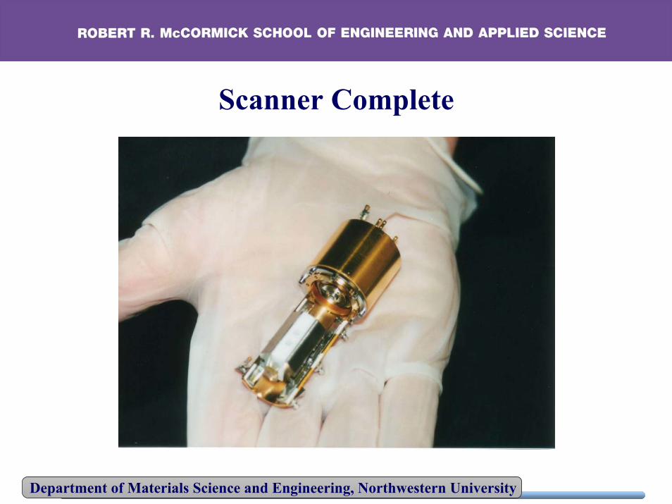
Scanner Complete

Department of Materials Science and Engineering, Northwestern University
Cryogenic Variable Temperature UHV STM

Department of Materials Science and Engineering, Northwestern University
Vibration Isolation

Department of Materials Science and Engineering, Northwestern University
Detail of Roof Plate
Department of Materials Science and Engineering, Northwestern University
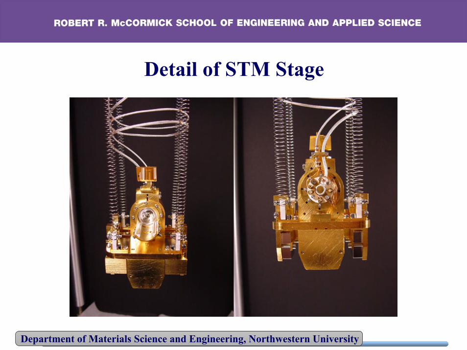
Detail of STM Stage
Department of Materials Science and Engineering, Northwestern University
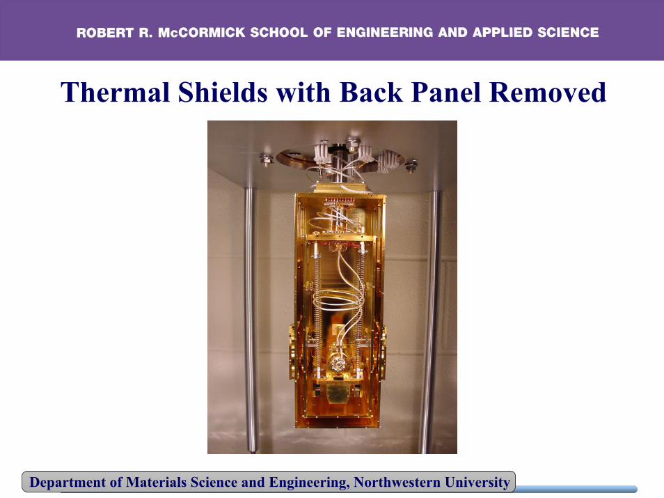
Thermal Shields with Back Panel Removed

Department of Materials Science and Engineering, Northwestern University
Stage Locking Screw for Cooldown and Cover

Department of Materials Science and Engineering, Northwestern University
Rear Door and Shutter Action

Department of Materials Science and Engineering, Northwestern University
Front Doors Open for STM Access

Department of Materials Science and Engineering, Northwestern University
Sample and Probe Mounted for Scanning

Department of Materials Science and Engineering, Northwestern University
Mirror Allows for Top-Down Viewof Tip-Sample Junction

Department of Materials Science and Engineering, Northwestern University
STM Suspended for Scanning

Department of Materials Science and Engineering, Northwestern University
UHV Chamber and Liquid Helium Dewar

Department of Materials Science and Engineering, Northwestern University
Scanning Tunneling Microscopy Nanofabrication
Many nanofabrication schemes have been developed with STM(spatial resolution down to the single atom level):
(1) Initially demonstrated by Eigler in 1989(“IBM” written with atoms at cryogenic temperatures)
(2) Room temperature atom removal from Si(111) by Avouris
(3) Field evaporation of gold
(4) Electron stimulated desorption of hydrogen from Si(100)

Department of Materials Science and Engineering, Northwestern University
Tunable Bond Formation with STM
G. Timp, Nanotechnology, Chapter 11

Department of Materials Science and Engineering, Northwestern University
Sliding Adatoms with STM
G. Timp, Nanotechnology, Chapter 11

Department of Materials Science and Engineering, Northwestern University
The First Atom Moved with STM
Xenon on platinum requires a defect to prevent tip-inducedmotion under normal scanning conditions
G. Timp, Nanotechnology, Chapter 11

Department of Materials Science and Engineering, Northwestern University
STM Manipulation of Xenon on Nickel
G. Timp, Nanotechnology, Chapter 11

Department of Materials Science and Engineering, Northwestern University
Nanograffiti
Don Eigler, IBM Alamden, http://www.almaden.ibm.com/vis/stm/atomo.html
Xenon atoms on Nickel (110) Fe atoms on Cu(111)
Kanji for atom:

Department of Materials Science and Engineering, Northwestern University
Don Eigler, IBM Alamden, http://www.almaden.ibm.com/vis/stm/atomo.html
Quantum Corrals
Fe atomson Cu(111)

Department of Materials Science and Engineering, Northwestern University
Don Eigler, IBM Alamden, http://www.almaden.ibm.com/vis/stm/atomo.html
Quantum Mirage (Kondo Resonance)
Co atomson Cu(111)
Topography:
dI/dV:

Department of Materials Science and Engineering, Northwestern University
Room Temperature Manipulation of Si(111)
C. Julian Chen, Introduction to Scanning Tunneling Microscopy

Department of Materials Science and Engineering, Northwestern University
Field Evaporation of Gold
C. Julian Chen, Introduction to Scanning Tunneling Microscopy

Department of Materials Science and Engineering, Northwestern University
550 Å × 550 Åfilled states
50 Å × 50 Åempty states
T = 650 KSi(100)-2×1:H
100 Å × 100 Åfilled states
T = 400 KSi(100)-3×1:H
Hydrogen PassivatedSi(100)
Department of Materials Science and Engineering, Northwestern University
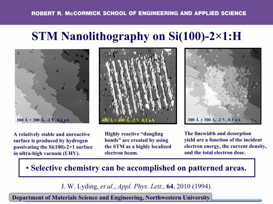
Highly reactive “danglingbonds” are created by usingthe STM as a highly localizedelectron beam.
400 Å × 400 Å, -2 V, 0.1 nA
• Selective chemistry can be accomplished on patterned areas.
The linewidth and desorptionyield are a function of the incidentelectron energy, the current density,and the total electron dose.
300 Å × 300 Å, -2 V, 0.1 nA
A relatively stable and unreactivesurface is produced by hydrogenpassivating the Si(100)-2×1 surfacein ultra-high vacuum (UHV).
300 Å × 300 Å, -2 V, 0.1 nA
STM Nanolithography on Si(100)-2×1:H
J. W. Lyding, et al., Appl. Phys. Lett., 64, 2010 (1994).

Department of Materials Science and Engineering, Northwestern University
Hydrogen Desorption Mechanisms

Department of Materials Science and Engineering, Northwestern University
Si
Si
Si
Si
Si
Si
Si
Si
Si
Si
Si
Si
Si
Si
Si
Si
2NBE
200 Å X 200 Å
After 2nd NBE Dose
Selective Molecular Adsorption of Norbornadiene on Silicon
G. C. Abeln, et al., J. Vac. Sci. Technol. B, 16, 3874 (1998).

Department of Materials Science and Engineering, Northwestern University
-3
-2
-1
0
1
2
3
0 0.02 0.04 0.06 0.08 0.1 0.12 0.14
Hydrogen Desorption Event
Z (Å)I (nA)
T (sec)
²z = 1.46 Å
Z (Å),I (nA)
ΔZ ~ 1.5 Å
170 Å X 170 Å, -2 V, 0.1 nA
Feedback Controlled Lithography
M. C. Hersam, et al., Nanotechnology, 11, 70 (2000).

Department of Materials Science and Engineering, Northwestern University
Styrene:R = phenyl
G.P Lopinski, et al., Nature, 406, 48 (2000).
Self-Directed Growth of Styrene Chainsfrom Individual Dangling Bonds

Department of Materials Science and Engineering, Northwestern University
Heteromolecular Nanostructuresvia Multi-Step FCL

Department of Materials Science and Engineering, Northwestern University
(c)
10-12
10-11
10-10
10-9
Loga
rithm
ic tu
nnel
ing
curr
ent (
A)
-4 -2 0 2 4Sample bias voltage (V)
-2
-1
0
1
2
Tunneling current (nA)
n-type
(d)
10-12
10-11
10-10
10-9
Loga
rithm
ic tu
nnel
ing
curr
ent (
A)
-4 -2 0 2 4Sample bias voltage (V)
-2
-1
0
1
2
Tunneling current (nA)
p-type
10 nm
(a) n-type
10 nm
(b) p-type
N. P. Guisinger, et al.,Nanotechology, 15, S452 (2004).
Degenerately Doped Si(100) Surfaces

Department of Materials Science and Engineering, Northwestern University
TEMPO on the Si(100)-2×1 Surface
B 3 nm
1 nm
C
A TEMPO NO
HCSi
TEMPO:(2,2,6,6-tetramethyl-1-piperidinyloxy)
DFT Optimized Geometry (Hyper Chem Release 7)
Individual TEMPO molecules are probed with the STM
N. P. Guisinger, et al., Nano Lett., 4, 55 (2004).

Department of Materials Science and Engineering, Northwestern University
I-V Curve for TEMPO on n+-Si(100)
-0.50
-0.25
0.00
0.25
0.50
Cur
rent
(nA
)-5.0 -2.5 0.0 2.5 5.0
Voltage (V)
TEMPO on n+-Si(100)
NDR
Shoulder
-3.0
-1.5
0.0
1.5
3.0
Cur
rent
(nA
)
-5.0 -2.5 0.0 2.5 5.0Voltage (V)
Clean n+-Si(100)
• NDR events are only observed at negative sample bias. • Shoulder is only observed at positive sample bias.• NDR bias values depend sensitively on tip-sample spacing• NDR is observed in both bias sweep directions
N. P. Guisinger, et al., Nano Lett., 4, 55 (2004).

Department of Materials Science and Engineering, Northwestern University
TEMPO on p+-Si(100)
-3.0
-1.5
0.0
1.5
3.0
Cur
rent
(nA
)
-5.0 -2.5 0.0 2.5 5.0Voltage (V)
NDR
Shoulder
Equilibrium NDRShoulder• Qualitatively similar behavior to TEMPO on n+-Si(100) except
opposite polarity.• Orbital energy shift may be due to charge transfer with the
substrate.
I-V Curve for TEMPO on p+-Si(100)N. P. Guisinger, et al., Nano Lett., 4, 55 (2004).

Department of Materials Science and Engineering, Northwestern University
STM Spectroscopy:CuPc and Au
Nanoelectrodeson NiAl(110)
G. V. Nazin, et al.,Science, 302, 77 (2003).
Department of Materials Science and Engineering, Northwestern University
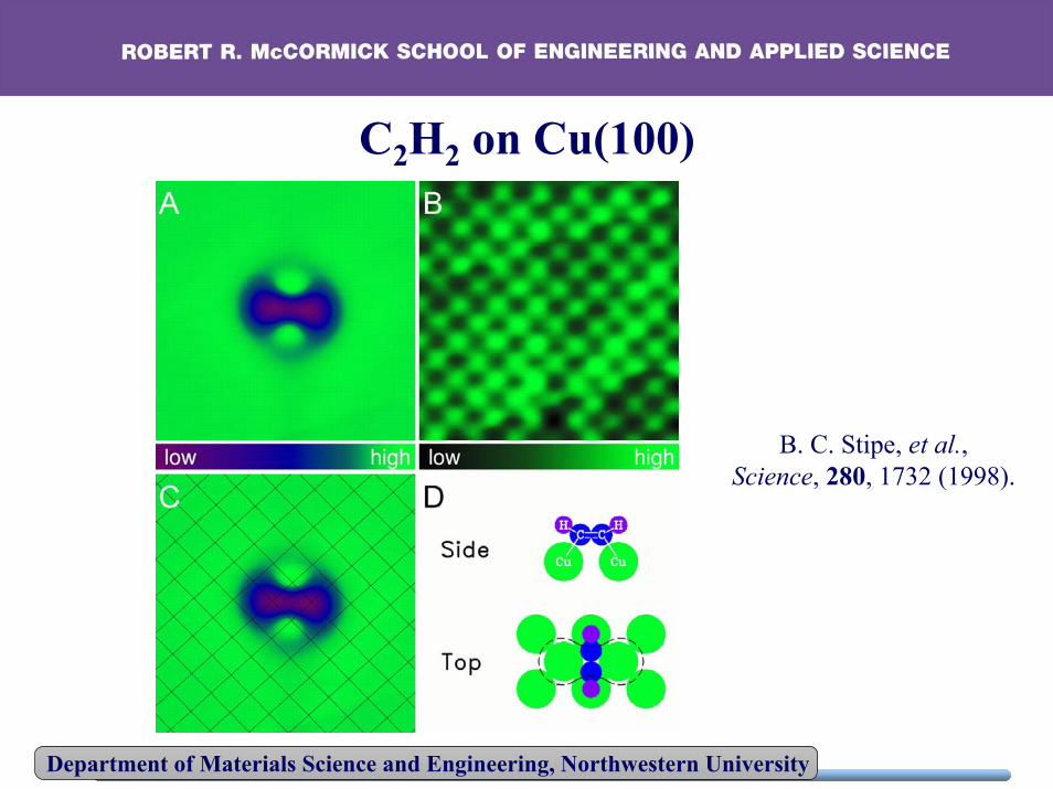
C2H2 on Cu(100)
B. C. Stipe, et al.,Science, 280, 1732 (1998).

Department of Materials Science and Engineering, Northwestern University
Inelastic Electron Tunneling Spectroscopy
B. C. Stipe, et al.,Science, 280, 1732 (1998).

Department of Materials Science and Engineering, Northwestern University
Spatial Maps of d2I/dV2
B. C. Stipe, et al., Science, 280, 1732 (1998).
Topo d2I/dV2
@ 358 mV
d2I/dV2
@ 311 mVd2I/dV2
@ 266 mV
C2H2 C2D2

Department of Materials Science and Engineering, Northwestern University
Contact Mode AFM Potentiometry
Biascircuit
Nanowire (50 Ω)
I
AFM Tip
Rl = 1-100 MΩ Picoammeter
Rc = 5 kΩ
Experimental setup:Requirements of AFM tip:
• Conductive tip with small Rc (kΩ range).• Low Rc must be sustained after extensive
scanning in contact mode.
Resolution requirements:
To analyze nanowire failure,
• Spatial resolution < 10 nm• Voltage sensitivity < 100 µV
Conductive diamond coated Si tipsprovide Rc = 5 kΩ with low wear ata repulsive force of 0.54 µN.

Department of Materials Science and Engineering, Northwestern University
Noncontact vs. Contact AFM PotentiometryNoncontact mode:
Image size = (1000 nm)2
0 V
0 V
-2 V
Contact mode:
Image size = (500 nm)2
-50 mV
-15 mV
Contact mode:
Image size = (500 nm)2
-90 mV
-120 mVp-pf = 6.8 mHz
• Noncontact mode AFM potentiometry possesses ~50 mV potentialsensitivity and ~50 nm spatial resolution.
• Contact mode AFM potentiometry possesses ~1 µV potential sensitivity,~5 nm spatial resolution, and ~0.01 ms time response.

Department of Materials Science and Engineering, Northwestern University
AFM Potentiometry of Nanowire Failure
B
Onset offailure
0.8V 1V C
Failurepoint
0.9V 1.8V
(Breakdown current density = 3.75×10¹² A/m2).
Contact mode AFM potentiometry images: Wire width = 60 nm
0.8V 1VA
Evolution of nanowire failure:
M. C. Hersam, et al., Appl. Phys. Lett., 72, 915 (1998).

Department of Materials Science and Engineering, Northwestern University
Atomic Force Electroluminescence Microscopy
L. S. C. Pingree, et al., Appl. Phys. Lett., 85, 344 (2004).

Department of Materials Science and Engineering, Northwestern University
AFEM on Micron Scale OLED Pixels
L. S. C. Pingree, et al., Appl. Phys. Lett., 85, 344 (2004).
• Spatial and temporal variations in current flow and electroluminescence can be directly probed.