1. Product profile
1.1 General description
Common-mode ElectroMagnetic Interference (EMI) filters with integrated ElectroStatic Discharge (ESD) protection for one, two and three differential channels. The devices are designed to provide low insertion loss for differential high-speed signals on each channel while unwanted common-mode signals are attenuated.
Each differential channel incorporates two signal lines that are coupled by integrated coils. Diodes provide protection to downstream components from ESD voltages up to ±15 kV on each signal line.
1.2 Features and benefits
One, two and three differential channels common-mode EMI filters with integrated ESD protection
ESD protection up to ±15 kV contact discharge according to IEC 61000-4-2
Superior common-mode suppression over a wide frequency range
Superior RF performance compared to other integrated filters or discrete filters with external ESD protection
Extremely high symmetry between line pairs
Industry-standard Wafer Level Chip Scale Packages: WLCSP5, 10 and 15 for smaller footprint
1.3 Applications
Smartphone, cellular and cordless phone
Tablet PC and Mobile Internet Device (MID)
USB 3.1, USB 2.0, HDMI 2.0, HDMI 1.4
MIPI M-PHY and D-PHY as used in Camera Serial Interface (CSI) and Display Serial Interface (DSI)
General-purpose EMI and Radio-Frequency Interference (RFI) filter and downstream ESD protection
PCMFxUSB30 seriesCommon-mode EMI filter for differential channels with integrated ESD protectionRev. 1 — 01 April 2016 Product data sheet
Table 1. Product overview
Type number Number of channels Package Name
PCMF1USB30 1 WLCSP5
PCMF2USB30 2 WLCSP10
PCMF3USB30 3 WLCSP15
Nexperia PCMFxUSB30 seriesCommon-mode EMI filter for differential channels with ESD protection
2. Pinning information
Table 2. Pinning
Pin Symbol Description Simplified outline Graphic symbol
PCMF1USB30 (WLCSP5_2-1-2)
A1 CH1_IN+ channel 1+, external
WLCSP5_2-1-2
A2 CH1_IN channel 1, external
B1 GND_CH1 ground channel 1
C1 CH1_OUT+ channel 1+, internal
C2 CH1_OUT channel 1, internal
PCMF2USB30 (WLCSP10_4-2-4)
A1 CH1_IN+ channel 1+, external
WLCSP10_4-2-4
A2 CH1_IN channel 1, external
A3 CH2_IN+ channel 2+, external
A4 CH2_IN channel 2, external
B1 GND_CH1 ground channel 1
B2 GND_CH2 ground channel 2
C1 CH1_OUT+ channel 1+, internal
C2 CH1_OUT channel 1, internal
C3 CH2_OUT+ channel 2+, internal
C4 CH2_OUT channel 2, internal
PCMF3USB30 (WLCSP15_6-3-6)
A1 CH1_IN+ channel 1+, external
WLCSP15_6-3-6
A2 CH1_IN channel 1, external
A3 CH2_IN+ channel 2+, external
A4 CH2_IN channel 2, external
A5 CH3_IN+ channel 3+, external
A6 CH3_IN channel 3, external
B1 GND_CH1 ground channel 1
B2 GND_CH2 ground channel 2
B3 GND_CH3 ground channel 3
C1 CH1_OUT+ channel 1+, internal
C2 CH1_OUT channel 1, internal
C3 CH2_OUT+ channel 2+, internal
C4 CH2_OUT channel 2, internal
C5 CH3_OUT+ channel 3+, internal
C6 CH3_OUT channel 3, internal
A B C
B1
1
2
Transparent top view
A1
A2
C1
C2
aaa-019784B1
A B C
B1
B2
1
2
3
4
Transparent top view
A1, 3
A2, 4
C1, 3
C2, 4
aaa-019785B1, B2 - no internal connection
B2
B3
B1
1
2
3
4
5
6
A B C
Transparent top view
A1, 3, 5
A2, 4, 6
C1, 3, 5
C2, 4, 6
aaa-019786B1, B2, B3 - no internal connection
© Nexperia B.V. 2017. All rights reservedPCMFXUSB30_SER All information provided in this document is subject to legal disclaimers.
Product data sheet Rev. 1 — 01 April 2016 2 of 23

Nexperia PCMFxUSB30 seriesCommon-mode EMI filter for differential channels with ESD protection
3. Ordering information
4. Marking
5. Limiting values
Table 3. Ordering information
Type number Package
Name Description Version
PCMF1USB30 WLCSP5 wafer level chip-size package; 5 bumps (2-1-2) PCMF1USB30
PCMF2USB30 WLCSP10 wafer level chip-size package; 10 bumps (4-2-4) PCMF2USB30
PCMF3USB30 WLCSP15 wafer level chip-size package; 15 bumps (6-3-6) PCMF3USB30
Table 4. Marking codes
Type number Marking code
PCMF1USB30 PF1S
PCMF2USB30 PF2S
PCMF3USB30 PF3S
Table 5. Limiting valuesIn accordance with the Absolute Maximum Rating System (IEC 60134).
Symbol Parameter Conditions Min Max Unit
VI input voltage 0.5 5 V
VESD electrostatic discharge voltage
IEC 61000-4-2, level 4; all input pins to ground
contact discharge 15 15 kV
air discharge 15 15 kV
IEC 61000-4-2, level 4; all output pins to ground
contact discharge 2 2 kV
air discharge 2 2 kV
IPPM rated peak pulse current
tp = 8/20 s 7 7 A
Tstg storage temperature 40 +125 C
Tamb ambient temperature 40 +85 C
© Nexperia B.V. 2017. All rights reservedPCMFXUSB30_SER All information provided in this document is subject to legal disclaimers.
Product data sheet Rev. 1 — 01 April 2016 3 of 23

Nexperia PCMFxUSB30 seriesCommon-mode EMI filter for differential channels with ESD protection
6. Characteristics
6.1 Channel characteristics
[1] This parameter is guaranteed by design.
[2] 100 ns Transmission Line Pulse (TLP); 50 W; pulser at 70 ns to 90 ns.
[3] According to IEC 61000-4-5 (8/20 ms).
6.2 Frequency characteristics
[1] Normalized to attenuation at 1 MHz.
Table 6. Channel characteristicsTamb = 25 C unless otherwise specified.
Symbol Parameter Conditions Min Typ Max Unit
Rs(ch) channel series resistance single line; input to output - 3 -
Cd diode capacitance f = 1 MHz; VI = 2.5 V [1] - 0.25 - pF
IRM reverse leakage current per line; VI = 5 V - - 100 nA
VBR breakdown voltage IR = 1 mA 6 9 - V
VF forward voltage IF = 10 mA - 0.8 - V
Rdyn dynamic resistance TLP [2]
positive transient - 0.14 -
negative transient - 0.14 -
surge [3]
positive transient - 0.22 -
negative transient - 0.22 -
Table 7. Frequency characteristics
Symbol Parameter Conditions Min Typ Max Unit
Common mode: S21cc
il insertion loss [1]
f = 800 MHz - 12 - dB
f = 2.6 GHz - 38 - dB
f = 5 GHz - 18 - dB
Differential mode: S21dd
il insertion loss f = 1 MHz [1] - 0.3 - dB
f3dB cut-off frequency [1] - 6 - GHz
© Nexperia B.V. 2017. All rights reservedPCMFXUSB30_SER All information provided in this document is subject to legal disclaimers.
Product data sheet Rev. 1 — 01 April 2016 4 of 23

Nexperia PCMFxUSB30 seriesCommon-mode EMI filter for differential channels with ESD protection
Fig 1. Differential-mode insertion loss; typical values Fig 2. Common-mode insertion loss; typical values
tr = 200 ps
Fig 3. Differential crosstalk; typical values Fig 4. Differential Time Domain Reflectometer (TDR) plot; typical values
aaa-019777
-4
-6
-2
0
Sdd21(dB)
-8
f (Hz)107 1010109108
S21dd pin 5 - 6
S21dd pin 1 - 2
f (Hz)107 1010109108
aaa-019778
-30
-20
-40
-10
0
Scc21(dB)
-50
S21cc pin 5 - 6
S21cc pin 1 - 2
aaa-021982
-40
-60
-20
0
Sdd21(db)
-80
f (Hz)107 10111010108 109
Mag S21dd A3 - A4 > C1 - C2
Mag S21dd A5 - A6 > C1 - C2
t (ns)40.4 41.241.040.6 40.8
aaa-019779
95
105
115
Zdif(Ω)
85
Z reference
Z DUT
© Nexperia B.V. 2017. All rights reservedPCMFXUSB30_SER All information provided in this document is subject to legal disclaimers.
Product data sheet Rev. 1 — 01 April 2016 5 of 23

Nexperia PCMFxUSB30 seriesCommon-mode EMI filter for differential channels with ESD protection
Data rate: 10 Gbit/s
Vertical scale: 173 mV/div
Horizontal scale: 20 ps/div
Fig 5. USB 3.1 eye diagram, test board with PCMF2USB30; typical values
Data rate: 10 Gbit/s
Vertical scale: 180 mV/div
Horizontal scale: 20 ps/div
Fig 6. USB 3.1 eye diagram, test board without device; typical values
© Nexperia B.V. 2017. All rights reservedPCMFXUSB30_SER All information provided in this document is subject to legal disclaimers.
Product data sheet Rev. 1 — 01 April 2016 6 of 23

Nexperia PCMFxUSB30 seriesCommon-mode EMI filter for differential channels with ESD protection
Data rate: 5 Gbit/s
Vertical scale: 169 mV/div
Horizontal scale: 40 ps/div
Fig 7. USB 3.1 eye diagram, test board with PCMF2USB30; typical values
Data rate: 5 Gbit/s
Vertical scale: 179 mV/div
Horizontal scale: 40 ps/div
Fig 8. USB 3.1 eye diagram, test board without device; typical values
© Nexperia B.V. 2017. All rights reservedPCMFXUSB30_SER All information provided in this document is subject to legal disclaimers.
Product data sheet Rev. 1 — 01 April 2016 7 of 23

Nexperia PCMFxUSB30 seriesCommon-mode EMI filter for differential channels with ESD protection
Test frequency: 148.5 MHz
Differential swing voltage: 861 mV
Horizontal scale: 34 ps/div
Fig 9. HDMI 2.0 eye diagram TP1, test board with PCMF2USB30; typical values
Test frequency: 148.5 MHz
Differential swing voltage: 917 mV
Horizontal scale: 34 ps/div
Fig 10. HDMI 2.0 eye diagram TP1, test board without device; typical values
© Nexperia B.V. 2017. All rights reservedPCMFXUSB30_SER All information provided in this document is subject to legal disclaimers.
Product data sheet Rev. 1 — 01 April 2016 8 of 23

Nexperia PCMFxUSB30 seriesCommon-mode EMI filter for differential channels with ESD protection
Test frequency: 148.5 MHz
Differential swing voltage: 849 mV
Horizontal scale: 34 ps/div
Remark: Measured at Test Point 2 (TP2) worst cable emulator, reference cable equalizer and worst case positive skew.
Fig 11. HDMI 2.0 eye diagram TP2, test board with PCMF2USB30; typical values
Test frequency: 148.5 MHz
Differential swing voltage: 909 mV
Horizontal scale: 34 ps/div
Remark: Measured at Test Point 2 (TP2) worst cable emulator, reference cable equalizer and worst case positive skew.
Fig 12. HDMI 2.0 eye diagram TP2, test board without device; typical values
© Nexperia B.V. 2017. All rights reservedPCMFXUSB30_SER All information provided in this document is subject to legal disclaimers.
Product data sheet Rev. 1 — 01 April 2016 9 of 23

Nexperia PCMFxUSB30 seriesCommon-mode EMI filter for differential channels with ESD protection
Vertical scale: 145 mV/div
Horizontal scale: 15.6 ns/div
Fig 13. MIPI M-PHY PWM-TX transmitter eye opening at 140 mV, test board with PCMF2USB30; typical values
Vertical scale: 146 mV/div
Horizontal scale: 15.6 ns/div
Fig 14. MIPI M-PHY PWM-TX transmitter eye opening at 140 mV, test board without device; typical values
© Nexperia B.V. 2017. All rights reservedPCMFXUSB30_SER All information provided in this document is subject to legal disclaimers.
Product data sheet Rev. 1 — 01 April 2016 10 of 23

Nexperia PCMFxUSB30 seriesCommon-mode EMI filter for differential channels with ESD protection
Vertical scale: 145 mV/div
Horizontal scale: 15.6 ns/div
Fig 15. MIPI M-PHY PWM-TX transmitter eye opening at 140 mV, test board with PCMF2USB30; typical values
Vertical scale: 146 mV/div
Horizontal scale: 15.6 ns/div
Fig 16. MIPI M-PHY PWM-TX transmitter eye opening at 140 mV, test board without device; typical values
© Nexperia B.V. 2017. All rights reservedPCMFXUSB30_SER All information provided in this document is subject to legal disclaimers.
Product data sheet Rev. 1 — 01 April 2016 11 of 23

Nexperia PCMFxUSB30 seriesCommon-mode EMI filter for differential channels with ESD protection
The device uses an advanced clamping structure showing a negative dynamic resistance. This snapback behavior strongly reduces the clamping voltage to the system behind the ESD protection during an ESD event. Do not connect unlimited DC current sources to the data lines to avoid keeping the ESD protection device in snapback state after exceeding breakdown voltage (due to an ESD pulse for instance).
Transmission Line Pulse (TLP) = 100 ns;
tr = 1 ns
Transmission Line Pulse (TLP) = 100 ns;
tr = 1 ns
Fig 17. Dynamic resistance with positive clamping; typical values
Fig 18. Dynamic resistance with negative clamping; typical values
Very-Fast Transmission Line Pulse (VF-TLP) = 5 ns;tr = 600 ps
Very-Fast Transmission Line Pulse (VF-TLP) = 5 ns;tr = 600 ps
Fig 19. Dynamic resistance with positive clamping; typical values
Fig 20. Dynamic resistance with negative clamping; typical values
VCL (V)0 252010 155
aaa-019781
10
15
5
20
25
I(A)
0
VCL (V)-25 0-5-15 -10-20
aaa-019782
-15
-10
-20
-5
0
I(A)
-25
VCL (V)0 252010 155
aaa-021984
10
15
5
20
25
I(A)
0
VCL (V)-25 0-5-15 -10-20
aaa-021983
-15
-10
-20
-5
0
I(A)
-25
© Nexperia B.V. 2017. All rights reservedPCMFXUSB30_SER All information provided in this document is subject to legal disclaimers.
Product data sheet Rev. 1 — 01 April 2016 12 of 23

Nexperia PCMFxUSB30 seriesCommon-mode EMI filter for differential channels with ESD protection
According to IEC 61000-4-5 (8/20 s) According to IEC 61000-4-5 (8/20 s)
Fig 21. Dynamic resistance with positive clamping; typical values
Fig 22. Dynamic resistance with negative clamping; typical values
VCL (V)0 1084 62
aaa-022150
4
6
2
8
10
I(A)
0
VCL (V)-10 0-2-6 -4-8
aaa-022151
-6
-4
-8
-2
0
I(A)
-10
© Nexperia B.V. 2017. All rights reservedPCMFXUSB30_SER All information provided in this document is subject to legal disclaimers.
Product data sheet Rev. 1 — 01 April 2016 13 of 23

Nexperia PCMFxUSB30 seriesCommon-mode EMI filter for differential channels with ESD protection
7. Application information
The device is designed to provide high-level ESD protection and common-mode filtering for differential high-speed data line pairs such as:
• USB 3.1
• HDMI 2.0
• Transition-Minimized Differential Signaling (TMDS)
• DisplayPort
• external Serial Advanced Technology Attachment (eSATA)
• Low Voltage Differential Signaling (LVDS)
When designing the PCB, give careful consideration to impedance matching and signal coupling. Do not connect the protected signal lines to unlimited current sources like, for example, a battery.
Since the SuperSpeed TX/RX lines are separated by GND or VBUS from the Hi-Speed lines, PCMF1USB30 makes it easy to achieve same signal lengths, straight routing, and optimal positioning for ESD protection directly at the connector.
Fig 23. Application diagram: protecting and filtering the differential data lines of a USB Type-C connector evaluation dongle with PCMF1USB30
© Nexperia B.V. 2017. All rights reservedPCMFXUSB30_SER All information provided in this document is subject to legal disclaimers.
Product data sheet Rev. 1 — 01 April 2016 14 of 23

Nexperia PCMFxUSB30 seriesCommon-mode EMI filter for differential channels with ESD protection
8. Package outline
Fig 24. Package outline WLCSP5
ReferencesOutlineversion
Europeanprojection Issue date
IEC JEDEC JEITA
PCMF1USB30
pcmf1usb30_po
Unit
mmmaxnommin
0.60 0.38 0.82 1.22
A
Dimensions (mm are the original dimensions)
WLCSP5: wafer level chip-size package; 5 bumps (2-1-2) PCMF1USB30
A1 b
0.31
D E e e1 e2
0.800.57 0.37 0.77 1.17 0.40 0.400.260.54 0.36 0.72 1.120.21
0 1 mm
scale
detail X
A
A1
X
A
B
C
E
D
21
e2
e1
e
b
1/2 e
B1
bump A1index area
bump A1index area
16-03-22
© Nexperia B.V. 2017. All rights reservedPCMFXUSB30_SER All information provided in this document is subject to legal disclaimers.
Product data sheet Rev. 1 — 01 April 2016 15 of 23

Nexperia PCMFxUSB30 seriesCommon-mode EMI filter for differential channels with ESD protection
Fig 25. Package outline WLCSP10
ReferencesOutlineversion
Europeanprojection Issue date
IEC JEDEC JEITA
PCMF2USB30
pcmf2usb30_po
Unit
mmmaxnommin
0.60 0.38 1.62
1.52
1.22
A
Dimensions (mm are the original dimensions)
WLCSP10: wafer level chip-size package; 10 bumps (4-2-4) PCMF2USB30
A1 b
0.31
D E e e1 e2
0.800.57 0.37 1.57 1.17 0.40 0.40
e3
0.800.260.54 0.36 1.120.21
0 1 mm
scale
16-03-22
detail X
A
A1
X
A
B
C
E
D
e2
e1B2B1
bump A1index area
bump A1index area
e b
43e3
21
1/2 e
© Nexperia B.V. 2017. All rights reservedPCMFXUSB30_SER All information provided in this document is subject to legal disclaimers.
Product data sheet Rev. 1 — 01 April 2016 16 of 23
Nexperia PCMFxUSB30 seriesCommon-mode EMI filter for differential channels with ESD protection
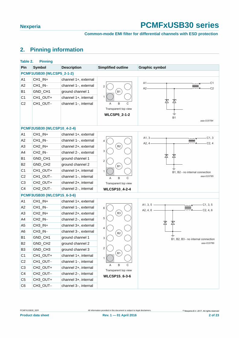
Fig 26. Package outline WLCSP15
ReferencesOutlineversion
Europeanprojection Issue date
IEC JEDEC JEITA
PCMF3USB30
pcmf3usb30_po
Unit
mmmaxnommin
0.60 0.38 2.42 1.220.80
A
Dimensions (mm are the original dimensions)
WLCSP15: wafer level chip-size package; 15 bumps (6-3-6) PCMF3USB30
A1 b
0.31
D E e e1 e2
0.80
e3
0.57 0.37 2.37 1.17 0.40 0.400.260.54 0.36 2.32 1.120.21
0 1 mm
scale
detail X
A
A1
D
E
bump A1index area
bump A1index area X
e2
e
e1
e3
b
1 2 43 65
A
B
C
1/2 e
B1 B2 B3
16-03-22
© Nexperia B.V. 2017. All rights reservedPCMFXUSB30_SER All information provided in this document is subject to legal disclaimers.
Product data sheet Rev. 1 — 01 April 2016 17 of 23
Nexperia PCMFxUSB30 seriesCommon-mode EMI filter for differential channels with ESD protection
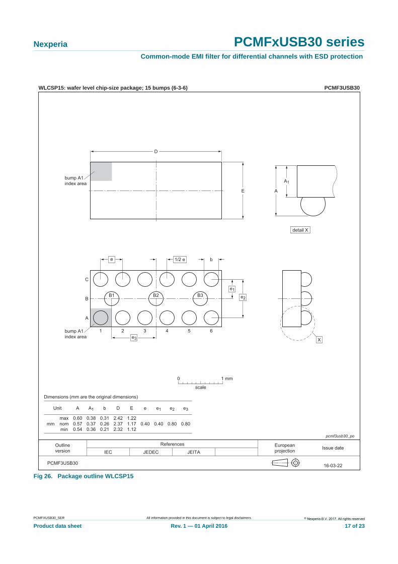
9. Soldering
Fig 27. Soldering footprint WLCSP5 (PCMF1USB30)
WLCSP5: Solder footprint and stencil aperture PCMF1USB30
pcmf1usb30_fr
solder resist opening (SR)
occupied area
solder land plus solder paste
solder paste deposit (SP)
solder land (SL)
Dimensions in mm
SRP
0.25 0.325
Hx
1.00
SL
0.25
SP
0.4016-03-22
Hy
1.40
SL = SP
SR
detail X
seedetail X
P
P
Hx
Hy
recommend stencil thickness: 0.1 mm
© Nexperia B.V. 2017. All rights reservedPCMFXUSB30_SER All information provided in this document is subject to legal disclaimers.
Product data sheet Rev. 1 — 01 April 2016 18 of 23
Nexperia PCMFxUSB30 seriesCommon-mode EMI filter for differential channels with ESD protection
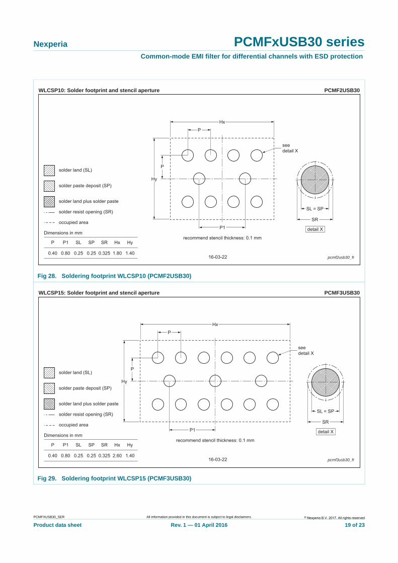
Fig 28. Soldering footprint WLCSP10 (PCMF2USB30)
Fig 29. Soldering footprint WLCSP15 (PCMF3USB30)
WLCSP10: Solder footprint and stencil aperture PCMF2USB30
pcmf2usb30_fr
solder resist opening (SR)
occupied area
solder land plus solder paste
solder paste deposit (SP)
solder land (SL)
Dimensions in mm
P1 SRP
0.80 0.25 0.325
Hx
1.80
SL
0.25
SP
0.4016-03-22
Hy
1.40
SL = SP
SR
detail X
seedetail X
P
P
P1
Hx
Hy
recommend stencil thickness: 0.1 mm
WLCSP15: Solder footprint and stencil aperture PCMF3USB30
pcmf3usb30_fr
solder resist opening (SR)
occupied area
solder land plus solder paste
solder paste deposit (SP)
solder land (SL)
Dimensions in mm
P1 SRP
0.80 0.25 0.325
Hx
2.60
SL
0.25
SP
0.4016-03-22
recommend stencil thickness: 0.1 mmHy
1.40
SL = SP
SR
detail X
seedetail X
P
P
P1
Hx
Hy
© Nexperia B.V. 2017. All rights reservedPCMFXUSB30_SER All information provided in this document is subject to legal disclaimers.
Product data sheet Rev. 1 — 01 April 2016 19 of 23

Nexperia PCMFxUSB30 seriesCommon-mode EMI filter for differential channels with ESD protection
10. Revision history
Table 8. Revision history
Document ID Release date Data sheet status Change notice Supersedes
PCMFXUSB30_SER v.1 20160401 Product data sheet - -
© Nexperia B.V. 2017. All rights reservedPCMFXUSB30_SER All information provided in this document is subject to legal disclaimers.
Product data sheet Rev. 1 — 01 April 2016 20 of 23

Nexperia PCMFxUSB30 seriesCommon-mode EMI filter for differential channels with ESD protection
11. Legal information
11.1 Data sheet status
[1] Please consult the most recently issued document before initiating or completing a design.
[2] The term ‘short data sheet’ is explained in section “Definitions”.
[3] The product status of device(s) described in this document may have changed since this document was published and may differ in case of multiple devices. The latest product status information is available on the Internet at URL http://www.nexperia.com.
11.2 Definitions
Draft — The document is a draft version only. The content is still under internal review and subject to formal approval, which may result in modifications or additions. Nexperia does not give any representations or warranties as to the accuracy or completeness of information included herein and shall have no liability for the consequences of use of such information.
Short data sheet — A short data sheet is an extract from a full data sheet with the same product type number(s) and title. A short data sheet is intended for quick reference only and should not be relied upon to contain detailed and full information. For detailed and full information see the relevant full data sheet, which is available on request via the local Nexperia sales office. In case of any inconsistency or conflict with the short data sheet, the full data sheet shall prevail.
Product specification — The information and data provided in a Product data sheet shall define the specification of the product as agreed between Nexperia and its customer, unless Nexperia and customer have explicitly agreed otherwise in writing. In no event however, shall an agreement be valid in which the Nexperia product is deemed to offer functions and qualities beyond those described in the Product data sheet.
11.3 Disclaimers
Limited warranty and liability — Information in this document is believed to be accurate and reliable. However, Nexperia does not give any representations or warranties, expressed or implied, as to the accuracy or completeness of such information and shall have no liability for the consequences of use of such information. Nexperia takes no responsibility for the content in this document if provided by an information source outside of Nexperia.
In no event shall Nexperia be liable for any indirect, incidental, punitive, special or consequential damages (including - without limitation - lost profits, lost savings, business interruption, costs related to the removal or replacement of any products or rework charges) whether or not such damages are based on tort (including negligence), warranty, breach of contract or any other legal theory.
Notwithstanding any damages that customer might incur for any reason whatsoever, Nexperia’s aggregate and cumulative liability towards customer for the products described herein shall be limited in accordance with the Terms and conditions of commercial sale of Nexperia.
Right to make changes — Nexperia reserves the right to make changes to information published in this document, including without limitation specifications and product descriptions, at any time and without notice. This document supersedes and replaces all information supplied prior to the publication hereof.
Suitability for use — Nexperia products are not designed, authorized or warranted to be suitable for use in life support, life-critical or safety-critical systems or equipment, nor in applications where failure or malfunction of a Nexperia product can reasonably be expected to result in personal injury, death or severe property or environmental damage. Nexperia and its suppliers accept no liability for inclusion and/or use of Nexperia products in such equipment or applications and therefore such inclusion and/or use is at the customer’s own risk.
Applications — Applications that are described herein for any of these products are for illustrative purposes only. Nexperia makes no representation or warranty that such applications will be suitable for the specified use without further testing or modification.
Customers are responsible for the design and operation of their applications and products using Nexperia products, and Nexperia accepts no liability for any assistance with applications or customer product design. It is customer’s sole responsibility to determine whether the Nexperia product is suitable and fit for the customer’s applications and products planned, as well as for the planned application and use of customer’s third party customer(s). Customers should provide appropriate design and operating safeguards to minimize the risks associated with their applications and products.
Nexperia does not accept any liability related to any default, damage, costs or problem which is based on any weakness or default in the customer’s applications or products, or the application or use by customer’s third party customer(s). Customer is responsible for doing all necessary testing for the customer’s applications and products using Nexperia products in order to avoid a default of the applications and the products or of the application or use by customer’s third party customer(s). Nexperia does not accept any liability in this respect.
Limiting values — Stress above one or more limiting values (as defined in the Absolute Maximum Ratings System of IEC 60134) will cause permanent damage to the device. Limiting values are stress ratings only and (proper) operation of the device at these or any other conditions above those given in the Recommended operating conditions section (if present) or the Characteristics sections of this document is not warranted. Constant or repeated exposure to limiting values will permanently and irreversibly affect the quality and reliability of the device.
Terms and conditions of commercial sale — Nexperia products are sold subject to the general terms and conditions of commercial sale, as published at http://www.nexperia.com/profile/terms, unless otherwise agreed in a valid written individual agreement. In case an individual agreement is concluded only the terms and conditions of the respective agreement shall apply. Nexperia hereby expressly objects to applying the customer’s general terms and conditions with regard to the purchase of Nexperia products by customer.
No offer to sell or license — Nothing in this document may be interpreted or construed as an offer to sell products that is open for acceptance or the grant, conveyance or implication of any license under any copyrights, patents or other industrial or intellectual property rights.
Document status[1][2] Product status[3] Definition
Objective [short] data sheet Development This document contains data from the objective specification for product development.
Preliminary [short] data sheet Qualification This document contains data from the preliminary specification.
Product [short] data sheet Production This document contains the product specification.
© Nexperia B.V. 2017. All rights reservedPCMFXUSB30_SER All information provided in this document is subject to legal disclaimers.
Product data sheet Rev. 1 — 01 April 2016 21 of 23

Nexperia PCMFxUSB30 seriesCommon-mode EMI filter for differential channels with ESD protection
Export control — This document as well as the item(s) described herein may be subject to export control regulations. Export might require a prior authorization from competent authorities.
Quick reference data — The Quick reference data is an extract of the product data given in the Limiting values and Characteristics sections of this document, and as such is not complete, exhaustive or legally binding.
Non-automotive qualified products — Unless this data sheet expressly states that this specific Nexperia product is automotive qualified, the product is not suitable for automotive use. It is neither qualified nor tested in accordance with automotive testing or application requirements. Nexperia accepts no liability for inclusion and/or use of non-automotive qualified products in automotive equipment or applications.
In the event that customer uses the product for design-in and use in automotive applications to automotive specifications and standards, customer (a) shall use the product without Nexperia’s warranty of the
product for such automotive applications, use and specifications, and (b) whenever customer uses the product for automotive applications beyond Nexperia’s specifications such use shall be solely at customer’s own risk, and (c) customer fully indemnifies Nexperia for any liability, damages or failed product claims resulting from customer design and use of the product for automotive applications beyond Nexperia’s standard warranty and Nexperia’s product specifications.
Translations — A non-English (translated) version of a document is for reference only. The English version shall prevail in case of any discrepancy between the translated and English versions.
11.4 TrademarksNotice: All referenced brands, product names, service names and trademarks are the property of their respective owners.
12. Contact information
For more information, please visit: http://www.nexperia.com
For sales office addresses, please send an email to: [email protected]
© Nexperia B.V. 2017. All rights reservedPCMFXUSB30_SER All information provided in this document is subject to legal disclaimers.
Product data sheet Rev. 1 — 01 April 2016 22 of 23

Nexperia PCMFxUSB30 seriesCommon-mode EMI filter for differential channels with ESD protection
13. Contents
1 Product profile . . . . . . . . . . . . . . . . . . . . . . . . . . 11.1 General description . . . . . . . . . . . . . . . . . . . . . 11.2 Features and benefits . . . . . . . . . . . . . . . . . . . . 11.3 Applications . . . . . . . . . . . . . . . . . . . . . . . . . . . 1
2 Pinning information. . . . . . . . . . . . . . . . . . . . . . 2
3 Ordering information. . . . . . . . . . . . . . . . . . . . . 3
4 Marking . . . . . . . . . . . . . . . . . . . . . . . . . . . . . . . . 3
5 Limiting values. . . . . . . . . . . . . . . . . . . . . . . . . . 3
6 Characteristics. . . . . . . . . . . . . . . . . . . . . . . . . . 46.1 Channel characteristics . . . . . . . . . . . . . . . . . . 46.2 Frequency characteristics. . . . . . . . . . . . . . . . . 4
7 Application information. . . . . . . . . . . . . . . . . . 14
8 Package outline . . . . . . . . . . . . . . . . . . . . . . . . 15
9 Soldering . . . . . . . . . . . . . . . . . . . . . . . . . . . . . 18
10 Revision history. . . . . . . . . . . . . . . . . . . . . . . . 20
11 Legal information. . . . . . . . . . . . . . . . . . . . . . . 2111.1 Data sheet status . . . . . . . . . . . . . . . . . . . . . . 2111.2 Definitions. . . . . . . . . . . . . . . . . . . . . . . . . . . . 2111.3 Disclaimers . . . . . . . . . . . . . . . . . . . . . . . . . . . 2111.4 Trademarks. . . . . . . . . . . . . . . . . . . . . . . . . . . 22
12 Contact information. . . . . . . . . . . . . . . . . . . . . 22
13 Contents . . . . . . . . . . . . . . . . . . . . . . . . . . . . . . 23
© Nexperia B.V. 2017. All rights reservedFor more information, please visit: http://www.nexperia.comFor sales office addresses, please send an email to: [email protected] Date of release: 01 April 2016
Recommended