Embed Size (px)
Citation preview

Rose-Hulman Institute of TechnologyRose-Hulman ScholarGraduate Theses - Electrical and ComputerEngineering Graduate Theses
5-2018
Differential Launch Structures and CommonMode Filters for Planar Transmission LinesZachary Thomas Bergstedt
Follow this and additional works at: https://scholar.rose-hulman.edu/electrical_grad_theses
Part of the Electrical and Electronics Commons
This Thesis is brought to you for free and open access by the Graduate Theses at Rose-Hulman Scholar. It has been accepted for inclusion in GraduateTheses - Electrical and Computer Engineering by an authorized administrator of Rose-Hulman Scholar. For more information, please [email protected].
Recommended CitationBergstedt, Zachary Thomas, "Differential Launch Structures and Common Mode Filters for Planar Transmission Lines" (2018).Graduate Theses - Electrical and Computer Engineering. 9.https://scholar.rose-hulman.edu/electrical_grad_theses/9

Differential Launch Structures and Common Mode Filters for Planar Transmission Lines
A Thesis
Submitted to the Faculty
of
Rose-Hulman Institute of Technology
by
Zachary Thomas Bergstedt
In Partial Fulfillment of the Requirements for the Degree
of
Master of Science in Electrical Engineering
May 2018
© 2018 Zachary Thomas Bergstedt


ABSTRACT
Bergstedt, Zachary Thomas
M.S.E.E.
Rose-Hulman Institute of Technology
May 2018
Differential Launch Structures and Common Mode Filters for Planar Transmission Lines
Thesis Advisor: Dr. Edward Wheeler
Increases in signal speeds and decreases in dimensions pose increasing threats to signal
integrity (SI) and electromagnetic compatibility (EMC) in differential interconnects due to the
enhanced risk of common mode (CM) conversion. This thesis examines CM filtering solutions
for multiple transmission topologies that mitigate CM noise, reducing the threat to SI and EMC.
These topologies include microstrip and stripline, which are the most commonly used
transmission line architecture in printed circuit boards (PCB), and broadside coupled coplanar
waveguides (BC-CPW). Stripline and BC-CPW transmission lines have lower dispersion and
attenuation than the commonly used microstrip but have added complexity in introducing the
signal to the transmission line in a PCB environment. Differential signal launches are introduced
that maintain differential transmission from DC to 20 GHz with less than -8 dB of common
mode conversion and better than -3.5 dB.
Keywords:

i
TABLE OF CONTENTS
LIST OF FIGURES ................................................................................................................................... iii
LIST OF TABLES ...................................................................................................................................... v
LIST OF ABBREVIATIONS ................................................................................................................... vi
LIST OF SYMBOLS ................................................................................................................................ vii
GLOSSARY.............................................................................................................................................. viii
1. INTRODUCTION ............................................................................................................................... 1
2. BACKGROUND ................................................................................................................................. 3
2.1. Even and Odd Mode Transmission Line Characteristics .............................................................. 3
2.2. Mixed-mode Transmission Line Characteristics .......................................................................... 6
2.3. Differential Transmission ............................................................................................................. 7
2.4. Scattering Parameters .................................................................................................................... 9
3. LITERATURE REVIEW................................................................................................................. 13
3.1. Mode-Selective Transmission Lines and Their Relationship To Common Mode Filtering ....... 13
3.2. Common Mode Filtering Structures ........................................................................................... 15
4. A MODEL FOR COMMON MODE FILTERING ....................................................................... 18
4.1. Quarter Wavelength Resonator ................................................................................................... 18
4.2. Common Mode Filtering in Microstrip Environments ............................................................... 18
4.3. Common Mode Filtering in Stripline Environments .................................................................. 20
4.4. Common Mode Filtering in Broadside Coupled CPW ............................................................... 22
4.5. Differential Launch Structure for a Stripline Environment ........................................................ 24
4.6. Differential Launch Structure for Broadside Coupled Coplanar Waveguide ............................. 27
5. FILTER AND LAUNCH STRUCTURE DESIGN AND VALIDATION ................................... 30
5.1. Microstrip Filtering Structures .................................................................................................... 33
5.2. Stripline Launch Structures and Filters ....................................................................................... 34
5.3. Broadside Coupled Coplanar Waveguide Launch Structure and Filters ..................................... 38
6. PERFORMANCE AND DISCUSSION OF LAUNCH STRUCTURES AND FILTERS .......... 46
6.1. Stripline and Broadside Coupled Coplanar Waveguide Launch Structures ............................... 47
6.2. Microstrip Filter Performance ..................................................................................................... 53
6.3. Stripline Filter Performance ........................................................................................................ 57
6.4. Broadside Coupled Coplanar Waveguide Filter Performance .................................................... 58

ii
7. LIMITATIONS ................................................................................................................................. 64
8. FUTURE WORK .............................................................................................................................. 66
9. CONCLUSION ................................................................................................................................. 69
REFERENCES .......................................................................................................................................... 70
APPENDICES ........................................................................................................................................... 71
Appendix A: Single-Ended to Mixed-Mode S-Parameter Conversions ................................................. 71
Appendix B: Test Board Models and Pictures ........................................................................................ 72
Appendix C: S-Parameter Results for All Filter Structures .................................................................... 74

iii
LIST OF FIGURES
Figure 2.1: Three-Wire Transmission Line Network ............................................................5
Figure 2.2: Odd-Mode Excitation of a Three Wire Transmission Line Network ..................6
Figure 2.3: Asymmetry in Coupled Transmission Lines .......................................................8
Figure 2.4: Four-port Coupled Transmission Lines ...............................................................9
Figure 3.1: Mode-Selective Transmission Line Architecture ................................................14
Figure 3.2: Differential Mode-Selective Transmission Line Architecture ............................15
Figure 3.3: Typical Common Mode Filtering Structures.......................................................16
Figure 3.4: Flux Structures in a Defected Ground Plane Filter .............................................17
Figure 4.2: Microstrip Bowtie Filter ......................................................................................19
Figure 4.3: Stripline Cross Section ........................................................................................21
Figure 4.4: Stripline Bowtie Filter .........................................................................................22
Figure 4.5: Broadside Coupled Coplanar Waveguide Bowtie Filter .....................................23
Figure 4.6: Stripline Transition ..............................................................................................25
Figure 4.7: Broadside Coupled Coplanar Waveguide Transition ..........................................28
Figure 5.1: Mixed-Mode S-Parameter Measurement Setup ..................................................32
Figure 5.2: Bowtie Filter Structures Implemented in Microstrip ..........................................33
Figure 5.3: Stripline Launch Structure Dimensions ..............................................................35
Figure 5.4: Bowtie Filter Structures Implemented in Stripline ..............................................37
Figure 5.5: BC-CPW Launch Structure Dimensions .............................................................38
Figure 5.6: Bowtie Filter Structures Implemented in BC-CPW ............................................43
Figure 6.1: BC-CPW Launch Structure S-Parameter Results ...............................................47
Figure 6.2: BC-CPW Time Domain Reflectometer Measurement Results ...........................49
Figure 6.3: Stripline Launch Structure S-Parameter Results .................................................51
Figure 6.4: Microstrip Filtering Structure S-Parameter Results ............................................54
Figure 6.5: Stripline Filtering Structure S-Parameter Results ...............................................58
Figure 6.6: BC-CPW 11 GHz Filtering Structure S-Parameter Results ................................59

iv
Figure 6.7: BC-CPW Cascaded Filtering Structures S-Parameter Results ............................60
Figure 6.8: BC-CPW Asymmetric Filtering Structure S-Parameter Results .........................60
Figure 6.9: BC-CPW RF Probe Launched Filter S-Parameter Results .................................61
Figure B.1: Test Board Overview ..........................................................................................72
Figure C.1: Microstrip 3 Cascaded Symmetric Filters S-Parameter Results .........................74
Figure C.2: Microstrip 2 Cascaded Symmetric Filters S-Parameter Results .........................74
Figure C.3: Microstrip Single Asymmetric Filter S-Parameter Results ................................75
Figure C.4: Stripline Single Symmetric 5 GHz Filter S-Parameter Results ..........................76
Figure C.5: Stripline Single Symmetric 8 GHz Filter S-Parameter Results ..........................76
Figure C.6: Stripline Single Symmetric 16 GHz Filter S-Parameter Results ........................77
Figure C.7: Stripline 3 Cascaded Symmetric Filters S-Parameter Results ............................77
Figure C.8: BC-CPW Single Symmetric 8 GHz Filter S-Parameter Results ........................78
Figure C.9: BC-CPW Single Symmetric 11 GHz Filter S-Parameter Results ......................78
Figure C.10: BC-CPW Single Symmetric 16 GHz Filter S-Parameter Results ....................79
Figure C.11: BC-CPW 3 Cascaded Symmetric Filters S-Parameter Results ........................79
Figure C.12: BC-CPW 2 Cascaded Symmetric Filters S-Parameter Results ........................80
Figure C.13: BC-CPW Single Asymmetric Filter S-Parameter Results ................................80
Figure C.14: BC-CPW RF Probe 3 Cascaded Symmetric Filters S-Parameter Results ........81
Figure C.15: BC-CPW RF Probe 2 Cascaded Symmetric Filters S-Parameter Results ........81
Figure C.16: BC-CPW RF Probe Single Asymmetric Filters S-Parameter Results ..............82

v
LIST OF TABLES
Table 5.1: Microstrip Filter Dimensions ................................................................................34
Table 5.2: Stripline Launch Dimensions ...............................................................................36
Table 5.3: Stripline Filter Dimensions ...................................................................................37
Table 5.4: BC-CPW Launch Dimensions ..............................................................................42
Table 5.5: BC-CPW Filter Dimensions .................................................................................45
Table B.1: Test Board Overview ...........................................................................................73

vi
LIST OF ABBREVIATIONS
BC-CPW Broadside Coupled Coplanar Waveguide
CM Common Mode
CPW Coplanar Waveguide
DM Differential Mode
EMC Electromagnetic Compatibility
MSTL Mode Selective Transmission Line
PCB Printed Circuit Board
SI Signal Integrity

vii
LIST OF SYMBOLS
𝜆 Wavelength
𝑍𝑐 Characteristic Impedance
𝐶 Capacitance
𝑉 Voltage
𝐼 Current
𝑎 Incoming power wave
𝑏 Outgoing power wave
𝑆𝑖𝑗 Scattering parameter from port j to port i
𝜖 Relative permittivity
𝑣𝑝 Electromagnetic propagation velocity
𝑐 The propagation velocity of light in free space
Ω Ohms

viii
GLOSSARY
Wave Number - a parameter of how much the phase of a progresses in a unit of distance
Common Mode - a mode of energy when two excitations have the same amplitude and direction
Differential Mode - a mode of energy when two excitations have the same amplitude and
opposite directions
Signal Integrity - the input signal reaches the output port
Electromagnetic Compatibility - the lack of interference from one region of a circuit with
another region of a circuit, whether the same circuit or a different one
Characteristic Impedance - the ratio relating the voltage and current in a transmission line

ix

1
1. INTRODUCTION
Differential mode signaling is often used in high speed interconnects to mitigate noise and
crosstalk. This becomes more difficult with continuing increases in signal speeds and shrinking
dimensions, which represent twin challenges to the limits of existing interconnect technology.
The presence of common mode conversion, when differential mode energy is converted to
common mode energy, represents a significant threat to the electromagnetic compatibility (EMC)
and signal integrity (SI) environment of printed circuit boards (PCBs), a challenge which grows
more serious as frequencies continue to increase and the wavelengths shrink. Common mode
(CM) filtering solutions exist to mitigate the presence of CM noise but may be unsuitable due to
their lack of effectiveness, their frequency limitations, or their added complexity and cost.
A critical enabling technology and an area overlooked in research investigations is signal
launch. A practical signal launch, offering high-performance over a wide range of frequencies
is critical if the CM filtering structures are ever going to be used in applications and in
commercial products. Whatever the topology of the differential communication link and its
associated CM filtering structure is, effective signal launches must be brought to one side of the
PCB since modern integrated circuit use a ball-grid array to make electrical contact to the host
PCB. Regardless of the CM filtering solution’s effectiveness, their utility will be limited without
signal launches providing access to the structures on a single side of a PCB. The signal launch is
therefore crucial, and its performance must be such that it remains effective over a broad range
of frequencies, a difficult task at microwave and mm-wave frequencies.
In work reported here, signal launches are designed for coplanar waveguide (CPW) based
structures, which rely on broadside coupling to form differential communication links, and also
for stripline based structures with edge coupling. Both CPW and stripline show effective

2
transmission through mm-range wavelengths. This can be contrasted with microstrip based
structures which display significant loss (largely due to radiation) at higher frequencies.

3
2. BACKGROUND
In order to analyze the filters and launch structures, an understanding of even and odd mode
analysis, common and differential mode transmission, and single-ended and mixed-mode
scattering parameters (S-parameters) is needed. In particular, mixed-mode S-parameters and
their relationship to single-ended S-parameters are important to understand. Single-ended S-
parameters are what is measured and mixed-mode S-parameters are what is used to characterize
the differential transmission line network.
2.1. Even and Odd Mode Transmission Line Characteristics
Electromagnetic energy propagates as waves, in free space as “plane waves,” so-called since
their surfaces of constant phase form planes. These waves can be characterized by the intrinsic
impedance of the medium, 𝜂, and the wave number, 𝛽. The intrinsic impedance is the ratio of
magnitudes between the electric and magnetic fields, and the wavenumber is inversely related to
the wavelength and is the number of waves in 2 meters. In free space, the wave number is
related to wavelength by the following equation.
𝛽 =2𝜋
𝜆= 2𝜋𝑓√𝜇𝜖
(2.1)
and the intrinsic impedance is related to permittivity, 𝜖, and permeability, 𝜇, by the following
equation.
𝜂 = √𝜇
𝜖
(2.2)
These two parameters characterize the propagation of the wave. In transmission lines,
Maxwell’s equations can be simplified by allowing the use of transmission line equations which
are expressed in terms of voltages and currents. The voltage is obtained with a line integral of
the electric field from one conductor to another, and the current is obtained by finding the

4
circulation of the magnetic field about a conductor. In transmission lines, the waves can be
characterized similarly by the characteristic impedance, 𝑍𝑐, which includes the geometry and
electric and magnetic materials of the media in the transmission line. The characteristic
impedance can be expressed in terms of L and C, the transmission line’s per-unit-length (PUL)
inductance and capacitance.
𝑍𝑐 = √𝐿
𝐶
(2.3)
With the basis of a single transmission line, we can start to analyze two coupled
transmission lines. In most cases, these coupled lines consist of two transmission lines with a
single reference plane, though there may be multiple reference planes that are at the same
potential. As a circuit, this can be modeled as shown in Fig. 2.1(b) [1], where 𝐶11 represents the
capacitance between trace 1 and reference, 𝐶12 represents the capacitance between traces, and
𝐶22 represents the capacitance between trace 2 and ground. The inductance, 𝐿, is not affected as
strongly as capacitance, and will not be considered. Assuming the traces are identical, 𝐶11 =
𝐶22.
(a)

5
(b)
Fig. 2.1 - (a) Three-wire transmission line network and (b) the equivalent capacitance network
With this model, consider an even mode excitation, where the currents in the traces are
equal in amplitude and direction and consider an odd mode excitation, where the currents in the
traces are equal in amplitude but in opposite directions. Correspondingly, in the even mode,
𝑉1 = 𝑉2 and in the odd mode, 𝑉1 = −𝑉2. In the even mode, there will be no current through 𝐶12
which can be replaced by an open circuit. Because of this, the capacitance from either line in the
even mode, 𝐶𝑒, will just equal 𝐶11 or 𝐶22. The characteristic impedance will then be equal to
𝑍𝑐𝑒 = √𝐿
𝐶𝑒
(2.4)
In the odd mode excitation, the flux pattern will be odd symmetric about a plane in the
center between the two traces. In the circuit model, this can be treated as a ground plane
between the two capacitances as shown in Fig. 2.2(b) [1].
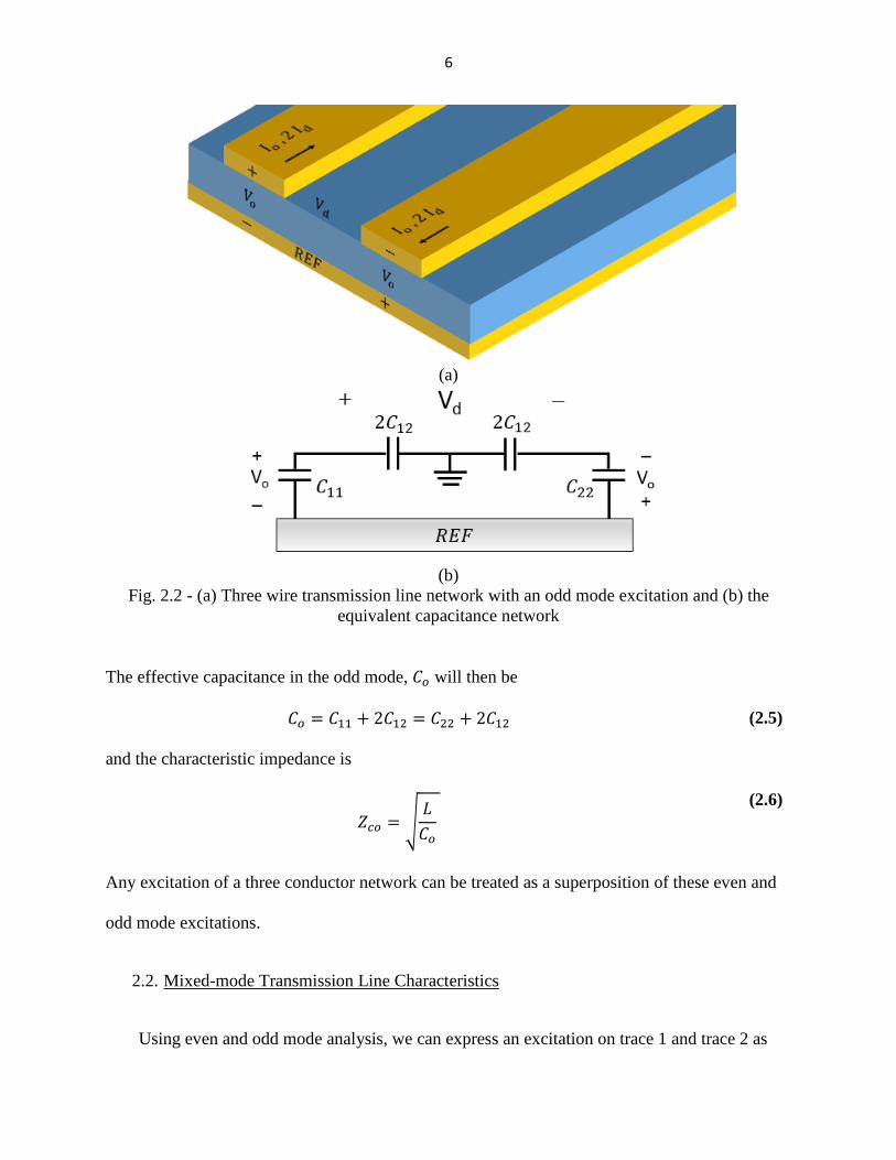
6
(a)
(b)
Fig. 2.2 - (a) Three wire transmission line network with an odd mode excitation and (b) the
equivalent capacitance network
The effective capacitance in the odd mode, 𝐶𝑜 will then be
𝐶𝑜 = 𝐶11 + 2𝐶12 = 𝐶22 + 2𝐶12 (2.5)
and the characteristic impedance is
𝑍𝑐𝑜 = √𝐿
𝐶𝑜
(2.6)
Any excitation of a three conductor network can be treated as a superposition of these even and
odd mode excitations.
2.2. Mixed-mode Transmission Line Characteristics
Using even and odd mode analysis, we can express an excitation on trace 1 and trace 2 as

7
𝑉1 =𝑉𝑒 + 𝑉𝑜
2
(2.7)
𝑉2 =𝑉𝑒 − 𝑉𝑜
2
(2.8)
respectively [2]. The average or common mode voltage will be
𝑉𝑐 =𝑉1 + 𝑉2
2
(2.9)
and the difference or differential mode voltage will be
𝑉𝑑 = 𝑉1 − 𝑉2 (2.10)
Similarly, the currents will be
𝐼𝑐 = 𝐼1 + 𝐼2 (2.11a)
𝐼𝑑 =𝐼1 − 𝐼2
2
(2.11b)
Using these definitions, the common and differential mode impedances will thus be
𝑍𝑐𝑐 =1
2
𝑉1 + 𝑉2
𝐼1 + 𝐼2=
1
2𝑍𝑐𝑒
(2.12a)
𝑍𝑐𝑑 = 2𝑉1 − 𝑉2
𝐼1 − 𝐼2= 2 𝑍𝑐𝑜
(2.12b)
2.3. Differential Transmission
Differential mode signaling has several advantages over single-ended signaling and is
commonly used in digital interconnects. In pure differential signaling, there will be no net
current through any cross section that surrounds both traces, so unwanted radiation and
subsequence electromagnetic interference (EMI) will be reduced. In the near-field, crosstalk is
reduced through reduced net electric and magnetic coupling. Additionally, any DC offset will be
canceled out and the effects of noise may be reduced due to the close proximity that results in a
correlation of the noise, which will also be canceled out.
8
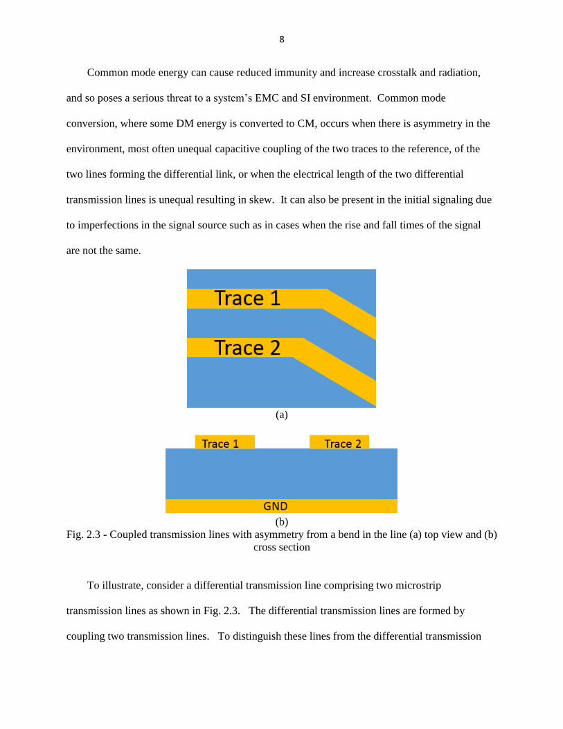
Common mode energy can cause reduced immunity and increase crosstalk and radiation,
and so poses a serious threat to a system’s EMC and SI environment. Common mode
conversion, where some DM energy is converted to CM, occurs when there is asymmetry in the
environment, most often unequal capacitive coupling of the two traces to the reference, of the
two lines forming the differential link, or when the electrical length of the two differential
transmission lines is unequal resulting in skew. It can also be present in the initial signaling due
to imperfections in the signal source such as in cases when the rise and fall times of the signal
are not the same.
(a)
(b)
Fig. 2.3 - Coupled transmission lines with asymmetry from a bend in the line (a) top view and (b)
cross section
To illustrate, consider a differential transmission line comprising two microstrip
transmission lines as shown in Fig. 2.3. The differential transmission lines are formed by
coupling two transmission lines. To distinguish these lines from the differential transmission

9
line they form, they are usually referred to as “single-ended” lines so that two coupled single-
ended lines form a differential transmission line. As seen in Fig. 2.3, a bend in the signal path
results in one line becoming longer than the other, introducing skew which could result in CM
conversion and its attendant negative effects.
2.4. Scattering Parameters
The microstrip-based differential transmission line shown above can be considered a four-
port (four single-ended ports, that is) network as illustrated in Fig. 2.4. The port parameters used
at microwave and mm-wave signals are described in terms of power waves, which are
proportional to the square root of the wave’s power. Power waves directed toward the ports are
denoted as a1, a2, …, aN referring the waves going into ports 1, 2, …, N. Similarly, power waves
leaving the ports are denoted as b1, b2, …, bN
Fig. 2.4 - Coupled TL network as a four-port device
Power waves are defined as
𝑎 =𝑉 + 𝑍𝑐𝐼
2√𝑍𝑐
=𝑉+
√𝑍𝑐
(2.13a)
𝑏 =𝑉 − 𝑍𝑐𝐼
2√𝑍𝑐
=𝑉−
√𝑍𝑐
(2.13b)

10
where a is the incident power wave, and b is the reflected or outgoing power wave. 𝑉+and 𝑉−
are the incident and outgoing voltage waves respectively [1]. Similarly to voltages, power waves
can likewise be defined for differential mode and common mode.
𝑎𝑑 =𝑉𝑑 + 𝑍𝑐𝑑𝐼𝑑
2√𝑍𝑐𝑑
(2.14a)
𝑎𝑐 =𝑉𝑐 + 𝑍𝑐𝑐𝐼𝑐
2√𝑍𝑐𝑐
(2.14b)
𝑏𝑑 =𝑉𝑑 − 𝑍𝑐𝑑𝐼𝑑
2√𝑍𝑐𝑑
(2.14c)
𝑏𝑐 =𝑉𝑐 − 𝑍𝑐𝑐𝐼𝑐
2√𝑍𝑐𝑐
(2.14d)
Using these power waves, it is more convenient to think of the two single-ended ports 1 and 3 as
forming a differential port 1 with both positive and negative-going differential mode and
common mode signals. Likewise one can consider single-ended ports 2 and 4 as forming
differential port 2 again with both positive and negative-going differential mode and common
mode signals. Assuming differential port 1 is comprised of single-ended ports 1 and 3 and
differential port 2 is comprised of single-ended ports 2 and 4, equations (2.9)-(2.12b) and
equations (2.14a-d) can be used to determine the relationship between these so-called mixed-
mode waves and single-ended power waves to be
𝑎𝑑1 =𝑎1 − 𝑎3
√2 (2.15a)
𝑎𝑐1 =𝑎1 + 𝑎3
√2
(2.15b)
𝑏𝑑1 =𝑏1 − 𝑏3
√2
(2.15c)

11
𝑏𝑐1 =𝑏1 + 𝑏3
√2
(2.15d)
At mixed-mode port 2, single-ended ports 2 and 4 are substituted for ports 1 and 3.
Scattering parameters are defined relative to the incident and reflected power waves. Let us
first consider the relationship between single-ended signals.
[𝑏1
⋮𝑏𝑁
] = [𝑆11 ⋯ 𝑆1𝑁
⋮ ⋱ ⋮𝑆𝑁1 ⋯ 𝑆𝑁𝑁
] [
𝑎1
⋮𝑎𝑁
] (2.16)
A specific element in the scattering matrix can be found as
𝑆𝑖𝑗 =𝑏𝑖
𝑎𝑗|
𝑎𝑘=0 𝑓𝑜𝑟 𝑘≠𝑗
(2.17)
where bi is the voltage reflected or directed in the outgoing direction at the ith port and ai is the
input voltage or the voltage going into the device at the jth port. For a four-port device, there
will be sixteen elements in the 4 x 4 scattering matrix. Using this relationship and the
relationships between single-ended and mixed-mode power waves from equations (2.15a-b),
mixed-mode scattering parameters can be derived from single-ended parameters.
In the common mode, 𝑎1 = 𝑎3 and in the differential mode, 𝑎1 = −𝑎3. Using the scattering
parameter relationship, the outgoing voltages at each port can be determined for common and
differential mode excitations.
[
𝑏1
𝑏2
𝑏3
𝑏4
] = [
𝑆11
𝑆21
𝑆31
𝑆41
𝑆13
𝑆23
𝑆33
𝑆43
] [𝑎1
𝑎3]
(2.18)
Mixed-mode scattering parameters are evaluated the same as single-ended scattering parameters
except the mode is included. For example, if the excitation is differential mode at mixed-mode

12
port 1 and the received signal is at mixed-mode port 2 in common mode, the scatting parameter
would be calculated as
𝑆𝑐𝑑21 =𝑏𝑐2
𝑎𝑑1|
𝑎𝑐𝑘=𝑎𝑑𝑘=0 𝑓𝑜𝑟 𝑘≠1
=𝑏2 + 𝑏4
𝑎1 − 𝑎3|
𝑎1=−𝑎3,𝑎𝑘=0 𝑓𝑜𝑟 𝑘≠1,3
(2.19)
The reflected power waves can then be related to the incident power waves using single-ended
scattering parameters using equation (2.18). Additionally, the incident power waves can be
related because of the mode. This yields
𝑆𝑐𝑑21 =(𝑆21 − 𝑆23)𝑎1 + (𝑆41 − 𝑆43)𝑎1
2𝑎1=
1
2(𝑆21 − 𝑆23 + 𝑆41 − 𝑆43)
(2.20)
This derivation can be repeated for each combination of input and output port and mode. The
most useful equations are given below. The rest are included in Appendix A.
Differential Mode Reflection: 𝑆𝑑𝑑11 = 1 2⁄ (𝑆11 − 𝑆13 − 𝑆31 + 𝑆33)
Differential Mode Reflection: 𝑆𝑑𝑑21 = 1 2⁄ (𝑆21 − 𝑆41 − 𝑆23 + 𝑆43)
Common Mode Conversion: 𝑆𝑐𝑑21 = 1 2⁄ (𝑆21 + 𝑆41 − 𝑆23 − 𝑆43)
Common Mode Transmission: 𝑆𝑐𝑐21 = 1 2⁄ (𝑆11 + 𝑆13 + 𝑆31 + 𝑆33)
(2.21a)
(2.21b)
(2.21c)
(2.21d)

13
3. LITERATURE REVIEW
Existing solutions for differential transmission may be inadequate for mm-wave
applications. Existing differential transmission line architectures have limited coupling between
the differential traces, limiting the benefits of using the differential transmission in the first place,
and loss and dispersion that becomes prohibitive in the mm-wave range. Existing common mode
filtering structures either require a shared, broadside coupled ground plane or are bandpass filters
that cannot accommodate wideband differential signals.
3.1. Mode-Selective Transmission Lines and Their Relationship To Common Mode Filtering
Limitations exist in stripline and microstrip transmission lines due to their dispersion and
attenuation at high frequencies. These architectures are adequate at low frequencies, and
solutions exist for propagation at high frequency. What is lacking is a transmission line
architecture able to accommodate wideband signals such as picosecond pulses which have
frequency components extending from DC to millimeter wave frequencies. A new architecture
was introduced in [3] called mode-selective transmission lines (MSTL) that has low dispersion
and attenuation both at low frequencies and at millimeter wave frequencies. In this architecture,
the top metal layer is a coplanar waveguide with vias connecting the coplanar reference with the
bottom reference layer as shown in Fig. 3.1. Careful design allows these vias to act as walls for a
surface integrated waveguide at high frequencies.

14
Fig. 3.1 - Mode-selective transmission line architecture
At low frequencies, the architecture has the flux pattern of a microstrip transmission line.
This is the TEM mode of operation where most of the flux is coupled from the microstrip line to
the ground plane. As the frequency increases, the flux becomes less confined to the microstrip
pattern and the TEM mode. Eventually, the TE10 mode dominates. In this mode, the electric
field spreads out to the via fence walls, approximating a rectangular waveguide.
This architecture is attractive for differential transmission and common mode filtering due
to its potential for symmetry that will not affect differential mode impedance but will alter
common mode impedance. Indeed, the earlier work by Ke Wu’s group [3] on these single-
ended structures was the original motivation for all the CPW-based structures shown here. If the
transmission line is mirrored across the ground plane, as depicted in Fig. 3.2(a), the middle
ground plane will isolate the two transmission lines. This topology will be referred to as
broadside coupled coplanar waveguide (BC-CPW).
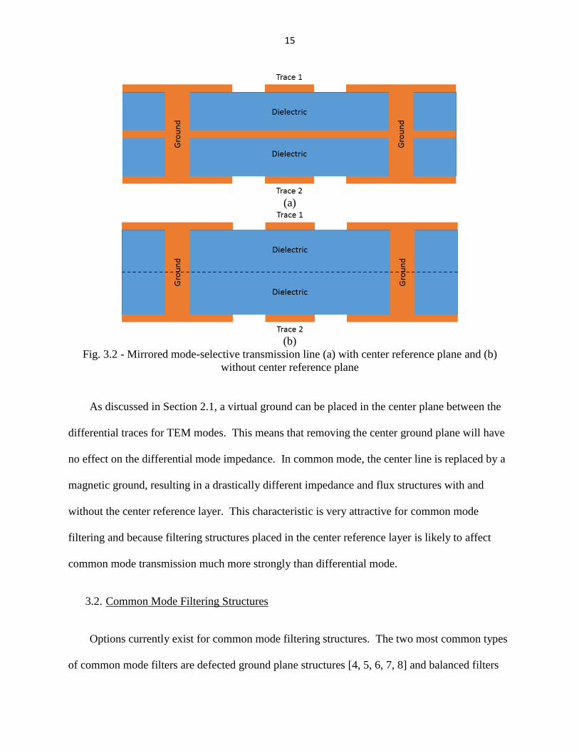
15
(a)
(b)
Fig. 3.2 - Mirrored mode-selective transmission line (a) with center reference plane and (b)
without center reference plane
As discussed in Section 2.1, a virtual ground can be placed in the center plane between the
differential traces for TEM modes. This means that removing the center ground plane will have
no effect on the differential mode impedance. In common mode, the center line is replaced by a
magnetic ground, resulting in a drastically different impedance and flux structures with and
without the center reference layer. This characteristic is very attractive for common mode
filtering and because filtering structures placed in the center reference layer is likely to affect
common mode transmission much more strongly than differential mode.
3.2. Common Mode Filtering Structures
Options currently exist for common mode filtering structures. The two most common types
of common mode filters are defected ground plane structures [4, 5, 6, 7, 8] and balanced filters

16
[4, 9, 10, 11]. Defected ground plane filters rely on net electric flux into the filter in common
mode and no net electric flux into the filter in differential mode, while balanced filters rely on the
symmetry of common mode versus the antisymmetry of differential mode.
(a)
(b)
Fig. 3.3 - Typical Common Mode filtering structures utilizes a (a) defected ground plane and a
(b) balanced bandpass filter
Defected ground plane filters consist of resonators embedded in the ground plane below the
differential transmission lines as in Fig. 3.3(a). In common mode, there is net flux into the
resonator, exciting it and hampering common mode transmission. In differential mode, there is
electric flux coupling into the resonator from one trace and electric flux coupling out of the
resonator to the other trace. The result is approximately zero net flux to the reference in the
differential mode, resulting in very little or no attenuation in differential mode transmission.

17
Fig. 3.4 - DM and CM flux patterns of a differential microstrip pair with defected ground plane
Balanced filters generally consist of a filter structure that is connected to both traces. The
balanced filter is often a single-ended filter mirrored about the center plane between the coupled
traces as in Fig. 3.3(b). With the symmetry of common mode, the combined filter acts as a
bandstop filter. With the antisymmetry of differential mode, the combined filter acts as a
bandpass filter where the differential pass band is the same as the common mode stop band.
Both filter types have their advantages. Defected ground plane structures are compact and
do not take up much space since they are in the ground plane which has to be there anyway.
Balanced filters double as bandpass filters and can have extremely high common mode rejection
ratios. However, both these filter types have drawbacks. They are nearly all designed for edge-
coupled microstrip transmission lines. They can be adapted to other transmission line topologies
like stripline but may have limited effectiveness and increased complexity. Additionally,
defected ground plane structures they are not easily adaptable to topologies like coplanar
waveguides where there is not a shared broadside coupled ground plane. Defected ground plane
filters are incompatible with the previously proposed BC-CPW topology for this reason and
because there will be no net electric flux through the center plane in common mode and net flux
in differential mode.

18
4. A MODEL FOR COMMON MODE FILTERING
The CM filtering structure examined here is useful primarily due to its simplicity and
adaptability. The quarter wavelength resonator has an uncomplicated design equation and can be
implemented in almost any differential topology. Practical use in stripline and BC-CPW
architectures require launch structures which are also considered below.
4.1. Quarter Wavelength Resonator
If a length of transmission line with a short at the end is placed in parallel as a stub with a
transmission line, it will act as a bandpass filter where the passband occurs when the length of
the stub is a quarter of the wavelength [1]. Conversely, if the short-circuited stub were placed in
series with transmission line, it would act as a notch filter, passing all frequencies except for
where the length is a quarter of the wavelength. This notch filter can be accomplished through
the use of a coupled line filter. Instead of the resonator directly touching the transmission line, it
is coupled to the transmission line. It can be shown through even and odd mode analysis that
this will result in a notch filter as if the resonator were in series with the transmission line [1].
Since the filter is excited by the electric flux of the transmission lines and the flux patterns of
common mode and differential mode signals are different, this filter can be implemented to only
affect the common mode transmission and not significantly impact the differential mode
transmission.
4.2. Common Mode Filtering in Microstrip Environments
Microstrip is one of the simplest architectures for transmission lines. It is simply a single
trace of copper above a ground plane. Since it is on the outer layer of the board, it requires no
transmission to link to a connector or component. Its simplicity and low-cost combine to make it

19
a common architecture. CM filtering can be accomplished by putting a bowtie filter in the
middle of the two coupled microstrip traces as in Fig. 4.2. This addition will have a small effect
on the differential impedance due to the non-ideality and finite size of the filter.
(a)
(b)
Fig. 4.2 - Bowtie filtering structure between microstrip traces (a) top view and (b) cross section
cut at the dotted line
The filter will attenuate most strongly when
𝐿1 + ℎ =𝜆
4
(4.2a)
𝐿2 + ℎ =𝜆
4
(4.2b)
where 𝜆 is the wavelength of a signal at a certain frequency. In order to design the filter, the
propagation velocity in the microstrip must be determined. This can be approximately
determined using equation (4.3a) which is based on a curve-fit approximation [1] and using
equation (4.3b)
𝜖𝑒 =𝜖𝑟 + 1
2+
𝜖𝑟 − 1
2
1
√1 + 12ℎ/𝑊
(4.3a)
𝑣𝑝 =𝑐
√𝜖𝑒
(4.3b)
GND

20
where 𝜖𝑟 is the relative permittivity of the substrate of the microstrip, ℎ and 𝑊 are dimensions of
the structure shown in Fig. 4.2, and 𝑐 is the speed of light in free space. With these results, the
filter can be designed for a specific frequency.
𝐿1 =𝑣𝑝
4𝑓1− ℎ
(4.4a)
𝐿2 =𝑣𝑝
4𝑓2− ℎ
(4.4b)
These equations are estimations, since the effective permittivity, 𝜖𝑒, in microstrip is not the same
for single-ended and differential and common modes. This is because in mixed-mode, a
different proportion of the flux is in the dielectric as compared with single-ended.
4.3. Common Mode Filtering in Stripline Environments
Stripline architecture consists of two metal reference layers with the signal trace in between
in the middle as in Fig. 4.3(a). The trace is surrounded by dielectric material. For differential
transmission, the single trace is replaced with two coupled traces as in Fig. 4.3(b). This trace
architecture is more convenient in multilayer boards and has less attenuation and radiation at
higher frequencies as compared to microstrip.
Filtering using bowtie structures is accomplished in stripline much the same as in
microstrip; a patch of metal with a via to reference. Just as with microstrip architecture, the
filters consist of two quarter-wavelength resonators that are excited by common mode but not
differential mode transmission. However, stripline traces couples very strongly with the
reference planes which is broadside to the trace as compared with the edge-coupling to the other
transmission line or to the filter. This results in limited filtering when no modification is made to
the reference plane since the filter is not strongly excited. Voids in the ground plane can
overcome this with limited effect to DM transmission.

21
(a)
(b)
Fig. 4.3 - Stripline cross section in (a) single-ended and (b) mixed-mode configurations
Just as in microstrip, the filters attenuate most strongly when the length of the filter
including the via distance to ground is a quarter of the wavelength. Unlike microstrip, the
effective permittivity is equal to the permittivity of the dielectric material. This somewhat
simplifies design because the predicted wavelength is not subject to inaccuracies of estimated
formulas.
Voiding the reference planes as in Fig. 4.4 will result in a decrease in the coupling to the
ground of the transmission lines. As the coupling to the reference planes decreases, a higher
proportion of the flux couples to the filtering structure. This results in deeper filtering
attenuation but may introduce a change in the differential impedance that hampers differential
transmission. The size of the voids was chosen to be the same length as the filter with the width
being as wide as the combined width of the transmission lines and the space between them.
These dimensions did not significantly impact differential transmission.

22
Fig. 4.4 - Differential stripline configuration with bowtie filter and voided ground planes
4.4. Common Mode Filtering in Broadside Coupled CPW
The Broadside Coupled CPW topology is especially good for common mode filtering due to
the potential for strong coupling between the differential traces and a filtering element placed
between the traces. The half wavelength bowtie structure can be implemented with great success
in this structure. Additional filtering structures have been proposed and have shown promise, but
they are not well characterized nor well understood.
In the case of a Broadside Coupled CPW, the bowtie structure is placed in a layer between
the top and bottom differential traces. Instead of a via, shorting stubs are included near the
center of the filter as in Fig. 4.5. The shorting pin connects from the filtering structure to a
reference in the same plane or to vias that connect the top and bottom coplanar references.
Another shorting pin is included on the opposite side of the filter to the other side of the
reference or to the other via fence.
As in other architectures, the filter consists of two quarter wavelength resonators. The
lengths 𝐿1 and 𝐿2 can be independently adjusted to achieve multiband filtering. Additionally,
the distance from the filter to the reference, ℎ, can be modified in this topology. This is in

23
contrast with stripline and microstrip where ℎ is determined by the thickness of the substrate.
Increasing this value allows for a shorter filter at a given frequency.
(a)
(b)
Fig. 4.5 - BC-CPW with a bowtie filter (a) perspective view and (b) top view of the filter layer
Because of the coupling strength of broadside coupling as compared with edge coupling, the
filtering in this topology is both deeper and broader than in the analogous microstrip or stripline
filter. The depth and breadth of filtering from a single filter in this topology suggests the use of
only a single filter. A single structure can then be used to achieve effective, broadband filtering
at multiple frequencies.

24
This topology is not yet well characterized, creating a slight difficulty in designing the filter.
The propagation velocity and effective permittivity, in particular, have not been described by any
design equations. At low frequencies, the single-ended effective permittivity is similar to but
slightly lower than the effective permittivity of a microstrip with the same trace width and
substrate thickness. At very high frequencies, the propagating mode is more confined within the
dielectric, resulting in an effective permittivity that is close to the permittivity of the material.
However, the propagating mode is not TEM at those frequencies; it is TE10. This mode has both
group and phase velocity which are not necessarily the same. The bowtie filter has only been
examined at frequencies dominated by the TEM mode.
Due to these considerations, only an estimate about the filtering center frequency can be
made. The bandwidth of the filter is large enough that an estimate suffices for most applications.
When an estimate is inadequate, simulation can be used to analyze and predict the filtering
frequency with a higher degree of confidence.
4.5. Differential Launch Structure for a Stripline Environment
The process for measuring a microstrip trace is rather simple. Connectors exist that can be
bolted or soldered onto the edge of a test board and have very good transmission characteristics
up to the frequencies at which microstrip begins radiating. In contrast, stripline requires a more
sophisticated launch structure in order to be measured with RF probes or coaxial connectors.
Specifically, a via transition is required from the top layer to the middle signal layer. Since the
signal trace is in the middle, a stub will be left below the trace (as in Fig. 4.6) due to back drilling
in the manufacturing process.

25
(a)
(b)
Fig. 4.6 - Stripline transition (a) top view and (b) cross-section cut at the dotted line showing via
and stub
The requirement for this transition poses several signal integrity and EMC challenges. First,
the via is a discontinuity that results in an impedance change and thus reflections. The stub has a
resonance associated that, when excited, will act as a filter, preventing transmission. The via
also has the potential to excite parallel plate waveguide modes, which, in addition to radiating
energy and harming transmission, can couple to the other differential trace and cause mode
conversion. If a parallel plate mode is excited, energy can be unintentionally transmitted and
interfere with circuitry in other areas of the printed circuit board.
The first challenge to be overcome is matching the transition to the launch. A coplanar
waveguide is used as a launch pad for the transmission line that runs from the input to the via
transition. The coplanar waveguide is designed to be 50 ohms. The transition should thus also
26
be designed to be 50 ohms. A pad must be included for the via. This pad will be slightly wider
than the coplanar waveguide trace, resulting in slightly increased capacitance. As a result, the
antipad must leave a gap to the reference that is slightly larger than the gap in the coplanar trace.
The via itself has capacitive coupling with the upper reference plane. The via is naturally
inductive, so the impedance will be approximately correct. Since the transition is relatively
small, the impedance must only approximately match the coplanar and stripline impedances.
The closer the match is, the higher in frequency the transmission will survive. Ultimately, a
physics-based design followed by simulation and modifications suffices for most applications.
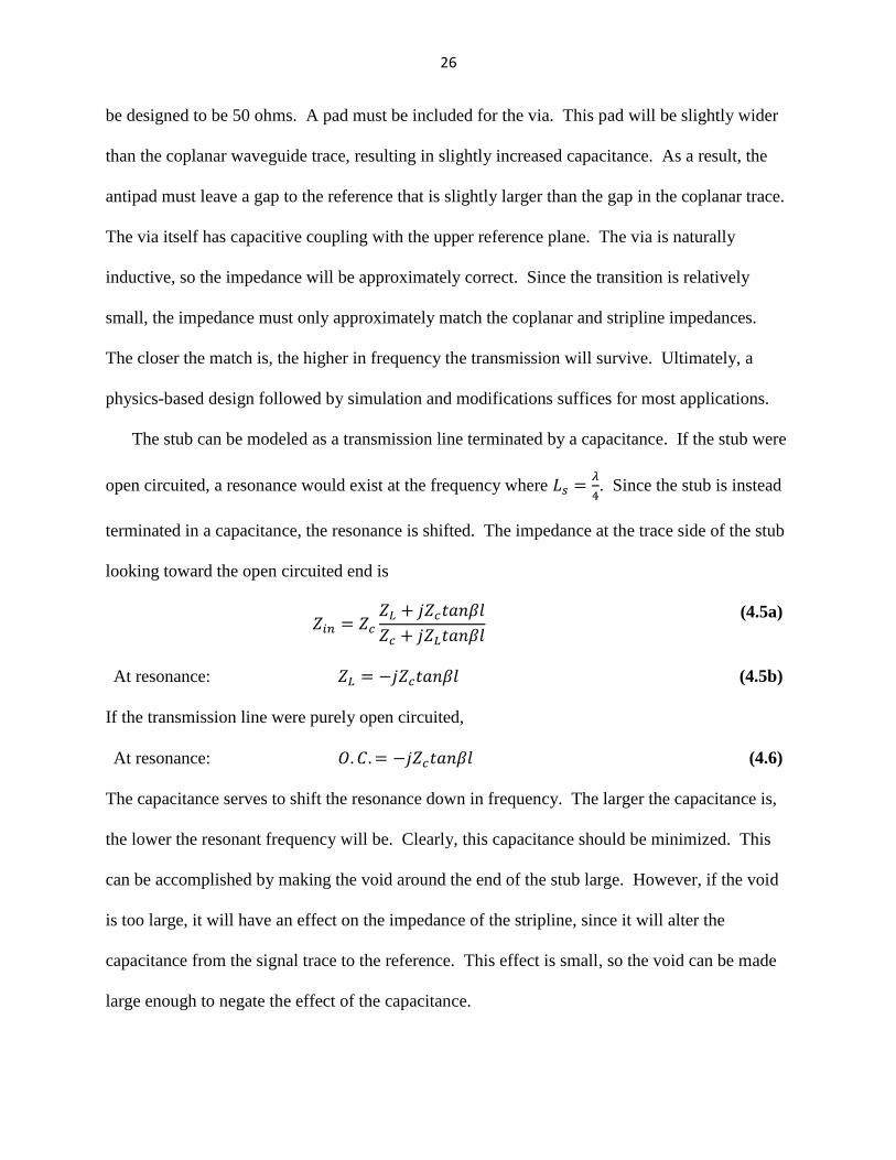
The stub can be modeled as a transmission line terminated by a capacitance. If the stub were
open circuited, a resonance would exist at the frequency where 𝐿𝑠 =𝜆
4. Since the stub is instead
terminated in a capacitance, the resonance is shifted. The impedance at the trace side of the stub
looking toward the open circuited end is
𝑍𝑖𝑛 = 𝑍𝑐
𝑍𝐿 + 𝑗𝑍𝑐𝑡𝑎𝑛𝛽𝑙
𝑍𝑐 + 𝑗𝑍𝐿𝑡𝑎𝑛𝛽𝑙
(4.5a)
At resonance: 𝑍𝐿 = −𝑗𝑍𝑐𝑡𝑎𝑛𝛽𝑙 (4.5b)
If the transmission line were purely open circuited,
At resonance: 𝑂. 𝐶. = −𝑗𝑍𝑐𝑡𝑎𝑛𝛽𝑙 (4.6)
The capacitance serves to shift the resonance down in frequency. The larger the capacitance is,
the lower the resonant frequency will be. Clearly, this capacitance should be minimized. This
can be accomplished by making the void around the end of the stub large. However, if the void
is too large, it will have an effect on the impedance of the stripline, since it will alter the
capacitance from the signal trace to the reference. This effect is small, so the void can be made
large enough to negate the effect of the capacitance.

27
Parallel plate waveguide mode excitation is avoided through the use of via fencing around
the launch structure. The via fencing serves to isolate the launch structure from other areas on
the PCB. Additionally, several vias are used to prevent coupling between the signal via
transitions.
4.6. Differential Launch Structure for Broadside Coupled Coplanar Waveguide
Like the stripline topology, the BC-CPW topology requires a launch that includes a via
transition in order to be measured. However, the BC-CPW has the added difficulty of requiring
an asymmetric launch to be probed from a single side. Asymmetry can result in common mode
conversion, and since the primary purpose of this topology is compact and strong common mode
filtering structures, common mode conversion must be firmly avoided. The launch structure
must be carefully designed than, so as to mitigate common mode conversion to the greatest
extent possible. This can be accomplished through a combination of impedance matching to
prevent asymmetric reflections and length compensation to mitigate skew.
A via transition is only needed in one of the two differential traces since only one of the
traces will be on the opposite side of the board from the input. On both traces, an MSTL runs
from the input. In the first trace, the MSTL continues into the device under test. In the second
trace, the MSTL goes to a via that goes through the board into another MSTL on the other side.
Two primary challenges exist in creating this launch structure. The via transition must be
matched to allow for good transmission on that trace and to avoid common mode conversion that
comes from mismatch between the two traces. Secondly, the difference in length that comes
from one trace having to run through the board and the other going directly to the device under
test must be accounted for and compensated.
28
(a)
(b)
Fig. 4.7 - BC-CPW launch transition (a) top view and (b) cross section cut at the dotted line
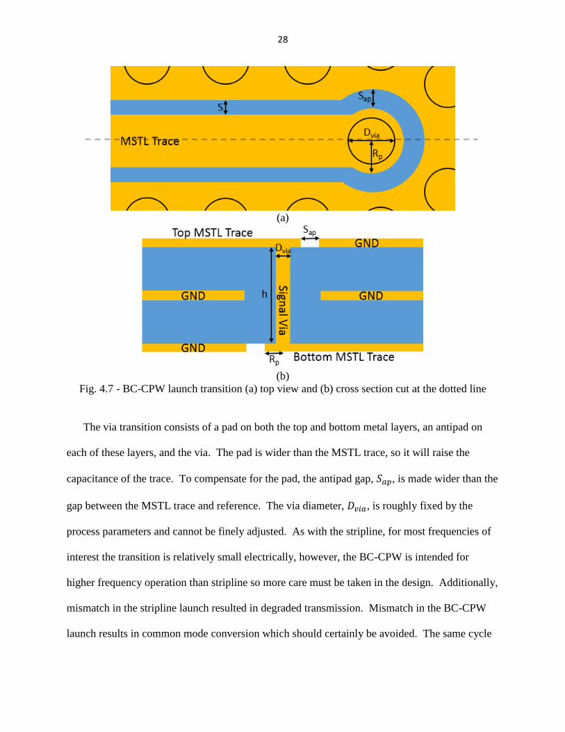
The via transition consists of a pad on both the top and bottom metal layers, an antipad on
each of these layers, and the via. The pad is wider than the MSTL trace, so it will raise the
capacitance of the trace. To compensate for the pad, the antipad gap, 𝑆𝑎𝑝, is made wider than the
gap between the MSTL trace and reference. The via diameter, 𝐷𝑣𝑖𝑎, is roughly fixed by the
process parameters and cannot be finely adjusted. As with the stripline, for most frequencies of
interest the transition is relatively small electrically, however, the BC-CPW is intended for
higher frequency operation than stripline so more care must be taken in the design. Additionally,
mismatch in the stripline launch resulted in degraded transmission. Mismatch in the BC-CPW
launch results in common mode conversion which should certainly be avoided. The same cycle

29
of a physics-based design followed by simulation and modification is taken in this structure, but
with more iterations to arrive at a better match.
The length is compensated for in the MSTL section of the launch. The trace without the via
transition is compensated with a length equal to the effective length of the via transition. The
first approximation of this length is just the height of the board without the outer metal layers, h.
Since the propagation velocity is not the same in the via transition as it in the MSTL, this will not
compensate exactly, but it will be close enough to serve as a start. After simulation,
modifications can be made to this length to compensate for the path length difference more
closely.

30
5. FILTER AND LAUNCH STRUCTURE DESIGN AND VALIDATION
The microstrip, stripline, and BC-CPW filter models and the stripline and BC-CPW launch
models are validated through computer simulation and measurement of fabricated structures. A
minimum of three filtering structures were simulated and fabricated for each topology of
microstrip, stripline, and BC-CPW. RF probe signal launches were simulated and fabricated for
both stripline and BC-CPW topologies. Additionally, a coaxial signal launch structure was
simulated, fabricated, and measured for the BC-CPW topology. These signal launches were used
in measuring the filtering structures in stripline and BC-CPW. The computer model and
fabricated version of the test board with the BC-CPW and stripline structures are shown in
Appendix B.
In order to have maximum confidence in the performance of the structures proposed, each is
both simulated and measured. The simulation results and the measurement are compared to
ensure the simulation reflects reality as closely as possible. The comparison of these results
serves to confirm the accuracy of the simulation. Once the simulations are matched to physical
measurement, additional simulations can be undertaken with an added degree of trust that these
simulation results might be replicated in a physical structure.
For the filtering structures, the primary characteristics examined are the frequencies of
operation and the attenuation. In comparison with the theoretical model, the center filtering
frequency should match within a certain margin of error that depends upon the topology and the
assumptions made. The impact of the filters on the differential mode transmission is predicted to
be negligible. Any major impact on the differential mode transmission caused by the filtering
structures represents a deviation from the theoretical predictions. When comparing simulated
and measured results, the band of the filter is primarily considered. This includes the frequencies

31
of the edges of the stopbands, the frequency of strongest filtering, and the overall attenuation.
Overall, the simulated and measured results should match closely, but some tolerance is given to
allow for manufacturing tolerances, dielectric mismatch, and other attributes not considered by
the simulation.
Both frequency and time domain analysis, simulation, and measurement are employed in this
investigation. We use mixed-mode scattering parameters (frequency-domain) and the impedance
as inferred through time domain reflectometry (TDR). Scattering parameters are discussed in
section 2.4, but in short, they characterize the effect the device measured has on signals at
different frequencies. The specific scattering parameters examined for validation are 𝑆𝑑𝑑21,
which is effectively the transmission from port 1 to port 2 in differential mode, 𝑆𝑐𝑐21, which is
effectively the transmission in common mode, and 𝑆𝑐𝑑21, which is effectively the conversion of
differential mode signal to common mode signal from port 1 to port 2. TDR is a time domain
based experimental probe which characterizes system characteristics based on the reflections
from an excitation in the form of a short pulse in the time domain (17 ps rise time). From these
reflections, the relative impedance can be mapped as a function of distance traveled. This TDR
measurement can be used to examine the characteristic impedance at various points in the
structure and check for mismatch, which is particularly useful in the revisions of the launch
structure for matching the transitions to the traces.
The measurement setup used for all devices is shown in Fig. 5.1. In the figure, the
measurements being taken are single-ended scattering parameters at port 1 and port 4 of the DUT
with the other ports terminated in matched loads. From equations 2.21(a-d), the single-ended
scattering parameters 𝑆11, 𝑆13, 𝑆31, 𝑆33, 𝑆21, 𝑆41, 𝑆23, and 𝑆43 must be taken. In real passive
devices, the scattering parameter matrix is symmetric, so only 𝑆31 or 𝑆13 must be taken since

32
they are equal. To obtain these single-ended scattering parameters, five configurations are
needed. These configurations will be denoted as follows: the DUT port to which VNA port 1 is
connected-the DUT port to which VNA port 2 is connected. Any DUT port not connected to the
VNA is terminated in a matched load. For example, the configuration in Fig. 5.1 is denoted 1-4.
To obtain the eight necessary single-ended scattering parameters, the following configurations
are needed: 1-2, 1-3, 1-4, 3-2, 3-4. Once the single-ended scattering parameters are obtained,
they are converted to mixed-mode scattering parameters using equations 2.21(a-d).
Fig. 5.1 - Setup used to measure mixed-mode scattering parameters
33
5.1. Microstrip Filtering Structures
(a)
(b)
(c)
(d)
(e)
Fig. 5.2 - (a-c) Top view of all three filtering structures for microstrip lines, (d) the fabricated
structures and (e) the cross section

34
Table 5.1
Structure
Dimensions (mm) Material Properties
W 1.88 εr = 3.0
S 1.88 εe = 2.41
Wf 1.00
T 0.035
Material:
Rogers 4730
h 0.77
d 0.8
Predicted Filter
Frequency (GHz)
(a)
L1 8.6 5.15
L2 5.0 8.37
L3 1.9 18.08
(b)
L1 8.6 5.15
L2 5.5 7.70
L3 5.31 7.94
L4 9.35 4.77
(c) L1 9.06 4.91
L2 5.47 7.74
Three filtering structures were simulated, fabricated, and measured in the microstrip
topology. The first filtering structure consists of three bowtie filters each with a centered via
targeted at a different frequency. The second structure consists of two bowtie filters with shifted
vias targeted at the same two frequencies. The third structure consists of a single bowtie filter
targeted at two frequencies through the use of a shifted via. These designs are shown in Fig. 5.2
and the dimensions are given in Table 5.1.
5.2. Stripline Launch Structures and Filters
The RF probe signal launch structure is designed to operate from 0 - 20 GHz. The goal is to
have 𝑆𝑑𝑑21 be greater than -1 dB, that is no more than 1 dB of differential mode insertion loss,
over the operating range. The DUT had predetermined dimensions that the launch structure had
to match at the end. To this end, the structure was designed as in Fig. 5.3 with the dimensions

35
listed in Table 5.2 Additionally, a set of TRL calibration standards were fabricated to enable de-
embedding of the launch structure and to allow isolating the effects of the filtering structures.
(a)
(b)
(c)
Fig. 5.3 - (a,b) Top view of the (a) top layer and (b) middle layer. (c) Cross section at the dashed
line in (b)

36
Table 5.2
Dimensions (mm) Material
Relative
Permittivity
d 0.3048 Ld 3.0 RO4350 3.66
da 0.9144 Lm 3.0 RO4450F 3.52
dbot 2.0 Lt 2.0
dpad 0.6096 Pc 0.6096
G 0.106 Phvia 1.3048
Gt-v 0.094 Psig 3.826489
h 0.55372 Pvvia 0.8548
hb 0.16764 S 0.8128
hcu 0.035 W 0.262
hp 0.1143 Wt 0.274
ht 0.254
Four stripline-based filtering structures were simulated and fabricated. The first three
structures, structures (a1-3), consist of a single bowtie filter with a centered via each at a
different frequency of filtering. The last structure consists of a cascade of three bowtie filters,
each designed to filter at the frequencies from the first three single bowtie filters. This cascade
structure is used to investigate the feasibility of cascading filters in one like in order to filter at
multiple frequencies. The single filter design is shown in Fig. 5.4a and the multi-filter design is
shown in Fig. 5.4b. The dimensions are given in Table 5.3. The cross section of the
transmission lines remains the same as the cross section at the end of the launch structure.

37
(a)
(b)
(c)
(d)
Fig. 5.4 - Top view of (a,b) the middle layer of stripline filter structures, (c) the top view of the
structures showing the void in the top and bottom reference planes, and (d) the fabricated
structures
Table 5.3
Structure
Dimensions (mm)
Wf 0.5588
Lav 0.5588
Wvoid 1.3368
Predicted Filter
Frequency (GHz)
(a1) L1 2.2026 L1void 2.0756 17.34
(a2) L2 5.0876 L2void 4.9606 7.51
(a3) L3 8.4976 L3void 8.3706 3.92
(b)
L1 2.2026 L1void 2.0756 15.80
L2 5.0876 L2void 4.9606 7.58
L3 8.4976 L3void 8.3706 4.60

38
5.3. Broadside Coupled Coplanar Waveguide Launch Structure and Filters
Two types of launch structures were designed to operate from 0-40 GHz for the BC-CPW
topology. The first type is for the RF probing station and the second is for a coaxial connector.
The via transitions were nearly the same between the two types with the top trace needing to be
rotated slightly in order to make room for coaxial connectors which are larger than the RF
probes. These launch structures were designed to have 𝑆𝑐𝑑21 less than -20 dB and 𝑆𝑑𝑑21 greater
than -3 dB from 0 to 40 GHz. The MSTL traces were designed for 50 ohms, since both the RF
probe and the coaxial connectors are 50 ohms. The DUT have predetermined dimensions and
are not 50 ohms, requiring a taper from the 50 ohm MSTL trace to the DUT BC-CPW trace
which compromises 𝑆𝑑𝑑21. The launch structures and DUT BC-CPW trace cross section are
shown in Fig. 5.5, and the dimensions are given in Table 5.4.
(a)

39
(b)
(c)

40
(d)
(e)

41
(f)
(g)
Fig. 5.5 - Top views of the RF probe signal launch structure (a) top layer, (b) middle layer, and
(c) bottom layer and the top views of the coaxial signal launch (d) top layer, (e) middle layer, and
(f) bottom layer. (g) Cross section of the 50 ohm BC-CPW used before the taper (shown as a
dotted line

42
Table 5.4
Common Dimensions Between
Coax and RF Probe Launch (mm)
W 0.536
G 0.4432
Gt-v 0.2888
W' 0.274 Dimension Differing Between Coax
and Probe Launch (mm) G't-v 0.1272
G' 0.1017 Coaxial
Launch
Probe Launch
d 0.3048
dpad 0.5 dsp 0.51 N/A
da 1 dat 1.54 N/A
hcu 0.04318 ds 1.65 N/A
ht 0.254 Ps 7.16 N/A
h'cu 0.01778 Lt1 4.46 4.173
hp 0.096266 L't1 2.113 N/A
hb 0.16764 Lt2 3.9 1.5
h 0.535686 L't2 2.113 2.113
Ltr 1.113 Ltp 2.58 N/A
In total, six filtering structures were simulated, fabricated, and measured. The first three
structures each have a single filtering element, structures (a-c) respectively. The next filter has a
cascade of filters (a-c). The second to last structure is (b) and (c) cascaded. The final structure
consists of just filter (d). Each of the six filtering structures was simulated, fabricated, and
measured with the coaxial signal launch. In addition, the final three structures were fabricated
with the RF probe signal launch. Two transmission lines of different lengths that have no
filtering structures were fabricated with both the RF probe signal launch and the coaxial signal
launch. The structures are shown in Fig. 5.6. The dimensions specific to the filtering layer are
given in Table 5.5.
43
(a)
(b)
(c)

44
(d)
(e)
(f)
Fig. 5.6 - Top views of the (a) trace and (b) filtering structure. Cross sections of (c) the trace
without a filtering structure and (d) with a filtering structure. Pictures the fabricated devices (e)
with the coaxial launch structures and (f) with the RF probe launch structures

45
Table 5.5
Dimensions (mm)
Wf 0.536
Wst 0.125
Gf 0.4432
Gft-v 0.2888
Filter
Predicted Filter
Frequency (GHz)
(a) L1 4.31 8.13
L2 4.31 8.13
(b) L1 2.934 11.4
L2 2.934 11.4
(c) L1 1.787 17.1
L2 1.787 17.1
(d) L1 2.934 11.4
L2 1.787 17.1

46
6. PERFORMANCE AND DISCUSSION OF LAUNCH STRUCTURES AND FILTERS
For the launch structures, measured and simulated 𝑆𝑑𝑑21 and 𝑆𝑐𝑑21 are plotted over the
frequency range of operation, with lines denoting the goal for 𝑆𝑑𝑑21. TDRs are also plotted for
certain launch structures to show the impedance changes in the launch structures.
For each filtering structure, measured and simulated 𝑆𝑑𝑑21 and 𝑆𝑐𝑐21 are plotted against
frequency. A vertical line is plotted at the design frequency in order to allow a quick visual
comparison of the design frequency and the actual filtering frequencies.
From the plots, it can be seen that the simulated and measured results match fairly well in
most cases. In most cases, small discrepancies existed between simulated and measured
primarily in the frequencies where characteristics exist. However, more significant differences
between simulation and measurement are present in some of the structures. These differences
could be due to any number of factors, and additional work must be done to determine the causes
of these differences. Some possibilities are discussed in the below.
In the filtering structures, predicted filtering frequencies give estimates of the center
frequencies of the filtering structures but cannot be relied on for accurate predictions. Therefore
simulation should be done to ensure that the stopband frequency range is acceptable. The
filtering attenuates common mode signal more by more than 10 dB in all filtering structures and
attenuates by up to 40 dB in some of the filtering structures.

47
6.1. Stripline and Broadside Coupled Coplanar Waveguide Launch Structures
(a)
(b)
Fig. 6.1 - Measured and simulated S-parameters for a coaxial launched BC-CPW transmission
line with no filtering structures and a lengths (a) 5 cm and (b) 2.5 cm. The cross section of the
transmission line is shown in Fig. 5.5(c)

48
Fig. 6.1 shows measured and simulated results for two traces with no filtering elements, one
is a 5 cm long transmission line and the other is 2.5 cm long. The differential transmission stays
above -3 dB (the black dash-dot line) past 16 GHz in both the 2.5 cm and 5 cm transmission
lines. In the 5 cm transmission line, the differential transmission goes below -5 dB at about 30
GHz, the results for the 2.5 cm transmission line are only plotted up to 20 GHz. This differential
transmission is worse than predicted by simulation. Some the difference might be accounted for
by the non-ideal bolt on coaxial connectors used in measurement versus the ideal coaxial
connectors used in simulation. Overall the differential transmission survives fairly well over a
broad range of frequencies.
In the simulated results the CM conversion stays below -20 dB (the thicker black dotted
line) in both the short and long trace. Since the CM conversion maxes out at about the same
level in both the 5 cm and 2.5 cm traces (note that Fig. 6.1(b) only shows up to 20 GHz), it is
most likely that the majority of the CM conversion is introduced by the launch structure. In the
measured results, the CM conversion is much higher, maxing out at above -10 dB. This
difference is very concerning as introduced CM energy is extremely counterproductive to the
goal of using this structure to transition to CM filters that eliminate CM energy. In an attempt to
identify the source of the difference between, the impedance of the 5 cm traces were measured
using a time domain reflectometer.

49
(a)
(b)

50
(c)
Fig. 6.2 - Measured (a) single-ended, (b) odd mode, and (c) even mode time domain
reflectometer signals using the coaxial launch structure with no filtering structure.
Fig. 6.2(b) shows that the odd mode impedance is about 48 Ω, throughout the transmission
line. More importantly for identifying sources of measured CM conversion, the length of the
traces seem very similar. The falling edges of path 1-2, the path that does not have a via
transition, and path 3-4, which does have a via transition, in Fig. 6.2(a) and (c) are very close
together in time. Unfortunately, at 10 GHz, near where the CM conversion is maximum in the 5
cm line, half a wavelength of phase difference would only result in a time difference of 50
picoseconds. The TDR used has a maximum sampling rate of 20 picoseconds, making half a
wavelength of phase difference difficult to see on the measurement and distinguish from jitter.
More investigation is needed to identify the sources of the excess CM conversion. This is
discussed further in the future work section below.
The RF probe launched BC-CPW trace with no filtering structure was unfortunately unable
to be measured due to difficulties with the RF probes. The simulations of the RF probe launched

51
5 cm and 2.5 cm traces with no filters are shown below in Fig. 6.3. The simulated performance
is very similar to the simulated performance of the coaxial launches traces. This is promising
since it shows repeatability across different launch methods. It also means that the probe
launches will probably also suffer from the same problems as the coaxial launch.
(a)
(b)
Fig. 6.3 - Simulated S-parameters for a RF probe launched BC-CPW transmission line with no
filtering structures and a lengths (a) 5 cm and (b) 2.5 cm. The cross section of the transmission
line is shown in Fig. 5.5(c)

52
For the stripline topology, a TRL calibration set was designed into the test board. TRL
calibration eliminates the effects of the launch structures on the measurements. TRL calibration
is used for the stripline traces since stripline is a common topology and transitions to stripline are
commonly implemented by PCB designers. BC-CPW, however, is a new topology that might be
limited in usefulness without a practical launch structure. Demonstrating an effective stripline
launch is thus less important than demonstrating an effective BC-CPW launch. Nonetheless,
simulations of the stripline filters were performed with a model of the stripline launch. This
gives flexibility if TRL calibration cannot be performed. The simulated results for filter
structures that include the stripline launch are shown in Appendix C in Fig. C.4 through C.7.
The differential transmission remains above -1.5 dB from DC to 18 GHz and above -2.5 dB up to
20 GHz. Most of the loss in differential transmission can be attributed to dielectric loss and
dispersion, but at frequencies above 18 GHz, there is some ripple that is introduced by the launch
structure.
Overall, both stripline and BC-CPW launches perform well in the simulated results. The
stripline and RF probe BC-CPW launches have not been tested in measurement. The RF probe
launch and the BC-CPW launch perform similarly in simulation and would probably perform
similarly in measurement.
The coaxial BC-CPW launch structures maintain differential transmission of better than -3.5
dB from DC to 20 GHz in measurement. Differential transmission below -3 dB means that more
than half of the input power is not coming out on the output. The loss in the transmission line
could account for most of the power lost between input and output. The linear (on a dB scale)
downward slope of the differential transmission coefficient supports this conclusion since loss
increases exponentially with frequency. However, above 30 GHz, ripple becomes more

53
prevalent in the differential transmission. Ripple is indicative of mismatch and reflection.
Looking at the differential reflection, 𝑆𝑑𝑑11, reveals that the reflection increases above 30 GHz.
CM conversion may also be a source of noticeable loss. The loss in the transmission line cannot
be mitigated by the launch structure. Reflection and CM conversion, however, may be
introduced by the launch structure. The launch structure could be better optimized to reduce
reflection and allow the differential signal to survive better at higher frequencies.
The common mode conversion caused by the BC-CPW launch structure is also a serious
concern. The simulations showed common mode conversion, 𝑆𝑐𝑑21, being at most -20 dB. In
measurement 𝑆𝑐𝑑21 reaches -10 dB. The filtering structures will eliminate some of the
introduced common mode energy, but the transition on the output side will again result in some
common mode conversion. The launch structure has many different parameters that may result
in increased common mode conversion compared to simulation. A sensitivity analysis of some
of those parameters and an analysis of the fabricated structure would help to narrow down the
reason for the discrepancy and inform future launch structure designs.
6.2. Microstrip Filter Performance
The microstrip filters show effective but relatively narrowband common mode filtering.
Fig. 6.4 shows that in each case the CM signal is attenuated by greater than 10 dB and usually by
greater than 20 dB. The single filter with a shifted via in Fig. 6.4(c) demonstrates the viability of
using the bowtie filter with a dual band operation. The attenuation is not as strong as in
symmetric filters, which is expected since the symmetric filter is effectively two cascaded filters
operating at the same frequency. The single filter, however, still attenuates the CM signal by
about 15 dB, which is probably adequate for most applications.

54
(a)
(b)
55
(c)
Fig. 6.4 - Simulated and measured transmission data for (a) three cascaded symmetric filters
targeted near 5, 8, and 16 GHz, (b) two cascaded filters with shifted vias targeted near 5 and 8
GHz, and (c) a single filter with a shifted via targeted near 5 and 8 GHz
The differential transmission stays above -3 dB to about 10 GHz but starts to experience
ripple at approximately 5 GHz. This ripple is present in the measured results but not in the
simulated results, indicating some difference in the model and what was actually fabricated. One
potential source of this difference is the transition from the coaxial cable to the microstrip line.
The coaxial cable is calibrated out before measurement, but the connector used to transition from
coaxial cable to the board is not calibrated out. At low frequencies, this transition is electrically
short, resulting in minimal reflection and ripple. As the frequency increases, the length is longer
relative to a wavelength and thus more impactful. This makes sense since the ripple increases
with frequency and thus shorter wavelengths. The simulation includes an idealized model of this
launch which maintains 50 Ω impedance throughout, eliminating the ripple-causing mismatch.
56
In addition to ripple, the differential transmission decays with frequency. The microstrip
architecture suffers from higher loss due to radiation than the other architectures explored.
Furthermore, the measured differential transmission decays more rapidly than the simulated
result at high frequencies. The non-idealities of the coaxial to microstrip transition probably
contributes to this, but it could be related to the effective permittivity being different in
measurement than in simulation. In the common mode transmission, many features of the results
are shifted down in frequency relative to measurement, implying a higher permittivity. A higher
permittivity would result in more wavelengths over the same distance. Loss is related to the
number of wavelengths traveled. A higher permittivity could contribute to the higher loss seen
in measurement versus in simulation.
The frequency differences observed are somewhat explained due to the potential difference
in permittivity from simulation to measurement. However, some of the disparity is probably due
to variation in fabrication. The resonances are consistently shifted down in frequency across
three different traces consisting of a total of six filtering structures. Either there is a systematic
bias in the fabrication method or manufacturing variation has less of an effect than the previously
discussed differences between simulation and measurement. An analysis of the frequency
differences over a greater sample of traces would help to illuminate the effects of manufacturing
variation on the structures.
Overall, the microstrip filters perform well with a fairly small footprint. The difference in
filtering frequencies from simulation to measurement poses a larger challenge in this architecture
than in the other architectures considered since the filters have a narrower stopband than the
bowtie filters implemented in the other topologies. Narrower spacing between the filter and
trace would help alleviate this problem because narrower spacing would result in tighter

57
coupling and thus wider stopbands. In the manufacturing process used for the board considered,
the minimum spacing requirement is 0.5 mm which limits the spacing and thus coupling of the
trace and filter. A process with more resolution would give more flexibility in this case.
6.3. Stripline Filter Performance
Unfortunately, problems with the measurement setup made measurement of the stripline
traces impossible. The RF probes used for this measurement need repair before these
measurements can be taken. Instead, simulation results are included in Fig. 6.5 for one stripline
filter. This simulation produced an estimation of how the stripline filters will perform.
Comparison of the measurement and simulation of the BC-CPW structures which were
fabricated on the same circuit board give an idea of how the stripline structures will perform
relative to simulation. The rest of the simulations of the stripline filters are included in Appendix
C.
At each center frequency, the CM signal is attenuated by greater than 20 dB. The -10 dB
bandwidths at the two lower frequencies are just over 1 GHz. Near 16 GHz, the bandwidth is
enhanced due to it being near the third harmonic of the lowest filtering frequency and because
the filters attenuate odd harmonics. Partially because of this enhancement and partially because
of the proportional relationship between bandwidth and center frequency, the -10 dB bandwidth
is about 3 GHz and the attenuation around the center frequency is nearly 40 dB. The simulation
of a single filter targeted near 16 GHz (shown in Fig. C.6 in Appendix C) has about as much
attenuation, indicating that the third harmonic of the 5 GHz filter does not have a very significant
effect on the maximum attenuation.

58
Fig 6.5 - Simulated S-parameter results of three cascaded symmetric filters targeted near 5, 8,
and 16 GHz implemented in a stripline topology
6.4. Broadside Coupled Coplanar Waveguide Filter Performance
S-parameter results for four filtering structures in both measurement and simulation are
included in this section. Three of the filters are launched with the coaxial launch structure while
one is launched with RF probe launch. The results shown are fairly representative of the
remaining filtering structures. The results for all BC-CPW filters are included in Appendix C.
Due to difficulties with the RF probes; only a single filtering structure was measured with the RF
probe launch.

59
Fig 6.6 - S-Parameter results of coaxial launched broadside coupled filters targeted near 11 GHz
The predicted filtering frequency is 11.4 GHz. The center frequency of the simulated result
is 10.7 GHz, while the measured center frequency is much lower at 8.77 GHz. The simulated
and measured results have similar shapes, but the measured result is shifted slightly lower in
frequency. The much lower center frequency of the measured data is due to the wider stopband
compared to the simulated data. This wider stopband is because the measured data does not have
quite as much ripple as the simulated data at 8.3 GHz. If that frequency is taken as the edge of
the band, the measured result has a center frequency of 9.89 GHz, which is still lower than the
simulated data. If the threshold for the stopband is -5 dB instead of -10 dB, then the center
frequencies align much more closely at 10.74 GHz simulated and 10.42 GHz measured.

60
Fig 6.7 - S-Parameter results of coaxial launched broadside coupled filters targeted near 11, and
16 GHz using two cascaded filters
Fig. 6.8 - S-Parameter results of coaxial launched broadside coupled filters targeted near 11 and
16 GHz using a single filter structure

61
Fig 6.7 shows filtering from two symmetric filters while Fig 6.8 shows multiband filtering
from a single asymmetric filter. The filtering in the asymmetric structure does not attenuate as
deeply as in the cascaded symmetric filters. This is to be expected since each side of the
symmetric filter will filter at the same frequency, while each side of the asymmetric structure
filters at a different frequency. The filtering frequencies in the asymmetric filter are also shifted
up in frequency slightly relative to the symmetric filters. For example, the center frequency in
the band targeted near 11 GHz is 10.7 GHz in the asymmetric filter but is 9.3 GHz in the
cascaded symmetric filters. This is possibly due to both sides of the symmetric filter being
excited at the same frequency, creating a longer total effective length of the filter, possibly due to
interactions between the sides of the filter in the center area between the stubs. In the
asymmetric filter, only one side of the filter is excited at a time, reducing the possibility of the
sides interacting to effect filtering in the center of the structure.
Fig. 6.9 - S-Parameter results of RF probe launched broadside coupled filters targeted near 11
and 16 GHz using a single filter structure

62
The RF probe launched structure displays filtering at the same lower frequency (10 GHz) as
the same structure implemented with the coaxial launch but is shifted downward at the upper
targeted frequency (16.9 GHz). The filtering structures are intended to be identical other than
the launch structures, and the simulated frequencies match nearly exactly. This could give some
indication of the effect that process variation can have on the filtering frequency even on the
same test board. These two traces were oriented in opposite directions on the board which
supports the possibility of process variation, but, the RF probe measurement has not been
validated through a second measurement on a different instrument, so we cannot be thoroughly
confident of the RF probe measurements shown. The filtering is not as deep in the RF probe
launched structure, but again, since the measurement has not been validated, it could be an
artifact of measurement.
In all of the BC-CPW filters, as with the filtering structures in the previously considered
topologies, the measured and simulated results show some discrepancies. Features in the
measured common mode transmission data are shifted down in frequency relative to the
analogous features in the simulated data. This is consistent across nearly all the BC-CPW
filtering structures. The frequency shift is due to differences between the simulated structure and
the physical device. The shift in frequency could possibly be attributed to the manufactured
board being slightly thinner than modeled. A thinner board would result in the traces coupling
more strongly to the filters, shifting filtering down in frequency. It would also change the
effective permittivity and thus the velocity of propagation in the devices. Specifically, tighter
coupling created by a thinner board would increase the effective permittivity as more of the flux
would be confined in the dielectric as opposed to air. An increase in effective permittivity
relative to simulation would result in a downward frequency shift as compared with simulation.

63
More work is needed to identify the source of the frequency differences precisely. Additional
steps that can be taken to narrow down the origin of the disparity are discussed in the Future
Work section below.
Every BC-CPW filter shows strong common mode attenuation within the common mode stop
band. All filtering structures are also relatively broadband when compared with the edge-
coupled filters in microstrip and stripline architectures. For example, the single 8 GHz broadside
coupled filter has a -10 dB bandwidth of approximately 2.5 GHz which is greater than a 30%
bandwidth. The 8 GHz filter implemented in stripline has a -10 dB bandwidth of approximately
1.5 GHz which is a bandwidth of about 20%. Additionally, the maximum attenuation of the
broadside coupled filter is greater than 40 dB while the maximum attenuation in the edge-
coupled stripline filter is about 20 dB. This matches the expectation that stronger coupling
corresponds to stronger and broader band filtering.
The differential transmission measured in the filtering structures is in line with the
differential transmission measured in a trace without a filter which supports the prediction that
adding a filter to a BC-CPW trace would not have an effect on the differential transmission.

64
7. LIMITATIONS
The bowtie filter is fairly easy to implement in the topologies as described. Implementation
may be more difficult in other differential transmission lines or in different layouts of the
topologies described. For example, the differentially coupled transmission lines used in this
implementation have enough room for the filter and via in between. If the traces are closer
together, the filter cannot be placed in between them without some adjustment to the path of the
traces which could have other effects. The stripline and BC-CPW implementations use a stackup
with three metallization layers. This is rarely used in practice. A four-layer stackup would be
incompatible with the BC-CPW topology since it would result in one trace being partially in air
while the other trace would be entirely surrounded by dielectric.
For filtering at low frequencies, the bowtie filters are impractical due to the size needed.
This is a generally a problem with microwave filters since the size of the filter is often
proportional to the filtered wavelength. The proportionality along with the inverse
proportionality of wavelength and frequency limits the bowtie filter to frequencies in the
gigahertz range, since the filter may be prohibitively long at low frequencies. If, however, a long
length of differential transmission line is needed anyway, implementing the bowtie filter could
be practical, since the length needed already exists, and the width can be very small. For
filtering at very high frequencies, very small filters are needed. As the filter becomes smaller,
manufacturing process variation will have a larger relative impact on the filtering frequency.
The filters are further limited by the needed signal launches. In particular, the signal
launches are the limiting factor in practical implementation of the BC-CPW topology. The
design examined has a maximum measured common mode conversion of around -10 dB between
DC and 40 GHz. This may be unacceptably high in some applications as it means about 10% of

65
the differential energy is converted to common mode. Additionally, the difference between the
simulated and measured results indicate that the launch structure is difficult to model or is
sensitive to manufacturing variations. In either case, it reduces the predictability and
repeatability of the structure which is undesirable in a practical implementation that might
require repeatability over a large number of devices. Finally, the signal launch limits the
frequency range in both the stripline and BC-CPW topologies. Both BC-CPW and stripline
architectures can perform adequately well into mm-wave frequencies. However, the launch
structures investigated can only function well up to the lower edge of the mm-wave band. A
better launch structure would enable operation at higher frequencies. Existing applications
operate within the frequency range of the launch structures, but future applications will make use
of higher frequencies and will need launch structures that can serve those frequencies.

66
8. FUTURE WORK
First of all, the remainder of the RF probe launched structures, both BC-CPW and stripline,
must be measured. The work already accomplished shows that these filtering structures can
accomplish effective common mode filtering and that the filters can be made practical through
differential signal launches. Further work is needed in characterizing the BC-CPW structure and
the launch structures including sensitivity analyses, as well as in creating more general and
accurate design equations for the filtering structures. Examination of the sources of differences
between measurement and simulation is needed to inform both simulation and fabrication and to
reconcile the discrepancies. The presence of common mode conversion in the measurement of
the BC-CPW launch structures that were not present in simulation is especially worrisome as the
purpose of the launch structures is to allow for common mode filtering. Introducing common
mode energy undermines the purpose of the structures. Finally, an investigation into using
bowtie filters in multilayer boards may be needed to fully realize the practicality and
applicability of the filter.
The BC-CPW topology is an extension of the MSTL topology. The MSTL topology is
relatively new and is still under investigated. Limited design equations exist for this topology,
making designing for specific impedances with some dimensions held constant difficult.
Extensive simulation and modification must be performed in order to obtain the desired
characteristic impedance while maintaining the low dispersion trait that makes the topology
useful. In order to design the bowtie filters, the velocity of propagation is needed. The lack of
accurate effective permittivity models make this difficult to determine. Additionally, the mixed-
mode propagation velocities in the BC-CPW are different than the single-ended propagation

67
velocity in the MSTL, requiring further investigation into even and odd mode transmission
characteristics.
The signal launches and via transitions are important to making the filtering structures
practical. The presence of common mode conversion in the measured results of the BC-CPW
launches that is not present in simulation must be investigated in order to reduce the CM
conversion in future designs. Dimensional analysis of the manufactured board would enable an
“as is” simulation that would hopefully give results that more closely match the results
measured. Another key to identifying the origin of the difference is a sensitivity analysis of
various parameters of the launch structure. The sensitivity analysis can help focus research into
the differences between the fabricated and simulated structures, guide design of subsequent BC-
CPW launch structures, and assist in the characterization of the various parts of the launch
structure.
The via transitions specifically are not well characterized when it comes to propagation
velocity or impedance. A model of the transition would be useful, for both the BC-CPW and
stripline launches, in adapting the launch to other situations that may have different board
thicknesses or dielectric constants. The current structures are only intended for three-layer
boards. In practice, three-layer boards are very rarely used. The structures could potentially be
adapted to enable the use of the BC-CPW or stripline structures in a six or more layer board.
The signal launches could also be adapted to operate up to higher frequencies, since the
topologies they are designed for are capable of transmission at higher frequencies. This will
require significant additional effort to identify the shortcomings of the current designs and
compensate in practical ways to fully utilize the higher frequencies at which the BC-CPW and
stripline topologies are effective.

68
The current design equations are acceptable for an initial estimate. In microstrip and stripline
topologies, the stopband can be narrow so a slight discrepancy between predicted and actual
filtering frequencies can result in minimal filtering at the frequency it is needed. The existing
design equations do not take into account coupling between the traces and the filters which can
shift the filtering frequency away from the expected. Simulation sweeps can be done to identify
and characterize the effects of different coupling strengths on the filtering frequency.
Finally, the EMC characteristics of the filters themselves can be investigated. The filters
prevent common mode energy from propagating and potentially radiating and harming EMC, but
the filters themselves may have negative EMC consequences if they radiate the energy coupled
by common mode signals. Further research could focus on examining the EMC characteristics
of the bowtie filters in the different signal topologies. This would probably be done in
simulation by looking at the near and far fields that could couple into other traces creating
crosstalk and impairing EMC.

69
9. CONCLUSION
Effective filtering has been demonstrated with different bowtie filtering structures in three
transmission line topologies. This includes asymmetric bowtie filters that can achieve multiband
filtering. The new differential topology, BC-CPW, was shown to enable very strong common
mode filtering over a wide frequency band with the tradeoff of needing a complex launch
structure. The topology also has better differential transmission to higher frequencies than
microstrip or stripline. Launch structures have been designed and shown to provide good
differential mode transmission from DC to 20 GHz. The launch structures enable practical
implementation of the new BC-CPW topology and measurement of filtering structures in a
stripline topology.
The BC-CPW launch structure transmits the differential signal adequately, but it still needs
refinement to realize the high frequency potential of the BC-CPW topology. While the
simulation performs well into mm-wave frequencies, measurement shows that the structure
suffers from high CM conversion and high loss into the mm-wave band. An analysis of the
fabricated board can be done to identify differences between the simulated model and what was
actually made. The data obtained can then inform sensitivity analyses to determine the causes of
the high CM conversion. Understanding the reason for the CM conversion can help in
understanding how to mitigate it. Ultimately, the BC-CPW transmission line architecture will
not be implemented in a practical setting without a low CM conversion launch structure that can
transition from a stripline or microstrip topology to the multilayer BC-CPW architecture.

70
REFERENCES
[1] D. Pozar, Microwave Engineering, Hoboken, NJ: Wiley, 2012.
[2] J. Song and E. Wheeler, Signal Integrity in Digital Systems: Principles and Practices, CRC
PR I Llc, 2014.
[3] F. Fesharaki, T. Djerafi, M. Chaker, and K. Wu, "Mode-selective transmission line for DC-
to-THz super-broadband operation," in 2016 IEEE MTT-S International Microwave
Symposium (IMS), San Francisco, CA, July 2016.
[4] F. Martìn, Artificial Transmission Lines for RF and Microwave Applications, Hoboken,
NJ: Wiley, 2015.
[5] W.-T. Liu, C.-H. Tsai, T.-W. Han, and T.-L. Wu, "An Embedded Common mode
Suppression Filter for GHz Differential Signals Using Periodic Defected Ground Plane,"
IEEE Microwave and Wireless Components Letters, vol. 18, no. 4, pp. 248-250, April
2008.
[6] Q. Liu, G. Li, V. Khilkevich, and D. Pomerenke, "Common mode Filters With Interdigital
Fingers for Harmonics Suppression and Lossy Materials for Broadband Suppression,"
IEEE Transactions on Electromagnetic Compatibility, vol. 57, no. 6, pp. 1740-1743, Dec.
2015.
[7] F. d. Paulis, M. Cracraft, D. D. Febo, M. H. Nisanci, S. Connor, B. Archambeault, and A.
Orlandi, "EBG-Based Common mode Microstrip and Stripline Filters: Experimental
Investigation of Performances and Crosstalk," IEEE Transaction on Electromagnetic
Compatibility, vol. 57, no. 5, pp. 996-1004, Oct. 2015.
[8] S.-J. Wu, C.-H. Tsai, T.-L. Wu, and T. Itoh, "A Novel Wideband Common mode
Suppression Filter for Gigahertz Differential Signals Using Coupled Patterned Ground
Structure," IEEE Transactions on Microwave Theory and Techniques, vol. 57, no. 4, pp.
848-855, April 2009.
[9] H.-C. Chen, C.-H. Tsai, and T.-L. Wu, "A Compact and Embedded Balanced Bandpass
Filter With Wideband Common mode Suppression on Wireless SiP," IEEE Transactions
on Components, Packaging and Manufacturing Technology, vol. 2, no. 6, pp. 1030-1038,
June 2012.
[10] A. Fernández-Prieto, J. Martel, J. S. Hong, F. Medina, S. Qian, F. Mesa, and F. Martín,
"Differential transmission line for common mode suppression using double side MIC
technology," in 2011 41st European Microwave Conference, Manchester, 2011.
[11] C.-H. Wu, C.-H. Wang, and C. H. Chen, "Novel Balanced Coupled-Line Bandpass Filters
With Common mode Noise Suppression," IEEE Transactions on Microwave Theory and
Techniques, vol. 55, no. 2, pp. 287-295, Feb. 2007.

71
APPENDICES
Appendix A: Single-Ended to Mixed-Mode S-Parameter Conversions
𝑆𝑑𝑑11 = 1 2⁄ (𝑆11 − 𝑆13 − 𝑆31 + 𝑆33)
𝑆𝑑𝑑12 = 1 2⁄ (𝑆12 − 𝑆14 − 𝑆32 + 𝑆34)
𝑆𝑑𝑑21 = 1 2⁄ (𝑆21 − 𝑆41 − 𝑆23 + 𝑆43)
𝑆𝑑𝑑22 = 1 2⁄ (𝑆22 − 𝑆42 − 𝑆24 + 𝑆44)
𝑆𝑐𝑑11 = 1 2⁄ (𝑆11 + 𝑆31 − 𝑆13 − 𝑆33)
𝑆𝑐𝑑12 = 1 2⁄ (𝑆12 + 𝑆32 − 𝑆14 − 𝑆34)
𝑆𝑐𝑑21 = 1 2⁄ (𝑆21 + 𝑆41 − 𝑆23 − 𝑆43)
𝑆𝑐𝑑22 = 1 2⁄ (𝑆22 + 𝑆42 − 𝑆24 − 𝑆44)
𝑆𝑑𝑐11 = 1 2⁄ (𝑆11 + 𝑆13 − 𝑆31 − 𝑆33)
𝑆𝑑𝑐12 = 1 2⁄ (𝑆12 − 𝑆32 + 𝑆14 − 𝑆34)
𝑆𝑑𝑐21 = 1 2⁄ (𝑆21 − 𝑆41 + 𝑆23 − 𝑆43)
𝑆𝑑𝑐22 = 1 2⁄ (𝑆22 − 𝑆42 + 𝑆24 − 𝑆44)
𝑆𝑐𝑐11 = 1 2⁄ (𝑆11 + 𝑆13 + 𝑆31 + 𝑆33)
𝑆𝑐𝑐12 = 1 2⁄ (𝑆11 + 𝑆13 + 𝑆31 + 𝑆33)
𝑆𝑐𝑐21 = 1 2⁄ (𝑆11 + 𝑆13 + 𝑆31 + 𝑆33)
𝑆𝑐𝑐22 = 1 2⁄ (𝑆11 + 𝑆13 + 𝑆31 + 𝑆33)
(I.1a)
(I.1b)
(I.1c)
(I.1d)
(I.1e)
(I.1f)
(I.1g)
(I.1h)
(I.1i)
(I.1j)
(I.1k)
(I.1m)
(I.1n)
(I.1p)
(I.1q)
(I.1r)

72
Appendix B: Test Board Models and Pictures
(a)
(b)
Fig B.2 - Test board (a) CST computer model and (b) fabricated version

73
Table B.1
Structure Number Filter Implemented
Probe Launched BC-CPW:
1 2.5 mm TL w/ no filter
2 5 mm TL w/ no filter
3 Cascaded 8, 11, and 16 GHz filters
4 Cascaded 11 and 16 GHz filters
5 Single 11 and 16 GHz filter
Coaxial Launched BC-CPW:
6 Single 11 and 16 GHz filter
7 Cascaded 11 and 16 GHz filters
8 Single 16 GHz filter
9 Single 11 GHz filter
10 Single 8 GHz filter
11 Cascaded 8, 11, and 16 GHz filters
12 5 mm TL w/ no filter
13 2.5 mm TL w/ no filter
Probe Launched Stripline:
14 Cascaded 5, 8, and 11 GHz filters
15 Single 11 GHz filter
16 Single 8 GHz filter
17 Single 5 GHz filter

74
Appendix C: S-Parameter Results for All Filter Structures
Microstrip:
Fig. C.1 - Three cascaded symmetric filters with quarter wavelength L1, L2, and L3.
L1 = 8.6 mm (5.08 GHz), L2 = 5.0 mm (8.20 GHz), L3 = 1.9 mm (17.48 GHz)
Fig. C.2 - Two cascaded asymmetric filters. Filter 1 has quarter wavelengths of L1 and L2.
Filter 2 has quarter wavelengths of L3 and L4.
L1 = 8.6 mm (5.08 GHz), L2 = 5.5 mm (7.55 GHz),
L3 = 5.31 mm (7.78 GHz), L4 = 9.35 mm (4.71 GHz)

75
Fig. C.3 - Single asymmetric filter with quarter wavelengths of L1 and L2.
L1 = 9.06 mm (4.84 GHz), L2 = 5.47 mm (7.58 GHz)

76
Stripline:
Fig. C.4 - Single symmetric filter with quarter wavelength of L1. L1 = 8.37 mm (4.46 GHz)
Fig. C.5 - Single symmetric filter with quarter wavelength of L1. L1 = 4.96 mm (7.30 GHz)
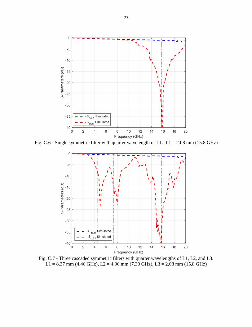
77
Fig. C.6 - Single symmetric filter with quarter wavelength of L1. L1 = 2.08 mm (15.8 GHz)
Fig. C.7 - Three cascaded symmetric filters with quarter wavelengths of L1, L2, and L3.
L1 = 8.37 mm (4.46 GHz), L2 = 4.96 mm (7.30 GHz), L3 = 2.08 mm (15.8 GHz)

78
BC-CPW Coaxial Launch:
Fig. C.8 - Single symmetric filter with quarter wavelength L1. L1 = 4.31 mm (8.14 GHz)
Fig. C.9 - Single symmetric filter with quarter wavelength L1. L1 = 2.93 mm (11.4 GHz)

79
Fig. C.10 - Single symmetric filter with quarter wavelength L1. L1 = 1.79 mm (17.1 GHz)
Fig. C.11 - Three cascaded symmetric filters with quarter wavelengths L1, L2, and L3.
L1 = 4.31 mm (8.14 GHz), L2 = 2.93 mm (11.4 GHz), L3 = 1.79 mm (17.1 GHz)

80
Fig. C.12 - Two cascaded symmetric filters with quarter wavelengths L1 and L2.
L1 = 2.93 mm (11.4 GHz), L2 = 1.79 mm (17.1 GHz)
Fig. C.13 - Single asymmetric filter with quarter wavelengths L1 and L2.
L1 = 2.93 mm (11.4 GHz), L2 = 1.79 mm (17.1 GHz)

81
BC-CPW RF Probe Launch:
Fig. C.11 - Three cascaded symmetric filters with quarter wavelengths L1, L2, and L3.
L1 = 4.31 mm (8.14 GHz), L2 = 2.93 mm (11.4 GHz), L3 = 1.79 mm (17.1 GHz)
Fig. C.15 - Two cascaded symmetric filters with quarter wavelengths L1 and L2.
L1 = 2.93 mm (11.4 GHz), L2 = 1.79 mm (17.1 GHz)

82
Fig. C.16 - Single asymmetric filter with quarter wavelengths L1 and L2.
L1 = 2.93 mm (11.4 GHz), L2 = 1.79 mm (17.1 GHz)