LTC2309
2309fd
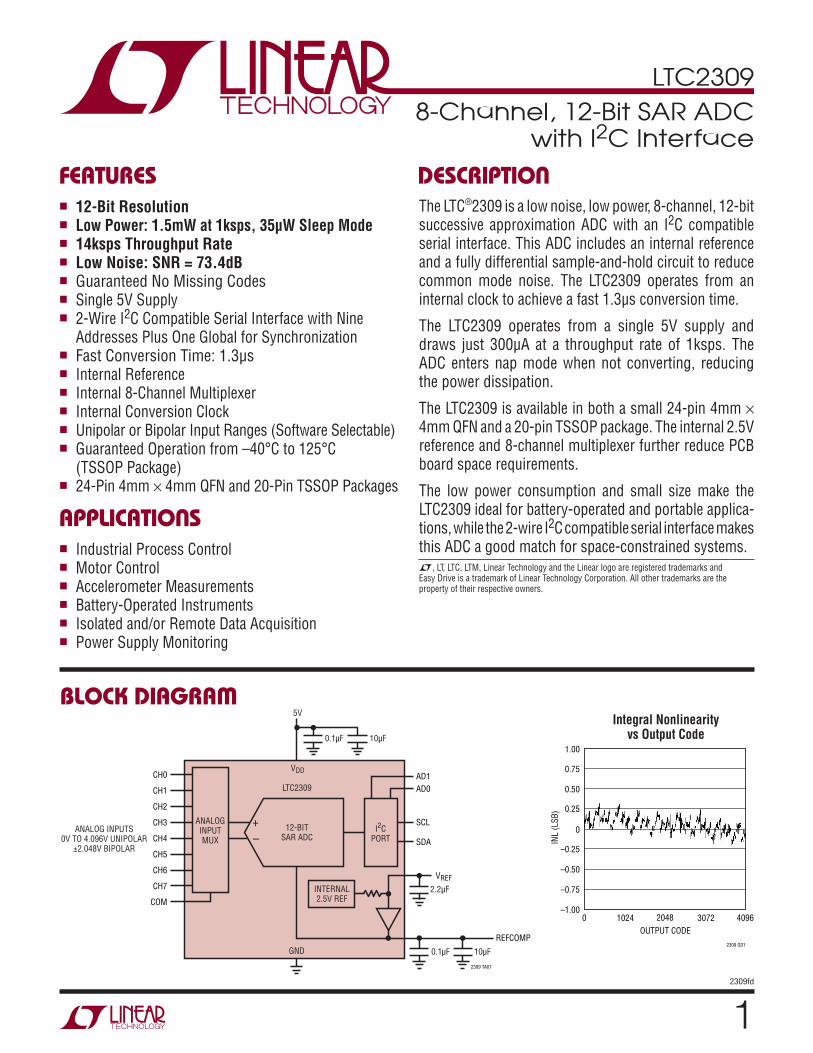
BLOCK DIAGRAM
FeAtuRes
AppLICAtIOns
DesCRIptIOn
8-Channel, 12-Bit SAR ADC with I2C Interface
n IndustrialProcessControln MotorControln AccelerometerMeasurementsn Battery-OperatedInstrumentsn Isolatedand/orRemoteDataAcquisitionn PowerSupplyMonitoring
Integral Nonlinearity vs Output Code
n 12-Bit Resolutionn Low Power: 1.5mW at 1ksps, 35µW Sleep Moden 14ksps Throughput Raten Low Noise: SNR = 73.4dBn GuaranteedNoMissingCodesn Single5VSupplyn 2-WireI2CCompatibleSerialInterfacewithNine
AddressesPlusOneGlobalforSynchronizationn FastConversionTime:1.3µsn InternalReferencen Internal8-ChannelMultiplexern InternalConversionClockn UnipolarorBipolarInputRanges(SoftwareSelectable)n GuaranteedOperationfrom–40°Cto125°C
(TSSOPPackage)n 24-Pin4mm×4mmQFNand20-PinTSSOPPackages
TheLTC®2309isalownoise,lowpower,8-channel,12-bitsuccessive approximation ADC with an I2C compatibleserialinterface.ThisADCincludesaninternalreferenceandafullydifferentialsample-and-holdcircuittoreducecommon mode noise. The LTC2309 operates from aninternalclocktoachieveafast1.3µsconversiontime.
The LTC2309 operates from a single 5V supply anddraws just 300µA at a throughput rate of 1ksps. TheADCentersnapmodewhennot converting, reducingthepowerdissipation.
TheLTC2309isavailableinbothasmall24-pin4mm×4mmQFNanda20-pinTSSOPpackage.Theinternal2.5Vreferenceand8-channelmultiplexerfurtherreducePCBboardspacerequirements.
The low power consumption and small size make theLTC2309idealforbattery-operatedandportableapplica-tions,whilethe2-wireI2CcompatibleserialinterfacemakesthisADCagoodmatchforspace-constrainedsystems.L,LT,LTC,LTM,LinearTechnologyandtheLinearlogoareregisteredtrademarksandEasyDriveisatrademarkofLinearTechnologyCorporation.Allothertrademarksarethepropertyoftheirrespectiveowners.
CH0
CH1
CH2
CH3
CH4
CH5
CH6
CH7
COM
2309 TA01
I2CPORT
ANALOGINPUTMUX
ANALOG INPUTS0V TO 4.096V UNIPOLAR
±2.048V BIPOLAR
REFCOMP
INTERNAL2.5V REF
VDD
5V
GND
LTC2309
0.1µF
12-BITSAR ADC
+–
2.2µF
10µF0.1µF
10µF
VREF
SDA
SCL
AD1AD0
OUTPUT CODE0
INL
(LSB
)
0
0.25
0.50
4096
2309 G01
–0.25
–0.50
–1.001024 2048 3072
–0.75
1.00
0.75

LTC2309
2309fd
ABsOLute MAxIMuM RAtInGs (Notes 1, 2)
ORDeR InFORMAtIOnLEAD FREE FINISH TAPE AND REEL PART MARKING* PACKAGE DESCRIPTION TEMPERATURE RANGE
LTC2309CUF#PBF LTC2309CUF#TRPBF 2309 24-Lead(4mm×4mm)PlasticQFN 0°Cto70°C
LTC2309IUF#PBF LTC2309IUF#TRPBF 2309 24-Lead(4mm×4mm)PlasticQFN –40°Cto85°C
LTC2309CF#PBF LTC2309CF#TRPBF LTC2309F 20-LeadPlasticTSSOP 0°Cto70°C
LTC2309IF#PBF LTC2309IF#TRPBF LTC2309F 20-LeadPlasticTSSOP –40°Cto85°C
LTC2309HF#PBF LTC2309HF#TRPBF LTC2309F 20-LeadPlasticTSSOP –40°Cto125°C
ConsultLTCMarketingforpartsspecifiedwithwideroperatingtemperatureranges.*Thetemperaturegradeisidentifiedbyalabelontheshippingcontainer.ConsultLTCMarketingforinformationonnon-standardleadbasedfinishparts.Formoreinformationonleadfreepartmarking,goto:http://www.linear.com/leadfree/Formoreinformationontapeandreelspecifications,goto:http://www.linear.com/tapeandreel/
SupplyVoltage VDD.......................................................... –0.3Vto6VAnalogInputVoltage(Note3) CH0-CH7,COM,VREF, REFCOMP.................... (GND–0.3V)to(VDD+0.3V)DigitalInputVoltage(Note3)............................ (GND–0.3V)to(VDD+0.3V)DigitalOutputVoltage...... (GND–0.3V)to(VDD+0.3V)
PowerDissipation.............................................. 500mWOperatingTemperatureRange LTC2309C................................................ 0°Cto70°C LTC2309I.............................................–40°Cto85°C LTC2309H.......................................... –40°Cto125°CStorageTemperatureRange.................. –65°Cto150°CLeadTemperature(Soldering,10sec) TSSOP.............................................................. 300°C
24
25
23 22 21 20 19
7 8 9
TOP VIEW
UF PACKAGE24-LEAD (4mm 4mm) PLASTIC QFN
10 11 12
6
5
4
3
2
1
13
14
15
16
17
18CH3
CH4
CH5
CH6
CH7
COM
GND
SDA
SCL
AD1
AD0
VDD
CH2
CH1
CH0
V DD
GND
GND
V REF
REFC
OMP
GND
GND
GND
V DD
TJMAX=150°C,θJA=37°C/W
EXPOSEDPAD(PIN25)ISGND,MUSTBESOLDEREDTOPCB
F PACKAGE20-LEAD PLASTIC TSSOP
1
2
3
4
5
6
7
8
9
10
TOP VIEW
20
19
18
17
16
15
14
13
12
11
REFCOMP
GND
VDD
AD0
AD1
SCL
SDA
GND
GND
VDD
VREF
COM
CH7
CH6
CH5
CH4
CH3
CH2
CH1
CH0
TJMAX=150°C,θJA=90°C/W,θJC=20°C/W
pIn COnFIGuRAtIOn

LTC2309
2309fd
COnVeRteR AnD MuLtIpLexeR CHARACteRIstICsPARAMETER CONDITIONS MIN TYP MAX UNITSResolution(NoMissingCodes) l 12 BitsIntegralLinearityError (Note6) l ±0.45 ±1 LSBDifferentialLinearityError l ±0.35 ±1 LSBBipolarZeroError (Note7) l ±1 ±8 LSBBipolarZeroErrorDrift 0.002 LSB/°CBipolarZeroErrorMatch ±0.1 ±3 LSBUnipolarZeroError (Note7) l ±0.4 ±6 LSBUnipolarZeroErrorDrift 0.002 LSB/°CUnipolarZeroErrorMatch ±0.2 ±1 LSBBipolarFull-ScaleError ExternalReference(Note8)
REFCOMP=4.096Vl
l
±0.5±0.4
±10±9
LSBLSB
BipolarFull-ScaleErrorDrift ExternalReference 0.05 LSB/°CBipolarFull-ScaleErrorMatch ±0.4 ±3 LSBUnipolarFull-ScaleError QFNExternalReference(Note8)
TSSOPExternalReference(Note8)l
l
±0.4±0.5
±10±12
LSBLSB
REFCOMP=4.096V l ±0.3 ±6 LSBUnipolarFull-ScaleErrorDrift ExternalReference 0.05 LSB/°CUnipolarFull-ScaleErrorMatch ±0.3 ±2 LSB
The l denotes the specifications which apply over the full operating temperature range, otherwise specifications are at TA = 25°C. (Notes 4, 5)
SYMBOL PARAMETER CONDITIONS MIN TYP MAX UNITSVIN
+ AbsoluteInputRange(CH0toCH7) (Note9) l –0.05 REFCOMP VVIN
– AbsoluteInputRange(CH0toCH7,COM) Unipolar(Note9)Bipolar(Note9)
l
l
–0.05–0.05
0.25•REFCOMP0.75•REFCOMP
VV
VIN+–VIN
– InputDifferentialVoltageRange VIN=VIN+–VIN
–(Unipolar)VIN=VIN
+–VIN–(Bipolar)
l
l
0toREFCOMP±REFCOMP/2
VV
IIN AnalogInputLeakageCurrent l ±1 µACIN AnalogInputCapacitance SampleMode
HoldMode555
pFpF
CMRR InputCommonModeRejectionRatio 70 dB
AnALOG Input The l denotes the specifications which apply over the full operating temperature range, otherwise specifications are at TA = 25°C. (Note 4)
SYMBOL PARAMETER CONDITIONS MIN TYP MAX UNITSSINAD Signal-to-(Noise+Distortion)Ratio fIN=1kHz l 71 73.3 dBSNR Signal-to-NoiseRatio fIN=1kHz l 71 73.4 dBTHD TotalHarmonicDistortion fIN=1kHz,First5Harmonics l –88 –77 dBSFDR SpuriousFreeDynamicRange fIN=1kHz l 79 90 dB
Channel-to-ChannelIsolation fIN=1kHz –109 dBFullLinearBandwidth (Note11) 700 kHz–3dBInputLinearBandwidth 25 MHzApertureDelay 13 nsTransientResponse Full-ScaleStep 240 ns
DYnAMIC ACCuRACY The l denotes the specifications which apply over the full operating temperature range, otherwise specifications are at TA = 25°C. AIN = –1dBFS. (Notes 4, 10)

LTC2309
2309fd
pOWeR ReQuIReMents
PARAMETER CONDITIONS MIN TYP MAX UNITSVREFOutputVoltage IOUT=0(QFN)
IOUT=0(TSSOP)l
l
2.472.46
2.502.50
2.532.54
VV
VREFOutputTempco IOUT=0 ±25 ppm/°CVREFOutputImpedance –0.1mA≤IOUT≤0.1mA 8 kΩVREFCOMPOutputVoltage IOUT=0 4.096 VVREFLineRegulation VDD=4.75Vto5.25V 0.8 mV/V
InteRnAL ReFeRenCe CHARACteRIstICs The l denotes the specifications which apply over the full operating temperature range, otherwise specifications are at TA = 25°C. (Note 4)
I2C Inputs AnD DIGItAL Outputs The l denotes the specifications which apply over the full operating temperature range, otherwise specifications are at TA = 25°C. (Note 4)
SYMBOL PARAMETER CONDITIONS MIN TYP MAX UNITSVIH HighLevelInputVoltage l 2.85 VVIL LowLevelInputVoltage l 1.5 VVIHA HighLevelInputVoltageforAddressPinsA1,A0 l 4.75 VVILA LowLevelInputVoltageforAddressPinsA1,A0 l 0.25 VRINH ResistancefromA1,A0,toVDDtoSetChip
AddressBitto1l 10 kΩ
RINL ResistancefromA1,A0toGNDtoSetChipAddressBitto0
l 10 kΩ
RINF ResistancefromA1,A0toGNDorVDDtoSetChipAddressBittoFloat
l 2 MΩ
II DigitalInputCurrent VIN=VDD l –10 10 µAVHYS HysteresisofSchmittTriggerInputs (Note9) l 0.25 VVOL LowLevelOutputVoltage(SDA) I=3mA l 0.4 VtOF OutputFallTimeVHtoVIL(MAX) (Note12) l 20+0.1CB 250 nstSP InputSpikeSuppression l 50 nsCCAX ExternalCapacitanceLoadOn-ChipAddressPins
(A1,A0)forValidFloatl 10 pF
SYMBOL PARAMETER CONDITIONS MIN TYP MAX UNITSVDD SupplyVoltage l 4.75 5 5.25 VIDD SupplyCurrent 14kspsSampleRate l 2.3 3 mA
NapMode SLPBit=0,ConversionDone l 210 350 µASleepMode SLPBit=1,ConversionDone l 7 15 µA
PD PowerDissipation 14kspsSampleRate l 11.5 15 mWNapMode SLPBit=0,ConversionDone l 1.05 1.75 mWSleepMode SLPBit=1,ConversionDone l 35 75 µW
The l denotes the specifications which apply over the full operating temperature range, otherwise specifications are at TA = 25°C. (Note 4)

LTC2309
2309fd
I2C tIMInG CHARACteRIstICs The l denotes the specifications which apply over the full operating temperature range, otherwise specifications are at TA = 25°C. (Note 4)
SYMBOL PARAMETER CONDITIONS MIN TYP MAX UNITSfSCL SCLClockFrequency l 400 kHztHD(SDA) HoldTime(Repeated)STARTCondition l 0.6 µstLOW LOWPeriodoftheSCLPin l 1.3 µstHIGH HIGHPeriodoftheSCLPin l 0.6 µstSU(STA) Set-UpTimeforaRepeatedSTARTCondition l 0.6 µstHD(DAT) DataHoldTime l 0 0.9 µstSU(DAT) DataSet-UpTime l 100 nstr RiseTimeforSDA/SCLSignals (Note12) l 20+0.1CB 300 nstf FallTimeforSDA/SCLSignals (Note12) l 20+0.1CB 300 nstSU(STO) Set-UpTimeforSTOPCondition l 0.6 µstBUF BusFreeTimeBetweenaSTOPandSTARTCondition l 1.3 µs
ADC tIMInG CHARACteRIstICs The l denotes the specifications which apply over the full operating temperature range, otherwise specifications are at TA = 25°C. (Note 4)
SYMBOL PARAMETER CONDITIONS MIN TYP MAX UNITSfSMPL ThroughputRate(SuccessiveReads) l 14 kspstCONV ConversionTime (Note9) l 1.3 1.8 µstACQ AcquisitionTime (Note9) l 240 nstREFWAKE REFCOMPWake-UpTime(Note13) CREFCOMP=10µF,CREF=2.2µF 200 ms
Note 1:StressesbeyondthoselistedunderAbsoluteMaximumRatingsmaycausepermanentdamagetothedevice.ExposuretoanyAbsoluteMaximumRatingconditionforextendedperiodsmayaffectdevicereliabilityandlifetime.Note 2:Allvoltagevaluesarewithrespecttoground.Note 3:WhenthesepinvoltagesaretakenbelowgroundoraboveVDD,theywillbeclampedbyinternaldiodes.Theseproductscanhandleinputcurrentsgreaterthan100mAbelowgroundoraboveVDDwithoutlatchup.Note 4:VDD=5V,fSMPL=14kspsinternalreferenceunlessotherwisenoted.Note 5:Linearity,offsetandfull-scalespecificationsapplyforasingle-endedanaloginputwithrespecttoCOM.Note 6:Integralnonlinearityisdefinedasthedeviationofacodefromastraightlinepassingthroughtheactualendpointsofthetransfercurve.Thedeviationismeasuredfromthecenterofthequantizationband.Note 7:Bipolarzeroerroristheoffsetvoltagemeasuredfrom–0.5LSBwhentheoutputcodeflickersbetween000000000000and11111111
1111.Unipolarzeroerroristheoffsetvoltagemeasuredfrom+0.5LSBwhentheoutputcodeflickersbetween000000000000and000000000001.Note 8:Full-scalebipolarerroristheworst-caseof–FSor+FSuntrimmeddeviationfromidealfirstandlastcodetransitionsandincludestheeffectofoffseterror.Unipolarfull-scaleerroristhedeviationofthelastcodetransitionfromidealandincludestheeffectofoffseterror.Note 9:Guaranteedbydesign,notsubjecttotest.Note 10:AllspecificationsindBarereferredtoafull-scale±2.048Vinputwitha2.5Vreferencevoltage.Note 11:Fulllinearbandwidthisdefinedasthefull-scaleinputfrequencyatwhichtheSINADdegradesto60dBor10bitsofaccuracy.Note 12:CB=capacitanceofonebuslineinpF(10pF≤CB≤400pF).Note 13:REFCOMPwake-uptimeisthetimerequiredfortheREFCOMPpintosettlewithin0.5LSBat12-bitresolutionofitsfinalvalueafterwakingupfromSLEEPmode.

LTC2309
2309fd
tYpICAL peRFORMAnCe CHARACteRIstICs
Integral Nonlinearity vs Output Code
1kHz Sine Wave 8192 Point FFT Plot
Supply Current vs Sampling Frequency Offset Error vs Temperature Full-Scale Error vs Temperature
Supply Current vs Temperature Sleep Current vs TemperatureAnalog Input Leakage Current vs Temperature
TA = 25°C, VDD = 5V, fSMPL = 14ksps, unless otherwise noted.
Differential Nonlinearity vs Output Code
OUTPUT CODE0
INL
(LSB
)
0
0.25
0.50
4096
2309 G01
–0.25
–0.50
–1.001024 2048 3072
–0.75
1.00
0.75
OUTPUT CODE0
DNL
(LSB
)0
0.25
0.50
4096
2309 G02
–0.25
–0.50
–1.001024 2048 3072
–0.75
1.00
0.75
FREQUENCY (kHz)0
–140
MAG
NITU
DE (d
B)
–120
–100
–80
0
–40
1 3 4 7
2309 G03
–20
–60
2 5 6
SNR = 73.4dBSINAD = 73.3dBTHD = –88dB
SAMPLING FREQUENCY (ksps)0.1
0
SUPP
LY C
URRE
NT (m
A)
1.5
2.0
2.5
1 10 100
3209 G04
1.0
0.5
TEMPERATURE (°C)–50
OFFS
ET E
RROR
(LSB
)
1.5
25
2309 G05
0
–1.0
–25 0 50
–0.5
–2.0
2.0
1.0
0.5
–0.5
75 100 125
UNIPOLAR
BIPOLAR
TEMPERATURE (°C)–50 –25
–6
FULL
-SCA
LE E
RROR
(LSB
)
–2
4
0 50 75
2309 G06
–4
2
0
25 100 125
UNIPOLAR
BIPOLAR
TEMPERATURE (°C)–50
1.0
SUPP
LY C
URRE
NT (m
A)
1.2
1.6
1.8
2.0
3.0
2.4
0 50 75
2309 G07
1.4
2.6
2.8
2.2
–25 25 100 125TEMPERATURE (°C)
–500
LEAK
AGE
CURR
ENT
(nA)
100
300
400
500
1000
700
0 50 75
2309 G09
200
800
900
600
–25 25 100 125
CH (ON)
CH (OFF)
TEMPERATURE (°C)–50 –25
0
SLEE
P CU
RREN
T (µ
A)
4
10
0 50 75
2309 G08
2
8
6
25 100 125

LTC2309
2309fd
pIn FunCtIOnsCH3-CH7 (Pins 1-5):Channel3toChannel7AnalogInputs.CH3-CH7canbeconfiguredassingle-endedor differential input channels. See the Analog InputMultiplexersection.
COM (Pin 6): Common Input. This is the referencepoint for all single-ended inputs. It must be free ofnoiseandshouldbeconnectedtogroundforunipolarconversionsandmidwaybetweenGNDandREFCOMPforbipolarconversions.
VREF (Pin 7):2.5VReferenceOutput.BypasstoGNDwithaminimum2.2µFceramiccapacitor.Theinternalreferencemaybeoverdrivenbyanexternal2.5Vrefer-enceatthispin.
REFCOMP (Pin 8):ReferenceBufferOutput.Bypassto GND with 10µF and 0.1µF ceramic capacitors inparallel.Nominaloutputvoltageis4.096V.Theinternalreferencebufferdrivingthispinisdisabledbyground-ingVREF,allowingREFCOMPtobeoverdrivenbyanexternalsource.
GND (Pins 9-11, 18-20):Ground.AllGNDpinsmustbeconnectedtoasolidgroundplane.
VDD (Pins 12, 13, 21):5VSupply.TherangeofVDDis4.75Vto5.25V.BypassVDDtoGNDwitha10µFceramiccapacitorinparallelwiththree0.1µFceramiccapacitors,onelocatedascloseaspossibletoeachpin.
AD0 (Pin 14):ChipAddressControlPin.Thispin isconfiguredasathree-state(LOW,HIGH,floating)ad-dresscontrolbitforthedeviceI2Caddress.SeeTable2foraddressselection.
AD1 (Pin 15):ChipAddressControlPin.Thispin isconfigured as a three-state (LOW, HIGH, floating)address control bit for the device I2C address. SeeTable2foraddressselection.
SCL (Pin 16):SerialClockPinoftheI2CInterface.TheLTC2309canonlyactasaslaveandtheSCLpinonlyaccepts anexternal serial clock.Data is shifted intotheSDApinontherisingedgesoftheSCLclockandoutputthroughtheSDApinonthefallingedgesoftheSCLclock.
SDA (Pin 17):BidirectionalSerialDataLineoftheI2CInterface.Intransmittermode(read),theconversionresultisoutputattheSDApin,whileinreceivermode(write),theDINwordisinputattheSDApintocon-figuretheADC.Thepinishighimpedanceduringthedatainputmodeandisanopen-drainoutput(requiresanappropriatepull-updevicetoVDD)duringthedataoutputmode.
CH0-CH2 (Pins 22-24):Channel0toChannel2AnalogInputs.CH0-CH2canbeconfiguredassingle-endedor differential input channels. See the Analog InputMultiplexersection.
Exposed Pad (Pin 25): Ground. Must be soldereddirectlytogroundplane.
(QFN)

LTC2309
2309fd
pIn FunCtIOnsREFCOMP (Pin 1):ReferenceBufferOutput.Bypassto GND with 10µF and 0.1µF ceramic capacitors inparallel.Nominaloutputvoltageis4.096V.Theinternalreferencebufferdrivingthispinisdisabledbyground-ingVREF,allowingREFCOMPtobeoverdrivenbyanexternalsource.
GND (Pins 2, 8 , 9):Ground.AllGNDpinsmustbeconnectedtoasolidgroundplane.
VDD (Pins 3, 10):5VSupply.TherangeofVDDis4.75Vto5.25V.BypassVDDtoGNDwitha10µFceramicca-pacitorinparallelwithtwo0.1µFceramiccapacitors,onelocatedascloseaspossibletoeachpin.
AD0 (Pin 4):ChipAddressControlPin.Thispiniscon-figuredasathree-state(LOW,HIGH,floating)addresscontrolbitforthedeviceI2Caddress.SeeTable2foraddressselection.
AD1 (Pin 5): Chip Address Control Pin. This pin isconfigured as a three-state (LOW, HIGH, floating)address control bit for the device I2C address. SeeTable2foraddressselection.
SCL (Pin 6):SerialClockPinoftheI2CInterface.TheLTC2309canonlyactasaslaveandtheSCLpinonlyaccepts anexternal serial clock.Data is shifted intotheSDApinontherisingedgesoftheSCLclockandoutputthroughtheSDApinonthefallingedgesoftheSCLclock.
SDA (Pin 7):BidirectionalSerialDataLineoftheI2CInterface.Intransmittermode(read),theconversionresultisoutputattheSDApin,whileinreceivermode(write),theDINwordisinputattheSDApintocon-figuretheADC.Thepinishighimpedanceduringthedatainputmodeandisanopen-drainoutput(requiresanappropriatepull-updevicetoVDD)duringthedataoutputmode.
CH0-CH7 (Pins 11-18):Channel0toChannel7AnalogInputs.CH0-CH7canbeconfiguredassingle-endedor differential input channels. See the Analog InputMultiplexersection.
COM (Pin 19):CommonInput.Thisisthereferencepoint for all single-ended inputs. It must be free ofnoiseandshouldbeconnectedtogroundforunipolarconversionsandmidwaybetweenGNDandREFCOMPforbipolarconversions.
VREF (Pin 20):2.5VReferenceOutput.BypasstoGNDwithaminimum2.2µFceramiccapacitor.Theinternalreferencemaybeoverdrivenbyanexternal2.5Vrefer-enceatthispin.
(TSSOP)

LTC2309
2309fd
FunCtIOnAL BLOCK DIAGRAM
CH0
CH1
CH2
CH3
CH4
CH5
CH6
CH7
COM
2308 BD
I2CPORT
ANALOGINPUTMUX
REFCOMP
INTERNAL2.5V REF
VDD
GND
12-BITSAR ADC
LTC2309
8k
GAIN = 1.6384x
+–
VREF
SDA
SCL
AD1AD0
tIMInG DIAGRAM
Definition of Timing for Fast/Standard Mode Devices on the I2C Bus
SDA
SCL
S Sr P StHD(SDA)
S = START, Sr = REPEATED START, P = STOP
tHD(DAT)tSU(STA) tSU(STO)
tSU(DAT)tLOW tHD(SDA)tSP
tBUFtr tf trtf
tHIGH 2309 TD

LTC2309
02309fd
AppLICAtIOns InFORMAtIOnOverview
TheLTC2309isalownoise,8-channel,12-bitsucces-siveapproximationregister(SAR)A/DconverterwithanI2Ccompatibleserialinterface.TheLTC2309includesaprecisioninternalreferenceandaconfigurable8-chan-nelanaloginputmultiplexer(MUX).TheADCmaybeconfiguredtoacceptsingle-endedordifferentialsignalsandcanoperateineitherunipolarorbipolarmode.Asleepmodeoptionisalsoprovidedtofurtherreducepowerduringinactiveperiods.
The LTC2309 communicates through a 2-wire I2Ccompatibleserial interface.Conversionsare initiatedbysignalingaSTOPconditionaftertheparthasbeensuccessfullyaddressedforaread/writeoperation.Thedevicewillnotacknowledge(NACK)anexternalrequestuntiltheconversionisfinished.Afteraconversionisfinished, the device is ready to accept a read/writerequest. Once the LTC2309 is addressed for a readoperation, the device begins outputting the conver-sionresultunderthecontroloftheserialclock(SCL).Thereisnolatencyintheconversionresult.Thereare12bitsofoutputdatafollowedby4trailingzeros.Dataisupdatedonthe fallingedgesofSCL,allowingtheusertoreliablylatchdataontherisingedgeofSCL.AwriteoperationmayfollowthereadoperationbyusingarepeatSTARToraSTOPconditionmaybegiventostartanewconversion.Byselectingawriteoperation,theADCcanbeprogrammedwitha6-bitDINword.TheDINwordconfigurestheMUXandprogramsvariousmodesofoperationoftheADC.
During a conversion, the internal 12-bit capacitivechargeredistributionDACoutputissequencedthroughasuccessiveapproximationalgorithmbytheSARstart-ing from themostsignificantbit (MSB) to the leastsignificantbit(LSB).ThesampledinputissuccessivelycomparedwithbinaryweightedchargessuppliedbythecapacitiveDACusingadifferentialcomparator.Attheendofaconversion,theDACoutputbalancestheanaloginput.TheSARcontents(a12-bitdataword)thatrepresentthesampledanaloginputareloadedinto12outputlatchesthatallowthedatatobeshiftedoutviatheI2Cinterface.
Programming the LTC2309
Thevariousmodesofoperationof theLTC2309areprogrammedbya6-bitDINword.TheSDIinputdatabitsareloadedontherisingedgeofSCLduringawriteoperation,withtheS/DbitloadedonthefirstrisingedgeandtheSLPbitonthesixthrisingedge(seeFigure8bin the I2C Interfacesection).The inputdataword isdefinedasfollows:
S/D O/S S1 S0 UNI SLP
S/D=SINGLE-ENDED/DIFFERENTIALBIT
O/S=ODD/SIGNBIT
S1=CHANNELSELECTBIT1
S0=CHANNELSELECTBIT0
UNI=UNIPOLAR/BIPOLARBIT
SLP=SLEEPMODEBIT
Analog Input Multiplexer
The analog input MUX is programmed by the S/D,O/S,S1andS0bitsoftheDINword.Table1liststheMUXconfigurationsforallcombinationsofthecon-figurationbits.Figure1ashowsseveralpossibleMUXconfigurationsandFigure1bshowshowtheMUXcanbereconfiguredfromoneconversiontothenext.
Driving the Analog Inputs
Theanalog inputsof theLTC2309areeasy todrive.Eachoftheanaloginputscanbeusedasasingle-endedinputrelativetotheCOMpin(CH0-COM,CH1-COM,etc.)orindifferentialinputpairs(CH0andCH1,CH2andCH3,CH4andCH5,CH6andCH7).Figure2showshowtodriveCOMforsingle-endedinputsinunipolarandbipolarmodes.RegardlessoftheMUXconfigura-tion,the“+”and“–”inputsaresampledatthesameinstant.Anyunwantedsignalthatiscommontobothinputswillbereducedbythecommonmoderejectionofthesample-and-holdcircuit.Theinputsdrawonlyonesmallcurrentspikewhilechargingthesample-and-holdcapacitorsduringtheacquiremode.Inconversion

LTC2309
2309fd
AppLICAtIOns InFORMAtIOn
CH0CH1CH2CH3CH4CH5CH6CH7
COM (–)
8 Single-Ended
+++++++
4 Differential
+ (–) +
+ (–)
+ (–)
+ (–)– (+)
– (+)
– (+)
– (+)
COM (–)
Combinations of Differential and Single-Ended
+++++
+––
2309 F01a
CH0CH1
CH2CH3
CH4CH5
CH6CH7
CH0CH1
CH2CH3
CH4CH5CH6CH7
Table 1. Channel ConfigurationS/D O/S S1 S0 0 1 2 3 4 5 6 7 COM
0 0 0 0 + –0 0 0 1 + –0 0 1 0 + –0 0 1 1 + –0 1 0 0 – +0 1 0 1 – +0 1 1 0 – +0 1 1 1 – +1 0 0 0 + –1 0 0 1 + –1 0 1 0 + –1 0 1 1 + –1 1 0 0 + –1 1 0 1 + –1 1 1 0 + –1 1 1 1 + –
COM(UNUSED)
COM (–)
1st Conversion 2nd Conversion
+–+–
+–
++
CH2CH3
CH4CH5
CH2CH3
CH4CH5
2328 F01b
COM COM
REFCOMP/2
Unipolar Mode Bipolar Mode
2328 F02
+–
Figure 1a. Example of MUX Configurations
Figure 1b. Changing the MUX Assignments “On the Fly”
Figure 2. Driving COM in Unipolar and Bipolar Modes
mode,theanaloginputsdrawonlyasmallleakagecur-rent.Ifthesourceimpedanceofthedrivingcircuitislow,theADCinputscanbedrivendirectly.Otherwise,moreacquisitiontimeshouldbeallowedforasourcewithhigherimpedance.
Input Filtering
The noise and distortion of the input amplifier andothercircuitrymustbeconsideredsincetheywilladdtotheADCnoiseanddistortion.Therefore,noisyinputcircuitryshouldbefilteredpriortotheanaloginputstominimizenoise.Asimple1-poleRCfilterissufficientformanyapplications.
TheanaloginputsoftheLTC2309canbemodeledasa55pFcapacitor(CIN)inserieswitha100Ωresistor(RON),asshowninFigure3a.CINgetsswitchedtotheselectedinputonceduringeachconversion.LargefilterRCtimeconstantswillslowthesettlingoftheinputs.It is importantthattheoverallRCtimeconstantsbeshortenoughtoallowtheanaloginputstocompletelysettleto12-bitresolutionwithintheacquisitiontime(tACQ)ifDCaccuracyisimportant.

LTC2309
2309fd
AppLICAtIOns InFORMAtIOnWhenusingafilterwithalargeCFILTERvalue(e.g.1µF),theinputsdonotcompletelysettleandthecapacitiveinputswitchingcurrentsareaveraged intoanetDCcurrent(IDC).Inthiscase,theanaloginputcanbemod-eledbyanequivalentresistance(REQ=1/(fSMPL•CIN))inserieswithanidealvoltagesource(VREFCOMP/2),asshowninFigure3b.ThemagnitudeoftheDCcurrentisthenapproximatelyIDC=(VIN–VREFCOMP/2)/REQ,whichisroughlyproportionaltoVIN.TopreventlargeDCdropsacrosstheresistorRFILTER,afilterwithasmallresistorandlargecapacitorshouldbechosen.Whenrunningatthemaximumthroughputrateof14ksps,theinputcurrentequals1.5µAatVIN=4.096V,whichamountstoafull-scaleerrorof0.5LSBwhenusingafilterresistor(RFILTER)of333Ω.Applicationsrequiringlowersampleratescantoleratealargerfilterresistorforthesameamountoffull-scaleerror.
selfheatingandfromdamagethatmayoccurduringsoldering.Metalfilmsurfacemountresistorsaremuchlesssusceptibletobothproblems.
Dynamic Performance
FastFourierTransform(FFT)testtechniquesareusedtotesttheADC’sfrequencyresponse,distortionandnoiseattheratedthroughput.ByapplyingalowdistortionsinewaveandanalyzingthedigitaloutputusinganFFTalgorithm,theADC’sspectralcontentcanbeexaminedforfrequenciesoutsidethefundamental.
Signal-to-Noise and Distortion Ratio (SINAD)
Thesignal-to-noiseanddistortionratio(SINAD)istheratiobetweentheRMSamplitudeofthefundamentalinputfrequencytotheRMSamplitudeofallotherfre-quencycomponentsattheA/Doutput.Theoutputisband-limitedtofrequenciesfromaboveDCandbelowhalfthesamplingfrequency.Figure5showsatypicalSINADof73.3dBwitha14kHzsampling rateanda1kHzinput.AnSNRof73.4dBcanbeachievedwiththeLTC2309.
VIN
INPUTCH0-CH7 RON
100Ω
CIN55pFCFILTER
RSOURCE
2309 F03a
LTC2309
Figure 3a. Analog Input Equivalent Circuit
VIN
INPUTCH0-CH7
REQ1/(fSMPL • CIN)
VREFCOMP/2
CFILTER
RFILTERIDC
2309 F03b
LTC2309
+–
Figure 3b. Analog Input Equivalent Circuit for Large Filter Capacitances
Figures4aand4bshowexamplesofinputfilteringforsingle-ended and differential inputs. For the single-endedcaseinFigure4a,a50Ωsourceresistoranda2000pFcapacitortogroundontheinputwilllimittheinputbandwidthto1.6MHz.HighqualitycapacitorsandresistorsshouldbeusedintheRCfiltersincethesecomponentscanadddistortion.NPOandsilvermicatypedielectriccapacitorshaveexcellentlinearity.Carbonsurfacemountresistorscangeneratedistortionfrom
2309 F04a
CH0
COM
LTC2309
REFCOMP
2000pF
0.1µF 10µF
50ΩANALOGINPUT
Figure 4a. Optional RC Input Filtering for Single-Ended Input
1000pF
2309 F04b
CH0
CH1
LTC2309
REFCOMP
1000pF
1000pF
0.1µF 10µF
50Ω
50Ω
DIFFERENTIALANALOGINPUTS
Figure 4b. Optional RC Input Filtering for Differential Inputs

LTC2309
2309fd
Total Harmonic Distortion (THD)
Total harmonic distortion (THD) is the ratio of theRMSsumofallharmonicsoftheinputsignaltothefundamentalitself.Theout-of-bandharmonicsaliasintothefrequencybandbetweenDCandhalfthesamplingfrequency(fSMPL/2).THDisexpressedas:
THD
V V V VV
N=+ + +
20 22
32
42 2
1log
...
where V1 is the RMS amplitude of the fundamentalfrequencyandV2throughVNaretheamplitudesofthesecondthroughNthharmonics.
Internal Reference
The LTC2309 has an on-chip, temperature compen-sated bandgap reference that is factory trimmed to2.5V(RefertoFigure6a).ItisinternallyconnectedtoareferenceamplifierandisavailableatVREF.VREFshouldbebypassedtoGNDwitha2.2μFceramiccapacitortominimizenoise.An8kresistorisinserieswiththeoutputsothatitcanbeeasilyoverdrivenbyanexternalrefer-enceifmoreaccuracyand/orlowerdriftarerequired,asshowninFigure6b.ThereferenceamplifiergainstheVREFvoltageby1.638to4.096VatREFCOMP.Tocompensatethereferenceamplifier,bypassREFCOMPwitha10μFceramiccapacitorinparallelwitha0.1μFceramic capacitor for best noise performance. The
internalreferencebuffercanalsobeoverdrivenfrom1VtoVDD,asshowninFigure6c.Todoso,VREFmustbegroundedtodisablethereferencebuffer.
AppLICAtIOns InFORMAtIOn
Figure 5. 1kHz Sine Wave 8192 Point FFT Plot
R2
R3
REFERENCEAMP
0.1µF
10µF
2.2µF
REFCOMP
GND
VREF
R18k
2.5V
4.096V
LTC2309
2309 F06a
BANDGAPREFERENCE
Figure 6a. LTC2309 Reference Circuit
0.1µF10µF
2309 F06b
LT1790A-2.5VOUT
VIN
5V
VREF
LTC2309
GND
REFCOMP
2.2µF
0.1µF
Figure 6b. Using the LT®1790A-2.5 as an External Reference
FREQUENCY (kHz)0
–140
MAG
NITU
DE (d
B)
–120
–100
–80
0
–40
1 3 4 7
2309 G03
–20
–60
2 5 6
SNR = 73.4dBSINAD = 73.3dBTHD = –88dB
Figure 6c. Overdriving REFCOMP Using the LT1790A-4.096
0.1µF
0.1µF
10µF
2309 F06c
LT1790A-4.096VOUT
VIN
5V
VREF
LTC2309
GND
REFCOMP

LTC2309
2309fd
Internal Conversion Clock
The internal conversion clock is factory trimmed toachieveatypicalconversiontime(tCONV)of1.3μsanda maximum conversion time of 1.8μs over the fulloperatingtemperaturerange.
I2C Interface
TheLTC2309communicatesthroughanI2Cinterface.TheI2Cinterfaceisa2-wireopen-draininterfacesup-porting multiple devices and multiple masters on asinglebus.Theconnecteddevicescanonlypull theserialdataline(SDA)LOWandcanneverdriveitHIGH.SDAisrequiredtobeexternallyconnectedtothesup-plythroughapull-upresistor.WhenthedatalineisnotbeingdrivenLOW,itisHIGH.DataontheI2Cbuscanbetransferredatratesupto100kbits/sinthestandardmodeandupto400kbits/sinthefastmode.TheVDDpowershouldnotberemovedfromtheLTC2309whentheI2CbusisactivetoavoidloadingtheI2CbuslinesthroughtheinternalESDprotectiondiodes.
EachdeviceontheI2Cbusisrecognizedbyauniqueaddressstoredinthedeviceandcanonlyoperateeitherasatransmitterorreceiver,dependingonthefunctionof thedevice.Adevicecanalsobeconsideredasamasteroraslavewhenperformingdatatransfers.Amasteristhedevicewhichinitiatesadatatransferonthebusandgeneratestheclocksignalstopermitthetransfer.Devicesaddressedbythemasterareconsid-eredslaves.
TheLTC2309canonlybeaddressedasaslave(seeTable2).Onceaddressed,itcanreceiveconfigurationbits(DINword)ortransmitthelastconversionresult.Theserialclockline(SCL)isalwaysaninputtotheLTC2309andtheserialdataline(SDA)isbidirectional.Thedevicesupportsthestandardmodeandthefastmodefordatatransferspeedsupto400kbits/s(seetheTimingDiagramsectionfordefinitionoftheI2Ctiming).
The START and STOP Conditions
ReferringtoFigure7,aSTART(S)conditionisgener-atedby transitioningSDA fromHIGH toLOWwhileSCLisHIGH.ThebusisconsideredtobebusyaftertheSTARTcondition.Whenthedatatransferisfinished,aSTOP(P)conditionisgeneratedbytransitioningSDAfromLOWtoHIGHwhileSCLisHIGH.ThebusisfreeafteraSTOPconditionisgenerated.STARTandSTOPconditionsarealwaysgeneratedbythemaster.
When the bus is in use, it stays busy if a repeatedSTART(Sr)isgeneratedinsteadofaSTOPcondition.TherepeatedSTARTtimingisfunctionallyidenticaltotheSTARTandisusedforwritingandreadingfromthedevicebeforetheinitiationofanewconversion.
AppLICAtIOns InFORMAtIOn
S
START Condition STOP Condition
P
2309 F07
SDA
SCL
SDA
SCL
Figure 7. Timing Diagrams of START and STOP Conditions
Data Transferring
After theSTARTcondition, theI2Cbus isbusyanddatatransfercanbeginbetweenthemasterandtheaddressedslave.Dataistransferredoverthebusingroups of nine bits, one byte followed by one ac-knowledge(ACK)bit.Themaster releases theSDAlineduringtheninthSCLclockcycle.TheslavedevicecanissueanACKbypullingSDALOWorissueaNotAcknowledge (NACK) by leaving the SDA line highimpedance(theexternalpull-upresistorwillholdthelinehigh).ChangeofdataonlyoccurswhiletheSCLlineisLOW.
Data Format
After a START condition, the master sends a 7-bitaddressfollowedbyaread/write(R/W)bit.TheR/Wbit is1forareadrequestand0forawriterequest.If the 7-bit address matches one of the LTC2309’s9pin-selectableaddresses,theADCisselected.When

LTC2309
2309fd
AppLICAtIOns InFORMAtIOntheADCisaddressedduringaconversion,itwillnotacknowledgeR/WrequestsandwillissueaNACKbyleavingtheSDAlineHIGH.Iftheconversioniscom-plete,theLTC2309issuesanACKbypullingtheSDAlineLOW.TheLTC2309hastworegisters.The12-bitwideoutputregistercontainsthelastconversionresult.The6-bitwideinputregisterconfigurestheinputMUXandtheoperatingmodeoftheADC.
Output Data Format
Theoutputregistercontainsthelastconversionresult.Aftereachconversioniscompleted,thedeviceauto-maticallyenterseithernaporsleepmodedependingonthesettingoftheSLPbit(seeNapModeandSleepModesections).WhentheLTC2309isaddressedfor
a read operation, it acknowledges by pulling SDALOW and acts as a transmitter. The master/receivercanreadupto twobytes fromtheLTC2309.Afteracompletereadoperationof2bytes,aSTOPconditionisneededtoinitiateanewconversion.ThedevicewillNACKsubsequentreadoperationswhileaconversionisbeingperformed.
Thedataoutputstreamis16bitslongandisshiftedoutonthefallingedgesofSCL(seeFigure8a).ThefirstbitistheMSBandthe12thbitistheLSBoftheconversion result. The remaining four bits are zero.Figures14and15arethetransfercharacteristicsforthebipolarandunipolarmodes.DataisoutputontheSDAlinein2’scomplementformatforbipolarreadingsorinstraightbinaryforunipolarreadings.
1 2
A6SDA
START BYMASTER
ACK BYADC
ACK BYMASTER
NACK BYMASTER
STOPBY MASTER
CONVERSIONINITIATED
SCL
SCL(CONTINUED)
A5 A4 A3 A2 A1 A0 R/W
3 4 5 6 7 8 9 1 2 3 4 5 6 7 8 9
1 2 3 4 5 6 7 8 9
2309 F08a
B11 B10
READ 1 BYTE
B9 B8 B7
MOST SIGNIFICANT DATA BYTE
B6 B5 B4
• • •
• • •
SDA(CONTINUED) • • •
• • •
B3 B2 B1 B0
LEAST SIGNIFICANT DATA BYTE
READ 1 BYTE
ADDRESS FRAME
Figure 8a. Timing Diagram for Reading from the LTC2309

LTC2309
2309fd
Input Data Format
WhentheLTC2309isaddressedforawriteoperation,itacknowledgesbypullingSDALOWduringtheLOWperiodbeforethe9thcycleandactsasareceiver.Themaster/transmittercanthensend1bytetoprogramthedevice.Theinputbyteconsistsofthe6-bitDINwordfollowedbytwobitsthatareignoredbytheADCandare considered don’t cares (X) (see Figure8b). TheinputbitsarelatchedontherisingedgeofSCLduringthewriteoperation.
After power-up, the ADC initiates an internal resetcyclewhichsetstheDINwordtoall0s(S/D=O/S=S0=S1=UNI=SLP=0).AwriteoperationmaybeperformedifthedefaultstateoftheADC’sconfigurationisnotdesired.Otherwise,theADCmustbeproperlyaddressedandfollowedbyaSTOPconditiontoinitiateaconversion.
Initiating a New Conversion
TheLTC2309awakensfromeithernaporsleepwhenproperlyaddressedforaread/writeoperation.ASTOPcommand may then be issued after performing theread/writeoperationtotriggeranewconversion.
IssuingaSTOPcommandafterthe8thSCLclockpulseoftheaddressframeandbeforethecompletionofa
Table 2. Address AssignmentAD1 AD0 ADDRESS
LOW LOW 0001000
LOW Float 0001001
LOW HIGH 0001010
Float HIGH 0001011
Float Float 0011000
Float LOW 0011001
HIGH LOW 0011010
HIGH Float 0011011
HIGH HIGH 0101000
1 2
A6SDA
START BYMASTER
ACK BYADC
ACK BYADC
CONVERSIONINITIATED
STOP BYMASTER
SCL
A5 A4 A3 A2 A1 A0 R/W
3 4 5 6 7 8 9 1 2 3 4 5 6 7 8 9
2309 F08b
S/D O/S
WRITE 1 BYTE
S1 S0 UNI
DIN WORD
SLP X X
ADDRESS FRAME
Figure 8b. Timing Diagram for Writing to the LTC2309
AppLICAtIOns InFORMAtIOnread/writeoperationwillalsoinitiatenewconversion,buttheoutputresultmaynotbevalidduetolackofadequateacquisitiontime(seeAcquisitionsection).
LTC2309 Address
TheLTC2309hastwoaddresspins(AD0andAD1)thatmaybetiedHIGH,LOW,orleftfloatingtoenableoneof9possibleaddresses(seeTable2).
In addition to the configurable addresses listed inTable2, theLTC2309alsocontainsaglobaladdress(1101011)whichmaybeusedforsynchronizingmul-tipleLTC2309sorotherI2CLTC230XSARADCs(seeSynchronizingMultipleLTC2309swithGlobalAddressCallsection).

LTC2309
2309fd
AppLICAtIOns InFORMAtIOnatesaNACKsignalindicatingtheconversioncycleisinprogress.
Continuous Read/Write
Oncetheconversioncycleiscomplete,theLTC2309canbewrittentoandthenreadfromusingtherepeatedSTART(Sr)command.Figure10showsacyclewhichbeginswithadatawrite,arepeatedSTART,followedbyareadandconcludedwithaSTOPcommand.Afterall16bitsarereadout,aconversionmaybeinitiatedbyissuingaSTOPcommand.Thefollowingconver-sionwillbeperformedusingthenewlyprogrammeddata.
S
CONVERSION NAP DATA OUTPUT CONVERSION CONVERSIONNAP DATAOUTPUT
R ACK READ7-BIT ADDRESS P S R ACK
2309 F09
READ7-BIT ADDRESS P
Figure 9. Consecutive Reading with the Same Configuration
Continuous Read
Inapplicationswherethesameinputchannelissampledeachcycle,conversionscanbecontinuouslyperformedandreadwithoutawritecycle(seeFigure9).TheDINwordremainsunchangedfromthelastvaluewrittenintothedevice.Ifthedevicehasnotbeenwrittentosincepower-up,theDINworddefaultstoall0s(S/D=O/S=S0=S1=UNI=SLP=0).Attheendofareadoperation,aSTOPconditionmaybegiventostartanewconversion.Attheconclusionoftheconversioncycle,thenextresultmaybereadusingthemethoddescribedabove.Iftheconversioncycleisnotconcludedandavalidaddressselectsthedevice,theLTC2309gener-
S
CONVERSION NAP DATA INPUT ADDRESS CONVERSIONDATAOUTPUT
W ACK WRITE7-BIT ADDRESS Sr R ACK
2309 F10
READ7-BIT ADDRESS P
Figure 10. Write, Read, START Conversion

LTC2309
2309fd
AppLICAtIOns InFORMAtIOnSynchronizing Multiple LTC2309s with a Global Address Call
InapplicationswhereseveralLTC2309sorotherI2CSARADCsfromLinearTechnologyCorporationareusedonthesameI2Cbus,allconverterscanbesynchronizedthroughtheuseofaglobaladdresscall.Priortoissu-ingtheglobaladdresscall,allconvertersmusthavecompletedaconversioncycle.ThemasterthenissuesaSTART,followedbytheglobaladdress1101011,andawriterequest.Allconverterswillbeselectedandac-knowledgetherequest.Themasterthensendsawritebyte(optional)followedbytheSTOPcommand.Thiswillupdatethechannelselection(optional)andsimultane-ouslyinitiateaconversionforallADCsonthebus(seeFigure11).Inordertosynchronizemultipleconverterswithoutchangingthechannel,aSTOPcommandmaybeissuedafteracknowledgementoftheglobalwritecommand.GlobalreadcommandsarenotallowedandtheconverterswillNACKaglobalreadrequest.
Nap Mode
TheADCentersnapmodeafteraconversioniscom-plete(tCONV)iftheSLPbitissettoalogic0.Thesup-plycurrentdecreasesto210μAinnapmodebetweenconversions, thereby reducing the average powerdissipationasthesampleratedecreases.Forexample,theLTC2309drawsanaverageof300µAata1kspssamplingrate.TheLTC2309keepsonlythereference(VREF)andreferencebuffer(REFCOMP)circuitryactivewheninnapmode.
Sleep Mode
TheADCenterssleepmodeafteraconversioniscom-plete(tCONV)iftheSLPbitissettoalogic1.TheADCdrawsonly7µAinsleepmode,providedthatnoneofthedigitalinputsareswitching.WhentheLTC2309isproperlyaddressed,theADCisreleasedfromsleepmodeandrequires200ms(tREFWAKE)towakeupandchargetherespective2.2μFand10μFbypasscapacitorsontheVREFandREFCOMPpins.Anewconversionshouldnotbeinitiatedbeforethistime,asshowninFigure12.
S
SDA
SCL
CONVERSION NAP
LTC2309
DATA OUTPUT CONVERSION OF ALL LTC2309s
W ACK WRITE (OPTIONAL)GLOBAL ADDRESS P
LTC2309 LTC2309
2309 F11
Figure 11. Synchronous Multiple LTC2309s with a Global Address Call
S
CONVERSION SLEEP tREFWAKE CONVERSION
R/W ACK7-BIT ADDRESS P
2309 F12
Figure 12. Exiting Sleep Mode and Starting a New Conversion
LTC2309
2309fd
AppLICAtIOns InFORMAtIOnAcquisition
TheLTC2309beginsacquiringtheinputsignalatdif-ferentinstancesdependingonwhetherareadorwriteoperation isbeingperformed. If a readoperation isbeingperformed,acquisitionoftheinputsignalbeginsontherisingedgeofthe9thclockpulsefollowingtheaddressframe,asshowninFigure13a.
Ifawriteoperationisbeingperformed,acquisitionoftheinputsignalbeginsonthefallingedgeofthesixthclockcycleaftertheDINwordhasbeenshiftedin,asshown in Figure 13b. The LTC2309 will acquire thesignalfromtheinputchannelthatwasmostrecentlyprogrammedbytheDINword.Aminimumof240nsisrequiredtoacquiretheinputsignalbeforeinitiatinganewconversion.
1 2
A6SDA
SCL
A5 A4 A3 A2 A1 A0 R/W
3 4 5 6 7 8 9 1 2
B11
ACQUISITION BEGINS
tACQ2309 F13a
B10
1 2
A2 A1 A0 R/WSDA
SCL
S/D O/S S1 S0 UNI X X
3 4 55 6 7 8 9 6 7 8 9
ACQUISITION BEGINS
tACQ 2309 F13b
SLP
Figure 13a. Timing Diagram Showing Acquisition During a Read Operation
Figure 13b. Timing Diagram Showing Acquisition During a Write Operation
INPUT VOLTAGE (V)
0V
OUTP
UT C
ODE
(TW
O’S
COM
PLEM
ENT)
–1 LSB
2309 F14
011...111
011...110
000...001
000...000
100...000
100...001
111...110
1LSB
BIPOLARZERO
111...111
FS/2 – 1LSB–FS/2
FS = 4.096V1LSB = FS/212
1LSB = 1mV
INPUT VOLTAGE (V)
OUTP
UT C
ODE
2309 F15
111...111
111...110
100...001
100...000
000...000
000...001
011...110
011...111
FS – 1LSB0V
UNIPOLARZERO
FS = 4.096V1LSB = FS/212
1LSB = 1mV
Figure 14. Bipolar Transfer Characteristics (2’s Complement) Figure 15. Unipolar Transfer Characteristics (Straight Binary)
LTC2309
02309fd
AppLICAtIOns InFORMAtIOn
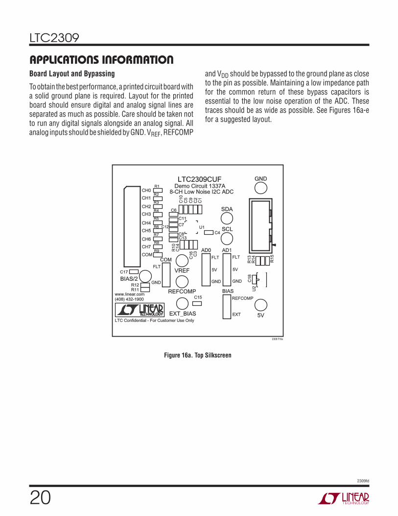
Figure 16a. Top Silkscreen
2309 F16a
Board Layout and Bypassing
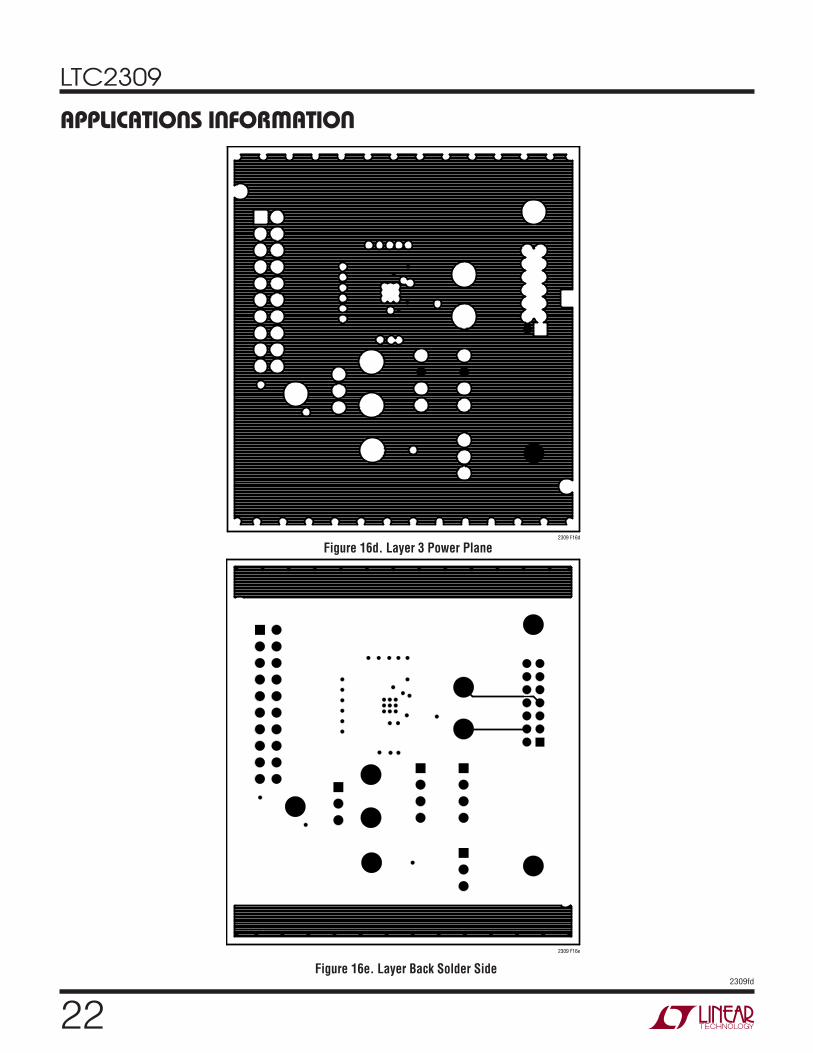
Toobtainthebestperformance,aprintedcircuitboardwithasolidgroundplaneisrequired.Layoutfortheprintedboardshouldensuredigitalandanalogsignal linesareseparatedasmuchaspossible.Careshouldbetakennottorunanydigitalsignalsalongsideananalogsignal.AllanaloginputsshouldbeshieldedbyGND.VREF,REFCOMP
andVDDshouldbebypassedtothegroundplaneasclosetothepinaspossible.Maintainingalowimpedancepathfor the common return of these bypass capacitors isessential to the lownoiseoperationof theADC.Thesetracesshouldbeaswideaspossible.SeeFigures16a-eforasuggestedlayout.

LTC2309
2309fd
2309 F16b
Figure 16b. Layer 1 Component Side
AppLICAtIOns InFORMAtIOn
Figure 16c. Layer 2 Ground Plane2309 F16c
LTC2309
2309fd
AppLICAtIOns InFORMAtIOn
Figure 16d. Layer 3 Power Plane2309 F16d
Figure 16e. Layer Back Solder Side2309 F16e

LTC2309
2309fd
pACKAGe DesCRIptIOnUF Package
24-Lead Plastic QFN (4mm × 4mm)(ReferenceLTCDWG#05-08-1697)
4.00 ± 0.10(4 SIDES)
NOTE:1. DRAWING PROPOSED TO BE MADE A JEDEC PACKAGE OUTLINE MO-220 VARIATION (WGGD-X)—TO BE APPROVED2. DRAWING NOT TO SCALE3. ALL DIMENSIONS ARE IN MILLIMETERS4. DIMENSIONS OF EXPOSED PAD ON BOTTOM OF PACKAGE DO NOT INCLUDE MOLD FLASH. MOLD FLASH, IF PRESENT, SHALL NOT EXCEED 0.15mm ON ANY SIDE, IF PRESENT5. EXPOSED PAD SHALL BE SOLDER PLATED6. SHADED AREA IS ONLY A REFERENCE FOR PIN 1 LOCATION ON THE TOP AND BOTTOM OF PACKAGE
PIN 1TOP MARK(NOTE 6)
0.40 ± 0.10
2423
1
2
BOTTOM VIEW—EXPOSED PAD
2.45 ± 0.10(4-SIDES)
0.75 ± 0.05 R = 0.115TYP
0.25 ± 0.05
0.50 BSC
0.200 REF
0.00 – 0.05
(UF24) QFN 0105
RECOMMENDED SOLDER PAD PITCH AND DIMENSIONS
0.70 ±0.05
0.25 ±0.050.50 BSC
2.45 ± 0.05(4 SIDES)3.10 ± 0.05
4.50 ± 0.05
PACKAGE OUTLINE
PIN 1 NOTCHR = 0.20 TYP OR 0.35 45° CHAMFER

LTC2309
2309fd
F Package20-Lead Plastic TSSOP (4.4mm)(ReferenceLTCDWG#05-08-1650)
F20 TSSOP 0204
0.09 – 0.20(.0035 – .0079)
0° – 8°
0.25REF
0.50 – 0.75(.020 – .030)
4.30 – 4.50**(.169 – .177)
1 3 4 5 6 7 8 9 10
111214 13
6.40 – 6.60*(.252 – .260)
20 19 18 17 16 15
1.10(.0433)
MAX
0.05 – 0.15(.002 – .006)
0.65(.0256)
BSC
6.40(.252)BSC
0.19 – 0.30(.0075 – .0118)
TYP
2
MILLIMETERS(INCHES)
DIMENSIONS DO NOT INCLUDE MOLD FLASH. MOLD FLASH SHALL NOT EXCEED .152mm (.006") PER SIDEDIMENSIONS DO NOT INCLUDE INTERLEAD FLASH. INTERLEADFLASH SHALL NOT EXCEED .254mm (.010") PER SIDE
*
**
NOTE:1. CONTROLLING DIMENSION: MILLIMETERS
2. DIMENSIONS ARE IN
3. DRAWING NOT TO SCALE
RECOMMENDED SOLDER PAD LAYOUT
0.45 ±0.05 0.65 BSC
4.50 ±0.106.60 ±0.10
1.05 ±0.10
pACKAGe DesCRIptIOn

LTC2309
2309fd
Information furnished by Linear Technology Corporation is believed to be accurate and reliable.However,noresponsibilityisassumedforitsuse.LinearTechnologyCorporationmakesnorepresenta-tionthattheinterconnectionofitscircuitsasdescribedhereinwillnotinfringeonexistingpatentrights.
ReVIsIOn HIstORYREV DATE DESCRIPTION PAGE NUMBER
D 7/10 RevisedBlockDiagram 1
ChangedAVDDandDVDDpinstoVDDonly 2,4-9,20
RevisedNote2 5
ConsolidatedAVDDandDVDDintoVDDandrevisedVREFandREFCOMPpindescriptionsinPinFunctionssection 7,8
RevisedFigures6band6candInternalReferenceparagraph,andaddedtexttoI2CInterfaceinApplicationsInformationsection
13,14
ChangedNAKtoNACKinFigure8a 15
RevisedTypicalApplication 26
(Revision history begins at Rev D)

LTC2309
2309fd
Linear Technology Corporation1630 McCarthy Blvd., Milpitas, CA 95035-7417(408)432-1900FAX: (408)434-0507www.linear.com LINEAR TECHNOLOGY CORPORATION 2008
LT 0710 REV D • PRINTED IN USA
ReLAteD pARts
tYpICAL AppLICAtIOn
PART NUMBER DESCRIPTION COMMENTS
LTC1417 14-Bit,400kspsSerialADC 20mW,UnipolarorBipolar,InternalReference,SSOP-16Package
LTC1468/LTC1469 Single/Dual90MHz,22V/µs,16-BitAccurateOpAmps
LowInputOffset:75µV/125µV
LTC1609 16-Bit,200kspsSerialADC 65mW,ConfigurableBipolarandUnipolarInputRanges,5VSupply
LTC1790 MicropowerLowDropoutReference 60µASupplyCurrent,10ppm/°C,SOT-23Package
LTC1850/LTC1851 10-Bit/12-Bit,8-Channel,1.25MspsADCs ParallelOutput,ProgrammableMUXandSequencer,5VSupply
LTC1852/LTC1853 10-Bit/12-Bit,8-Channel,400kspsADCs ParallelOutput,ProgrammableMUXandSequencer,3Vor5VSupply
LTC1860/LTC1861 12-Bit,1-/2-Channel250kspsADCsinMSOP 850µAat250ksps,2µAat1ksps,SO-8andMSOPPackages
LTC1860L/LTC1861L 3V,12-bit,1-/2-Channel150kspsADCs 450µAat150ksps,10µAat1ksps,SO-8andMSOPPackages
LTC1863/LTC1867 12-/16-Bit,8-Channel200kspsADCs 6.5mW,UnipolarorBipolar,InternalReference,SSOP-16Package
LTC1863L/LTC1867L 3V,12-/16-bit,8-Channel175kspsADCs 2mW,UnipolarorBipolar,InternalReference,SSOP-16Package
LTC1864/LTC1865 16-Bit,1-/2-Channel250kspsADCsinMSOP 850µAat250ksps,2µAat1ksps,SO-8andMSOPPackages
LTC1864L/LTC1865L 3V,16-Bit,1-/2-Channel150kspsADCsinMSOP 450µAat150ksps,10µAat1ksps,SO-8andMSOPPackages
LTC2302/LTC2306 12-Bit,1-/2-Channel500kspsSPIADCsin3mm×3mmDFN
14mWat500ksps,Single5VSupply,SoftwareCompatiblewithLTC2308
LTC2308 12-Bit,8-Channel500kspsSPIADC 5V,InternalReference,4mm×4mmQFNPackage,SoftwareCompatiblewithLTC2302/LTC2306
LTC2453 Easy-to-Use,Ultratiny16-BitI2CDeltaSigmaADC 2LSBINL,50nASleepCurrent,60HzOutputRate,3mm×2mmDFNPackage
LTC2487/LTC2489/LTC2493
2-/4-ChannelEasyDrive™I2CDeltaSigmaADCs 16-/24Bits,PGAandTemperatureSensor,15HzOutputRate,4mm×3mmDFNPackages
LTC2495/LTC2497/LTC2499
8-/16-ChannelEasyDriveI2CDeltaSigmaADCs 16-/24-Bits,PGAandTemperatureSensor,15HzOutputRate,5mm×7mmQFNPackages
CH1
CH2
CH3
CH4
CH5
CH6
CH7
COM
2309 TA02
I2CPORT
ANALOGINPUTMUX
REFCOMP
CONTROLLOGIC
(FPGA, CPLD,DSP, ETC)
INTERNAL2.5V REF
VDD
5V
10V
–10V
±10VINPUT
SIGNAL
GND
LTC2309
0.1µF
12-BITSAR ADC
+–
2.2µF
10µF0.1µF
10µF
1µF0.1µF
47pF
7
4 5
6
8
1
910
100Ω
450k
LT1790-2.5
5V
IN OUT
GND
50k
150k
450k
150k
450k4pF
VREF
SDA
SCL
1.7k 1.7kAD1 AD0CH0
450k
4pF3
2
50k
–
+LT1991
Driving the LTC2309 with ±10V Input Signals Using a Precision Attenuator
Recommended