Logic Circuits I ECE 1411
Thursday 4:45pm-7:20pm
Lecture 8

5.1 Introduction
• The digital circuits studied so far have been combinational
– Outputs depend only and immediately on their inputs
• No memory of/dependence on past values

5.2 Sequential Circuits
• Sequential Circuit
– A circuit whose state is specified by a time sequence of inputs, outputs and internal states
• The storage elements are circuits capable of storing binary information
• The binary information stored in these devices at any given time determine the state of the sequential circuit
• The sequential circuit receives binary information from the inputs that, together with the present state of the storage elements, determines the outputs

5.2 Sequential Circuits • Two main types of Sequential Circuit
– Asynchronous • Behavior (outputs/state) depends upon the input
signals at any instant of time and the order in which the inputs change
• The storage elements commonly used are time-delay devices – The storage capability varies with logic gate propagation delay
» Varies with Process, Voltage and Temperature (PVT)
• May be regarded as a combinational circuit with feedback

5.2 Sequential Circuits • Non-Storage Asynchronous Examples
– One Shot (Not sequential per definition as no FB)
– Ring Oscillator
• Must have odd number of stages • Used as:
– clock source before main clock stable – measure of PVT via frequency – Voltage controlled Oscillator (VCO)

5.2 Sequential Circuits • Non-Storage Asynchronous Examples
– Mercury Delay Lines
• Early computers required delay lines that had to be timed such that the pulses would arrive at the receiver just as the computer was ready to read it.
• Used acoustic pulses in the mercury to provide delay

5.2 Sequential Circuits • Two main types of Sequential Circuit
– Synchronous
• Employs signals that affect the storage elements at discrete instants of time
• Synchronization is achieved by using a clock signal – Time stable periodic train of pulses
– Distributed throughout the device such that storage element are affect only with the arrival of each pulse
» Modern SoC may have several clock domains, i.e. areas of logic clocked by different clock speeds
• Timing is easily broken down into independent discrete steps, each of which can be considered separately – Tools requires the use of Flip-Flops (versus Latches)

5.3 Storage Elements: Latches • SR Latch
• Two cross coupled NOR or NAND gates
– NAND sometime referred to as S’R’ latch
• Two inputs: Set (S) and Reset (R)
• Two outputs: Q and Q’ (complement of Q)
– Invalid condition when Q = Q’
• Must be initialize (reset) to a known state
• Must have inversion, thus cross coupled OR/AND won’t work.
Active High Active Low

5.3 Storage Elements: Latches
• SR Latch with Enable
– Enable controls when the state of the latch can be changed by determining when S and R can affect the circuit
• For NAND SR Latch, converts active low inputs to active high

5.3 Storage Elements: Latches
• D Latch (Transparent Latch)
– Eliminates the indeterminate state in the NAND SR latch by ensuring the S and R inputs are never equal to 1 at the same time
– Two inputs: Data (D), and Enable (En)

5.3 Storage Elements: Latches
• Latch
• Transparent when trigger event true – Output = Input
• Synthesis tools don’t work well with latches
• Smaller than Flip Flops
• Faster than Flip Flops
• Used as SRAM memory cell (though not the ones covered in the book)
• Building blocks for Flip flops

5.4 Storage Elements: Flip Flops
• Verilog:
– always @(clk)
– always @(posedge clk)
– Always @(negedge clk)
• Input is transferred to output only on control signal transition for edge response elements
• Synthesis tools can time edge triggered logic.
5.4 Storage Elements: Flip Flops
• Edge Triggered D Flip Flop
– Most widely used

T Flip Flop
• T (Toggle) Flip Flop
– Never used personally
– Just use D Flip Flop

Inverter Based Memory Element
• Two Inverters can form the basis for a simple memory element:
• Odd number of inverters used for ring oscillators:
• Single inverter used for crystal oscillator:
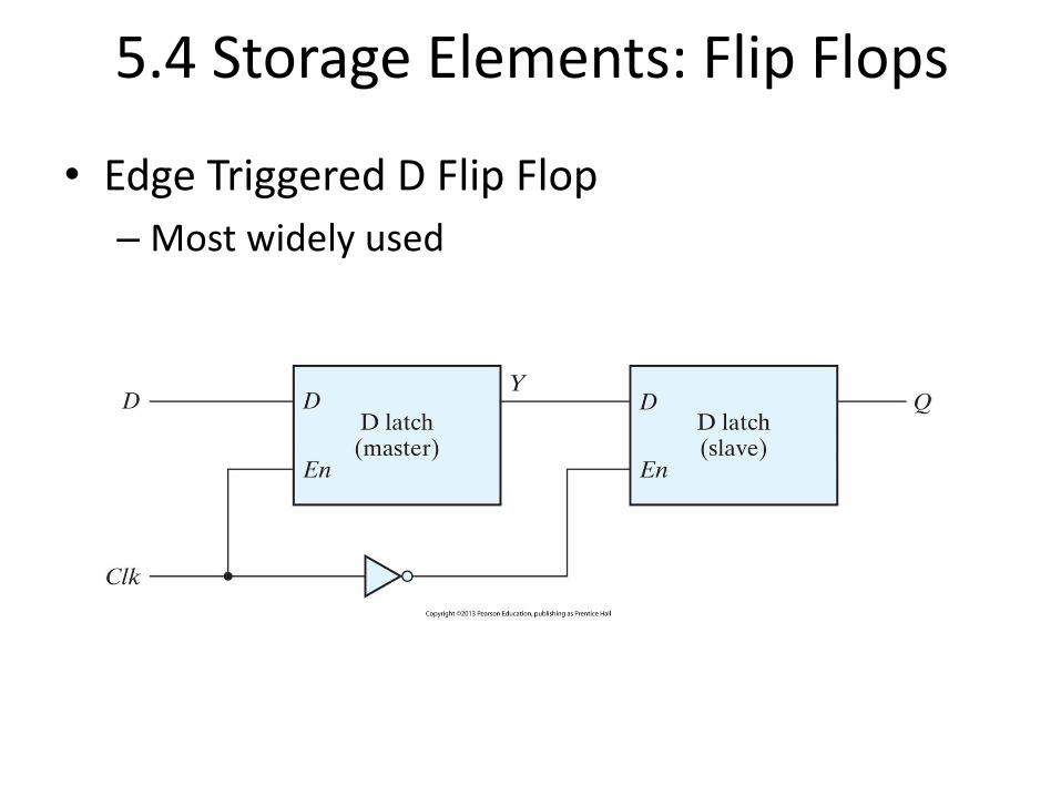
Transmission Gate base D Flip Flop • Previous design are too big for industry applications
– Figure 5.9 Flip Flop uses:
• 8 NANDs (8 * 4 = 32 transistors)
• 3 NOTs (3 * 2 = 6 transistors)
• Transmission gate Flip Flop uses • 4 NOTs (4 * 2 = 8 transistors)
• 4 Transmission Gates (4 * 2 = 8 transistors)
38 transistors
16 transistors

Even Smaller T Gate Design

5.4 Storage Elements: Flip Flops • Characteristic Tables
– A characteristic table defines the logical properties that define its operation in tabular format.
Q(t): present state prior to application of clock edge. Q(t+1): next state after clock edge
– JK next state depends on present state when J,K = 0,0 or 1,1 • Q(t+1) = JQ’ + K’Q
– D next state only depends on D input and is independent of present state. • Q(t+1) = D

5.4 Storage Elements: Flip Flops
• Direct Inputs – Asynchronous set and/or reset inputs that force flip
flop to a particular state independently of the clock. – Used to bring storage elements to know state upon
power up or put system in an initial state • May reset part several times during testing
– Asynchronously assert reset but de-assert synchronously • Want all devices to come out of reset at the same time • If reset released at or near active clock edge, flip flop output
could go metastable
– FPGA flip flops initialize to zero upon programming.

D Flop Flop with set/reset
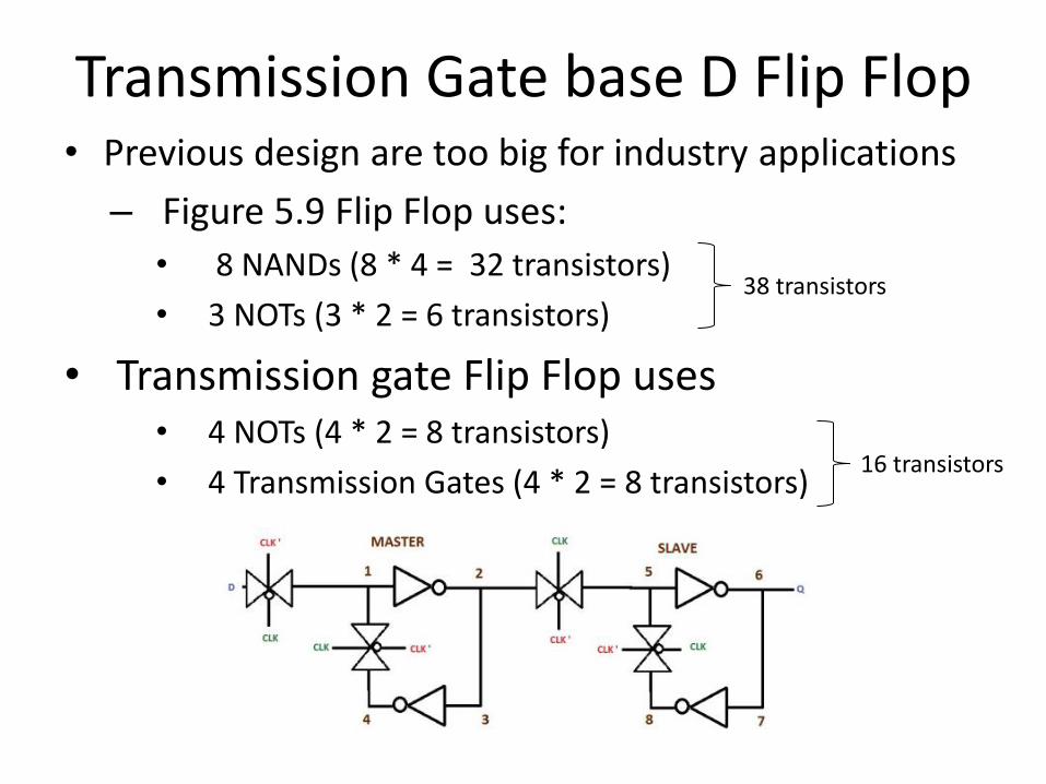
Reset Synchronizer Circuit

Verilog Register Coding module dff_examples (input D, Clk, output Q, Qb); reg DFF_async, DFF_sync; // D Flip Flop Asychronous Reset Example always @(posedge clk or posedge reset) begin if(reset == 1) DFF_async <= 1’b0; else DFF_async <= D; end // Another D Flip Flop Asychronous Reset Example always @(posedge clk, negedge reset) begin if(!reset ) DFF_async <= 1’b0; else DFF_async <= D; end // D Flip Flop Sychronous Reset Example always @(posedge clk ) begin if(reset) DFF_async <= 1’b0; else DFF_async <= D; end

Blocking versus Non-Blocking • Blocking “=“
– Executed sequentially in the order they are listed in the block of statements
• Non-blocking “<=“ – Executes concurrently by evaluating the set of expressions on the right
hand side and then make the left hand side assignments
initial begin @(posedge clk); A = B + 1; // Executes first B = W; // Executes second C = Z || W; // Executes third end
@(posedge clk) begin if(reset) begin A <= 8’h00; B <= 8’hAA; end else begin A <= X && Y; B <= W; end end

Why non-blocking?
• Non-blocking allows modeling of the clock arriving at sequential elements at the same time
@(posedge clk) begin if(reset) begin regA <= 0; regB <= 0; end else begin regA <= X && Y; regB <= regA; end end
clk
X
Y

Blocking versus Non-Blocking
• What about case statement?
– Use blocking assignments to model combinational logic within an always block always @(a or b or sel) begin : mux case (sel) 1'b0: y = a; 1'b1: y = b; default: y = 1'bx; endcase end
Optional name
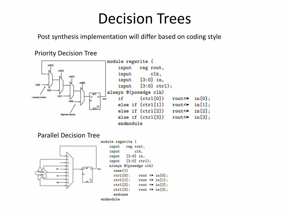
Decision Trees Post synthesis implementation will differ based on coding style
Priority Decision Tree
Parallel Decision Tree

Verilog Compiler Directives
• Compiler directive are preprocessing directives for macro definitions, conditional compilation of code, and file inclusion.
• In lecture 2, we introduce `timescale – Other commonly used directives are (partial list):
`define
`include
`ifdef
`else

Verilog Compiler Directives • A macro is defined using the `define directive:
`define name value
Differs from parameter which must be defines within module boundaries.
• The `include directive allows the inclusion of one file in another: `include " filename “ Note the .vh file extension. This is typically used to indicate files contains compiler directives (`defines, etc.) and not behavioral code.
`define SIZE 32 … reg [`SIZE-1:0] data; `define SZ(num,width) (num)*(width)-1:0 … input [`SZ(32,3)] DeviceData,
`include "Chip.vh"

Verilog Compiler Directives
• Conditional Compilation
– Code may be conditionally compiled using the `ifdef-`else-`endif preprocessor construct
To compile using debug mode with ModelSim:
vlog +define+DEBUG file_name.v
``ifdef DEBUG $display("In debug mode"); `else $display("In normal mode"); `endif
Recommended