Embed Size (px)
Citation preview
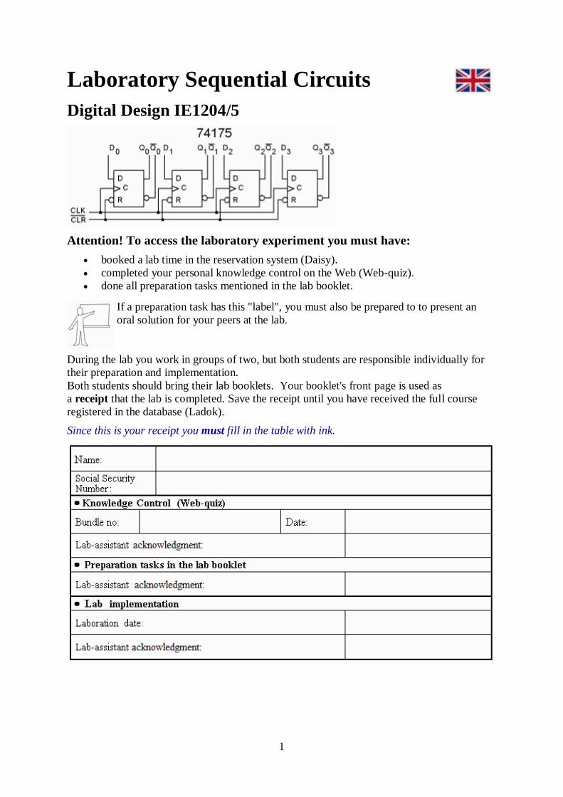
1
Laboratory Sequential Circuits
Digital Design IE1204/5
Attention! To access the laboratory experiment you must have:
booked a lab time in the reservation system (Daisy).
completed your personal knowledge control on the Web (Web-quiz).
done all preparation tasks mentioned in the lab booklet.
If a preparation task has this "label", you must also be prepared to to present an
oral solution for your peers at the lab.
During the lab you work in groups of two, but both students are responsible individually for
their preparation and implementation.
Both students should bring their lab booklets. Your booklet's front page is used as
a receipt that the lab is completed. Save the receipt until you have received the full course
registered in the database (Ladok).
Since this is your receipt you must fill in the table with ink.
2
Introduction
This lab is about designing synchronously clocked sequential circuits. We continue to use
standard CMOS circuits. It's the CMOS technology that has enabled extremely low-power
battery-operated portable devices. CMOS gates only consume power at the clock pulse edges!
(In the lab equipment it is the LEDs that are the big "power consumers").
On the breadboard you will connect and measure some basic sequential circuits like latches
and clocked D flip-flops.
With a systematic method you will construct a state machine, a controlled counter, which you
then test in the laboratory. Other sequential circuits with simple structure, such as feedback
shift registers, can often be examined directly. The task will be to "control" such a sequential
circuit to run through various cycles.
The goal of the lab
Learning how to work with breadboards.
Orienting yourself on latches and clocked flip-flops.
Orienting yourself on programs for electronic simulations.
Showing how the high speed of electronics causes problems, and giving a practical
example of a solution.
Practicing the construction of a state machine using a systematic method.
Practicing measurement techniques, examining a sequential circuit by "forcing" it to
run through different cycles.
Attention! Your lab time may be prior all course elements that may be needed for the lab has
been lectured. You would then have to read the course material for yourself in advance - there
are links to all slides for the lectures and exercises.
3
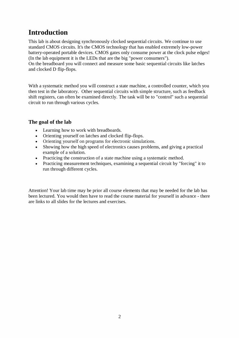
Latch with NOR-gates
A picture of the lab equipment. To the right there is a buffer circuit,
this portion of the lab equipment is not normally used.
Preparation task 1 (done before the lab)
NOR-gates are in the chip 7402, choose two gates from the chip and enter their pin-numbers
in the figures - it will facilitate the connection work at the lab. Try to reason your way to a
truth table for the circuit. (Do not analyze the input combination a=b=0, this you will do at the
lab with a real circuit).
You can also simulate the circuit with LTSpice on your own computer at home in
advance.
Laboratory task 1
Connect the latch on the board using the provided soft cables. The latch
is not a combinational circuit but a sequential circuit. Its output value depends not only on
the input values, but also on the order in which they change.
Operate DIL switches with a screwdriver tip to change the order of their variables to the one
indicated in the table and fill in the output values. Fill in your comments.
- Please note! Do not have the battery plugged in unnecessarily. A weak battery can make
your measurements uncertain even if you wired everything right!
- Attention! You should never "tear down" the basic connections we made in advance on the
board. You should just remove the connections you have made yourself.
4
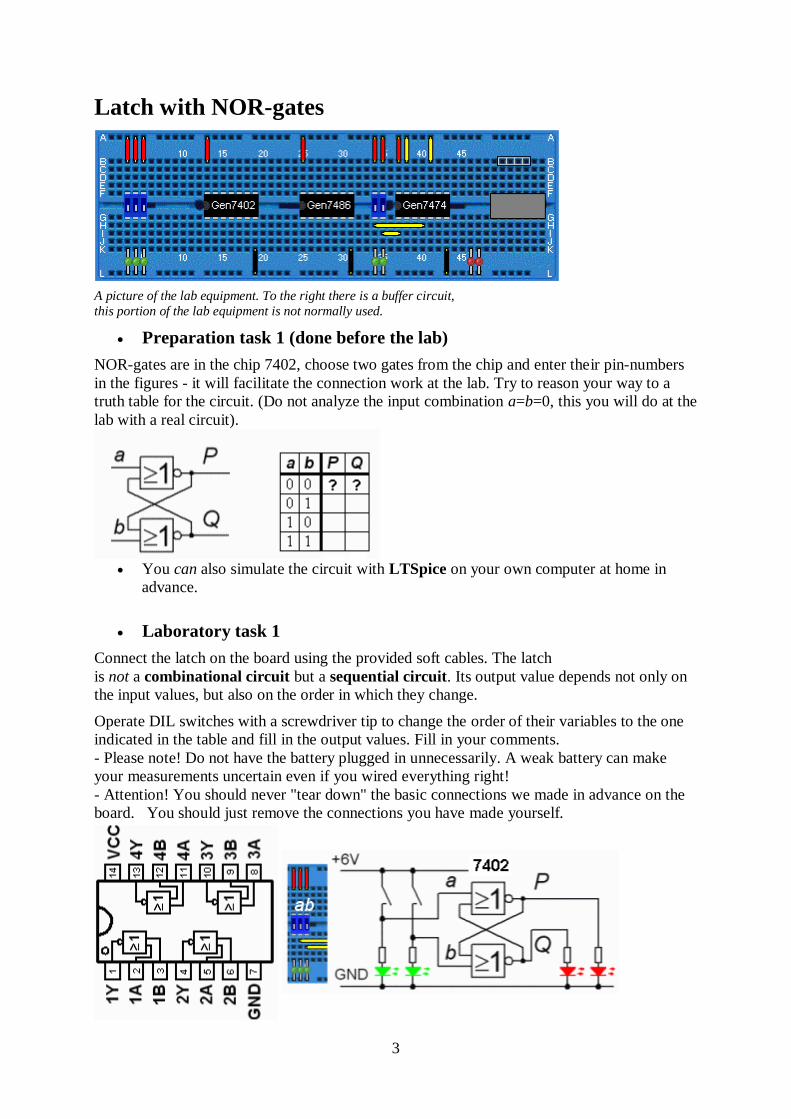
Now identify a, b, P and Q with the variables used in a SR-latch.
Is it possible to say that P and Q are always inverses of each other? Do you have to
prohibit some input combination to make the SR-latch valid?
Preparation task 2 (done before the lab)
Read below about contact bounces and how to avoid them by using a latch.
All mechanical switches exhibit a phenomenon called "contact bounce". It occurs for purely mechanical reasons.
When a switch is pressed, it briefly vibrates at the contact area, which causes the circuit to be closed and opened
many times before the vibration ceased. What makes this a problem is the speed of the electronic circuits, since
contact's vibrations can be confused with (fast) switching. The figure shows that many bounces from "0" to "1"
happen when a switch is pressed.
In the figure, the mechanical switch is connected to a latch. When the switch is turned on, and
starts bouncing, the latch gets preset to "1" and it "remembers" this state. The following
bounces have no impact on the latch. When the switch is then turned off, it resets the latch
directly in a similar way. In this way the output signal of the latch is freed from all
undesirable extra pulses caused by the contact bounce phenomenon.
5
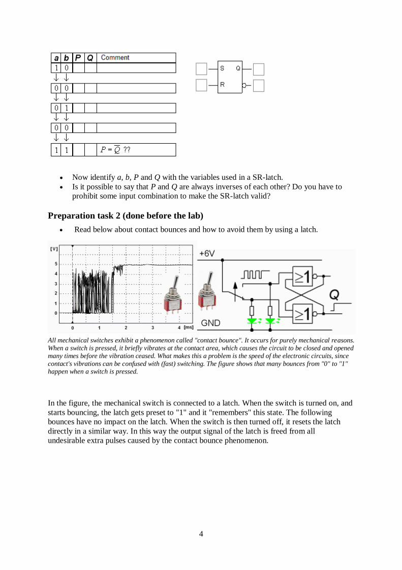
Laboratory task 2
Set the two DIL switches which you used to operate the latch with
into OFF position (so they no longer affect it). Then connect the
mechanical switch as shown. Connect the switch's middle pin to +
6 V and its other two pins to the latch inputs (at the green LEDs).
Contact bounces are so fast that you can not see them directly at
the LEDs. Only during the next experiment, it will be possible to
determine if the contact bounces occur, and check if you can avoid
them with the help of the latch.
Clocked D-flip-flop
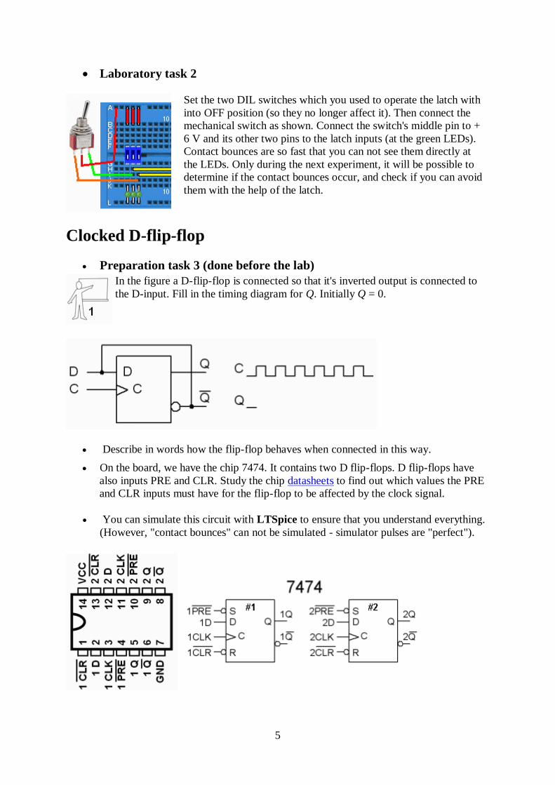
Preparation task 3 (done before the lab)
In the figure a D-flip-flop is connected so that it's inverted output is connected to
the D-input. Fill in the timing diagram for Q. Initially Q = 0.
Describe in words how the flip-flop behaves when connected in this way.
On the board, we have the chip 7474. It contains two D flip-flops. D flip-flops have
also inputs PRE and CLR. Study the chip datasheets to find out which values the PRE
and CLR inputs must have for the flip-flop to be affected by the clock signal.
You can simulate this circuit with LTSpice to ensure that you understand everything.
(However, "contact bounces" can not be simulated - simulator pulses are "perfect").
6
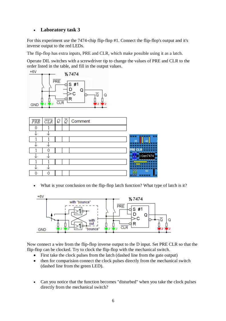
Laboratory task 3
For this experiment use the 7474-chip flip-flop #1. Connect the flip-flop's output and it's
inverse output to the red LEDs.
The flip-flop has extra inputs, PRE and CLR, which make possible using it as a latch.
Operate DIL switches with a screwdriver tip to change the values of PRE and CLR to the
order listed in the table, and fill in the output values.
What is your conclusion on the flip-flop latch function? What type of latch is it?
Now connect a wire from the flip-flop inverse output to the D input. Set PRE CLR so that the
flip-flop can be clocked. Try to clock the flip-flop with the mechanical switch.
First take the clock pulses from the latch (dashed line from the gate output)
then for comparision connect the clock pulses directly from the mechanical switch
(dashed line from the green LED).
Can you notice that the function becomes "disturbed" when you take the clock pulses
directly from the mechanical switch?
7
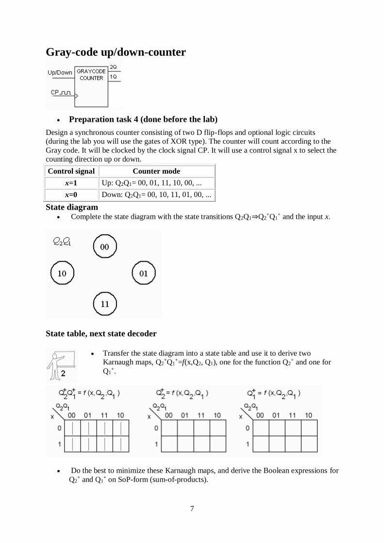
Gray-code up/down-counter
Preparation task 4 (done before the lab)
Design a synchronous counter consisting of two D flip-flops and optional logic circuits
(during the lab you will use the gates of XOR type). The counter will count according to the
Gray code. It will be clocked by the clock signal CP. It will use a control signal x to select the
counting direction up or down.
Control signal Counter mode
x=1 Up: Q2Q1= 00, 01, 11, 10, 00, ...
x=0 Down: Q2Q1= 00, 10, 11, 01, 00, ...
State diagram Complete the state diagram with the state transitions Q2Q1⇒Q2
+Q1+ and the input x.
State table, next state decoder
Transfer the state diagram into a state table and use it to derive two
Karnaugh maps, Q2+Q1
+=f(x,Q2, Q1), one for the function Q2+ and one for
Q1+.
Do the best to minimize these Karnaugh maps, and derive the Boolean expressions for
Q2+ and Q1
+ on SoP-form (sum-of-products).
8
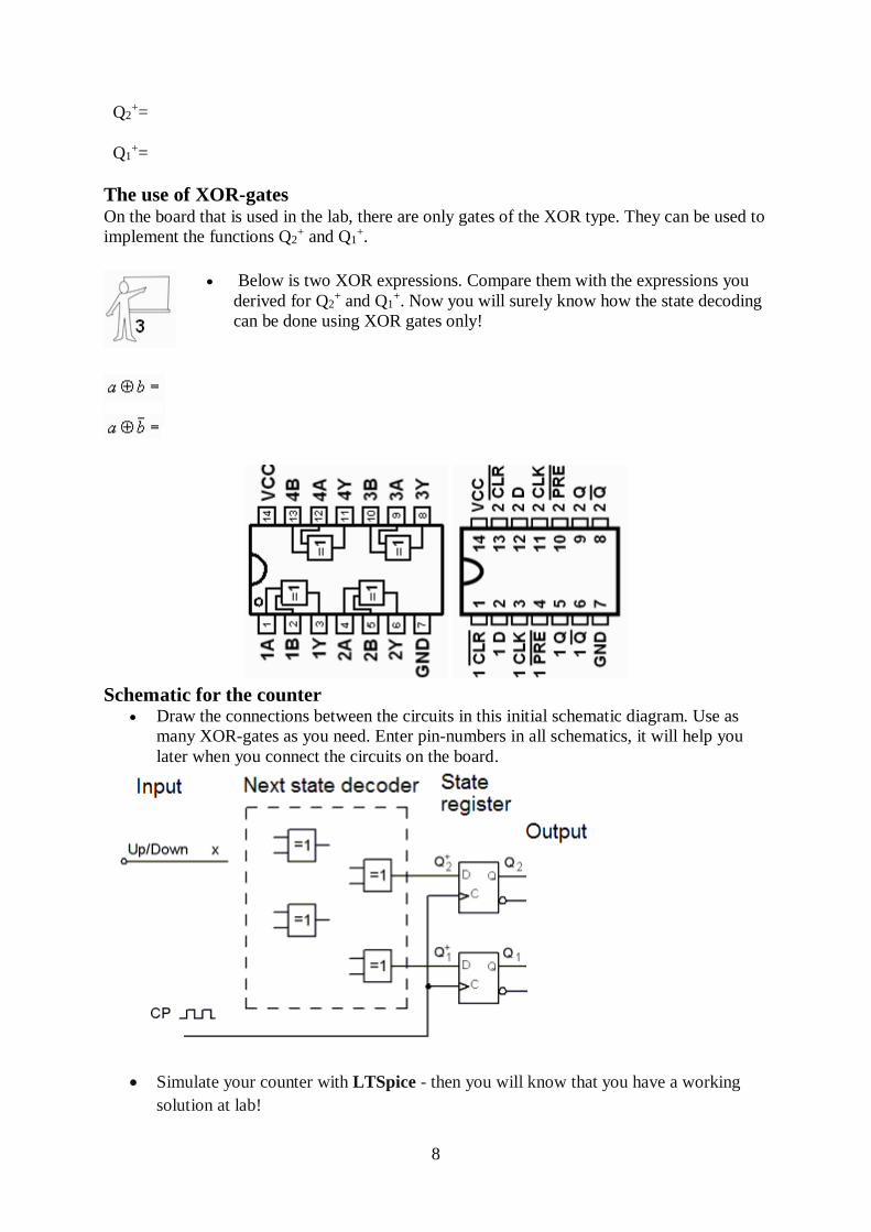
Q2+=
Q1+=
The use of XOR-gates On the board that is used in the lab, there are only gates of the XOR type. They can be used to
implement the functions Q2+ and Q1
+.
Below is two XOR expressions. Compare them with the expressions you
derived for Q2+ and Q1
+. Now you will surely know how the state decoding
can be done using XOR gates only!
Schematic for the counter Draw the connections between the circuits in this initial schematic diagram. Use as
many XOR-gates as you need. Enter pin-numbers in all schematics, it will help you
later when you connect the circuits on the board.
Simulate your counter with LTSpice - then you will know that you have a working
solution at lab!
9
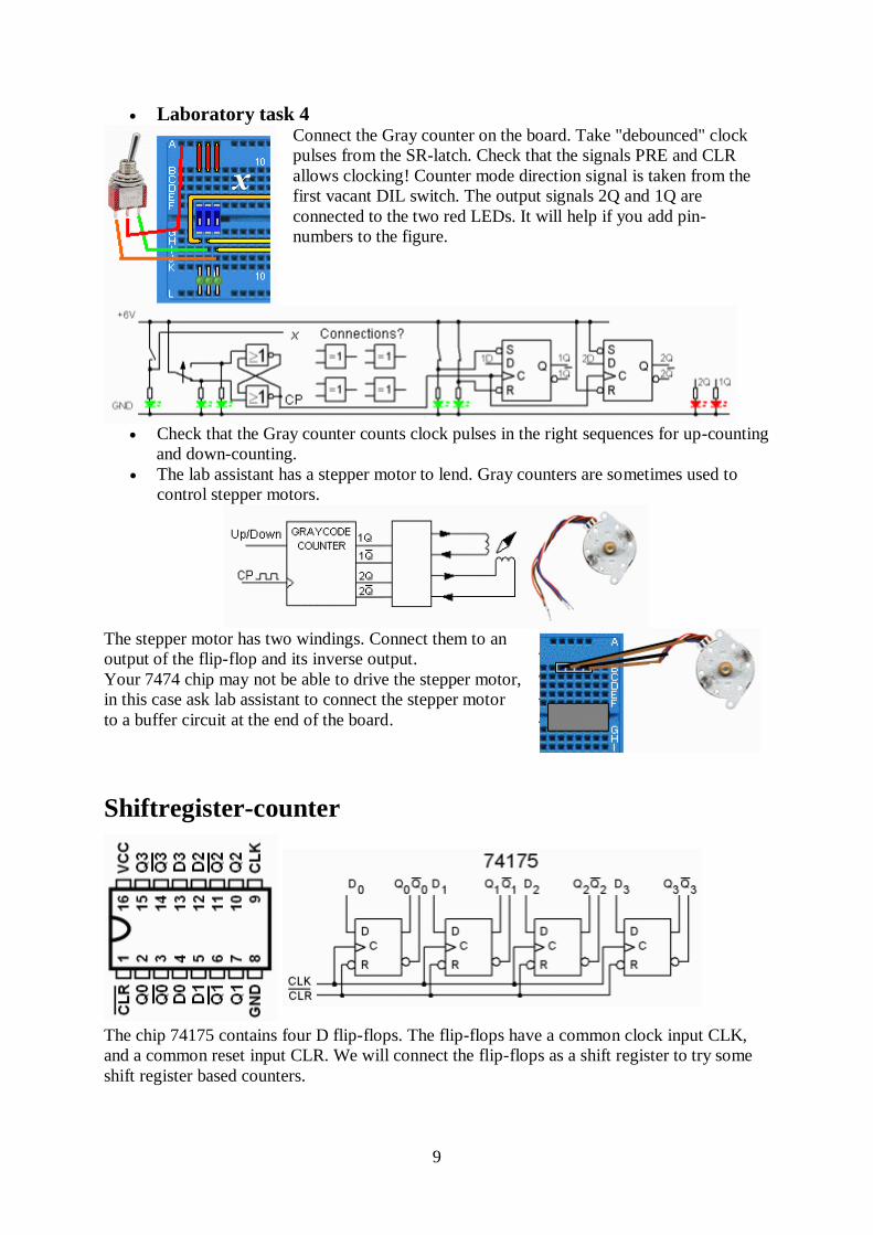
Laboratory task 4
Connect the Gray counter on the board. Take "debounced" clock
pulses from the SR-latch. Check that the signals PRE and CLR
allows clocking! Counter mode direction signal is taken from the
first vacant DIL switch. The output signals 2Q and 1Q are
connected to the two red LEDs. It will help if you add pin-
numbers to the figure.
Check that the Gray counter counts clock pulses in the right sequences for up-counting
and down-counting.
The lab assistant has a stepper motor to lend. Gray counters are sometimes used to
control stepper motors.
The stepper motor has two windings. Connect them to an
output of the flip-flop and its inverse output.
Your 7474 chip may not be able to drive the stepper motor,
in this case ask lab assistant to connect the stepper motor
to a buffer circuit at the end of the board.
Shiftregister-counter
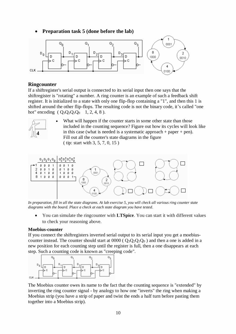
The chip 74175 contains four D flip-flops. The flip-flops have a common clock input CLK,
and a common reset input CLR. We will connect the flip-flops as a shift register to try some
shift register based counters.
10
Preparation task 5 (done before the lab)
Ringcounter If a shiftregister's serial output is connected to its serial input then one says that the
shiftregister is "rotating" a number. A ring counter is an example of such a feedback shift
register. It is initialized to a state with only one flip-flop containing a "1", and then this 1 is
shifted around the other flip-flops. The resulting code is not the binary code, it’s called "one
hot" encoding ( Q3Q2Q1Q0 1, 2, 4, 8 ).
What will happen if the counter starts in some other state than those
included in the counting sequence? Figure out how its cycles will look like
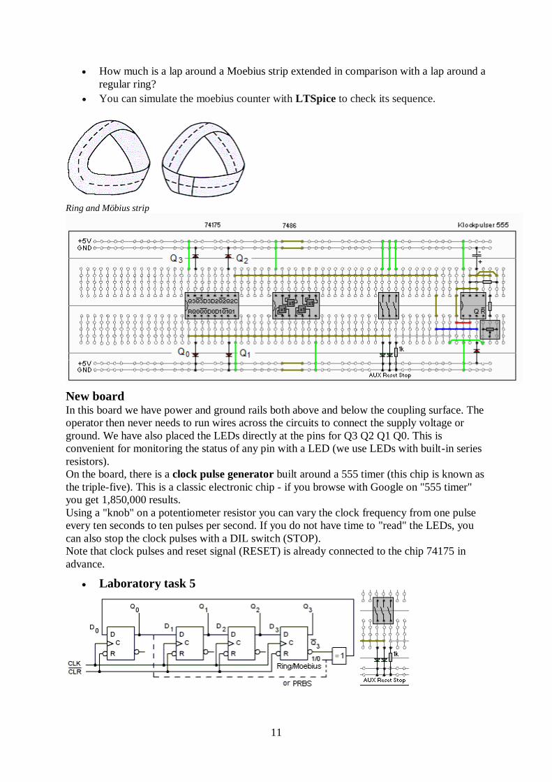
in this case (what is needed is a systematic approach + paper + pen).
Fill out all the counter's state diagrams in the figure
( tip: start with 3, 5, 7, 0, 15 )
In preparation, fill in all the state diagrams. At lab exercise 5, you will check all various ring counter state
diagrams with the board. Place a check at each state diagram you have tested.
You can simulate the ringcounter with LTSpice. You can start it with different values
to check your reasoning above.
Moebius-counter
If you connect the shiftregisters inverted serial output to its serial input you get a moebius-
counter instead. The counter should start at 0000 ( Q3Q2Q1Q0 ) and then a one is added in a
new position for each counting step until the register is full, then a one disappears at each
step. Such a counting code is known as "creeping code".
The Moebius counter owes its name to the fact that the counting sequence is "extended" by
inverting the ring counter signal - by analogy to how one "inverts" the ring when making a
Moebius strip (you have a strip of paper and twist the ends a half turn before pasting them
together into a Moebius strip).
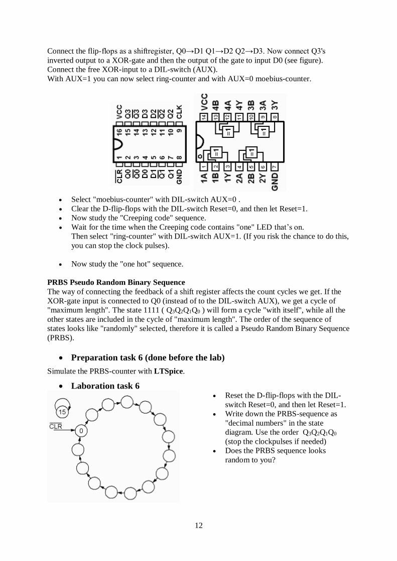
11
How much is a lap around a Moebius strip extended in comparison with a lap around a
regular ring?
You can simulate the moebius counter with LTSpice to check its sequence.
Ring and Möbius strip
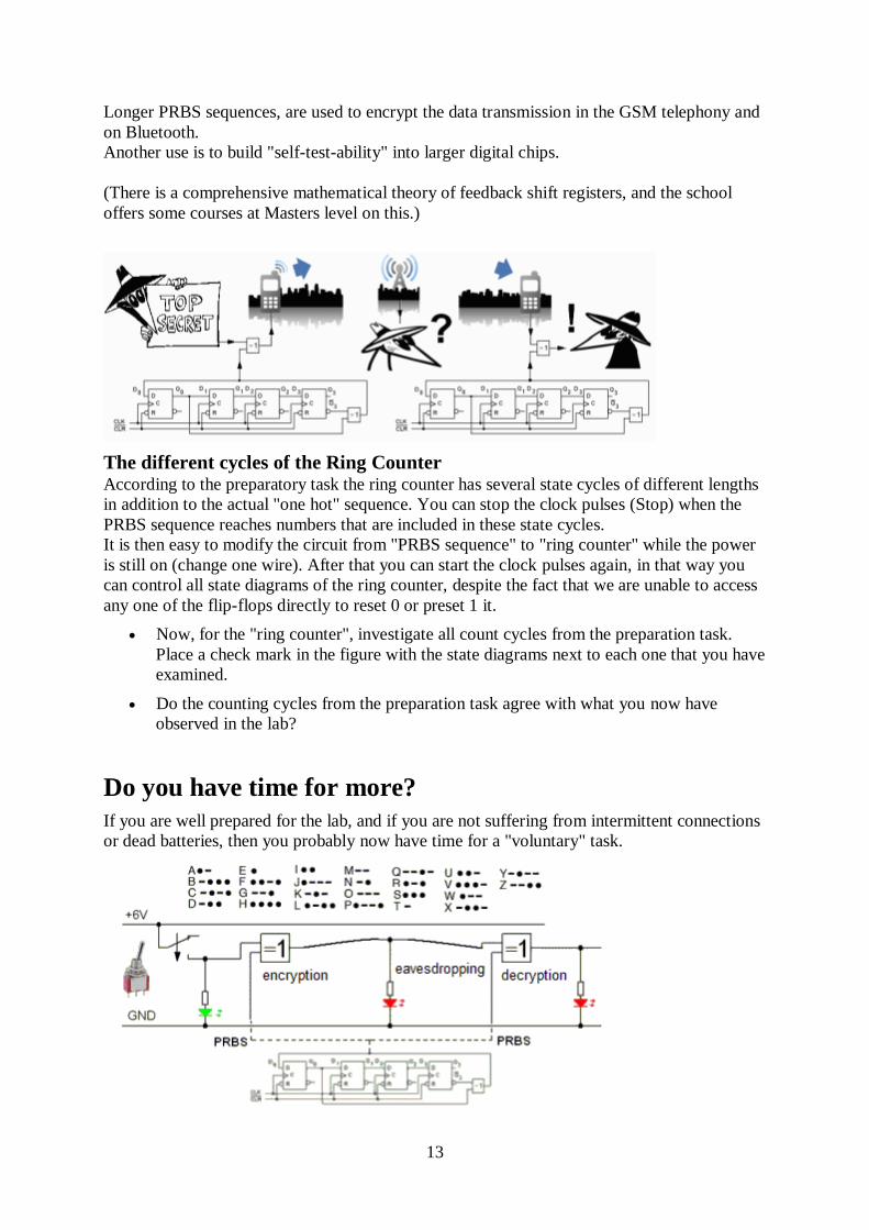
New board In this board we have power and ground rails both above and below the coupling surface. The
operator then never needs to run wires across the circuits to connect the supply voltage or
ground. We have also placed the LEDs directly at the pins for Q3 Q2 Q1 Q0. This is
convenient for monitoring the status of any pin with a LED (we use LEDs with built-in series
resistors).
On the board, there is a clock pulse generator built around a 555 timer (this chip is known as
the triple-five). This is a classic electronic chip - if you browse with Google on "555 timer"
you get 1,850,000 results.
Using a "knob" on a potentiometer resistor you can vary the clock frequency from one pulse
every ten seconds to ten pulses per second. If you do not have time to "read" the LEDs, you
can also stop the clock pulses with a DIL switch (STOP).
Note that clock pulses and reset signal (RESET) is already connected to the chip 74175 in
advance.
Laboratory task 5
12
Connect the flip-flops as a shiftregister, Q0→D1 Q1→D2 Q2→D3. Now connect Q3's
inverted output to a XOR-gate and then the output of the gate to input D0 (see figure).
Connect the free XOR-input to a DIL-switch (AUX).
With AUX=1 you can now select ring-counter and with AUX=0 moebius-counter.
Select "moebius-counter" with DIL-switch AUX=0 .
Clear the D-flip-flops with the DIL-switch Reset=0, and then let Reset=1.
Now study the "Creeping code" sequence.
Wait for the time when the Creeping code contains "one" LED that’s on.
Then select "ring-counter" with DIL-switch AUX=1. (If you risk the chance to do this,
you can stop the clock pulses).
Now study the "one hot" sequence.
PRBS Pseudo Random Binary Sequence
The way of connecting the feedback of a shift register affects the count cycles we get. If the
XOR-gate input is connected to Q0 (instead of to the DIL-switch AUX), we get a cycle of
"maximum length". The state 1111 ( Q3Q2Q1Q0 ) will form a cycle "with itself", while all the
other states are included in the cycle of "maximum length". The order of the sequence of
states looks like "randomly" selected, therefore it is called a Pseudo Random Binary Sequence
(PRBS).
Preparation task 6 (done before the lab)
Simulate the PRBS-counter with LTSpice.
Laboration task 6
Reset the D-flip-flops with the DIL-
switch Reset=0, and then let Reset=1.
Write down the PRBS-sequence as
"decimal numbers" in the state
diagram. Use the order Q3Q2Q1Q0
(stop the clockpulses if needed)
Does the PRBS sequence looks
random to you?
13
Longer PRBS sequences, are used to encrypt the data transmission in the GSM telephony and
on Bluetooth.
Another use is to build "self-test-ability" into larger digital chips.
(There is a comprehensive mathematical theory of feedback shift registers, and the school
offers some courses at Masters level on this.)
The different cycles of the Ring Counter According to the preparatory task the ring counter has several state cycles of different lengths
in addition to the actual "one hot" sequence. You can stop the clock pulses (Stop) when the
PRBS sequence reaches numbers that are included in these state cycles.
It is then easy to modify the circuit from "PRBS sequence" to "ring counter" while the power
is still on (change one wire). After that you can start the clock pulses again, in that way you
can control all state diagrams of the ring counter, despite the fact that we are unable to access
any one of the flip-flops directly to reset 0 or preset 1 it.
Now, for the "ring counter", investigate all count cycles from the preparation task.
Place a check mark in the figure with the state diagrams next to each one that you have
examined.
Do the counting cycles from the preparation task agree with what you now have
observed in the lab?
Do you have time for more?
If you are well prepared for the lab, and if you are not suffering from intermittent connections
or dead batteries, then you probably now have time for a "voluntary" task.
14
Leave PRBS-generator connected. The chip 7486 has three unused XOR-gates left, use two of
them. "Borrow" the mechanical switch and a green and two red LEDs from the other lab
board. (Do not forget to put them back again when you are finished).
Connect the circuit as shown in the figure. It is an encrypted data transfer. Transmitter and
receiver mixes the data signal synchronized with the PRBS signal.
We "cheat" when it comes to the synchronization problem by simply allowing the transmitter
and receiver to use the same PRBS-signal.
Send a message with Morse code and make sure that the recipient can read the message -
while anyone trying to eavesdrop on the communication has no chance!
Good luck!
When you are finished. Remove all the connections that you have made, but no
others, and clean the lab desk.
Bill of materials
The "bill of material" for the lab equipment, could be helpful if you ever would need to use
simple logic functions yourself.
Breadboard GL-12F ELFA 48-427-04
Battery contact ELFA 42-043-01
Battery Holder 6V ELFA 4xR6 ELFA 69-506-61
DIL-switch 3P ELFA 35-395-25
DIL-switch 2P ELFA 35-395-17
Lightdiode with series resistor 5V green ELFA 75-014-99
Lightdiode with series resistor 5V red ELFA 75-012-59
Rocker switch on-(on) 1P ELFA 35-305-24
NOR-gates 74HC02 ELFA 73-501-19
XOR-gates 74HC86 ELFA 73-515-13
4D-flip-flops 74HC175 ELFA 73-529-17
2D-flip-flops CD74AC74E (måste vara AC) ELFA 73-621-24
Electronics circuit 555 ELFA 73-042-65
Trimming Potentiometer 500 kO with adjustment knob ELFA 64-635-25
© William Sandqvist [email protected]