Investigation of
Resonant-Cavity-Enhanced
Mercury Cadmium Telluride
Infrared Detectors
By
Justin G. A. Wehner BE(Hons) BSc
This thesis is presented for the degree of
Doctor of Philosophy of
The University of Western Australia
School of Electrical, Electronic and Computer Engineering
The University of Western Australia
2007

Declaration of Published Work Appearing in Thesis.
This thesis contains published work and/or work prepared for publication, some
of which has been co-authored. The bibliographic details of the works and where
they appear in the thesis are set out in appendices E and F, respectively. The details of
contribution of each paper are outlined in appendix E.
Signature:............................. (Candidate)
Justin G.A. Wehner
Signature:............................. (Supervisor)
A/Prof. J.M. Dell
Signature:............................. (Supervisor)
Prof. L. Faraone

Justin Wehner
3/158 Broadway
Nedlands, Western Australia
Australia 6009
2007
Executive Dean,
Faculty of Engineering,
Computing and Mathematics,
The University of Western Australia, Crawley,
Western Australia, 6009
Australia
Dear Sir,
I am pleased to present this thesis entitled Investigation of Resonant-Cavity-
Enhanced Mercury Cadmium Telluride Infrared Detectors as required for a Doctor of
Philosophy Degree.
Yours sincerely,
Justin G. A. Wehner
i

ii
Abstract
Infrared (IR) detectors have many applications, from homeland security and defense, to
medical imaging, to environmental monitoring, to astronomy, etc. Increasingly, the wave-
length dependence of the IR radiation is becoming important in many applications, not
just the total intensity of infrared radiation. There are many types of infrared detectors
that can be broadly categorized as either photon detectors (narrow band-gap materials
or quantum structures that provide the necessary energy transitions to generate free car-
riers) or thermal detectors. Photon detectors generally provide the highest sensitivity,
however the small transition energy of the detector also means cooling is required to limit
the noise due to intrinsic thermal generation. This thesis is concerned with the tech-
nique of resonant-cavity-enhancement of detectors, which is the process of placing the
detector within an optically resonant cavity. Resonant-cavity-enhanced detectors have
many favourable properties including a reduced detector volume, which allows improved
operating temperature, or an improved signal to noise ratio (or some balance between the
two), along with a narrow spectral bandwidth.
This thesis uses the HgCdTe material system as a vehicle for investigation of resonant-
cavity-enhanced (RCE) detectors. IR detectors based on HgCdTe currently give the
highest sensitivity and RCE devices based on HgCdTe represent an excellent candidates
for improved (higher) operating temperature devices or narrow optical bandwidth de-
vices. Modelling of RCE device performance is performed to illustrate the benefits of
resonant-cavity-enhancement. Growth of RCE detectors by molecular beam epitaxy is
also investigated. Firstly, the design and growth of staggered HgCdTe dielectric mirrors
on which absorber layers can be grown is investigated. This is followed by design and
growth of complete RCE detectors, proving that RCE detectors for infrared applications
can be realised.
Modelling of RCE detectors indicates that decreasing the thickness of a photoconductive
detector by d will result in an increase in the detectivity which corresponds to√d.
For photovoltaic detectors, reducing the detector thickness from 10 µm to 100 nm thick
will increase the device zero-bias dynamic resistance, which is directly proportional to
detectivity, by approximately 2 orders of magnitude. These gains can result in a detector
that is able to operate at background limited performance at a temperature of 240K for
a 30 field of view (f/# = 1.86), which is well above the background limited temperature
of current generation detectors.
Mirror technology for fabricating resonant-cavity-enhanced detectors was investigated,
with the Hg(1−x)Cd(x)Te/CdTe material system used to provide the surface on which the
absorber layer is to be grown. Staggered dielectric mirrors are used to broaden the mirror
response of Hg(1−x)Cd(x)Te/CdTe mirrors from a few hundred nanometers for a quarter-
wave-stack to approximately 1 µm for a 17 layer mirror. The reflectivity of such a mirror
is reduced from ≈ 0.95 to ≈ 0.7. Mirror stacks were grown by molecular beam epitaxy and
exhibit strong reflectivity. In order to obtain good agreement between modelled response
iii
and measured mirror response, the refractive index of the CdTe layers had to be reduced
significantly. This is shown to be due to the presence of voids within the CdTe, with a
volume concentration of ≈ 10%.
The mirror layers were also investigated after annealing using conditions similar to those
required for preparation of MBE grown HgCdTe layers for device fabrication. The mirrors
were found to remain reflective after a typical annealing cycle of 20 hours at 250C in a
Hg atmosphere, with minimal degradation. The annealed layers were investigated using
secondary-ion mass-spectroscopy, to measure composition as a function of depth. The
profiles illustrated that there was minimal grading between the CdTe and Hg(1−x)Cd(x)Te
layers even after extended annealing, which for the CdTe on Hg(1−x)Cd(x)Te layers was
in agreement with interdiffusion modelling data. Grading of Hg(1−x)Cd(x)Te layers on
CdTe was greater than expected from model data, possibly due to the presence of voids
in the CdTe layer increasing the diffusion coefficient of Hg in CdTe.
Resonant-cavity-enhanced detector structures based on photoconductors were designed,
resulting in a proof-of-concept structure that was subsequently grown by molecular beam
epitaxy (MBE). A sample which was annealed in-situ in the MBE chamber at the growth
temperature (185C) for 30 minutes under a Hg flux to reduce the Hg vacancy concen-
tration, exhibited resonant-cavity performance with peak responsivity of 1×10⁴ V/W for
a 75 nm thick 80 µm × 500 µm photoconductor at 80K, with a reasonable fit to model
data. Noise measurements were inconclusive, but a worst-case detectivity was calculated
to be 3.09×109 cm Hz1/2 W−1, while detectivity at 200K was calculated to be 4.48×10⁸
cm Hz1/2 W−1. Varying the temperature resulted in a shifting cut-off, in agreement with
model data. The minority carrier lifetime extracted for this sample was 14 ns. Adding
a Ge/SiO mirror to complete the resonant cavity resulted in a reduction of response at
shorter wavelengths, in agreement with model results.
Responsivity of another sample annealed for 20 hours at 250C in a Hg atmosphere
(ex-situ) also shows resonant performance, but indicates significant shunting due the
mirror layers. There is good agreement with model data, and the peak responsivity
due to the absorber layer is 9.5×10³ V/W for a 100 µm × 100 µm photoconductor at
80K. An effective lifetime of 50.4 ns is extracted for this responsivity measurement. The
responsivity was measured as a function of varying field, and sweepout was observed for
bias fields greater than 50 V/cm. The effective lifetime extracted from this measurement
was 224 ns, but is an over estimate.
Photodiodes were also fabricated by annealing p-type Hg(1−x)Cd(x)Te for 10 hours at
250C in vacuum and type converting in a CH4/H2 reactive ion etch plasma process
to form the n-p junction. There is some degradation to the mirror structure due to
the anneal in vacuum, but a clear region of high reflection is observed. Measurements
of current-voltage characteristics at various temperatures show diode-like characteristics
with a peak R0 of 10 GΩ measured at 80K (corresponding to an R0A of approximately
104 Ωcm2. There was significant signal from the mirror layers, however only negligible
signal from the absorber layer, and no conclusive resonant peaks.
iv
Table of contents
Abstract iii
Table of Contents v
Acknowledgments xi
List of Acronyms xiii
List of Symbols xv
1 Introduction 19
1.1 Infrared Radiation . . . . . . . . . . . . . . . . . . . . . . . . . . . . . . . 19
1.1.1 Blackbody Radiation . . . . . . . . . . . . . . . . . . . . . . . . . . 20
1.2 Applications of Infrared Sensing . . . . . . . . . . . . . . . . . . . . . . . . 22
1.2.1 Infrared Sensing Devices . . . . . . . . . . . . . . . . . . . . . . . . 24
1.2.2 Broadband Infrared Photon Detectors . . . . . . . . . . . . . . . . 25
1.2.3 Two-colour Detectors . . . . . . . . . . . . . . . . . . . . . . . . . 25
1.2.4 Multi- and Hyper-spectral Sensors . . . . . . . . . . . . . . . . . . 26
1.2.5 Methods for Improving Sensors . . . . . . . . . . . . . . . . . . . . 28
1.3 Thesis Objectives . . . . . . . . . . . . . . . . . . . . . . . . . . . . . . . . 29
1.3.1 Thesis Structure . . . . . . . . . . . . . . . . . . . . . . . . . . . . 29
v
2 Infrared Detectors 31
2.1 Introduction . . . . . . . . . . . . . . . . . . . . . . . . . . . . . . . . . . . 31
2.2 Detector Types . . . . . . . . . . . . . . . . . . . . . . . . . . . . . . . . . 31
2.2.1 Thermal Detectors . . . . . . . . . . . . . . . . . . . . . . . . . . . 31
2.2.2 Photon Detectors . . . . . . . . . . . . . . . . . . . . . . . . . . . . 32
2.3 Material/Structures for Photon Detectors . . . . . . . . . . . . . . . . . . 36
2.3.1 Bulk Material . . . . . . . . . . . . . . . . . . . . . . . . . . . . . . 36
2.3.2 Band-gap Engineered Structures . . . . . . . . . . . . . . . . . . . 37
2.4 Material Properties . . . . . . . . . . . . . . . . . . . . . . . . . . . . . . . 38
2.4.1 Absorption Co-efficient . . . . . . . . . . . . . . . . . . . . . . . . 38
2.4.2 Lifetime . . . . . . . . . . . . . . . . . . . . . . . . . . . . . . . . . 40
2.4.3 This Work . . . . . . . . . . . . . . . . . . . . . . . . . . . . . . . . 45
2.5 Metrics and Detector Figures of Merit . . . . . . . . . . . . . . . . . . . . 47
2.5.1 Quantum Efficiency . . . . . . . . . . . . . . . . . . . . . . . . . . 47
2.5.2 Resistance . . . . . . . . . . . . . . . . . . . . . . . . . . . . . . . . 48
2.5.3 Depletion Region Width . . . . . . . . . . . . . . . . . . . . . . . . 51
2.5.4 Responsivity . . . . . . . . . . . . . . . . . . . . . . . . . . . . . . 52
2.5.5 Dark Currents and Noise . . . . . . . . . . . . . . . . . . . . . . . 52
2.5.6 Noise Equivalent Power and Detectivity . . . . . . . . . . . . . . . 55
2.5.7 Specific Detectivity . . . . . . . . . . . . . . . . . . . . . . . . . . . 56
2.6 Experimental Techniques . . . . . . . . . . . . . . . . . . . . . . . . . . . 57
2.6.1 Material Characterisation . . . . . . . . . . . . . . . . . . . . . . . 57
2.6.2 Device Characterisation . . . . . . . . . . . . . . . . . . . . . . . . 58
3 Theory of Resonant-cavity-enhanced Detectors 61
3.1 Introduction . . . . . . . . . . . . . . . . . . . . . . . . . . . . . . . . . . . 61
3.2 Methods of Improvement . . . . . . . . . . . . . . . . . . . . . . . . . . . 61
3.2.1 Heterostructure Devices . . . . . . . . . . . . . . . . . . . . . . . . 62
3.2.2 Multi-junction Devices . . . . . . . . . . . . . . . . . . . . . . . . . 62
3.2.3 Resonant-cavity-enhanced Devices . . . . . . . . . . . . . . . . . . 63
vi
3.3 Fabry-Perot Cavities . . . . . . . . . . . . . . . . . . . . . . . . . . . . . . 63
3.3.1 Figures of Merit . . . . . . . . . . . . . . . . . . . . . . . . . . . . 65
3.3.2 Energy Density . . . . . . . . . . . . . . . . . . . . . . . . . . . . . 66
3.3.3 Fabry-Perot Cavities with Absorption . . . . . . . . . . . . . . . . 67
3.3.4 Effect of Mirror Phase . . . . . . . . . . . . . . . . . . . . . . . . . 72
3.4 Examples of RCE Devices . . . . . . . . . . . . . . . . . . . . . . . . . . . 73
3.5 Advantages . . . . . . . . . . . . . . . . . . . . . . . . . . . . . . . . . . . 73
3.5.1 Speed . . . . . . . . . . . . . . . . . . . . . . . . . . . . . . . . . . 73
3.5.2 Improved Quantum Efficiency . . . . . . . . . . . . . . . . . . . . . 74
3.5.3 Reduced Volume . . . . . . . . . . . . . . . . . . . . . . . . . . . . 75
3.6 Technologies for Growing RCE Structures . . . . . . . . . . . . . . . . . . 80
4 Staggered Dielectric Mirrors 83
4.1 Introduction . . . . . . . . . . . . . . . . . . . . . . . . . . . . . . . . . . . 83
4.2 Modelling of Mirrors . . . . . . . . . . . . . . . . . . . . . . . . . . . . . . 84
4.2.1 Quarter-wave Stack . . . . . . . . . . . . . . . . . . . . . . . . . . 84
4.2.2 Staggered Dielectric Mirrors . . . . . . . . . . . . . . . . . . . . . . 85
4.2.3 Phase Variations . . . . . . . . . . . . . . . . . . . . . . . . . . . . 88
4.2.4 Final Mirror Design . . . . . . . . . . . . . . . . . . . . . . . . . . 90
4.3 HgCdTe/CdTe Mirror Growth . . . . . . . . . . . . . . . . . . . . . . . . 92
4.3.1 Substrate Preparation . . . . . . . . . . . . . . . . . . . . . . . . . 92
4.3.2 Growth . . . . . . . . . . . . . . . . . . . . . . . . . . . . . . . . . 92
4.3.3 Annealing . . . . . . . . . . . . . . . . . . . . . . . . . . . . . . . . 95
4.3.4 Interdiffusion Modelling . . . . . . . . . . . . . . . . . . . . . . . . 96
4.4 Experimental Results . . . . . . . . . . . . . . . . . . . . . . . . . . . . . . 100
4.4.1 Mirror-MCT75 . . . . . . . . . . . . . . . . . . . . . . . . . . . . . 100
4.4.2 Annealing . . . . . . . . . . . . . . . . . . . . . . . . . . . . . . . . 102
4.4.3 Refractive Index . . . . . . . . . . . . . . . . . . . . . . . . . . . . 106
4.5 Conclusions . . . . . . . . . . . . . . . . . . . . . . . . . . . . . . . . . . . 115
vii
5 Realisation of Resonant-cavity-enhanced Detectors 117
5.1 Introduction . . . . . . . . . . . . . . . . . . . . . . . . . . . . . . . . . . . 117
5.2 RCE Detector Design and Modelling . . . . . . . . . . . . . . . . . . . . . 117
5.2.1 RCE Design . . . . . . . . . . . . . . . . . . . . . . . . . . . . . . . 117
5.2.2 Responsivity . . . . . . . . . . . . . . . . . . . . . . . . . . . . . . 126
5.3 MBE Growth . . . . . . . . . . . . . . . . . . . . . . . . . . . . . . . . . . 127
5.4 Photoconductor Fabrication . . . . . . . . . . . . . . . . . . . . . . . . . . 129
5.4.1 Fabrication . . . . . . . . . . . . . . . . . . . . . . . . . . . . . . . 129
5.4.2 Device Layout . . . . . . . . . . . . . . . . . . . . . . . . . . . . . 130
5.5 Experimental Results . . . . . . . . . . . . . . . . . . . . . . . . . . . . . . 130
5.5.1 MCT-79 - Without Ge/SiO Mirror . . . . . . . . . . . . . . . . . . 136
5.5.2 MCT-79 - Complete Structure . . . . . . . . . . . . . . . . . . . . 144
5.5.3 Noise Measurements - MCT-79 . . . . . . . . . . . . . . . . . . . . 147
5.5.4 Contact Issues - MCT-79 . . . . . . . . . . . . . . . . . . . . . . . 150
5.5.5 MCT-92 - Without Ge/SiO Mirror . . . . . . . . . . . . . . . . . . 150
5.5.6 Contact Issues - MCT-92 . . . . . . . . . . . . . . . . . . . . . . . 155
5.6 Proceeding on to Photovoltaic Detectors . . . . . . . . . . . . . . . . . . . 156
5.6.1 Processing - MCT-95 . . . . . . . . . . . . . . . . . . . . . . . . . . 157
5.6.2 Results - MCT-95 . . . . . . . . . . . . . . . . . . . . . . . . . . . 159
5.7 Conclusions . . . . . . . . . . . . . . . . . . . . . . . . . . . . . . . . . . . 162
6 Summary and Conclusions 165
6.1 Thesis Objectives . . . . . . . . . . . . . . . . . . . . . . . . . . . . . . . . 165
6.2 Outcomes . . . . . . . . . . . . . . . . . . . . . . . . . . . . . . . . . . . . 165
6.3 Original Results . . . . . . . . . . . . . . . . . . . . . . . . . . . . . . . . . 167
6.4 Conclusions . . . . . . . . . . . . . . . . . . . . . . . . . . . . . . . . . . . 169
6.5 Future Work . . . . . . . . . . . . . . . . . . . . . . . . . . . . . . . . . . 169
References 169
viii
Appendices
A Properties of Mercury Cadmium Telluride 185
A.1 Introduction . . . . . . . . . . . . . . . . . . . . . . . . . . . . . . . . . . . 185
A.2 Crystal Structure . . . . . . . . . . . . . . . . . . . . . . . . . . . . . . . . 185
A.3 Energy Band-gap . . . . . . . . . . . . . . . . . . . . . . . . . . . . . . . . 185
A.4 Intrinsic Carrier Concentration . . . . . . . . . . . . . . . . . . . . . . . . 186
A.4.1 Majority and Minority Carrier Concentration . . . . . . . . . . . . 187
A.5 Effective Mass . . . . . . . . . . . . . . . . . . . . . . . . . . . . . . . . . . 188
A.6 Mobility . . . . . . . . . . . . . . . . . . . . . . . . . . . . . . . . . . . . . 188
A.7 Carrier Lifetimes . . . . . . . . . . . . . . . . . . . . . . . . . . . . . . . . 190
A.7.1 Shockley-Read-Hall Recombination . . . . . . . . . . . . . . . . . . 192
A.7.2 Auger Recombination . . . . . . . . . . . . . . . . . . . . . . . . . 193
A.7.3 Radiative Recombination . . . . . . . . . . . . . . . . . . . . . . . 195
A.7.4 Surface and Interface Recombination Effects . . . . . . . . . . . . . 195
A.8 Diffusion Length . . . . . . . . . . . . . . . . . . . . . . . . . . . . . . . . 195
A.9 Refractive Index of HgCdTe . . . . . . . . . . . . . . . . . . . . . . . . . . 196
A.9.1 Refractive Index . . . . . . . . . . . . . . . . . . . . . . . . . . . . 196
A.9.2 Extinction Co-efficient . . . . . . . . . . . . . . . . . . . . . . . . . 196
A.10 Refractive Index of CdTe . . . . . . . . . . . . . . . . . . . . . . . . . . . 197
B Optical Properties and Modelling 199
B.1 Optical Model . . . . . . . . . . . . . . . . . . . . . . . . . . . . . . . . . . 199
B.1.1 Characteristic Matrix - An Assembly of Films . . . . . . . . . . . 199
B.1.2 Reflectance, Transmittance, and Absorptance . . . . . . . . . . . . 200
B.1.3 Potential Transmittance . . . . . . . . . . . . . . . . . . . . . . . . 200
B.1.4 Backside Reflection Correction . . . . . . . . . . . . . . . . . . . . 200
C Molecular Beam Epitaxy 203
ix
D Processes Used 209
D.1 Photoconductor Fabrication . . . . . . . . . . . . . . . . . . . . . . . . . . 209
D.1.1 Wafer Clean . . . . . . . . . . . . . . . . . . . . . . . . . . . . . . . 209
D.1.2 Mesa Isolation . . . . . . . . . . . . . . . . . . . . . . . . . . . . . 209
D.1.3 CdTe Cap Etch . . . . . . . . . . . . . . . . . . . . . . . . . . . . . 210
D.1.4 Anodisation . . . . . . . . . . . . . . . . . . . . . . . . . . . . . . . 211
D.1.5 Oxide Etch . . . . . . . . . . . . . . . . . . . . . . . . . . . . . . . 212
D.1.6 Metallisation . . . . . . . . . . . . . . . . . . . . . . . . . . . . . . 212
D.2 Photodiode Fabrication . . . . . . . . . . . . . . . . . . . . . . . . . . . . 213
D.2.1 Wafer Clean . . . . . . . . . . . . . . . . . . . . . . . . . . . . . . . 213
D.2.2 ZnS Deposition . . . . . . . . . . . . . . . . . . . . . . . . . . . . . 214
D.2.3 Windows in ZnS . . . . . . . . . . . . . . . . . . . . . . . . . . . . 214
D.2.4 Etch Contact Vias . . . . . . . . . . . . . . . . . . . . . . . . . . . 215
D.2.5 RIE Etch/Type Conversion . . . . . . . . . . . . . . . . . . . . . . 215
D.2.6 ZnS Etch . . . . . . . . . . . . . . . . . . . . . . . . . . . . . . . . 215
D.2.7 Window for P Contact . . . . . . . . . . . . . . . . . . . . . . . . . 216
D.2.8 Metallisation . . . . . . . . . . . . . . . . . . . . . . . . . . . . . . 216
E Author’s Publications List 219
E.1 Journal Publications: . . . . . . . . . . . . . . . . . . . . . . . . . . . . . . 219
E.2 Conference Publications: . . . . . . . . . . . . . . . . . . . . . . . . . . . . 222
F Details of Contributions 225
x
Acknowledgements
While the majority of work in this thesis is work done by myself, there are a number of
people who have contributed. I would firstly like to thank my supervisors Assoc. Prof.
John M. Dell and Prof. Lorenzo Faraone for giving me the encouragement, support and
opportunity that have allowed this work to be undertaken. I would like to thank Dr.
Charles A. Musca for being a first port of call for discussion on devices, many hours of
proof reading annoyingly short sentences, and for taxi-cab directions. Many thanks also
to the group secretary Sabine Betts, who keeps everything in order and running like a
well oiled machine.
I would also like to thank the members of the Microelectronics Research Group at The
University of Western Australia, who have provided much support, knowledge, and a
wonderful working environment. In particular I would like to thank Dr. Richard H.
Sewell who is the group grower, and provided all the MBE growing support that allowed
this work to proceed. Thanks also to Gordon Tsen for SIMS measurements on samples
at ANSTO.
I would like to thank the staff in the workshops at the School of Electrical and Electronic
Engineering at The University of Western Australia. Thanks go especially to Ken Fogden,
George Voight, and Brian Cowling of the general workshop, who always got the job done.
Finally I would like to thank my family and friends for support and encouragement (Jia
You!) during my time undertaking this project. Without their support and friendship
this project would have been a much more arduous task. Special thanks to my Mum and
Dad, who always kept me positive, especially while writing.
xi

xii
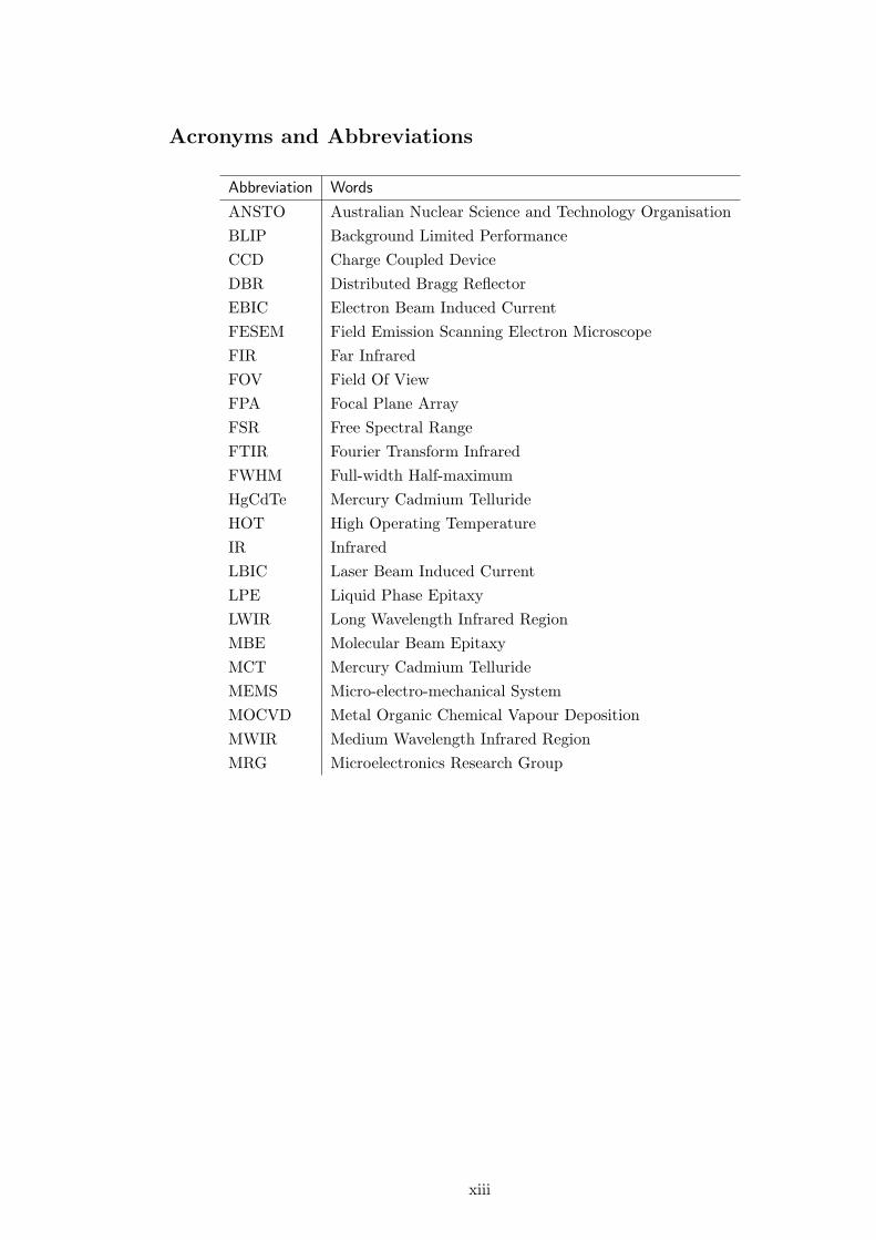
Acronyms and Abbreviations
Abbreviation Words
ANSTO Australian Nuclear Science and Technology Organisation
BLIP Background Limited Performance
CCD Charge Coupled Device
DBR Distributed Bragg Reflector
EBIC Electron Beam Induced Current
FESEM Field Emission Scanning Electron Microscope
FIR Far Infrared
FOV Field Of View
FPA Focal Plane Array
FSR Free Spectral Range
FTIR Fourier Transform Infrared
FWHM Full-width Half-maximum
HgCdTe Mercury Cadmium Telluride
HOT High Operating Temperature
IR Infrared
LBIC Laser Beam Induced Current
LPE Liquid Phase Epitaxy
LWIR Long Wavelength Infrared Region
MBE Molecular Beam Epitaxy
MCT Mercury Cadmium Telluride
MEMS Micro-electro-mechanical System
MOCVD Metal Organic Chemical Vapour Deposition
MWIR Medium Wavelength Infrared Region
MRG Microelectronics Research Group
xiii

Abbreviation Words
NEP Noise Equivalent Power
NIR Near Infrared
PCB Printed Circuit Board
QDIP Quantum-dot Infrared Photodetectors
QMSA Quantitative Mobility Spectrum Analysis
QWIP Quantum Well Infrared Photodetectors
QWS Quarter-wave Stack
RCE Resonant-cavity-enhanced
RHEED Reflection High Energy Electron Diffraction
RIE Reactive Ion Etch
RMS Root Mean Square
RF Radio Frequency
SCR Signal-to-clutter Ratio
SEM Scanning Electron Microscope
SIMS Secondary Ion Mass Spectroscopy
SLM Scanning Laser Microscope
SNR Signal-to-noise Ratio
SRH Shockley-Read-Hall
SWIR Short Wavelength Infrared Region
UHV Ultra-high Vacuum
UWA University of Western Australia
VCSEL Vertical Cavity Surface Emitting Laser
VLWIR Very Long Wavelength Infrared Region
xiv
Symbols
Symbol Description Units
A Optical area of detector cm2
AMJ Area of metallurgical junction cm2
A Absorptance (unitless)
Cd Common difference (unitless)
Cn Capture coefficient for electrons cm3s−1
Cp Capture coefficient for holes cm3s−1
Cr Common ratio (unitless)
c Speed of light: 3.00 × 10⁸ ms−1
D∗ Detectivity cmHz1/2/W
De Diffusion coefficient of electrons in p-type material cm2 s−1
Dh Diffusion coefficient of holes in n-type material cm2 s−1
d Detector thickness cm
Eb Electric bias field V cm−1
Eg Band-gap energy eV
Et Trap energy eV
F Finesse (unitless)
G Photoconductor conductance S
GR Generation rate variable s−1
h Planck’s constant: 6.63 × 10⁻³⁴ J s
Je Drift current density of electrons in p-type material A cm−2
JGRCurrent density due to generation and recombination
in the space charge regionA cm−2
Jh Drift current density of holes in n-type material A cm−2
k Boltzmann’s constant: 8.62 × 10⁻⁵ e V K−1
k imaginary part of refractive index (unitless)
Ld Thickness of absorber in RCE structure µm
Le Diffusion length for electrons in p-type material cm
Lh Diffusion length for holes in n-type material cm
l Photoconductor detector length µm
ℓ Cavity Length µm
m Atomic mass kg
m0 Rest mass of electron: 9.11 × 10⁻³¹ kg
m∗e Electron effective mass kg
m∗lh Light hole effective mass kg
m∗hh Heavy hole effective mass kg
xv
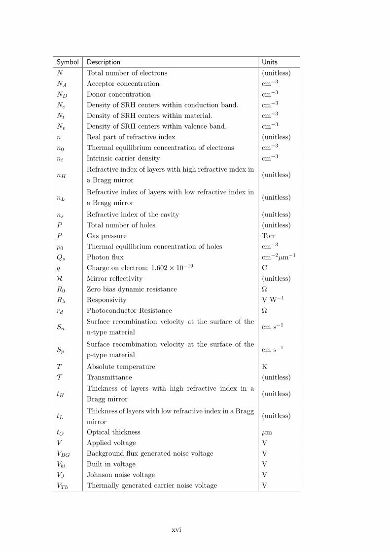
Symbol Description Units
N Total number of electrons (unitless)
NA Acceptor concentration cm−3
ND Donor concentration cm−3
Nc Density of SRH centers within conduction band. cm−3
Nt Density of SRH centers within material. cm−3
Nv Density of SRH centers within valence band. cm−3
n Real part of refractive index (unitless)
n0 Thermal equilibrium concentration of electrons cm−3
ni Intrinsic carrier density cm−3
nHRefractive index of layers with high refractive index in
a Bragg mirror(unitless)
nLRefractive index of layers with low refractive index in
a Bragg mirror(unitless)
ns Refractive index of the cavity (unitless)
P Total number of holes (unitless)
P Gas pressure Torr
p0 Thermal equilibrium concentration of holes cm−3
Qs Photon flux cm−2µm−1
q Charge on electron: 1.602 × 10⁻¹⁹ C
R Mirror reflectivity (unitless)
R0 Zero bias dynamic resistance Ω
Rλ Responsivity V W−1
rd Photoconductor Resistance Ω
SnSurface recombination velocity at the surface of the
n-type materialcm s−1
SpSurface recombination velocity at the surface of the
p-type materialcm s−1
T Absolute temperature K
T Transmittance (unitless)
tHThickness of layers with high refractive index in a
Bragg mirror(unitless)
tLThickness of layers with low refractive index in a Bragg
mirror(unitless)
tO Optical thickness µm
V Applied voltage V
VBG Background flux generated noise voltage V
Vbi Built in voltage V
VJ Johnson noise voltage V
VTh Thermally generated carrier noise voltage V
xvi
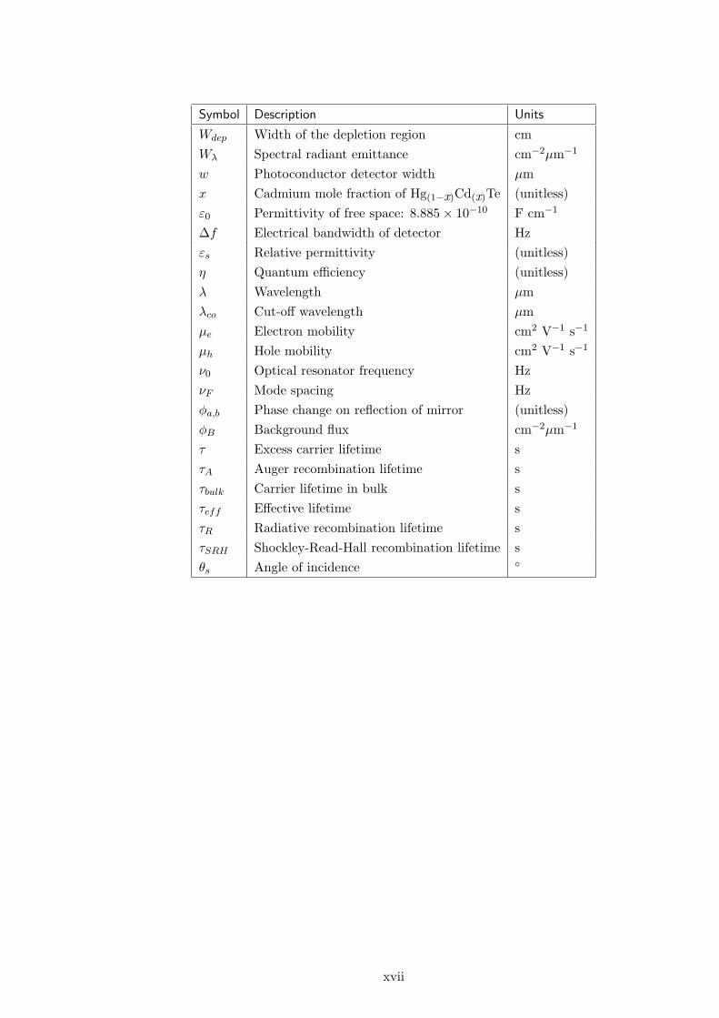
Symbol Description Units
Wdep Width of the depletion region cm
Wλ Spectral radiant emittance cm−2µm−1
w Photoconductor detector width µm
x Cadmium mole fraction of Hg(1−x)Cd(x)Te (unitless)
ε0 Permittivity of free space: 8.885 × 10⁻¹⁰ F cm−1
∆f Electrical bandwidth of detector Hz
εs Relative permittivity (unitless)
η Quantum efficiency (unitless)
λ Wavelength µm
λco Cut-off wavelength µm
µe Electron mobility cm2 V−1 s−1
µh Hole mobility cm2 V−1 s−1
ν0 Optical resonator frequency Hz
νF Mode spacing Hz
φa,b Phase change on reflection of mirror (unitless)
φB Background flux cm−2µm−1
τ Excess carrier lifetime s
τA Auger recombination lifetime s
τbulk Carrier lifetime in bulk s
τeff Effective lifetime s
τR Radiative recombination lifetime s
τSRH Shockley-Read-Hall recombination lifetime s
θs Angle of incidence
xvii

xviii
Chapter 1Introduction
1.1 Infrared Radiation
Infrared (IR) radiation was first discovered by Herschel in 1800 using white light dispersed
by a prism and thermometers located beyond the visible red part of the spectrum [1].
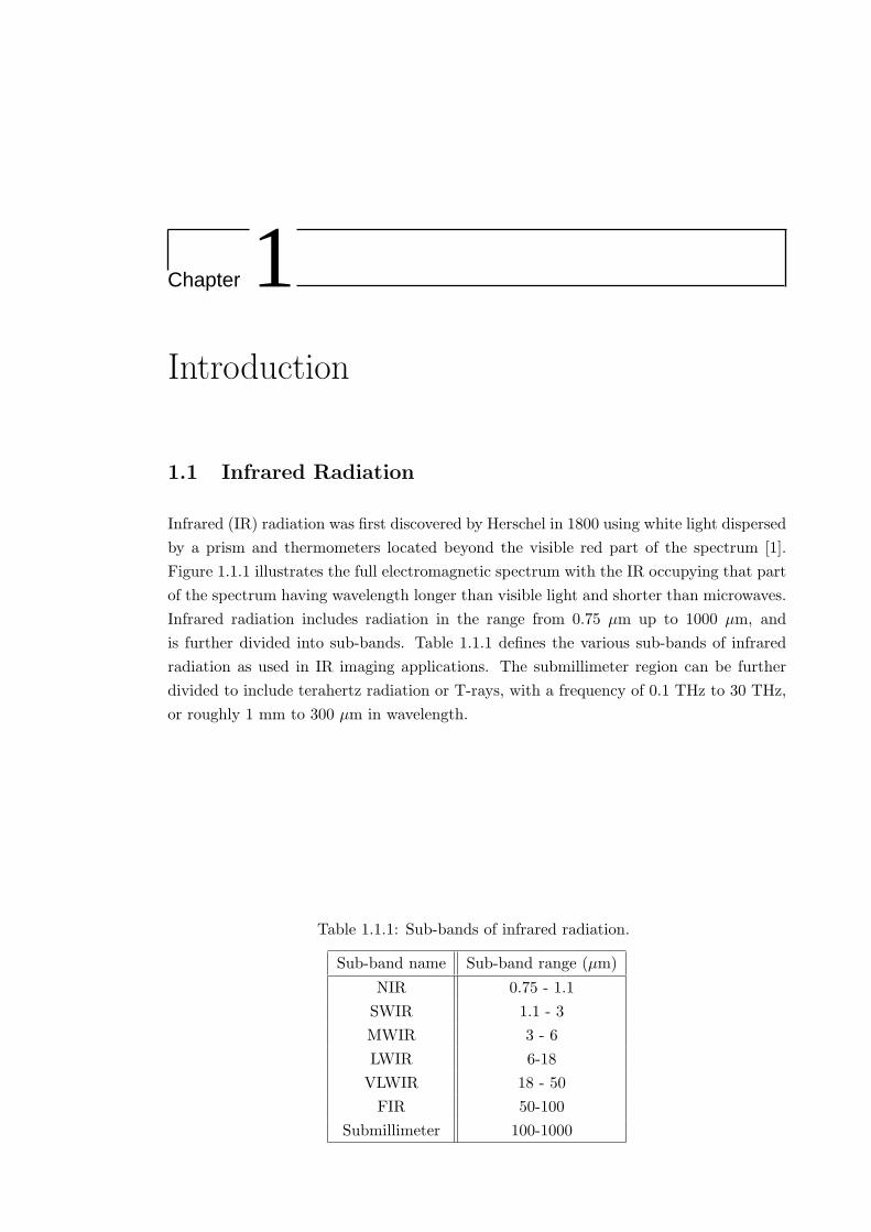
Figure 1.1.1 illustrates the full electromagnetic spectrum with the IR occupying that part
of the spectrum having wavelength longer than visible light and shorter than microwaves.
Infrared radiation includes radiation in the range from 0.75 µm up to 1000 µm, and
is further divided into sub-bands. Table 1.1.1 defines the various sub-bands of infrared
radiation as used in IR imaging applications. The submillimeter region can be further
divided to include terahertz radiation or T-rays, with a frequency of 0.1 THz to 30 THz,
or roughly 1 mm to 300 µm in wavelength.
Table 1.1.1: Sub-bands of infrared radiation.
Sub-band name Sub-band range (µm)
NIR 0.75 - 1.1
SWIR 1.1 - 3
MWIR 3 - 6
LWIR 6-18
VLWIR 18 - 50
FIR 50-100
Submillimeter 100-1000
20 1.1. Infrared Radiation
10 nm-6
10 nm-5
10 nm-4
10 nm-3
10 nm-2
10 nm-1
1 nm
10 nm
100 nm
1 mm
1 m
100 m
10 m
1 km10 km
1 mm
10 mm
100 mm
1 cm
10 cm
700nm
300nmVioletBlueGreenYellowOrangeRed
Gamma Rays
X Rays
Infrared
Microwaves
Radiowaves
UV
Wa
vele
ng
th
Figure 1.1.1: The electromagnetic spectrum.
1.1.1 Blackbody Radiation
All bodies emit electromagnetic radiation that is dependent on their temperature. A
body with an emissivity of unity is said to be a blackbody, or a perfect radiator, and has
a radiated spectrum given by Planck’s law for spectral radiant emittance in Watts cm−2
µm−1 expressed by [2, 3]:
Wλ =2πhc2
λ5
1
exp(
hcλkT
)
− 1
(1.1.1)
where h is Planck’s constant, c is the speed of light, λ is the wavelength, k is Boltz-
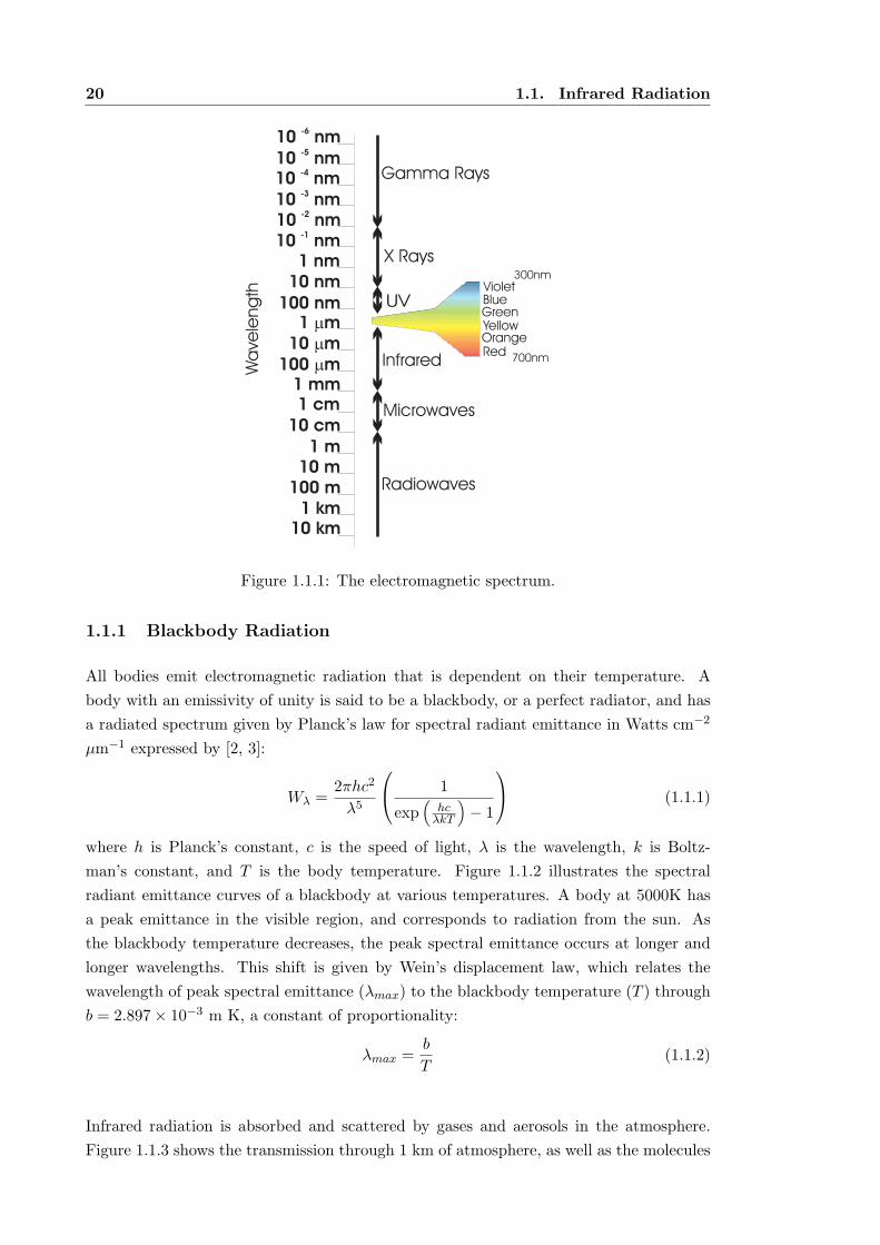
man’s constant, and T is the body temperature. Figure 1.1.2 illustrates the spectral
radiant emittance curves of a blackbody at various temperatures. A body at 5000K has
a peak emittance in the visible region, and corresponds to radiation from the sun. As
the blackbody temperature decreases, the peak spectral emittance occurs at longer and
longer wavelengths. This shift is given by Wein’s displacement law, which relates the
wavelength of peak spectral emittance (λmax) to the blackbody temperature (T ) through
b = 2.897 × 10⁻³ m K, a constant of proportionality:
λmax =b
T(1.1.2)
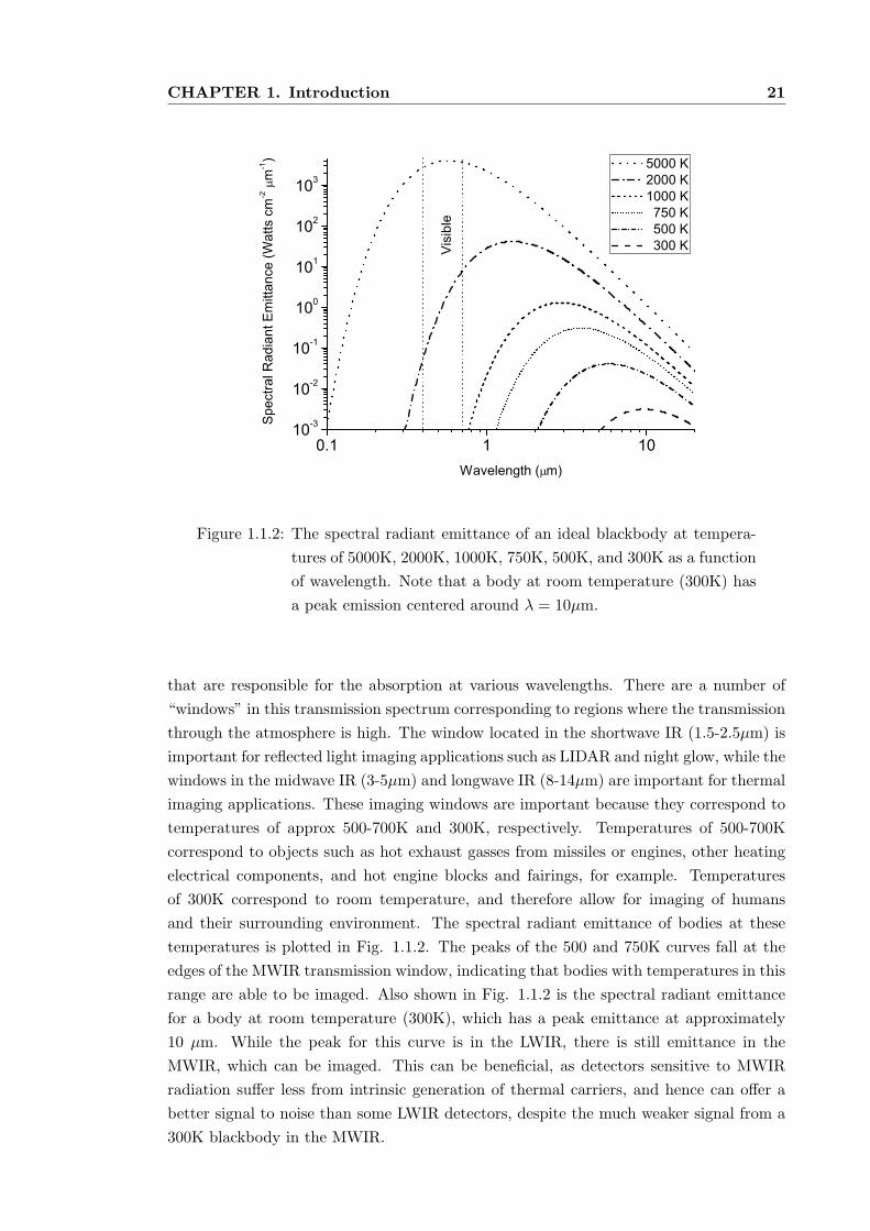
Infrared radiation is absorbed and scattered by gases and aerosols in the atmosphere.
Figure 1.1.3 shows the transmission through 1 km of atmosphere, as well as the molecules
CHAPTER 1. Introduction 21
0.1 1 1010-3
10-2
10-1
100
101
102
103
Spe
ctra
l Rad
iant
Em
ittan
ce (W
atts
cm
-2
m-1)
Wavelength ( m)
5000 K 2000 K 1000 K 750 K 500 K 300 KV
isib
le
Figure 1.1.2: The spectral radiant emittance of an ideal blackbody at tempera-
tures of 5000K, 2000K, 1000K, 750K, 500K, and 300K as a function
of wavelength. Note that a body at room temperature (300K) has
a peak emission centered around λ = 10µm.
that are responsible for the absorption at various wavelengths. There are a number of
“windows” in this transmission spectrum corresponding to regions where the transmission
through the atmosphere is high. The window located in the shortwave IR (1.5-2.5µm) is
important for reflected light imaging applications such as LIDAR and night glow, while the
windows in the midwave IR (3-5µm) and longwave IR (8-14µm) are important for thermal
imaging applications. These imaging windows are important because they correspond to
temperatures of approx 500-700K and 300K, respectively. Temperatures of 500-700K
correspond to objects such as hot exhaust gasses from missiles or engines, other heating
electrical components, and hot engine blocks and fairings, for example. Temperatures
of 300K correspond to room temperature, and therefore allow for imaging of humans
and their surrounding environment. The spectral radiant emittance of bodies at these
temperatures is plotted in Fig. 1.1.2. The peaks of the 500 and 750K curves fall at the
edges of the MWIR transmission window, indicating that bodies with temperatures in this
range are able to be imaged. Also shown in Fig. 1.1.2 is the spectral radiant emittance
for a body at room temperature (300K), which has a peak emittance at approximately
10 µm. While the peak for this curve is in the LWIR, there is still emittance in the
MWIR, which can be imaged. This can be beneficial, as detectors sensitive to MWIR
radiation suffer less from intrinsic generation of thermal carriers, and hence can offer a
better signal to noise than some LWIR detectors, despite the much weaker signal from a
300K blackbody in the MWIR.
22 1.2. Applications of Infrared Sensing
Figure 1.1.3: Transmission through 1km of atmosphere at sea level [3].
1.2 Applications of Infrared Sensing
Infrared sensing has found application in very diverse fields. Present applications can
broadly be split into imaging and spectral sensing. Imaging applications generally em-
ploy focal plane array (FPA) technology to view a scene in various IR spectral windows.
Examples of this include thermal imaging systems that are commonly used by the mil-
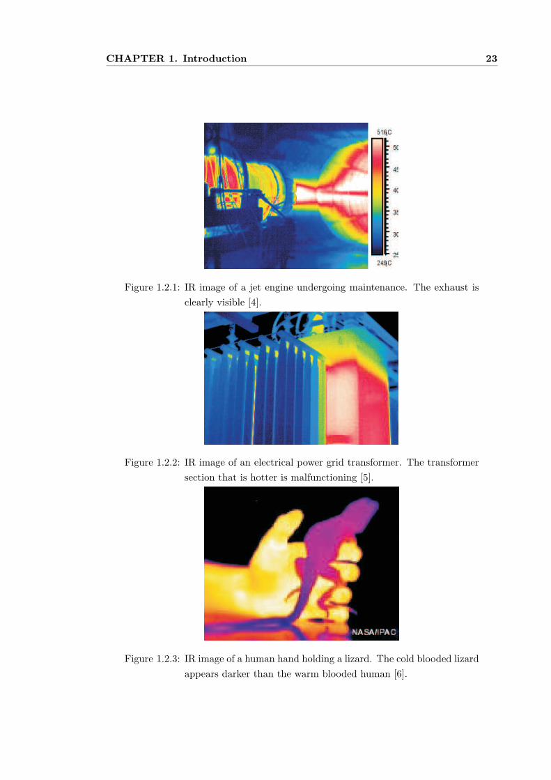
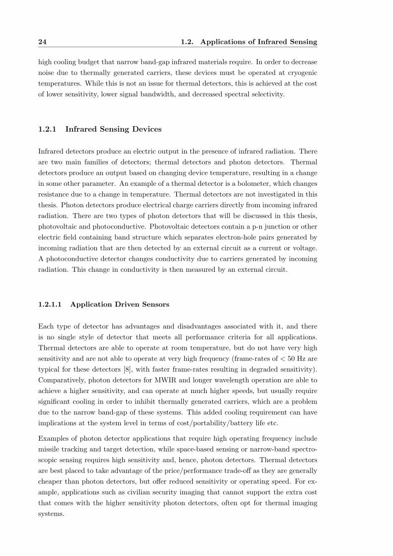
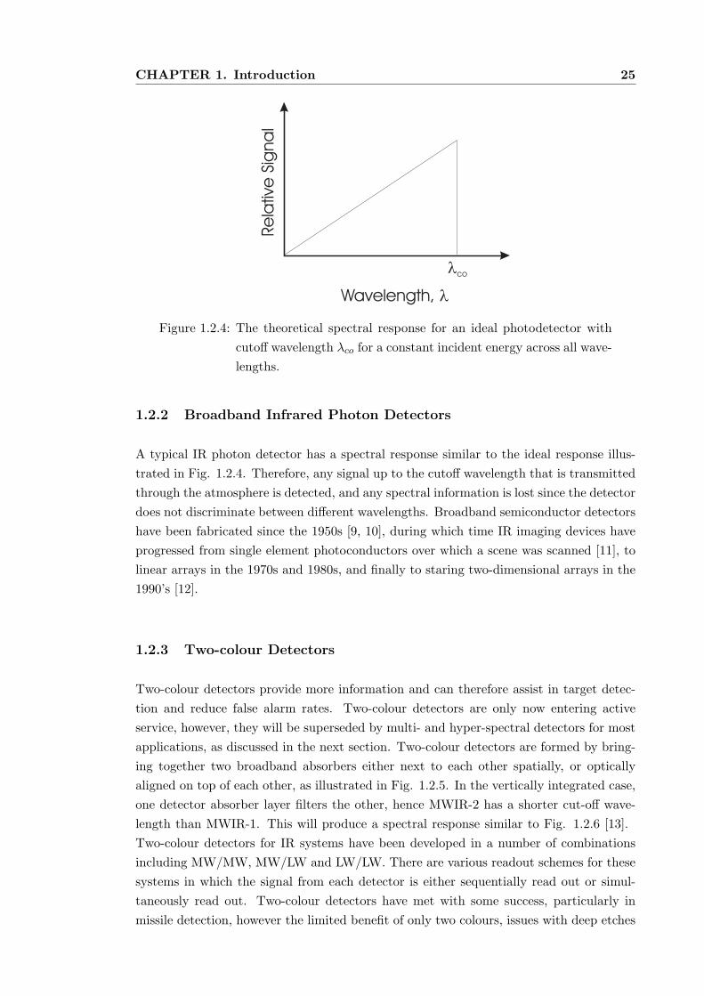
itary, homeland security, maintenance, medical imaging and astronomy. Figures 1.2.1,
1.2.2, and 1.2.3 illustrate some applications of IR imaging. These are typically broad-
band sensors tuned to one IR transmission window, and provide a grey-scale intensity
image based on the number of photons impinging on a given element in the array. The
detecting element provides a signal that represents the integrated photons over the de-
tected wavelength range, which is often displayed as a false-colour image, improving the
human readability of the display. As hot objects emit more photons, the intensity can be
used to give an indication of an objects temperature. A typical use of this is illustrated
by the transformer in Fig. 1.2.2, where the brighter colour of the transformer section
indicates that maintenance is needed on the overheating element, as the oil level is not
sufficient to keep the fins (much colder, and darker) filled and cooling the unit properly.
Spectral sensing provides spectral information about the impinging radiation. This is
achieved by refraction, diffraction or filtering techniques. Spectral information has appli-
cations in a number of fields including process monitoring, pollution monitoring, chemi-
cal/biological sensing, medical imaging and astronomy. Camera systems that discriminate
spectral content are referred to as multi- or hyper-spectral imaging systems. Currently
there is significant research effort in the defence area to fuse imaging with spectral sensing
in order to create imaging systems that provide better target detection [7].
The main impediment to large-scale commercialisation of high sensitivity IR sensing sys-
tems based on photon detectors is the high cost of these systems, which includes the very
CHAPTER 1. Introduction 23
Figure 1.2.1: IR image of a jet engine undergoing maintenance. The exhaust is
clearly visible [4].
Figure 1.2.2: IR image of an electrical power grid transformer. The transformer
section that is hotter is malfunctioning [5].
Figure 1.2.3: IR image of a human hand holding a lizard. The cold blooded lizard
appears darker than the warm blooded human [6].
24 1.2. Applications of Infrared Sensing
high cooling budget that narrow band-gap infrared materials require. In order to decrease
noise due to thermally generated carriers, these devices must be operated at cryogenic
temperatures. While this is not an issue for thermal detectors, this is achieved at the cost
of lower sensitivity, lower signal bandwidth, and decreased spectral selectivity.
1.2.1 Infrared Sensing Devices
Infrared detectors produce an electric output in the presence of infrared radiation. There
are two main families of detectors; thermal detectors and photon detectors. Thermal
detectors produce an output based on changing device temperature, resulting in a change
in some other parameter. An example of a thermal detector is a bolometer, which changes
resistance due to a change in temperature. Thermal detectors are not investigated in this
thesis. Photon detectors produce electrical charge carriers directly from incoming infrared
radiation. There are two types of photon detectors that will be discussed in this thesis,
photovoltaic and photoconductive. Photovoltaic detectors contain a p-n junction or other
electric field containing band structure which separates electron-hole pairs generated by
incoming radiation that are then detected by an external circuit as a current or voltage.
A photoconductive detector changes conductivity due to carriers generated by incoming
radiation. This change in conductivity is then measured by an external circuit.
1.2.1.1 Application Driven Sensors
Each type of detector has advantages and disadvantages associated with it, and there
is no single style of detector that meets all performance criteria for all applications.
Thermal detectors are able to operate at room temperature, but do not have very high
sensitivity and are not able to operate at very high frequency (frame-rates of < 50 Hz are
typical for these detectors [8], with faster frame-rates resulting in degraded sensitivity).
Comparatively, photon detectors for MWIR and longer wavelength operation are able to
achieve a higher sensitivity, and can operate at much higher speeds, but usually require
significant cooling in order to inhibit thermally generated carriers, which are a problem
due to the narrow band-gap of these systems. This added cooling requirement can have
implications at the system level in terms of cost/portability/battery life etc.
Examples of photon detector applications that require high operating frequency include
missile tracking and target detection, while space-based sensing or narrow-band spectro-
scopic sensing requires high sensitivity and, hence, photon detectors. Thermal detectors
are best placed to take advantage of the price/performance trade-off as they are generally
cheaper than photon detectors, but offer reduced sensitivity or operating speed. For ex-
ample, applications such as civilian security imaging that cannot support the extra cost
that comes with the higher sensitivity photon detectors, often opt for thermal imaging
systems.
CHAPTER 1. Introduction 25
Re
lativ
e S
igna
l
Wavelength, l
lco
Figure 1.2.4: The theoretical spectral response for an ideal photodetector with
cutoff wavelength λco for a constant incident energy across all wave-
lengths.
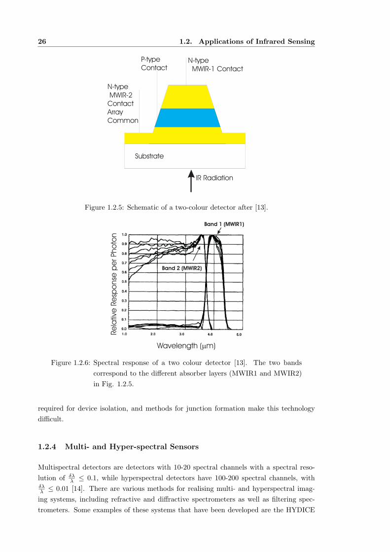
1.2.2 Broadband Infrared Photon Detectors
A typical IR photon detector has a spectral response similar to the ideal response illus-
trated in Fig. 1.2.4. Therefore, any signal up to the cutoff wavelength that is transmitted
through the atmosphere is detected, and any spectral information is lost since the detector
does not discriminate between different wavelengths. Broadband semiconductor detectors
have been fabricated since the 1950s [9, 10], during which time IR imaging devices have
progressed from single element photoconductors over which a scene was scanned [11], to
linear arrays in the 1970s and 1980s, and finally to staring two-dimensional arrays in the
1990’s [12].
1.2.3 Two-colour Detectors
Two-colour detectors provide more information and can therefore assist in target detec-
tion and reduce false alarm rates. Two-colour detectors are only now entering active
service, however, they will be superseded by multi- and hyper-spectral detectors for most
applications, as discussed in the next section. Two-colour detectors are formed by bring-
ing together two broadband absorbers either next to each other spatially, or optically
aligned on top of each other, as illustrated in Fig. 1.2.5. In the vertically integrated case,
one detector absorber layer filters the other, hence MWIR-2 has a shorter cut-off wave-
length than MWIR-1. This will produce a spectral response similar to Fig. 1.2.6 [13].
Two-colour detectors for IR systems have been developed in a number of combinations
including MW/MW, MW/LW and LW/LW. There are various readout schemes for these
systems in which the signal from each detector is either sequentially read out or simul-
taneously read out. Two-colour detectors have met with some success, particularly in
missile detection, however the limited benefit of only two colours, issues with deep etches
26 1.2. Applications of Infrared Sensing
Substrate
N-typeMWIR-2
ContactArrayCommon
P-typeContact
N-typeMWIR-1 Contact
IR Radiation
Figure 1.2.5: Schematic of a two-colour detector after [13].
Re
lativ
e R
esp
onse
pe
r Pho
ton
Wavelength ( m)m
Band 1 (MWIR1)
Band 2 (MWIR2)
Figure 1.2.6: Spectral response of a two colour detector [13]. The two bands
correspond to the different absorber layers (MWIR1 and MWIR2)
in Fig. 1.2.5.
required for device isolation, and methods for junction formation make this technology
difficult.
1.2.4 Multi- and Hyper-spectral Sensors
Multispectral detectors are detectors with 10-20 spectral channels with a spectral reso-
lution of δλλ ≤ 0.1, while hyperspectral detectors have 100-200 spectral channels, with
δλλ ≤ 0.01 [14]. There are various methods for realising multi- and hyperspectral imag-
ing systems, including refractive and diffractive spectrometers as well as filtering spec-
trometers. Some examples of these systems that have been developed are the HYDICE
CHAPTER 1. Introduction 27
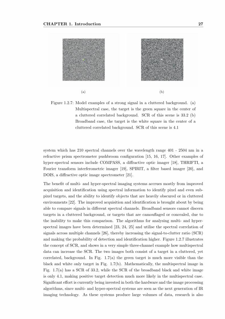
(a) (b)
Figure 1.2.7: Model examples of a strong signal in a cluttered background. (a)
Multispectral case, the target is the green square in the center of
a cluttered correlated background. SCR of this scene is 33.2 (b)
Broadband case, the target is the white square in the center of a
cluttered correlated background. SCR of this scene is 4.1
system which has 210 spectral channels over the wavelength range 401 - 2504 nm in a
refractive prism spectrometer pushbroom configuration [15, 16, 17]. Other examples of
hyper-spectral sensors include COMPASS, a diffractive optic imager [18], THRIFTI, a
Fourier transform interferometric imager [19], SPIRIT, a filter based imager [20], and
DOIS, a diffractive optic image spectrometer [21].
The benefit of multi- and hyper-spectral imaging systems accrues mostly from improved
acquisition and identification using spectral information to identify pixel and even sub-
pixel targets, and the ability to identify objects that are heavily obscured or in cluttered
environments [22]. The improved acquisition and identification is brought about by being
able to compare signals in different spectral channels. Broadband sensors cannot discern
targets in a cluttered background, or targets that are camouflaged or concealed, due to
the inability to make this comparison. The algorithms for analysing multi- and hyper-
spectral images have been determined [23, 24, 25] and utilise the spectral correlation of
signals across multiple channels [26], thereby increasing the signal-to-clutter ratio (SCR)
and making the probability of detection and identification higher. Figure 1.2.7 illustrates
the concept of SCR, and shows in a very simple three-channel example how multispectral
data can increase the SCR. The two images both consist of a target in a cluttered, yet
correlated, background. In Fig. 1.7(a) the green target is much more visible than the
black and white only target in Fig. 1.7(b). Mathematically, the multispectral image in
Fig. 1.7(a) has a SCR of 33.2, while the SCR of the broadband black and white image
is only 4.1, making positive target detection much more likely in the multispectral case.
Significant effort is currently being invested in both the hardware and the image processing
algorithms, since multi- and hyper-spectral systems are seen as the next generation of IR
imaging technology. As these systems produce large volumes of data, research is also
28 1.2. Applications of Infrared Sensing
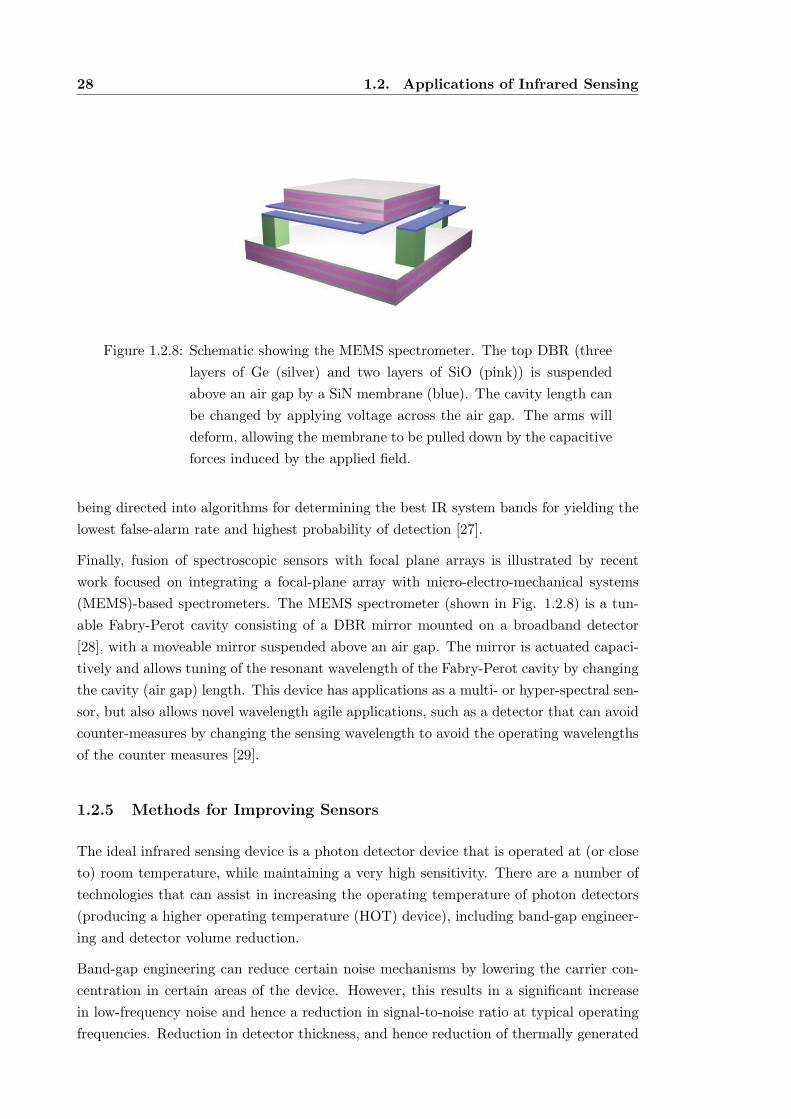
Figure 1.2.8: Schematic showing the MEMS spectrometer. The top DBR (three
layers of Ge (silver) and two layers of SiO (pink)) is suspended
above an air gap by a SiN membrane (blue). The cavity length can
be changed by applying voltage across the air gap. The arms will
deform, allowing the membrane to be pulled down by the capacitive
forces induced by the applied field.
being directed into algorithms for determining the best IR system bands for yielding the
lowest false-alarm rate and highest probability of detection [27].
Finally, fusion of spectroscopic sensors with focal plane arrays is illustrated by recent
work focused on integrating a focal-plane array with micro-electro-mechanical systems
(MEMS)-based spectrometers. The MEMS spectrometer (shown in Fig. 1.2.8) is a tun-
able Fabry-Perot cavity consisting of a DBR mirror mounted on a broadband detector
[28], with a moveable mirror suspended above an air gap. The mirror is actuated capaci-
tively and allows tuning of the resonant wavelength of the Fabry-Perot cavity by changing
the cavity (air gap) length. This device has applications as a multi- or hyper-spectral sen-
sor, but also allows novel wavelength agile applications, such as a detector that can avoid
counter-measures by changing the sensing wavelength to avoid the operating wavelengths
of the counter measures [29].
1.2.5 Methods for Improving Sensors
The ideal infrared sensing device is a photon detector device that is operated at (or close
to) room temperature, while maintaining a very high sensitivity. There are a number of
technologies that can assist in increasing the operating temperature of photon detectors
(producing a higher operating temperature (HOT) device), including band-gap engineer-
ing and detector volume reduction.
Band-gap engineering can reduce certain noise mechanisms by lowering the carrier con-
centration in certain areas of the device. However, this results in a significant increase
in low-frequency noise and hence a reduction in signal-to-noise ratio at typical operating
frequencies. Reduction in detector thickness, and hence reduction of thermally generated
CHAPTER 1. Introduction 29
noise, can also be used to increase operating temperature. However, these devices suf-
fer from reduced absorption of photons and hence suffer from poor quantum efficiency,
making them less attractive. Resonant-cavity-enhanced (RCE) detectors reduce volume
while maintaining high quantum efficiency. This is achieved by placing the absorber
layer within an optical resonant cavity, which in effect allows multiple passes of radiation
through the absorbing layer. Hence, RCE detectors have improved signal-to-noise ratio
at a given operating temperature, possibly a faster operating frequency, and a narrower
optical bandwidth, only showing high quantum efficiency at wavelengths close to the cav-
ity resonance. This may be a hinderance for broad-band imaging, but is acceptable for
multi- and hyper-spectral imaging or spectral sensing. The fact that not only high op-
erating temperature can be achieved, but that higher signal-to-noise ratio and operating
frequency are also achievable, makes RCE detectors an interesting area of research.
1.3 Thesis Objectives
Improving the present generation of infrared imaging systems requires increasing the
operating temperature of photon detectors, while maintaining noise performance, and also
increasing device functionality by introducing features such as multi- and hyper-spectral
imaging. Resonant-cavity-enhanced (RCE) detectors are devices that can achieve all of
these outcomes. Therefore, this thesis will:
• Investigate resonant-cavity-enhancement and the benefits of RCE photon detectors.
• Model RCE devices and design a structure to prove the concept of resonant cavity
enhancement using the Hg(1−x)Cd(x)Te material system.
• Fabricate mirror structures and RCE detector material structures, and separately
characterise their optical performance.
• Fabricate devices from the RCE detector material structures and characterise device
performance, showing that resonant-cavity-enhanced performance is possible for
HgCdTe-based IR detectors.
1.3.1 Thesis Structure
The six chapters of this thesis begin with this introductory chapter. Chapter 2 investi-
gates the materials used for infrared sensing and photon detecting devices that can be
fabricated from these materials. It summarises performance metrics and figures of merit
for comparing detectors, as well as techniques for measuring these metrics. Chapter 3
introduces the concept of resonant-cavity-enhanced detectors, provides modelling results,
and discusses the advantages and disadvantages of this technique for improving device
performance. Also presented in chapter 3 is a discussion on the techniques used to grow
RCE structures, in particular molecular beam epitaxy (MBE), which is used to grow the

30 1.3. Thesis Objectives
mirrors and absorbing layers discussed in chapter 4 and chapter 5. Mirror design, fabri-
cation, and characterisation are discussed in chapter 4, including characterisation before
and after annealing, and characterisation of the refractive index of the CdTe material
used in the mirror structure. Design of resonant-cavity-enhanced detectors is discussed
in chapter 5, as well as results of fabrication and characterisation of RCE detectors, in-
cluding optical cut-off measurements, responsivity measurements, lifetime extraction, and
spatial photoresponse. The outcomes of this thesis are summarised in chapter 6. Mod-
eling details are given in the appendices, along with processing techniques, and a list of
the authors publications that have resulted from this work.
Chapter 2Infrared Detectors
2.1 Introduction
As discussed in section 1.2.1, infrared photon detectors give the highest performance (in
terms of speed, signal, etc.) at the cost of increased system overhead due to the strict
cooling requirements . This chapter investigates different detector types, device structures
for photon detectors and material systems used to create infrared detectors. It introduces
important material properties such as absorption co-efficient and lifetime, device perfor-
mance metrics including quantum efficiency, cut-off wavelength, dark current and noise,
and a variety of figures of merit used to evaluate and compare device performance.
2.2 Detector Types
2.2.1 Thermal Detectors
Thermal detectors operate by absorbing thermal radiation, causing a change in the tem-
perature of the device, which can then be sensed. There are a number of different types
of thermal detectors, including bolometers, thermocouples, and pyroelectric detectors.
Bolometers are the general name given to a large range of thermal detectors where in-
cident radiation is used to heat an absorbing material connected to a heat sink. This
temperature is then measured [30]. There are various ways of achieving this, frequently
with temperature dependent resistors (TDRs), a material which changes resistance with
temperature. The earliest bolometers had a simple design with two strips of platinum
covered with lampblack and arranged in a wheatstone bridge configuration [30]. State of
the art micro-bolometers use vanadium oxide as the TDR material, suspended above a
low-Q micro-machined optically resonant cavity to increase sensitivity [31].
Thermocouples and thermopiles rely on the thermoelectric effect, which occurs when
two different metals or semiconductors experience a temperature gradient, generating a
32 2.2. Detector Types
substrate
Contactpads
d
wl
mesaisolation
Figure 2.2.1: Isometric schematic of a typical photoconductor.
voltage [32]. Pyroelectric detectors rely on materials that develop a charge in the presence
of a temperature gradient: as the material heats, charges move towards opposite surfaces
generating an electric potential. Thermal detectors have a severe trade-off between speed
and sensitivity; with highly sensitive devices requiring significant thermal isolation which,
in turn, results in slow response.
2.2.2 Photon Detectors
Photon detectors work by absorbing incoming photons of infrared wavelength light, con-
verting these photons to free carriers (electrons, holes, or both electrons and holes), and
then sensing the resulting electrical signal. There are two types of photon detectors, pho-
tovoltaic and photoconductive. Photovoltaic detectors contain a p-n junction (or other
field-generating band structure), and carriers generated by incoming radiation are sepa-
rated by the built-in electric field of the junction and detected by an external circuit as
a current or voltage. A photoconductive detector relies on changes in the conductivity
of an absorbing material due to carriers generated by incoming radiation, which is then
measured by an external circuit.
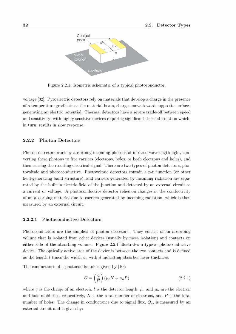
2.2.2.1 Photoconductive Detectors
Photoconductors are the simplest of photon detectors. They consist of an absorbing
volume that is isolated from other devices (usually by mesa isolation) and contacts on
either side of the absorbing volume. Figure 2.2.1 illustrates a typical photoconductive
device. The optically active area of the device is between the two contacts and is defined
as the length l times the width w, with d indicating absorber layer thickness.
The conductance of a photoconductor is given by [10]:
G =
(
q
l2
)
(µeN + µhP ) (2.2.1)
where q is the charge of an electron, l is the detector length, µe and µh are the electron
and hole mobilities, respectively, N is the total number of electrons, and P is the total
number of holes. The change in conductance due to signal flux, Qs, is measured by an
external circuit and is given by:
CHAPTER 2. Infrared Detectors 33
∆G =
(
q
l2
)
(µe∆N + µh∆P ) (2.2.2)
=
(
q
l2
)
µhτ
[∫ ∞
0Qs (λ) η (λ)A
]
[1 + b] (2.2.3)
where:
b =µe
µh(2.2.4)
The number of excess carriers under steady state illumination are denoted by ∆N and
∆P , Qs is the signal photon flux, η is the quantum efficiency, and τ is the effective excess
carrier lifetime. The expression for b is only valid if ∆N = ∆P , which holds in the absence
of significant trap mediated recombination [10].
As photoconductors have such a simple internal band structure, there are few avenues
to improve device performance by band-structure engineering. Most focus has been on
improving performance by adjusting the band structure at the contacts. Blocking contacts
engineer the band structure in order to prevent minority carriers from easily reaching the
contacts, thereby increasing the effective lifetime. Another method of improving device
performance is by grading the composition of the structure through the thickness. This
can keep carriers away from imperfect surface layers which reduce lifetime [33], and is
used as an adjunct to surface passivation. Materials such as CdTe, ZnS and anodic oxide
[34] are used as surface passivants.
Photoconductive devices are used in this work because the fabrication processes and
electrical behaviour are simpler, and are therefore more easily controlled and modelled.
However, photoconductive devices are not practical for use in focal plane array type
applications, as the bias voltage needed for device operation leads to a large static power
dissipation. Furthermore, photoconductors cannot physically realise the high fill factors
that are required for focal plane arrays. Finally, as will be shown later in this thesis,
photoconductors are not ideal devices for resonant-cavity-enhanced detectors due to the
increased impact of surface recombination on thin photoconductor structures.
2.2.2.2 Photovoltaic Detectors
Photovoltaic devices incorporate a built-in field to separate carriers, which can be created
at some form of metallurgical junction, such as when a p-type semiconductor is brought
into intimate contact with an n-type semiconductor, making a p-n junction, or metal and
semiconductor with different work functions are brought together, creating a Schottky
barrier. In terms of a p-n junction, if the material for both the p-type material and the
n-type material is the same (i.e. has the same band-gap, electron affinity, etc.), then
the junction is said to be a homojunction. If the two materials have different band-gaps
and/or work functions, then the junction is a heterojunction.
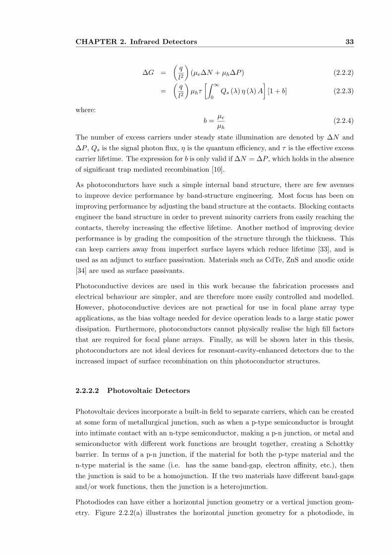
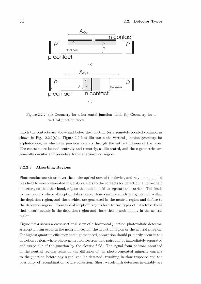
Photodiodes can have either a horizontal junction geometry or a vertical junction geom-
etry. Figure 2.2.2(a) illustrates the horizontal junction geometry for a photodiode, in
34 2.2. Detector Types
AOpt
p pnn contact
p contact
a
dthickness
(a)
AOpt
p pn
n contactp contact
ad thickness
(b)
Figure 2.2.2: (a) Geometry for a horizontal junction diode (b) Geometry for a
vertical junction diode.
which the contacts are above and below the junction (or a remotely located common as
shown in Fig. 2.2.2(a)). Figure 2.2.2(b) illustrates the vertical junction geometry for
a photodiode, in which the junction extends through the entire thickness of the layer.
The contacts are located centrally and remotely, as illustrated, and these geometries are
generally circular and provide a toroidal absorption region.
2.2.2.3 Absorbing Regions
Photoconductors absorb over the entire optical area of the device, and rely on an applied
bias field to sweep generated majority carriers to the contacts for detection. Photovoltaic
detectors, on the other hand, rely on the built-in field to separate the carriers. This leads
to two regions where absorption takes place, those carriers which are generated within
the depletion region, and those which are generated in the neutral region and diffuse to
the depletion region. These two absorption regions lead to two types of detectors: those
that absorb mainly in the depletion region and those that absorb mainly in the neutral
region.
Figure 2.2.3 shows a cross-sectional view of a horizontal junction photovoltaic detector.
Absorption can occur in the neutral n-region, the depletion region or the neutral p-region.
For highest quantum efficiency and highest speed, absorption should primarily occur in the
depletion region, where photo-generated electron-hole pairs can be immediately separated
and swept out of the junction by the electric field. The signal from photons absorbed
in the neutral regions relies on the diffusion of the photo-generated minority carriers
to the junction before any signal can be detected, resulting in slow response and the
possibility of recombination before collection. Short wavelength detectors invariably are
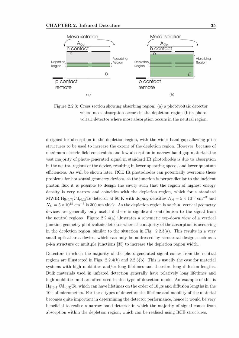
CHAPTER 2. Infrared Detectors 35
AOpt
p
nn contact
p contactremote
Mesa isolation
DepletionRegion
AbsorbingRegion
(a)
AOpt
p
nn contact
p contactremote
Mesa isolation
DepletionRegion
AbsorbingRegion
(b)
Figure 2.2.3: Cross section showing absorbing region: (a) a photovoltaic detector
where most absorption occurs in the depletion region (b) a photo-
voltaic detector where most absorption occurs in the neutral region.
designed for absorption in the depletion region, with the wider band-gap allowing p-i-n
structures to be used to increase the extent of the depletion region. However, because of
maximum electric field constraints and low absorption in narrow band-gap materials,the
vast majority of photo-generated signal in standard IR photodiodes is due to absorption
in the neutral regions of the device, resulting in lower operating speeds and lower quantum
efficiencies. As will be shown later, RCE IR photodiodes can potentially overcome these
problems for horizontal geometry devices, as the junction is perpendicular to the incident
photon flux it is possible to design the cavity such that the region of highest energy
density is very narrow and coincides with the depletion region, which for a standard
MWIR Hg(0.7)Cd(0.3)Te detector at 80 K with doping densities NA = 5 × 1016 cm−3 and
ND = 5×1015 cm−3 is 300 nm thick. As the depletion region is so thin, vertical geometry
devices are generally only useful if there is significant contribution to the signal from
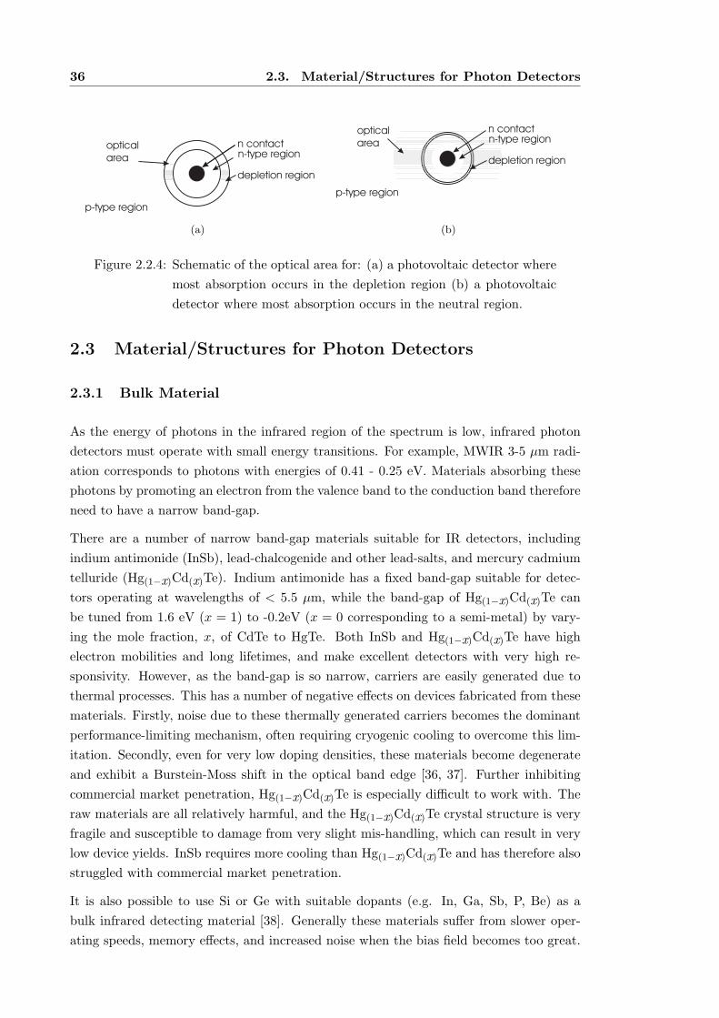
the neutral regions. Figure 2.2.4(a) illustrates a schematic top-down view of a vertical
junction geometry photovoltaic detector where the majority of the absorption is occurring
in the depletion region, similar to the situation in Fig. 2.2.3(a). This results in a very
small optical area device, which can only be addressed by structural design, such as a
p-i-n structure or multiple junctions [35] to increase the depletion region width.
Detectors in which the majority of the photo-generated signal comes from the neutral
regions are illustrated in Figs. 2.2.4(b) and 2.2.3(b). This is usually the case for material
systems with high mobilities and/or long lifetimes and therefore long diffusion lengths.
Bulk materials used in infrared detection generally have relatively long lifetimes and
high mobilities and are often used in this type of detection mode. An example of this is
Hg(0.4)Cd(0.3)Te, which can have lifetimes on the order of 10 µs and diffusion lengths in the
10’s of micrometers. For these types of detectors the lifetime and mobility of the material
becomes quite important in determining the detector performance, hence it would be very
beneficial to realise a narrow-band detector in which the majority of signal comes from
absorption within the depletion region, which can be realised using RCE structures.
36 2.3. Material/Structures for Photon Detectors
n-type regionn contact
depletion region
p-type region
opticalarea
(a)
p-type region
opticalarea n-type region
n contact
depletion region
(b)
Figure 2.2.4: Schematic of the optical area for: (a) a photovoltaic detector where
most absorption occurs in the depletion region (b) a photovoltaic
detector where most absorption occurs in the neutral region.
2.3 Material/Structures for Photon Detectors
2.3.1 Bulk Material
As the energy of photons in the infrared region of the spectrum is low, infrared photon
detectors must operate with small energy transitions. For example, MWIR 3-5 µm radi-
ation corresponds to photons with energies of 0.41 - 0.25 eV. Materials absorbing these
photons by promoting an electron from the valence band to the conduction band therefore
need to have a narrow band-gap.
There are a number of narrow band-gap materials suitable for IR detectors, including
indium antimonide (InSb), lead-chalcogenide and other lead-salts, and mercury cadmium
telluride (Hg(1−x)Cd(x)Te). Indium antimonide has a fixed band-gap suitable for detec-
tors operating at wavelengths of < 5.5 µm, while the band-gap of Hg(1−x)Cd(x)Te can
be tuned from 1.6 eV (x = 1) to -0.2eV (x = 0 corresponding to a semi-metal) by vary-
ing the mole fraction, x, of CdTe to HgTe. Both InSb and Hg(1−x)Cd(x)Te have high
electron mobilities and long lifetimes, and make excellent detectors with very high re-
sponsivity. However, as the band-gap is so narrow, carriers are easily generated due to
thermal processes. This has a number of negative effects on devices fabricated from these
materials. Firstly, noise due to these thermally generated carriers becomes the dominant
performance-limiting mechanism, often requiring cryogenic cooling to overcome this lim-
itation. Secondly, even for very low doping densities, these materials become degenerate
and exhibit a Burstein-Moss shift in the optical band edge [36, 37]. Further inhibiting
commercial market penetration, Hg(1−x)Cd(x)Te is especially difficult to work with. The
raw materials are all relatively harmful, and the Hg(1−x)Cd(x)Te crystal structure is very
fragile and susceptible to damage from very slight mis-handling, which can result in very
low device yields. InSb requires more cooling than Hg(1−x)Cd(x)Te and has therefore also
struggled with commercial market penetration.
It is also possible to use Si or Ge with suitable dopants (e.g. In, Ga, Sb, P, Be) as a
bulk infrared detecting material [38]. Generally these materials suffer from slower oper-
ating speeds, memory effects, and increased noise when the bias field becomes too great.
CHAPTER 2. Infrared Detectors 37
n stacklayers
InAs QD s
GaAsn+
Contact
GaAsBarrier GaAs
n+Contact
Al Ga As
Barrier0.3 0.7
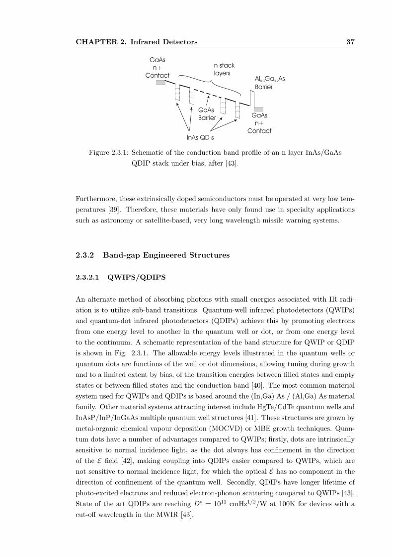
Figure 2.3.1: Schematic of the conduction band profile of an n layer InAs/GaAs
QDIP stack under bias, after [43].
Furthermore, these extrinsically doped semiconductors must be operated at very low tem-
peratures [39]. Therefore, these materials have only found use in specialty applications
such as astronomy or satellite-based, very long wavelength missile warning systems.
2.3.2 Band-gap Engineered Structures
2.3.2.1 QWIPS/QDIPS
An alternate method of absorbing photons with small energies associated with IR radi-
ation is to utilize sub-band transitions. Quantum-well infrared photodetectors (QWIPs)
and quantum-dot infrared photodetectors (QDIPs) achieve this by promoting electrons
from one energy level to another in the quantum well or dot, or from one energy level
to the continuum. A schematic representation of the band structure for QWIP or QDIP
is shown in Fig. 2.3.1. The allowable energy levels illustrated in the quantum wells or
quantum dots are functions of the well or dot dimensions, allowing tuning during growth
and to a limited extent by bias, of the transition energies between filled states and empty
states or between filled states and the conduction band [40]. The most common material
system used for QWIPs and QDIPs is based around the (In,Ga) As / (Al,Ga) As material
family. Other material systems attracting interest include HgTe/CdTe quantum wells and
InAsP/InP/InGaAs multiple quantum well structures [41]. These structures are grown by
metal-organic chemical vapour deposition (MOCVD) or MBE growth techniques. Quan-
tum dots have a number of advantages compared to QWIPs; firstly, dots are intrinsically
sensitive to normal incidence light, as the dot always has confinement in the direction
of the E field [42], making coupling into QDIPs easier compared to QWIPs, which are
not sensitive to normal incidence light, for which the optical E has no component in the
direction of confinement of the quantum well. Secondly, QDIPs have longer lifetime of
photo-excited electrons and reduced electron-phonon scattering compared to QWIPs [43].
State of the art QDIPs are reaching D∗ = 1011 cmHz1/2/W at 100K for devices with a
cut-off wavelength in the MWIR [43].
38 2.4. Material Properties
QWIPs and QDIPs are also affected by thermal generation of carriers and require cryo-
genic cooling. Furthermore, quantum efficiency of detectors made from these materials
is poor due to a low absorption co-efficient. Quantum efficiencies are typically limited to
around 10-20%, which is low compared to the quantum efficiency of detectors fabricated
using direct narrow band-gap materials, which approaches 100%, due to larger absorp-
tion co-efficients and long diffusion lengths. This has restricted QWIPs and QDIPs from
becoming dominant for IR applications.
2.3.2.2 Superlattices
While superlattices are similar in structure to QWIPs, in that they consist of alternating
layers of wide band-gap material and a narrower band-gap material, the principle of op-
eration of these devices is quite different. When the wider band-gap material thickness
is reduced below a critical thickness electrons may tunnel through the barrier so that
electrons may then behave in a fashion similar to electrons in a crystal lattice, effec-
tively creating an engineered bulk material band structure that can be controlled by the
thickness of the layers of the superlattice. Material systems attracting interest include
HgTe/CdTe superlattices [44], and InAs/GaInSb strained layer superlattices [45] to list a
few.
2.4 Material Properties
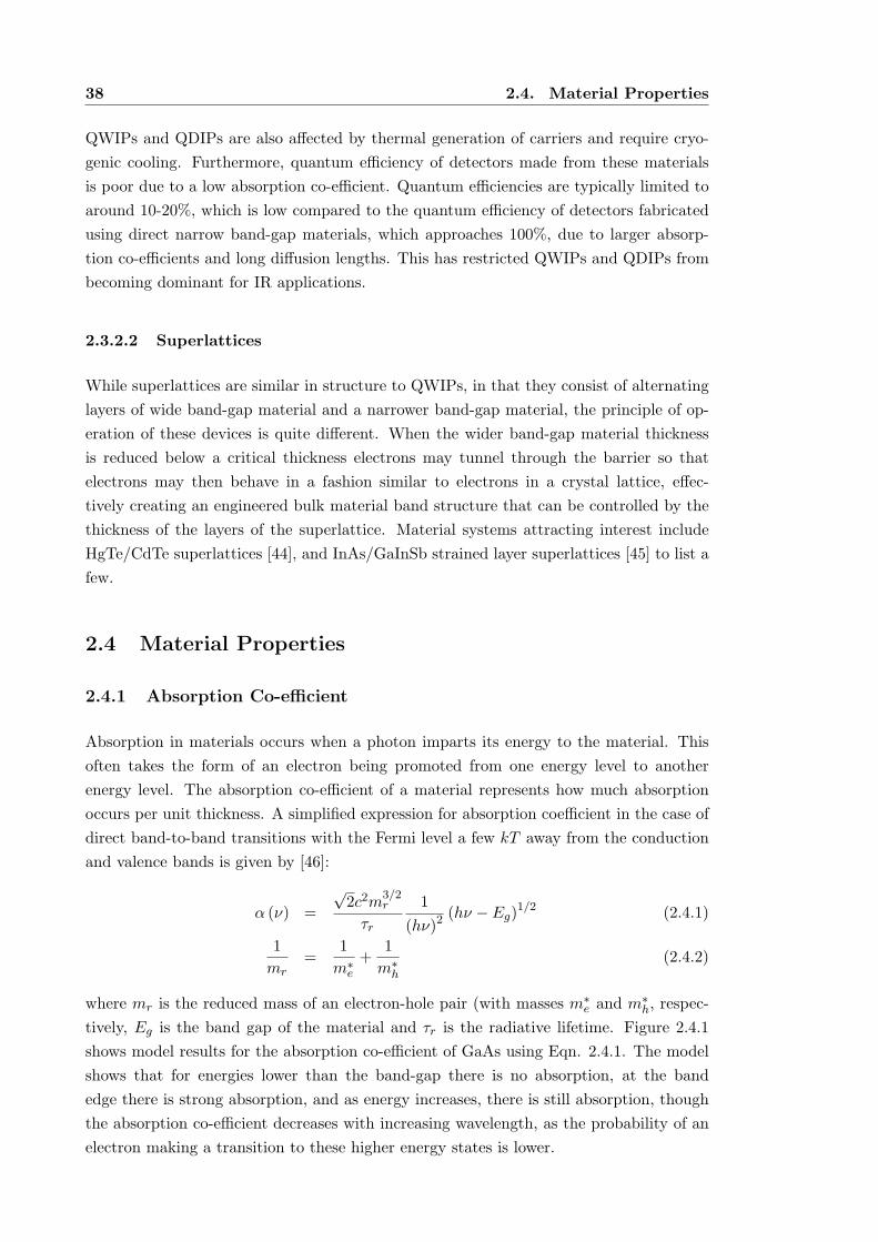
2.4.1 Absorption Co-efficient
Absorption in materials occurs when a photon imparts its energy to the material. This
often takes the form of an electron being promoted from one energy level to another
energy level. The absorption co-efficient of a material represents how much absorption
occurs per unit thickness. A simplified expression for absorption coefficient in the case of
direct band-to-band transitions with the Fermi level a few kT away from the conduction
and valence bands is given by [46]:
α (ν) =
√2c2m
3/2r
τr
1
(hν)2(hν − Eg)
1/2 (2.4.1)
1
mr=
1
m∗e
+1
m∗h
(2.4.2)
where mr is the reduced mass of an electron-hole pair (with masses m∗e and m∗
h, respec-
tively, Eg is the band gap of the material and τr is the radiative lifetime. Figure 2.4.1
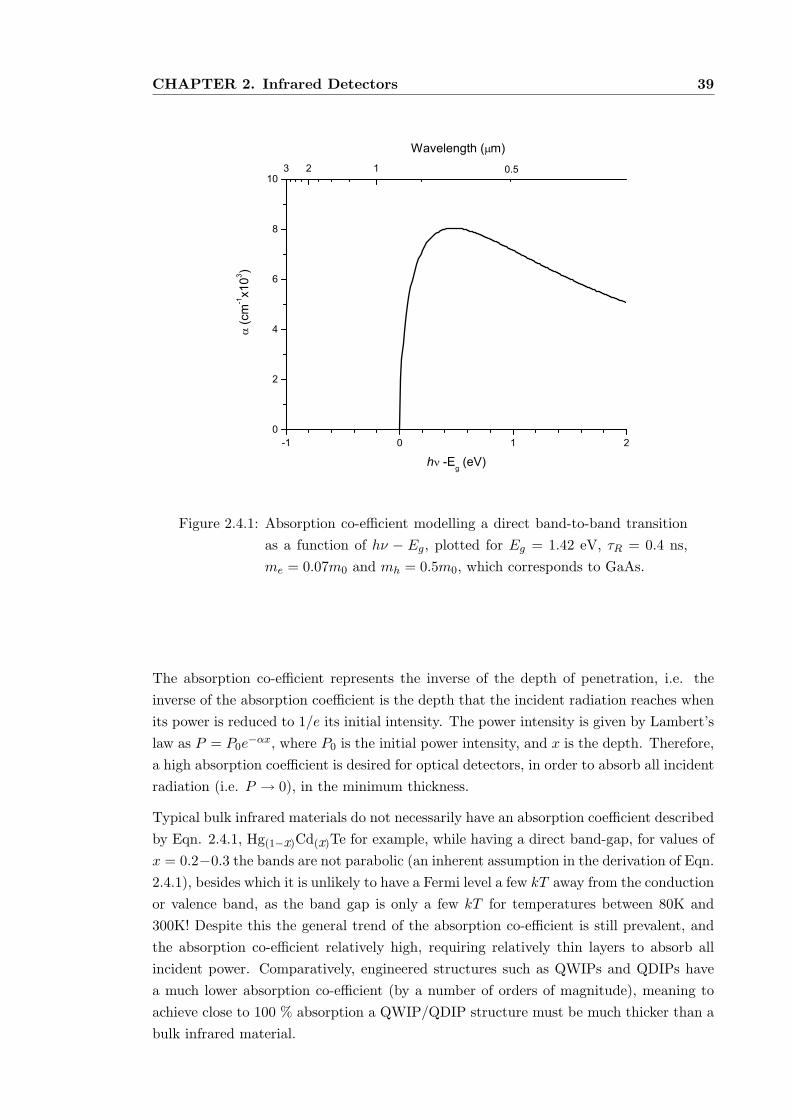
shows model results for the absorption co-efficient of GaAs using Eqn. 2.4.1. The model
shows that for energies lower than the band-gap there is no absorption, at the band
edge there is strong absorption, and as energy increases, there is still absorption, though
the absorption co-efficient decreases with increasing wavelength, as the probability of an
electron making a transition to these higher energy states is lower.
CHAPTER 2. Infrared Detectors 39
-1 0 1 20
2
4
6
8
103 2 1
(cm
-1x1
03 )
h -Eg (eV)
Wavelength ( m)0.5
Figure 2.4.1: Absorption co-efficient modelling a direct band-to-band transition
as a function of hν − Eg, plotted for Eg = 1.42 eV, τR = 0.4 ns,
me = 0.07m0 and mh = 0.5m0, which corresponds to GaAs.
The absorption co-efficient represents the inverse of the depth of penetration, i.e. the
inverse of the absorption coefficient is the depth that the incident radiation reaches when
its power is reduced to 1/e its initial intensity. The power intensity is given by Lambert’s
law as P = P0e−αx, where P0 is the initial power intensity, and x is the depth. Therefore,
a high absorption coefficient is desired for optical detectors, in order to absorb all incident
radiation (i.e. P → 0), in the minimum thickness.
Typical bulk infrared materials do not necessarily have an absorption coefficient described
by Eqn. 2.4.1, Hg(1−x)Cd(x)Te for example, while having a direct band-gap, for values of
x = 0.2−0.3 the bands are not parabolic (an inherent assumption in the derivation of Eqn.
2.4.1), besides which it is unlikely to have a Fermi level a few kT away from the conduction
or valence band, as the band gap is only a few kT for temperatures between 80K and
300K! Despite this the general trend of the absorption co-efficient is still prevalent, and
the absorption co-efficient relatively high, requiring relatively thin layers to absorb all
incident power. Comparatively, engineered structures such as QWIPs and QDIPs have
a much lower absorption co-efficient (by a number of orders of magnitude), meaning to
achieve close to 100 % absorption a QWIP/QDIP structure must be much thicker than a
bulk infrared material.
40 2.4. Material Properties
2.4.2 Lifetime
Carrier lifetime is the average period of time that a carrier exists before recombining
and should be represented by a probability density function. Interest is usually only in
minority carrier lifetimes, because minority carrier density due to injection or optical
generation may be considerably above the thermal equilibrium value. This is compared
with the majority carrier concentration, which is not appreciably changed, compared to
the thermal equilibrium value [47]. Excess minority carrier lifetimes in the bulk of a
semiconductor are affected by three dominant mechanisms, Shockley Read Hall recombi-
nation (SRH), Auger recombination, and radiative recombination, as given in Eqn. 2.4.3.
SRH recombination is material quality dependent, with higher quality material reducing
SRH recombination. Auger recombination and radiative recombination are fundamental
recombination processes where rates are determined by the band structure and doping of
the material.
1
τbulk=
1
τA+
1
τR+
1
τSRH(2.4.3)
where:τbulk is the effective minority carrier lifetime.
τA is the Auger lifetime.
τR is the radiative recombination lifetime.
τSRH is the Shockley Read Hall lifetime.
2.4.2.1 Shockley-Read-Hall Recombination
Shockley-Read-Hall recombination occurs via Shockley-Read-Hall centers. These centers
are defects, which create energy states in the energy band-gap [48]. Figure 2.4.2 shows
recombination via these centers.
The steady-state lifetime of excess holes due to SRH recombination via SRH centers
located at an energy Et below the conduction band is given by [49]:
τp =τp0 (n0 + n1) + τn0 (n0 + n1) τp0Nt
(
1 + n0
n1
)−1
n0 + p0 +Nt
(
1 + n0
n1
)−1 (
1 + n1
n0
)−1 (2.4.4)
The steady-state lifetime of excess electrons is similarly:
τn =τp0 (n0 + n1) + τn0 (n0 + n1) τn0Nt
(
1 + p0
p1
)−1
n0 + p0 +Nt
(
1 + p0
p1
)−1 (
1 + p1
p0
)−1 (2.4.5)
where:
τn0 =1
CnNt
τp0 =1
CpNt
CHAPTER 2. Infrared Detectors 41
n1 = Nc exp
(− (Eg − Et)
kT
)
(2.4.6)
p1 = Nv exp
(− (Et − Ev)
kT
)
(2.4.7)
Nc = 2
(
2πm∗ekT
h2
)1.5
Nv = 2
(
2πm∗hkT
h2
)1.5
p0 =1
2
[
NA +(
N2A + 4n2
i
)0.5]
and
n0 =n2
i
p0
The trap density Nt, and capture coefficients for electrons and holes (Cn, Cp) are all
dependent on the material quality. The effective electron and hole masses (m∗e, m
∗h) are
material dependent. Equations 2.4.6 and 2.4.7 are given by Nemirovsky et al. [50], which
also have approximated the trap energy Et to be
Et =Eg
2+ kT ln
(
m∗h
m∗e
)0.75
− kT ln
(
NA
ni
)
(2.4.8)
2.4.2.2 Auger Recombination
Auger recombination is a direct recombination mechanism, in which the energy of the
recombining carriers is taken by a third carrier, which then usually loses its excess energy
through thermal vibrations. There are a number of different combinations that result
in Auger recombination. For example: Auger1 is direct band-to-band recombination of
an electron with a heavy hole and excitation of another electron in the conduction band
[10, 48], and is shown in Fig. 2.4.3. Auger7 is direct band-to-band recombination leading
to excitation of electron from the light hole to heavy hole band [48]. For narrow band-gap
semiconductors Auger1 and Auger7 are the dominant Auger recombination mechanisms.
The lifetime due to Auger1 recombination is given by:
τA1 =2τA1in
2i
n0 (n0 + p0)(2.4.9)
while for Auger7 recombination the lifetime is given by:
τA7 =2τA7in
2i
p0 (n0 + p0)(2.4.10)
where: τA7i = γτA1i are the intrinsic Auger lifetimes, and are material dependent, and γ
is the ratio between Auger1 and Auger7 intrinsic lifetimes. Combining Auger1 and Auger7
gives the complete Auger lifetime expression as:
1
τA=
1
τA1+
1
τA7(2.4.11)

42 2.4. Material Properties
x x x x
EcEc
Ev
Figure 2.4.2: Shockley-Read-Hall recombination via SRH centers. (a) electron
capture (b) electron emission from center (c) hole capture (d) hole
emission from center.
E
k
E
k
ConductionBand
Heavy HoleBand
Light HoleBand(a) (b)
Figure 2.4.3: Auger Recombination (a)Auger1 (b)Auger7 [10].
EcEc
Ev
Photon
Figure 2.4.4: Radiative Recombination
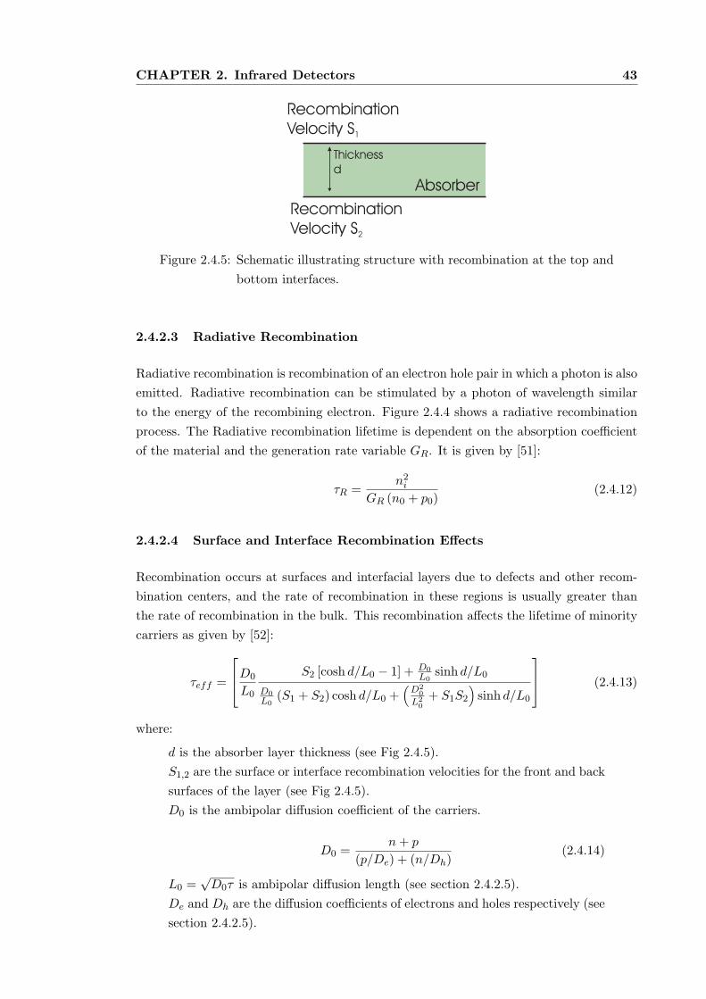
CHAPTER 2. Infrared Detectors 43
Thicknessd
RecombinationVelocity S1
Absorber
RecombinationVelocity S2
Figure 2.4.5: Schematic illustrating structure with recombination at the top and
bottom interfaces.
2.4.2.3 Radiative Recombination
Radiative recombination is recombination of an electron hole pair in which a photon is also
emitted. Radiative recombination can be stimulated by a photon of wavelength similar
to the energy of the recombining electron. Figure 2.4.4 shows a radiative recombination
process. The Radiative recombination lifetime is dependent on the absorption coefficient
of the material and the generation rate variable GR. It is given by [51]:
τR =n2
i
GR (n0 + p0)(2.4.12)
2.4.2.4 Surface and Interface Recombination Effects
Recombination occurs at surfaces and interfacial layers due to defects and other recom-
bination centers, and the rate of recombination in these regions is usually greater than
the rate of recombination in the bulk. This recombination affects the lifetime of minority
carriers as given by [52]:
τeff =
D0
L0
S2 [cosh d/L0 − 1] + D0
L0sinh d/L0
D0
L0(S1 + S2) cosh d/L0 +
(
D20
L20
+ S1S2
)
sinh d/L0
(2.4.13)
where:
d is the absorber layer thickness (see Fig 2.4.5).
S1,2 are the surface or interface recombination velocities for the front and back
surfaces of the layer (see Fig 2.4.5).
D0 is the ambipolar diffusion coefficient of the carriers.
D0 =n+ p
(p/De) + (n/Dh)(2.4.14)
L0 =√D0τ is ambipolar diffusion length (see section 2.4.2.5).
De and Dh are the diffusion coefficients of electrons and holes respectively (see
section 2.4.2.5).
44 2.4. Material Properties
With simplifying assumptions such as device thickness d being much less than the diffusion
length L0, and the recombination velocity being the same at both the front and back
surfaces and equal to S, Eqn. 2.4.13 simplifies to:
1
τeff=
1
τbulk+
2S
d(2.4.15)
The surface recombination velocity is a function of the interface trap density, Dit, and is
given by [53]:
S =kTDit
q
√
CnCp (p0 + n0)
2ni
[
cosh(
(Et−Ei)kT − u0
)
+ cosh
(
(qφs+Ef−Ei)kT − u0
)] (2.4.16)
where Cn, Cp are the electron and hole capture coefficients, respectively, φs is the surface
potential, no and p0 are the equilibrium electron and hole concentrations, respectively,
Ei is the intrinsic energy level, Et is the trap energy level (relative to the intrinsic en-
ergy level), Ef is the fermi energy level, ni is the intrinsic carrier concentration and
u0 = ln (Cn/Cp).
2.4.2.5 Mobility and Diffusion Length
Under the influence of an electric field, the free carriers in a material are accelerated by
the field but also scattered by the lattice. The net result is that for bulk semiconductors of
dimension larger than the mean free path between scattering events, the carriers achieve a
constant average velocity proportional to the electric field. The proportionality constant
is called the mobility and is an important material parameter. In cases where one carrier
is dominant, the conductivity of the material will be directly proportional to the mobility.
Diffusion length is the average distance a carrier travels in the absence of an electric field
before it recombines. The diffusion length is related to the carrier lifetime τ [54]:
L = (Dτ)1/2 (2.4.17)
where:L is the diffusion length (cm).
D is the diffusion coefficient (cm2 s−1).
τ is the minority carrier lifetime (s).
For non degenerate1 materials Einstein’s relation describes the diffusion coefficient as:
D =µkT
q(2.4.18)
1A degenerate semiconductor is one in which the electron concentration in the conduction band, or hole
concentration in the valence band, is comparable with the density of states in the band. Consequently,
the Pauli exclusion principle is significant and Fermi-Dirac statistics must be used. The Fermi level is
either in the conduction band for a n+ type degenerate or in the valence band for a p
+ type degenerate
semiconductor.
CHAPTER 2. Infrared Detectors 45
2.4.2.6 Important Material Properties Affecting Devices
The material properties so far discussed strongly influence device performance. First and
foremost is the absorption co-efficient, which determines how much material is needed
to effectively absorb all the incident photons. Noise is generated throughout the entire
volume of the detector material (through various processes), and hence the smaller the
volume of the detector, the lower the noise.
Lifetime is an important property in determining the performance of a device, and its
importance varies with the device type (although a longer lifetime is usually preferred).
For a photoconductor, Eqn. 2.2.3 gives the change in conductance due to illumination. As
can be seen, a longer lifetime will yield a larger change in conductance (and, as discussed in
section 2.5.4, likewise a larger responsivity), leading to better detectors. A high mobility
also increases the change in conductance, but as the conductance depends on the mobility,
increased mobility doesn’t increase responsivity. However, the ratio of electron mobility
to hole mobility µe/µh is important, and a higher ratio will result in a higher responsivity.
A high mobility can lead to sweepout, however, which will limit device performance by
limiting effective lifetime.
Photovoltaic detectors also benefit from a larger lifetime, but for different reasons. Any
charges that are generated within the depletion region, or within a diffusion length of
the depletion region, will be separated and contribute to the photocurrent. Within the
depletion region, there is negligible impact of lifetime on this process, but outside the
depletion region the lifetime controls the diffusion length (along with the mobility), so a
longer lifetime can lead to a longer diffusion length and a larger collection area/volume.
More importantly, however, is the effect lifetime has on noise in photovoltaic detectors.
A longer lifetime leads to a reduced dark current density (or a larger zero-bias dynamic
resistance) from both the neutral region and from the depletion region [55], which improves
the detectivity of the device.
2.4.3 This Work
Mercury cadmium telluride (HgCdTe) is the infrared material that is used in this study
of resonant-cavity-enhanced detectors because it is the highest performing material sys-
tem for IR detectors. Mercury cadmium telluride has a long lifetime, very high electron
mobility and a tuneable band-gap, as well as a high absorption coefficient. The very long
minority carrier lifetime and high mobility of Hg(1−x)Cd(x)Te give rise to long diffusion
lengths. Its superiority as an IR absorber coupled with the fact that lattice constant
is almost constant for all compositions from HgTe to CdTe, makes this material system
ideal for molecular beam epitaxial (MBE) growth of RCE detectors. It should be noted,
however, that detectors fabricated from any material system would benefit from resonant
cavity enhancement. Detectors based on bulk material systems benefit mostly from re-
duced detector volume leading to reduced thermal generation of carriers, while maintain-
ing quantum efficiency. QWIPs and QDIPs can benefit from resonant-cavity-enhancement
46 2.4. Material Properties
as a result of increased quantum efficiency, as well as some possible reduction in thermal
generation of carriers.
2.4.3.1 Photoconductors
As Auger recombination is the dominant mechanism for state-of-the- art high-quality
Hg(1−x)Cd(x)Te [56], n-type material is usually used for photoconductors. The longer
lifetime and diffusion length of n-type material leads to a higher ∆G, as indicated by
Eqn. 2.2.3. Furthermore, the high electron mobility in p-type material leads to carrier
sweepout at very low bias fields, which inhibits performance. Sweepout is the process
whereby minority carriers generated by the signal flux are swept to the contacts by the bias
field. The contacts are regions of high recombination, so any minority carriers reaching
the contacts recombine immediately, reducing the effective bulk lifetime. High quality
n-type Hg(1−x)Cd(x)Te material is easier to produce than p-type material when using
MBE, although this is not necessarily the case for LPE and MOCVD grown material.
2.4.3.2 Photovoltaic Detectors
Hg(1−x)Cd(x)Te homojunctions are formed in a variety of ways. The most common is the
method similar to that used for all monolithic semiconductor processing: starting with
a bulk or epitaxial layer of one type and implanting dopants to create a region that is
of the opposite type. A common dopant for n-type materials is indium, while gold and
copper are common p-type dopants. Hg vacancies can also act as acceptors, and therefore
vacancy doped material is p-type. Arsenic is of interest since, depending on the lattice
site, it can act as both an acceptor or a donor. Interestingly, Hg(1−x)Cd(x)Te can be type
converted from p-type to n-type by exposing the material to a CH4/H2 plasma [57, 58].
Because of the variable band-gap of Hg(1−x)Cd(x)Te, and the very small change in lat-
tice constant as the composition is varied, it is very easy to grow heterostructures and
other band-gap engineered device improvements, such as compositionally graded surfaces
for keeping carriers away from surfaces. Device structures such as p-i-n and avalanche
photodetectors have been investigated. Avalanche detectors are of particular interest for
Hg(1−x)Cd(x)Te because the large difference between electron and hole ionisation con-
stants and unique band structure allows the avalanche diode to exhibit noise-free gain
[59].
CHAPTER 2. Infrared Detectors 47
2.5 Metrics and Detector Figures of Merit
2.5.1 Quantum Efficiency
Perhaps one of the most important detector metrics is quantum efficiency, η (0 ≤ η ≤ 1).
The quantum efficiency of a detector represents the probability that a single photon in-
cident on the device will generate an electron-hole pair that contributes to the signal
from the detector [46]. Quantum efficiency also represents the ratio of the concentration
of generated electron-hole pairs to the incident photon flux when many photons are im-
pinging on the device. Factors affecting the quantum efficiency are the reflection from
the incident surface of the detector (R), the fraction of electron-hole pairs generated by
photon absorption that successfully contribute to the signal (ζ), and the proportion of
photons that are absorbed (which depends on the absorption co-efficient and the detector
thickness). The quantum efficiency is given by [46]:
η = (1 −R) ζ [1 − exp (−αd)] . (2.5.1)
The fraction of electron-hole pairs generated by photon absorption that successfully con-
tribute to the signal (ζ) is affected by a number of factors. Firstly, the internal quantum
efficiency determines the proportion of absorbed photons that generate electron-hole pairs
and secondly the proportion of generated electron-hole pairs that do not contribute to
the signal, for example carriers that do not diffuse to the junction in a photodiode. The
internal quantum efficiency of Hg(1−x)Cd(x)Te is generally considered to be one [10].
2.5.1.1 Cut-Off Wavelength
The lowest energy photon that is absorbed to create an electron-hole pair is called the
cut-off energy (and associated cut-off wavelength). For wide band-gap semiconductors
this energy is equal to the band-gap energy. For Hg(1−x)Cd(x)Te, and narrow band-gap
semiconductors in general, the cut-off energy can be greater than the band-gap energy.
This difference is due to the Burstein-Moss effect [36], which describes an absorption limit
based on Em, the lowest unfilled level in the conduction band. The optical energy band-
gap EO is the difference between Em and the corresponding level in the valence band (Fig.
2.5.1). The Burstein-Moss effect is more pronounced for degenerate semiconductors. Due
to the narrow band-gap and very low effective electron mass, the density of states in
the conduction band is low and hence degeneracy is easily achieved even at low electron
concentrations in Hg(1−x)Cd(x)Te [60].
For Hg(1−x)Cd(x)Te the measured optical band-gap is defined in a number of different
ways. Figure 2.5.2(a) illustrates a method where the 50% of the peak transmittance is
used. This method was used by Hansen et al. to determine band-gap [62]. Alternately,
the absorption coefficient is used to define the optical band-gap (not shown in Fig. 2.5.2),
in which case the cutoff is defined as the wavelength beyond which the absorption is less
48 2.5. Metrics and Detector Figures of Merit
Em
Ec
Ev
EF
EG
EO
Conduction Bandm* 0.02 me ~
Valence Bandm = 0.55 mLH
0
Ene
rgy
G8
L
G6
C
G7
G8
H
D0
k
Figure 2.5.1: Energy-momentum band structure of degenerate Hg(1−x)Cd(x)Te,
showing the lowest unfilled band Em and the optical energy band-
gap EO [36, 61].
than a predetermined value [63]. The final method for determining the optical band-gap
uses 50% of peak responsivity of a detector, as in Fig. 2.5.2(b), to define the cutoff.
For intrinsic (or otherwise non-degenerate) Hg(1−x)Cd(x)Te, EO equals Eg [36, 37]. As Eg
is a function of x (appendix A.3), the mole ratio determines the cutoff wavelength, λco,
and cutoff energy, Eco, as shown in Eqn. 2.5.2. Figure 2.5.3 illustrates this relationship.
By varying the mole ratio, the cutoff wavelength can be tuned to various atmospheric
transmission windows.
Eco = Eg = hν =hc
λ≈ 1.24 × 10⁻⁶
λco(2.5.2)
2.5.2 Resistance
Device resistance is important in both photoconductors and photovoltaic photon detec-
tors, as noise is a function of resistance in both types of device. For photoconductors,
as the device is a resistor, there is an associated Johnson noise, while for photovoltaic
detectors an increased device resistance means decreased device noise due to lower dark
current.
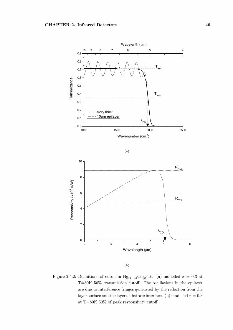
CHAPTER 2. Infrared Detectors 49
1000 1500 2000 25000.0
0.1
0.2
0.3
0.4
0.5
0.6
0.7
0.8
0.910 9 8 7 6 5 4
CO
T50%
TMax
TMax
Tran
smittan
ce
Wavenumber (cm-1)
Very thick 10um epilayer
Wavelenth ( m)
(a)
2 3 4 5 60
2
4
6
8
10
Res
pons
ivity
(x10
5 V/W
)
Wavelength ( m)
RPeak
R50%
CO
(b)
Figure 2.5.2: Definitions of cutoff in Hg(1−x)Cd(x)Te. (a) modelled x = 0.3 at
T=80K 50% transmission cutoff. The oscillations in the epilayer
are due to interference fringes generated by the reflection from the
layer surface and the layer/substrate interface. (b) modelled x = 0.3
at T=80K 50% of peak responsivity cutoff.
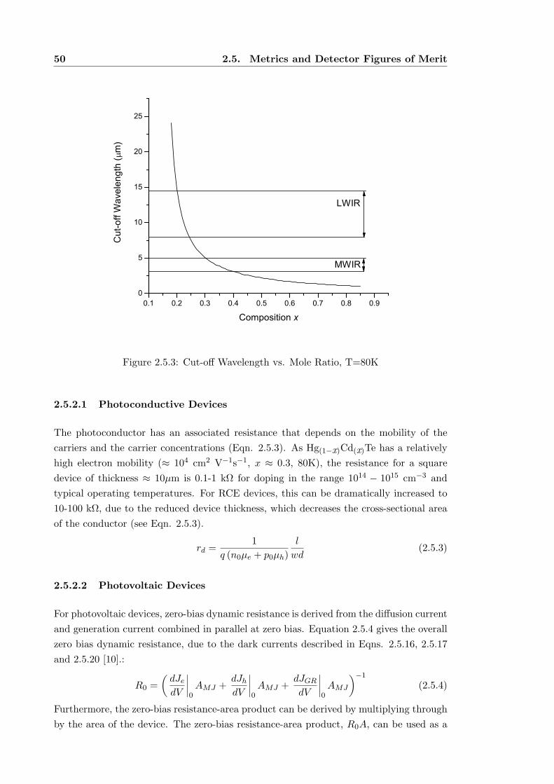
50 2.5. Metrics and Detector Figures of Merit
0.1 0.2 0.3 0.4 0.5 0.6 0.7 0.8 0.90
5
10
15
20
25C
ut-o
ff W
avel
engt
h (
m)
Composition x
LWIR
MWIR
Figure 2.5.3: Cut-off Wavelength vs. Mole Ratio, T=80K
2.5.2.1 Photoconductive Devices
The photoconductor has an associated resistance that depends on the mobility of the
carriers and the carrier concentrations (Eqn. 2.5.3). As Hg(1−x)Cd(x)Te has a relatively
high electron mobility (≈ 104 cm2 V−1s−1, x ≈ 0.3, 80K), the resistance for a square
device of thickness ≈ 10µm is 0.1-1 kΩ for doping in the range 1014 − 1015 cm−3 and
typical operating temperatures. For RCE devices, this can be dramatically increased to
10-100 kΩ, due to the reduced device thickness, which decreases the cross-sectional area
of the conductor (see Eqn. 2.5.3).
rd =1
q (n0µe + p0µh)
l
wd(2.5.3)
2.5.2.2 Photovoltaic Devices
For photovoltaic devices, zero-bias dynamic resistance is derived from the diffusion current
and generation current combined in parallel at zero bias. Equation 2.5.4 gives the overall
zero bias dynamic resistance, due to the dark currents described in Eqns. 2.5.16, 2.5.17
and 2.5.20 [10].:
R0 =
(
dJe
dV
∣
∣
∣
∣
0AMJ +
dJh
dV
∣
∣
∣
∣
0AMJ +
dJGR
dV
∣
∣
∣
∣
0AMJ
)−1
(2.5.4)
Furthermore, the zero-bias resistance-area product can be derived by multiplying through
by the area of the device. The zero-bias resistance-area product, R0A, can be used as a
CHAPTER 2. Infrared Detectors 51
figure of merit to compare detectors, because R0A is directly proportional to signal-to-
noise ratio. A high R0A corresponds to high SNR.
2.5.3 Depletion Region Width
When a p-n junction is formed by bringing an n-type region into intimate contact with a
p-type region there is flow of charge to neutralise the imbalance in charges between the
two regions. This creates a region that is depleted of carriers and is called the depletion
or space-charge region. For an abrupt junction, the width of this region is given by [64]:
Wdep =
√
2εsε0 (Vbi − V ) (NA +ND)
qNDNA(2.5.5)
where:
εs is the dielectric constant,
Vbi is the built in voltage,
V applied voltage, and
NA and ND are the concentration of acceptors and donors, respectively.
For practical material systems, where a region is implanted with dopants or a region is
type converted, then the abrupt junction model is inadequate to describe the width of the
depletion region. Instead a linear approximation to the distribution of dopants is used to
model the changing doping density at the interface [64]:
Wdep =
[
12εsε0 (Vbi − V )
qacg
]1/3
(2.5.6)
where:
Vbi =2kT
qlnacgW0
2ni(2.5.7)
acg =dC
dx
∣
∣
∣
∣
x=xj
(2.5.8)
V is the applied voltage,
W0 is the width of the zero-bias junction, and
acg is the impurity concentration gradient at the junction.
52 2.5. Metrics and Detector Figures of Merit
2.5.4 Responsivity
Responsivity, Rλ, is one of the fundamental figures of merit for a detector. It is defined
as the output voltage or current signal per unit input optical power:
Rλ =Vs, IsP
(2.5.9)
where:
P is the incident optical power impinging on the device,
Vs is the RMS voltage signal (for photoconductive detectors), and
Is is the RMS current signal (for photovoltaic detectors).
Responsivity is actually a function of the modulation frequency of the input optical signal.
For most imaging applications, however, the frequency at which this becomes important
is so high as to not be important. For photoconductive detectors, the low frequency, low
field responsivity is given by [10]:
RV λ =η
lwd
λ
hc
Vbτeff
n0(2.5.10)
This equation indicates that there is a linear relation between the responsivity and the bias
field, however, at high fields, more minority carriers are swept to the high recombination
contacts, resulting in a reduction in the effective bulk lifetime of carriers. This then limits
the responsivity via an effect known as sweepout. Sweepout is only an issue for carriers
with a long lifetime and high mobility.
For photovoltaic detectors the responsivity expression becomes [10]:
RIλ =λ
hcη (λ) q (2.5.11)
where q is the charge of an electron.
2.5.5 Dark Currents and Noise
2.5.5.1 Background Flux
Absorption of thermally generated photons from the background is a random process that
generates noise in the detector. The proportion of the background photon flux that can
potentially generate this noise depends on the field of view of the detector (θ) and the
temperature of the background (Tb), and is given by:
φB = sin2[
θ
2
] ∫ λoff
λon
2πc
λ4(
exp[
hcλkTb
]
− 1)dλ cm−2 s−1 (2.5.12)
The contribution of this noise source to the total noise depends on the detector type, and
will be given in the relevant section below.
CHAPTER 2. Infrared Detectors 53
2.5.5.2 Photoconductive Devices
There are three main noise mechanisms that contribute to the noise voltage for photo-
conductive devices [65]. These are:
• the generation of carriers due to background photon flux, VBG,
• the Johnson noise, VJ , of the device due to the resistance associated with the pho-
toconductor, and
• the thermal generation of carriers within the semiconductor volume, VTh.
The expressions for each of these noise sources are given by [10]:
VBG = 2qrdµeEb
lτeff
√
lwdφBη
df (2.5.13)
VJ =√
4kTrdf (2.5.14)
VTh = 2qrdµeEb
lτeff
√
lwdn0p0
τeff (n0 + p0)f (2.5.15)
The background noise voltage, VBG, is due to photon flux, φB, from the background
generating carriers. It is also dependent on the electron mobility, µe, the effective lifetime,
τeff , the electric bias field, Eb, and the device dimensions.
Johnson noise, VJ is due to blackbody electromagnetic energy in the frequency interval
f within the detector. It is present in every resistive element, and is dependant on
operating temperature, T , and resistance, rd. In conventional photoconductors this is
not the dominant noise source due to the low resistance of such devices; however, in
RCE photoconductive devices, as the absorber layer thickness is two orders of magnitude
thinner than in standard photoconductive detectors, Johnson noise can become dominant,
especially in the presence of surface recombination.
The noise due to random thermal generation and recombination, VTh, is dependent on
the carrier concentrations n0 and p0, as well as the device properties listed above.
2.5.5.3 Photovoltaic Devices
Diffusion is generally the mechanism responsible for noise in the regions outside of the
space-charge region of a p-n junction (noise from the series resistance is also present, but
is usually negligible). Carriers generated in the vicinity of the space-charge region (within
a few diffusion lengths) can diffuse to the edge of the space-charge region and are swept
across the junction. The arrival of carriers to the edge of the depletion region is a random
process and hence a source of noise.
54 2.5. Metrics and Detector Figures of Merit
The current densities due to diffusion of electrons and holes for a device with structure
shown in Fig. 2.2.2 are given by [10]:
Je = qni
NA
De
Le
(
expqV
kT− 1
)
(
1 + βp tanh dLe
βp + tanh dLe
)−1
(2.5.16)
Jh = qni
ND
Dh
Lh
(
expqV
kT− 1
)
(
1 + βe tanh dLh
βe + tanh dLh
)−1
(2.5.17)
βp =SpLe
De(2.5.18)
βe =SnLh
Dh(2.5.19)
where Je and Jh are the diffusion current densities of the minority carriers at the edge
of the depletion region in the p-type and n-type materials, respectively. The diffusion
lengths of p-type and n-type materials are Le and Lh, respectively, and can be replaced
by the distance to the contact (a or d) for a short base diode, while De and Dh are the
minority carrier diffusion coefficients for p-type and n-type material, respectively. The
carrier densities are given by NA, the acceptor density in p-type material, ND, the donor
density in n-type material, and ni is the intrinsic carrier concentration. The surface
recombination velocities Sp and Sn are the recombination velocities at the surface of the
p-type and n-type regions, respectively. The device is biased with voltage V measured
with respect to the n-type side.
Any carriers generated within the depletion region are swept apart and therefore create
a generation noise current across the junction. Other than photogeneration, carriers are
randomly generated by either imperfections within the space-charge region that act as
Shockley-Read-Hall (SRH) generation and recombination centers, or random thermal gen-
eration of electron-hole pairs with SRH generally more important than other generation-
recombination mechanisms. Centers with an energy level close to the intrinsic Fermi level
contribute significantly to the generation current, which leads to a generation current
that follows the temperature dependence of ni [64]. Sah et al. [66] derived an expression
for this noise current by integrating the rate of generation and recombination over the
space-charge region.
CHAPTER 2. Infrared Detectors 55
The expression derived by Sah et al. was modified by Ajisawa et al. [67] to include surface
recombination, and is given by:
JGR = J0GR
2 sinh(
qV2kT
)
(Vbi − V ) qkT
f (b) (2.5.20)
J0GR = J0GRb + J0GRs (2.5.21)
=niWdepkT
τ0Vbi+
4S0niWdepkT
dVbi(2.5.22)
f (b) =1√
1 − b2
arctan
(
b+(
τn
τp
)1/2exp
[
−q(V −Vbi)2kT
]
)
√1 − b2
−arctan
(
b+(
τn
τp
)1/2exp
[
q(V −Vbi)2kT
]
)
√1 − b2
(2.5.23)
b = exp
[−qV2kT
]
cosh
[
Et − Ei
kT+
1
2log
(
τnτp
)]
(2.5.24)
This expression takes into account carriers generated in the volume of the depletion region,
as well as generation where the depletion region intersects the surface for a circular device,
and takes slightly different forms for other device configurations [64]. The generation-
recombination current JGR is dependent on a zero-bias generation-recombination current,
J0GR, the device bias, V , and the built-in voltage, Vbi, as well as the function fgr (b). The
zero-bias g-r current is a function of the current generated in the bulk due to an evenly
distributed concentration of SRH centers and the current generated at the surface due
to SRH centers, which depend on the intrinsic carrier concentration, ni, the depletion
region width, Wdep, the carrier lifetime t0, and the surface recombination velocity where
the depletion region intersects the surface of the device, S0. The function fgr (b) depends
on the carrier lifetimes τn and τp as well as the trap level, Et, and the intrinsic Fermi
level, Ei. There is also a component of dark current due to trap assisted tunnelling which
can dominate the dark current under reverse bias conditions, but as the devices in this
work are tested at zero bias this component is not considered in this work.
2.5.6 Noise Equivalent Power and Detectivity
Noise Equivalent Power (NEP) is a measure of the sensitivity of the device. It corresponds
to a signal-to-noise ratio of one. That is, it is the optical power required to generate a
signal voltage, Vs, that is equal to the noise voltage, Vn, or a signal current, Is, that is
equal to the noise current, Is. Detectivity, D, is simply the reciprocal of NEP.
NEP =Vn
RV λ(W) (2.5.25)
or
NEP =InRIλ
(W) (2.5.26)
D =1
NEP(W−1) (2.5.27)
56 2.5. Metrics and Detector Figures of Merit
2.5.7 Specific Detectivity
Detectivity is not a good figure of merit for comparing different detector structures.
Instead, specific detectivity normalises the detectivity to the measurement bandwidth
and detector area, making it more useful for comparing performance of detectors with
different structures:
D∗ =(Af)1/2
NEP=RI,V λ
I, Vn(Af)1/2 (2.5.28)
where:
D∗ is the specific detectivity (cmHz1/2W−1),
A is the area of detector (cm2), and
f is the electrical measurement bandwidth (Hz).
When the expressions for responsivity and noise voltage for a photoconductor are substi-
tuted into Eqn. 2.5.28, the expression for specific detectivity can be found as [10]:
D∗λ = Rλ
√wlf
√
V 2J + V 2
BG + V 2Th
(2.5.29)
When the noise voltage due to thermal generation of carriers is below the noise voltage
due to generation of carriers from the background photon flux, the device is said to have
background limited performance (BLIP). The Johnson noise voltage is usually below the
other two noise sources for traditional photoconductive detectors, but this is not always
the case for RCE detectors.
Similarly, substituting the expressions for responsivity and noise current for a photovoltaic
detector into Eqn. 2.5.28, the expression for specific detectivity for a photovoltaic detector
becomes [10]:
D∗λ = RIλ
√wlf√
I2n
(2.5.30)
=λ
hcηq
1√
(4kT/R0A) + 2ηq2φB(2.5.31)
For sufficiently high R0A product, the background flux term will dominate the detectivity
expression, and the device is said have background limited performance (BLIP).
2.5.7.1 Specific Detectivity for Background Limited Performance
Optimal performance for IR imaging systems occurs when the device is limited by the
background and not by noise from the detector itself. When a detector fulfills this re-
quirement, it is said to have background limited performance (BLIP). Specific detectivity
of a background limited detector is given solely by the background flux and the efficiency
with which photons are converted to carriers:
D∗ =λ
hc
[
η (λ)
2φB
]1/2
(2.5.32)
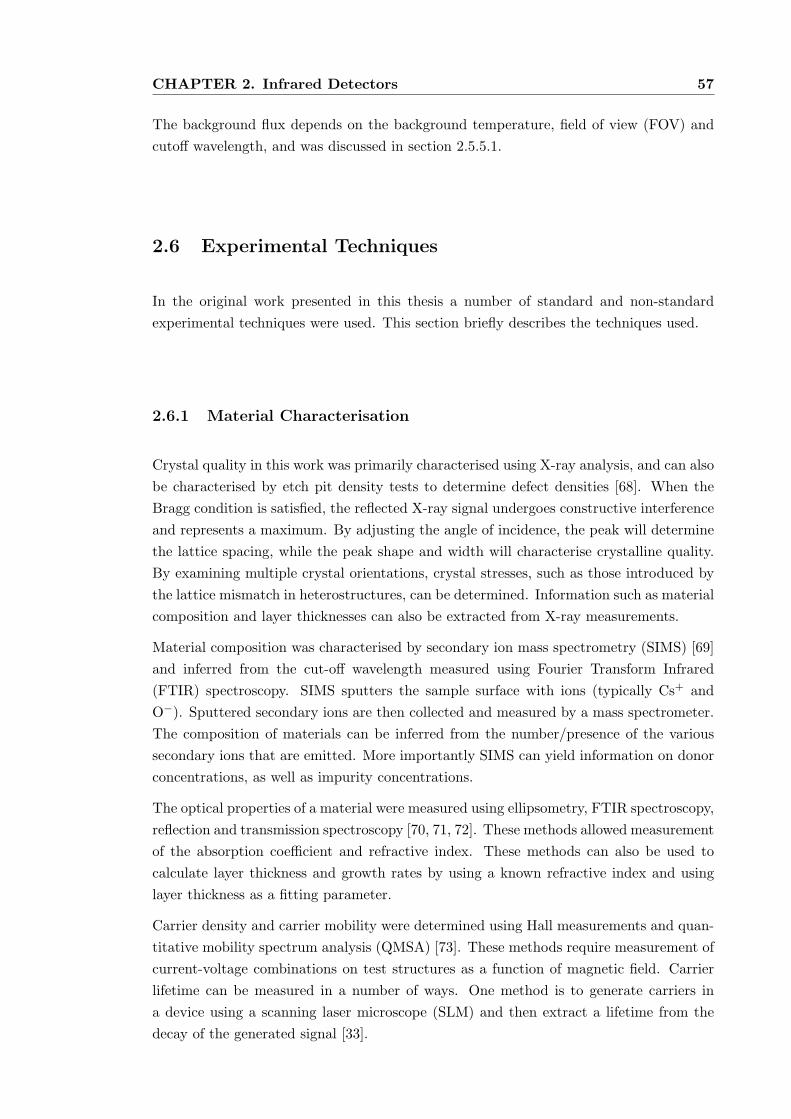
CHAPTER 2. Infrared Detectors 57
The background flux depends on the background temperature, field of view (FOV) and
cutoff wavelength, and was discussed in section 2.5.5.1.
2.6 Experimental Techniques
In the original work presented in this thesis a number of standard and non-standard
experimental techniques were used. This section briefly describes the techniques used.
2.6.1 Material Characterisation
Crystal quality in this work was primarily characterised using X-ray analysis, and can also
be characterised by etch pit density tests to determine defect densities [68]. When the
Bragg condition is satisfied, the reflected X-ray signal undergoes constructive interference
and represents a maximum. By adjusting the angle of incidence, the peak will determine
the lattice spacing, while the peak shape and width will characterise crystalline quality.
By examining multiple crystal orientations, crystal stresses, such as those introduced by
the lattice mismatch in heterostructures, can be determined. Information such as material
composition and layer thicknesses can also be extracted from X-ray measurements.
Material composition was characterised by secondary ion mass spectrometry (SIMS) [69]
and inferred from the cut-off wavelength measured using Fourier Transform Infrared
(FTIR) spectroscopy. SIMS sputters the sample surface with ions (typically Cs+ and
O−). Sputtered secondary ions are then collected and measured by a mass spectrometer.
The composition of materials can be inferred from the number/presence of the various
secondary ions that are emitted. More importantly SIMS can yield information on donor
concentrations, as well as impurity concentrations.
The optical properties of a material were measured using ellipsometry, FTIR spectroscopy,
reflection and transmission spectroscopy [70, 71, 72]. These methods allowed measurement
of the absorption coefficient and refractive index. These methods can also be used to
calculate layer thickness and growth rates by using a known refractive index and using
layer thickness as a fitting parameter.
Carrier density and carrier mobility were determined using Hall measurements and quan-
titative mobility spectrum analysis (QMSA) [73]. These methods require measurement of
current-voltage combinations on test structures as a function of magnetic field. Carrier
lifetime can be measured in a number of ways. One method is to generate carriers in
a device using a scanning laser microscope (SLM) and then extract a lifetime from the
decay of the generated signal [33].
58 2.6. Experimental Techniques
G-R
Tunnelling
Diffusion
Ω
Figure 2.6.1: Photodiode resistance as a function of voltage on a logarithmic
scale, also showing the dominant noise mechanism. Also plotted is
the dark current.
2.6.2 Device Characterisation
Device characterisation methods are concerned primarily with measuring the device per-
formance for bench-marking, and to establish performance limiting mechanisms. The
current-voltage, or I-V, measurement of a device is perhaps one of the most important
measurements. The I-V curve can also be used to extract the dynamic resistance as a
function of bias:1
R=
δI
δV(2.6.1)
For photoconductors with ohmic contacts, the I-V curve is linear, and the dynamic resis-
tance is constant. For photovoltaic devices the I-V curve demonstrates the familiar high
current in forward bias above the diode turn-on voltage, and negligible current below
turn-on and for reverse bias. A typical variation of dynamic resistance with bias for a
photovoltaic device is plotted in Fig. 2.6.1 The mechanisms determining the dynamic
resistance for this device are also indicated. The zero-bias resistance (discussed in section
2.5.2.2) is the dynamic resistance at V = 0.
Performance characterisation includes measurement of device responsivity and noise,
yielding detectivity. Responsivity was measured using a monochromator, and a cali-
brated detector. Device responsivity is determined by comparing measured signal from
the device with the signal from a calibrated detector of known area. Device noise is mea-
sured using a spectrum analyser. However, care must be taken when performing noise
measurements to remove noise sources from the measurement system. Typically, devices

CHAPTER 2. Infrared Detectors 59
are placed in a Faraday cage, and all efforts are made to remove mains power induced
noise sources. Furthermore, noise measurements can be made with the device illuminated
by a 300K background, or with the device in the dark (effectively zero FOV).
The spatial optical response of a device was measured using a scanning laser microscope
(SLM). The spatial photo-response can yield information about which regions of the
device are active optically, and also information about defects due to processing. Another
technique of measurement using a SLM is laser beam induced current (LBIC) which can
be used to characterise diodes [74, 75].

60 2.6. Experimental Techniques
Chapter 3Theory of Resonant-cavity-enhanced
Detectors
3.1 Introduction
This chapter focuses on resonant-cavity-enhanced (RCE) detectors. The development of
resonant-cavity-enhancement and the advantages and disadvantages of RCE detectors are
investigated. The relationships between quantum efficiency, finesse, and absorber thick-
ness are outlined. Modelling of device performance is presented, illustrating the benefits
of RCE detectors. Finally, techniques for fabricating RCE structures are investigated.
3.2 Methods of Improvement
As the adage goes “if it ain’t broke, it doesn’t have enough features.” Research is always
ongoing to expand device function and improve device performance. For infrared pho-
ton detectors device performance focuses on a number of areas, mainly improving the
signal-to-noise performance and also raising the operating temperature to achieve higher
operating temperature (HOT) devices.
For Hg(1−x)Cd(x)Te, historically most of the issues related to improving noise performance
focus on improving material quality, as performance has not been restricted by physical
limits, but by poor material quality. Therefore, most research in the past has investigated
improving contacts, surface passivation and interfaces, and other growth factors such as
reducing dislocation densities. Research into HOT devices has proceeded in three main
areas: Heterostructure devices, multi-junction devices, and more recently resonant-cavity-
enhancement [35, 76, 77, 78, 79, 80].
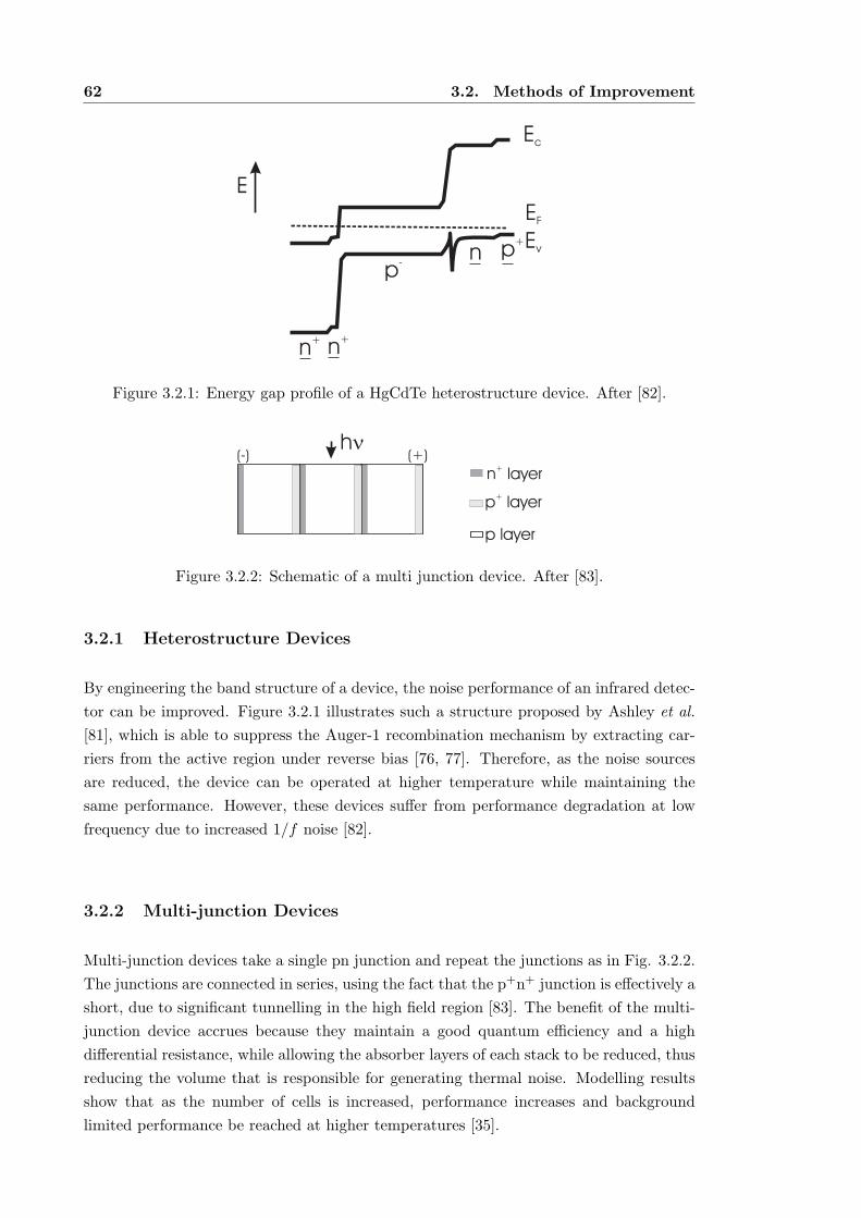
62 3.2. Methods of Improvement
n+ n+
p-n p+Ev
EF
Ec
E
Figure 3.2.1: Energy gap profile of a HgCdTe heterostructure device. After [82].
p layer
p layer+
(+)(-)hn
n layer+
Figure 3.2.2: Schematic of a multi junction device. After [83].
3.2.1 Heterostructure Devices
By engineering the band structure of a device, the noise performance of an infrared detec-
tor can be improved. Figure 3.2.1 illustrates such a structure proposed by Ashley et al.
[81], which is able to suppress the Auger-1 recombination mechanism by extracting car-
riers from the active region under reverse bias [76, 77]. Therefore, as the noise sources
are reduced, the device can be operated at higher temperature while maintaining the
same performance. However, these devices suffer from performance degradation at low
frequency due to increased 1/f noise [82].
3.2.2 Multi-junction Devices
Multi-junction devices take a single pn junction and repeat the junctions as in Fig. 3.2.2.
The junctions are connected in series, using the fact that the p+n+ junction is effectively a
short, due to significant tunnelling in the high field region [83]. The benefit of the multi-
junction device accrues because they maintain a good quantum efficiency and a high
differential resistance, while allowing the absorber layers of each stack to be reduced, thus
reducing the volume that is responsible for generating thermal noise. Modelling results
show that as the number of cells is increased, performance increases and background
limited performance be reached at higher temperatures [35].
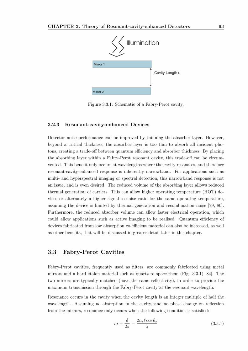
CHAPTER 3. Theory of Resonant-cavity-enhanced Detectors 63
Cavity Length l
Mirror 2
Mirror 1
Illumination
Figure 3.3.1: Schematic of a Fabry-Perot cavity.
3.2.3 Resonant-cavity-enhanced Devices
Detector noise performance can be improved by thinning the absorber layer. However,
beyond a critical thickness, the absorber layer is too thin to absorb all incident pho-
tons, creating a trade-off between quantum efficiency and absorber thickness. By placing
the absorbing layer within a Fabry-Perot resonant cavity, this trade-off can be circum-
vented. This benefit only occurs at wavelengths where the cavity resonates, and therefore
resonant-cavity-enhanced response is inherently narrowband. For applications such as
multi- and hyperspectral imaging or spectral detection, this narrowband response is not
an issue, and is even desired. The reduced volume of the absorbing layer allows reduced
thermal generation of carriers. This can allow higher operating temperature (HOT) de-
vices or alternately a higher signal-to-noise ratio for the same operating temperature,
assuming the device is limited by thermal generation and recombination noise [79, 80].
Furthermore, the reduced absorber volume can allow faster electrical operation, which
could allow applications such as active imaging to be realised. Quantum efficiency of
devices fabricated from low absorption co-efficient material can also be increased, as well
as other benefits, that will be discussed in greater detail later in this chapter.
3.3 Fabry-Perot Cavities
Fabry-Perot cavities, frequently used as filters, are commonly fabricated using metal
mirrors and a hard etalon material such as quartz to space them (Fig. 3.3.1) [84]. The
two mirrors are typically matched (have the same reflectivity), in order to provide the
maximum transmission through the Fabry-Perot cavity at the resonant wavelength.
Resonance occurs in the cavity when the cavity length is an integer multiple of half the
wavelength. Assuming no absorption in the cavity, and no phase change on reflection
from the mirrors, resonance only occurs when the following condition is satisfied:
m =δ
2π=
2nsℓ cos θs
λ(3.3.1)
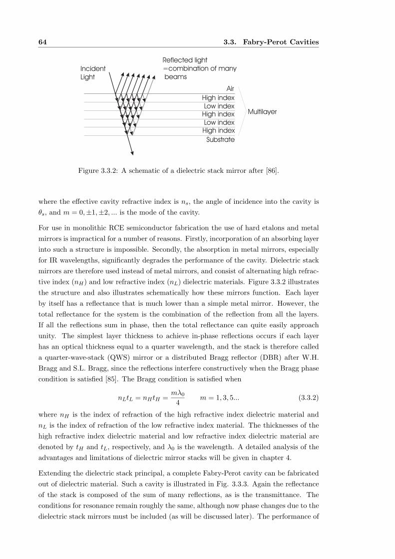
64 3.3. Fabry-Perot Cavities
High indexLow index
High index
High indexLow index
Air
Substrate
IncidentLight
Reflected light=combination of manybeams
Multilayer
Figure 3.3.2: A schematic of a dielectric stack mirror after [86].
where the effective cavity refractive index is ns, the angle of incidence into the cavity is
θs, and m = 0,±1,±2, ... is the mode of the cavity.
For use in monolithic RCE semiconductor fabrication the use of hard etalons and metal
mirrors is impractical for a number of reasons. Firstly, incorporation of an absorbing layer
into such a structure is impossible. Secondly, the absorption in metal mirrors, especially
for IR wavelengths, significantly degrades the performance of the cavity. Dielectric stack
mirrors are therefore used instead of metal mirrors, and consist of alternating high refrac-
tive index (nH) and low refractive index (nL) dielectric materials. Figure 3.3.2 illustrates
the structure and also illustrates schematically how these mirrors function. Each layer
by itself has a reflectance that is much lower than a simple metal mirror. However, the
total reflectance for the system is the combination of the reflection from all the layers.
If all the reflections sum in phase, then the total reflectance can quite easily approach
unity. The simplest layer thickness to achieve in-phase reflections occurs if each layer
has an optical thickness equal to a quarter wavelength, and the stack is therefore called
a quarter-wave-stack (QWS) mirror or a distributed Bragg reflector (DBR) after W.H.
Bragg and S.L. Bragg, since the reflections interfere constructively when the Bragg phase
condition is satisfied [85]. The Bragg condition is satisfied when
nLtL = nHtH =mλ0
4m = 1, 3, 5... (3.3.2)
where nH is the index of refraction of the high refractive index dielectric material and
nL is the index of refraction of the low refractive index material. The thicknesses of the
high refractive index dielectric material and low refractive index dielectric material are
denoted by tH and tL, respectively, and λ0 is the wavelength. A detailed analysis of the
advantages and limitations of dielectric mirror stacks will be given in chapter 4.
Extending the dielectric stack principal, a complete Fabry-Perot cavity can be fabricated
out of dielectric material. Such a cavity is illustrated in Fig. 3.3.3. Again the reflectance
of the stack is composed of the sum of many reflections, as is the transmittance. The
conditions for resonance remain roughly the same, although now phase changes due to the
dielectric stack mirrors must be included (as will be discussed later). The performance of
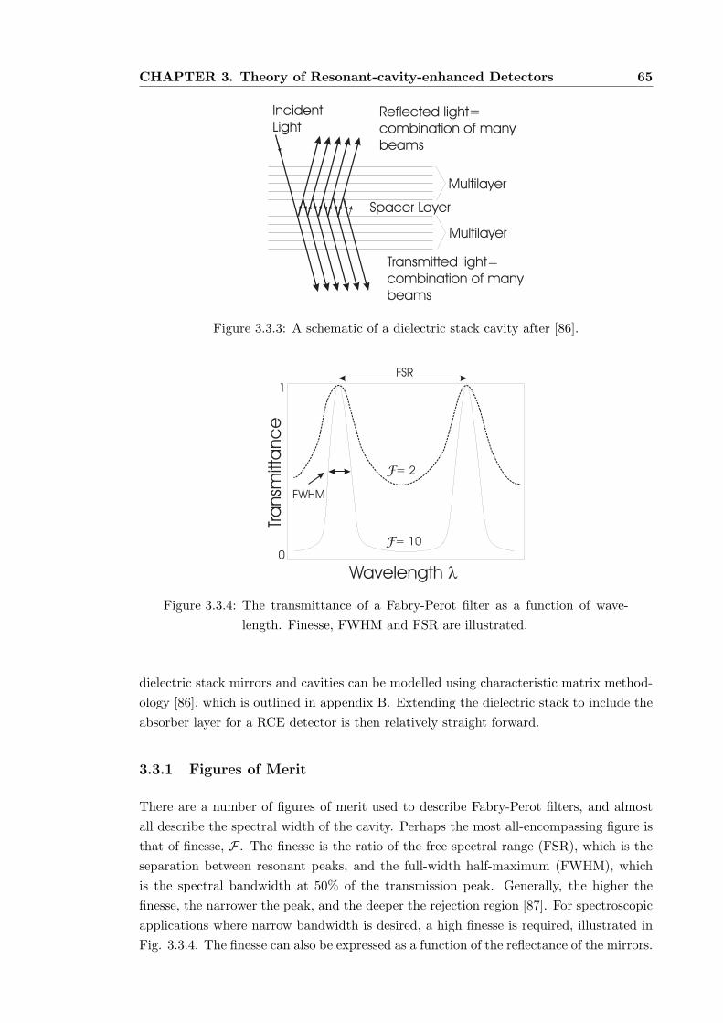
CHAPTER 3. Theory of Resonant-cavity-enhanced Detectors 65
Multilayer
Multilayer
Spacer Layer
Reflected light=combination of manybeams
Transmitted light=combination of manybeams
IncidentLight
Figure 3.3.3: A schematic of a dielectric stack cavity after [86].
Tra
nsm
itta
nc
e
Wavelength l0
1
F= 10
F= 2
FSR
FWHM
Figure 3.3.4: The transmittance of a Fabry-Perot filter as a function of wave-
length. Finesse, FWHM and FSR are illustrated.
dielectric stack mirrors and cavities can be modelled using characteristic matrix method-
ology [86], which is outlined in appendix B. Extending the dielectric stack to include the
absorber layer for a RCE detector is then relatively straight forward.
3.3.1 Figures of Merit
There are a number of figures of merit used to describe Fabry-Perot filters, and almost
all describe the spectral width of the cavity. Perhaps the most all-encompassing figure is
that of finesse, F . The finesse is the ratio of the free spectral range (FSR), which is the
separation between resonant peaks, and the full-width half-maximum (FWHM), which
is the spectral bandwidth at 50% of the transmission peak. Generally, the higher the
finesse, the narrower the peak, and the deeper the rejection region [87]. For spectroscopic
applications where narrow bandwidth is desired, a high finesse is required, illustrated in
Fig. 3.3.4. The finesse can also be expressed as a function of the reflectance of the mirrors.
66 3.3. Fabry-Perot Cavities
For matched mirrors the finesse is given by [84]:
F =π√R
1 −R (3.3.3)
where R is the nominal reflectance of both mirrors.
Another figure of merit is the spectral resolution δλλ . The spectral resolution is also a
measure of FWHM, and is related to the finesse:
λ
δλ= 0.97mF (3.3.4)
where m is the mode of the cavity. Hence, for hyperspectral based detection a spectral
resolution of δλλ ≤ 0.01 implies that a finesse of at least 100 is required for the fundamental
(m = 1) mode. Finally, the quality factor, Q, of the cavity relates the energy within the
cavity to the incident energy, where a higher Q indicates a narrower spectral line width.
The Q of a cavity is related to the finesse by the optical resonator frequency, ν0, and the
mode spacing, νF :
Q =ν0
νFF (3.3.5)
3.3.2 Energy Density
The finesse of a cavity is also a measure of the ratio between the energy within the cavity
to the energy incident, which is given by [88]:
|E|2
|Ein|2=
(∣
∣1 −R21
∣
∣
|1 −R1R2 exp−j (2βℓ+ φ1 + φ2)|2
)
×[
1 +R22 + 2R2 cos [2β (ℓ− z) + φ2]
]
(3.3.6)
β = 2πn/λ0 (3.3.7)
where R1, R2 are the mirror reflectivities, φ1, φ2 are the phase changes on reflection from
the two mirrors, ℓ is the cavity length, z is the position in the cavity, n is the refractive
index of the material in the cavity, and λ0 is the wavelength of incident light. Figure 3.3.5
illustrates the energy density within a cavity that consists of two mirrors, separated by
1.665 µm using the refractive index of CdTe for the cavity, and mirrors of Ge/SiO quarter-
wave-stacks. The cavity is operating in the second order, and the energy density in the
center of the cavity can be seen to be a maximum of approximately 600 times greater than
the incident energy. Wavelengths other than the resonant wavelengths do not exhibit an
increased energy density, and so will not experience any gain in absorption. By placing
an absorbing layer at an anti-node in the energy density function, a vast increase in
absorption is achievable.
The position and number of the nodes and anti-nodes within a cavity depend on the
operating mode. Figure 3.3.6 illustrates the first order mode of an air cavity that is 2
µm long and bounded by Ge/SiO Bragg mirrors centered at 4µm. There are two possible
arrangements for the mode profile, depending on the phase change on reflection occurring
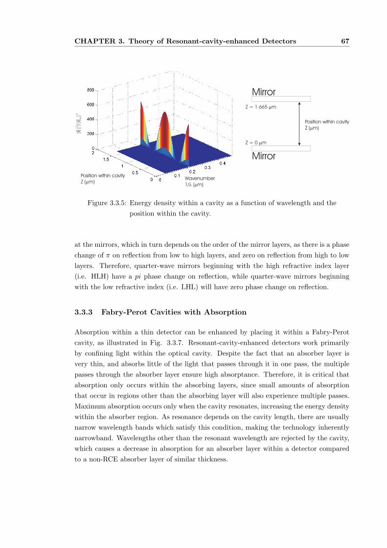
CHAPTER 3. Theory of Resonant-cavity-enhanced Detectors 67
Position within cavityZ ( m)m
Wavenumber1/ ( m)l m
|E|
/|E
|2
2
in
Mirror
Mirror
Z = 0 mm
Z = 1.665 mm
Position within cavityZ ( m)m
Figure 3.3.5: Energy density within a cavity as a function of wavelength and the
position within the cavity.
at the mirrors, which in turn depends on the order of the mirror layers, as there is a phase
change of π on reflection from low to high layers, and zero on reflection from high to low
layers. Therefore, quarter-wave mirrors beginning with the high refractive index layer
(i.e. HLH) have a pi phase change on reflection, while quarter-wave mirrors beginning
with the low refractive index (i.e. LHL) will have zero phase change on reflection.
3.3.3 Fabry-Perot Cavities with Absorption
Absorption within a thin detector can be enhanced by placing it within a Fabry-Perot
cavity, as illustrated in Fig. 3.3.7. Resonant-cavity-enhanced detectors work primarily
by confining light within the optical cavity. Despite the fact that an absorber layer is
very thin, and absorbs little of the light that passes through it in one pass, the multiple
passes through the absorber layer ensure high absorptance. Therefore, it is critical that
absorption only occurs within the absorbing layers, since small amounts of absorption
that occur in regions other than the absorbing layer will also experience multiple passes.
Maximum absorption occurs only when the cavity resonates, increasing the energy density
within the absorber region. As resonance depends on the cavity length, there are usually
narrow wavelength bands which satisfy this condition, making the technology inherently
narrowband. Wavelengths other than the resonant wavelength are rejected by the cavity,
which causes a decrease in absorption for an absorber layer within a detector compared
to a non-RCE absorber layer of similar thickness.
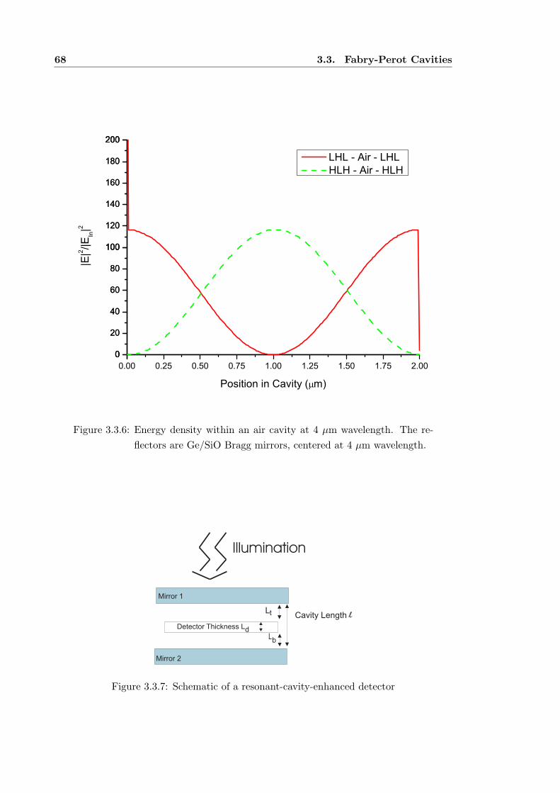
68 3.3. Fabry-Perot Cavities
0
20
40
60
80
100
120
140
160
180
200
0
100
200
0.00 0.25 0.50 0.75 1.00 1.25 1.50 1.75 2.000
20
40
60
80
100
120
140
160
180
200
|E|2 /|
EIn|2
Position in Cavity ( m)
LHL - Air - LHL HLH - Air - HLH
Figure 3.3.6: Energy density within an air cavity at 4 µm wavelength. The re-
flectors are Ge/SiO Bragg mirrors, centered at 4 µm wavelength.
Cavity Length lL
L
t
b
Detector Thickness Ld
Mirror 2
Mirror 1
Illumination
Figure 3.3.7: Schematic of a resonant-cavity-enhanced detector
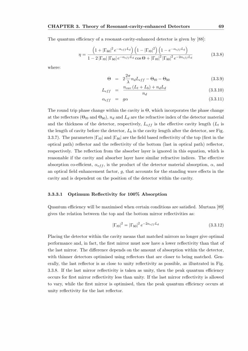
CHAPTER 3. Theory of Resonant-cavity-enhanced Detectors 69
The quantum efficiency of a resonant-cavity-enhanced detector is given by [88]:
η =
(
1 + |Γb0|2 e−αeff Ld
) (
1 − |Γt0|2) (
1 − e−αeff Ld
)
1 − 2 |Γt0| |Γb0| e−αeff Ld cos Θ + |Γt0|2 |Γb0|2 e−2αeff Ld(3.3.8)
where:
Θ = 22π
λndLeff − Θt0 − Θb0 (3.3.9)
Leff =ncav (Lt + Lb) + ndLd
nd(3.3.10)
αeff = gα (3.3.11)
The round trip phase change within the cavity is Θ, which incorporates the phase change
at the reflectors (Θt0 and Θb0), nd and Ld are the refractive index of the detector material
and the thickness of the detector, respectively, Leff is the effective cavity length (Lt is
the length of cavity before the detector, Lb is the cavity length after the detector, see Fig.
3.3.7). The parameters |Γt0| and |Γb0| are the field based reflectivity of the top (first in the
optical path) reflector and the reflectivity of the bottom (last in optical path) reflector,
respectively. The reflection from the absorber layer is ignored in this equation, which is
reasonable if the cavity and absorber layer have similar refractive indices. The effective
absorption co-efficient, αeff , is the product of the detector material absorption, α, and
an optical field enhancement factor, g, that accounts for the standing wave effects in the
cavity and is dependent on the position of the detector within the cavity.
3.3.3.1 Optimum Reflectivity for 100% Absorption
Quantum efficiency will be maximised when certain conditions are satisfied. Murtaza [89]
gives the relation between the top and the bottom mirror reflectivities as:
|Γt0|2 = |Γb0|2 e−2αeff Ld (3.3.12)
Placing the detector within the cavity means that matched mirrors no longer give optimal
performance and, in fact, the first mirror must now have a lower reflectivity than that of
the last mirror. The difference depends on the amount of absorption within the detector,
with thinner detectors optimised using reflectors that are closer to being matched. Gen-
erally, the last reflector is as close to unity reflectivity as possible, as illustrated in Fig.
3.3.8. If the last mirror reflectivity is taken as unity, then the peak quantum efficiency
occurs for first mirror reflectivity less than unity. If the last mirror reflectivity is allowed
to vary, while the first mirror is optimised, then the peak quantum efficiency occurs at
unity reflectivity for the last reflector.
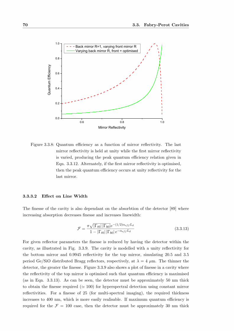
70 3.3. Fabry-Perot Cavities
0.6 0.8 1.00.0
0.2
0.4
0.6
0.8
1.0
Qua
ntum
Effi
cien
cy
Mirror Reflectivity
Back mirror R=1, varying front mirror R Varying back mirror R, front = optimised
Figure 3.3.8: Quantum efficiency as a function of mirror reflectivity. The last
mirror reflectivity is held at unity while the first mirror reflectivity
is varied, producing the peak quantum efficiency relation given in
Eqn. 3.3.12. Alternately, if the first mirror reflectivity is optimised,
then the peak quantum efficiency occurs at unity reflectivity for the
last mirror.
3.3.3.2 Effect on Line Width
The finesse of the cavity is also dependant on the absorbtion of the detector [89] where
increasing absorption decreases finesse and increases linewidth:
F =π√
|Γt0| |Γb0|e−(1/2)αeff Ld
1 − |Γt0| |Γb0| e−αeff Ld(3.3.13)
For given reflector parameters the finesse is reduced by having the detector within the
cavity, as illustrated in Fig. 3.3.9. The cavity is modelled with a unity reflectivity for
the bottom mirror and 0.9945 reflectivity for the top mirror, simulating 20.5 and 3.5
period Ge/SiO distributed Bragg reflectors, respectively, at λ = 4 µm. The thinner the
detector, the greater the finesse. Figure 3.3.9 also shows a plot of finesse in a cavity where
the reflectivity of the top mirror is optimised such that quantum efficiency is maximised
(as in Eqn. 3.3.13). As can be seen, the detector must be approximately 50 nm thick
to obtain the finesse required (≃ 100) for hyperspectral detection using constant mirror
reflectivities. For a finesse of 25 (for multi-spectral imaging), the required thickness
increases to 400 nm, which is more easily realisable. If maximum quantum efficiency is
required for the F = 100 case, then the detector must be approximately 30 nm thick
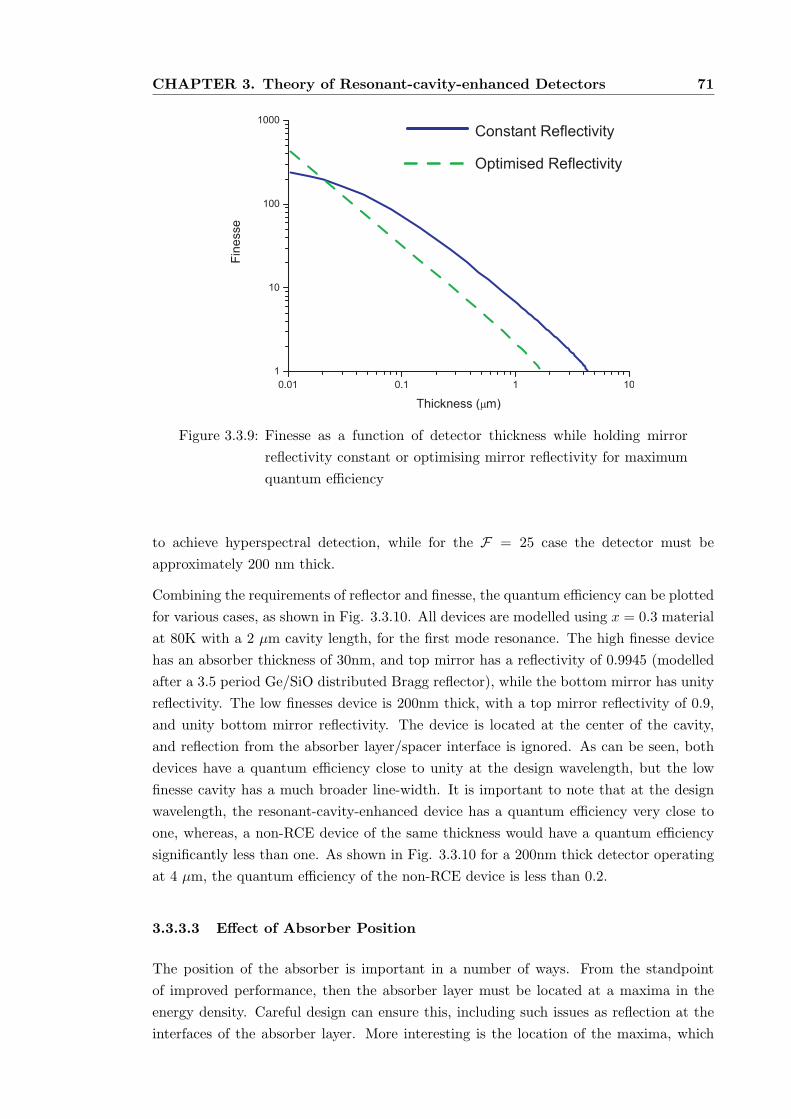
CHAPTER 3. Theory of Resonant-cavity-enhanced Detectors 71
Constant Reflectivity
Optimised Reflectivity
Figure 3.3.9: Finesse as a function of detector thickness while holding mirror
reflectivity constant or optimising mirror reflectivity for maximum
quantum efficiency
to achieve hyperspectral detection, while for the F = 25 case the detector must be
approximately 200 nm thick.
Combining the requirements of reflector and finesse, the quantum efficiency can be plotted
for various cases, as shown in Fig. 3.3.10. All devices are modelled using x = 0.3 material
at 80K with a 2 µm cavity length, for the first mode resonance. The high finesse device
has an absorber thickness of 30nm, and top mirror has a reflectivity of 0.9945 (modelled
after a 3.5 period Ge/SiO distributed Bragg reflector), while the bottom mirror has unity
reflectivity. The low finesses device is 200nm thick, with a top mirror reflectivity of 0.9,
and unity bottom mirror reflectivity. The device is located at the center of the cavity,
and reflection from the absorber layer/spacer interface is ignored. As can be seen, both
devices have a quantum efficiency close to unity at the design wavelength, but the low
finesse cavity has a much broader line-width. It is important to note that at the design
wavelength, the resonant-cavity-enhanced device has a quantum efficiency very close to
one, whereas, a non-RCE device of the same thickness would have a quantum efficiency
significantly less than one. As shown in Fig. 3.3.10 for a 200nm thick detector operating
at 4 µm, the quantum efficiency of the non-RCE device is less than 0.2.
3.3.3.3 Effect of Absorber Position
The position of the absorber is important in a number of ways. From the standpoint
of improved performance, then the absorber layer must be located at a maxima in the
energy density. Careful design can ensure this, including such issues as reflection at the
interfaces of the absorber layer. More interesting is the location of the maxima, which
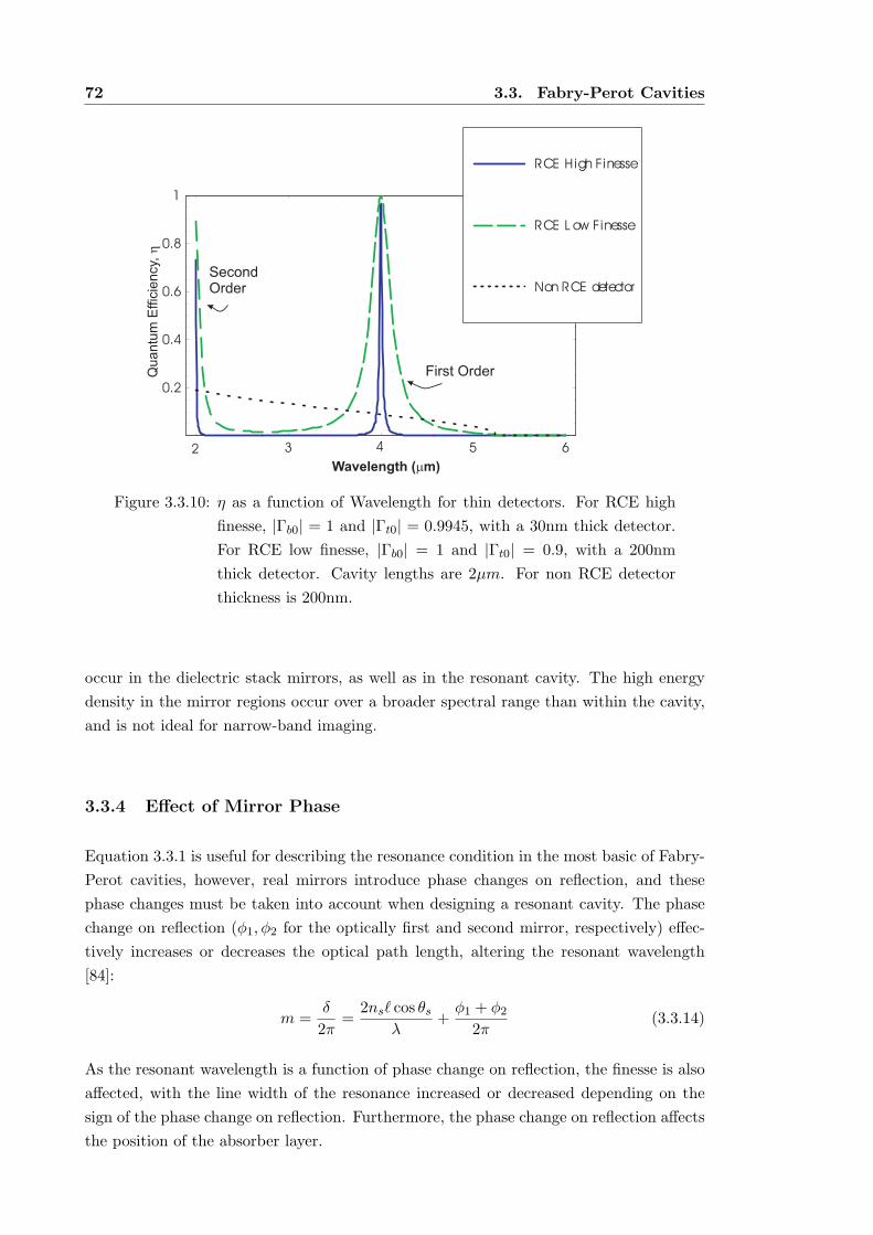
72 3.3. Fabry-Perot Cavities
2 3 4 5 6
Wavelength ( m)m
0.2
0.4
0.6
0.8
1
Quantu
m E
ffic
iency,
h
First Order
SecondOrder
Figure 3.3.10: η as a function of Wavelength for thin detectors. For RCE high
finesse, |Γb0| = 1 and |Γt0| = 0.9945, with a 30nm thick detector.
For RCE low finesse, |Γb0| = 1 and |Γt0| = 0.9, with a 200nm
thick detector. Cavity lengths are 2µm. For non RCE detector
thickness is 200nm.
occur in the dielectric stack mirrors, as well as in the resonant cavity. The high energy
density in the mirror regions occur over a broader spectral range than within the cavity,
and is not ideal for narrow-band imaging.
3.3.4 Effect of Mirror Phase
Equation 3.3.1 is useful for describing the resonance condition in the most basic of Fabry-
Perot cavities, however, real mirrors introduce phase changes on reflection, and these
phase changes must be taken into account when designing a resonant cavity. The phase
change on reflection (φ1, φ2 for the optically first and second mirror, respectively) effec-
tively increases or decreases the optical path length, altering the resonant wavelength
[84]:
m =δ
2π=
2nsℓ cos θs
λ+φ1 + φ2
2π(3.3.14)
As the resonant wavelength is a function of phase change on reflection, the finesse is also
affected, with the line width of the resonance increased or decreased depending on the
sign of the phase change on reflection. Furthermore, the phase change on reflection affects
the position of the absorber layer.
CHAPTER 3. Theory of Resonant-cavity-enhanced Detectors 73
3.4 Examples of RCE Devices
Chin and Chang [90] first proposed the use of a novel device structure which involved
InGaAs absorber layers grown by chemical vapour deposition on AlGaInAs and AlInAs
alternating layers. This first use of resonant-cavity-enhanced detectors was proposed to
overcome the tradeoff between electrical operating bandwidth and quantum efficiency
in optical communication systems without utilising waveguide detectors, which require
edge coupling and suffer from broad spectral response [90, 89]. The bandwidth-efficiency
tradeoff occurs as high-speed detection requires reduced depletion region width to reduce
transit time, as well as reduced area to minimise capacitance, while quantum efficiency
requires adequate detector thickness to ensure all photons are absorbed. The use of
resonant-cavity-enhanced detectors allowed high detector speed, without reducing quan-
tum efficiency. Other material systems targeting communications applications have also
been investigated to determine suitability for RCE detectors [91], for example Ge and Si
absorber layers with various mirror material systems [88].
The RCE detector concept has been extended for use in IR detectors [78, 92, 93, 94] al-
though the importance in reducing detector noise was not immediately recognized. While
Pautrat et al. [78] studied RCE structures primarily for the purpose of RCE vertical cav-
ity surface emitting lasers (VCSELs), they also noted that the structure used for the
VCSELs could be operated as a photoconductor or a photodiode. The spectral pho-
toconductivity measured by Pautrat shows strong agreement with model results, and
resonant detection is observable. Arnold et al. [92] also fabricated RCE detectors using
a lead-chalcogenide absorber layer coupled with a lead-chalcogenide and barium fluoride
spacer and dielectric stack mirror system. Arnold reported peak quantum efficiencies of
32% at a resonant wavelength of 4.4 µm with a FWHM of 0.037 µm, which equates toδλλ = 0.008, which is sufficient for hyperspectral imaging applications. Furthermore, in a
structure similar to Musca et al. [28], Zogg and Arnold [80, 94] have proposed a tuneable
resonant-cavity-enhanced detector.
Sioma et al. [93] proposed a structure for RCE detection in the LWIR window. The
material system was Hg(1−x)Cd(x)Te, and simulated results showed unity absorption at
the design wavelength. Both Sioma and Pautrat note that the resonance condition is
strongly dependant on the angle of incidence of the radiation to be detected.
3.5 Advantages
3.5.1 Speed
For photovoltaic detectors, as absorber layer thickness is reduced the electrical bandwidth
can be increased as it was for optical communications applications of RCE detectors
[90]. This could find applications in range-gated active imaging, where high electrical
bandwidth is a requirement.
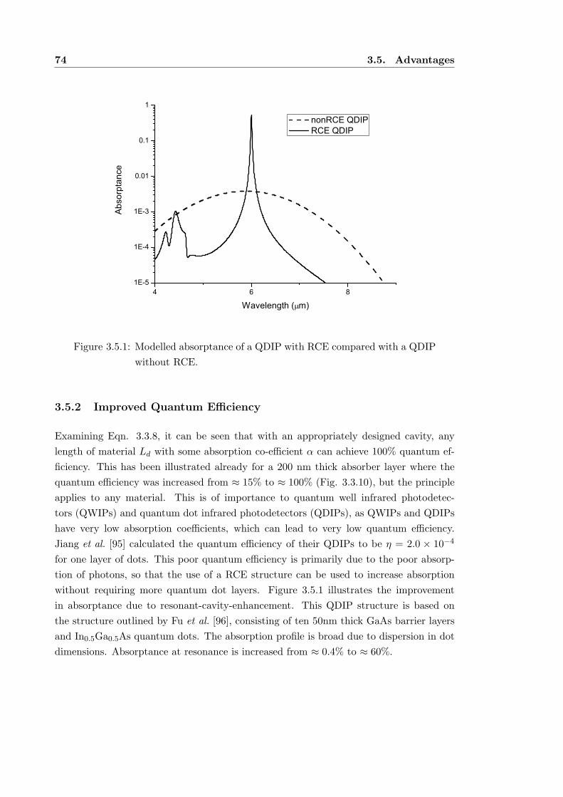
74 3.5. Advantages
4 6 81E-5
1E-4
1E-3
0.01
0.1
1
Abs
orptan
ce
Wavelength ( m)
nonRCE QDIP RCE QDIP
Figure 3.5.1: Modelled absorptance of a QDIP with RCE compared with a QDIP
without RCE.
3.5.2 Improved Quantum Efficiency
Examining Eqn. 3.3.8, it can be seen that with an appropriately designed cavity, any
length of material Ld with some absorption co-efficient α can achieve 100% quantum ef-
ficiency. This has been illustrated already for a 200 nm thick absorber layer where the
quantum efficiency was increased from ≈ 15% to ≈ 100% (Fig. 3.3.10), but the principle
applies to any material. This is of importance to quantum well infrared photodetec-
tors (QWIPs) and quantum dot infrared photodetectors (QDIPs), as QWIPs and QDIPs
have very low absorption coefficients, which can lead to very low quantum efficiency.
Jiang et al. [95] calculated the quantum efficiency of their QDIPs to be η = 2.0 × 10⁻⁴
for one layer of dots. This poor quantum efficiency is primarily due to the poor absorp-
tion of photons, so that the use of a RCE structure can be used to increase absorption
without requiring more quantum dot layers. Figure 3.5.1 illustrates the improvement
in absorptance due to resonant-cavity-enhancement. This QDIP structure is based on
the structure outlined by Fu et al. [96], consisting of ten 50nm thick GaAs barrier layers
and In0.5Ga0.5As quantum dots. The absorption profile is broad due to dispersion in dot
dimensions. Absorptance at resonance is increased from ≈ 0.4% to ≈ 60%.
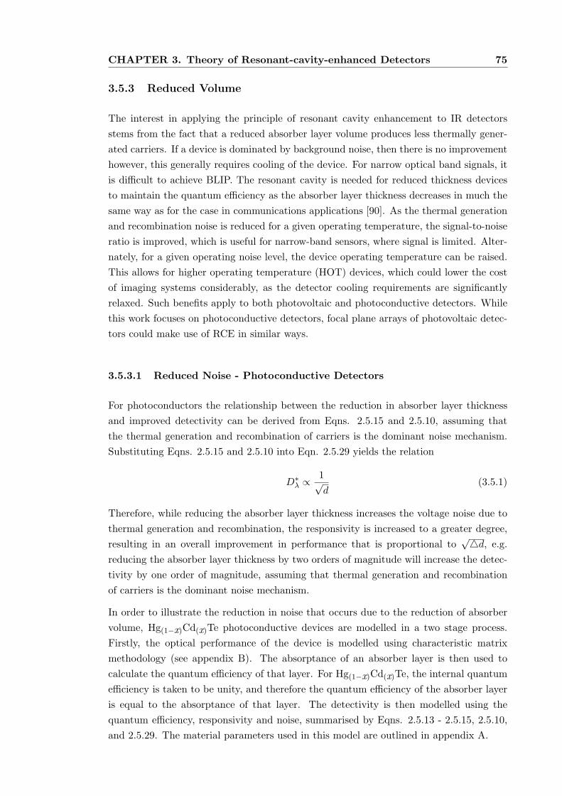
CHAPTER 3. Theory of Resonant-cavity-enhanced Detectors 75
3.5.3 Reduced Volume
The interest in applying the principle of resonant cavity enhancement to IR detectors
stems from the fact that a reduced absorber layer volume produces less thermally gener-
ated carriers. If a device is dominated by background noise, then there is no improvement
however, this generally requires cooling of the device. For narrow optical band signals, it
is difficult to achieve BLIP. The resonant cavity is needed for reduced thickness devices
to maintain the quantum efficiency as the absorber layer thickness decreases in much the
same way as for the case in communications applications [90]. As the thermal generation
and recombination noise is reduced for a given operating temperature, the signal-to-noise
ratio is improved, which is useful for narrow-band sensors, where signal is limited. Alter-
nately, for a given operating noise level, the device operating temperature can be raised.
This allows for higher operating temperature (HOT) devices, which could lower the cost
of imaging systems considerably, as the detector cooling requirements are significantly
relaxed. Such benefits apply to both photovoltaic and photoconductive detectors. While
this work focuses on photoconductive detectors, focal plane arrays of photovoltaic detec-
tors could make use of RCE in similar ways.
3.5.3.1 Reduced Noise - Photoconductive Detectors
For photoconductors the relationship between the reduction in absorber layer thickness
and improved detectivity can be derived from Eqns. 2.5.15 and 2.5.10, assuming that
the thermal generation and recombination of carriers is the dominant noise mechanism.
Substituting Eqns. 2.5.15 and 2.5.10 into Eqn. 2.5.29 yields the relation
D∗λ ∝ 1√
d(3.5.1)
Therefore, while reducing the absorber layer thickness increases the voltage noise due to
thermal generation and recombination, the responsivity is increased to a greater degree,
resulting in an overall improvement in performance that is proportional to√d, e.g.
reducing the absorber layer thickness by two orders of magnitude will increase the detec-
tivity by one order of magnitude, assuming that thermal generation and recombination
of carriers is the dominant noise mechanism.
In order to illustrate the reduction in noise that occurs due to the reduction of absorber
volume, Hg(1−x)Cd(x)Te photoconductive devices are modelled in a two stage process.
Firstly, the optical performance of the device is modelled using characteristic matrix
methodology (see appendix B). The absorptance of an absorber layer is then used to
calculate the quantum efficiency of that layer. For Hg(1−x)Cd(x)Te, the internal quantum
efficiency is taken to be unity, and therefore the quantum efficiency of the absorber layer
is equal to the absorptance of that layer. The detectivity is then modelled using the
quantum efficiency, responsivity and noise, summarised by Eqns. 2.5.13 - 2.5.15, 2.5.10,
and 2.5.29. The material parameters used in this model are outlined in appendix A.
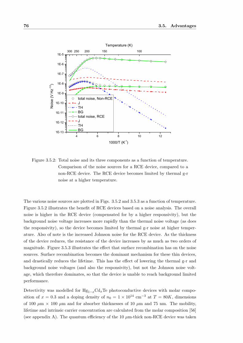
76 3.5. Advantages
4 6 8 10 121E-13
1E-12
1E-11
1E-10
1E-9
1E-8
1E-7
1E-6
1E-5300 250 200 150 100
Noi
se (V
Hz-1
/2)
1000/T (K-1)
total noise, Non-RCE J TH BG total noise, RCE J TH BG
Temperature (K)
Figure 3.5.2: Total noise and its three components as a function of temperature.
Comparison of the noise sources for a RCE device, compared to a
non-RCE device. The RCE device becomes limited by thermal g-r
noise at a higher temperature.
The various noise sources are plotted in Figs. 3.5.2 and 3.5.3 as a function of temperature.
Figure 3.5.2 illustrates the benefit of RCE devices based on a noise analysis. The overall
noise is higher in the RCE device (compensated for by a higher responsivity), but the
background noise voltage increases more rapidly than the thermal noise voltage (as does
the responsivity), so the device becomes limited by thermal g-r noise at higher temper-
ature. Also of note is the increased Johnson noise for the RCE device. As the thickness
of the device reduces, the resistance of the device increases by as much as two orders of
magnitude. Figure 3.5.3 illustrates the effect that surface recombination has on the noise
sources. Surface recombination becomes the dominant mechanism for these thin devices,
and drastically reduces the lifetime. This has the effect of lowering the thermal g-r and
background noise voltages (and also the responsivity), but not the Johnson noise volt-
age, which therefore dominates, so that the device is unable to reach background limited
performance.
Detectivity was modelled for Hg1−xCdxTe photoconductive devices with molar compo-
sition of x = 0.3 and a doping density of n0 = 1 × 1014 cm−3 at T = 80K, dimensions
of 100 µm × 100 µm and for absorber thicknesses of 10 µm and 75 nm. The mobility,
lifetime and intrinsic carrier concentration are calculated from the molar composition [56]
(see appendix A). The quantum efficiency of the 10 µm-thick non-RCE device was taken
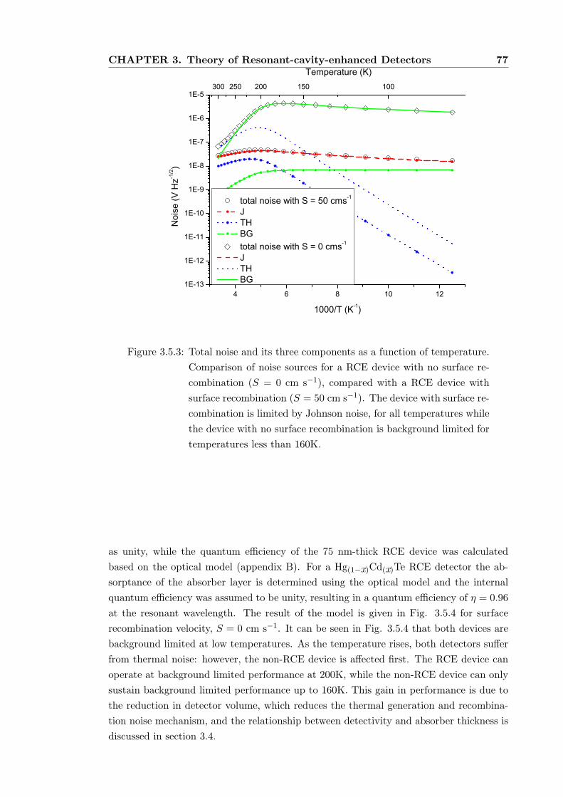
CHAPTER 3. Theory of Resonant-cavity-enhanced Detectors 77
4 6 8 10 121E-13
1E-12
1E-11
1E-10
1E-9
1E-8
1E-7
1E-6
1E-5300 250 200 150 100
Noi
se (V
Hz-1
/2)
1000/T (K-1)
total noise with S = 50 cms-1
J TH BG total noise with S = 0 cms-1
J TH BG
Temperature (K)
Figure 3.5.3: Total noise and its three components as a function of temperature.
Comparison of noise sources for a RCE device with no surface re-
combination (S = 0 cm s−1), compared with a RCE device with
surface recombination (S = 50 cm s−1). The device with surface re-
combination is limited by Johnson noise, for all temperatures while
the device with no surface recombination is background limited for
temperatures less than 160K.
as unity, while the quantum efficiency of the 75 nm-thick RCE device was calculated
based on the optical model (appendix B). For a Hg(1−x)Cd(x)Te RCE detector the ab-
sorptance of the absorber layer is determined using the optical model and the internal
quantum efficiency was assumed to be unity, resulting in a quantum efficiency of η = 0.96
at the resonant wavelength. The result of the model is given in Fig. 3.5.4 for surface
recombination velocity, S = 0 cm s−1. It can be seen in Fig. 3.5.4 that both devices are
background limited at low temperatures. As the temperature rises, both detectors suffer
from thermal noise: however, the non-RCE device is affected first. The RCE device can
operate at background limited performance at 200K, while the non-RCE device can only
sustain background limited performance up to 160K. This gain in performance is due to
the reduction in detector volume, which reduces the thermal generation and recombina-
tion noise mechanism, and the relationship between detectivity and absorber thickness is
discussed in section 3.4.
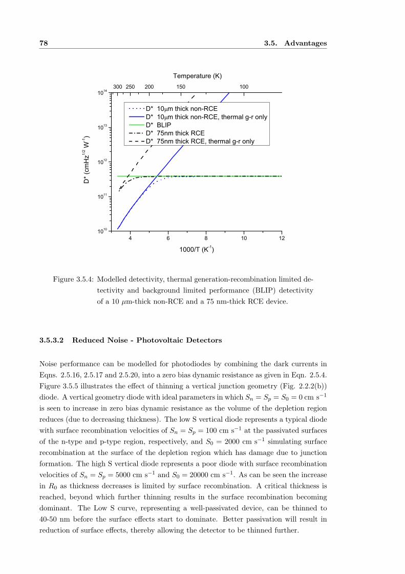
78 3.5. Advantages
4 6 8 10 121010
1011
1012
1013
1014300 250 200 150 100
D*
(cm
Hz1/
2 W-1)
1000/T (K-1)
D* 10 m thick non-RCE D* 10 m thick non-RCE, thermal g-r only D* BLIP D* 75nm thick RCE D* 75nm thick RCE, thermal g-r only
Temperature (K)
Figure 3.5.4: Modelled detectivity, thermal generation-recombination limited de-
tectivity and background limited performance (BLIP) detectivity
of a 10 µm-thick non-RCE and a 75 nm-thick RCE device.
3.5.3.2 Reduced Noise - Photovoltaic Detectors
Noise performance can be modelled for photodiodes by combining the dark currents in
Eqns. 2.5.16, 2.5.17 and 2.5.20, into a zero bias dynamic resistance as given in Eqn. 2.5.4.
Figure 3.5.5 illustrates the effect of thinning a vertical junction geometry (Fig. 2.2.2(b))
diode. A vertical geometry diode with ideal parameters in which Sn = Sp = S0 = 0 cm s−1
is seen to increase in zero bias dynamic resistance as the volume of the depletion region
reduces (due to decreasing thickness). The low S vertical diode represents a typical diode
with surface recombination velocities of Sn = Sp = 100 cm s−1 at the passivated surfaces
of the n-type and p-type region, respectively, and S0 = 2000 cm s−1 simulating surface
recombination at the surface of the depletion region which has damage due to junction
formation. The high S vertical diode represents a poor diode with surface recombination
velocities of Sn = Sp = 5000 cm s−1 and S0 = 20000 cm s−1. As can be seen the increase
in R0 as thickness decreases is limited by surface recombination. A critical thickness is
reached, beyond which further thinning results in the surface recombination becoming
dominant. The Low S curve, representing a well-passivated device, can be thinned to
40-50 nm before the surface effects start to dominate. Better passivation will result in
reduction of surface effects, thereby allowing the detector to be thinned further.
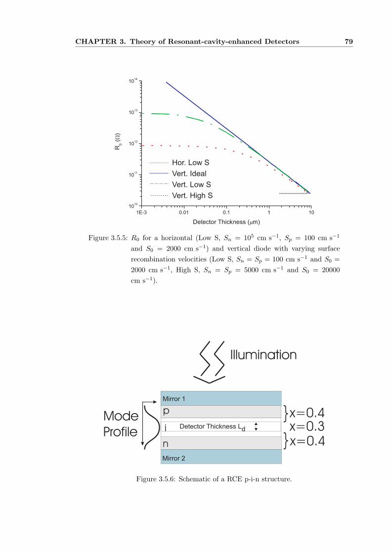
CHAPTER 3. Theory of Resonant-cavity-enhanced Detectors 79
Hor. Low S
Vert. Ideal
Vert. Low S
Vert. High S
Figure 3.5.5: R0 for a horizontal (Low S, Sn = 105 cm s−1, Sp = 100 cm s−1
and S0 = 2000 cm s−1) and vertical diode with varying surface
recombination velocities (Low S, Sn = Sp = 100 cm s−1 and S0 =
2000 cm s−1, High S, Sn = Sp = 5000 cm s−1 and S0 = 20000
cm s−1).
Mirror 2
Mirror 1
Illumination
ModeProfile
Detector Thickness Ld
p
i
n
x=0.4
x=0.4x=0.3
Figure 3.5.6: Schematic of a RCE p-i-n structure.
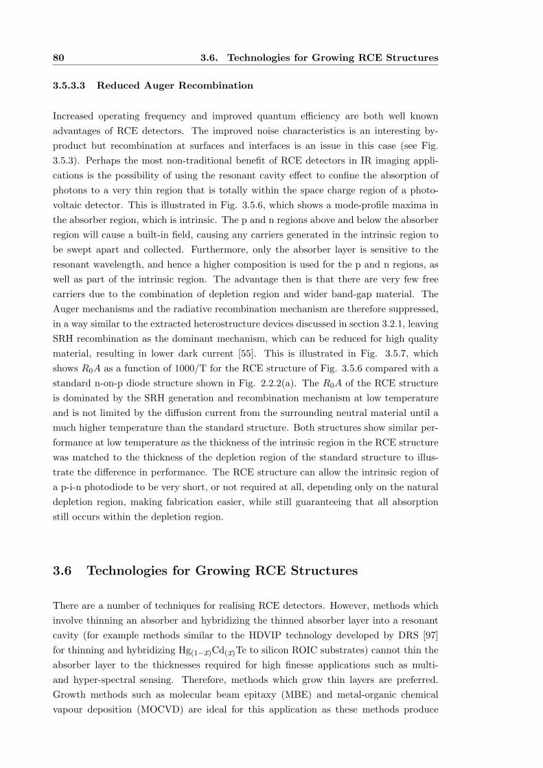
80 3.6. Technologies for Growing RCE Structures
3.5.3.3 Reduced Auger Recombination
Increased operating frequency and improved quantum efficiency are both well known
advantages of RCE detectors. The improved noise characteristics is an interesting by-
product but recombination at surfaces and interfaces is an issue in this case (see Fig.
3.5.3). Perhaps the most non-traditional benefit of RCE detectors in IR imaging appli-
cations is the possibility of using the resonant cavity effect to confine the absorption of
photons to a very thin region that is totally within the space charge region of a photo-
voltaic detector. This is illustrated in Fig. 3.5.6, which shows a mode-profile maxima in
the absorber region, which is intrinsic. The p and n regions above and below the absorber
region will cause a built-in field, causing any carriers generated in the intrinsic region to
be swept apart and collected. Furthermore, only the absorber layer is sensitive to the
resonant wavelength, and hence a higher composition is used for the p and n regions, as
well as part of the intrinsic region. The advantage then is that there are very few free
carriers due to the combination of depletion region and wider band-gap material. The
Auger mechanisms and the radiative recombination mechanism are therefore suppressed,
in a way similar to the extracted heterostructure devices discussed in section 3.2.1, leaving
SRH recombination as the dominant mechanism, which can be reduced for high quality
material, resulting in lower dark current [55]. This is illustrated in Fig. 3.5.7, which
shows R0A as a function of 1000/T for the RCE structure of Fig. 3.5.6 compared with a
standard n-on-p diode structure shown in Fig. 2.2.2(a). The R0A of the RCE structure
is dominated by the SRH generation and recombination mechanism at low temperature
and is not limited by the diffusion current from the surrounding neutral material until a
much higher temperature than the standard structure. Both structures show similar per-
formance at low temperature as the thickness of the intrinsic region in the RCE structure
was matched to the thickness of the depletion region of the standard structure to illus-
trate the difference in performance. The RCE structure can allow the intrinsic region of
a p-i-n photodiode to be very short, or not required at all, depending only on the natural
depletion region, making fabrication easier, while still guaranteeing that all absorption
still occurs within the depletion region.
3.6 Technologies for Growing RCE Structures
There are a number of techniques for realising RCE detectors. However, methods which
involve thinning an absorber and hybridizing the thinned absorber layer into a resonant
cavity (for example methods similar to the HDVIP technology developed by DRS [97]
for thinning and hybridizing Hg(1−x)Cd(x)Te to silicon ROIC substrates) cannot thin the
absorber layer to the thicknesses required for high finesse applications such as multi-
and hyper-spectral sensing. Therefore, methods which grow thin layers are preferred.
Growth methods such as molecular beam epitaxy (MBE) and metal-organic chemical
vapour deposition (MOCVD) are ideal for this application as these methods produce
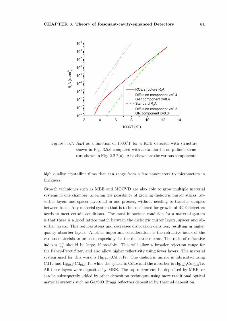
CHAPTER 3. Theory of Resonant-cavity-enhanced Detectors 81
2 4 6 8 10 12 14100
101
102
103
104
105
106
107
108
109
R0A
( c
m2 )
1000/T (K-1)
RCE structure R0A
Diffusion component x=0.4 G-R component x=0.4 Standard R
0A
Diffusion component x=0.3 GR component x=0.3
Figure 3.5.7: R0A as a function of 1000/T for a RCE detector with structure
shown in Fig. 3.5.6 compared with a standard n-on-p diode struc-
ture shown in Fig. 2.2.2(a). Also shown are the various components.
high quality crystalline films that can range from a few nanometers to micrometers in
thickness.
Growth techniques such as MBE and MOCVD are also able to grow multiple material
systems in one chamber, allowing the possibility of growing dielectric mirror stacks, ab-
sorber layers and spacer layers all in one process, without needing to transfer samples
between tools. Any material system that is to be considered for growth of RCE detectors
needs to meet certain conditions. The most important condition for a material system
is that there is a good lattice match between the dielectric mirror layers, spacer and ab-
sorber layers. This reduces stress and decreases dislocation densities, resulting in higher
quality absorber layers. Another important consideration, is the refractive index of the
various materials to be used, especially for the dielectric mirror. The ratio of refractive
indexes nH
nLshould be large, if possible. This will allow a broader rejection range for
the Fabry-Perot filter, and also allow higher reflectivity using fewer layers. The material
system used for this work is Hg(1−x)Cd(x)Te. The dielectric mirror is fabricated using
CdTe and Hg(0.6)Cd(0.4)Te, while the spacer is CdTe and the absorber is Hg(0.7)Cd(0.3)Te.
All these layers were deposited by MBE. The top mirror can be deposited by MBE, or
can be subsequently added by other deposition techniques using more traditional optical
material systems such as Ge/SiO Bragg reflectors deposited by thermal deposition.

82 3.6. Technologies for Growing RCE Structures
Chapter 4Staggered Dielectric Mirrors
4.1 Introduction
In resonant-cavity-enhanced (RCE) structures the mirrors are a critical part of the design.
Generally, for IR applications the absorption in metal mirrors precludes their use for
Fabry-Perot cavities, and therefore dielectric mirrors are required. Figure 4.1.1 shows the
proposed RCE structure that will be realised in this work, indicating the absorber layer
between two mirrors. As the absorber is to be grown by MBE, one of the mirrors will
also need to be grown by MBE as a lattice matched template and to simplify fabrication,
as illustrated by the Hg(0.6)Cd(0.4)Te/CdTe mirror (mirror 1). For such RCE designs
in which the critical absorber layer is grown on top of one of the mirrors, the mirror
design becomes particularly important and must meet a number of requirements that are
sometimes mutually exclusive: the reflectivity for the mirror must be high enough to allow
resonance, and the spectral bandwidth of the reflector must be broad enough to cover
the window for the required application. The mirror must also provide a good crystalline
surface on which to grow the absorber layer. The material system needed to achieve a high
quality crystalline absorber determines the refractive indices available for the dielectric
mirrors, which can have implications for spectral bandwidth and reflectivity. This chapter
investigates the design of mirrors fabricated from the HgCdTe/CdTe material system,
their growth and also investigates how such mirrors will survive subsequent processing
steps.
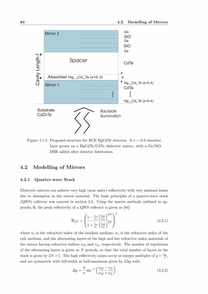
84 4.2. Modelling of Mirrors
Cavity L
ength
l
SubstrateCdZnTe
BacksideIllumination
Absorber Hg Cd Te (x=0.3)(1-x) (x) d
Mirror 2
Mirror 1
SiOGe
SiO
Ge
CdTe
CdTeSpacer
Ge
Hg Cd Te(1-x) (x) (x=0.4)
Hg Cd Te(1-x) (x) (x=0.4)
Figure 4.1.1: Proposed structure for RCE HgCdTe detector. A x = 0.3 absorber
layer grown on a HgCdTe/CdTe dielectric mirror, with a Ge/SiO
DBR added after detector fabrication.
4.2 Modelling of Mirrors
4.2.1 Quarter-wave Stack
Dielectric mirrors can achieve very high (near unity) reflectivity with very minimal losses
due to absorption in the mirror material. The basic principles of a quarter-wave stack
(QWS) reflector was covered in section 3.3. Using the matrix methods outlined in ap-
pendix B, the peak reflectivity of a QWS reflector is given as [84]:
R2N =
1 − ns
ni
(
nH
nL
)2N
1 + ns
ni
(
nH
nL
)2N
2
(4.2.1)
where ni is the refractive index of the incident medium, ns is the refractive index of the
exit medium, and the alternating layers of the high and low refractive index materials of
the mirror having refractive indices nH and nL, respectively. The number of repetitions
of the alternating layers is given as N periods, so that the total number of layers in the
stack is given by 2N +1. The high reflectivity zones occur at integer multiples of g = λ0
λ ,
and are symmetric with full-width at half-maximum given by 2∆g with
∆g =2
πsin−1
(
nH − nL
nH + nL
)
(4.2.2)
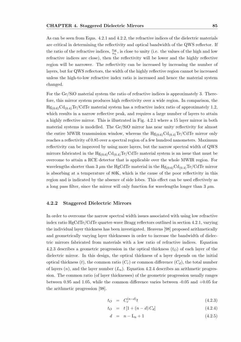
CHAPTER 4. Staggered Dielectric Mirrors 85
As can be seen from Eqns. 4.2.1 and 4.2.2, the refractive indices of the dielectric materials
are critical in determining the reflectivity and optical bandwidth of the QWS reflector. If
the ratio of the refractive indices, nH
nL, is close to unity (i.e. the values of the high and low
refractive indices are close), then the reflectivity will be lower and the highly reflective
region will be narrower. The reflectivity can be increased by increasing the number of
layers, but for QWS reflectors, the width of the highly reflective region cannot be increased
unless the high-to-low refractive index ratio is increased and hence the material system
changed.
For the Ge/SiO material system the ratio of refractive indices is approximately 3. There-
fore, this mirror system produces high reflectivity over a wide region. In comparison, the
Hg(0.6)Cd(0.4)Te/CdTe material system has a refractive index ratio of approximately 1.2,
which results in a narrow reflective peak, and requires a large number of layers to attain
a highly reflective mirror. This is illustrated in Fig. 4.2.1 where a 15 layer mirror in both
material systems is modelled. The Ge/SiO mirror has near unity reflectivity for almost
the entire MWIR transmission window, whereas the Hg(0.6)Cd(0.4)Te/CdTe mirror only
reaches a reflectivity of 0.85 over a spectral region of a few hundred nanometers. Maximum
reflectivity can be improved by using more layers, but the narrow spectral width of QWS
mirrors fabricated in the Hg(0.6)Cd(0.4)Te/CdTe material system is an issue that must be
overcome to attain a RCE detector that is applicable over the whole MWIR region. For
wavelengths shorter than 3 µm the HgCdTe material in the Hg(0.6)Cd(0.4)Te/CdTe mirror
is absorbing at a temperature of 80K, which is the cause of the poor reflectivity in this
region and is indicated by the absence of side lobes. This effect can be used effectively as
a long pass filter, since the mirror will only function for wavelengths longer than 3 µm.
4.2.2 Staggered Dielectric Mirrors
In order to overcome the narrow spectral width issues associated with using low refractive
index ratio HgCdTe/CdTe quarter-wave Bragg reflectors outlined in section 4.2.1, varying
the individual layer thickness has been investigated. Heavens [98] proposed arithmetically
and geometrically varying layer thicknesses in order to increase the bandwidth of dielec-
tric mirrors fabricated from materials with a low ratio of refractive indices. Equation
4.2.3 describes a geometric progression in the optical thickness (tO) of each layer of the
dielectric mirror. In this design, the optical thickness of a layer depends on the initial
optical thickness (t), the common ratio (Cr) or common difference (Cd), the total number
of layers (n), and the layer number (Ln). Equation 4.2.4 describes an arithmetic progres-
sion. The common ratio (of layer thicknesses) of the geometric progression usually ranges
between 0.95 and 1.05, while the common difference varies between -0.05 and +0.05 for
the arithmetic progression [98].
tO = C(n−d)r t (4.2.3)
tO = t [1 + (n− d)Cd] (4.2.4)
d = n− Ln + 1 (4.2.5)
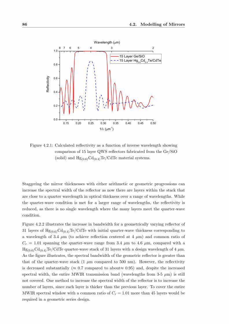
86 4.2. Modelling of Mirrors
0.15 0.20 0.25 0.30 0.35 0.40 0.45 0.500.0
0.2
0.4
0.6
0.8
1.08 7 6 5 4 3 2
Reflectivity
1/ ( m-1)
15 Layer Ge/SiO 15 Layer Hg
0.6Cd
0.4Te/CdTe
Wavelength ( m)
Figure 4.2.1: Calculated reflectivity as a function of inverse wavelength showing
comparison of 15 layer QWS reflectors fabricated from the Ge/SiO
(solid) and Hg(0.6)Cd(0.4)Te/CdTe material systems.
Staggering the mirror thicknesses with either arithmetic or geometric progressions can
increase the spectral width of the reflector as now there are layers within the stack that
are close to a quarter wavelength in optical thickness over a range of wavelengths. While
the quarter-wave condition is met for a larger range of wavelengths, the reflectivity is
reduced, as there is no single wavelength where the many layers meet the quarter-wave
condition.
Figure 4.2.2 illustrates the increase in bandwidth for a geometrically varying reflector of
31 layers of Hg(0.6)Cd(0.4)Te/CdTe with initial quarter-wave thickness corresponding to
a wavelength of 3.4 µm (to achieve reflection centered at 4 µm) and common ratio of
Cr = 1.01 spanning the quarter-wave range from 3.4 µm to 4.6 µm, compared with a
Hg(0.6)Cd(0.4)Te/CdTe quarter-wave stack of 31 layers with a design wavelength of 4 µm.
As the figure illustrates, the spectral bandwidth of the geometric reflector is greater than
that of the quarter-wave stack (1 µm compared to 500 nm). However, the reflectivity
is decreased substantially (≈ 0.7 compared to about≈ 0.95) and, despite the increased
spectral width, the entire MWIR transmission band (wavelengths from 3-5 µm) is still
not covered. One method to increase the spectral width of the reflector is to increase the
number of layers, since each layer is thicker than the previous layer. To cover the entire
MWIR spectral window with a common ratio of Cr = 1.01 more than 45 layers would be
required in a geometric series design.
CHAPTER 4. Staggered Dielectric Mirrors 87
0.15 0.20 0.25 0.30 0.35 0.40 0.45 0.500.0
0.2
0.4
0.6
0.8
1.08 7 6 5 4 3 2
Reflectivity
1/ ( m-1)
31 Layer QWS 31 Layer Geometric stack
Wavelength ( m)
Figure 4.2.2: Reflectivity as a function of inverse wavelength, solid line: Quar-
ter wave stack using Hg(0.6)Cd(0.4)Te/CdTe, 31 layers. Dashed
line: Asymmetric geometrically varying dielectric stack mirror us-
ing Hg(0.6)Cd(0.4)Te/CdTe, 31 layers, initial thickness of 3.4 µm,
common ratio Cr = 1.01.
Rather than increase the number of layers to increase the spectral width, the common ratio
(difference) could be increased. As the common ratio (difference) increases, each layer in
the stack increases in thickness at a faster rate. This further reduces reflectivity, as there
are greater spectral ranges that are not near a quarter-wave layer thickness in the stack.
This is illustrated in Fig. 4.2.3. Using a geometrically varying Hg(1−x)Cd(x)Te/CdTe
mirror with a common ratio of Cr = 1.01, the wavelength range from approximately 3.6
to 4.4 µm can be covered. Using a common ratio of Cr = 1.02 the wavelength range
from approximately 3.2 to 5 µm can be covered. It should also be noted that a higher
common ratio also results in more fluctuations in reflectivity across the spectral band,
which is generally not desired. For the Hg(1−x)Cd(x)Te/CdTe material system a common
ratio higher than Cr = 1.02 results in a rapid decay in reflectivity and a rapid increase in
fluctuations in reflectivity across the spectral band. This essentially means that common
ratios are restricted to below 1.02 for this material system.
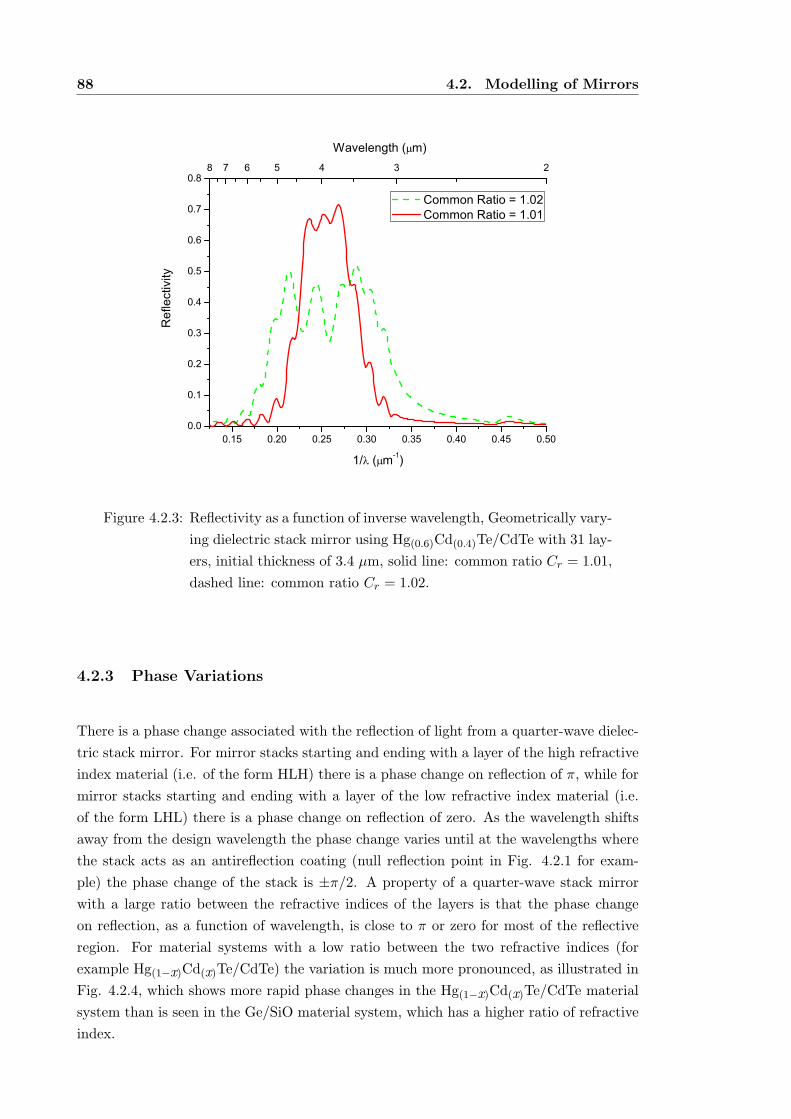
88 4.2. Modelling of Mirrors
0.15 0.20 0.25 0.30 0.35 0.40 0.45 0.500.0
0.1
0.2
0.3
0.4
0.5
0.6
0.7
0.88 7 6 5 4 3 2
Reflectivity
1/ ( m-1)
Common Ratio = 1.02 Common Ratio = 1.01
Wavelength ( m)
Figure 4.2.3: Reflectivity as a function of inverse wavelength, Geometrically vary-
ing dielectric stack mirror using Hg(0.6)Cd(0.4)Te/CdTe with 31 lay-
ers, initial thickness of 3.4 µm, solid line: common ratio Cr = 1.01,
dashed line: common ratio Cr = 1.02.
4.2.3 Phase Variations
There is a phase change associated with the reflection of light from a quarter-wave dielec-
tric stack mirror. For mirror stacks starting and ending with a layer of the high refractive
index material (i.e. of the form HLH) there is a phase change on reflection of π, while for
mirror stacks starting and ending with a layer of the low refractive index material (i.e.
of the form LHL) there is a phase change on reflection of zero. As the wavelength shifts
away from the design wavelength the phase change varies until at the wavelengths where
the stack acts as an antireflection coating (null reflection point in Fig. 4.2.1 for exam-
ple) the phase change of the stack is ±π/2. A property of a quarter-wave stack mirror
with a large ratio between the refractive indices of the layers is that the phase change
on reflection, as a function of wavelength, is close to π or zero for most of the reflective
region. For material systems with a low ratio between the two refractive indices (for
example Hg(1−x)Cd(x)Te/CdTe) the variation is much more pronounced, as illustrated in
Fig. 4.2.4, which shows more rapid phase changes in the Hg(1−x)Cd(x)Te/CdTe material
system than is seen in the Ge/SiO material system, which has a higher ratio of refractive
index.
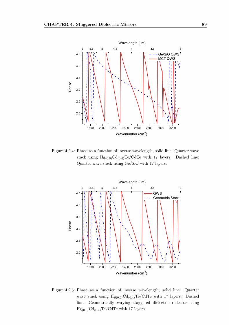
CHAPTER 4. Staggered Dielectric Mirrors 89
1800 2000 2200 2400 2600 2800 3000 3200
2.0
2.5
3.0
3.5
4.0
4.5
6 5.5 5 4.5 4 3.5 3
Phase
Wavenumber (cm-1)
Ge/SiO QWS MCT QWS
Wavelength ( m)
Figure 4.2.4: Phase as a function of inverse wavelength, solid line: Quarter wave
stack using Hg(0.6)Cd(0.4)Te/CdTe with 17 layers. Dashed line:
Quarter wave stack using Ge/SiO with 17 layers.
1800 2000 2200 2400 2600 2800 3000 3200
2.0
2.5
3.0
3.5
4.0
4.5
6 5.5 5 4.5 4 3.5 3
Phase
Wavenumber (cm-1)
QWS Geometric Stack
Wavelength ( m)
Figure 4.2.5: Phase as a function of inverse wavelength, solid line: Quarter
wave stack using Hg(0.6)Cd(0.4)Te/CdTe with 17 layers. Dashed
line: Geometrically varying staggered dielectric reflector using
Hg(0.6)Cd(0.4)Te/CdTe with 17 layers.
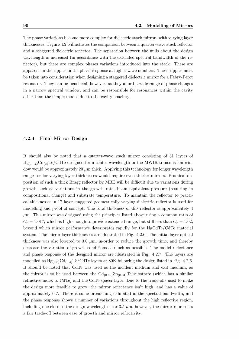
90 4.2. Modelling of Mirrors
The phase variations become more complex for dielectric stack mirrors with varying layer
thicknesses. Figure 4.2.5 illustrates the comparison between a quarter-wave stack reflector
and a staggered dielectric reflector. The separation between the nulls about the design
wavelength is increased (in accordance with the extended spectral bandwidth of the re-
flector), but there are complex phases variations introduced into the stack. These are
apparent in the ripples in the phase response at higher wave numbers. These ripples must
be taken into consideration when designing a staggered dielectric mirror for a Fabry-Perot
resonator. They can be beneficial, however, as they afford a wide range of phase changes
in a narrow spectral window, and can be responsible for resonances within the cavity
other than the simple modes due to the cavity spacing.
4.2.4 Final Mirror Design
It should also be noted that a quarter-wave stack mirror consisting of 31 layers of
Hg(1−x)Cd(x)Te/CdTe designed for a center wavelength in the MWIR transmission win-
dow would be approximately 20 µm thick. Applying this technology for longer wavelength
ranges or for varying layer thicknesses would require even thicker mirrors. Practical de-
position of such a thick Bragg reflector by MBE will be difficult due to variations during
growth such as variations in the growth rate, beam equivalent pressure (resulting in
compositional change) and substrate temperature. To maintain the reflector to practi-
cal thicknesses, a 17 layer staggered geometrically varying dielectric reflector is used for
modelling and proof of concept. The total thickness of this reflector is approximately 4
µm. This mirror was designed using the principles listed above using a common ratio of
Cr = 1.017, which is high enough to provide extended range, but still less than Cr = 1.02,
beyond which mirror performance deteriorates rapidly for the HgCdTe/CdTe material
system. The mirror layer thicknesses are illustrated in Fig. 4.2.6. The initial layer optical
thickness was also lowered to 3.0 µm, in-order to reduce the growth time, and thereby
decrease the variation of growth conditions as much as possible. The model reflectance
and phase response of the designed mirror are illustrated in Fig. 4.2.7. The layers are
modelled as Hg(0.6)Cd(0.4)Te/CdTe layers at 80K following the design listed in Fig. 4.2.6.
It should be noted that CdTe was used as the incident medium and exit medium, as
the mirror is to be used between the Cd(0.96)Zn(0.04)Te substrate (which has a similar
refractive index to CdTe) and the CdTe spacer layer. Due to the trade-offs used to make
the design more feasible to grow, the mirror reflectance isn’t high, and has a value of
approximately 0.7. There is some broadening exhibited in the spectral bandwidth, and
the phase response shows a number of variations throughout the high reflective region,
including one close to the design wavelength near 3.5 µm, however, the mirror represents
a fair trade-off between ease of growth and mirror reflectivity.
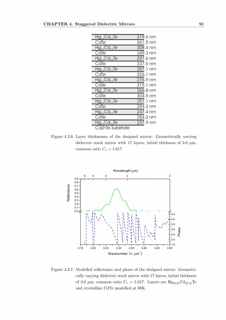
CHAPTER 4. Staggered Dielectric Mirrors 91
237.9 nm284.2 nm247.4 nm294.2 nm257.1 nm304.5 nm266.8 nm315.1 nm276.9 nm326.1 nm287.1 nm337.5 nm297.6 nm349.3 nm308.4 nm361.5 nm319.6 nm
Hg Cd Te0.6 0.4
CdTeHg Cd Te0.6 0.4
Hg Cd Te0.6 0.4
Hg Cd Te0.6 0.4
Hg Cd Te0.6 0.4
Hg Cd Te0.6 0.4
Hg Cd Te0.6 0.4
Hg Cd Te0.6 0.4
Hg Cd Te0.6 0.4
CdTe
CdTe
CdTe
CdTe
CdTe
CdTe
CdTe
CdZnTe Substrate
Figure 4.2.6: Layer thicknesses of the designed mirror: Geometrically varying
dielectric stack mirror with 17 layers, initial thickness of 3.0 µm,
common ratio Cr = 1.017
0.15 0.20 0.25 0.30 0.35 0.40 0.45 0.50
0.00.10.20.30.40.50.60.70.80.9
1.5
2.0
2.5
3.0
3.5
4.0
4.5
6 5 4 3 2
Ref
lect
ance
Wavenumber 1/ ( m-1)
Pha
se
Wavelength ( m)
Figure 4.2.7: Modelled reflectance and phase of the designed mirror: Geometri-
cally varying dielectric stack mirror with 17 layers, initial thickness
of 3.0 µm, common ratio Cr = 1.017. Layers are Hg(0.6)Cd(0.4)Te
and crystalline CdTe modelled at 80K.
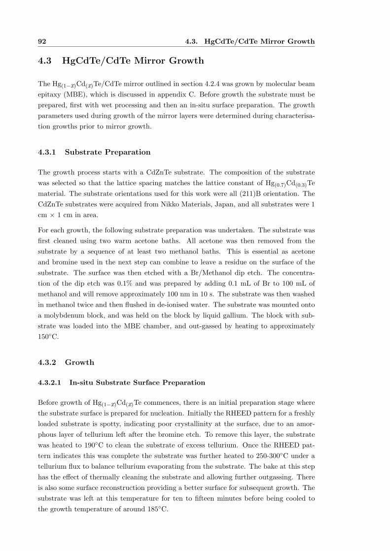
92 4.3. HgCdTe/CdTe Mirror Growth
4.3 HgCdTe/CdTe Mirror Growth
The Hg(1−x)Cd(x)Te/CdTe mirror outlined in section 4.2.4 was grown by molecular beam
epitaxy (MBE), which is discussed in appendix C. Before growth the substrate must be
prepared, first with wet processing and then an in-situ surface preparation. The growth
parameters used during growth of the mirror layers were determined during characterisa-
tion growths prior to mirror growth.
4.3.1 Substrate Preparation
The growth process starts with a CdZnTe substrate. The composition of the substrate
was selected so that the lattice spacing matches the lattice constant of Hg(0.7)Cd(0.3)Te
material. The substrate orientations used for this work were all (211)B orientation. The
CdZnTe substrates were acquired from Nikko Materials, Japan, and all substrates were 1
cm × 1 cm in area.
For each growth, the following substrate preparation was undertaken. The substrate was
first cleaned using two warm acetone baths. All acetone was then removed from the
substrate by a sequence of at least two methanol baths. This is essential as acetone
and bromine used in the next step can combine to leave a residue on the surface of the
substrate. The surface was then etched with a Br/Methanol dip etch. The concentra-
tion of the dip etch was 0.1% and was prepared by adding 0.1 mL of Br to 100 mL of
methanol and will remove approximately 100 nm in 10 s. The substrate was then washed
in methanol twice and then flushed in de-ionised water. The substrate was mounted onto
a molybdenum block, and was held on the block by liquid gallium. The block with sub-
strate was loaded into the MBE chamber, and out-gassed by heating to approximately
150C.
4.3.2 Growth
4.3.2.1 In-situ Substrate Surface Preparation
Before growth of Hg(1−x)Cd(x)Te commences, there is an initial preparation stage where
the substrate surface is prepared for nucleation. Initially the RHEED pattern for a freshly
loaded substrate is spotty, indicating poor crystallinity at the surface, due to an amor-
phous layer of tellurium left after the bromine etch. To remove this layer, the substrate
was heated to 190C to clean the substrate of excess tellurium. Once the RHEED pat-
tern indicates this was complete the substrate was further heated to 250-300C under a
tellurium flux to balance tellurium evaporating from the substrate. The bake at this step
has the effect of thermally cleaning the substrate and allowing further outgassing. There
is also some surface reconstruction providing a better surface for subsequent growth. The
substrate was left at this temperature for ten to fifteen minutes before being cooled to
the growth temperature of around 185C.
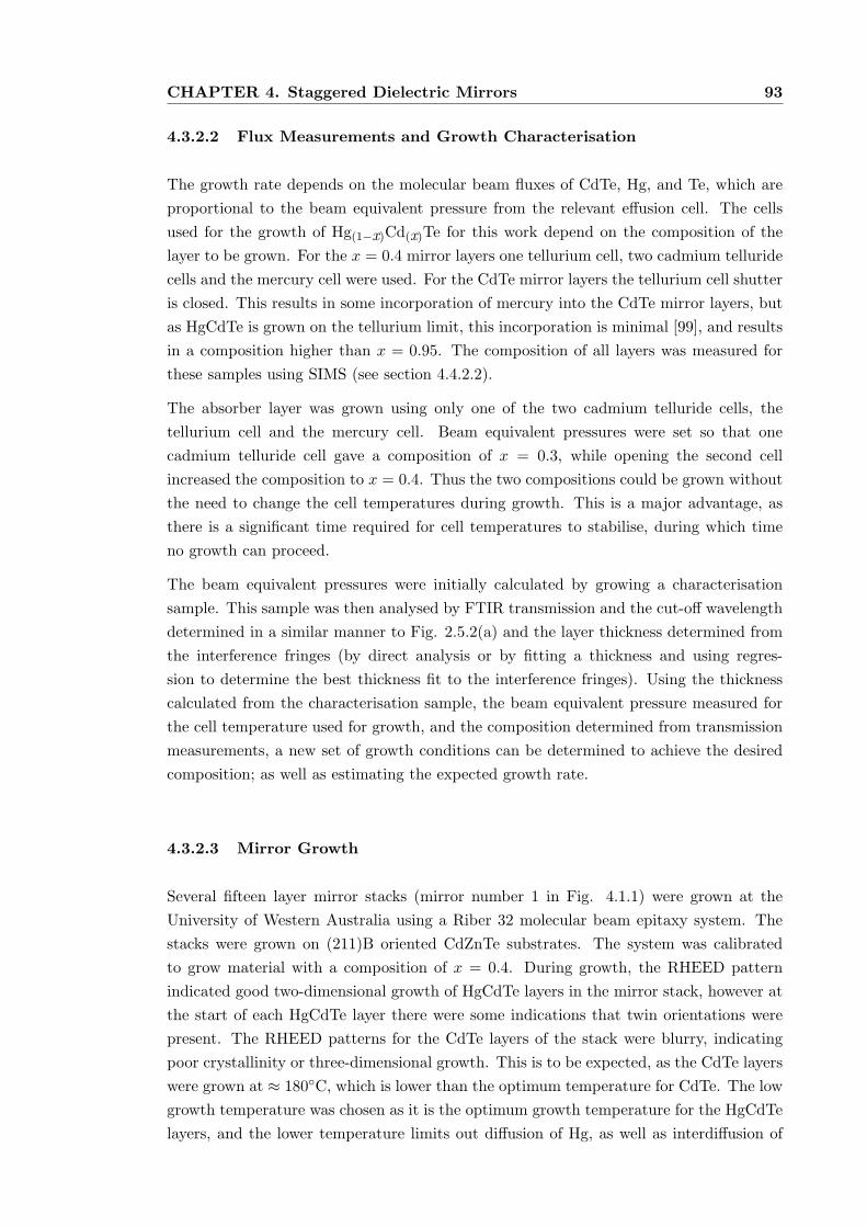
CHAPTER 4. Staggered Dielectric Mirrors 93
4.3.2.2 Flux Measurements and Growth Characterisation
The growth rate depends on the molecular beam fluxes of CdTe, Hg, and Te, which are
proportional to the beam equivalent pressure from the relevant effusion cell. The cells
used for the growth of Hg(1−x)Cd(x)Te for this work depend on the composition of the
layer to be grown. For the x = 0.4 mirror layers one tellurium cell, two cadmium telluride
cells and the mercury cell were used. For the CdTe mirror layers the tellurium cell shutter
is closed. This results in some incorporation of mercury into the CdTe mirror layers, but
as HgCdTe is grown on the tellurium limit, this incorporation is minimal [99], and results
in a composition higher than x = 0.95. The composition of all layers was measured for
these samples using SIMS (see section 4.4.2.2).
The absorber layer was grown using only one of the two cadmium telluride cells, the
tellurium cell and the mercury cell. Beam equivalent pressures were set so that one
cadmium telluride cell gave a composition of x = 0.3, while opening the second cell
increased the composition to x = 0.4. Thus the two compositions could be grown without
the need to change the cell temperatures during growth. This is a major advantage, as
there is a significant time required for cell temperatures to stabilise, during which time
no growth can proceed.
The beam equivalent pressures were initially calculated by growing a characterisation
sample. This sample was then analysed by FTIR transmission and the cut-off wavelength
determined in a similar manner to Fig. 2.5.2(a) and the layer thickness determined from
the interference fringes (by direct analysis or by fitting a thickness and using regres-
sion to determine the best thickness fit to the interference fringes). Using the thickness
calculated from the characterisation sample, the beam equivalent pressure measured for
the cell temperature used for growth, and the composition determined from transmission
measurements, a new set of growth conditions can be determined to achieve the desired
composition; as well as estimating the expected growth rate.
4.3.2.3 Mirror Growth
Several fifteen layer mirror stacks (mirror number 1 in Fig. 4.1.1) were grown at the
University of Western Australia using a Riber 32 molecular beam epitaxy system. The
stacks were grown on (211)B oriented CdZnTe substrates. The system was calibrated
to grow material with a composition of x = 0.4. During growth, the RHEED pattern
indicated good two-dimensional growth of HgCdTe layers in the mirror stack, however at
the start of each HgCdTe layer there were some indications that twin orientations were
present. The RHEED patterns for the CdTe layers of the stack were blurry, indicating
poor crystallinity or three-dimensional growth. This is to be expected, as the CdTe layers
were grown at ≈ 180C, which is lower than the optimum temperature for CdTe. The low
growth temperature was chosen as it is the optimum growth temperature for the HgCdTe
layers, and the lower temperature limits out diffusion of Hg, as well as interdiffusion of
94 4.3. HgCdTe/CdTe Mirror Growth
Figure 4.3.1: SEM micrograph of as grown mirror structure taken using a Zeiss
1555 SUPRA Variable Pressure FESEM using an accelerating volt-
age of 1 kV. The brighter layers are the HgCdTe, while the darker
layers are CdTe.
Hg and Cd in the mirror layers. The HgCdTe layers still returned to crystalline growth
on these CdTe layers after the initial twinned regions discussed above.
Figure 4.3.1 is an SEM micrograph of a cross section of the as-grown layers, showing
sharp interfaces with the lighter stripes being the HgCdTe. The dark region at the top of
the image is the photo-resist that was used to protect the sample when it was cleaved for
the SEM micrograph. The thicknesses of the individual layers were measured from the
SEM micrograph. The general geometric trend in thickness was maintained, although the
common ratio between the layer thicknesses was less than expected, most likely due to
variations in the beam fluxes during growth, which resulted in a decreasing growth rate as
the growth progressed, and effectively making the stack appear closer to a quarter-wave
stack.
CHAPTER 4. Staggered Dielectric Mirrors 95
HgCdTeSample
QuartzTube
QuartzCaplet
QuartzRod
Hg Reservoir
Figure 4.3.2: Schematic of the apparatus used for annealing of HgCdTe samples
in a Hg atmosphere.
4.3.3 Annealing
Even extrinsically doped as-grown MBE layers of Hg(1−x)Cd(x)Te are generally of mixed
conduction type, typically requiring an anneal to convert the mixed type material to one
uniform type [100]. Furthermore, some types of damage introduced during fabrication
steps can be reduced by annealing [101, 102] so that annealing is a common process step in
Hg(1−x)Cd(x)Te detector fabrication. There are various methods for annealing; typically
the process is used to produce n-type Hg(1−x)Cd(x)Te, activate dopants or reduce damage,
and involves annealing in a Hg atmosphere to fill Hg vacancies and thereby producing
n-type material. In contrast, vacancy-doped p-type material is formed by annealing under
vacuum or low Hg overpressure conditions, resulting in the introduction of vacancies into
the material.
Annealing at UWA is performed in quartz ampoules, formed from two quartz tubes, one
placed inverted inside the other (see Fig 4.3.2). All quartz glass wear is cleaned in a
HF:H2O solution prior to use, and ensures that impurities are minimised. The ampoule is
evacuated by a turbo-molecular pump, which is separated from the ampoule by a liquid
nitrogen trap. Once the pressure inside the ampoule is sufficiently low, the ampoule is
sealed by melting the quartz tubes with an O2-H2 flame. Care is taken during the sealing
process to keep the sample temperature low. The sample is placed within two quartz
caplets (Fig. 4.3.2) to protect the sample and prevent mercury droplets from coming into
contact with the sample. The mercury reservoir is also placed within two quartz caplets,
and separated from the sample by a quartz rod.
The anneal is performed in an oven that is preheated to the desired annealing temperature.
The ampoule is placed into the oven with the sample end of the ampoule located at the
centre of the oven, which is the hottest region. The thermocouple controlling the oven
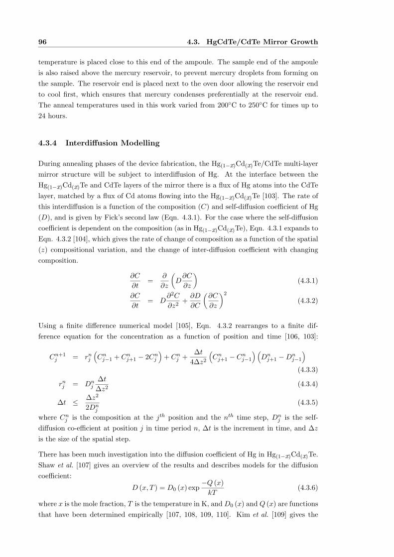
96 4.3. HgCdTe/CdTe Mirror Growth
temperature is placed close to this end of the ampoule. The sample end of the ampoule
is also raised above the mercury reservoir, to prevent mercury droplets from forming on
the sample. The reservoir end is placed next to the oven door allowing the reservoir end
to cool first, which ensures that mercury condenses preferentially at the reservoir end.
The anneal temperatures used in this work varied from 200C to 250C for times up to
24 hours.
4.3.4 Interdiffusion Modelling
During annealing phases of the device fabrication, the Hg(1−x)Cd(x)Te/CdTe multi-layer
mirror structure will be subject to interdiffusion of Hg. At the interface between the
Hg(1−x)Cd(x)Te and CdTe layers of the mirror there is a flux of Hg atoms into the CdTe
layer, matched by a flux of Cd atoms flowing into the Hg(1−x)Cd(x)Te [103]. The rate of
this interdiffusion is a function of the composition (C) and self-diffusion coefficient of Hg
(D), and is given by Fick’s second law (Eqn. 4.3.1). For the case where the self-diffusion
coefficient is dependent on the composition (as in Hg(1−x)Cd(x)Te), Eqn. 4.3.1 expands to
Eqn. 4.3.2 [104], which gives the rate of change of composition as a function of the spatial
(z) compositional variation, and the change of inter-diffusion coefficient with changing
composition.
∂C
∂t=
∂
∂z
(
D∂C
∂z
)
(4.3.1)
∂C
∂t= D
∂2C
∂z2+∂D
∂C
(
∂C
∂z
)2
(4.3.2)
Using a finite difference numerical model [105], Eqn. 4.3.2 rearranges to a finite dif-
ference equation for the concentration as a function of position and time [106, 103]:
Cn+1j = rn
j
(
Cnj−1 + Cn
j+1 − 2Cnj
)
+ Cnj +
∆t
4∆z2
(
Cnj+1 − Cn
j−1
) (
Dnj+1 −Dn
j−1
)
(4.3.3)
rnj = Dn
j
∆t
∆z2(4.3.4)
∆t ≤ ∆z2
2Dnj
(4.3.5)
where Cnj is the composition at the jth position and the nth time step, Dn
j is the self-
diffusion co-efficient at position j in time period n, ∆t is the increment in time, and ∆z
is the size of the spatial step.
There has been much investigation into the diffusion coefficient of Hg in Hg(1−x)Cd(x)Te.
Shaw et al. [107] gives an overview of the results and describes models for the diffusion
coefficient:
D (x, T ) = D0 (x) exp−Q (x)
kT(4.3.6)
where x is the mole fraction, T is the temperature in K, andD0 (x) and Q (x) are functions
that have been determined empirically [107, 108, 109, 110]. Kim et al. [109] gives the
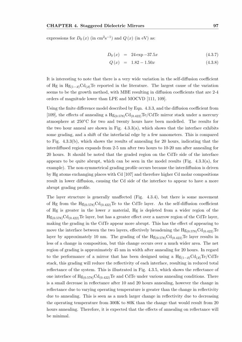
CHAPTER 4. Staggered Dielectric Mirrors 97
expressions for D0 (x) (in cm2s−1) and Q (x) (in eV) as:
D0 (x) = 24 exp−37.5x (4.3.7)
Q (x) = 1.82 − 1.50x (4.3.8)
It is interesting to note that there is a very wide variation in the self-diffusion coefficient
of Hg in Hg(1−x)Cd(x)Te reported in the literature. The largest cause of the variation
seems to be the growth method, with MBE resulting in diffusion coefficients that are 2-4
orders of magnitude lower than LPE and MOCVD [111, 109].
Using the finite difference model described by Eqn. 4.3.3, and the diffusion coefficient from
[109], the effects of annealing a Hg(0.578)Cd(0.422)Te/CdTe mirror stack under a mercury
atmosphere at 250C for two and twenty hours have been modelled. The results for
the two hour anneal are shown in Fig. 4.3.3(a), which shows that the interface exhibits
some grading, and a shift of the interfacial edge by a few nanometers. This is compared
to Fig. 4.3.3(b), which shows the results of annealing for 20 hours, indicating that the
interdiffused region expands from 2-5 nm after two hours to 10-20 nm after annealing for
20 hours. It should be noted that the graded region on the CdTe side of the interface
appears to be quite abrupt, which can be seen in the model results (Fig. 4.3.3(a), for
example). The non-symmetrical grading profile occurs because the interdiffusion is driven
by Hg atoms exchanging places with Cd [107] and therefore higher Cd molar compositions
result in lower diffusion, causing the Cd side of the interface to appear to have a more
abrupt grading profile.
The layer structure is generally unaffected (Fig. 4.3.4), but there is some movement
of Hg from the Hg(0.578)Cd(0.422)Te to the CdTe layer. As the self-diffusion coefficient
of Hg is greater in the lower x material, Hg is depleted from a wider region of the
Hg(0.578)Cd(0.422)Te layer, but has a greater effect over a narrow region of the CdTe layer,
making the grading in the CdTe appear more abrupt. This has the effect of appearing to
move the interface between the two layers, effectively broadening the Hg(0.578)Cd(0.422)Te
layer by approximately 10 nm. The grading of the Hg(0.578)Cd(0.422)Te layer results in
less of a change in composition, but this change occurs over a much wider area. The net
region of grading is approximately 45 nm in width after annealing for 20 hours. In regard
to the performance of a mirror that has been designed using a Hg(1−x)Cd(x)Te/CdTe
stack, this grading will reduce the reflectivity of each interface, resulting in reduced total
reflectance of the system. This is illustrated in Fig. 4.3.5, which shows the reflectance of
one interface of Hg(0.578)Cd(0.422)Te and CdTe under various annealing conditions. There
is a small decrease in reflectance after 10 and 20 hours annealing, however the change in
reflectance due to varying operating temperature is greater than the change in reflectivity
due to annealing. This is seen as a much larger change in reflectivity due to decreasing
the operating temperature from 300K to 80K than the change that would result from 20
hours annealing. Therefore, it is expected that the effects of annealing on reflectance will
be minimal.
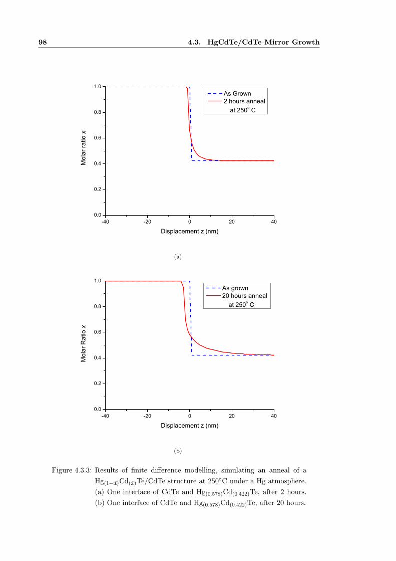
98 4.3. HgCdTe/CdTe Mirror Growth
-40 -20 0 20 400.0
0.2
0.4
0.6
0.8
1.0M
olar
ratio
x
Displacement z (nm)
As Grown 2 hours anneal
at 250o C
(a)
-40 -20 0 20 400.0
0.2
0.4
0.6
0.8
1.0
Mol
ar R
atio
x
Displacement z (nm)
As grown 20 hours anneal
at 250o C
(b)
Figure 4.3.3: Results of finite difference modelling, simulating an anneal of a
Hg(1−x)Cd(x)Te/CdTe structure at 250C under a Hg atmosphere.
(a) One interface of CdTe and Hg(0.578)Cd(0.422)Te, after 2 hours.
(b) One interface of CdTe and Hg(0.578)Cd(0.422)Te, after 20 hours.
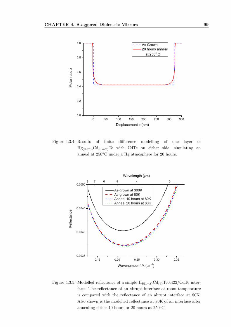
CHAPTER 4. Staggered Dielectric Mirrors 99
0 50 100 150 200 250 300 3500.0
0.2
0.4
0.6
0.8
1.0
Mol
ar ra
tio x
Displacement z (nm)
As Grown 20 hours anneal
at 250o C
Figure 4.3.4: Results of finite difference modelling of one layer of
Hg(0.578)Cd(0.422)Te with CdTe on either side, simulating an
anneal at 250C under a Hg atmosphere for 20 hours.
0.15 0.20 0.25 0.30 0.350.0035
0.0040
0.0045
0.00508 7 6 5 4 3
Reflectan
ce
Wavenumber 1/ ( m-1)
As-grown at 300K As-grown at 80K Anneal 10 hours at 80K Anneal 20 hours at 80K
Wavelength ( m)
Figure 4.3.5: Modelled reflectance of a simple Hg(1−x)Cd(x)Te0.422/CdTe inter-
face. The reflectance of an abrupt interface at room temperature
is compared with the reflectance of an abrupt interface at 80K.
Also shown is the modelled reflectance at 80K of an interface after
annealing either 10 hours or 20 hours at 250C.
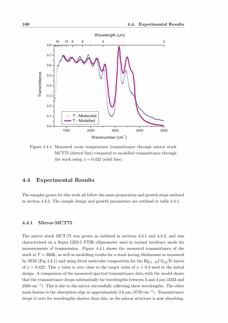
100 4.4. Experimental Results
Figure 4.4.1: Measured room temperature transmittance through mirror stack
MCT75 (dotted line) compared to modelled transmittance through
the stack using x = 0.422 (solid line).
4.4 Experimental Results
The samples grown for this work all follow the same preparation and growth steps outlined
in section 4.3.2. The sample design and growth parameters are outlined in table 4.4.1.
4.4.1 Mirror-MCT75
The mirror stack MCT-75 was grown as outlined in sections 4.3.1 and 4.3.2, and was
characterised on a Sopra GES-5 FTIR ellipsometer used in normal incidence mode for
measurements of transmission. Figure 4.4.1 shows the measured transmittance of the
stack at T = 300K, as well as modelling results for a stack having thicknesses as measured
by SEM (Fig 4.3.1) and using fitted molecular composition for the Hg(1−x)Cd(x)Te layers
of x = 0.422. This x value is very close to the target value of x = 0.4 used in the initial
design. A comparison of the measured spectral transmittance data with the model shows
that the transmittance drops substantially for wavelengths between 3 and 4 µm (3333 and
2500 cm−1). This is due to the mirror successfully reflecting these wavelengths. The other
main feature is the absorption edge at approximately 2.6 µm (3750 cm−1). Transmittance
drops to zero for wavelengths shorter than this, as the mirror structure is now absorbing.
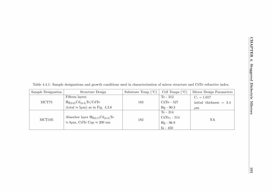
CH
AP
TER
4.
Sta
ggere
dD
iele
ctric
Mirro
rs101
Table 4.4.1: Sample designations and growth conditions used in characterisation of mirror structure and CdTe refractive index.
Sample Designation Structure Design Substrate Temp (C) Cell Temps (C) Mirror Design Parameters
MCT75
Fifteen layers
Hg(0.6)Cd(0.4)Te/CdTe
(total ≈ 5µm) as in Fig. 4.2.6
183
Te - 312
CdTe - 527
Hg - 90.3
Cr = 1.017
initial thickness = 3.4
µm
MCT105Absorber layer Hg(0.7)Cd(0.3)Te
≈ 8µm, CdTe Cap ≈ 200 nm182
Te - 314
CdTe1 - 514
Hg - 96.9
In - 450
NA
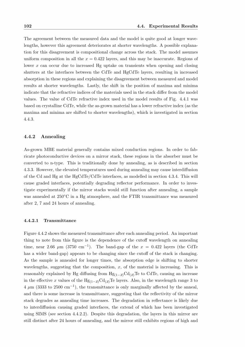
102 4.4. Experimental Results
The agreement between the measured data and the model is quite good at longer wave-
lengths, however this agreement deteriorates at shorter wavelengths. A possible explana-
tion for this disagreement is compositional change across the stack. The model assumes
uniform composition in all the x = 0.422 layers, and this may be inaccurate. Regions of
lower x can occur due to increased Hg uptake on transients when opening and closing
shutters at the interfaces between the CdTe and HgCdTe layers, resulting in increased
absorption in these regions and explaining the disagreement between measured and model
results at shorter wavelengths. Lastly, the shift in the position of maxima and minima
indicate that the refractive indices of the materials used in the stack differ from the model
values. The value of CdTe refractive index used in the model results of Fig. 4.4.1 was
based on crystalline CdTe, while the as-grown material has a lower refractive index (as the
maxima and minima are shifted to shorter wavelengths), which is investigated in section
4.4.3.
4.4.2 Annealing
As-grown MBE material generally contains mixed conduction regions. In order to fab-
ricate photoconductive devices on a mirror stack, these regions in the absorber must be
converted to n-type. This is traditionally done by annealing, as is described in section
4.3.3. However, the elevated temperatures used during annealing may cause interdiffusion
of the Cd and Hg at the HgCdTe/CdTe interfaces, as modelled in section 4.3.4. This will
cause graded interfaces, potentially degrading reflector performance. In order to inves-
tigate experimentally if the mirror stacks would still function after annealing, a sample
was annealed at 250C in a Hg atmosphere, and the FTIR transmittance was measured
after 2, 7 and 24 hours of annealing.
4.4.2.1 Transmittance
Figure 4.4.2 shows the measured transmittance after each annealing period. An important
thing to note from this figure is the dependence of the cutoff wavelength on annealing
time, near 2.66 µm (3750 cm−1). The band-gap of the x = 0.422 layers (the CdTe
has a wider band-gap) appears to be changing since the cutoff of the stack is changing.
As the sample is annealed for longer times, the absorption edge is shifting to shorter
wavelengths, suggesting that the composition, x, of the material is increasing. This is
reasonably explained by Hg diffusing from Hg(1−x)Cd(x)Te to CdTe, causing an increase
in the effective x values of the Hg(1−x)Cd(x)Te layers. Also, in the wavelength range 3 to
4 µm (3333 to 2500 cm−1), the transmittance is only marginally affected by the anneal,
and there is some increase in transmittance, suggesting that the reflectivity of the mirror
stack degrades as annealing time increases. The degradation in reflectance is likely due
to interdiffusion causing graded interfaces, the extend of which has been investigated
using SIMS (see section 4.4.2.2). Despite this degradation, the layers in this mirror are
still distinct after 24 hours of annealing, and the mirror still exhibits regions of high and
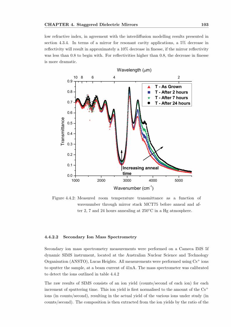
CHAPTER 4. Staggered Dielectric Mirrors 103
low refractive index, in agreement with the interdiffusion modelling results presented in
section 4.3.4. In terms of a mirror for resonant cavity applications, a 5% decrease in
reflectivity will result in approximately a 10% decrease in finesse, if the mirror reflectivity
was less than 0.8 to begin with. For reflectivities higher than 0.8, the decrease in finesse
is more dramatic.
Figure 4.4.2: Measured room temperature transmittance as a function of
wavenumber through mirror stack MCT75 before anneal and af-
ter 2, 7 and 24 hours annealing at 250C in a Hg atmosphere.
4.4.2.2 Secondary Ion Mass Spectrometry
Secondary ion mass spectrometry measurements were performed on a Cameca IMS 5f
dynamic SIMS instrument, located at the Australian Nuclear Science and Technology
Organisation (ANSTO), Lucas Heights. All measurements were performed using Cs+ ions
to sputter the sample, at a beam current of 41nA. The mass spectrometer was calibrated
to detect the ions outlined in table 4.4.2
The raw results of SIMS consists of an ion yield (counts/second of each ion) for each
increment of sputtering time. This ion yield is first normalised to the amount of the Cs+
ions (in counts/second), resulting in the actual yield of the various ions under study (in
counts/second). The composition is then extracted from the ion yields by the ratio of the
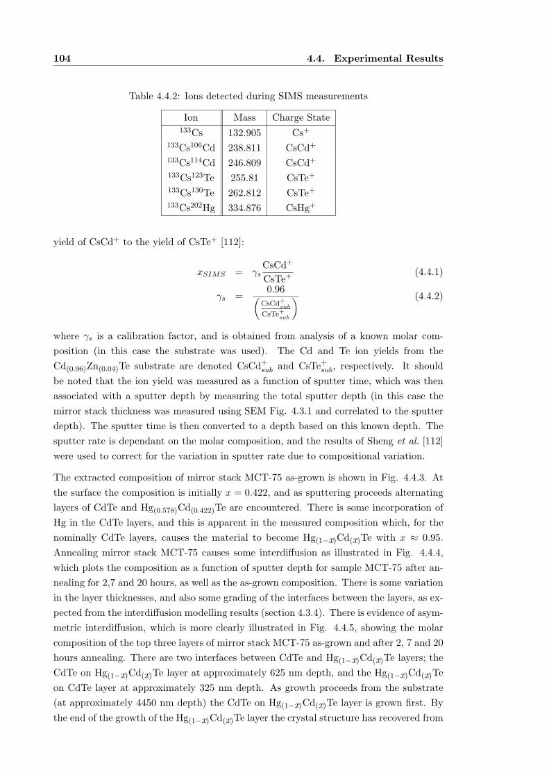
104 4.4. Experimental Results
Table 4.4.2: Ions detected during SIMS measurements
Ion Mass Charge State133Cs 132.905 Cs+
133Cs106Cd 238.811 CsCd+
133Cs114Cd 246.809 CsCd+
133Cs123Te 255.81 CsTe+
133Cs130Te 262.812 CsTe+
133Cs202Hg 334.876 CsHg+
yield of CsCd+ to the yield of CsTe+ [112]:
xSIMS = γsCsCd+
CsTe+ (4.4.1)
γs =0.96
(
CsCd+
sub
CsTe+sub
) (4.4.2)
where γs is a calibration factor, and is obtained from analysis of a known molar com-
position (in this case the substrate was used). The Cd and Te ion yields from the
Cd(0.96)Zn(0.04)Te substrate are denoted CsCd+sub and CsTe+
sub, respectively. It should
be noted that the ion yield was measured as a function of sputter time, which was then
associated with a sputter depth by measuring the total sputter depth (in this case the
mirror stack thickness was measured using SEM Fig. 4.3.1 and correlated to the sputter
depth). The sputter time is then converted to a depth based on this known depth. The
sputter rate is dependant on the molar composition, and the results of Sheng et al. [112]
were used to correct for the variation in sputter rate due to compositional variation.
The extracted composition of mirror stack MCT-75 as-grown is shown in Fig. 4.4.3. At
the surface the composition is initially x = 0.422, and as sputtering proceeds alternating
layers of CdTe and Hg(0.578)Cd(0.422)Te are encountered. There is some incorporation of
Hg in the CdTe layers, and this is apparent in the measured composition which, for the
nominally CdTe layers, causes the material to become Hg(1−x)Cd(x)Te with x ≈ 0.95.
Annealing mirror stack MCT-75 causes some interdiffusion as illustrated in Fig. 4.4.4,
which plots the composition as a function of sputter depth for sample MCT-75 after an-
nealing for 2,7 and 20 hours, as well as the as-grown composition. There is some variation
in the layer thicknesses, and also some grading of the interfaces between the layers, as ex-
pected from the interdiffusion modelling results (section 4.3.4). There is evidence of asym-
metric interdiffusion, which is more clearly illustrated in Fig. 4.4.5, showing the molar
composition of the top three layers of mirror stack MCT-75 as-grown and after 2, 7 and 20
hours annealing. There are two interfaces between CdTe and Hg(1−x)Cd(x)Te layers; the
CdTe on Hg(1−x)Cd(x)Te layer at approximately 625 nm depth, and the Hg(1−x)Cd(x)Te
on CdTe layer at approximately 325 nm depth. As growth proceeds from the substrate
(at approximately 4450 nm depth) the CdTe on Hg(1−x)Cd(x)Te layer is grown first. By
the end of the growth of the Hg(1−x)Cd(x)Te layer the crystal structure has recovered from
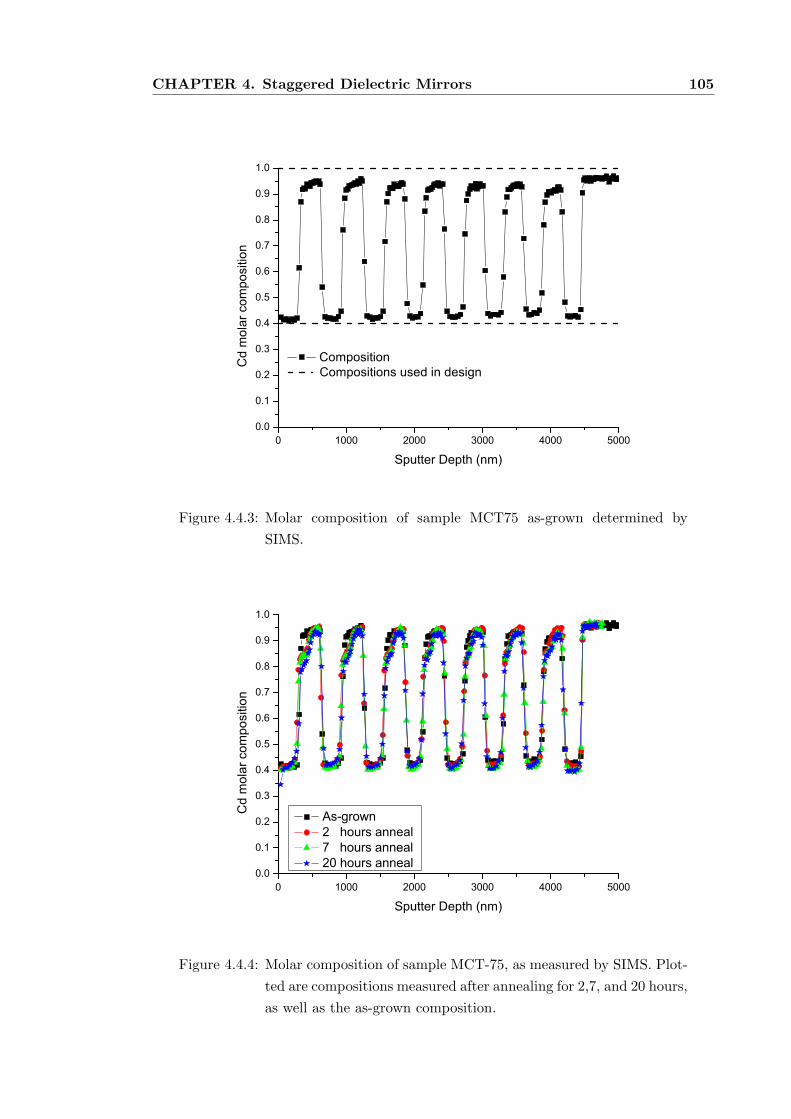
CHAPTER 4. Staggered Dielectric Mirrors 105
0 1000 2000 3000 4000 50000.0
0.1
0.2
0.3
0.4
0.5
0.6
0.7
0.8
0.9
1.0
CompositionCd
mol
ar c
ompo
sitio
n
Sputter Depth (nm)
Compositions used in design
Figure 4.4.3: Molar composition of sample MCT75 as-grown determined by
SIMS.
0 1000 2000 3000 4000 50000.0
0.1
0.2
0.3
0.4
0.5
0.6
0.7
0.8
0.9
1.0
Cd
mol
ar c
ompo
sitio
n
Sputter Depth (nm)
As-grown 2 hours anneal 7 hours anneal 20 hours anneal
Figure 4.4.4: Molar composition of sample MCT-75, as measured by SIMS. Plot-
ted are compositions measured after annealing for 2,7, and 20 hours,
as well as the as-grown composition.
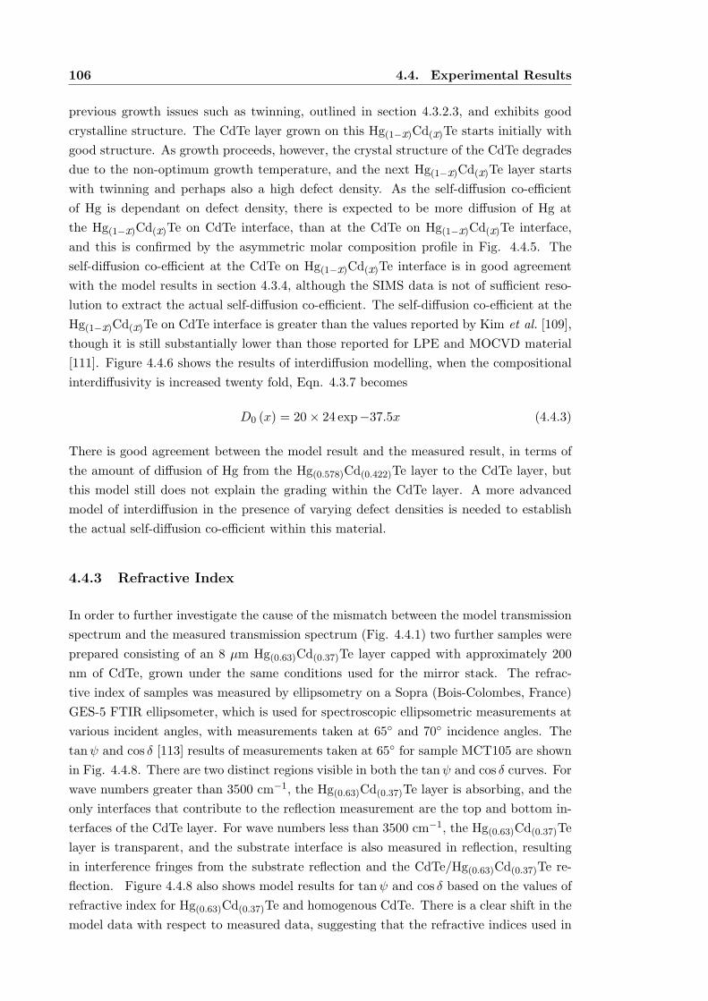
106 4.4. Experimental Results
previous growth issues such as twinning, outlined in section 4.3.2.3, and exhibits good
crystalline structure. The CdTe layer grown on this Hg(1−x)Cd(x)Te starts initially with
good structure. As growth proceeds, however, the crystal structure of the CdTe degrades
due to the non-optimum growth temperature, and the next Hg(1−x)Cd(x)Te layer starts
with twinning and perhaps also a high defect density. As the self-diffusion co-efficient
of Hg is dependant on defect density, there is expected to be more diffusion of Hg at
the Hg(1−x)Cd(x)Te on CdTe interface, than at the CdTe on Hg(1−x)Cd(x)Te interface,
and this is confirmed by the asymmetric molar composition profile in Fig. 4.4.5. The
self-diffusion co-efficient at the CdTe on Hg(1−x)Cd(x)Te interface is in good agreement
with the model results in section 4.3.4, although the SIMS data is not of sufficient reso-
lution to extract the actual self-diffusion co-efficient. The self-diffusion co-efficient at the
Hg(1−x)Cd(x)Te on CdTe interface is greater than the values reported by Kim et al. [109],
though it is still substantially lower than those reported for LPE and MOCVD material
[111]. Figure 4.4.6 shows the results of interdiffusion modelling, when the compositional
interdiffusivity is increased twenty fold, Eqn. 4.3.7 becomes
D0 (x) = 20 × 24 exp−37.5x (4.4.3)
There is good agreement between the model result and the measured result, in terms of
the amount of diffusion of Hg from the Hg(0.578)Cd(0.422)Te layer to the CdTe layer, but
this model still does not explain the grading within the CdTe layer. A more advanced
model of interdiffusion in the presence of varying defect densities is needed to establish
the actual self-diffusion co-efficient within this material.
4.4.3 Refractive Index
In order to further investigate the cause of the mismatch between the model transmission
spectrum and the measured transmission spectrum (Fig. 4.4.1) two further samples were
prepared consisting of an 8 µm Hg(0.63)Cd(0.37)Te layer capped with approximately 200
nm of CdTe, grown under the same conditions used for the mirror stack. The refrac-
tive index of samples was measured by ellipsometry on a Sopra (Bois-Colombes, France)
GES-5 FTIR ellipsometer, which is used for spectroscopic ellipsometric measurements at
various incident angles, with measurements taken at 65 and 70 incidence angles. The
tanψ and cos δ [113] results of measurements taken at 65 for sample MCT105 are shown
in Fig. 4.4.8. There are two distinct regions visible in both the tanψ and cos δ curves. For
wave numbers greater than 3500 cm−1, the Hg(0.63)Cd(0.37)Te layer is absorbing, and the
only interfaces that contribute to the reflection measurement are the top and bottom in-
terfaces of the CdTe layer. For wave numbers less than 3500 cm−1, the Hg(0.63)Cd(0.37)Te
layer is transparent, and the substrate interface is also measured in reflection, resulting
in interference fringes from the substrate reflection and the CdTe/Hg(0.63)Cd(0.37)Te re-
flection. Figure 4.4.8 also shows model results for tanψ and cos δ based on the values of
refractive index for Hg(0.63)Cd(0.37)Te and homogenous CdTe. There is a clear shift in the
model data with respect to measured data, suggesting that the refractive indices used in
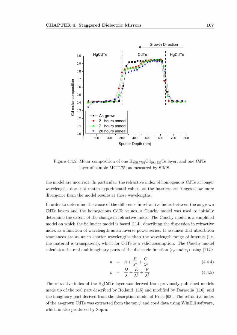
CHAPTER 4. Staggered Dielectric Mirrors 107
0 100 200 300 400 500 600 700 8000.0
0.1
0.2
0.3
0.4
0.5
0.6
0.7
0.8
0.9
1.0 HgCdTeCdTe
Cd
mol
ar c
ompo
sitio
n
Sputter Depth (nm)
As-grown 2 hours anneal 7 hours anneal 20 hours anneal
HgCdTe
Growth Direction
Figure 4.4.5: Molar composition of one Hg(0.578)Cd(0.422)Te layer, and one CdTe
layer of sample MCT-75, as measured by SIMS.
the model are incorrect. In particular, the refractive index of homogenous CdTe at longer
wavelengths does not match experimental values, as the interference fringes show more
divergence from the model results at these wavelengths.
In order to determine the cause of the difference in refractive index between the as-grown
CdTe layers and the homogenous CdTe values, a Cauchy model was used to initially
determine the extent of the change in refractive index. The Cauchy model is a simplified
model on which the Sellmeier model is based [114], describing the dispersion in refractive
index as a function of wavelength as an inverse power series. It assumes that absorbtion
resonances are at much shorter wavelengths than the wavelength range of interest (i.e.
the material is transparent), which for CdTe is a valid assumption. The Cauchy model
calculates the real and imaginary parts of the dielectric function (εr and εi) using [114]:
n = A+B
λ2+C
λ4(4.4.4)
k =D
λ+E
λ3+F
λ5(4.4.5)
The refractive index of the HgCdTe layer was derived from previously published models
made up of the real part described by Rolland [115] and modified by Daraselia [116], and
the imaginary part derived from the absorption model of Price [63]. The refractive index
of the as-grown CdTe was extracted from the tanψ and cos δ data using WinElli software,
which is also produced by Sopra.
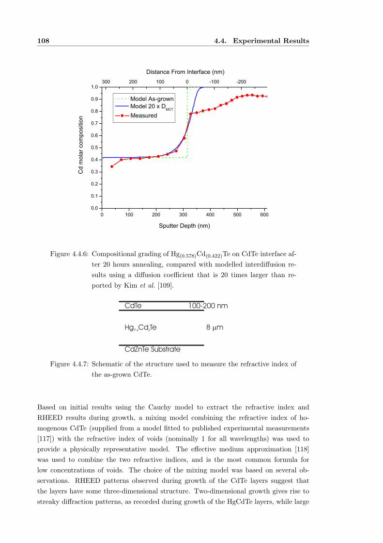
108 4.4. Experimental Results
0.0
0.1
0.2
0.3
0.4
0.5
0.6
0.7
0.8
0.9
1.0
0 100 200 300 400 500 600
300 200 100 0 -100 -200C
d m
olar
com
posi
tion
Sputter Depth (nm)
Model As-grown Model 20 x D
MCT
Measured
Distance From Interface (nm)
Figure 4.4.6: Compositional grading of Hg(0.578)Cd(0.422)Te on CdTe interface af-
ter 20 hours annealing, compared with modelled interdiffusion re-
sults using a diffusion coefficient that is 20 times larger than re-
ported by Kim et al. [109].
8 mm
100-200 nm
Hg Cd Te1-x x
CdTe
CdZnTe Substrate
Figure 4.4.7: Schematic of the structure used to measure the refractive index of
the as-grown CdTe.
Based on initial results using the Cauchy model to extract the refractive index and
RHEED results during growth, a mixing model combining the refractive index of ho-
mogenous CdTe (supplied from a model fitted to published experimental measurements
[117]) with the refractive index of voids (nominally 1 for all wavelengths) was used to
provide a physically representative model. The effective medium approximation [118]
was used to combine the two refractive indices, and is the most common formula for
low concentrations of voids. The choice of the mixing model was based on several ob-
servations. RHEED patterns observed during growth of the CdTe layers suggest that
the layers have some three-dimensional structure. Two-dimensional growth gives rise to
streaky diffraction patterns, as recorded during growth of the HgCdTe layers, while large
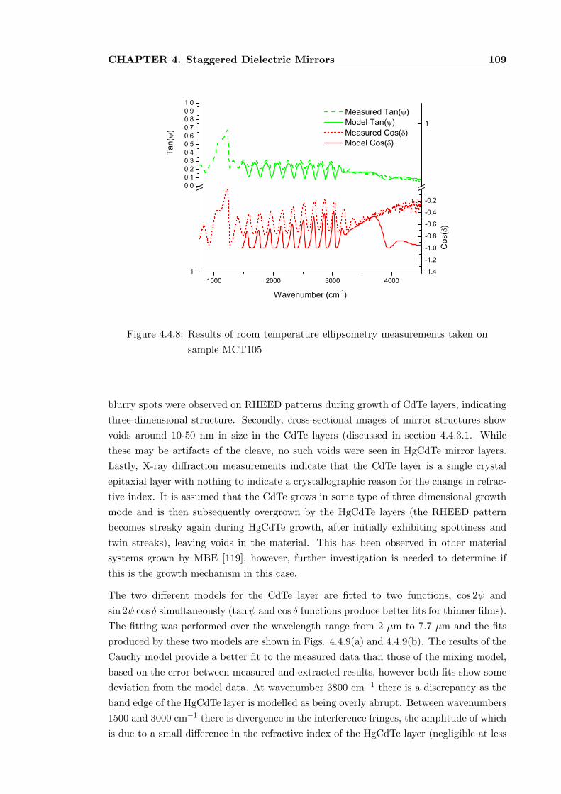
CHAPTER 4. Staggered Dielectric Mirrors 109
1000 2000 3000 4000-1
0.00.10.20.30.40.50.60.70.80.91.0
-1.4
-1.2
-1.0
-0.8
-0.6
-0.4
-0.2
1
Tan(
)
Wavenumber (cm-1)
Measured Tan( ) Model Tan( )
Cos
()
Measured Cos( ) Model Cos( )
Figure 4.4.8: Results of room temperature ellipsometry measurements taken on
sample MCT105
blurry spots were observed on RHEED patterns during growth of CdTe layers, indicating
three-dimensional structure. Secondly, cross-sectional images of mirror structures show
voids around 10-50 nm in size in the CdTe layers (discussed in section 4.4.3.1. While
these may be artifacts of the cleave, no such voids were seen in HgCdTe mirror layers.
Lastly, X-ray diffraction measurements indicate that the CdTe layer is a single crystal
epitaxial layer with nothing to indicate a crystallographic reason for the change in refrac-
tive index. It is assumed that the CdTe grows in some type of three dimensional growth
mode and is then subsequently overgrown by the HgCdTe layers (the RHEED pattern
becomes streaky again during HgCdTe growth, after initially exhibiting spottiness and
twin streaks), leaving voids in the material. This has been observed in other material
systems grown by MBE [119], however, further investigation is needed to determine if
this is the growth mechanism in this case.
The two different models for the CdTe layer are fitted to two functions, cos 2ψ and
sin 2ψ cos δ simultaneously (tanψ and cos δ functions produce better fits for thinner films).
The fitting was performed over the wavelength range from 2 µm to 7.7 µm and the fits
produced by these two models are shown in Figs. 4.4.9(a) and 4.4.9(b). The results of the
Cauchy model provide a better fit to the measured data than those of the mixing model,
based on the error between measured and extracted results, however both fits show some
deviation from the model data. At wavenumber 3800 cm−1 there is a discrepancy as the
band edge of the HgCdTe layer is modelled as being overly abrupt. Between wavenumbers
1500 and 3000 cm−1 there is divergence in the interference fringes, the amplitude of which
is due to a small difference in the refractive index of the HgCdTe layer (negligible at less
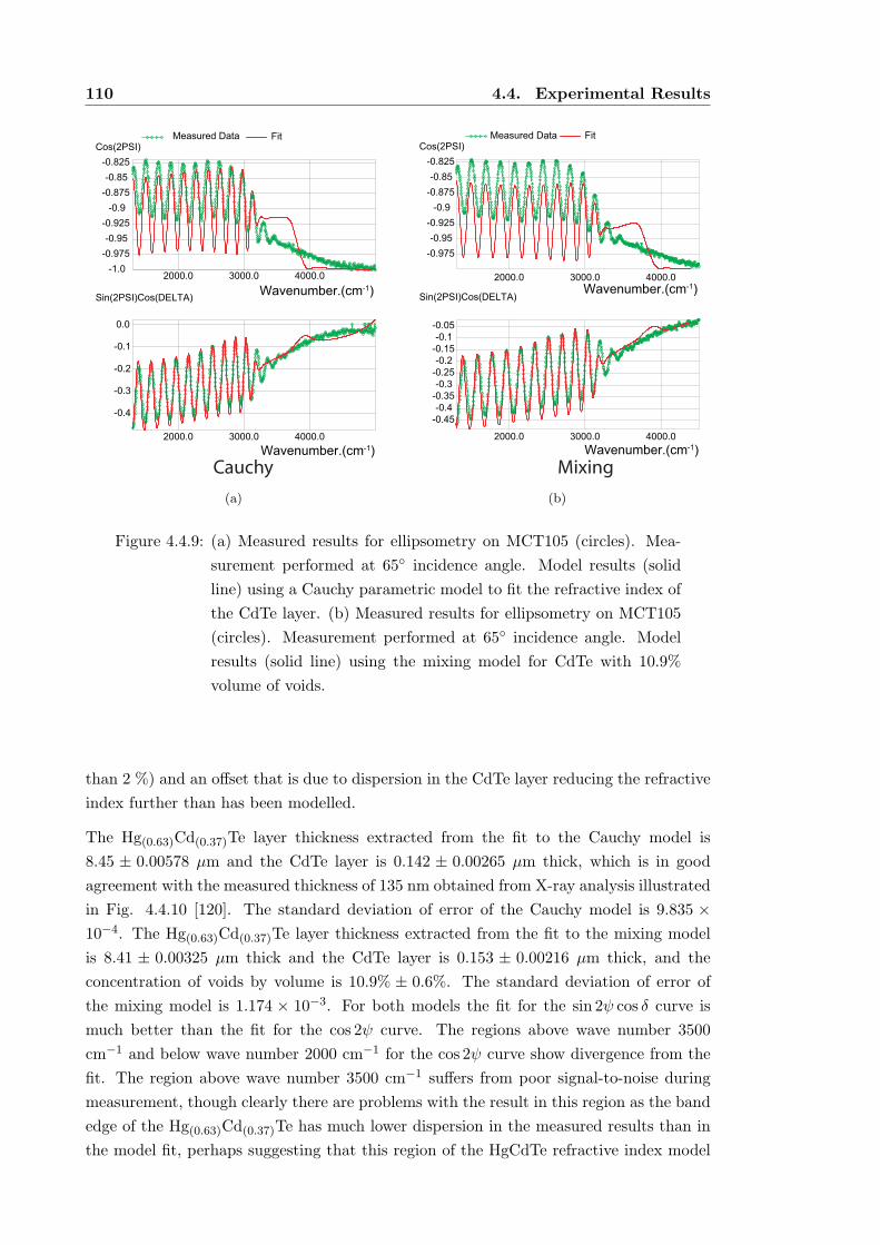
110 4.4. Experimental Results
2000.0 3000.0 4000.0-1.0
-0.975
-0.95
-0.925
-0.9
-0.875
-0.85
-0.825
2000.0 3000.0 4000.0
-0.4
-0.3
-0.2
-0.1
0.0
Sin(2PSI)Cos(DELTA)
Measured Data Fit
Wavenumber.(cm-1)
Cos(2PSI)
Wavenumber.(cm-1)
Cauchy
(a)
2000.0 3000.0 4000.0
-0.975
-0.95
-0.925
-0.9
-0.875
-0.85
-0.825
2000.0 3000.0 4000.0
-0.45
-0.4
-0.35
-0.3
-0.25
-0.2
-0.15
-0.1
-0.05
Sin(2PSI)Cos(DELTA)
Measured Data Fit
Wavenumber.(cm-1)
Cos(2PSI)
Wavenumber.(cm-1)
Mixing
(b)
Figure 4.4.9: (a) Measured results for ellipsometry on MCT105 (circles). Mea-
surement performed at 65 incidence angle. Model results (solid
line) using a Cauchy parametric model to fit the refractive index of
the CdTe layer. (b) Measured results for ellipsometry on MCT105
(circles). Measurement performed at 65 incidence angle. Model
results (solid line) using the mixing model for CdTe with 10.9%
volume of voids.
than 2 %) and an offset that is due to dispersion in the CdTe layer reducing the refractive
index further than has been modelled.
The Hg(0.63)Cd(0.37)Te layer thickness extracted from the fit to the Cauchy model is
8.45 ± 0.00578 µm and the CdTe layer is 0.142 ± 0.00265 µm thick, which is in good
agreement with the measured thickness of 135 nm obtained from X-ray analysis illustrated
in Fig. 4.4.10 [120]. The standard deviation of error of the Cauchy model is 9.835 ×10⁻⁴. The Hg(0.63)Cd(0.37)Te layer thickness extracted from the fit to the mixing model
is 8.41 ± 0.00325 µm thick and the CdTe layer is 0.153 ± 0.00216 µm thick, and the
concentration of voids by volume is 10.9% ± 0.6%. The standard deviation of error of
the mixing model is 1.174 × 10⁻³. For both models the fit for the sin 2ψ cos δ curve is
much better than the fit for the cos 2ψ curve. The regions above wave number 3500
cm−1 and below wave number 2000 cm−1 for the cos 2ψ curve show divergence from the
fit. The region above wave number 3500 cm−1 suffers from poor signal-to-noise during
measurement, though clearly there are problems with the result in this region as the band
edge of the Hg(0.63)Cd(0.37)Te has much lower dispersion in the measured results than in
the model fit, perhaps suggesting that this region of the HgCdTe refractive index model
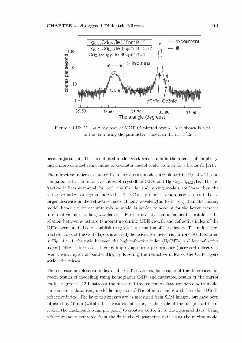
CHAPTER 4. Staggered Dielectric Mirrors 111
35.50
1
10
counts
per
second
100
1000
35.60
135nm R=0
R=0.77
R=1
Theta angle (degrees)35.70 35.80
experiment
35.90
fit
Hg0.08Cd0.92Te
8.5µmHg0.63Cd0.37Te
800µmCd0.96Zn0.04Te
=> Thickness
CdTe
HgCdTe CdZnTe
Figure 4.4.10: 2θ − ω x-ray scan of MCT105 plotted over θ. Also shown is a fit
to the data using the parameters shown in the inset [120].
needs adjustment. The model used in this work was chosen in the interest of simplicity,
and a more detailed semiconductor oscillator model could be used for a better fit [121].
The refractive indices extracted from the various models are plotted in Fig. 4.4.11, and
compared with the refractive index of crystalline CdTe and Hg(0.63)Cd(0.37)Te. The re-
fractive indices extracted for both the Cauchy and mixing models are lower than the
refractive index for crystalline CdTe. The Cauchy model is more accurate as it has a
larger decrease in the refractive index at long wavelengths (6-10 µm) than the mixing
model, hence a more accurate mixing model is needed to account for the larger decrease
in refractive index at long wavelengths. Further investigation is required to establish the
relation between substrate temperature during MBE growth and refractive index of the
CdTe layers, and also to establish the growth mechanism of these layers. The reduced re-
fractive index of the CdTe layers is actually beneficial for dielectric mirrors. As illustrated
in Fig. 4.4.11, the ratio between the high refractive index (HgCdTe) and low refractive
index (CdTe) is increased, thereby improving mirror performance (increased reflectivity
over a wider spectral bandwidth), by lowering the refractive index of the CdTe layers
within the mirror.
The decrease in refractive index of the CdTe layers explains some of the differences be-
tween results of modelling using homogenous CdTe and measured results of the mirror
stack. Figure 4.4.12 illustrates the measured transmittance data compared with model
transmittance data using model homogenous CdTe refractive index and the reduced CdTe
refractive index. The layer thicknesses are as measured from SEM images, but have been
adjusted by 10 nm (within the measurement error, as the scale of the image used to es-
tablish the thickness is 5 nm per pixel) to create a better fit to the measured data. Using
refractive index extracted from the fit to the ellipsometric data using the mixing model
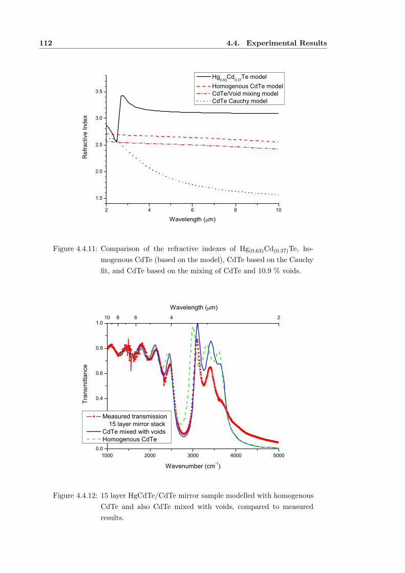
112 4.4. Experimental Results
2 4 6 8 10
1.5
2.0
2.5
3.0
3.5R
efra
ctiv
e In
dex
Wavelength ( m)
Hg0.63
Cd0.37
Te model Homogenous CdTe model CdTe/Void mixing model CdTe Cauchy model
Figure 4.4.11: Comparison of the refractive indexes of Hg(0.63)Cd(0.37)Te, ho-
mogenous CdTe (based on the model), CdTe based on the Cauchy
fit, and CdTe based on the mixing of CdTe and 10.9 % voids.
1000 2000 3000 4000 50000.0
0.2
0.4
0.6
0.8
1.010 8 6 4 2
Tran
smittan
ce
Wavenumber (cm-1)
Measured transmission 15 layer mirror stack
CdTe mixed with voids Homogenous CdTe
Wavelength ( m)
Figure 4.4.12: 15 layer HgCdTe/CdTe mirror sample modelled with homogenous
CdTe and also CdTe mixed with voids, compared to measured
results.
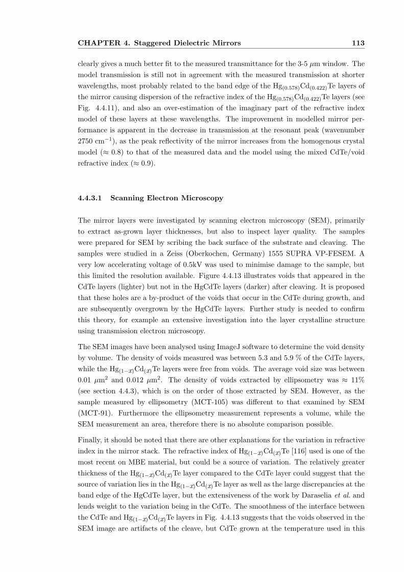
CHAPTER 4. Staggered Dielectric Mirrors 113
clearly gives a much better fit to the measured transmittance for the 3-5 µm window. The
model transmission is still not in agreement with the measured transmission at shorter
wavelengths, most probably related to the band edge of the Hg(0.578)Cd(0.422)Te layers of
the mirror causing dispersion of the refractive index of the Hg(0.578)Cd(0.422)Te layers (see
Fig. 4.4.11), and also an over-estimation of the imaginary part of the refractive index
model of these layers at these wavelengths. The improvement in modelled mirror per-
formance is apparent in the decrease in transmission at the resonant peak (wavenumber
2750 cm−1), as the peak reflectivity of the mirror increases from the homogenous crystal
model (≈ 0.8) to that of the measured data and the model using the mixed CdTe/void
refractive index (≈ 0.9).
4.4.3.1 Scanning Electron Microscopy
The mirror layers were investigated by scanning electron microscopy (SEM), primarily
to extract as-grown layer thicknesses, but also to inspect layer quality. The samples
were prepared for SEM by scribing the back surface of the substrate and cleaving. The
samples were studied in a Zeiss (Oberkochen, Germany) 1555 SUPRA VP-FESEM. A
very low accelerating voltage of 0.5kV was used to minimise damage to the sample, but
this limited the resolution available. Figure 4.4.13 illustrates voids that appeared in the
CdTe layers (lighter) but not in the HgCdTe layers (darker) after cleaving. It is proposed
that these holes are a by-product of the voids that occur in the CdTe during growth, and
are subsequently overgrown by the HgCdTe layers. Further study is needed to confirm
this theory, for example an extensive investigation into the layer crystalline structure
using transmission electron microscopy.
The SEM images have been analysed using ImageJ software to determine the void density
by volume. The density of voids measured was between 5.3 and 5.9 % of the CdTe layers,
while the Hg(1−x)Cd(x)Te layers were free from voids. The average void size was between
0.01 µm2 and 0.012 µm2. The density of voids extracted by ellipsometry was ≈ 11%
(see section 4.4.3), which is on the order of those extracted by SEM. However, as the
sample measured by ellipsometry (MCT-105) was different to that examined by SEM
(MCT-91). Furthermore the ellipsometry measurement represents a volume, while the
SEM measurement an area, therefore there is no absolute comparison possible.
Finally, it should be noted that there are other explanations for the variation in refractive
index in the mirror stack. The refractive index of Hg(1−x)Cd(x)Te [116] used is one of the
most recent on MBE material, but could be a source of variation. The relatively greater
thickness of the Hg(1−x)Cd(x)Te layer compared to the CdTe layer could suggest that the
source of variation lies in the Hg(1−x)Cd(x)Te layer as well as the large discrepancies at the
band edge of the HgCdTe layer, but the extensiveness of the work by Daraselia et al. and
lends weight to the variation being in the CdTe. The smoothness of the interface between
the CdTe and Hg(1−x)Cd(x)Te layers in Fig. 4.4.13 suggests that the voids observed in the
SEM image are artifacts of the cleave, but CdTe grown at the temperature used in this
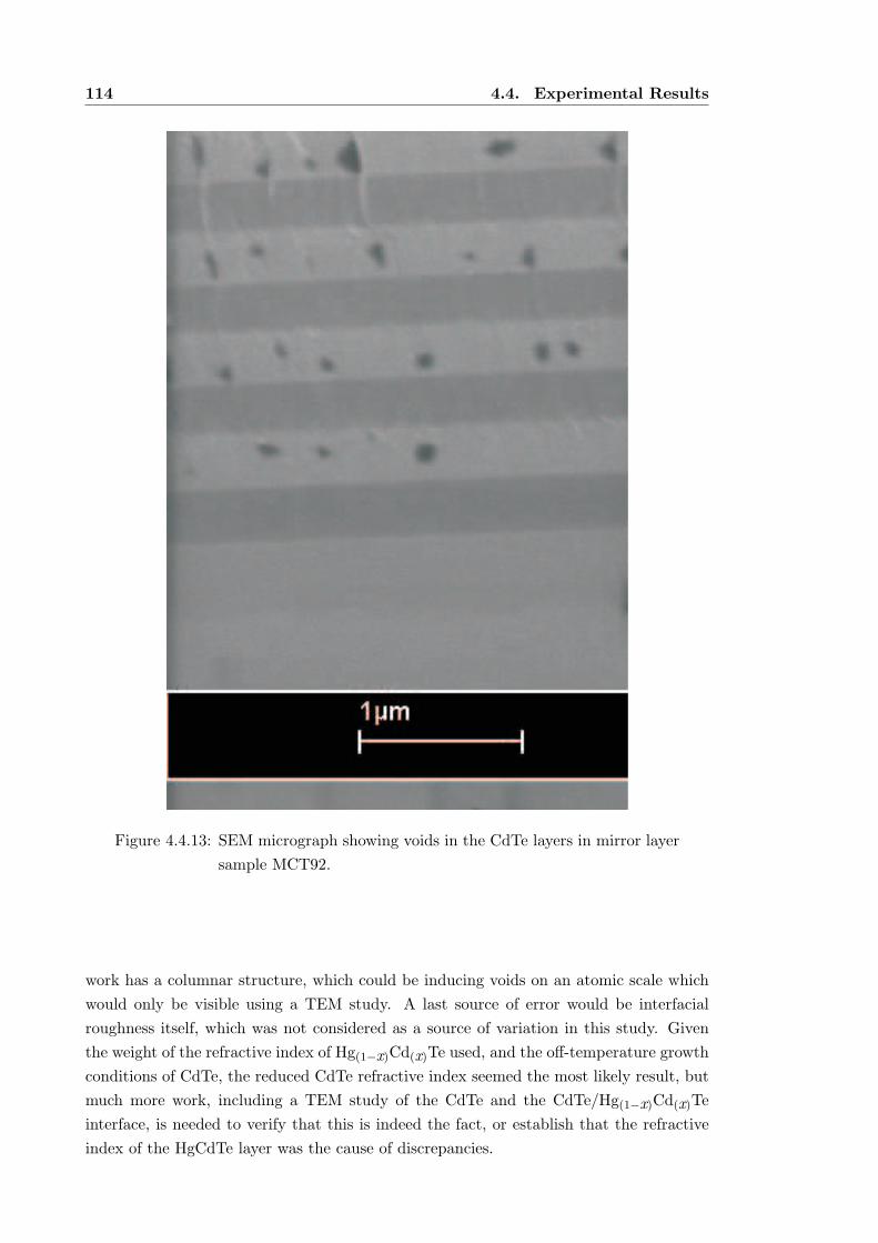
114 4.4. Experimental Results
Figure 4.4.13: SEM micrograph showing voids in the CdTe layers in mirror layer
sample MCT92.
work has a columnar structure, which could be inducing voids on an atomic scale which
would only be visible using a TEM study. A last source of error would be interfacial
roughness itself, which was not considered as a source of variation in this study. Given
the weight of the refractive index of Hg(1−x)Cd(x)Te used, and the off-temperature growth
conditions of CdTe, the reduced CdTe refractive index seemed the most likely result, but
much more work, including a TEM study of the CdTe and the CdTe/Hg(1−x)Cd(x)Te
interface, is needed to verify that this is indeed the fact, or establish that the refractive
index of the HgCdTe layer was the cause of discrepancies.
CHAPTER 4. Staggered Dielectric Mirrors 115
4.5 Conclusions
This chapter has dealt with a number of concepts related to dielectric stack mirrors.
In particular, a dielectric stack mirror fabricated in the Hg(1−x)Cd(x)Te/CdTe material
system was investigated. Mirror design issues were taken into consideration and a mirror
design which broadened the reflectance region of the mirror was established. The mirror
response can be broadened by varying the thicknesses of the mirror layers according to a
geometric or an arithmetic progression. This increases the mirror spectral width at the
expense of the peak reflectivity, and also introduces complex phase variations.
Modelling of interdiffusion of mercury has been performed, and while typical annealing
conditions will cause grading of the interface between mirror layers, the reflectance of the
layer will not be dramatically lowered.
Growth of a Hg(1−x)Cd(x)Te/CdTe mirror by molecular beam epitaxy was also investi-
gated. Mirror performance shows reasonable agreement with model data. Annealing the
dielectric mirror stacks for 24 hours at 250C in a mercury atmosphere does not substan-
tially degrade performance. Investigation of the grading of the interface layers by SIMS
shows that the amount of grading is similar to the grading determined by interdiffusion
modelling. The interdiffusion of mercury shows a dependence on the lattice structure,
with a high self-diffusion co-efficient corresponding to regions of higher defect density.
A more detailed interdiffusion model is needed to further investigate the effects of this
asymmetric interdiffusion. The refractive index of the CdTe layers was also investigated.
The CdTe grown for the mirror stacks was found to have a reduced refractive index, and
resulted in improved mirror performance. The reduced refractive index of the CdTe is
caused by the incorporation of ≈ 10% voids in the material during growth. Voids have
also been observed in SEM images. When mirror performance is re-evaluated using the
new refractive index, very good agreement between model transmittance and measured
transmittance is observed.

116 4.5. Conclusions
Chapter 5Realisation of Resonant-cavity-enhanced
Detectors
5.1 Introduction
The operation of resonant-cavity-enhanced (RCE) detectors have been described in chap-
ter 3, with the technology for fabricating staggered dielectric mirrors investigated and
described in chapter 4. This chapter takes the theory of chapter 3 and investigates the
design, fabrication, and the measured performance of a mid-wave infrared (MWIR) RCE
detector. Measured performance is then compared to modelled performance. The struc-
ture used for the modelling is shown in Fig. 5.1.1, and was investigated with and without
the Ge/SiO mirror 2 using backside and frontside illumination, respectively. This corre-
sponds to the two stages of characterisation undertaken on photoconductors fabricated
using the same structure, which were tested before and after the addition of the Ge/SiO
mirror.
5.2 RCE Detector Design and Modelling
This section discusses the design of the RCE structures. It outlines the general design and
then examines the effects of the phase changes in the staggered dielectric mirror, optimum
cavity length, and optimum positioning of the absorber layer within the structure.
5.2.1 RCE Design
There are a number of trade-offs that must be considered in the design of a RCE detector.
As outlined in section 3.3, the quantum efficiency is linked to the absorption in the cavity,
and the reflectance of the two mirrors. Furthermore, the finesse is determined by the
reflectance of the two mirrors, so device performance is now linked to both the material
118 5.2. RCE Detector Design and Modelling
Cavity L
ength
l
SubstrateCdZnTe
BacksideIllumination
Absorber Hg Cd Te (x=0.3)(1-x) (x) d
Mirror 2
Mirror 1
SiOGe
SiO
Ge
CdTe
CdTeSpacer
Ge
Hg Cd Te(1-x) (x) (x=0.4)
Hg Cd Te(1-x) (x) (x=0.4)
Figure 5.1.1: Schematic RCE device, complete with the ex-situ deposited Ge/SiO
mirror 2.
properties and device dimensions in a significantly more complex relationship than for
a standard detector. Typically, where the finesse is a limiting parameter, the absorber
layer thickness is adjusted to balance the mirror reflectances. Figure 5.2.1 illustrates the
effect of absorber layer thickness on finesse for cavities optimally designed to operate at 4
µm or at 3.4 µm wavelength. As the absorption is higher at 3.4 µm, the finesse is lower.
A finesse of 10 is sufficient for multispectral imagining, therefore 100nm is sufficiently
thin to realise multispectral imaging. However, hyperspectral imaging requires a finesse
of ≈ 100. Therefore, the Hg(1−x)Cd(x)Te absorber layer would need to be very thin, of
the order of 10 nm, or a different material with a lower absorption coefficient is required
in order to achieve a finesse of 100.
As the finesse is not critical for this proof of concept device, an absorber layer thickness of
75nm was chosen, resulting in a detector with a spectral bandwidth in the range required
for multispectral applications. The reflectance of the mirrors was then calculated using
Eqn. 3.3.12, assuming unity reflectance for the back mirror (mirror 2). Using a 75 nm
Hg(0.7)Cd(0.3)Te absorber layer, the required reflectance of the top mirror (mirror 1) for
maximum absorption is 0.835 and 0.777 for wavelengths of 4µm and 3.4µm, respectively.
If a reflectance of 0.777 is used then at 3.4µm wavelength all incident light will be absorbed
in the absorber layer at the resonant wavelength, as light reflected from the cavity under-
goes a π phase change, resulting in a cancellation of all reflected components, or 100% of
energy entering the structure (despite a highly reflective mirror 1). This is illustrated by
the modelled absorptance in Fig. 5.2.2, which shows the modelled absorptance as a func-
tion of wavelength for the structure illustrated in Fig. 5.1.1. Mirror 1 is 6.5 periods (13
layers) of Hg(0.6)Cd(0.4)Te/CdTe in a quarter-wave stack designed for a center wavelength
of 3.4µm, while mirror 2 (which needs to reach unity reflectivity) could either be 21.5
periods of Hg(0.6)Cd(0.4)Te/CdTe or 2.5 periods (5 layers) of Ge/SiO. It is impractical to
CHAPTER 5. Realisation of Resonant-cavity-enhanced Detectors 119
0 20 40 60 80 1000
20
40
60
80
100
120
140
160
180
200
Fine
sse
Absorber Layer Thickness (nm)
4 m wavelength 3.4 m wavelength
Figure 5.2.1: Finesse as a function of absorber thickness, where the absorber is
Hg(0.7)Cd(0.3)Te, for cavities that are designed for optical perfor-
mance at 4 µm and 3.4 µm wavelength.
grow 21.5 periods of MCT/CdTe, and therefore the Ge/SiO material system represents
a much better option for mirror 2, and is technologically feasible. Both material systems
reach unity absorptance at the design wavelength. However, since the MCT/CdTe mirror
(mirror 1) does not have a broad region with high reflectance, there are substantial ab-
sorption lobes at other wavelengths, particularly when using the Ge/SiO material system
for mirror 2. Therefore, the methods investigated in chapter 4 for broadening the spectral
response of the MCT/CdTe mirror need to be applied, resulting in the use of a staggered
mirror design.
5.2.1.1 Staggered Dielectric Mirrors in Resonant-cavity-enhanced Detectors
Staggered dielectric mirrors can be used for RCE detectors, but the design becomes more
convoluted as the complex and rapidly changing phase variations allow resonances to occur
at wavelengths other than integer mode wavelengths. As outlined in section 4.2.3, the
phase variations of staggered dielectric mirrors can result in narrow spectral bandwidth
resonances, which have a weaker dependence on cavity length than on the wavelength of
the phase variation. Furthermore, for a resonant cavity with QWS reflectors optically
designed for the operating wavelength, the resonance generally occurs when the cavity
contains an integer number of halfwaves (i.e. m is an integer for Eqn. 3.3.1). The resonant
condition expressed in Eqn. 3.3.1 must be modified to include the phase contribution of
the staggered dielectric mirror, assuming the QWS has been designed to be centered at
120 5.2. RCE Detector Design and Modelling
2 3 4 5 60.0
0.2
0.4
0.6
0.8
1.0
Abs
orptan
ce
Wavelength ( m)
Hg0.6
Cd0.4
Te/CdTe QWSmirror 2
Ge/SiO mirror 2
Figure 5.2.2: Modelled absorptance of a RCE device with a 75 nm thick
Hg(0.7)Cd(0.3)Te absorber layer. Performance for a device using a
quarter-wave stack of Hg(0.6)Cd(0.4)Te/CdTe for mirror 2 (in Fig.
5.1.1) (dashed line) is compared with that of a device using a
quarter-wave stack using Ge/SiO for mirror 2 (solid line).
the resonant wavelength:
q =φ1 (λ) + φ2 (λ) − 2δ
2π(5.2.1)
where q = 0,±1,±2, ... is the resonant mode and φ1 (λ) and φ2 (λ) are the wavelength
dependent phase changes of the two mirrors, and δ is the phase change associated with
the cavity. Complex phase variations will allow a resonant condition to be established
without the cavity containing an integer number of half waves. Figure 5.2.3 shows the
mode profile at resonance for the structure of Fig. 5.1.1 without mirror 2 but with mirror
2 formed by the CdTe spacer-thin anodic oxide-air interface. The results are shown for
front side illumination, using the thicknesses for mirror 1 outlined in Fig. 4.2.6, at the
resonant wavelength. The modelled structure is similar to the complete RCE devices,
prior the addition of the Ge/SiO mirror layers. There are approximately 1.75 standing
waves in the CdTe spacer that forms the cavity, illustrating the effect of the phase change
in the mirror. This does not make the resonant cavity any less effective at confining the
incident energy, other than the reflectivity trade-off which has been discussed in section
5.2.1, but can decrease the spectral width of the resonance. Adding mirror 2 further
complicates the phase effects within the cavity, and careful design is needed to ensure the
resonant wavelength of the structure occurs at the correct wavelength.
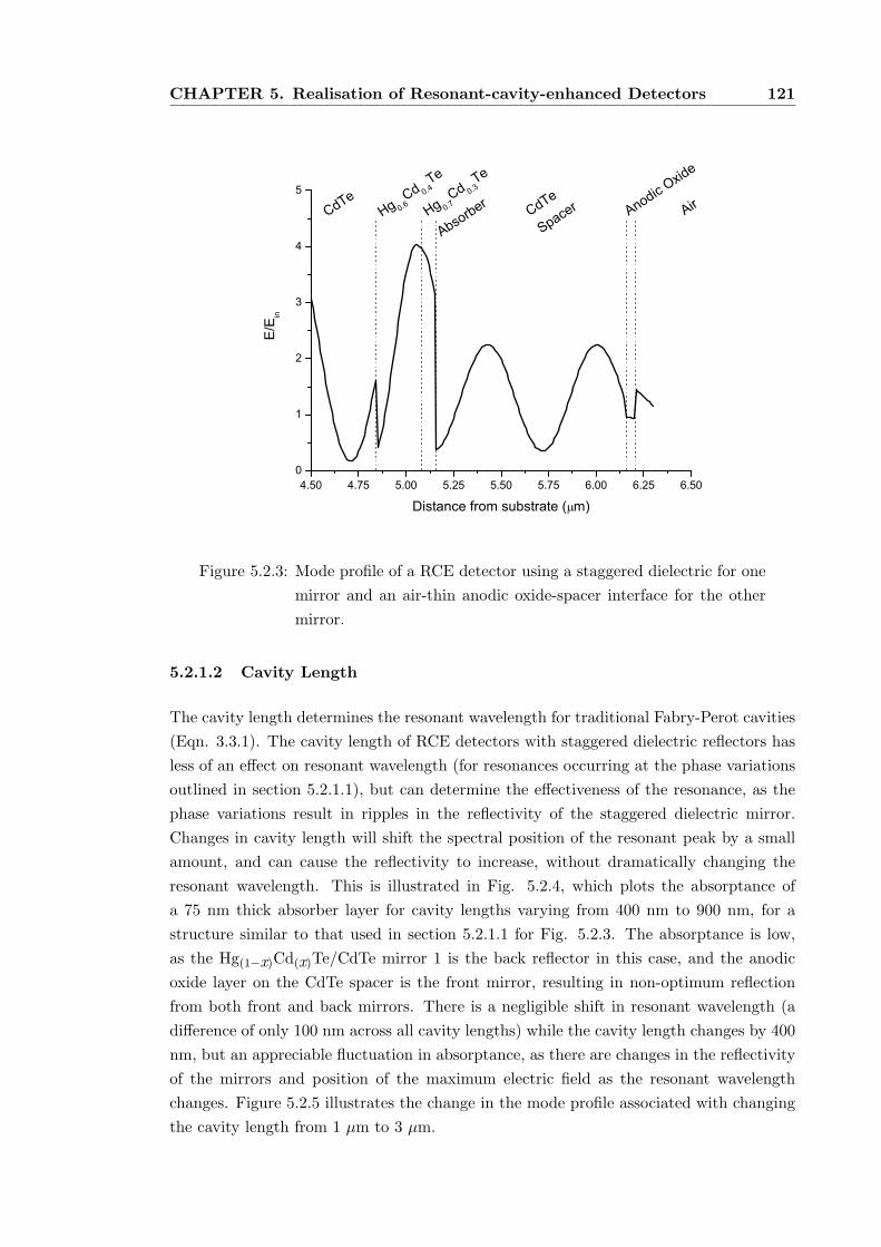
CHAPTER 5. Realisation of Resonant-cavity-enhanced Detectors 121
4.50 4.75 5.00 5.25 5.50 5.75 6.00 6.25 6.500
1
2
3
4
5
AirAnodic Oxid
e
CdTe
SpacerCdTeHg 0.7
Cd 0.3Te
AbsorberHg 0.6Cd 0.4
Te
E/E
in
Distance from substrate ( m)
Figure 5.2.3: Mode profile of a RCE detector using a staggered dielectric for one
mirror and an air-thin anodic oxide-spacer interface for the other
mirror.
5.2.1.2 Cavity Length
The cavity length determines the resonant wavelength for traditional Fabry-Perot cavities
(Eqn. 3.3.1). The cavity length of RCE detectors with staggered dielectric reflectors has
less of an effect on resonant wavelength (for resonances occurring at the phase variations
outlined in section 5.2.1.1), but can determine the effectiveness of the resonance, as the
phase variations result in ripples in the reflectivity of the staggered dielectric mirror.
Changes in cavity length will shift the spectral position of the resonant peak by a small
amount, and can cause the reflectivity to increase, without dramatically changing the
resonant wavelength. This is illustrated in Fig. 5.2.4, which plots the absorptance of
a 75 nm thick absorber layer for cavity lengths varying from 400 nm to 900 nm, for a
structure similar to that used in section 5.2.1.1 for Fig. 5.2.3. The absorptance is low,
as the Hg(1−x)Cd(x)Te/CdTe mirror 1 is the back reflector in this case, and the anodic
oxide layer on the CdTe spacer is the front mirror, resulting in non-optimum reflection
from both front and back mirrors. There is a negligible shift in resonant wavelength (a
difference of only 100 nm across all cavity lengths) while the cavity length changes by 400
nm, but an appreciable fluctuation in absorptance, as there are changes in the reflectivity
of the mirrors and position of the maximum electric field as the resonant wavelength
changes. Figure 5.2.5 illustrates the change in the mode profile associated with changing
the cavity length from 1 µm to 3 µm.
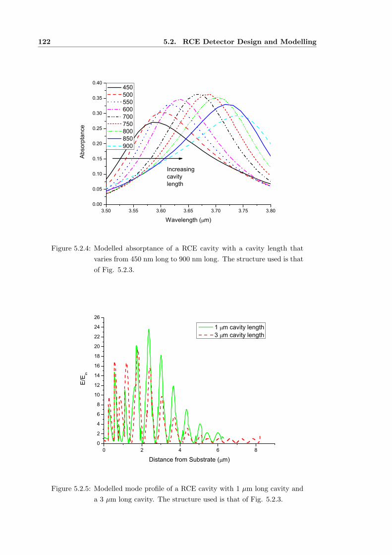
122 5.2. RCE Detector Design and Modelling
3.50 3.55 3.60 3.65 3.70 3.75 3.800.00
0.05
0.10
0.15
0.20
0.25
0.30
0.35
0.40Abs
orptan
ce
Wavelength ( m)
450 500 550 600 700 750 800 850 900
Increasingcavitylength
Figure 5.2.4: Modelled absorptance of a RCE cavity with a cavity length that
varies from 450 nm long to 900 nm long. The structure used is that
of Fig. 5.2.3.
0 2 4 6 80
2
4
6
8
10
12
14
16
18
20
22
24
26
E/E
in
Distance from Substrate ( m)
1 m cavity length 3 m cavity length
Figure 5.2.5: Modelled mode profile of a RCE cavity with 1 µm long cavity and
a 3 µm long cavity. The structure used is that of Fig. 5.2.3.
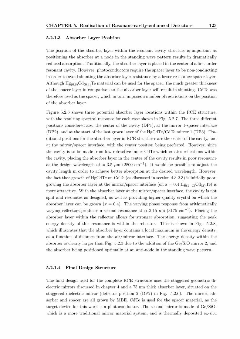
CHAPTER 5. Realisation of Resonant-cavity-enhanced Detectors 123
5.2.1.3 Absorber Layer Position
The position of the absorber layer within the resonant cavity structure is important as
positioning the absorber at a node in the standing wave pattern results in dramatically
reduced absorption. Traditionally, the absorber layer is placed in the center of a first-order
resonant cavity. However, photoconductors require the spacer layer to be non-conducting
in-order to avoid shunting the absorber layer resistance by a lower resistance spacer layer.
Although Hg(0.6)Cd(0.4)Te material can be used for the spacer, the much greater thickness
of the spacer layer in comparison to the absorber layer will result in shunting. CdTe was
therefore used as the spacer, which in turn imposes a number of restrictions on the position
of the absorber layer.
Figure 5.2.6 shows three potential absorber layer locations within the RCE structure,
with the resulting spectral response for each case shown in Fig. 5.2.7. The three different
positions considered are: the center of the cavity (DP1), at the mirror 1-spacer interface
(DP2), and at the start of the last grown layer of the HgCdTe/CdTe mirror 1 (DP3). Tra-
ditional positions for the absorber layer in RCE structures are the center of the cavity, and
at the mirror/spacer interface, with the center position being preferred. However, since
the cavity is to be made from low refractive index CdTe which creates reflections within
the cavity, placing the absorber layer in the center of the cavity results in poor resonance
at the design wavelength of ≈ 3.5 µm (2800 cm−1). It would be possible to adjust the
cavity length in order to achieve better absorption at the desired wavelength. However,
the fact that growth of HgCdTe on CdTe (as discussed in section 4.3.2.3) is initially poor,
growing the absorber layer at the mirror/spacer interface (on x = 0.4 Hg(1−x)Cd(x)Te) is
more attractive. With the absorber layer at the mirror/spacer interface, the cavity is not
split and resonates as designed, as well as providing higher quality crystal on which the
absorber layer can be grown (x = 0.4). The varying phase response from arithmetically
varying reflectors produces a second resonance at ≈ 3.15 µm (3175 cm−1). Placing the
absorber layer within the reflector allows for stronger absorption, suggesting the peak
energy density of this resonance is within the reflector. This is shown in Fig. 5.2.8,
which illustrates that the absorber layer contains a local maximum in the energy density,
as a function of distance from the air/mirror interface. The energy density within the
absorber is clearly larger than Fig. 5.2.3 due to the addition of the Ge/SiO mirror 2, and
the absorber being positioned optimally at an anti-node in the standing wave pattern.
5.2.1.4 Final Design Structure
The final design used for the complete RCE structure uses the staggered geometric di-
electric mirrors discussed in chapter 4 and a 75 nm thick absorber layer, situated on the
staggered dielectric mirror (detector position 2 (DP2) in Fig. 5.2.6). The mirror, ab-
sorber and spacer are all grown by MBE. CdTe is used for the spacer material, as the
target device for this work is a photoconductor. The second mirror is made of Ge/SiO,
which is a more traditional mirror material system, and is thermally deposited ex-situ
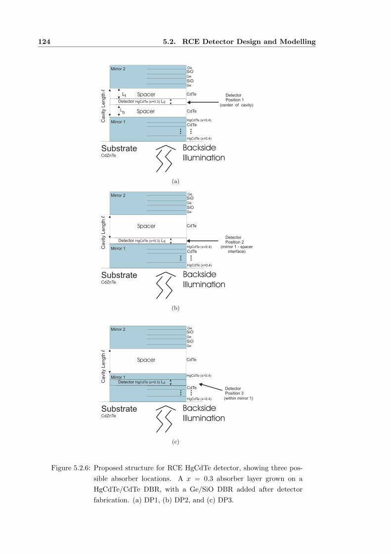
124 5.2. RCE Detector Design and Modelling
Cavity L
ength
l
L
L
t
b
SubstrateCdZnTe
BacksideIllumination
Detector LHgCdTe (x=0.3) d
Mirror 2
Mirror 1
SiOGe
SiOGe
CdTe
HgCdTe (x=0.4)
CdTe
Spacer
Spacer
CdTe
HgCdTe (x=0.4)
Ge
DetectorPosition 1
(center of cavity)
(a)
Ca
vity L
en
gth
l
SubstrateCdZnTe
BacksideIllumination
Detector LHgCdTe (x=0.3) d
Mirror 2
Mirror 1
SiOGe
SiOGe
HgCdTe (x=0.4)
CdTe
Spacer CdTe
HgCdTe (x=0.4)
Ge
DetectorPosition 2
(mirror 1 - spacerinterface)
(b)
Cavity L
ength
l
SubstrateCdZnTe
BacksideIllumination
Detector LHgCdTe (x=0.3) d
Mirror 2
Mirror 1
SiOGe
SiOGe
HgCdTe (x=0.4)
CdTe
Spacer CdTe
HgCdTe (x=0.4)
Ge
DetectorPosition 3
(within mirror 1)
(c)
Figure 5.2.6: Proposed structure for RCE HgCdTe detector, showing three pos-
sible absorber locations. A x = 0.3 absorber layer grown on a
HgCdTe/CdTe DBR, with a Ge/SiO DBR added after detector
fabrication. (a) DP1, (b) DP2, and (c) DP3.
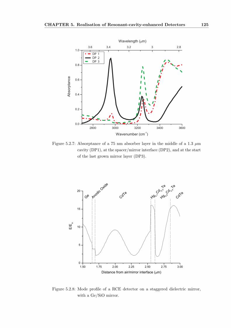
CHAPTER 5. Realisation of Resonant-cavity-enhanced Detectors 125
DP 1
DP 2
DP 3
Figure 5.2.7: Absorptance of a 75 nm absorber layer in the middle of a 1.3 µm
cavity (DP1), at the spacer/mirror interface (DP2), and at the start
of the last grown mirror layer (DP3).
1.50 1.75 2.00 2.25 2.50 2.75 3.000
5
10
15
20
Ge Anodic
Oxid
e
CdTe
CdTe
Hg 0.7Cd 0.3
Te
E/E
in
Distance from air/mirror interface ( m)
Hg 0.6Cd 0.4
Te
Figure 5.2.8: Mode profile of a RCE detector on a staggered dielectric mirror,
with a Ge/SiO mirror.
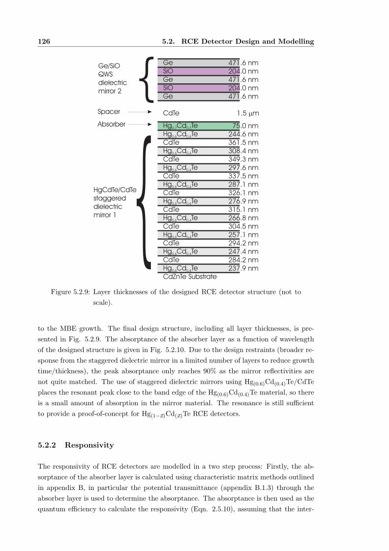
126 5.2. RCE Detector Design and Modelling
237.9 nm284.2 nm247.4 nm294.2 nm257.1 nm304.5 nm266.8 nm315.1 nm276.9 nm326.1 nm287.1 nm337.5 nm297.6 nm349.3 nm308.4 nm361.5 nm244.6 nm
Hg Cd Te0.6 0.4
CdTeHg Cd Te0.6 0.4
Hg Cd Te0.6 0.4
Hg Cd Te0.6 0.4
Hg Cd Te0.6 0.4
Hg Cd Te0.6 0.4
Hg Cd Te0.6 0.4
Hg Cd Te0.6 0.4
Hg Cd Te0.6 0.4
CdTe
CdTe
CdTe
CdTe
CdTe
CdTe
CdTe
CdZnTe Substrate
75.0 nmHg Cd Te0.7 0.3
1.5 mm
GeSiOGeSiO
471.6 nmGe
CdTe
471.6 nm204.0 nm
471.6 nm204.0 nm
HgCdTe/CdTestaggereddielectricmirror 1
Spacer
Absorber
Ge/SiOQWSdielectricmirror 2
Figure 5.2.9: Layer thicknesses of the designed RCE detector structure (not to
scale).
to the MBE growth. The final design structure, including all layer thicknesses, is pre-
sented in Fig. 5.2.9. The absorptance of the absorber layer as a function of wavelength
of the designed structure is given in Fig. 5.2.10. Due to the design restraints (broader re-
sponse from the staggered dielectric mirror in a limited number of layers to reduce growth
time/thickness), the peak absorptance only reaches 90% as the mirror reflectivities are
not quite matched. The use of staggered dielectric mirrors using Hg(0.6)Cd(0.4)Te/CdTe
places the resonant peak close to the band edge of the Hg(0.6)Cd(0.4)Te material, so there
is a small amount of absorption in the mirror material. The resonance is still sufficient
to provide a proof-of-concept for Hg(1−x)Cd(x)Te RCE detectors.
5.2.2 Responsivity
The responsivity of RCE detectors are modelled in a two step process: Firstly, the ab-
sorptance of the absorber layer is calculated using characteristic matrix methods outlined
in appendix B, in particular the potential transmittance (appendix B.1.3) through the
absorber layer is used to determine the absorptance. The absorptance is then used as the
quantum efficiency to calculate the responsivity (Eqn. 2.5.10), assuming that the inter-
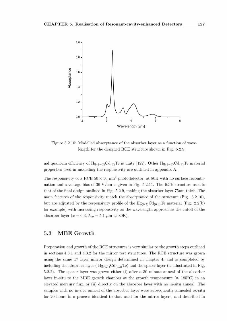
CHAPTER 5. Realisation of Resonant-cavity-enhanced Detectors 127
2 3 4 5 60.0
0.2
0.4
0.6
0.8
1.0
Abs
orptan
ce
Wavelength ( m)
Figure 5.2.10: Modelled absorptance of the absorber layer as a function of wave-
length for the designed RCE structure shown in Fig. 5.2.9.
nal quantum efficiency of Hg(1−x)Cd(x)Te is unity [122]. Other Hg(1−x)Cd(x)Te material
properties used in modelling the responsivity are outlined in appendix A.
The responsivity of a RCE 50 × 50 µm2 photodetector, at 80K with no surface recombi-
nation and a voltage bias of 36 V/cm is given in Fig. 5.2.11. The RCE structure used is
that of the final design outlined in Fig. 5.2.9, making the absorber layer 75nm thick. The
main features of the responsivity match the absorptance of the structure (Fig. 5.2.10),
but are adjusted by the responsivity profile of the Hg(0.7)Cd(0.3)Te material (Fig. 2.2(b)
for example) with increasing responsivity as the wavelength approaches the cutoff of the
absorber layer (x = 0.3, λco = 5.1 µm at 80K).
5.3 MBE Growth
Preparation and growth of the RCE structures is very similar to the growth steps outlined
in sections 4.3.1 and 4.3.2 for the mirror test structures. The RCE structure was grown
using the same 17 layer mirror design determined in chapter 4, and is completed by
including the absorber layer ( Hg(0.7)Cd(0.3)Te) and the spacer layer (as illustrated in Fig.
5.2.2). The spacer layer was grown either (i) after a 30 minute anneal of the absorber
layer in-situ to the MBE growth chamber at the growth temperature (≈ 185C) in an
elevated mercury flux, or (ii) directly on the absorber layer with no in-situ anneal. The
samples with no in-situ anneal of the absorber layer were subsequently annealed ex-situ
for 20 hours in a process identical to that used for the mirror layers, and described in
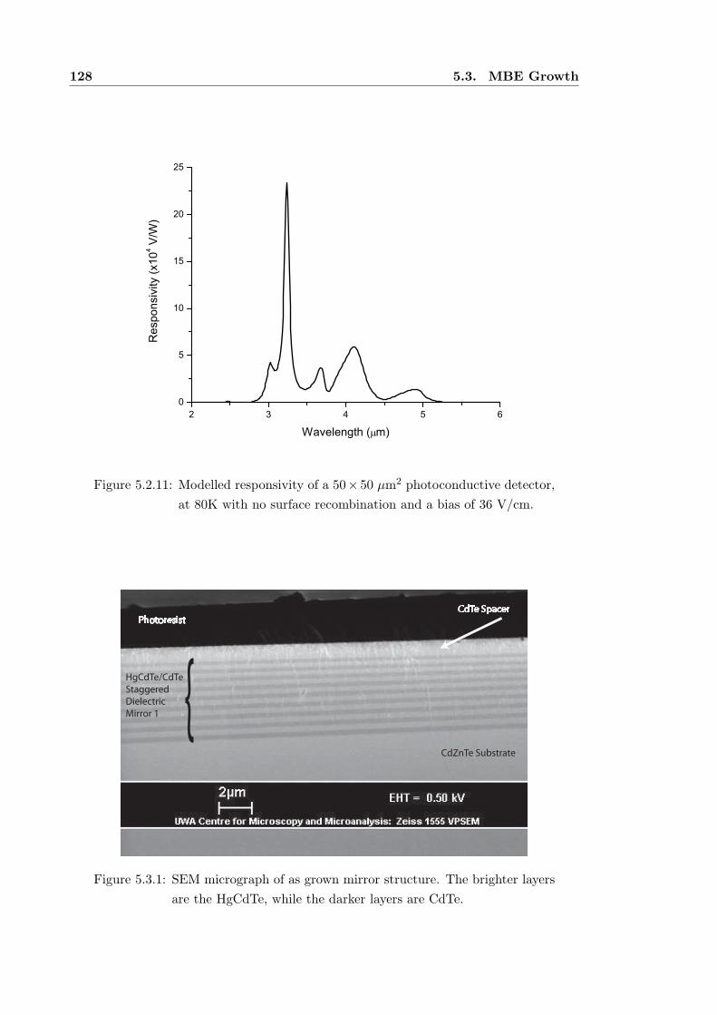
128 5.3. MBE Growth
2 3 4 5 60
5
10
15
20
25R
espo
nsiv
ity (x
104 V
/W)
Wavelength ( m)
Figure 5.2.11: Modelled responsivity of a 50× 50 µm2 photoconductive detector,
at 80K with no surface recombination and a bias of 36 V/cm.
CdTe Spacer
CdZnTe Substrate
HgCdTe/CdTe
Staggered
Dielectric
Mirror 1
Photoresist
Figure 5.3.1: SEM micrograph of as grown mirror structure. The brighter layers
are the HgCdTe, while the darker layers are CdTe.
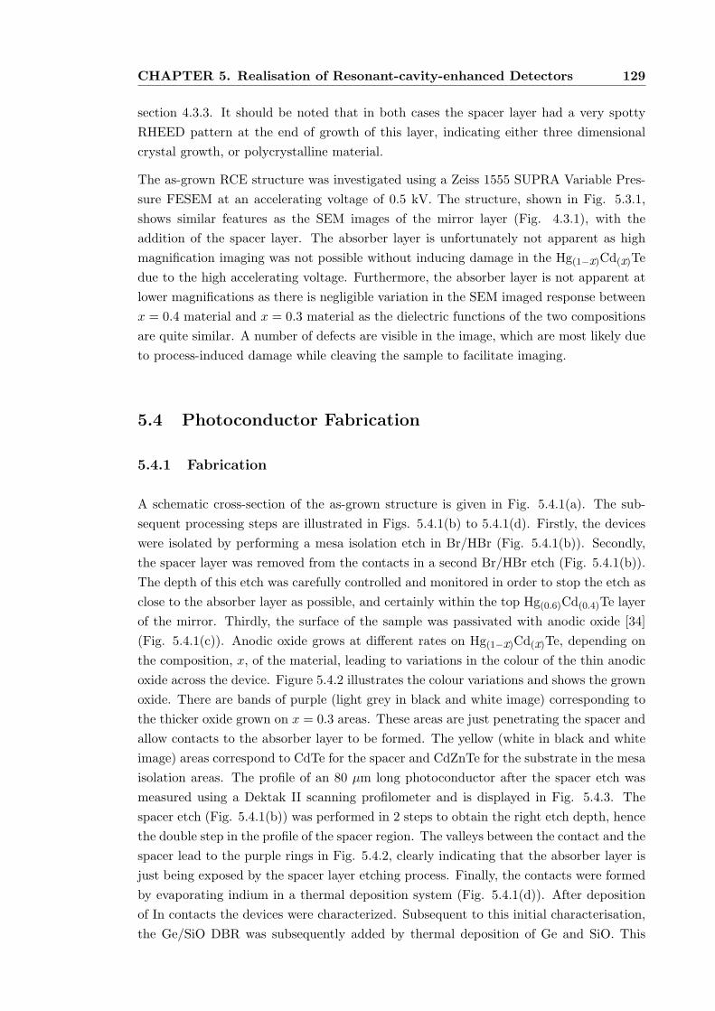
CHAPTER 5. Realisation of Resonant-cavity-enhanced Detectors 129
section 4.3.3. It should be noted that in both cases the spacer layer had a very spotty
RHEED pattern at the end of growth of this layer, indicating either three dimensional
crystal growth, or polycrystalline material.
The as-grown RCE structure was investigated using a Zeiss 1555 SUPRA Variable Pres-
sure FESEM at an accelerating voltage of 0.5 kV. The structure, shown in Fig. 5.3.1,
shows similar features as the SEM images of the mirror layer (Fig. 4.3.1), with the
addition of the spacer layer. The absorber layer is unfortunately not apparent as high
magnification imaging was not possible without inducing damage in the Hg(1−x)Cd(x)Te
due to the high accelerating voltage. Furthermore, the absorber layer is not apparent at
lower magnifications as there is negligible variation in the SEM imaged response between
x = 0.4 material and x = 0.3 material as the dielectric functions of the two compositions
are quite similar. A number of defects are visible in the image, which are most likely due
to process-induced damage while cleaving the sample to facilitate imaging.
5.4 Photoconductor Fabrication
5.4.1 Fabrication
A schematic cross-section of the as-grown structure is given in Fig. 5.4.1(a). The sub-
sequent processing steps are illustrated in Figs. 5.4.1(b) to 5.4.1(d). Firstly, the devices
were isolated by performing a mesa isolation etch in Br/HBr (Fig. 5.4.1(b)). Secondly,
the spacer layer was removed from the contacts in a second Br/HBr etch (Fig. 5.4.1(b)).
The depth of this etch was carefully controlled and monitored in order to stop the etch as
close to the absorber layer as possible, and certainly within the top Hg(0.6)Cd(0.4)Te layer
of the mirror. Thirdly, the surface of the sample was passivated with anodic oxide [34]
(Fig. 5.4.1(c)). Anodic oxide grows at different rates on Hg(1−x)Cd(x)Te, depending on
the composition, x, of the material, leading to variations in the colour of the thin anodic
oxide across the device. Figure 5.4.2 illustrates the colour variations and shows the grown
oxide. There are bands of purple (light grey in black and white image) corresponding to
the thicker oxide grown on x = 0.3 areas. These areas are just penetrating the spacer and
allow contacts to the absorber layer to be formed. The yellow (white in black and white
image) areas correspond to CdTe for the spacer and CdZnTe for the substrate in the mesa
isolation areas. The profile of an 80 µm long photoconductor after the spacer etch was
measured using a Dektak II scanning profilometer and is displayed in Fig. 5.4.3. The
spacer etch (Fig. 5.4.1(b)) was performed in 2 steps to obtain the right etch depth, hence
the double step in the profile of the spacer region. The valleys between the contact and the
spacer lead to the purple rings in Fig. 5.4.2, clearly indicating that the absorber layer is
just being exposed by the spacer layer etching process. Finally, the contacts were formed
by evaporating indium in a thermal deposition system (Fig. 5.4.1(d)). After deposition
of In contacts the devices were characterized. Subsequent to this initial characterisation,
the Ge/SiO DBR was subsequently added by thermal deposition of Ge and SiO. This
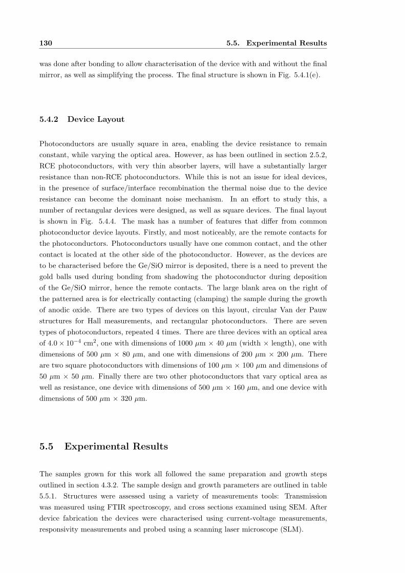
130 5.5. Experimental Results
was done after bonding to allow characterisation of the device with and without the final
mirror, as well as simplifying the process. The final structure is shown in Fig. 5.4.1(e).
5.4.2 Device Layout
Photoconductors are usually square in area, enabling the device resistance to remain
constant, while varying the optical area. However, as has been outlined in section 2.5.2,
RCE photoconductors, with very thin absorber layers, will have a substantially larger
resistance than non-RCE photoconductors. While this is not an issue for ideal devices,
in the presence of surface/interface recombination the thermal noise due to the device
resistance can become the dominant noise mechanism. In an effort to study this, a
number of rectangular devices were designed, as well as square devices. The final layout
is shown in Fig. 5.4.4. The mask has a number of features that differ from common
photoconductor device layouts. Firstly, and most noticeably, are the remote contacts for
the photoconductors. Photoconductors usually have one common contact, and the other
contact is located at the other side of the photoconductor. However, as the devices are
to be characterised before the Ge/SiO mirror is deposited, there is a need to prevent the
gold balls used during bonding from shadowing the photoconductor during deposition
of the Ge/SiO mirror, hence the remote contacts. The large blank area on the right of
the patterned area is for electrically contacting (clamping) the sample during the growth
of anodic oxide. There are two types of devices on this layout, circular Van der Pauw
structures for Hall measurements, and rectangular photoconductors. There are seven
types of photoconductors, repeated 4 times. There are three devices with an optical area
of 4.0× 10⁻⁴ cm2, one with dimensions of 1000 µm × 40 µm (width × length), one with
dimensions of 500 µm × 80 µm, and one with dimensions of 200 µm × 200 µm. There
are two square photoconductors with dimensions of 100 µm × 100 µm and dimensions of
50 µm × 50 µm. Finally there are two other photoconductors that vary optical area as
well as resistance, one device with dimensions of 500 µm × 160 µm, and one device with
dimensions of 500 µm × 320 µm.
5.5 Experimental Results
The samples grown for this work all followed the same preparation and growth steps
outlined in section 4.3.2. The sample design and growth parameters are outlined in table
5.5.1. Structures were assessed using a variety of measurements tools: Transmission
was measured using FTIR spectroscopy, and cross sections examined using SEM. After
device fabrication the devices were characterised using current-voltage measurements,
responsivity measurements and probed using a scanning laser microscope (SLM).
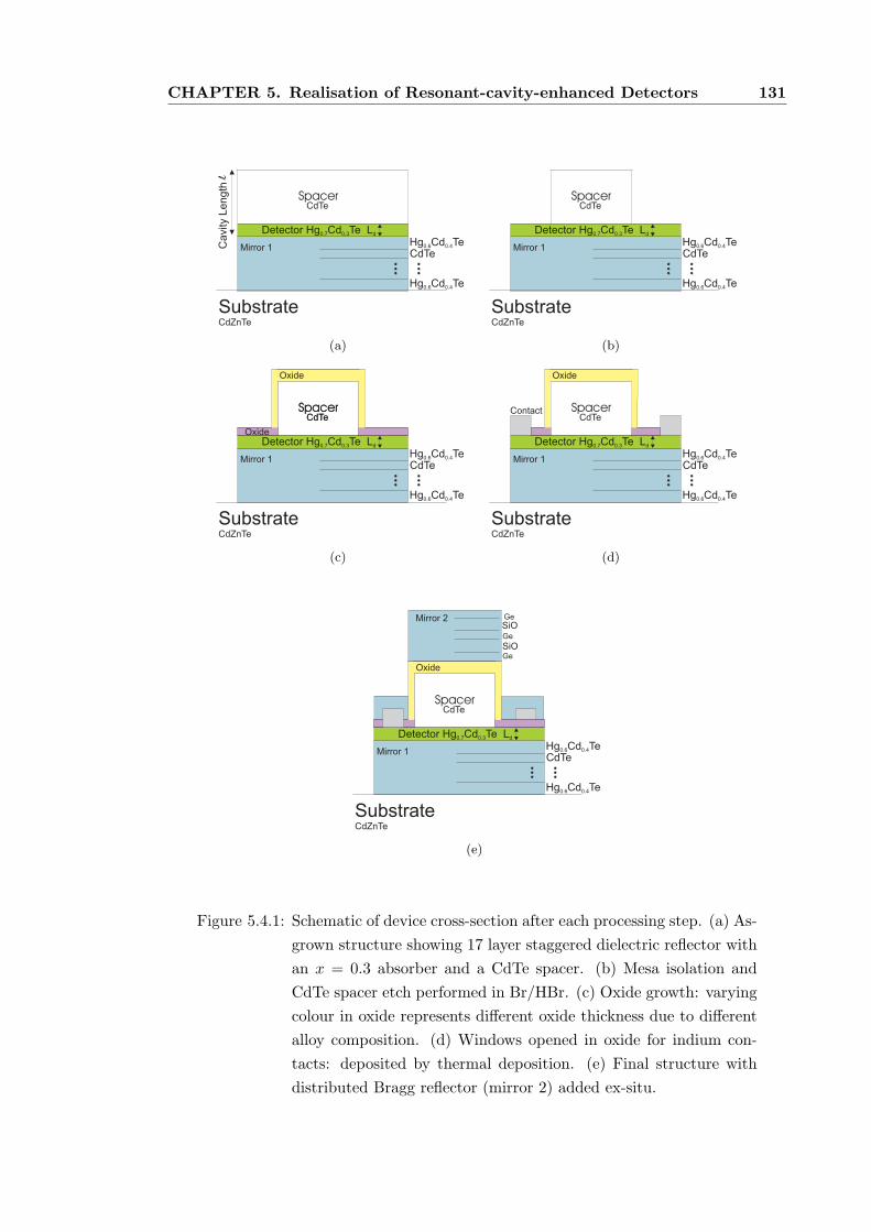
CHAPTER 5. Realisation of Resonant-cavity-enhanced Detectors 131
Ca
vity L
en
gth
l
SubstrateCdZnTe
Mirror 1
SpacerCdTe
Detector Hg Cd Te L0.7 0.3 d
CdTe
Hg Cd Te0.6 0.4
Hg Cd Te0.6 0.4
(a)
SubstrateCdZnTe
Mirror 1
SpacerCdTe
Detector Hg Cd Te L0.7 0.3 d
CdTe
Hg Cd Te0.6 0.4
Hg Cd Te0.6 0.4
(b)
SubstrateCdZnTe
Mirror 1
SpacerCdTe
Detector Hg Cd Te L0.7 0.3 d
CdTe
Hg Cd Te0.6 0.4
Hg Cd Te0.6 0.4
Spacer
Oxide
CdTe
Oxide
(c)
SubstrateCdZnTe
Mirror 1
Spacer
Oxide
ContactCdTe
Detector Hg Cd Te L0.7 0.3 d
CdTe
Hg Cd Te0.6 0.4
Hg Cd Te0.6 0.4
(d)
SubstrateCdZnTe
Detector Hg Cd Te L0.7 0.3 d
Mirror 1CdTe
Mirror 2SiOGe
SiOGe
Ge
Hg Cd Te0.6 0.4
Hg Cd Te0.6 0.4
Spacer
Oxide
CdTe
(e)
Figure 5.4.1: Schematic of device cross-section after each processing step. (a) As-
grown structure showing 17 layer staggered dielectric reflector with
an x = 0.3 absorber and a CdTe spacer. (b) Mesa isolation and
CdTe spacer etch performed in Br/HBr. (c) Oxide growth: varying
colour in oxide represents different oxide thickness due to different
alloy composition. (d) Windows opened in oxide for indium con-
tacts: deposited by thermal deposition. (e) Final structure with
distributed Bragg reflector (mirror 2) added ex-situ.
132 5.5. Experimental Results
Figure 5.4.2: 50×50µm2 photoconductor after anodic oxide is grown, and before
indium contacts are added. Anodic oxide on CdTe (and on CdZnTe
substrate) is yellow in colour (white), while anodic oxide grown on
Hg(0.7)Cd(0.3)Te is purple in colour (light grey).
0 50 100 150 2000
2
4
6
8Contact
Hei
ght (
m)
X position ( m)
Spacer Contact
Figure 5.4.3: Topographical profile of 80 × 500µm2 photoconductor after the
spacer layer has been etched.
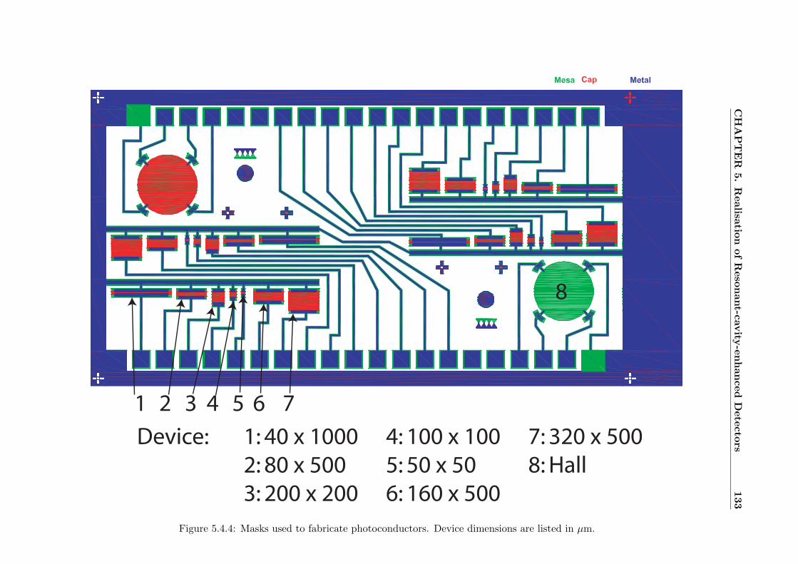
CH
AP
TER
5.
Realisa
tion
ofR
eso
nant-c
avity
-enhanced
Dete
cto
rs133
8
1 2 3 4 5 6 7
Device: 1: 40 x 1000 4: 100 x 100 7: 320 x 500
2: 80 x 500 5: 50 x 50 8: Hall
3: 200 x 200 6: 160 x 500
Figure 5.4.4: Masks used to fabricate photoconductors. Device dimensions are listed in µm.
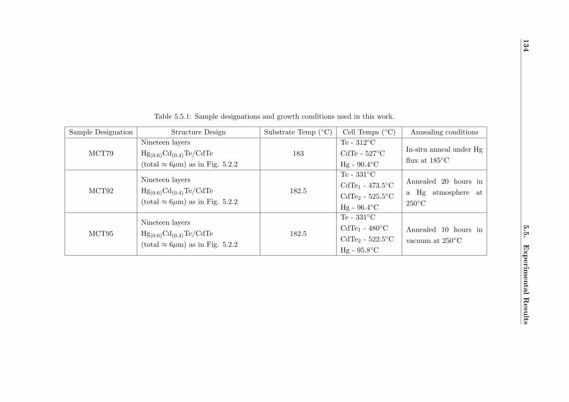
134
5.5
.Experim
enta
lR
esu
lts
Table 5.5.1: Sample designations and growth conditions used in this work.
Sample Designation Structure Design Substrate Temp (C) Cell Temps (C) Annealing conditions
MCT79
Nineteen layers
Hg(0.6)Cd(0.4)Te/CdTe
(total ≈ 6µm) as in Fig. 5.2.2
183
Te - 312C
CdTe - 527C
Hg - 90.4C
In-situ anneal under Hg
flux at 185C
MCT92
Nineteen layers
Hg(0.6)Cd(0.4)Te/CdTe
(total ≈ 6µm) as in Fig. 5.2.2
182.5
Te - 331C
CdTe1 - 473.5C
CdTe2 - 525.5C
Hg - 96.4C
Annealed 20 hours in
a Hg atmosphere at
250C
MCT95
Nineteen layers
Hg(0.6)Cd(0.4)Te/CdTe
(total ≈ 6µm) as in Fig. 5.2.2
182.5
Te - 331C
CdTe1 - 480C
CdTe2 - 522.5C
Hg - 95.8C
Annealed 10 hours in
vacuum at 250C
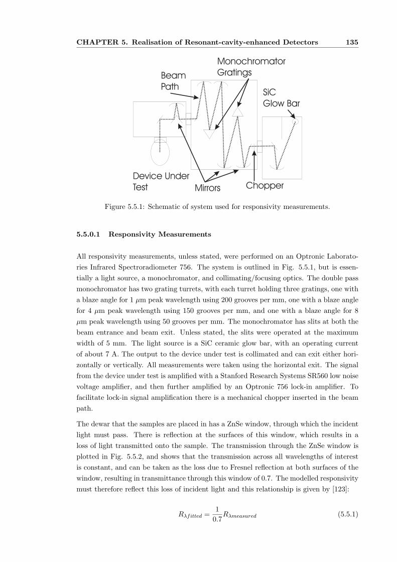
CHAPTER 5. Realisation of Resonant-cavity-enhanced Detectors 135
SiCGlow Bar
Mirrors
BeamPath
Device UnderTest
MonochromatorGratings
Chopper
Figure 5.5.1: Schematic of system used for responsivity measurements.
5.5.0.1 Responsivity Measurements
All responsivity measurements, unless stated, were performed on an Optronic Laborato-
ries Infrared Spectroradiometer 756. The system is outlined in Fig. 5.5.1, but is essen-
tially a light source, a monochromator, and collimating/focusing optics. The double pass
monochromator has two grating turrets, with each turret holding three gratings, one with
a blaze angle for 1 µm peak wavelength using 200 grooves per mm, one with a blaze angle
for 4 µm peak wavelength using 150 grooves per mm, and one with a blaze angle for 8
µm peak wavelength using 50 grooves per mm. The monochromator has slits at both the
beam entrance and beam exit. Unless stated, the slits were operated at the maximum
width of 5 mm. The light source is a SiC ceramic glow bar, with an operating current
of about 7 A. The output to the device under test is collimated and can exit either hori-
zontally or vertically. All measurements were taken using the horizontal exit. The signal
from the device under test is amplified with a Stanford Research Systems SR560 low noise
voltage amplifier, and then further amplified by an Optronic 756 lock-in amplifier. To
facilitate lock-in signal amplification there is a mechanical chopper inserted in the beam
path.
The dewar that the samples are placed in has a ZnSe window, through which the incident
light must pass. There is reflection at the surfaces of this window, which results in a
loss of light transmitted onto the sample. The transmission through the ZnSe window is
plotted in Fig. 5.5.2, and shows that the transmission across all wavelengths of interest
is constant, and can be taken as the loss due to Fresnel reflection at both surfaces of the
window, resulting in transmittance through this window of 0.7. The modelled responsivity
must therefore reflect this loss of incident light and this relationship is given by [123]:
Rλfitted =1
0.7Rλmeasured (5.5.1)
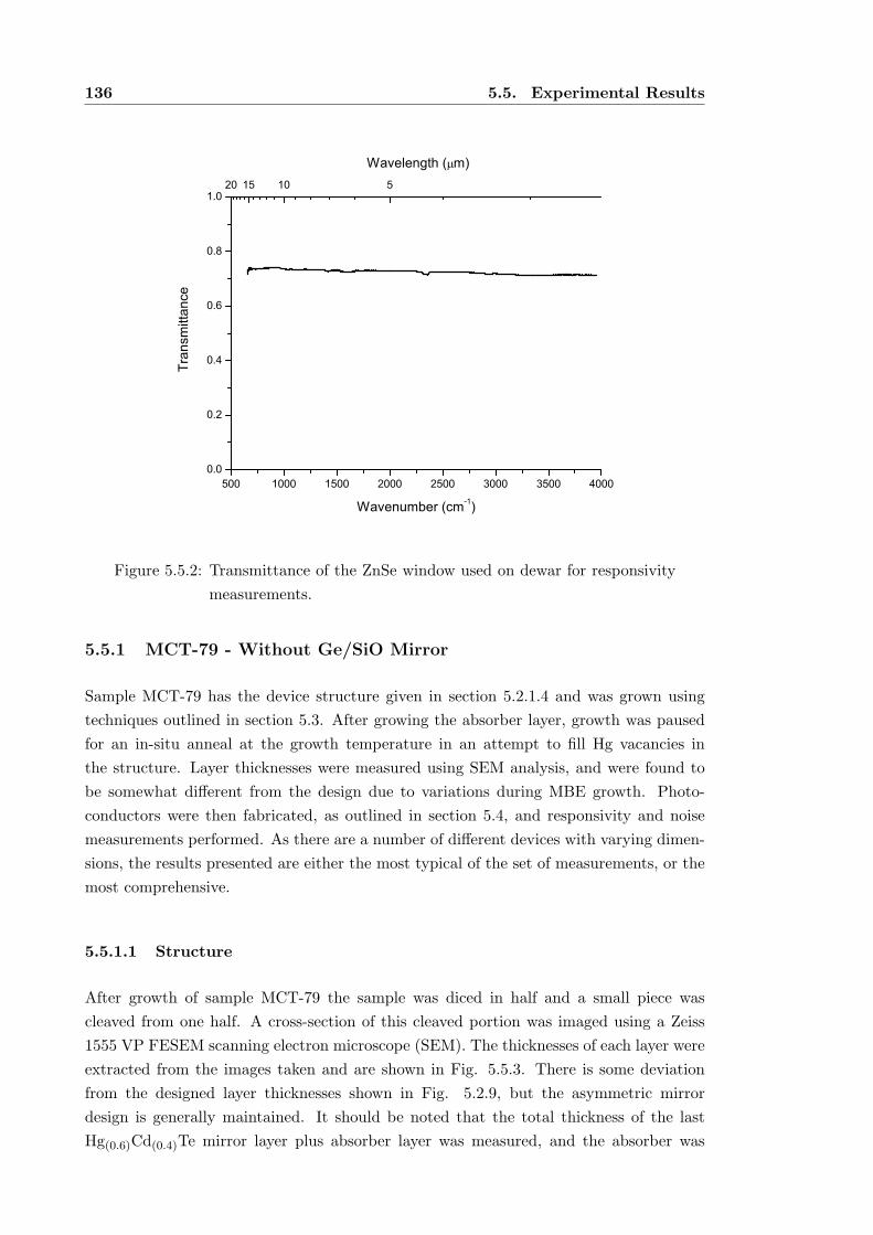
136 5.5. Experimental Results
500 1000 1500 2000 2500 3000 3500 40000.0
0.2
0.4
0.6
0.8
1.020 15 10 5
Tran
smittan
ce
Wavenumber (cm-1)
Wavelength ( m)
Figure 5.5.2: Transmittance of the ZnSe window used on dewar for responsivity
measurements.
5.5.1 MCT-79 - Without Ge/SiO Mirror
Sample MCT-79 has the device structure given in section 5.2.1.4 and was grown using
techniques outlined in section 5.3. After growing the absorber layer, growth was paused
for an in-situ anneal at the growth temperature in an attempt to fill Hg vacancies in
the structure. Layer thicknesses were measured using SEM analysis, and were found to
be somewhat different from the design due to variations during MBE growth. Photo-
conductors were then fabricated, as outlined in section 5.4, and responsivity and noise
measurements performed. As there are a number of different devices with varying dimen-
sions, the results presented are either the most typical of the set of measurements, or the
most comprehensive.
5.5.1.1 Structure
After growth of sample MCT-79 the sample was diced in half and a small piece was
cleaved from one half. A cross-section of this cleaved portion was imaged using a Zeiss
1555 VP FESEM scanning electron microscope (SEM). The thicknesses of each layer were
extracted from the images taken and are shown in Fig. 5.5.3. There is some deviation
from the designed layer thicknesses shown in Fig. 5.2.9, but the asymmetric mirror
design is generally maintained. It should be noted that the total thickness of the last
Hg(0.6)Cd(0.4)Te mirror layer plus absorber layer was measured, and the absorber was
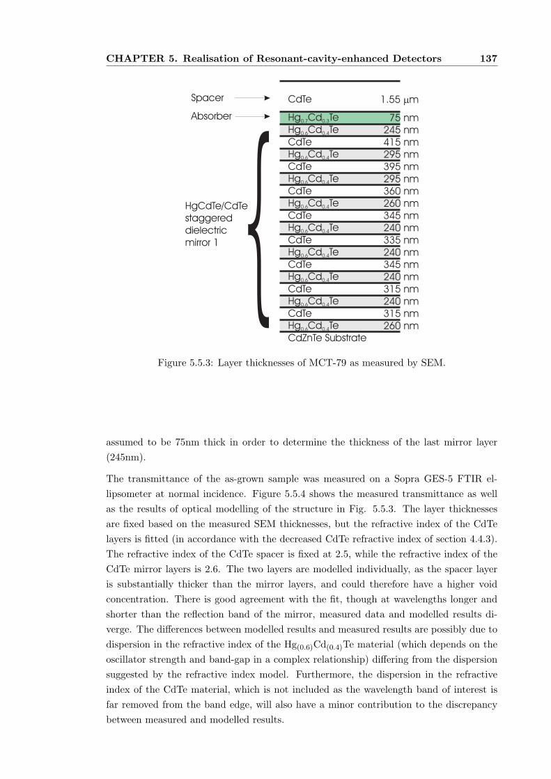
CHAPTER 5. Realisation of Resonant-cavity-enhanced Detectors 137
260 nm315 nm240 nm315 nm240 nm345 nm240 nm335 nm240 nm345 nm260 nm360 nm295 nm395 nm295 nm415 nm245 nm
Hg Cd Te0.6 0.4
CdTeHg Cd Te0.6 0.4
Hg Cd Te0.6 0.4
Hg Cd Te0.6 0.4
Hg Cd Te0.6 0.4
Hg Cd Te0.6 0.4
Hg Cd Te0.6 0.4
Hg Cd Te0.6 0.4
Hg Cd Te0.6 0.4
CdTe
CdTe
CdTe
CdTe
CdTe
CdTe
CdTe
CdZnTe Substrate
75 nmHg Cd Te0.7 0.3
1.55 mmCdTe
HgCdTe/CdTestaggereddielectricmirror 1
Spacer
Absorber
Figure 5.5.3: Layer thicknesses of MCT-79 as measured by SEM.
assumed to be 75nm thick in order to determine the thickness of the last mirror layer
(245nm).
The transmittance of the as-grown sample was measured on a Sopra GES-5 FTIR el-
lipsometer at normal incidence. Figure 5.5.4 shows the measured transmittance as well
as the results of optical modelling of the structure in Fig. 5.5.3. The layer thicknesses
are fixed based on the measured SEM thicknesses, but the refractive index of the CdTe
layers is fitted (in accordance with the decreased CdTe refractive index of section 4.4.3).
The refractive index of the CdTe spacer is fixed at 2.5, while the refractive index of the
CdTe mirror layers is 2.6. The two layers are modelled individually, as the spacer layer
is substantially thicker than the mirror layers, and could therefore have a higher void
concentration. There is good agreement with the fit, though at wavelengths longer and
shorter than the reflection band of the mirror, measured data and modelled results di-
verge. The differences between modelled results and measured results are possibly due to
dispersion in the refractive index of the Hg(0.6)Cd(0.4)Te material (which depends on the
oscillator strength and band-gap in a complex relationship) differing from the dispersion
suggested by the refractive index model. Furthermore, the dispersion in the refractive
index of the CdTe material, which is not included as the wavelength band of interest is
far removed from the band edge, will also have a minor contribution to the discrepancy
between measured and modelled results.
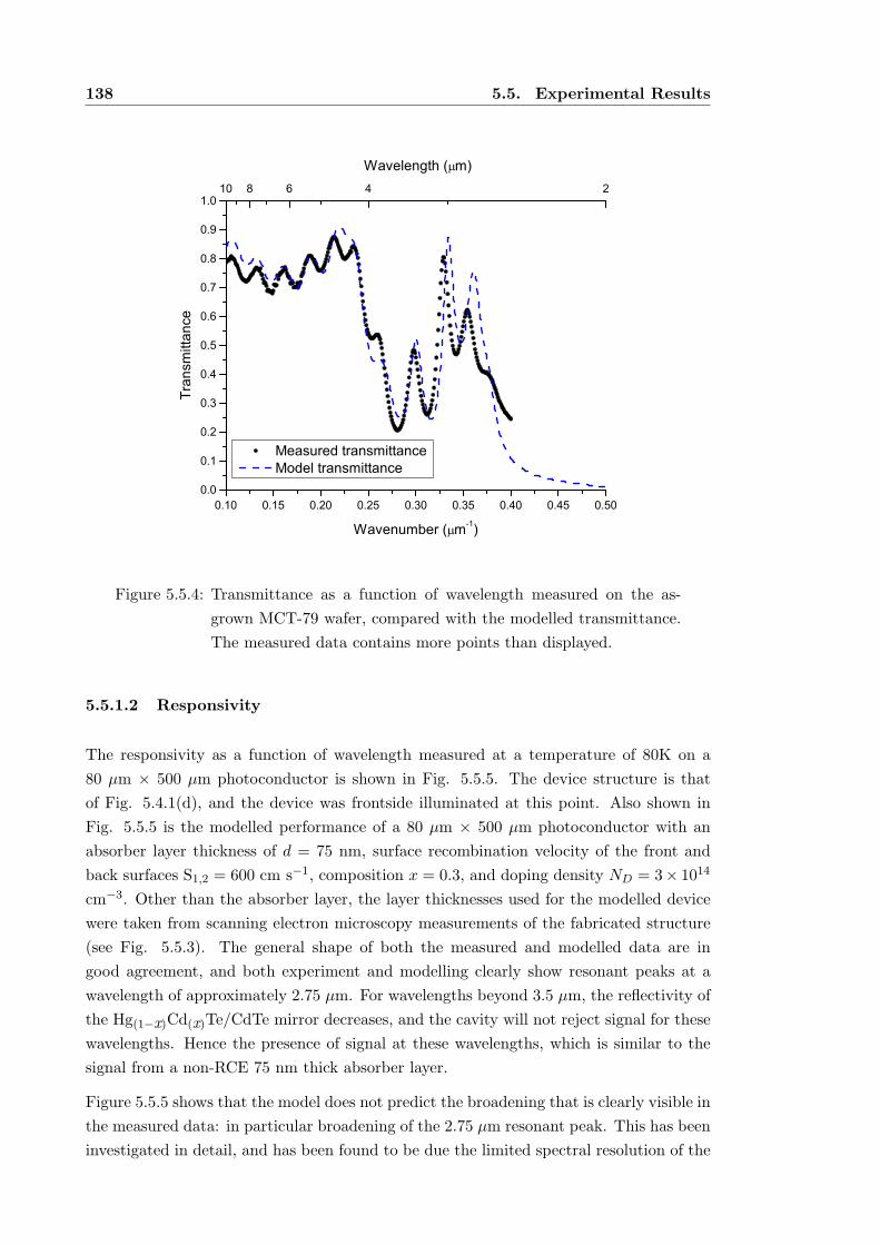
138 5.5. Experimental Results
0.10 0.15 0.20 0.25 0.30 0.35 0.40 0.45 0.500.0
0.1
0.2
0.3
0.4
0.5
0.6
0.7
0.8
0.9
1.010 8 6 4 2
Measured transmittance Model transmittance
Tran
smittan
ce
Wavenumber ( m-1)
Wavelength ( m)
Figure 5.5.4: Transmittance as a function of wavelength measured on the as-
grown MCT-79 wafer, compared with the modelled transmittance.
The measured data contains more points than displayed.
5.5.1.2 Responsivity
The responsivity as a function of wavelength measured at a temperature of 80K on a
80 µm × 500 µm photoconductor is shown in Fig. 5.5.5. The device structure is that
of Fig. 5.4.1(d), and the device was frontside illuminated at this point. Also shown in
Fig. 5.5.5 is the modelled performance of a 80 µm × 500 µm photoconductor with an
absorber layer thickness of d = 75 nm, surface recombination velocity of the front and
back surfaces S1,2 = 600 cm s−1, composition x = 0.3, and doping density ND = 3× 10¹⁴
cm−3. Other than the absorber layer, the layer thicknesses used for the modelled device
were taken from scanning electron microscopy measurements of the fabricated structure
(see Fig. 5.5.3). The general shape of both the measured and modelled data are in
good agreement, and both experiment and modelling clearly show resonant peaks at a
wavelength of approximately 2.75 µm. For wavelengths beyond 3.5 µm, the reflectivity of
the Hg(1−x)Cd(x)Te/CdTe mirror decreases, and the cavity will not reject signal for these
wavelengths. Hence the presence of signal at these wavelengths, which is similar to the
signal from a non-RCE 75 nm thick absorber layer.
Figure 5.5.5 shows that the model does not predict the broadening that is clearly visible in
the measured data: in particular broadening of the 2.75 µm resonant peak. This has been
investigated in detail, and has been found to be due the limited spectral resolution of the
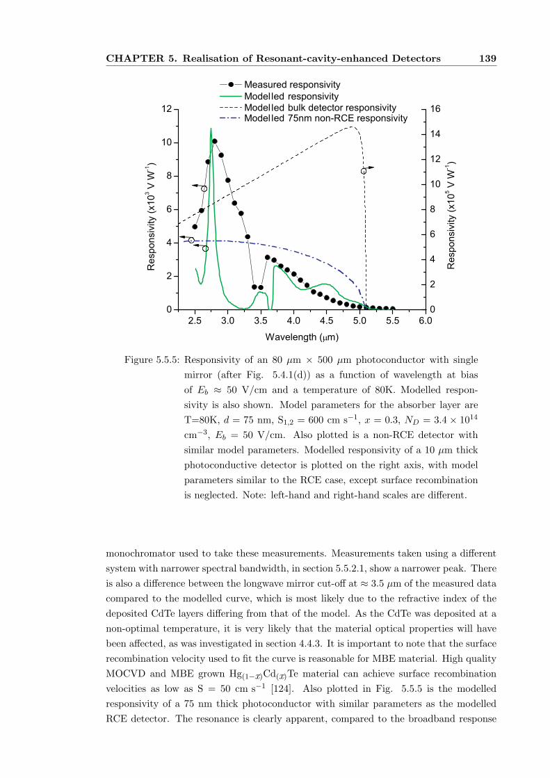
CHAPTER 5. Realisation of Resonant-cavity-enhanced Detectors 139
Figure 5.5.5: Responsivity of an 80 µm × 500 µm photoconductor with single
mirror (after Fig. 5.4.1(d)) as a function of wavelength at bias
of Eb ≈ 50 V/cm and a temperature of 80K. Modelled respon-
sivity is also shown. Model parameters for the absorber layer are
T=80K, d = 75 nm, S1,2 = 600 cm s−1, x = 0.3, ND = 3.4 × 10¹⁴
cm−3, Eb = 50 V/cm. Also plotted is a non-RCE detector with
similar model parameters. Modelled responsivity of a 10 µm thick
photoconductive detector is plotted on the right axis, with model
parameters similar to the RCE case, except surface recombination
is neglected. Note: left-hand and right-hand scales are different.
monochromator used to take these measurements. Measurements taken using a different
system with narrower spectral bandwidth, in section 5.5.2.1, show a narrower peak. There
is also a difference between the longwave mirror cut-off at ≈ 3.5 µm of the measured data
compared to the modelled curve, which is most likely due to the refractive index of the
deposited CdTe layers differing from that of the model. As the CdTe was deposited at a
non-optimal temperature, it is very likely that the material optical properties will have
been affected, as was investigated in section 4.4.3. It is important to note that the surface
recombination velocity used to fit the curve is reasonable for MBE material. High quality
MOCVD and MBE grown Hg(1−x)Cd(x)Te material can achieve surface recombination
velocities as low as S = 50 cm s−1 [124]. Also plotted in Fig. 5.5.5 is the modelled
responsivity of a 75 nm thick photoconductor with similar parameters as the modelled
RCE detector. The resonance is clearly apparent, compared to the broadband response
140 5.5. Experimental Results
of the non-RCE detector. Furthermore, the increase in performance for the RCE detector
is apparent as the resonant peak has a responsivity of 10×103 V/W, while the non-RCE
detector only achieves a peak responsivity of 4×10³ V/W. Finally, plotted in Fig. 5.5.5 is
the modelled response of a bulk photoconductor, with the same parameters as the RCE
photoconductor, but neglecting surface recombination, which will have negligible effect
on the lifetime for a bulk photoconductor. The modelled peak responsivity of the bulk
photoconductor is approximately two orders of magnitude larger than that of the RCE
detector. This is due to the surface recombination dominating the lifetime of the RCE
detector and severely limiting performance. The resonant nature of the RCE detector is
also apparent when compared with the responsivity of a bulk photoconductor, which has
no resonant peaks.
5.5.1.3 Varying Temperature
By varying the measurement temperature, further material properties can be investigated.
Figure 5.5.6 illustrates the normalized responsivity of a 80 µm × 500 µm photoconductor
at temperatures of 80K and 250K. These are compared with the modelled normalized
responsivity for a 10 µm thick detector at 80K and 250K. There is very good agreement in
the shift in cut-off due to the changing band-gap of the Hg(1−x)Cd(x)Te with temperature.
This is apparent as the signal in the mirror roll-off region (3.5 - 5 µm) experiences a shift
in cut-off. The responsivity at 250K clearly drops to the noise floor of the measurement
set up after 4.4 µm. The cut-off at 80K is more difficult to determine, as a traditional
half-peak responsivity [62] analysis cannot be used since the signal does not cut out as
sharply as in the 250K case. Figure 5.5.5 shows good agreement between the modelled
responsivity and measured responsivity at longer wavelengths, and as the composition
used for the modelled RCE detector is the same for the bulk photoconductor and the
cutoff wavelength as a function of composition is very well defined, it can be inferred that
the cutoff at 80K is accurate as modelled. The peak responsivity shifts in wavelength
due to the change in refractive index with temperature, but this effect results in only a
100 nm change in the peak responsivity since the resonance is primarily controlled by the
optical length of the cavity and phase change in the mirrors, which are in turn controlled
by the refractive index of the materials. The effect of the change in refractive index as a
function of temperature is small compared to the change in energy gap.
Peak responsivity of a 50 µm × 50 µm RCE photoconductor was also measured for
varying temperatures for a fixed bias field of Eb ≈ 36 V/cm, with the results shown
in Fig. 5.5.7. Above 200K, the peak responsivity is highly dependant on the intrinsic
carrier concentration, as the carrier concentration is a function of temperature and the
narrow band-gap means that the intrinsic carrier concentration can become quite large
even at moderately low temperatures. Below 200K, the responsivity is independent of
temperature since the dominant lifetime mechanism is surface recombination. Despite
the relatively low value of fitted surface recombination of S1,2 = 200 cm s−1, surface
recombination becomes the dominant mechanism limiting the lifetime, and hence the
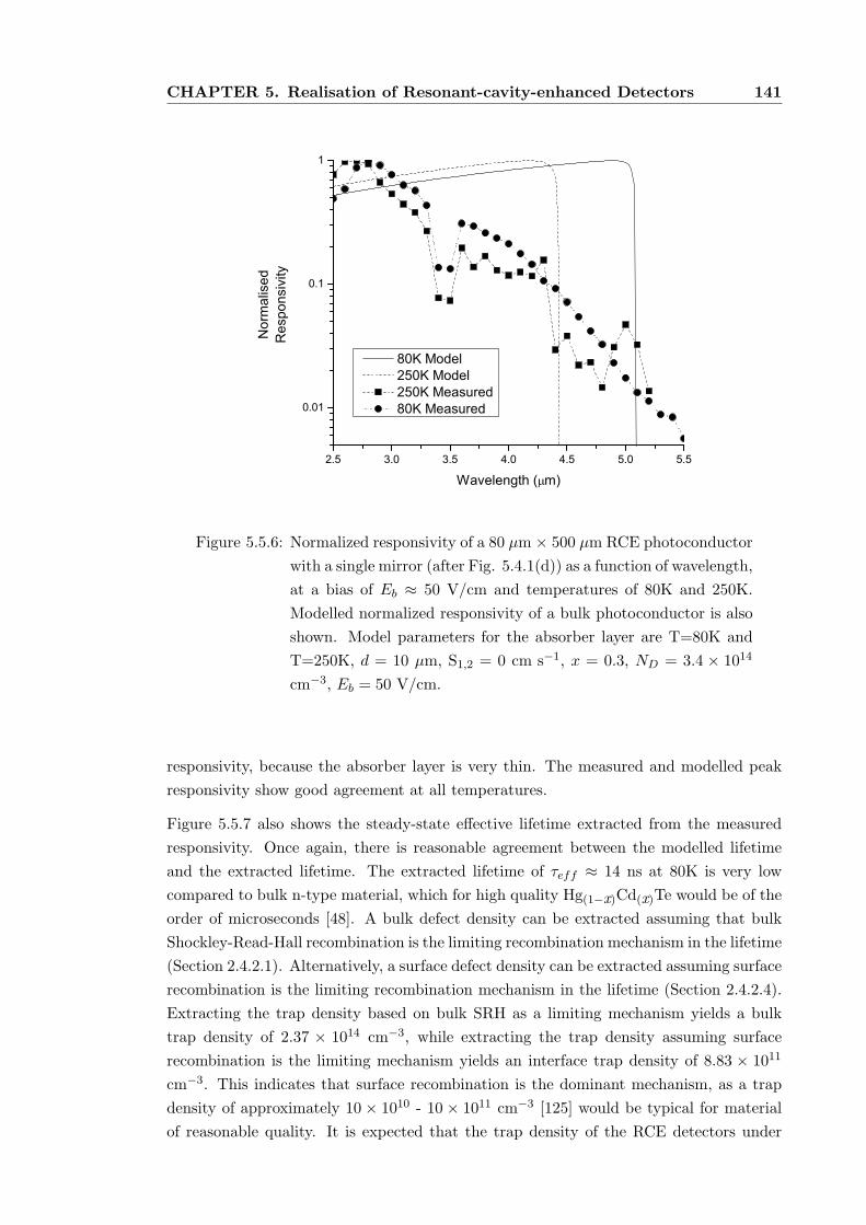
CHAPTER 5. Realisation of Resonant-cavity-enhanced Detectors 141
2.5 3.0 3.5 4.0 4.5 5.0 5.5
0.01
0.1
1
Normalised
Res
pons
ivity
Wavelength ( m)
80K Model 250K Model 250K Measured 80K Measured
Figure 5.5.6: Normalized responsivity of a 80 µm × 500 µm RCE photoconductor
with a single mirror (after Fig. 5.4.1(d)) as a function of wavelength,
at a bias of Eb ≈ 50 V/cm and temperatures of 80K and 250K.
Modelled normalized responsivity of a bulk photoconductor is also
shown. Model parameters for the absorber layer are T=80K and
T=250K, d = 10 µm, S1,2 = 0 cm s−1, x = 0.3, ND = 3.4 × 10¹⁴
cm−3, Eb = 50 V/cm.
responsivity, because the absorber layer is very thin. The measured and modelled peak
responsivity show good agreement at all temperatures.
Figure 5.5.7 also shows the steady-state effective lifetime extracted from the measured
responsivity. Once again, there is reasonable agreement between the modelled lifetime
and the extracted lifetime. The extracted lifetime of τeff ≈ 14 ns at 80K is very low
compared to bulk n-type material, which for high quality Hg(1−x)Cd(x)Te would be of the
order of microseconds [48]. A bulk defect density can be extracted assuming that bulk
Shockley-Read-Hall recombination is the limiting recombination mechanism in the lifetime
(Section 2.4.2.1). Alternatively, a surface defect density can be extracted assuming surface
recombination is the limiting recombination mechanism in the lifetime (Section 2.4.2.4).
Extracting the trap density based on bulk SRH as a limiting mechanism yields a bulk
trap density of 2.37 × 1014 cm−3, while extracting the trap density assuming surface
recombination is the limiting mechanism yields an interface trap density of 8.83 × 10¹¹
cm−3. This indicates that surface recombination is the dominant mechanism, as a trap
density of approximately 10 × 1010 - 10 × 1011 cm−3 [125] would be typical for material
of reasonable quality. It is expected that the trap density of the RCE detectors under
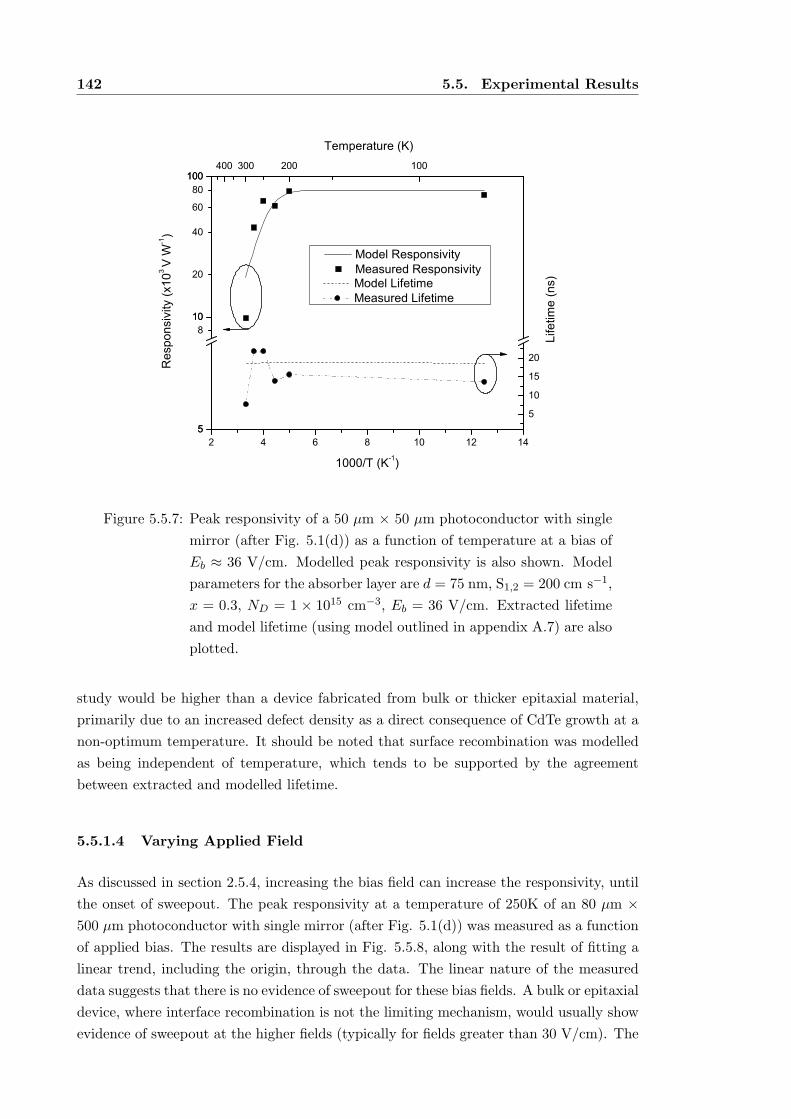
142 5.5. Experimental Results
2 4 6 8 10 12 1455
81010
20
40
60
80100100
400 300 200 100
5
10
15
20Res
pons
ivity
(x10
3 V
W-1)
1000/T (K-1)
Model Responsivity Measured Responsivity
Temperature (K)
Life
time
(ns) Model Lifetime
Measured Lifetime
Figure 5.5.7: Peak responsivity of a 50 µm × 50 µm photoconductor with single
mirror (after Fig. 5.1(d)) as a function of temperature at a bias of
Eb ≈ 36 V/cm. Modelled peak responsivity is also shown. Model
parameters for the absorber layer are d = 75 nm, S1,2 = 200 cm s−1,
x = 0.3, ND = 1 × 1015 cm−3, Eb = 36 V/cm. Extracted lifetime
and model lifetime (using model outlined in appendix A.7) are also
plotted.
study would be higher than a device fabricated from bulk or thicker epitaxial material,
primarily due to an increased defect density as a direct consequence of CdTe growth at a
non-optimum temperature. It should be noted that surface recombination was modelled
as being independent of temperature, which tends to be supported by the agreement
between extracted and modelled lifetime.
5.5.1.4 Varying Applied Field
As discussed in section 2.5.4, increasing the bias field can increase the responsivity, until
the onset of sweepout. The peak responsivity at a temperature of 250K of an 80 µm ×500 µm photoconductor with single mirror (after Fig. 5.1(d)) was measured as a function
of applied bias. The results are displayed in Fig. 5.5.8, along with the result of fitting a
linear trend, including the origin, through the data. The linear nature of the measured
data suggests that there is no evidence of sweepout for these bias fields. A bulk or epitaxial
device, where interface recombination is not the limiting mechanism, would usually show
evidence of sweepout at the higher fields (typically for fields greater than 30 V/cm). The
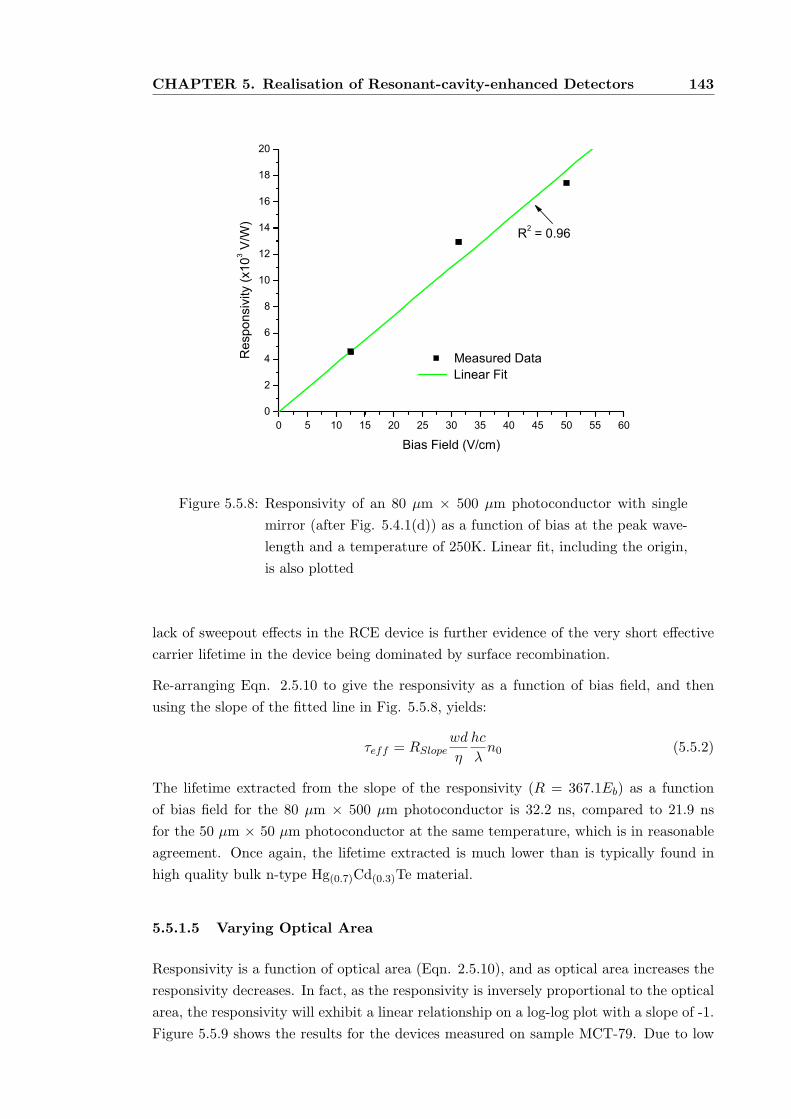
CHAPTER 5. Realisation of Resonant-cavity-enhanced Detectors 143
0 5 10 15 20 25 30 35 40 45 50 55 600
2
4
6
8
10
12
14
16
18
20
R2 = 0.96
Linear Fit
Res
pons
ivity
(x10
3 V/W
)
Bias Field (V/cm)
Measured Data
Figure 5.5.8: Responsivity of an 80 µm × 500 µm photoconductor with single
mirror (after Fig. 5.4.1(d)) as a function of bias at the peak wave-
length and a temperature of 250K. Linear fit, including the origin,
is also plotted
lack of sweepout effects in the RCE device is further evidence of the very short effective
carrier lifetime in the device being dominated by surface recombination.
Re-arranging Eqn. 2.5.10 to give the responsivity as a function of bias field, and then
using the slope of the fitted line in Fig. 5.5.8, yields:
τeff = RSlopewd
η
hc
λn0 (5.5.2)
The lifetime extracted from the slope of the responsivity (R = 367.1Eb) as a function
of bias field for the 80 µm × 500 µm photoconductor is 32.2 ns, compared to 21.9 ns
for the 50 µm × 50 µm photoconductor at the same temperature, which is in reasonable
agreement. Once again, the lifetime extracted is much lower than is typically found in
high quality bulk n-type Hg(0.7)Cd(0.3)Te material.
5.5.1.5 Varying Optical Area
Responsivity is a function of optical area (Eqn. 2.5.10), and as optical area increases the
responsivity decreases. In fact, as the responsivity is inversely proportional to the optical
area, the responsivity will exhibit a linear relationship on a log-log plot with a slope of -1.
Figure 5.5.9 shows the results for the devices measured on sample MCT-79. Due to low
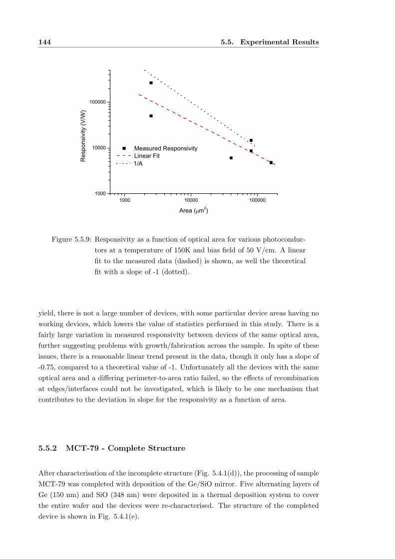
144 5.5. Experimental Results
1000 10000 1000001000
10000
100000
Measured Responsivity Linear Fit
Res
pons
ivity
(V/W
)
Area ( m2)
1/A
Figure 5.5.9: Responsivity as a function of optical area for various photoconduc-
tors at a temperature of 150K and bias field of 50 V/cm. A linear
fit to the measured data (dashed) is shown, as well the theoretical
fit with a slope of -1 (dotted).
yield, there is not a large number of devices, with some particular device areas having no
working devices, which lowers the value of statistics performed in this study. There is a
fairly large variation in measured responsivity between devices of the same optical area,
further suggesting problems with growth/fabrication across the sample. In spite of these
issues, there is a reasonable linear trend present in the data, though it only has a slope of
-0.75, compared to a theoretical value of -1. Unfortunately all the devices with the same
optical area and a differing perimeter-to-area ratio failed, so the effects of recombination
at edges/interfaces could not be investigated, which is likely to be one mechanism that
contributes to the deviation in slope for the responsivity as a function of area.
5.5.2 MCT-79 - Complete Structure
After characterisation of the incomplete structure (Fig. 5.4.1(d)), the processing of sample
MCT-79 was completed with deposition of the Ge/SiO mirror. Five alternating layers of
Ge (150 nm) and SiO (348 nm) were deposited in a thermal deposition system to cover
the entire wafer and the devices were re-characterised. The structure of the completed
device is shown in Fig. 5.4.1(e).
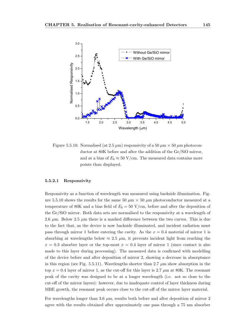
CHAPTER 5. Realisation of Resonant-cavity-enhanced Detectors 145
1.5 2.0 2.5 3.0 3.5 4.0 4.5 5.00.0
0.5
1.0
1.5
2.0
2.5
3.0
Nor
mal
ised
Res
pons
ivity
Wavelength ( m)
Without Ge/SiO mirror With Ge/SiO mirror
Figure 5.5.10: Normalised (at 2.5 µm) responsivity of a 50 µm × 50 µm photocon-
ductor at 80K before and after the addition of the Ge/SiO mirror,
and at a bias of Eb ≈ 50 V/cm. The measured data contains more
points than displayed.
5.5.2.1 Responsivity
Responsivity as a function of wavelength was measured using backside illumination. Fig-
ure 5.5.10 shows the results for the same 50 µm × 50 µm photoconductor measured at a
temperature of 80K and a bias field of Eb = 50 V/cm, before and after the deposition of
the Ge/SiO mirror. Both data sets are normalised to the responsivity at a wavelength of
2.6 µm. Below 2.5 µm there is a marked difference between the two curves. This is due
to the fact that, as the device is now backside illuminated, and incident radiation must
pass through mirror 1 before entering the cavity. As the x = 0.4 material of mirror 1 is
absorbing at wavelengths below ≈ 2.5 µm, it prevents incident light from reaching the
x = 0.3 absorber layer or the top-most x = 0.4 layer of mirror 1 (since contact is also
made to this layer during processing). The measured data is confirmed with modelling
of the device before and after deposition of mirror 2, showing a decrease in absorptance
in this region (see Fig. 5.5.11). Wavelengths shorter than 2.7 µm show absorption in the
top x = 0.4 layer of mirror 1, as the cut-off for this layer is 2.7 µm at 80K. The resonant
peak of the cavity was designed to be at a longer wavelength (i.e. not so close to the
cut-off of the mirror layers): however, due to inadequate control of layer thickness during
MBE growth, the resonant peak occurs close to the cut-off of the mirror layer material.
For wavelengths longer than 3.6 µm, results both before and after deposition of mirror 2
agree with the results obtained after approximately one pass through a 75 nm absorber
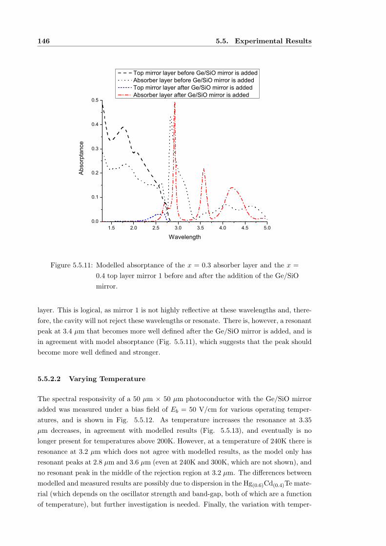
146 5.5. Experimental Results
1.5 2.0 2.5 3.0 3.5 4.0 4.5 5.00.0
0.1
0.2
0.3
0.4
0.5
Abs
orptan
ce
Wavelength
Top mirror layer before Ge/SiO mirror is added Absorber layer before Ge/SiO mirror is added Top mirror layer after Ge/SiO mirror is added Absorber layer after Ge/SiO mirror is added
Figure 5.5.11: Modelled absorptance of the x = 0.3 absorber layer and the x =
0.4 top layer mirror 1 before and after the addition of the Ge/SiO
mirror.
layer. This is logical, as mirror 1 is not highly reflective at these wavelengths and, there-
fore, the cavity will not reject these wavelengths or resonate. There is, however, a resonant
peak at 3.4 µm that becomes more well defined after the Ge/SiO mirror is added, and is
in agreement with model absorptance (Fig. 5.5.11), which suggests that the peak should
become more well defined and stronger.
5.5.2.2 Varying Temperature
The spectral responsivity of a 50 µm × 50 µm photoconductor with the Ge/SiO mirror
added was measured under a bias field of Eb = 50 V/cm for various operating temper-
atures, and is shown in Fig. 5.5.12. As temperature increases the resonance at 3.35
µm decreases, in agreement with modelled results (Fig. 5.5.13), and eventually is no
longer present for temperatures above 200K. However, at a temperature of 240K there is
resonance at 3.2 µm which does not agree with modelled results, as the model only has
resonant peaks at 2.8 µm and 3.6 µm (even at 240K and 300K, which are not shown), and
no resonant peak in the middle of the rejection region at 3.2 µm. The differences between
modelled and measured results are possibly due to dispersion in the Hg(0.6)Cd(0.4)Te mate-
rial (which depends on the oscillator strength and band-gap, both of which are a function
of temperature), but further investigation is needed. Finally, the variation with temper-
CHAPTER 5. Realisation of Resonant-cavity-enhanced Detectors 147
ature of the responsivity peak at approximately 2.8 µm is not monotonically shifting to
shorter wavelengths, suggesting that the signal at 2.8 µm is due to resonant absorption
in the cavity by the Hg(0.7)Cd(0.3)Te absorber layer.
5.5.3 Noise Measurements - MCT-79
Noise measurements were performed using a HP 3665A dynamic spectrum anaylser, with
the sample and dewar enclosed in a Faraday cage as illustrated in Fig. 5.5.14. The
current source (for biasing the photoconductor) was situated external to the Faraday
cage, as it must be powered by the mains 240V/50Hz supply. The voltage amplifier
is battery operated, and can therefore be placed within the Faraday cage in order to
avoid introducing extra noise. Noise measurements were taken on a number of different
devices, and at different bias conditions and temperatures. The results were inconclusive,
however, since the current source that was connected to the mains power supply tended
to introduce extra noise. Furthermore, with the very short lifetime of sample MCT-79,
the expected noise levels were very low, and the noise from the current supply was found
to dominate the signal. Figure 5.5.15 shows a typical noise profile measured from a 80
µm × 500 µm photoconductor at a temperature of 200K with bias fields of 0 V/cm and
22.5 V/cm. As expected, increasing the bias field increases the noise and, in particular,
the 1/f component: however, under bias the 1/f component deviates significantly from a
slope of -1, which is an indication that the current source used to bias the photoconductor
is affecting the measurement, as power spectral density of low frequency noise is typically
of the form
S(f) ∝ 1
fa(5.5.3)
where 0 < a < 2, and is typically close to 1 for electronic devices. As can be seen from Fig.
5.5.15, the 1/f noise component at high bias has a slope of -3, which is much greater than
explainable as noise from a simple photoconductor. One possible way to circumvent the
excess noise from the current source would be to use a battery bias voltage and suitably
large resistor to bias the photoconductor.
Nevertheless, the detector noise at the chopping frequency (150 Hz) has been extracted,
and used to calculate the detectivity of the RCE photoconductors. Peak detectivity at
80K for an 80 µm × 500 µm photoconductor was calculated to be 3.09×109 cm Hz1/2
W−1, while peak detectivity at 200K was calculated to be 4.48×108 cm Hz1/2 W−1. These
values represent a worst-case detectivity, as the devices would usually be operated beyond
the 1/f knee (thus reducing noise, and increasing detectivity), and also operated without
a noisy current supply. The measured detectivity is compared with D∗BLIP = 4×10¹¹
cm Hz1/2 W−1, which illustrates that this device is performing well below background
limited performance.
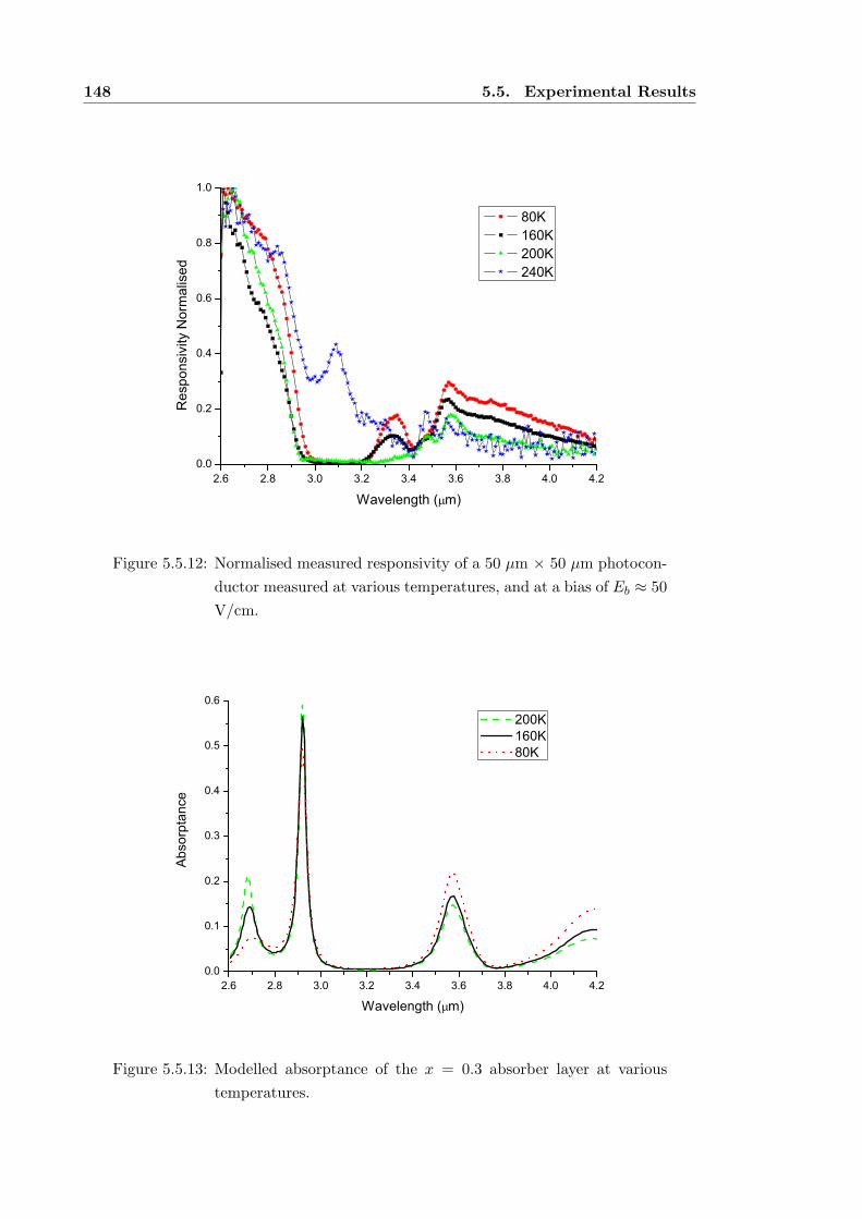
148 5.5. Experimental Results
2.6 2.8 3.0 3.2 3.4 3.6 3.8 4.0 4.20.0
0.2
0.4
0.6
0.8
1.0R
espo
nsiv
ity N
orm
alis
ed
Wavelength ( m)
80K 160K 200K 240K
Figure 5.5.12: Normalised measured responsivity of a 50 µm × 50 µm photocon-
ductor measured at various temperatures, and at a bias of Eb ≈ 50
V/cm.
2.6 2.8 3.0 3.2 3.4 3.6 3.8 4.0 4.20.0
0.1
0.2
0.3
0.4
0.5
0.6
Abs
orptan
ce
Wavelength ( m)
200K 160K 80K
Figure 5.5.13: Modelled absorptance of the x = 0.3 absorber layer at various
temperatures.
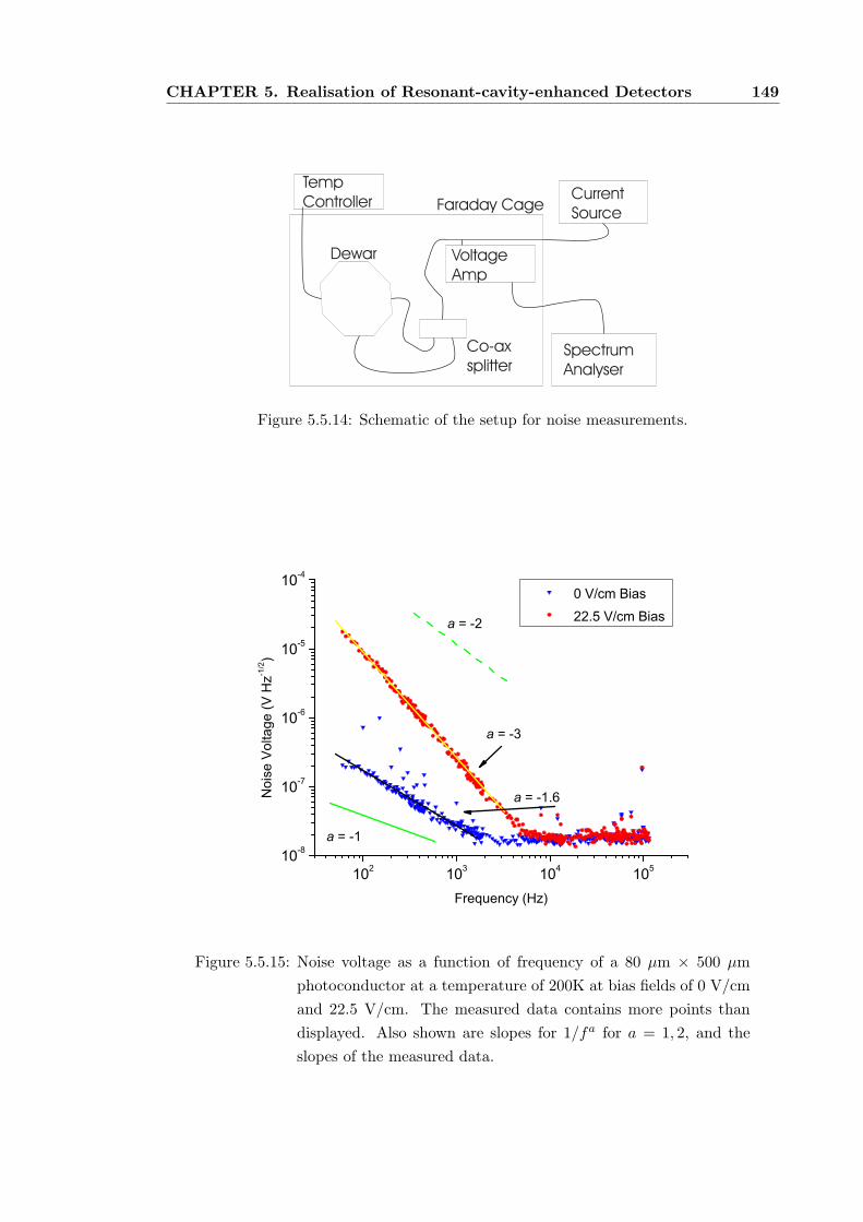
CHAPTER 5. Realisation of Resonant-cavity-enhanced Detectors 149
CurrentSource
VoltageAmp
Faraday Cage
Co-axsplitter
SpectrumAnalyser
Dewar
TempController
Figure 5.5.14: Schematic of the setup for noise measurements.
102 103 104 10510-8
10-7
10-6
10-5
10-4
a = -1.6
a = -2
a = -3
0 V/cm Bias 22.5 V/cm Bias
Noi
se V
olta
ge (V
Hz-1
/2)
Frequency (Hz)
a = -1
Figure 5.5.15: Noise voltage as a function of frequency of a 80 µm × 500 µm
photoconductor at a temperature of 200K at bias fields of 0 V/cm
and 22.5 V/cm. The measured data contains more points than
displayed. Also shown are slopes for 1/fa for a = 1, 2, and the
slopes of the measured data.
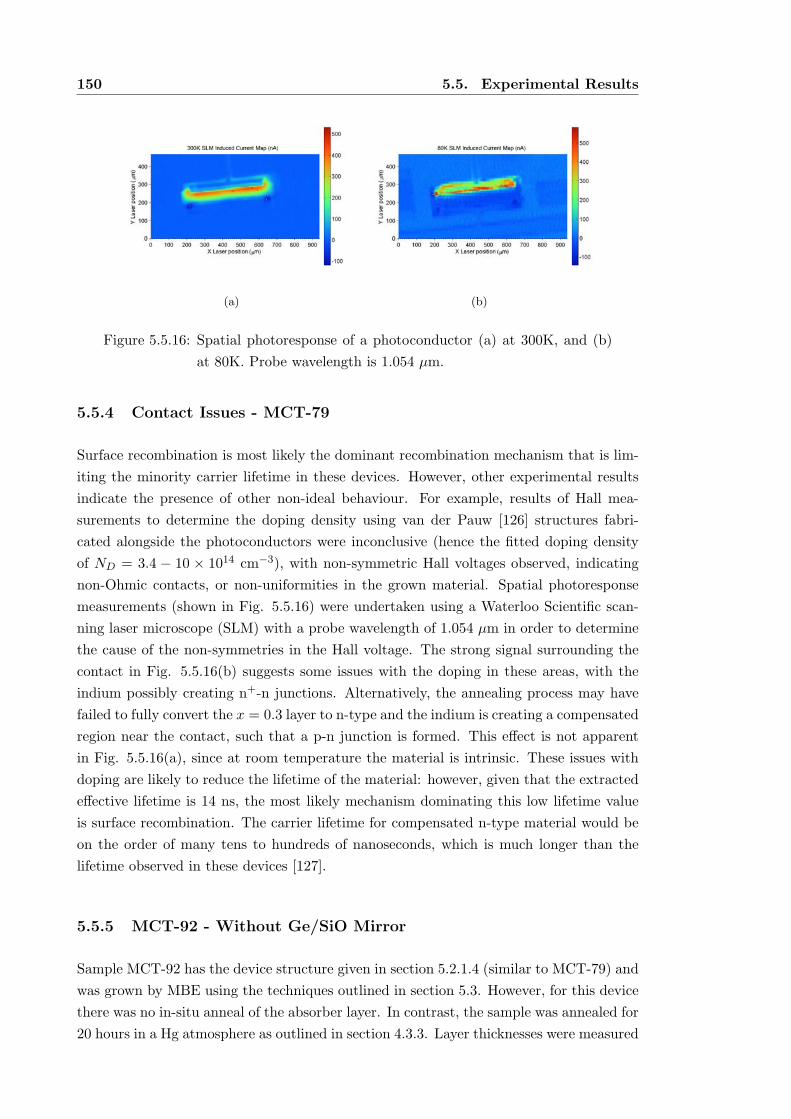
150 5.5. Experimental Results
(a) (b)
Figure 5.5.16: Spatial photoresponse of a photoconductor (a) at 300K, and (b)
at 80K. Probe wavelength is 1.054 µm.
5.5.4 Contact Issues - MCT-79
Surface recombination is most likely the dominant recombination mechanism that is lim-
iting the minority carrier lifetime in these devices. However, other experimental results
indicate the presence of other non-ideal behaviour. For example, results of Hall mea-
surements to determine the doping density using van der Pauw [126] structures fabri-
cated alongside the photoconductors were inconclusive (hence the fitted doping density
of ND = 3.4 − 10 × 1014 cm−3), with non-symmetric Hall voltages observed, indicating
non-Ohmic contacts, or non-uniformities in the grown material. Spatial photoresponse
measurements (shown in Fig. 5.5.16) were undertaken using a Waterloo Scientific scan-
ning laser microscope (SLM) with a probe wavelength of 1.054 µm in order to determine
the cause of the non-symmetries in the Hall voltage. The strong signal surrounding the
contact in Fig. 5.5.16(b) suggests some issues with the doping in these areas, with the
indium possibly creating n+-n junctions. Alternatively, the annealing process may have
failed to fully convert the x = 0.3 layer to n-type and the indium is creating a compensated
region near the contact, such that a p-n junction is formed. This effect is not apparent
in Fig. 5.5.16(a), since at room temperature the material is intrinsic. These issues with
doping are likely to reduce the lifetime of the material: however, given that the extracted
effective lifetime is 14 ns, the most likely mechanism dominating this low lifetime value
is surface recombination. The carrier lifetime for compensated n-type material would be
on the order of many tens to hundreds of nanoseconds, which is much longer than the
lifetime observed in these devices [127].
5.5.5 MCT-92 - Without Ge/SiO Mirror
Sample MCT-92 has the device structure given in section 5.2.1.4 (similar to MCT-79) and
was grown by MBE using the techniques outlined in section 5.3. However, for this device
there was no in-situ anneal of the absorber layer. In contrast, the sample was annealed for
20 hours in a Hg atmosphere as outlined in section 4.3.3. Layer thicknesses were measured
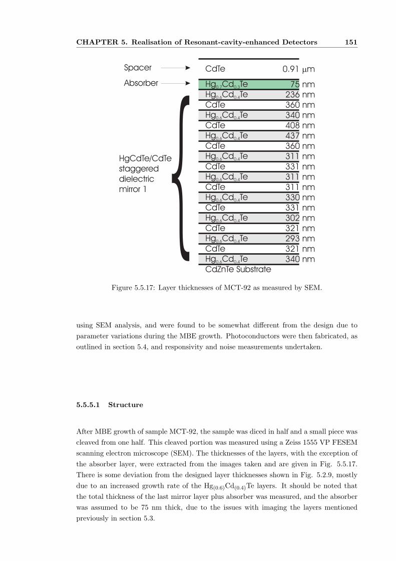
CHAPTER 5. Realisation of Resonant-cavity-enhanced Detectors 151
340 nm321 nm293 nm321 nm302 nm331 nm330 nm311 nm311 nm331 nm311 nm360 nm437 nm408 nm340 nm360 nm236 nm
Hg Cd Te0.6 0.4
CdTeHg Cd Te0.6 0.4
Hg Cd Te0.6 0.4
Hg Cd Te0.6 0.4
Hg Cd Te0.6 0.4
Hg Cd Te0.6 0.4
Hg Cd Te0.6 0.4
Hg Cd Te0.6 0.4
Hg Cd Te0.6 0.4
CdTe
CdTe
CdTe
CdTe
CdTe
CdTe
CdTe
CdZnTe Substrate
75 nmHg Cd Te0.7 0.3
0.91 mmCdTe
HgCdTe/CdTestaggereddielectricmirror 1
Spacer
Absorber
Figure 5.5.17: Layer thicknesses of MCT-92 as measured by SEM.
using SEM analysis, and were found to be somewhat different from the design due to
parameter variations during the MBE growth. Photoconductors were then fabricated, as
outlined in section 5.4, and responsivity and noise measurements undertaken.
5.5.5.1 Structure
After MBE growth of sample MCT-92, the sample was diced in half and a small piece was
cleaved from one half. This cleaved portion was measured using a Zeiss 1555 VP FESEM
scanning electron microscope (SEM). The thicknesses of the layers, with the exception of
the absorber layer, were extracted from the images taken and are given in Fig. 5.5.17.
There is some deviation from the designed layer thicknesses shown in Fig. 5.2.9, mostly
due to an increased growth rate of the Hg(0.6)Cd(0.4)Te layers. It should be noted that
the total thickness of the last mirror layer plus absorber was measured, and the absorber
was assumed to be 75 nm thick, due to the issues with imaging the layers mentioned
previously in section 5.3.
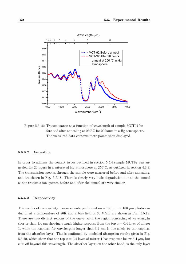
152 5.5. Experimental Results
1000 1500 2000 2500 3000 3500 40000.0
0.1
0.2
0.3
0.4
0.5
0.6
0.7
0.8
0.9
1.010 9 8 7 6 5 4 3
Tran
smittan
ce
Wavenumber (cm-1)
MCT-92 Before anneal MCT-92 After 20 hours
anneal at 250 oC in Hgatmosphere
Wavelength ( m)
Figure 5.5.18: Transmittance as a function of wavelength of sample MCT92 be-
fore and after annealing at 250C for 20 hours in a Hg atmosphere.
The measured data contains more points than displayed.
5.5.5.2 Annealing
In order to address the contact issues outlined in section 5.5.4 sample MCT92 was an-
nealed for 20 hours in a saturated Hg atmosphere at 250C, as outlined in section 4.3.3.
The transmission spectra through the sample were measured before and after annealing,
and are shown in Fig. 5.5.18. There is clearly very little degradation due to the anneal
as the transmission spectra before and after the anneal are very similar.
5.5.5.3 Responsivity
The results of responsivity measurements performed on a 100 µm × 100 µm photocon-
ductor at a temperature of 80K and a bias field of 36 V/cm are shown in Fig. 5.5.19.
There are two distinct regions of the curve, with the region consisting of wavelengths
shorter than 3.4 µm showing a much higher response from the top x = 0.4 layer of mirror
1, while the response for wavelengths longer than 3.4 µm is due solely to the response
from the absorber layer. This is confirmed by modelled absorption results given in Fig.
5.5.20, which show that the top x = 0.4 layer of mirror 1 has response below 3.4 µm, but
cuts off beyond this wavelength. The absorber layer, on the other hand, is the only layer
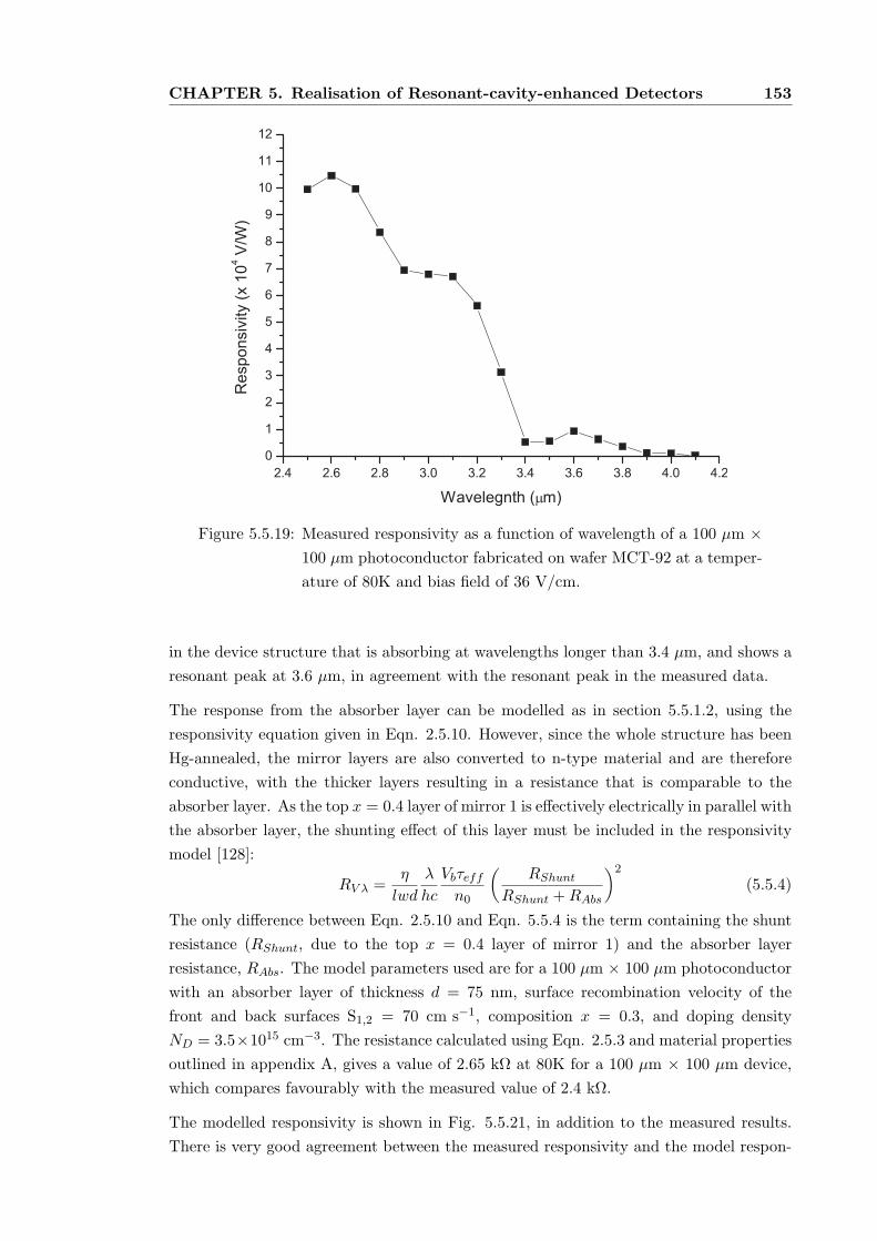
CHAPTER 5. Realisation of Resonant-cavity-enhanced Detectors 153
Figure 5.5.19: Measured responsivity as a function of wavelength of a 100 µm ×100 µm photoconductor fabricated on wafer MCT-92 at a temper-
ature of 80K and bias field of 36 V/cm.
in the device structure that is absorbing at wavelengths longer than 3.4 µm, and shows a
resonant peak at 3.6 µm, in agreement with the resonant peak in the measured data.
The response from the absorber layer can be modelled as in section 5.5.1.2, using the
responsivity equation given in Eqn. 2.5.10. However, since the whole structure has been
Hg-annealed, the mirror layers are also converted to n-type material and are therefore
conductive, with the thicker layers resulting in a resistance that is comparable to the
absorber layer. As the top x = 0.4 layer of mirror 1 is effectively electrically in parallel with
the absorber layer, the shunting effect of this layer must be included in the responsivity
model [128]:
RV λ =η
lwd
λ
hc
Vbτeff
n0
(
RShunt
RShunt +RAbs
)2
(5.5.4)
The only difference between Eqn. 2.5.10 and Eqn. 5.5.4 is the term containing the shunt
resistance (RShunt, due to the top x = 0.4 layer of mirror 1) and the absorber layer
resistance, RAbs. The model parameters used are for a 100 µm × 100 µm photoconductor
with an absorber layer of thickness d = 75 nm, surface recombination velocity of the
front and back surfaces S1,2 = 70 cm s−1, composition x = 0.3, and doping density
ND = 3.5×1015 cm−3. The resistance calculated using Eqn. 2.5.3 and material properties
outlined in appendix A, gives a value of 2.65 kΩ at 80K for a 100 µm × 100 µm device,
which compares favourably with the measured value of 2.4 kΩ.
The modelled responsivity is shown in Fig. 5.5.21, in addition to the measured results.
There is very good agreement between the measured responsivity and the model respon-
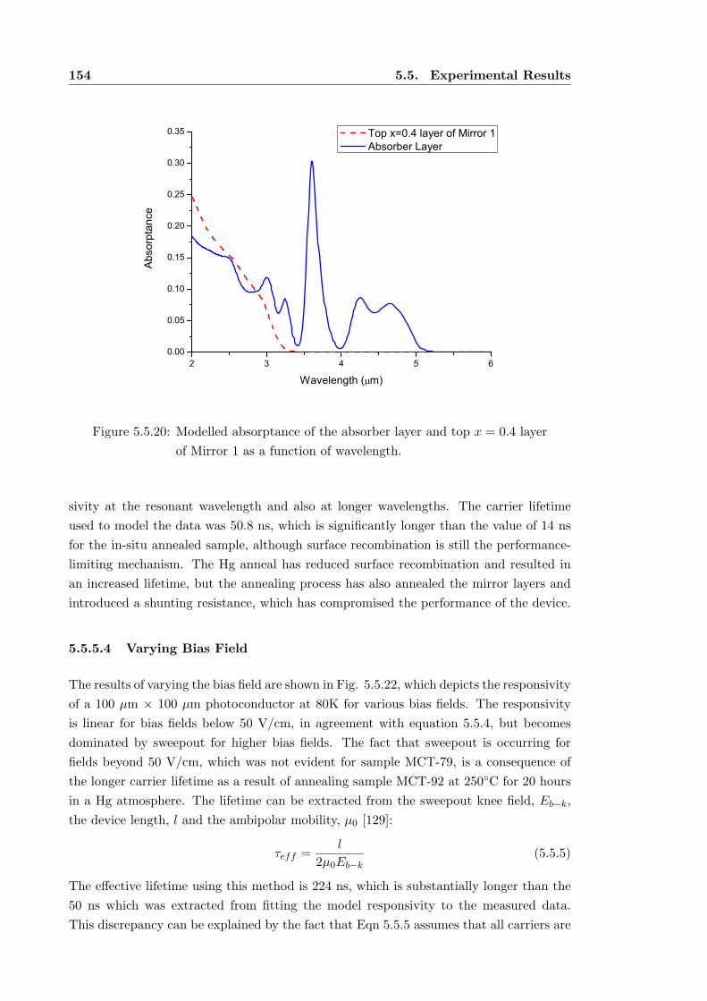
154 5.5. Experimental Results
2 3 4 5 60.00
0.05
0.10
0.15
0.20
0.25
0.30
0.35
Abs
orptan
ce
Wavelength ( m)
Top x=0.4 layer of Mirror 1 Absorber Layer
Figure 5.5.20: Modelled absorptance of the absorber layer and top x = 0.4 layer
of Mirror 1 as a function of wavelength.
sivity at the resonant wavelength and also at longer wavelengths. The carrier lifetime
used to model the data was 50.8 ns, which is significantly longer than the value of 14 ns
for the in-situ annealed sample, although surface recombination is still the performance-
limiting mechanism. The Hg anneal has reduced surface recombination and resulted in
an increased lifetime, but the annealing process has also annealed the mirror layers and
introduced a shunting resistance, which has compromised the performance of the device.
5.5.5.4 Varying Bias Field
The results of varying the bias field are shown in Fig. 5.5.22, which depicts the responsivity
of a 100 µm × 100 µm photoconductor at 80K for various bias fields. The responsivity
is linear for bias fields below 50 V/cm, in agreement with equation 5.5.4, but becomes
dominated by sweepout for higher bias fields. The fact that sweepout is occurring for
fields beyond 50 V/cm, which was not evident for sample MCT-79, is a consequence of
the longer carrier lifetime as a result of annealing sample MCT-92 at 250C for 20 hours
in a Hg atmosphere. The lifetime can be extracted from the sweepout knee field, Eb−k,
the device length, l and the ambipolar mobility, µ0 [129]:
τeff =l
2µ0Eb−k(5.5.5)
The effective lifetime using this method is 224 ns, which is substantially longer than the
50 ns which was extracted from fitting the model responsivity to the measured data.
This discrepancy can be explained by the fact that Eqn 5.5.5 assumes that all carriers are
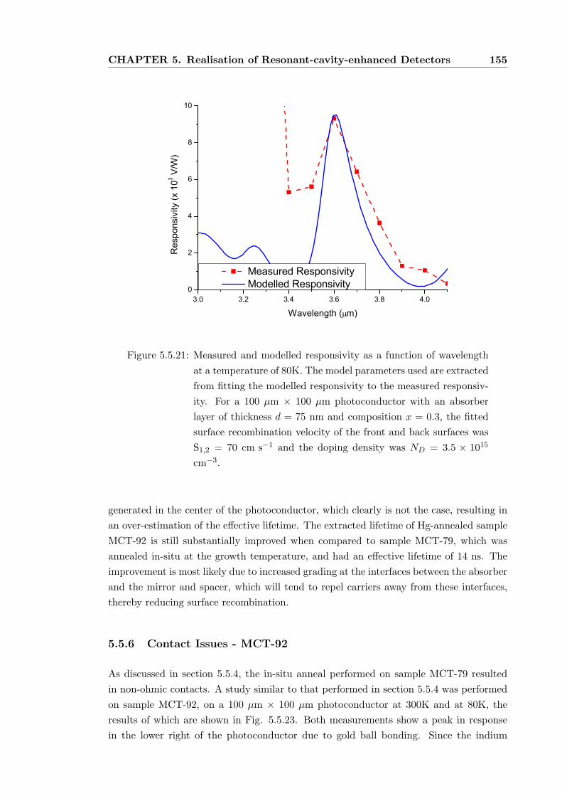
CHAPTER 5. Realisation of Resonant-cavity-enhanced Detectors 155
3.0 3.2 3.4 3.6 3.8 4.00
2
4
6
8
10
Res
pons
ivity
(x 1
03 V/W
)
Wavelength ( m)
Measured Responsivity Modelled Responsivity
Figure 5.5.21: Measured and modelled responsivity as a function of wavelength
at a temperature of 80K. The model parameters used are extracted
from fitting the modelled responsivity to the measured responsiv-
ity. For a 100 µm × 100 µm photoconductor with an absorber
layer of thickness d = 75 nm and composition x = 0.3, the fitted
surface recombination velocity of the front and back surfaces was
S1,2 = 70 cm s−1 and the doping density was ND = 3.5 × 10¹⁵
cm−3.
generated in the center of the photoconductor, which clearly is not the case, resulting in
an over-estimation of the effective lifetime. The extracted lifetime of Hg-annealed sample
MCT-92 is still substantially improved when compared to sample MCT-79, which was
annealed in-situ at the growth temperature, and had an effective lifetime of 14 ns. The
improvement is most likely due to increased grading at the interfaces between the absorber
and the mirror and spacer, which will tend to repel carriers away from these interfaces,
thereby reducing surface recombination.
5.5.6 Contact Issues - MCT-92
As discussed in section 5.5.4, the in-situ anneal performed on sample MCT-79 resulted
in non-ohmic contacts. A study similar to that performed in section 5.5.4 was performed
on sample MCT-92, on a 100 µm × 100 µm photoconductor at 300K and at 80K, the
results of which are shown in Fig. 5.5.23. Both measurements show a peak in response
in the lower right of the photoconductor due to gold ball bonding. Since the indium
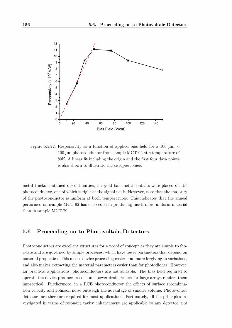
156 5.6. Proceeding on to Photovoltaic Detectors
0 20 40 60 80 100 120 1400
1
2
3
4
5
6
7
8
9
10
11
12
Res
pons
ivity
(x 1
03 V/W
)
Bias Field (V/cm)
Figure 5.5.22: Responsivity as a function of applied bias field for a 100 µm ×100 µm photoconductor from sample MCT-92 at a temperature of
80K. A linear fit including the origin and the first four data points
is also shown to illustrate the sweepout knee.
metal tracks contained discontinuities, the gold ball metal contacts were placed on the
photoconductor, one of which is right at the signal peak. However, note that the majority
of the photoconductor is uniform at both temperatures. This indicates that the anneal
performed on sample MCT-92 has succeeded in producing much more uniform material
than in sample MCT-79.
5.6 Proceeding on to Photovoltaic Detectors
Photoconductors are excellent structures for a proof of concept as they are simple to fab-
ricate and are governed by simple processes, which have fewer parameters that depend on
material properties. This makes device processing easier, and more forgiving to variations,
and also makes extracting the material parameters easier than for photodiodes. However,
for practical applications, photoconductors are not suitable. The bias field required to
operate the device produces a constant power drain, which for large arrays renders them
impractical. Furthermore, in a RCE photoconductor the effects of surface recombina-
tion velocity and Johnson noise outweigh the advantage of smaller volume. Photovoltaic
detectors are therefore required for most applications. Fortunately, all the principles in-
vestigated in terms of resonant cavity enhancement are applicable to any detector, not
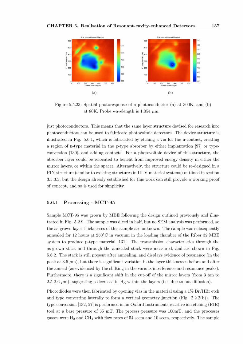
CHAPTER 5. Realisation of Resonant-cavity-enhanced Detectors 157
(a) (b)
Figure 5.5.23: Spatial photoresponse of a photoconductor (a) at 300K, and (b)
at 80K. Probe wavelength is 1.054 µm.
just photoconductors. This means that the same layer structure devised for research into
photoconductors can be used to fabricate photovoltaic detectors. The device structure is
illustrated in Fig. 5.6.1, which is fabricated by etching a via for the n-contact, creating
a region of n-type material in the p-type absorber by either implantation [97] or type-
conversion [130], and adding contacts. For a photovoltaic device of this structure, the
absorber layer could be relocated to benefit from improved energy density in either the
mirror layers, or within the spacer. Alternatively, the structure could be re-designed in a
PIN structure (similar to existing structures in III-V material systems) outlined in section
3.5.3.3, but the design already established for this work can still provide a working proof
of concept, and so is used for simplicity.
5.6.1 Processing - MCT-95
Sample MCT-95 was grown by MBE following the design outlined previously and illus-
trated in Fig. 5.2.9. The sample was diced in half, but no SEM analysis was performed, so
the as-grown layer thicknesses of this sample are unknown. The sample was subsequently
annealed for 12 hours at 250C in vacuum in the loading chamber of the Riber 32 MBE
system to produce p-type material [131]. The transmission characteristics through the
as-grown stack and through the annealed stack were measured, and are shown in Fig.
5.6.2. The stack is still present after annealing, and displays evidence of resonance (in the
peak at 3.5 µm), but there is significant variation in the layer thicknesses before and after
the anneal (as evidenced by the shifting in the various interference and resonance peaks).
Furthermore, there is a significant shift in the cut-off of the mirror layers (from 3 µm to
2.5-2.6 µm), suggesting a decrease in Hg within the layers (i.e. due to out-diffusion).
Photodiodes were then fabricated by opening vias in the material using a 1% Br/HBr etch
and type converting laterally to form a vertical geometry junction (Fig. 2.2.2(b)). The
type conversion [132, 57] is performed in an Oxford Instruments reactive ion etching (RIE)
tool at a base pressure of 35 mT. The process pressure was 100mT, and the processes
gasses were H2 and CH4 with flow rates of 54 sccm and 10 sccm, respectively. The sample
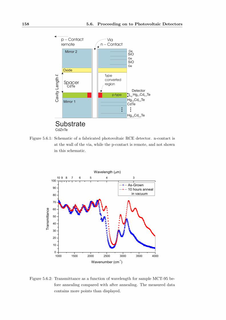
158 5.6. Proceeding on to Photovoltaic Detectors
Cavity L
ength
l
SubstrateCdZnTe
Mirror 1
SpacerCdTe
Ld
CdTe
Hg Cd Te0.6 0.4
Hg Cd Te0.6 0.4
Mirror 2SiOGe
SiOGe
Ge
Oxide
Vian – Contact
Typeconvertedregion
p-type
DetectorHg Cd Te0.7 0.3
p – Contactremote
Figure 5.6.1: Schematic of a fabricated photovoltaic RCE detector. n-contact is
at the wall of the via, while the p-contact is remote, and not shown
in this schematic.
1000 1500 2000 2500 3000 3500 40000
10
20
30
40
50
60
70
80
90
10010 9 8 7 6 5 4 3
Tran
smittan
ce
Wavenumber (cm-1)
As-Grown 10 hours anneal
in vacuum
Wavelength ( m)
Figure 5.6.2: Transmittance as a function of wavelength for sample MCT-95 be-
fore annealing compared with after annealing. The measured data
contains more points than displayed.
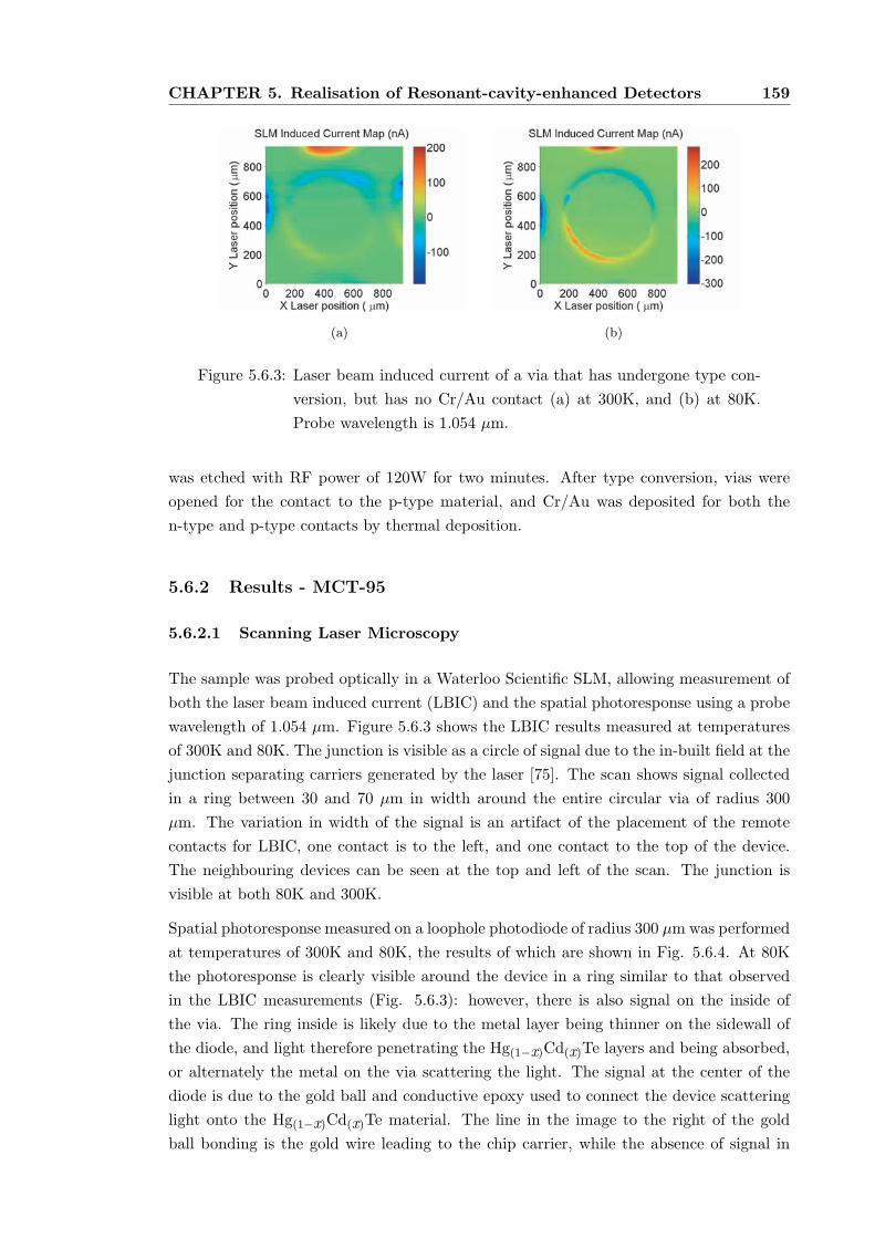
CHAPTER 5. Realisation of Resonant-cavity-enhanced Detectors 159
(a) (b)
Figure 5.6.3: Laser beam induced current of a via that has undergone type con-
version, but has no Cr/Au contact (a) at 300K, and (b) at 80K.
Probe wavelength is 1.054 µm.
was etched with RF power of 120W for two minutes. After type conversion, vias were
opened for the contact to the p-type material, and Cr/Au was deposited for both the
n-type and p-type contacts by thermal deposition.
5.6.2 Results - MCT-95
5.6.2.1 Scanning Laser Microscopy
The sample was probed optically in a Waterloo Scientific SLM, allowing measurement of
both the laser beam induced current (LBIC) and the spatial photoresponse using a probe
wavelength of 1.054 µm. Figure 5.6.3 shows the LBIC results measured at temperatures
of 300K and 80K. The junction is visible as a circle of signal due to the in-built field at the
junction separating carriers generated by the laser [75]. The scan shows signal collected
in a ring between 30 and 70 µm in width around the entire circular via of radius 300
µm. The variation in width of the signal is an artifact of the placement of the remote
contacts for LBIC, one contact is to the left, and one contact to the top of the device.
The neighbouring devices can be seen at the top and left of the scan. The junction is
visible at both 80K and 300K.
Spatial photoresponse measured on a loophole photodiode of radius 300 µm was performed
at temperatures of 300K and 80K, the results of which are shown in Fig. 5.6.4. At 80K
the photoresponse is clearly visible around the device in a ring similar to that observed
in the LBIC measurements (Fig. 5.6.3): however, there is also signal on the inside of
the via. The ring inside is likely due to the metal layer being thinner on the sidewall of
the diode, and light therefore penetrating the Hg(1−x)Cd(x)Te layers and being absorbed,
or alternately the metal on the via scattering the light. The signal at the center of the
diode is due to the gold ball and conductive epoxy used to connect the device scattering
light onto the Hg(1−x)Cd(x)Te material. The line in the image to the right of the gold
ball bonding is the gold wire leading to the chip carrier, while the absence of signal in
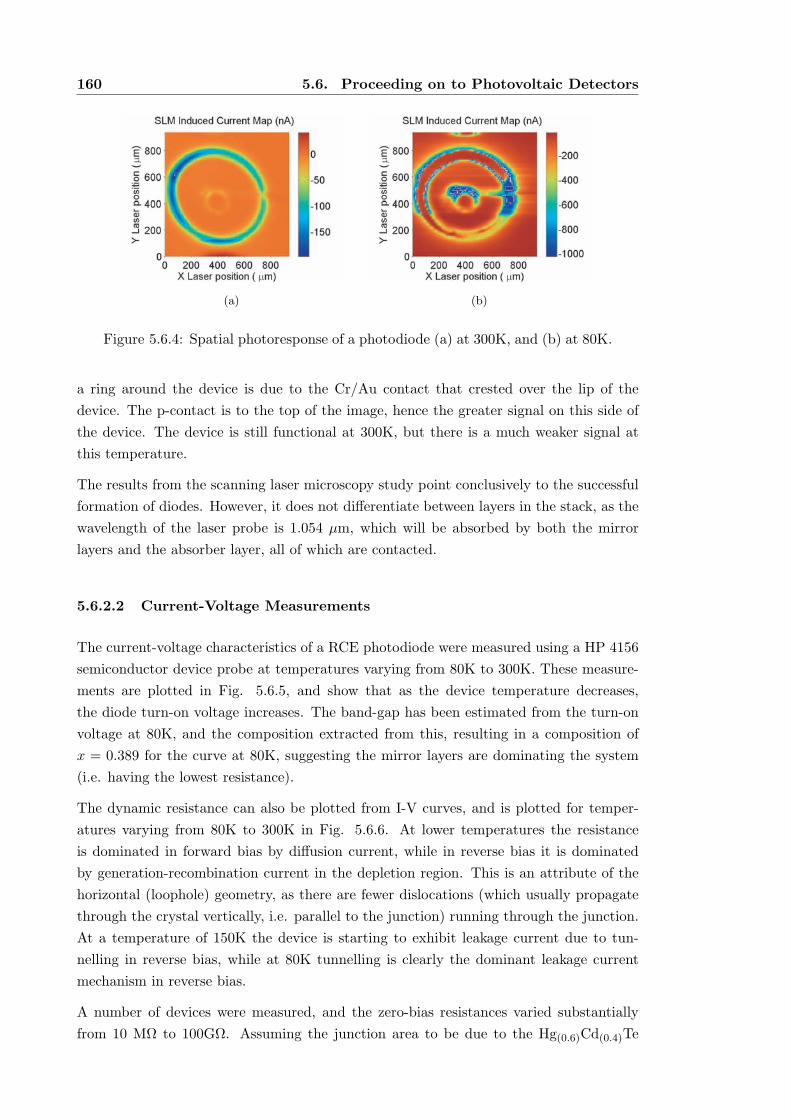
160 5.6. Proceeding on to Photovoltaic Detectors
(a) (b)
Figure 5.6.4: Spatial photoresponse of a photodiode (a) at 300K, and (b) at 80K.
a ring around the device is due to the Cr/Au contact that crested over the lip of the
device. The p-contact is to the top of the image, hence the greater signal on this side of
the device. The device is still functional at 300K, but there is a much weaker signal at
this temperature.
The results from the scanning laser microscopy study point conclusively to the successful
formation of diodes. However, it does not differentiate between layers in the stack, as the
wavelength of the laser probe is 1.054 µm, which will be absorbed by both the mirror
layers and the absorber layer, all of which are contacted.
5.6.2.2 Current-Voltage Measurements
The current-voltage characteristics of a RCE photodiode were measured using a HP 4156
semiconductor device probe at temperatures varying from 80K to 300K. These measure-
ments are plotted in Fig. 5.6.5, and show that as the device temperature decreases,
the diode turn-on voltage increases. The band-gap has been estimated from the turn-on
voltage at 80K, and the composition extracted from this, resulting in a composition of
x = 0.389 for the curve at 80K, suggesting the mirror layers are dominating the system
(i.e. having the lowest resistance).
The dynamic resistance can also be plotted from I-V curves, and is plotted for temper-
atures varying from 80K to 300K in Fig. 5.6.6. At lower temperatures the resistance
is dominated in forward bias by diffusion current, while in reverse bias it is dominated
by generation-recombination current in the depletion region. This is an attribute of the
horizontal (loophole) geometry, as there are fewer dislocations (which usually propagate
through the crystal vertically, i.e. parallel to the junction) running through the junction.
At a temperature of 150K the device is starting to exhibit leakage current due to tun-
nelling in reverse bias, while at 80K tunnelling is clearly the dominant leakage current
mechanism in reverse bias.
A number of devices were measured, and the zero-bias resistances varied substantially
from 10 MΩ to 100GΩ. Assuming the junction area to be due to the Hg(0.6)Cd(0.4)Te
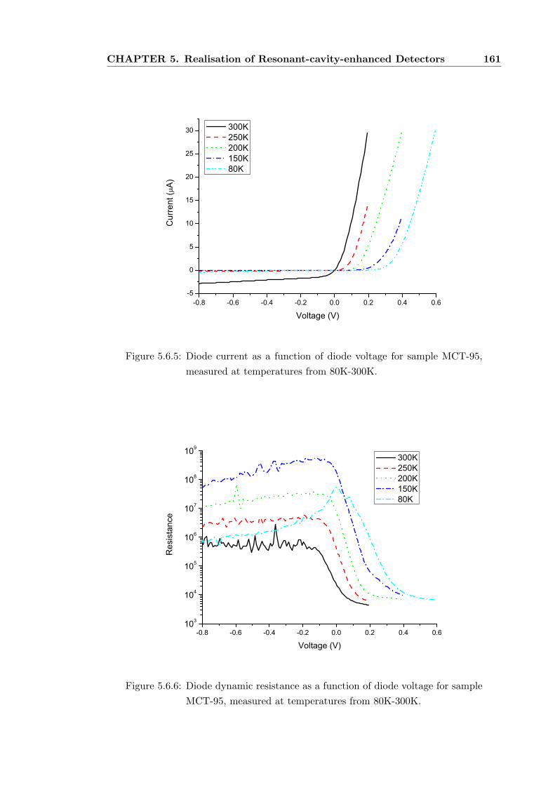
CHAPTER 5. Realisation of Resonant-cavity-enhanced Detectors 161
-0.8 -0.6 -0.4 -0.2 0.0 0.2 0.4 0.6-5
0
5
10
15
20
25
30
Cur
rent
(A
)
Voltage (V)
300K 250K 200K 150K 80K
Figure 5.6.5: Diode current as a function of diode voltage for sample MCT-95,
measured at temperatures from 80K-300K.
-0.8 -0.6 -0.4 -0.2 0.0 0.2 0.4 0.6103
104
105
106
107
108
109
Res
istanc
e
Voltage (V)
300K 250K 200K 150K 80K
Figure 5.6.6: Diode dynamic resistance as a function of diode voltage for sample
MCT-95, measured at temperatures from 80K-300K.
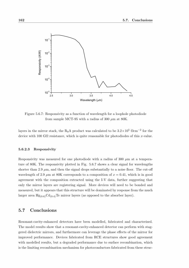
162 5.7. Conclusions
2.5 3.0 3.5 4.0 4.510-5
10-4
10-3
10-2
10-1R
espo
nsiv
ity (A
/W)
Wavelength ( m)
Figure 5.6.7: Responsivity as a function of wavelength for a loophole photodiode
from sample MCT-95 with a radius of 300 µm at 80K.
layers in the mirror stack, the R0A product was calculated to be 3.2×10⁵ Ωcm−2 for the
device with 100 GΩ resistance, which is quite reasonable for photodiodes of this x-value.
5.6.2.3 Responsivity
Responsivity was measured for one photodiode with a radius of 300 µm at a tempera-
ture of 80K. The responsivity plotted in Fig. 5.6.7 shows a clear signal for wavelengths
shorter than 2.9 µm, and then the signal drops substantially to a noise floor. The cut-off
wavelength of 2.9 µm at 80K corresponds to a composition of x = 0.41, which is in good
agreement with the composition extracted using the I-V data, further suggesting that
only the mirror layers are registering signal. More devices will need to be bonded and
measured, but it appears that this structure will be dominated by response from the much
larger area Hg(0.6)Cd(0.4)Te mirror layers (as opposed to the absorber layer).
5.7 Conclusions
Resonant-cavity-enhanced detectors have been modelled, fabricated and characterised.
The model results show that a resonant-cavity-enhanced detector can perform with stag-
gered dielectric mirrors, and furthermore can leverage the phase effects of the mirror for
improved performance. Devices fabricated from RCE structures show good agreement
with modelled results, but a degraded performance due to surface recombination, which
is the limiting recombination mechanism for photoconductors fabricated from these struc-
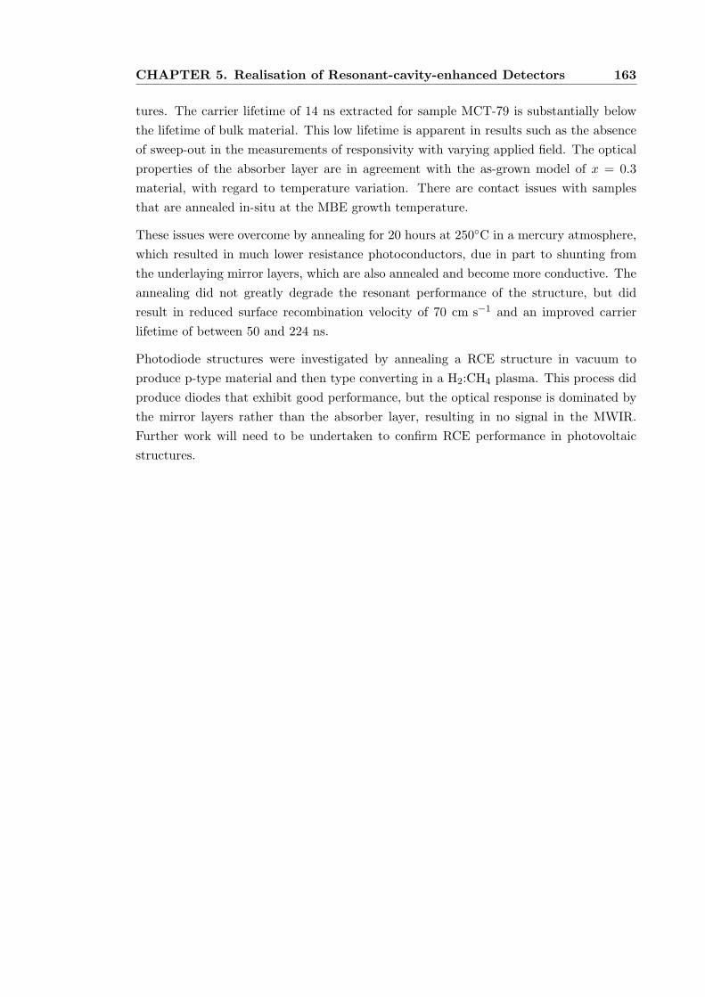
CHAPTER 5. Realisation of Resonant-cavity-enhanced Detectors 163
tures. The carrier lifetime of 14 ns extracted for sample MCT-79 is substantially below
the lifetime of bulk material. This low lifetime is apparent in results such as the absence
of sweep-out in the measurements of responsivity with varying applied field. The optical
properties of the absorber layer are in agreement with the as-grown model of x = 0.3
material, with regard to temperature variation. There are contact issues with samples
that are annealed in-situ at the MBE growth temperature.
These issues were overcome by annealing for 20 hours at 250C in a mercury atmosphere,
which resulted in much lower resistance photoconductors, due in part to shunting from
the underlaying mirror layers, which are also annealed and become more conductive. The
annealing did not greatly degrade the resonant performance of the structure, but did
result in reduced surface recombination velocity of 70 cm s−1 and an improved carrier
lifetime of between 50 and 224 ns.
Photodiode structures were investigated by annealing a RCE structure in vacuum to
produce p-type material and then type converting in a H2:CH4 plasma. This process did
produce diodes that exhibit good performance, but the optical response is dominated by
the mirror layers rather than the absorber layer, resulting in no signal in the MWIR.
Further work will need to be undertaken to confirm RCE performance in photovoltaic
structures.

164 5.7. Conclusions
Chapter 6Summary and Conclusions
6.1 Thesis Objectives
The principle objectives of this work were to investigate resonant-cavity-enhanced (RCE)
detectors, and to prove the concept of resonant-cavity-enhancement for IR detectors by
undertaking the following:
• Investigate the design and modelling of RCE devices and determine a structure to
prove the concept of RCE using the Hg(1−x)Cd(x)Te material system.
• Fabricate mirror structures and RCE detector structures, and characterise optical
performance.
• Fabricate devices from the RCE detector structure and characterise device perfor-
mance, showing that resonant-cavity-enhanced performance is possible for HgCdTe
based IR detectors.
6.2 Outcomes
The specific outcomes of this thesis are:
1. Design and modelling:
• The benefits of resonant-cavity-enhanced detectors have been modelled in terms
of increasing operating temperature and reducing the noise due to thermal gen-
eration and recombination of carriers in RCE devices.
• The Hg(1−x)Cd(x)Te material system has been investigated as a suitable system
for growing RCE structures. MBE growth of Hg(1−x)Cd(x)Te was investigated
as the growth method.
166 6.2. Outcomes
• Staggered dielectric mirrors have been investigated as a means of improving the
mirror response of Hg(1−x)Cd(x)Te/CdTe mirrors. Staggered dielectric mirrors
allow for a broader region of high reflectivity, at the expense of reducing re-
flectivity, for a given number of layers. This is useful for material systems such
as Hg(1−x)Cd(x)Te/CdTe, where the ratio of refractive indices is close to unity,
suggesting a narrow region of high reflectivity for a quarter-wave stack design.
• RCE structures were investigated and a proof-of-concept design balancing im-
proved performance, wide spectral range, absorber layer thickness and position,
target device, and growth times was derived.
• RCE performance was modelled for the Hg(1−x)Cd(x)Te material system, illus-
trating the improved performance.
2. Mirrors:
• Alternating layers of Hg(1−x)Cd(x)Te and CdTe have been grown by MBE at
a constant temperature to create mirror layers, showing that CdTe can be
grown on layers of Hg(1−x)Cd(x)Te, while maintaining a crystal structure that
supports growth of further mirror layers (without decreasing mercury content)
and absorber layers.
• Mirror performance has been characterised by FTIR transmission measure-
ments, showing good agreement with model results, except for a discrepancy
with the refractive index of CdTe in the mirror layers.
• Ellipsometry measurements indicate a discrepancy between the refractive index
model of crystalline CdTe and the as-grown CdTe in the mirror layers.
• Annealing is a critical step in device fabrication and, therefore, annealing was
performed on mirror stacks to characterize performance after annealing. Mirror
stacks have been annealed for up to 20 hours at 250 degrees in a mercury
atmosphere. Transmission measurements and interdiffusion modelling indicate
that the mirror stack have survived annealing at these temperatures for these
time periods.
• Secondary ion mass spectroscopy measurements of annealed mirror structures
also show that the mirror structures survived the annealing without any major
structural modifications.
3. Experimental RCE Detectors:
• RCE structures were grown by MBE, and characterised by FTIR transmission
measurements. There is good agreement with modelled results, with resonance
peaks, reflection peaks and transmission peaks all appearing in the model.
• Photoconductors were fabricated from the MBE grown RCE structures and
were characterised by responsivity measurements, noise measurements, and
using I-V measurements.
CHAPTER 6. Summary and Conclusions 167
• Effective carrier lifetime has been extracted from responsivity measurements,
as well as surface recombination velocity and interface trap density. The ef-
fective carrier lifetime for samples annealed in-situ was extracted to be 14 ns,
while samples that were Hg-annealed ex-situ had effective lifetimes of 50-224
ns. These lifetimes corresponded to surface recombination velocities of 300
cm s−1 and 70 cm s−1, respectively.
• Electric contact issues were investigated using laser beam induced current and
scanning laser microscopy techniques. Issues with the contacts were revealed,
which indicated problems with the in-situ annealing techniques used.
• The RCE structures were annealed and showed improved contact performance.
• RCE photodiodes were fabricated by p-to-n type converting vacuum annealed
p-type structures in a H2:CH4 plasma. These structures exhibited good elec-
trical diode performance: however, it was not possible to extract an optical
signal due to shunting by the mirror layers.
6.3 Original Results
Original results generated by this thesis include:
• Models were developed and utilised to accurately predict optical characteristics as
well as device performance and detectivity. Models were also used to predict the
lower refractive index of the low growth temperature CdTe, and to extract the
refractive index of this as-grown CdTe.
• Modelling of Hg(1−x)Cd(x)Te/CdTe mirror stacks and RCE structures yielded a
design that balances improved performance, wide spectral range, absorber layer
thickness and position, target device, and growth times. The design used 17 layers
for a staggered dielectric mirror with a small common ratio of 1.017 and a starting
wavelength of 3 µm. An absorber layer of 75 nm thickness was used, which is grown
directly on the top layer of the staggered dielectric mirror (to provide a better
crystalline surface on-which to grow). The spacer layer was also grown in-situ in
order to decrease surface recombination, and CdTe was used as a spacer material
to reduce shunting of the photoconductors.
• Mirrors consisting of a 17 layer staggered Hg(1−x)Cd(x)Te/CdTe dielectric design
and fabricated by MBE exhibit good 2-D crystallinity in the Hg(1−x)Cd(x)Te lay-
ers, after an initial period of poor growth on CdTe. CdTe layers exhibit degraded
crystal quality as a result of being grown at the optimum growth temperature for
the Hg(1−x)Cd(x)Te layers, which is substantially lower than required for crystalline
CdTe. The refractive index of the as-grown CdTe is reduced, and an incorporation of
10 % voids accounts for the reduction in refractive index to 2.4-2.5 in the wavelength
range of interest. Mirror layers fabricated by MBE can survive 20 hours anneal-
ing at 250 degrees in a mercury atmosphere. There is a degradation in reflectivity
168 6.3. Original Results
associated with annealing the sample due to interdiffusion of mercury between the
layers, causing grading of the interface but this is not enough to degrade the mea-
sured reflectivity by more than a few percent. SIMS measurements performed on
annealed samples show that the interdiffusion at the CdTe on Hg(1−x)Cd(x)Te inter-
face is very close to reported literature results. Interdiffusion at the Hg(1−x)Cd(x)Te
on CdTe interface is greater than reported in the literature, probably due to an
increased defect density. Mirror layers exhibit a change in the refractive index of
the CdTe layers. This is due to the incorporation of voids in the CdTe layers during
growth, as ellipsometry measurements suggest a void density of around ten percent
in these layers.
• RCE photoconductors fabricated using a 17 layer staggered dielectric mirror, a 75
nm absorber layer and a spacer layer of approximately 1 µm have been fabricated
and characterised. The measured responsivity shows resonance and good agreement
with modelled results. Peak responsivity was measured as 8×10⁴ V/W for a 50
µm × 50 µm photoconductor at 200K, for a bias field of Eb = 36 Vcm−1. This
represents the first reported response from a RCE structure with a Hg(0.7)Cd(0.3)Te
absorber layer. For sample MCT-79 the surface recombination velocity is 300-600
cm s−1. This surface recombination, while satisfactory for thicker absorbing layers,
is substantial enough to significantly reduce the effective carrier lifetime in RCE
photoconductors as the absorber layer is so thin. The effective lifetime extracted
from the responsivity results is approximately 14ns. This is approximately 2 orders
of magnitude lower than the bulk lifetime for Hg(1−x)Cd(x)Te of similar composition
and doping density. Variable bias field measurements do not show evidence of sweep-
out, in accordance with the very low lifetime of the material.
• RCE photoconductors fabricated from material that was annealed for 20 hours in
a Hg atmosphere at 250C addressed the problems with the contacts of sample
MCT79. However, the anneal affected all layers of the structure, resulting in the
absorber layer being shunted by the Hg(0.6)Cd(0.4)Te layer on which the absorber
sits. The anneal did reduce the surface recombination velocity to between 50 and
70 cm s−1, which corresponds to an effective lifetime of 224 ns, and produced more
uniform material based on spatial photoresponse scans.
• RCE photodiodes have also been investigated. However, although the diodes ex-
hibited good electrical characteristics, they did not provide optical response in the
MWIR due to the mirror layers shunting the absorber.
CHAPTER 6. Summary and Conclusions 169
6.4 Conclusions
Resonant-cavity-enhancement is a technique that can be used to improve detector per-
formance by reducing noise due to thermally generated carriers, while maintaining high
quantum efficiency at the resonant wavelengths. This can be important for many types
of infrared detectors and has been investigated by fabricating RCE detectors using the
Hg(1−x)Cd(x)Te material system. The benefits of RCE detectors have been modelled, and
show improvement in detectivity, or allow higher operating temperature while maintaining
detectivity, due to the reduction of thermally generated carriers.
Mirrors required to facilitate the fabrication of RCE photoconductors using an absorber
layer of 75 nm thickness and Hg(0.7)Cd(0.3)Te material have been characterised and shown
to provide good mirror performance which agrees with modelled results. The mirror
structures have been shown not to degrade following annealing processes associated with
device fabrication.
RCE photoconductors have been fabricated which exhibit resonance, in agreement with
modelled results. These detectors indicate that RCE infrared detectors are a feasible
technology, although improvement is needed, including a reduced surface recombination
velocity (and defect density), before the detectors would be capable of approaching the
modelled performance increases.
6.5 Future Work
• The cause of the lowered refractive index of CdTe grown on Hg(1−x)Cd(x)Te at
the Hg(1−x)Cd(x)Te growth temperature needs further investigation. Initial results
suggest that the reduced refractive index is caused by voids incorporated during
growth, which proceeds in a three-dimensional or columnar growth, and subsequent
overgrowth by the next layer. This is supported by SEM results: however, this
theory would need an extensive study using a high resolution microscopy technique
such as transmission electron microscopy to verify the initial results.
• The mirror technology developed for this proof-of-concept work would need to be
extended to cover the entire MWIR transmission window for practical devices. Fur-
thermore, an alternate material system might be the only way to effectively cover
wider spectral windows, such as the LWIR window (8-14 µm). One possible tech-
nique would be to have buried oxide layers in a silicon substrate and then to grow
the absorber layer directly on the silicon substrate, using the buffer layer as the
spacer layer.
• Reduction of the surface recombination velocity of the absorber layer is a major
issue. It is likely that the primary contributor to the surface recombination is
interface defects introduced by the mirror layers, and by the poor quality CdTe.
170 6.5. Future Work
This could likely be overcome by migrating to a different mirror technology, as
discussed in the previous point.
• The material characteristics of the absorber layer require further investigation, in-
cluding determining doping density/carrier concentration, since no Hall measure-
ments could be performed in this work due to contact issues and poor sample yield.
The type conversion of the absorber layer for photodiodes is also an area where
more research is needed into the depth of the type conversion, the carrier profile of
the converted region, as well as many other material properties associated with the
type converted region.
• Finally, one of the most important issues that needs to be addressed is the migration
from the photoconductors used in this proof-of-concept study to more practical
photodiodes. The structure investigated in this work may still yield devices if the
issues with the mirror layers can be overcome, either by not contacting them, or by
improving processing/fabrication to the extent that these layers do not shunt the
absorber layer.
References
[1] W. Herschel. Phil. Trans. R. Soc. Lond., 90:255, 1800.
[2] D. H. Hudson. Infrared Systems Engineering. John Wiley & Sons, New York, 1969.
[3] G. C. Holst. Electro-Optical Imaging System Performance. JCD Publishing & SPIE
Optical Engineering Press, Winter Park, FL, 1995.
[4] State of Utah DFCM. http://www.dfcm.state.ut.us/ images/infra-
red/tn/SPLi ir jetengine 110.jpg, accessed 11/12/2006.
[5] FLIR-Systems. http://www.flirthermography.com/ images/gallery/SPLi ir-
Transoil 020.jpg, accessed 11/12/2006.
[6] NASA/IPAC. http://coolcosmos.ipac.caltech.edu/ image galleries/ir zoo/liz-
ard.html, accessed 11/12/2006.
[7] M.T. Eismann. Strategies for Hyperspectral Target Detection In Complex Back-
ground Environments. In IEEE Aerospace, page IEEEAC paper no:1626, Big Sky,
Montana, 2006. IEEE.
[8] C. Chen, X. Yi, J. Zhang, and X. Zhao. Linear uncooled microbolometer array
based on VOx thin films. Infrared Physics and Technology, 42(2):87–90, 2001.
[9] W. D. Lawson, S. Nielson, E. H. Putley, and A. S. Young. Preparation and Proper-
ties of HgTe and Mixed Crystals of HgTe-CdTe. J. Phys. Chem. Solids, 9:325–329,
1959.
[10] R. K. Willardson and A. C. Beer, editors. Semiconductors and Semimetals, vol-
ume 18. Academic Press, New York, 1981.
[11] G. C. Holst. Testing and Evaluation of Infrared Imaging Systems. JCD Publishing,
Maitland, FL, 1993.
[12] J. L. Miller. Principals of Infrared Technology. Van Nostrand Reinhold, New York,
1994.
172 REFERENCES
[13] R. D. Rajavel, D. M. Jamba, J. E. Jensen, O.K. Wu, P.D. Brewer, J.A. Wilson, J.L.
Johnson, E.A. Patten, K. Kosai, J.T. Caulfield, and P.M. Goetz. Molecular beam
epitaxial growth and performance of HgCdTe-based simultaneous-mode two-color
detectors. Journal of Electronic Materials, 27(6):747–51, 1998.
[14] R. Anderson, W. Malila, R. Maxwell, and L. Reed. Military Utility of Multispectral
and Hyperspectral Sensors. Technical Report 246890-3-F, IRIA, November 1994.
[15] R. W. Basedow, D. C. Carmer, and M. E. Anderson. HYDICE System; implemen-
tation and performance. Proceedings of the SPIE, 2480:258–267, 1995.
[16] R. W. Basedow, W. S. Aldrich, J. E. Colwell, and W. D. Kinder. HYDICE System
Performance - An Update. Proceedings of the SPIE, 2821:76–84, 1996.
[17] Melissa L. Nischan, John P. Kerekes, and Jerrold E. Baum. Analysis of HYDICE
Noise Characteristics and Their Impact on Subpixel Object Detection. Proceedings
of the SPIE, 3753:112–123, 1999.
[18] C. S. Simi, E. Winter, M. Williams, and D. Driscoll. Compact Airbourne Spectral
Sensor (COMPASS). In S. Shen, editor, Algorithms for Multispectral, Hyperspectral
and Ultraspectral Imagery VIII, volume 4381, pages 129–136, 2001.
[19] W. J. Slough, J. Rafert, C. A. Rohde, and C. L. Hart. THRIFTI: tomographic
hyperspectral remote imaging Fourier transform interferometer. Proceedings of the
SPIE The International Society for Optical Engineering, 3393:207–16, 1998.
[20] Steve Evans, John Hargreaves, Paul Evans, Peter Randall, and Mark Bernhardt.
SPIRIT: A Hyperspectral Infrared Imager. Proceedings of the SPIE, 3809, 1999.
[21] D. Lyons and K. Whitcomb. The DOE in DOIS a diffractive optic image spectrom-
eter. Proceedings of the SPIE, 2689:274–83, 1996.
[22] D. Slater and G. Healey. Physics-based model acquisition and identification in
airborne spectral images. Proceedings Eighth IEEE International Conference on
Computer Vision. ICCV, 2:2, 2001.
[23] M.T. Eismann, John H. Seldin, Craig R. Schwartz, and J.R. Maxwell. Target
detection in desert backgrounds: infrared hyperspectral measurements and analysis.
Proceedings of the SPIE, 2561:80–97, 1995.
[24] Alan D. Stocker, John H. Seldin, Jack N. Cederquist, and Craig R. Schwartz. Analy-
sis of Infrared Multi-Spectral Target/Background Field Measurements. Proceedings
of the SPIE, 2235:148–161, 1994.
[25] Yu. S. Lezin. Threshold Signal/Clutter Ratios in the Case of Random Signal De-
tection. Radioelektronika, 35(4):32–37, 1992.
[26] Alan D. Stocker, S. Reed, Irving, and Xiaoli Yu. Multi-Dimensional signal process-
ing for electro-optical target detection. Proceedings of the SPIE, 1305(Signal and
Data Processing of Small Targets):218–231, 1990.
REFERENCES 173
[27] Nirmal Keshava. Best Bands Selection for Detection in Hyperspectral Processing.
In ICASSP, IEEE International Conference on Acoustics, Speech and Signal Pro-
cessing, volume 5, pages 3149–52, 2001.
[28] C.A. Musca, J. Antoszewski, K.J. Winchester, A.J. Keating, T. Nguyen,
K.K.M.B.D. Silva, J.M. Dell, L. Faraone, P. Mitra, J.D. Beck, M.R. Skokan, and
J.E. Robinson. Monolithic integration of an infrared photon detector with a MEMS-
based tunable filter. Electron Device Letters, IEEE, 26(12):888–890, 2005.
[29] D. R. Heebner, editor. Technology for the United States Navy and Marine Corps,
2000-2035 Becoming a 21st-Century Force - Chapter 4, volume 3. National Academy
of Science, Washinton D.C., 1997.
[30] G. F. Knoll. Radiation Detection and Measurement. Wiley, New York, 3rd edition,
2000.
[31] Woo-Bin Song and Joseph J Talghader. Design and characterization of adaptive
microbolometers. Journal of Micromechanics and Microengineering, 16(5):1073–
1079, 2006.
[32] D. M. Rowe. Thermoelectrics Handbook:Macro to Nano. Taylor and Francis, 2006.
[33] R. Sewell, C.A. Musca, J.M. Dell, L. Faraone, K. Jozwikowski, and A. Rogalski. Mi-
nority carrier lifetime and noise in abrupt molecular-beam epitaxy-grown HgCdTe
heterostructures. In 2002 U.S. Workshop on the Physics and Chemistry of II-VI
Materials, 13-15 Nov. 2002 Journal of Electronic Materials, volume 32 of J. Elec-
tron. Mater. (USA), pages 639–45, San Diego, CA, USA, 2003. TMS; IEEE.
[34] P. C. Catagnus and C. T. Baker. Passivation of Mercury Cadmium Telluride Semi-
conductor Surfaces by Anodic Oxidation. U.S. Patent no. 3977018, 1976.
[35] J. Piotrowski, P. Brzozowski, and K. Jozwikowski. Stacked multijunction photode-
tectors of long-wavelength radiation. Journal of Electronic Materials, 32(7):672–6,
2003.
[36] E. Burstein. Anomalous Optical Absorption Limit in InSb. Physical Review, 93:632–
3, 1954.
[37] M. Z. I. Gering and K. B. White. Burstein-Moss Shift for Mercury Cadmium
Telluride. Journal of Physics C: Solid State Physics, 20(8):1137–1145, 1987.
[38] J. Wolf and D. Lemke. Studies of Doped IR Detectors
(Si:In,Si:Ga,Si:As,Si:Sb,Si:P,Ge:Be and Ge:Ga) for Low-background Astro-
nomical Applications. 3rd Int Conf on Infrared Phys (CIRP 3), Jul 23-27 1984
Infrared Physics, 25(1-2):327–328, 1984.
[39] N. M. Haegel and A. M. White. Modeling of near-contact field and carrier distri-
butions in extrinsic germanium photoconductors. Infrared Physics, 29(5):915–923,
1989.
174 REFERENCES
[40] D. Pal and E. Towe. Uniformly doped InAs/GaAs quantum-dot infrared photode-
tector structures. In 22nd North American Conference on Molecular Beam Epi-
taxy, 10-14 Oct. 2004 Journal of Vacuum Science & Technology B (Microelectronics
and Nanometer Structures), volume 23 of J. Vac. Sci. Technol. B, Microelectron.
Nanometer Struct. (USA), pages 1132–5, Banff, Alta., Canada, 2005. AIP for Amer-
ican Vacuum Soc.
[41] Morio Wada, Shojiro Araki, Takahiro Kudou, and Toshitsugu Ueda. Growth
of strain-balanced InAsP/InP/InGaAs multiple quantum well structures for mid-
infrared photodetectors. In 4th Pacific Rim Conference on Lasers and Electro-
Optics, Jul 15-19 2001, volume 1 of Pacific Rim Conference on Lasers and Electro-
Optics, CLEO - Technical Digest, pages 526–527, Chiba, 2001.
[42] D. Pan, E. Towe, and S. Kennerly. Photovoltaic quantum-dot infrared detectors.
Applied Physics Letters, 76(22):3301–3, 2000.
[43] S. Chakrabarti, A.D. Stiff-Roberts, X.H. Su, P. Bhattacharya, G. Ariyawansa, and
A.G.U. Perera. High-performance mid-infrared quantum dot infrared photodetec-
tors. Journal of Physics D (Applied Physics), 38(13):2135–41, 2005.
[44] C.R. Becker, X.C. Zhang, K. Ortner, A. Pfeuffer-Jeschke, V. Latussek, V. Daumer,
G. Landwehr, and L.W. Molenkamp. MBE growth and characterization of HgTe
based quantum wells and superlattices. In Solid Solutions of the II-VI Compounds
- Growth, Characterization and Applications. Symposium G of the E-MRS 2002
Fall Meeting, 14-18 Oct. 2002 Journal of Alloys and Compounds, volume 371 of J.
Alloys Compd. (Switzerland), pages 6–9, Zakopane, Poland, 2004. Elsevier.
[45] Jeffery L. Johnson. InAs/GaInSb strained layer superlattice as an infrared detector
material: An overview. In Photodetectors: Materials and Devices V, Jan 25-Jan 28
2000, volume 3948 of Proceedings of SPIE - The International Society for Optical
Engineering, pages 118–132, San Jose, CA, USA, 2000. Society of Photo-Optical
Instrumentation Engineers, USA.
[46] B. E. A. Saleh and Teich M. C. Fundamentals of Photonics. John Wiley and Sons,
New York, 1991.
[47] L. Solymar and D. Walsh. Lectures on the Electrical Properties of Materials. page
185. Oxford University Press, Oxford, 5th edition, 1995.
[48] V. C. Lopes, A. J. Syllaios, and M. C. Chen. Minority-Carrier Lifetime in Mercury
Cadmium Telluride. Semiconductor Science and Technology, 8(6):824–841, 1993.
[49] R. Fastow, D. Goren, and Y. Nemirovsky. Shockley-Read recombination and trap-
ping in p-type HgCdTe. Journal of Applied Physics, 68(7):3405–3412, 1990.
[50] Y. Nemirovsky, R. Fastow, M. Meyassed, and A. Unikovsky. Trapping effects in
HgCdTe. Journal of Vacuum Science & Technology B -Microelectronics Processing
and Phenomena, 9(3):1829–39, 1991.
REFERENCES 175
[51] R.L. Story, J.D. Luttmer, D. Little, T.m. Teherani, and C.R. Helms. Characterisa-
tion of Anodic Sulphide Films on HgCdTe. Journal of Vacuum Science & Technology
A-Vacuum Surfaces and Films, 5:3207, 1987.
[52] V. Gopal. Surface Recombination in Photoconductors. Infrared Physics, 25(4):615–
618, 1985.
[53] S. Wang. Fundamentals of Semiconductor Theory and Device Physics. Prentice
Hall, New Jersy, 1989.
[54] C.L. Jones. Diffusion lengths in n-type and p-type HgCdTe. In P. Capper, editor,
Properties of Narrow Gap Cadmium-based Compounds, pages 239–241. INSPEC,
London, 1994.
[55] M. Kinch, F. Aqariden, D. Chandra, and P-K. Liao. Minority Carrier Lifetime in
p-HgCdTe. Journal of Electronic Materials, 34(6):880–85, 2005.
[56] P. Capper, editor. Properties of Narrow Gap Cadmium-based Compounds. INPSEC,
1994.
[57] E. Belas, J. Franc, A. Toth, P. Moravec, R. Grill, H. Sitter, and P. Hoschl. Type
Conversion of p-(HgCdTe) Using H2/CH4 and Ar Reactive Ion Etching. Semicond.
Sci. Technol., 11:1116–1120, 1996.
[58] E.P.G. Smith, K. J. Winchester, C. A. Musca, J. M. Dell, and L. Faraone. A
simplified fabrication process for HgCdTe photoconductive detectors using CH4/H2
reactive-ion-etching-induced blocking contacts. Semicon. Sci. Technol., 16:455–462,
2001.
[59] M.A. Kinch, J.D. Beck, C.-F. Wan, F. Ma, and J. Campbell. HgCdTe electron
avalanche photodiodes. 2003 U.S. Workshop on the Physics and Chemistry of II-
VI Materials Journal of Electronic Materials, 33(6):630–639, 2004.
[60] D. R. Qian, W. G. Tang, J. Shen, J. H. Chu, and G. Z. Zheng. Infrared-Absorption
in In-Doped Degenerate Hg(1−x)Cd(x)Te. Solid State Communications, 56(9):813–
816, 1985.
[61] P.M. Amirtharaj and J.H. Burnett. Optical properties of MCT. In P. Capper, editor,
Narrow-gap II-VI Compounds for Optoelectronic and Electromagnetic Applications.
Chapman and Hall, London, 1 edition, 1997.
[62] G. L. Hansen, J. L. Schmit, and T.N. Casselman. Energy gap versus alloy composi-
tion and temperature in Hg(1−x)Cd(x)Te. Journal of Applied Physics, 53(10):7099–
101, 1982.
[63] Stephen L. Price and Phillip R. Boyd. Overview of compositional measurement
techniques for HgCdTe with emphasis on IR transmission, energy dispersive x-ray
analysis and optical reflectance. Semicon. Sci. Technol., 8:842–859, 1993.
176 REFERENCES
[64] A. S. Grove. Physics and Technology of Semiconductor Devices. John Wiley &
Sons, New York, 1967.
[65] J.F. Siliquini, C. A. Musca, B. D. Nener, and L. Faraone. Temperature Dependence
of Hg(0.68)Cd(0.32)Te Infrared Photoconductor Performance. IEEE Transactions on
Electron Devices, 42(8):1441–1448, 1995.
[66] C.T. Sah, R.N. Noyce, and W. Shockley. Carrier generation and recombination
in P-N junctions and P-N junction characteristics. Institute of Radio Engineers –
Proceedings, 45(9):1228–1243, 1957.
[67] A. Ajisawa and N. Oda. Improvement in HgCdTe Diode Characteristics by
Low Temperature Post-Implantation Annealing. Journal of Electronic Materials,
24(9):1105–11, 1995.
[68] R. Sewell, C. A. Musca, J. Antoszewski, J. M. Dell, and L. Faraone. Laser-Beam-
Induced Current Mapping of Spatial Nonuniformities in Molecular Beam Epitaxy
As-Grown HgCdTe. Journal of Electronic Materials, 33(6):572–9, 2004.
[69] A Benninghoven, F. G. Rdenauer, and H. W. Werner. Secondary Ion Mass Spec-
trometry: Basic Concepts, Instrumental Aspects, Applications, and Trends. Wiley,
New York, 1987.
[70] J. I. Cisneros, G. B. Rego, M. Tomyiama, S. Bilac, J. M. Goncalves, A. E. Rodriguez,
and Z. P. Arguello. Method for the Determination of the Complex Refractive Index
of Non-metallic Thin Films Using Photometric Measurements at Normal Incidence.
Thin Solid Films, 100(2):155–167, 1983.
[71] D. Poelman and P. F. Smet. Methods for the determination of the optical constants
of thin films from single transmission measurements: a critical review. Journal of
Physics D-Applied Physics, 36(15):1850–1857, 2003.
[72] R. Swanepoel. Determination of surface roughness and optical constants of inho-
mogeneous amorphous silicon films. Journal of Physics E Scientific Instruments.
Dec., 17:896–903, 1984.
[73] J. Antosewski, L. Faraone, I. Vurgaftman, J.R. Meyer, and C. A. Hoffman. Applica-
tion of Quantitative Mobility-Spectrum Analysis to Multilayer HgCdTe Structures.
Journal of Electronic Materials, 33(6):673–84, 2004.
[74] C.A. Musca, D.A. Redfern, J.M. Dell, and L. Faraone. Laser beam induced current
technique as a quantitative tool for HgCdTe photodiode characterization. In Design,
Characterization, and Packaging for MEMS and Microelectronics, 27-29 Oct. 1999
Proceedings of the SPIE - The International Society for Optical Engineering, volume
3893 of Proc. SPIE - Int. Soc. Opt. Eng. (USA), pages 334–43, Gold Coast, Qld.,
Australia, 1999. SPIE-Int. Soc. Opt. Eng.

REFERENCES 177
[75] D.A. Redfern, C.A. Musca, J.M. Dell, and L. Faraone. Correlation of laser-beam-
induced current with current-voltage measurements in HgCdTe photodiodes. In
2003 US Workshop on the Physics and Chemistry of II-VI Materials, 17-19 Sept.
2003 Journal of Electronic Materials, volume 33 of J. Electron. Mater. (USA), pages
560–71, New Orleans, LA, USA, 2004. TMS; IEEE.
[76] T. Ashley, C.T. Elliott, N.T. Gordon, R.S. Hall, A.D. Johnson, and G.J. Pryce.
Room temperature narrow gap semiconductor diodes as sources and detectors in
the 5-10 µm wavelength region. In 7th International Conference II-VI Compounds
and Devices, 13-18 Aug. 1995 Journal of Crystal Growth, volume 159 of J. Cryst.
Growth (Netherlands), pages 1100–3, Edinburgh, UK, 1996. Elsevier.
[77] W. E. Tennant, S. Cabelli, and K. Spariosu. Prospects of uncooled HgCdTe detector
technology. Journal of Electronic Materials, 28(6):582–88, 1999.
[78] J. L. Pautrat, E. Hadji, J. Bleuse, and N. Magnea. Resonant-cavity infrared opto-
electronic devices. Journal of Electronic Materials, 26(6):667–672, 1997.
[79] M. Arnold, D. Zimin, and H. Zogg. Resonant-cavity-enhanced photodetectors for
the mid-infrared. Applied Physics Letters, 87(14), 2005.
[80] Hans Zogg and Martin Arnold. Narrow spectral band monolithic lead-chalcogenide-
on-Si mid-IR photodetectors. Opto-Electronics Review, 14(1):33–36, 2005.
[81] T. Ashley and C.T. Elliott. Electron. Letters, 21:451, 1985.
[82] C.T. Elliott, N.T. Gordon, R.S. Hall, T.J. Phillips, C.L. Jones, and A. Best. 1/f
noise studies in uncooled narrow gap Hg(1−x)Cd(x)Te non-equilibrium diodes. In
1996 U.S. Workshop on the Physics and Chemistry of II-VI Materials, 22-24 Oct.
1996 Journal of Electronic Materials, volume 26 of J. Electron. Mater. (USA), pages
643–8, Las Vegas, NV, USA, 1997. TMS.
[83] C. A. Musca, Jaroslaw Anstoszewki, J. M. Dell, L. Faraone, J. Piotrowski, and
Z. Novak. Multi-heterojunction large area HgCdTe long wavelength infrared pho-
tovoltaic detector for operation at near room temperature. Journal of Electronic
Materials, 27(6):740–6, 1998.
[84] Max Born and Emil Wolf. Principles of optics : electromagnetic theory of propaga-
tion, interference and diffraction of light. Cambridge University Press, Cambridge,
1999.
[85] R. Riley. Bragg’s Law for X-Ray Crystal Diffraction. Phys. Educ., 5:371–372, 1970.
[86] H. Angus Macleod. Thin-Film Optical Filters. Institute of Physics, Bristol, third
edition edition, 2001.
[87] G. Hernandez. Fabry-Perot Interferometers. Cambridge University Press, Cam-
bridge, 1986.
178 REFERENCES
[88] M. S. Unlu, K. Kishino, H. J. Liaw, and H. Morkoc. A theoretical study of resonant
cavity-enhanced photodetectors with Ge and Si active regions. Journal of Applied
Physics, 71(8):4049–4058, 1992.
[89] S. S. Murtaza, I.-H. Tan, J. E. Bowers, E. L. Hu, K. A. Anselm, M. R. Islam,
R. V. Chelakara, R. D. Dupuis, B. G. Streetman, and J. C. Campbell. High-Finesse
Resonant-Cavity Photodetectors with an Adjustable Resonance Frequency. Journal
of Lightwave Technology, 14(6):1081–89, 1996.
[90] A. Chin and T. Y. Chang. Multilayer Reflectors by Molecular-Beam Epitaxy for
Resonance Enhanced Absorption in Thin High-Speed Detectors. Journal of Vacuum
Science & Technology B, 8(2):339–342, 1990.
[91] M. S. Unlu, K. Kishino, J. I. Chyi, L. Arsenault, J. Reed, S. N. Mohammad, and
H. Morkoc. Resonant Cavity Enhanced AlGaAs/GaAs Heterojunction Phototran-
sistors with an Intermediate InGaAs Layer in the Collector. Applied Physics Letters,
57(8):750–752, 1990.
[92] Martin Arnold, Dmitri Zimin, Karim Alchalabi, and Hans Zogg. Lead salt mid-IR
photodetectors with narrow linewidth. Journal of Crystal Growth, 278(1-4):739–
742, 2005.
[93] M. Sioma and J. Piotrowski. Modelling and optimisation of high-temperature de-
tectors of long wavelength infrared radiation with optically resonant cavity. Opto-
Electronics Review, 12(1):157–160, 2004.
[94] Hans Zogg and Martin Arnold. Narrow spectral band monolithic lead-chalcogenide-
on-Si mid-IR photodetectors. In Infrared Photoelectronics, Aug 30-31 2005, volume
5957 of Proceedings of SPIE - The International Society for Optical Engineering,
pages 1–6, Warsaw, Poland, 2005. International Society for Optical Engineering,
Bellingham WA, WA 98227-0010, United States.
[95] J. Jiang, K. Mi, S. Tsao, W. Zhang, H. Lim, T. O’Sullivan, T. Sills, M. Razeghi, G.J.
Brown, and M.Z. Tidrow. Demonstration of a 256 × 256 middle-wavelength infrared
focal plane array based on InGaAs/InGaP quantum dot infrared photodetectors.
Applied Physics Letters, 84(13):2232–4, 2004.
[96] L. Fu, P. Lever, K. Sears, H.H. Tan, and C. Jagadish. In0.5Ga0.5As/GaAs quan-
tum dot infrared photodetectors grown by metal-organic chemical vapor deposition.
IEEE Electron Device Letters, 26(9):628–30, 2005.
[97] M.A. Kinch. HDVIPTM FPA technology at DRS. Proceedings of the SPIE - The
International Society for Optical Engineering Infrared Technology and Applications
XXVII, 16-20 April 2001, 4369:566–78, 2001.
[98] O.S. Heavens and Heather M. Liddell. Staggered Broad-Band Reflecting Multilay-
ers. Applied Optics, 5(3):373–76, 1966.
REFERENCES 179
[99] C.R. Becker, X.C. Zhang, K. Ortner, J. Schmidt, A. Pfeuffer-Jeschke, V. Latussek,
Y.S. Gui, V. Daumer, J. Liu, H. Buhmann, G. Landwehr, and L.W. Molenkamp.
MBE growth and characterization of Hg based compounds and heterostructures.
Thin Solid Films, 412(1-2):129–138, 2002.
[100] L. O. Bubulac, W. E. Tennant, D. S. Lo, D. D. Edwall, J. C. Robinson, J. S. Chen,
and J. Bostrup. Journal of Vacuum Science & Technology A-Vacuum Surfaces and
Films, 5:3166, 1987.
[101] E.P.G. Smith, J.F. Siliquini, C.A. Musca, J. Antoszewski, J.M. Dell, L. Faraone,
and J. Piotrowski. Mercury annealing of reactive ion etching induced p- to n-
type conversion in extrinsically doped p-type HgCdTe. Journal of Applied Physics,
83(10):5555–7, 1998.
[102] D.D. Edwall, R.E. DeWames, W.V. McLevige, J.G. Pasko, and J.M. Arias. Mea-
surement of minority carrier lifetime in n-type MBE HgCdTe and its dependence
on annealing. In 1997 U.S. Workshop on the Physics and Chemistry of II-VI Ma-
terials, 21-23 Oct. 1997 Journal of Electronic Materials, volume 27 of J. Electron.
Mater. (USA), pages 698–702, Santa Barbara, CA, USA, 1998. TMS.
[103] K. Zanio and T. Massopust. Interdiffusion in HgCdTe/CdTe Structures. Journal
of Electronic Materials, 15(2):103–109, 1986.
[104] R. M. Fleming, D. B. McWhan, A. C. Gossard, W. Weigmann, and R. A. Logan.
X-ray Diffraction Study of Interdiffusion and Growth in (GaAs)//n (AlAs)//m
Multilayers. Journal of Applied Physics, 51(1):357–363, 1980.
[105] M. Necati Ozisik. Heat Conduction. pages 488–89. John Wiley and Sons, New York,
1980.
[106] Gensheng Huang, Jianrong Yang, Xinqiang Chen, Weizheng Fang, Zhiming Huang,
and Li He. Study of interdiffusion in HgCdTe/CdZnTe structures by infrared trans-
mission spectroscopy. In Thin Films Physics and Applications, Fourth International
Conferece on, volume 4086, pages 270–3. SPIE, 2000.
[107] D. Shaw. Diffusion in Mercury Cadmium Telluride - an Update. Journal of Elec-
tronic Materials, 24(5):587–598, 1995.
[108] A. Tardot, A. Hamoudi, N. Magnea, P. Gentile, and J. L. Pautrat. Interdiffu-
sion Studies in CdTe/HgTe Superlattices. Semiconductor Science and Technology,
8(1):S276–S280, 1993.
[109] Y. Kim, A. Ourmazd, and R. D. Feldman. Low-Temperature Interdiffusion in the
HgCdTe/CdTe System, Studied at Near-Atomic Resolution. Journal of Vacuum
Science & Technology a-Vacuum Surfaces and Films, 8(2):1116–1119, 1990.
[110] Y. Kim, A. Ourmazd, M. Bode, and R. D. Feldman. Nonlinear Diffusion in Multi-
layered Semiconductor Systems. Physical Review Letters, 63(6):636–639, 1989.
180 REFERENCES
[111] E. D. Jones and V. Thambillai. The diffusion of mercury in cadmium telluride.
Journal of Crystal Growth, 118:1–13, 1992.
[112] J. Sheng, L. Wang, G.E. Lux, and Y. Gao. Improved determination of matrix
composition of Hg(1−x)Cd(x)Te by SIMS. In 1996 U.S. Workshop on the Physics
and Chemistry of II-VI Materials, 22-24 Oct. 1996 Journal of Electronic Materials,
volume 26 of J. Electron. Mater. (USA), pages 588–92, Las Vegas, NV, USA, 1997.
TMS.
[113] Harland G. Tompkins and William A. McGahan. Spectroscopic ellipsometry and
reflectometry : a user’s guide. Wiley, New York, 1999.
[114] S.A. Sopra. Definition of Dispersion Laws. In WinElli Manual, page 28. WexTech
Systems, New York, 1997.
[115] S Rolland. Dielectric constant and refractive index of HgCdTe. In P. Capper, edi-
tor, Properties of Narrow Gap Cadmium-based Compounds, pages 80–85. INSPEC,
London, 1994.
[116] M. Daraselia, M. Carmody, M. Zandian, and J. M. Arias. Determination of Indi-
vidual Layer Composition and Thickness in Multilayer HgCdTe Structures. Journal
of Electronic Materials, 33(6):761–66, 2004.
[117] E.D. Palik. Handbook of Optical Constants of Solids. Academic Press, New York,
1985.
[118] D. A. G. Bruggeman. Ann. Phys., 24:636, 1935.
[119] A. Trampert, J. Ristic, U. Jahn, E. Calleja, and K.H. Ploog. TEM study of (Ga,Al)N
nanocolumns and embedded GaN nanodiscs. In Design and Nature II: Comparing
Design in Nature with Science and Engineering, Jun 28-30 2004, volume 6 of Design
and Nature, pages 167–170, Rhodes, Greece, 2004. WIT Press, Southampton, SO40
7AA, United Kingdom.
[120] J. G. A. Wehner, R H Sewell, C A Musca, J M Dell, and L Faraone. Refractive
Index Variations in MBE Grown CdTe for RCE Structures. Journal of Electronic
Materials, Accepted for Publication, 2007.
[121] M. Daraselia, M. Carmody, D. D. Edwall, and T. E. Tiwald. Improved model for the
analysis of FTIR transmission spectra from multilayer HgCdTe structures. Journal
of Electronic Materials, 34(6):762–767, 2005.
[122] H.R. Vydyanath, P. Lamarre, S.P. Tobin, A.W. Hairston, P.W. Norton, and L.S.R.
Becker. High-operability SWIR HgCdTe focal plane arrays. In Materials for Infrared
Detectors III, 8 Aug. 2003 Proceedings of the SPIE - The International Society for
Optical Engineering, volume 5209 of Proc. SPIE - Int. Soc. Opt. Eng. (USA), pages
33–57, San Diego, CA, USA, 2003. SPIE-Int. Soc. Opt. Eng.
REFERENCES 181
[123] T. D. James, C A Musca, J. Antosewski, J M Dell, and L Faraone. Imvestigation
of surface passivation of HgCdTe MWIR photodiode arrays via a flood illumination
technique. In A. Rakic and Y. T. Yeow, editors, 2004 Conference on Optoelec-
tronic and Microelectronic Materials and Devices (COMMAD), pages 185–188, The
University of Queensland , Brisbane, Australia, 2004. IEEE.
[124] C. A. Musca, J. F. Siliquini, K. A. Fynn, B. D. Nener, and L. Faraone. MOCVD-
grown wider-bandgap capping layers in Hg(1−x)Cd(x)Te long-wavelength infrared
photconductors. Semicon. Sci. Technol., 11:1912–1922, 1996.
[125] R. Pal, V. Gopal, P.K. Chaudhury, B.L. Sharma, P.K. Basu, O.P. Agnihotri, and
V. Kumar. Study of interface traps from transient photoconductive decay mea-
surements in passivated HgCdTe. Journal of Electronic Materials, 30(2):103–108,
2001.
[126] L. J. Van der Pauw. A Method of Measuring the Resistivity and Hall Co-efficient
on Lamellae of Arbitrary Shape. Phillips Technical Review, 20(8), 1958/59.
[127] Sang Dong Yoo and Kae Dal Kwack. Analysis of carrier concentration, lifetime, and
electron mobility on p-type HgCdTe. Journal of Applied Physics, 83(5):2586–2592,
1998.
[128] V. Gopal. Responsivity modelling of HgCdTe photoconductive detectors. Semicon.
Sci. Technol., 13:887–889, 1998.
[129] C.A. Musca, J.F. Siliquini, E.P.G. Smith, J.M. Dell, and L. Faraone. Minority
carrier sweepout effects in HgCdTe infrared photoconductors at temperatures above
80 K. In Proceedings of the 1996 Conference on Optoelectronic & Microelectronic
Materials and Devices, COMMAD, Dec 8-11 1996, Conference on Optoelectronic
& Microelectronic Materials and Devices, Proceedings, COMMAD, pages 87–90,
Canberra, Aust, 1996. IEEE, Piscataway, NJ, USA.
[130] C.A. Musca, E.P.G. Smith, J.F. Siliquini, J.M. Dell, J. Antoszewski, J. Piotrowski,
and L. Faraone. Reactive ion etching (RIE) induced p- to n-type conversion in
extrinsically doped p-type HgCdTe. In Infrared Applications of Semiconductors II
Symposium, 1-4 Dec. 1997, Infrared Applications of Semiconductors II. Symposium,
pages 353–8, Boston, MA, USA, 1998. Mater. Res. Soc.
[131] L. He, S.L. Wang, J.R. Yang, M.F. Yu, Y. Wu, X.Q. Chen, W.Z. Fang, Y.M.
Qiao, Yongsheng Gui, and Junhao Chu. Molecular beam epitaxy (MBE) in situ
high-temperature annealing of HgCdTe. Proceedings of the 1998 10th International
Conference on Molecular Beam Epitaxy (MBE-X), Aug 31-Sep 4 1998 Journal of
Crystal Growth, 201-202:524–529, 1999.
[132] J. M. Dell, J. Antosewski, M. H. Rais, C. A. Musca, J. K. White, B. D. Nener, and
L. Faraone. HgCdTe Mid-wavelength IR Photovoltaic Detectors Fabricated Using
Plasma Induced Junction Technology. Journal of Electronic Materials, 29(6):841–
48, 2000.
182 REFERENCES
[133] C A Musca. Photoconductive Infrared Detector Technology Based on Epitaxially-
Grown Mercury Cadmium Telluride Heterostructures. PhD thesis, The University
of Western Australia, 1997.
[134] P. Capper. Direct energy gap of HgCdTe. In P. Capper, editor, Properties of Narrow
Gap Cadmium-based Compounds, pages 207–211. INSPEC, London, 1994.
[135] G. Hansen. Calculation of intrinsic carrier concentration in HgCdTe. Journal of
Applied Physics, 54:1639–1640, 1983.
[136] R. W. Miles. Electron and hole effective masses in HgCdTe. In P. Capper, editor,
Properties of Narrow Gap Cadmium-based Compounds, pages 215–220. INSPEC,
London, 1994.
[137] J. Schmidt. Intrinsic Carrier Concentration of HgCdTe as a Function of x and T
using k.p Calculations. Journal of Applied Physics, 7:2877, 1970.
[138] W. Scott. Electron Mobility in Hg(1−x)Cd(x)Te. Journal of Applied Physics,
43(1055), 1972.
[139] R. W. Miles. Electron and hole mobilities in HgCdTe. In P. Capper, editor, Proper-
ties of Narrow Gap Cadmium-based Compounds, pages 221–226. INSPEC, London,
1994.
[140] J. P. Rosbeck, R. E. Starr, S. L. Price, and K. J. Riley. Background and Temperature
Dependent Current-Voltage Characterisation of HgCdTe Photodiodes. Journal of
Applied Physics, 53:6430–6440, 1982.
[141] I. M. Baker. Photovoltaic detectors in HgCdTe. In P. Capper, editor, Properties of
Narrow Gap Cadmium-based Compounds, pages 323–332. INSPEC, London, 1994.
[142] Y. Nemirovsky and R. Fastow. Carrier lifetimes in p-type HgCdTe. In P. Cap-
per, editor, Properties of Narrow Gap Cadmium-based Compounds, pages 233–237.
INSPEC, London, 1994.
[143] C.T. Elliott. Photoconductive detectors in HgCdTe. In P. Capper, editor, Proper-
ties of Narrow Gap Cadmium-based Compounds, pages 311–322. INSPEC, London,
1994.
[144] I. M. Baker, F. A. Capocci, D. E. Charlton, and J. T. M. Wotherspoon. Recom-
bination in Cadmium Mercury Telluride Photodetectors. Int Conf on Recomb in
Semicond, Aug 30-Sep 1 1978 Solid-State Electronics, 21(11-12):1475–1480, 1978.
[145] B. Harbecke. Coherent and Incoherent Reflection and Transmission of Multilayer
Strucutres. Applied Physics B, 39:165–170, 1986.
[146] J.R. Arthur and J.J. LePore. GaAs, GaP, and GaAsxP1−x epitaxial films grown by
molecular beam deposition. Journal of Vacuum Science and Technology Proceedings
of the international conference on thin films, 28 April-2 May 1969, 6(4):545–8, 1969.
REFERENCES 183
[147] A.Y. Cho. Morphology of epitaxial growth of GaAs by a molecular beam method:
the observation of surface structures. Journal of Applied Physics, 41(7):2780–6,
1970.
[148] J.R. Arthur. Molecular beam epitaxy. Surface Science, 500(1-3):189–217, 2002.
[149] W. Braun. Applied RHEED: Reflection High-energy Electron Diffraction During
Crystal Growth, 1st ed. Springer, New York, 1999.
[150] M.A. Herman and H. Sitter. Molecular Beam Epitaxy. Springer Series in Materials
Science. Springer-Verlag, Berlin, 1989.
[151] G. Brill, S. Velicu, P. Boieriu, Y. Chen, N.K. Dhar, T.S. Lee, Y. Selamet, and
S. Sivananthan. MBE growth and device processing of MWIR HgCdTe on large
area Si substrates. In 2000 U.S. Workshop on the Physics and Chemistry of II-VI
Materials, 30 Oct.-2 Nov. 2000 Journal of Electronic Materials, volume 30 of J.
Electron. Mater. (USA), pages 717–22, Albuquerque, NM, USA, 2001. TMS; IEEE.
[152] Y.P. Chen, G. Brill, and N.K. Dhar. MBE growth of CdSeTe/Si composite substrate
for long-wavelength IR HgCdTe applications. Journal of Crystal Growth, 252(1-
3):270–4, 2003.
[153] S.M. Johnson, T.J. de Lyon, C.A. Cockrum, W.J. Hamilton, T. Tung, F.I. Gess-
wein, B.A. Baumgratz, L.M. Ruzicka, O.K. Wu, and J.A. Roth. Direct growth of
CdZnTe/Si substrates for large-area HgCdTe infrared focal plane arrays. In 1993
U.S. Workshop on the Physics and Chemistry of Mercury Cadmium Telluride and
Other IR Materials, 19-21 Oct. 1993 Journal of Electronic Materials, volume 24 of
J. Electron. Mater. (USA), pages 467–73, Seattle, WA, USA, 1995.
[154] T.J. de Lyon, S.M. Johnson, C.A. Cockrum, O.K. Wu, W.J. Hamilton, and G.S. Ka-
math. CdZnTe on Si(001) and Si(112): direct MBE growth for large-area HgCdTe
infrared focal-plane array applications. Journal of the Electrochemical Society,
141(10):2888–93, 1994.
[155] Y. Kajikawa, M. Hata, T. Isu, and Y. Katayama. The condition for step flow in
MBE growth on vicinal surfaces. Surface Science, 265(1-3):241–51, 1992.
[156] A. Voigt. Growth mechanisms on stepped surfaces, from atomistic to step-flow
models. Journal of Crystal Growth, 275(1-2):2251–5, 2005.

184 REFERENCES
Appendix AProperties of Mercury Cadmium Telluride
A.1 Introduction
Mercury Cadmium Telluride (Hg(1−x)Cd(x)Te) is a semiconductor with a band-gap at
80K that is tuneable from ≈ 1.6 eV to ≈ −0.2 eV, making this material very attractive
for use in infrared (IR) applications. The material properties important to IR device
performance are summarised in this appendix, including band-gap, mobility, and lifetime.
Noise models are also presented.
A.2 Crystal Structure
Hg(1−x)Cd(x)Te is a ternary compound of Mercury (Hg), Cadmium (Cd) and Tellurium
(Te). These elements are present in the ratio Hg1−xTe1−x to CdxTex, often shortened
to Hg(1−x)Cd(x)Te, which has a zinc-blende crystal lattice structure [133]. Figure A.2.1
shows this structure, with blue (smaller) elements representing Te, and red (larger) el-
ements either a Cd, or Hg atom depending on the mole ratio (or composition x). The
shape of the zinc-blende structure occurs as a result of the bonding of one group II and
one group VI element. This bonding occurs in the form of two interpenetrating cubes,
where each element is surrounded tetrahedrally by other elements. The bonds are mainly
covalent, although there is some ionic bonding between group II and group VI elements
[133].
A.3 Energy Band-gap
The energy band-gap of a semiconductor material represents the minimum energy required
to promote an electron from the valence band to the conduction band. Energies below
this minimum will not promote an electron to the conduction band, and hence the name
band-gap.
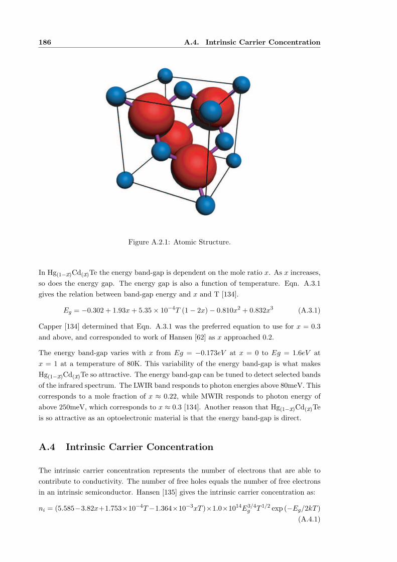
186 A.4. Intrinsic Carrier Concentration
Figure A.2.1: Atomic Structure.
In Hg(1−x)Cd(x)Te the energy band-gap is dependent on the mole ratio x. As x increases,
so does the energy gap. The energy gap is also a function of temperature. Eqn. A.3.1
gives the relation between band-gap energy and x and T [134].
Eg = −0.302 + 1.93x+ 5.35 × 10⁻⁴T (1 − 2x) − 0.810x2 + 0.832x3 (A.3.1)
Capper [134] determined that Eqn. A.3.1 was the preferred equation to use for x = 0.3
and above, and corresponded to work of Hansen [62] as x approached 0.2.
The energy band-gap varies with x from Eg = −0.173eV at x = 0 to Eg = 1.6eV at
x = 1 at a temperature of 80K. This variability of the energy band-gap is what makes
Hg(1−x)Cd(x)Te so attractive. The energy band-gap can be tuned to detect selected bands
of the infrared spectrum. The LWIR band responds to photon energies above 80meV. This
corresponds to a mole fraction of x ≈ 0.22, while MWIR responds to photon energy of
above 250meV, which corresponds to x ≈ 0.3 [134]. Another reason that Hg(1−x)Cd(x)Te
is so attractive as an optoelectronic material is that the energy band-gap is direct.
A.4 Intrinsic Carrier Concentration
The intrinsic carrier concentration represents the number of electrons that are able to
contribute to conductivity. The number of free holes equals the number of free electrons
in an intrinsic semiconductor. Hansen [135] gives the intrinsic carrier concentration as:
ni = (5.585−3.82x+1.753×10⁻⁴T−1.364×10⁻³xT )×1.0×10¹⁴E3/4g T 1/2 exp (−Eg/2kT )
(A.4.1)
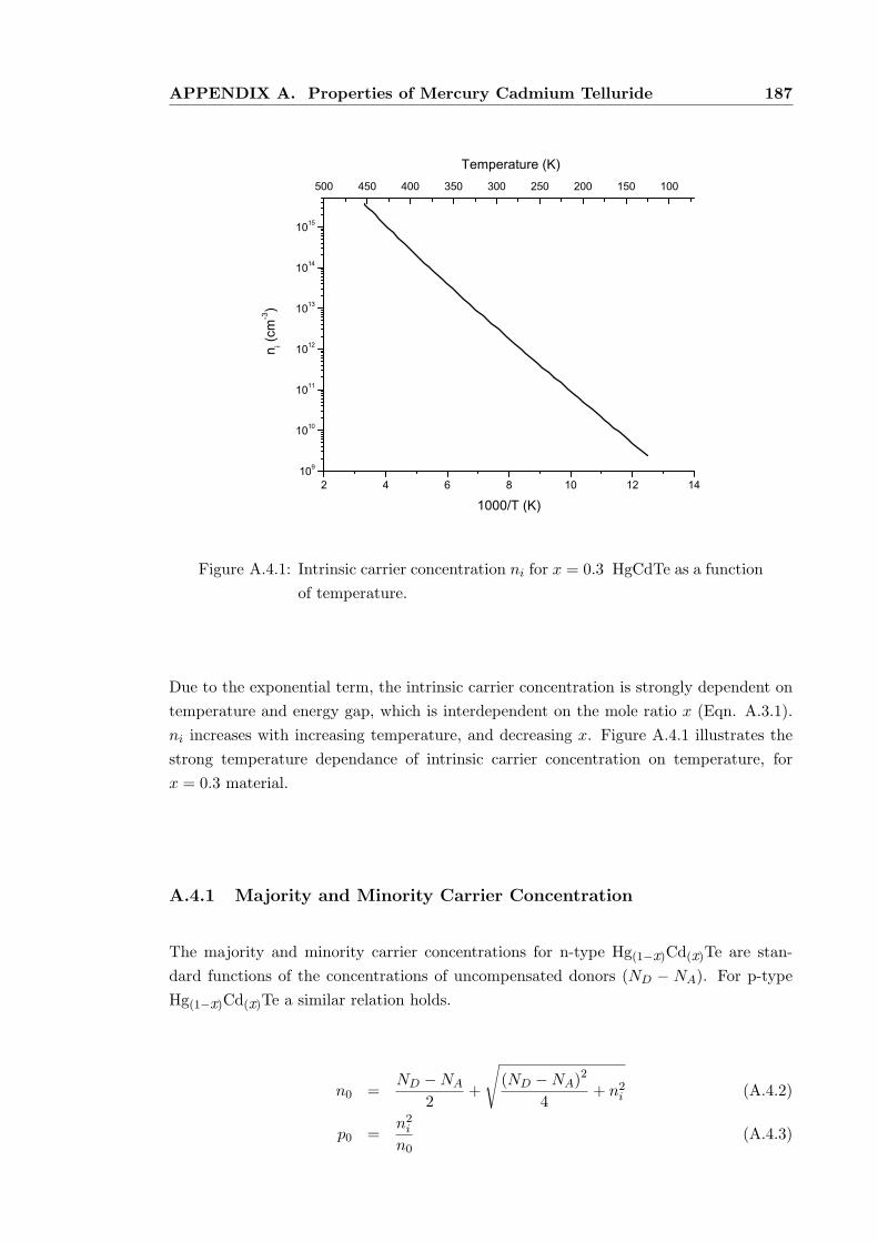
APPENDIX A. Properties of Mercury Cadmium Telluride 187
2 4 6 8 10 12 14109
1010
1011
1012
1013
1014
1015
500 450 400 350 300 250 200 150 100
n i (cm
-3)
1000/T (K)
Temperature (K)
Figure A.4.1: Intrinsic carrier concentration ni for x = 0.3 HgCdTe as a function
of temperature.
Due to the exponential term, the intrinsic carrier concentration is strongly dependent on
temperature and energy gap, which is interdependent on the mole ratio x (Eqn. A.3.1).
ni increases with increasing temperature, and decreasing x. Figure A.4.1 illustrates the
strong temperature dependance of intrinsic carrier concentration on temperature, for
x = 0.3 material.
A.4.1 Majority and Minority Carrier Concentration
The majority and minority carrier concentrations for n-type Hg(1−x)Cd(x)Te are stan-
dard functions of the concentrations of uncompensated donors (ND − NA). For p-type
Hg(1−x)Cd(x)Te a similar relation holds.
n0 =ND −NA
2+
√
(ND −NA)2
4+ n2
i (A.4.2)
p0 =n2
i
n0(A.4.3)
188 A.5. Effective Mass
A.5 Effective Mass
For Hg(1−x)Cd(x)Te, the electron effective mass is determined to be [136]:
m∗e = m0 exp
[
4
3log
ni
3.126 × 10¹⁵T3
2 exp−Eg
2kT
]
(A.5.1)
Alternatively, the ratio of the rest mass of an electron to the effective electron mass is
given by [137]:
m0
m∗e
= 1 +8m0P
2π2
3h2 [(2/Eg) + (1/ (Eg + ∆))](A.5.2)
where P is the Kane momentum matrix element, related to inter-band energy (Ep), by
Ep = 8m0P2π2/h2, and can be assumed to be around 19eV.
The mass of the heavy hole is taken as [137]:
mh = 0.55m0 (A.5.3)
A.6 Mobility
Mobility (cm2/V s)is a measure of how fast or how easily carriers drift (how much they
are affected by an electric field), and is equal to the drift velocity per unit applied electric
field. Mobility is affected by scattering (lattice and impurity scattering are the main
types), which causes the carriers to lose kinetic energy imparted by the applied field. Hall
measurements by Scott et al. [138] lead to an approximation of µ for 0.2 ≤ x ≤ 0.6:
µn =9 × 10⁸b
Z2a(A.6.1)
where:
b =(
0.2x
7.5)
a =(
0.2x
0.6)
for:
T > 50K;Z = T
T ≤ 50K; Z = 1.18×10⁵
2600−|T−35|2.07
Mobility is dependent on temperature, as given in Eqn. A.6.1 and shown in Fig. A.6.1.
As can be seen in this figure, for temperatures above 40K the mobility decreases sharply
due to increased phonon scattering. For temperatures below 40K, the mobility is limited
by impurity scattering.
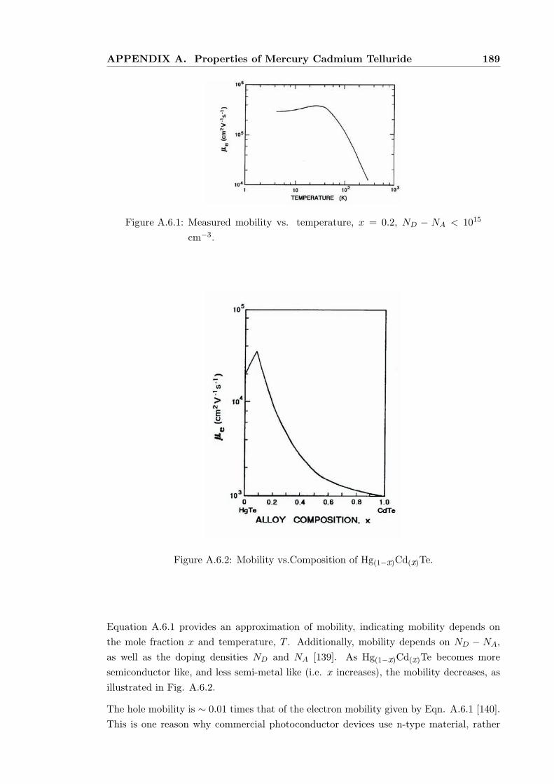
APPENDIX A. Properties of Mercury Cadmium Telluride 189
Figure A.6.1: Measured mobility vs. temperature, x = 0.2, ND − NA < 1015
cm−3.
Figure A.6.2: Mobility vs.Composition of Hg(1−x)Cd(x)Te.
Equation A.6.1 provides an approximation of mobility, indicating mobility depends on
the mole fraction x and temperature, T . Additionally, mobility depends on ND − NA,
as well as the doping densities ND and NA [139]. As Hg(1−x)Cd(x)Te becomes more
semiconductor like, and less semi-metal like (i.e. x increases), the mobility decreases, as
illustrated in Fig. A.6.2.
The hole mobility is ∼ 0.01 times that of the electron mobility given by Eqn. A.6.1 [140].
This is one reason why commercial photoconductor devices use n-type material, rather
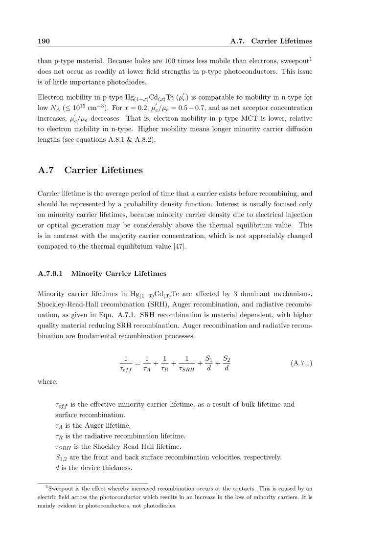
190 A.7. Carrier Lifetimes
than p-type material. Because holes are 100 times less mobile than electrons, sweepout1
does not occur as readily at lower field strengths in p-type photoconductors. This issue
is of little importance photodiodes.
Electron mobility in p-type Hg(1−x)Cd(x)Te (µ′
e) is comparable to mobility in n-type for
low NA (≤ 1015 cm−3). For x = 0.2, µ′
e/µe = 0.5−0.7, and as net acceptor concentration
increases, µ′
e/µe decreases. That is, electron mobility in p-type MCT is lower, relative
to electron mobility in n-type. Higher mobility means longer minority carrier diffusion
lengths (see equations A.8.1 & A.8.2).
A.7 Carrier Lifetimes
Carrier lifetime is the average period of time that a carrier exists before recombining, and
should be represented by a probability density function. Interest is usually focused only
on minority carrier lifetimes, because minority carrier density due to electrical injection
or optical generation may be considerably above the thermal equilibrium value. This
is in contrast with the majority carrier concentration, which is not appreciably changed
compared to the thermal equilibrium value [47].
A.7.0.1 Minority Carrier Lifetimes
Minority carrier lifetimes in Hg(1−x)Cd(x)Te are affected by 3 dominant mechanisms,
Shockley-Read-Hall recombination (SRH), Auger recombination, and radiative recombi-
nation, as given in Eqn. A.7.1. SRH recombination is material dependent, with higher
quality material reducing SRH recombination. Auger recombination and radiative recom-
bination are fundamental recombination processes.
1
τeff=
1
τA+
1
τR+
1
τSRH+S1
d+S2
d(A.7.1)
where:
τeff is the effective minority carrier lifetime, as a result of bulk lifetime and
surface recombination.
τA is the Auger lifetime.
τR is the radiative recombination lifetime.
τSRH is the Shockley Read Hall lifetime.
S1,2 are the front and back surface recombination velocities, respectively.
d is the device thickness.
1Sweepout is the effect whereby increased recombination occurs at the contacts. This is caused by an
electric field across the photoconductor which results in an increase in the loss of minority carriers. It is
mainly evident in photoconductors, not photodiodes.
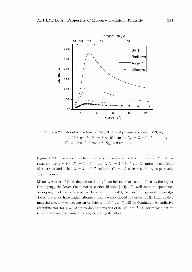
APPENDIX A. Properties of Mercury Cadmium Telluride 191
4 6 8 10 120.0
10.0µ
20.0µ
30.0µ
40.0µ
50.0µ
60.0µ
300 250 200 150 100
Life
time
(s)
1000/T (K-1)
SRH
Radiative
Auger 1
Effective
Temperature (K)
Figure A.7.1: Modelled lifetime vs. 1000/T. Model parameters are x = 0.3, Nd =
1 × 1015 cm−3, Nt = 3 × 1013 cm−3, Cp = 3 × 10⁻⁹ cm3 s−1,
Cn = 1.9 × 10⁻⁷ cm3 s−1, S1,2 = 0 cm s−1.
Figure A.7.1 illustrates the effect that varying temperature has on lifetime. Model pa-
rameters are x = 0.3, Nd = 1 × 1015 cm−3, Nt = 3 × 1013 cm−3, capture coefficients
of electrons and holes Cp = 3 × 10⁻⁹ cm3 s−1, Cn = 1.9 × 10⁻⁷ cm3 s−1, respectively,
S1,2 = 0 cm s−1.
Minority carrier lifetimes depend on doping in an inverse relationship. That is, the higher
the doping, the lower the minority carrier lifetime [141]. As well as this dependence
on doping, lifetime is related to the specific dopant type used. In general, impurity-
doped materials have higher lifetimes than vacancy-doped materials [141]. High quality
material (i.e. low concentration of defects < 1014 cm−3) will be dominated by radiative
recombination for x = 0.3 up to doping densities of ≈ 1015 cm−3. Auger recombination
is the dominant mechanism for higher doping densities.
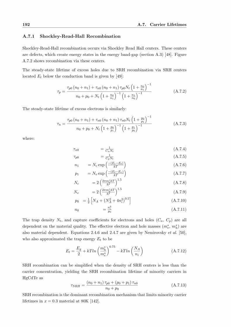
192 A.7. Carrier Lifetimes
A.7.1 Shockley-Read-Hall Recombination
Shockley-Read-Hall recombination occurs via Shockley Read Hall centers. These centers
are defects, which create energy states in the energy band-gap (section A.3) [48]. Figure
A.7.2 shows recombination via these centers.
The steady-state lifetime of excess holes due to SRH recombination via SRH centers
located Et below the conduction band is given by [49]:
τp =τp0 (n0 + n1) + τn0 (n0 + n1) τp0Nt
(
1 + n0
n1
)−1
n0 + p0 +Nt
(
1 + n0
n1
)−1 (
1 + n1
n0
)−1 (A.7.2)
The steady-state lifetime of excess electrons is similarly:
τn =τp0 (n0 + n1) + τn0 (n0 + n1) τn0Nt
(
1 + p0
p1
)−1
n0 + p0 +Nt
(
1 + p0
p1
)−1 (
1 + p1
p0
)−1 (A.7.3)
where:
τn0 = 1CnNt
(A.7.4)
τp0 = 1CpNt
(A.7.5)
n1 = Nc exp(
−(Ec−Et)kT
)
(A.7.6)
p1 = Nv exp(
−(Et−Ev)kT
)
(A.7.7)
Nc = 2(
2πm∗
ekTh2
)1.5(A.7.8)
Nv = 2(
2πm∗
hkT
h2
)1.5(A.7.9)
p0 = 12
[
NA +(
N2A + 4n2
i
)0.5]
(A.7.10)
n0 =n2
i
p0(A.7.11)
The trap density Nt, and capture coefficients for electrons and holes (Cn, Cp) are all
dependent on the material quality. The effective electron and hole masses (m∗e, m
∗h) are
also material dependent. Equations 2.4.6 and 2.4.7 are given by Nemirovsky et al. [50],
who also approximated the trap energy Et to be
Et =Eg
2+ kT ln
(
m∗h
m∗e
)0.75
− kT ln
(
NA
ni
)
(A.7.12)
SRH recombination can be simplified when the density of SRH centers is less than the
carrier concentration, yielding the SRH recombination lifetime of minority carriers in
HgCdTe as
τSRH =(n0 + n1) τp0 + (p0 + p1) τn0
n0 + p0(A.7.13)
SRH recombination is the dominant recombination mechanism that limits minority carrier
lifetimes in x = 0.3 material at 80K [142].

APPENDIX A. Properties of Mercury Cadmium Telluride 193
A.7.2 Auger Recombination
Auger recombination is a direct recombination mechanism. In Hg(1−x)Cd(x)Te Auger
recombination occurs in two dominant combinations, shown in Fig. A.7.3:
• Auger1: direct band-to-band recombination of electron with heavy hole and excite-
ment of another electron in conduction band. This is the dominant mechanism in
n-type material.
• Auger7: direct band-to-band recombination of electron and excitation of electron
from light hole to heavy hole band [48]. This is the dominant mechanism in p-type
material.
In high-quality n-type Hg(1−x)Cd(x)Te at 80K the lifetime is determined by Auger1 re-
combination [143]:
τA1 =2τA1in
2i
n0 (n0 + p0)(A.7.14)
τA1i = 3.8 × 10⁻¹⁸ε2∞m0
m∗e
(
1 +m0
mh
)2 (
1 + 2m0
mh
)(
Eg
kT
)3
2
× exp
(
1 + 2m0
mh
)
(
1 + m0
mh
)
Eg
kT× |f1f2|−2 (A.7.15)
where:
ε∞ is the high frequency permittivity and is taken as
ε∞ = 15.2 − 15.6 × x+ 8.2 × x2.
|f1f2| is the overlap function from the Bloch integral and for Hg(1−x)Cd(x)Te
a value of 0.15 is assumed.
Similarly, for Auger7 recombination the lifetime is given by:
τA7 =2τA7in
2i
p0 (n0 + p0)(A.7.16)
where:
τA7i = γτA1i
γ = ratio between Auger1 and Auger7 intrinsic lifetimes.
Combining Auger1 and Auger7 gives the complete Auger lifetime expression as:
1
τA=
1
τA1+
1
τA7(A.7.17)
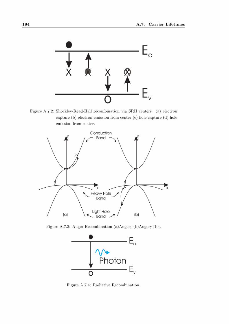
194 A.7. Carrier Lifetimes
x x x x
EcEc
Ev
Figure A.7.2: Shockley-Read-Hall recombination via SRH centers. (a) electron
capture (b) electron emission from center (c) hole capture (d) hole
emission from center.
E
k
E
k
ConductionBand
Heavy HoleBand
Light HoleBand(a) (b)
Figure A.7.3: Auger Recombination (a)Auger1 (b)Auger7 [10].
EcEc
Ev
Photon
Figure A.7.4: Radiative Recombination.
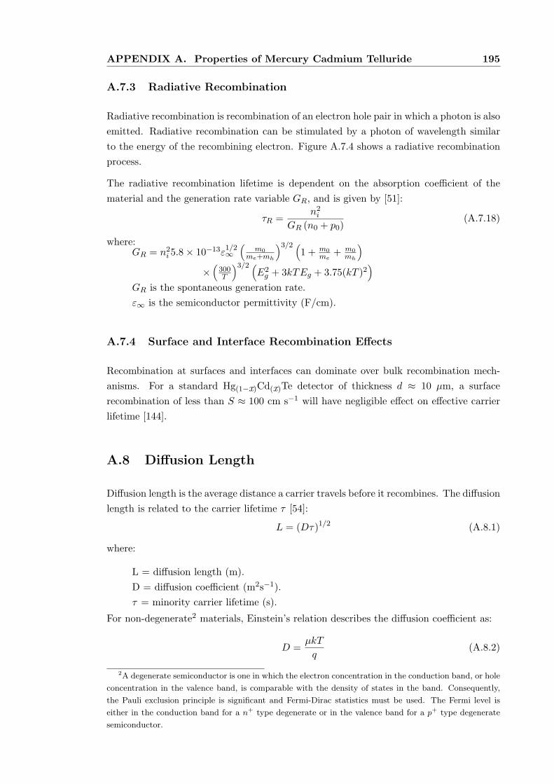
APPENDIX A. Properties of Mercury Cadmium Telluride 195
A.7.3 Radiative Recombination
Radiative recombination is recombination of an electron hole pair in which a photon is also
emitted. Radiative recombination can be stimulated by a photon of wavelength similar
to the energy of the recombining electron. Figure A.7.4 shows a radiative recombination
process.
The radiative recombination lifetime is dependent on the absorption coefficient of the
material and the generation rate variable GR, and is given by [51]:
τR =n2
i
GR (n0 + p0)(A.7.18)
where:GR = n2
i 5.8 × 10⁻¹³ε1/2∞
(
m0
me+mh
)3/2 (
1 + m0
me+ m0
mh
)
×(
300T
)3/2 (
E2g + 3kTEg + 3.75(kT )2
)
GR is the spontaneous generation rate.
ε∞ is the semiconductor permittivity (F/cm).
A.7.4 Surface and Interface Recombination Effects
Recombination at surfaces and interfaces can dominate over bulk recombination mech-
anisms. For a standard Hg(1−x)Cd(x)Te detector of thickness d ≈ 10 µm, a surface
recombination of less than S ≈ 100 cm s−1 will have negligible effect on effective carrier
lifetime [144].
A.8 Diffusion Length
Diffusion length is the average distance a carrier travels before it recombines. The diffusion
length is related to the carrier lifetime τ [54]:
L = (Dτ)1/2 (A.8.1)
where:
L = diffusion length (m).
D = diffusion coefficient (m2s−1).
τ = minority carrier lifetime (s).
For non-degenerate2 materials, Einstein’s relation describes the diffusion coefficient as:
D =µkT
q(A.8.2)
2A degenerate semiconductor is one in which the electron concentration in the conduction band, or hole
concentration in the valence band, is comparable with the density of states in the band. Consequently,
the Pauli exclusion principle is significant and Fermi-Dirac statistics must be used. The Fermi level is
either in the conduction band for a n+ type degenerate or in the valence band for a p
+ type degenerate
semiconductor.
196 A.9. Refractive Index of HgCdTe
A.9 Refractive Index of HgCdTe
A.9.1 Refractive Index
The real part of the refractive index used in this work is described by Capper [56] and
modified by Daraselia et al. [116]
n(λ)2 = a1 +a2a
23
(
a23 − 1
λ2
)
(
a23 − 1
λ2
)2+(
dfλ
)+
a4λ2
λ2 − a25
(A.9.1)
Table A.9.1: Fitting parameters for Eqn. A.9.1
Coefficient Ai Bi Ci
a1 19.76 -41.82 34.50
a2 0.373 -0.281 2.153
a3 -0.005 0.532 1.897
a1 18.79 -58.40 52.41
A.9.2 Extinction Co-efficient
The extinction co-efficient is derived from the absorption model of Price [63]:
α (E) =
α0 exp(
σ(E−E0)T+T0
)
α ≤ 500 + 5600x = αT
β√
E − Eg α > 500 + 5600x(A.9.2)
k (E) = α (E) ∗ λ
4π ∗ n (A.9.3)
Where :
ai = Ai +Bix+ Cix2 (i = 1, 2, 3, 4)
a5 = 73.25 µm
α0 = exp (−18.88 + 53.61x) (A.9.4)
σ = 3.267 × 10⁴ (1 + x) (A.9.5)
E0 = −0.3424 + 1.838x (A.9.6)
Eg = log
(
αT
α0√e
)(
T + T0
σ
)
+ E0 (A.9.7)
β =αT
(
T + T0
2σ
)1/2(A.9.8)
T0 = 81.9 K
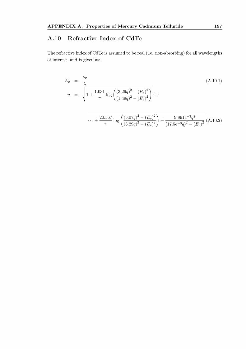
APPENDIX A. Properties of Mercury Cadmium Telluride 197
A.10 Refractive Index of CdTe
The refractive index of CdTe is assumed to be real (i.e. non-absorbing) for all wavelengths
of interest, and is given as:
Ev =hc
λ(A.10.1)
n =
√
√
√
√1 +1.031
πlog
(
(3.29q)2 − (Ev)2
(1.49q)2 − (Ev)2
)
· · ·
· · · + 20.567
πlog
(
(5.07q)2 − (Ev)2
(3.29q)2 − (Ev)2
)
+9.891e−3q2
(17.5e−3q)2 − (Ev)2 (A.10.2)

198 A.10. Refractive Index of CdTe
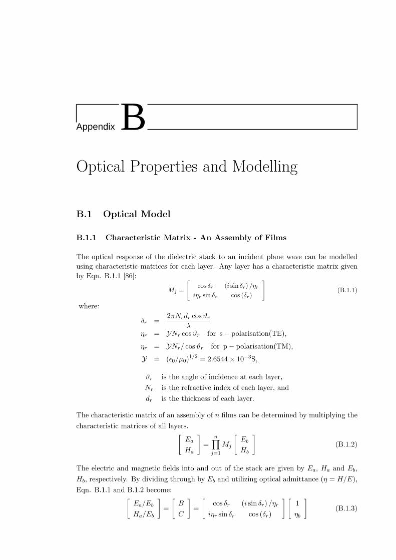
Appendix BOptical Properties and Modelling
B.1 Optical Model
B.1.1 Characteristic Matrix - An Assembly of Films
The optical response of the dielectric stack to an incident plane wave can be modelled
using characteristic matrices for each layer. Any layer has a characteristic matrix given
by Eqn. B.1.1 [86]:
Mj =
[
cos δr (i sin δr) /ηr
iηr sin δr cos (δr)
]
(B.1.1)
where:
δr =2πNrdr cosϑr
ληr = YNr cosϑr for s − polarisation(TE),
ηr = YNr/ cosϑr for p − polarisation(TM),
Y = (ǫ0/µ0)1/2 = 2.6544 × 10⁻³S,
ϑr is the angle of incidence at each layer,
Nr is the refractive index of each layer, and
dr is the thickness of each layer.
The characteristic matrix of an assembly of n films can be determined by multiplying the
characteristic matrices of all layers.[
Ea
Ha
]
=n∏
j=1
Mj
[
Eb
Hb
]
(B.1.2)
The electric and magnetic fields into and out of the stack are given by Ea, Ha and Eb,
Hb, respectively. By dividing through by Eb and utilizing optical admittance (η = H/E),
Eqn. B.1.1 and B.1.2 become:[
Ea/Eb
Ha/Eb
]
=
[
B
C
]
=
[
cos δr (i sin δr) /ηr
iηr sin δr cos (δr)
] [
1
ηb
]
(B.1.3)
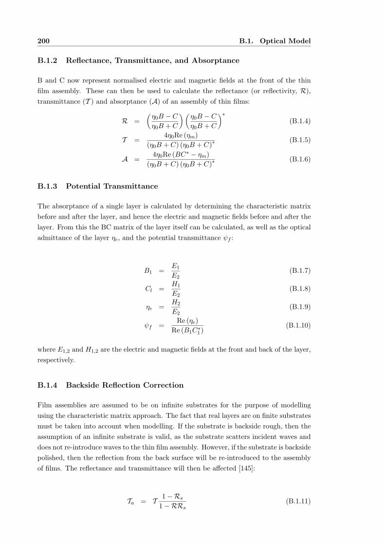
200 B.1. Optical Model
B.1.2 Reflectance, Transmittance, and Absorptance
B and C now represent normalised electric and magnetic fields at the front of the thin
film assembly. These can then be used to calculate the reflectance (or reflectivity, R),
transmittance (T ) and absorptance (A) of an assembly of thin films:
R =
(
η0B − C
η0B + C
)(
η0B − C
η0B + C
)∗
(B.1.4)
T =4η0Re (ηm)
(η0B + C) (η0B + C)∗(B.1.5)
A =4η0Re (BC∗ − ηm)
(η0B + C) (η0B + C)∗(B.1.6)
B.1.3 Potential Transmittance
The absorptance of a single layer is calculated by determining the characteristic matrix
before and after the layer, and hence the electric and magnetic fields before and after the
layer. From this the BC matrix of the layer itself can be calculated, as well as the optical
admittance of the layer ηe, and the potential transmittance ψf :
B1 =E1
E2(B.1.7)
Cl =H1
E2(B.1.8)
ηe =H2
E2(B.1.9)
ψf =Re (ηe)
Re (B1C∗1 )
(B.1.10)
where E1,2 and H1,2 are the electric and magnetic fields at the front and back of the layer,
respectively.
B.1.4 Backside Reflection Correction
Film assemblies are assumed to be on infinite substrates for the purpose of modelling
using the characteristic matrix approach. The fact that real layers are on finite substrates
must be taken into account when modelling. If the substrate is backside rough, then the
assumption of an infinite substrate is valid, as the substrate scatters incident waves and
does not re-introduce waves to the thin film assembly. However, if the substrate is backside
polished, then the reflection from the back surface will be re-introduced to the assembly
of films. The reflectance and transmittance will then be affected [145]:
Ta = T 1 −Rs
1 −RRs(B.1.11)

APPENDIX B. Optical Properties and Modelling 201
Ra = R +R2Rs
1 −RRs(B.1.12)
Rs =
(
ns − ni
ns + ni
)(
ns − ni
ns + ni
)∗
(B.1.13)
where Ra and Ta are the adjusted reflectance and transmittance, R and T are the re-
flectance and transmittance of the thin film assembly, and Rs is the reflection of the
substrate/incident material interface at the back surface, and depends on the refractive
index of the substrate, ns, and incident media, ni.

202 B.1. Optical Model
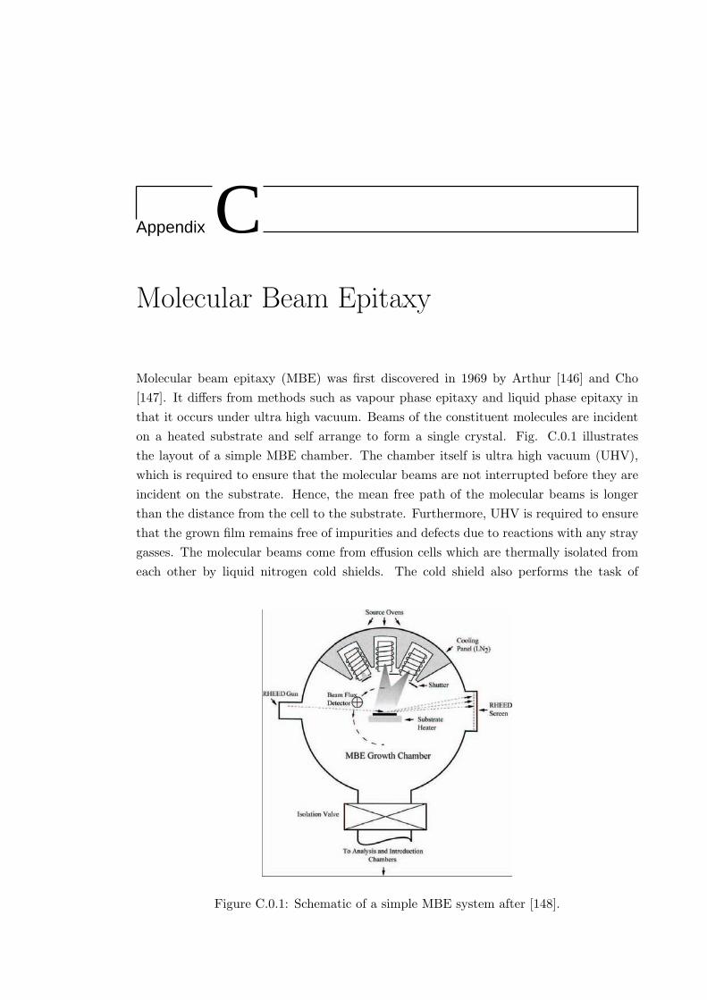
Appendix CMolecular Beam Epitaxy
Molecular beam epitaxy (MBE) was first discovered in 1969 by Arthur [146] and Cho
[147]. It differs from methods such as vapour phase epitaxy and liquid phase epitaxy in
that it occurs under ultra high vacuum. Beams of the constituent molecules are incident
on a heated substrate and self arrange to form a single crystal. Fig. C.0.1 illustrates
the layout of a simple MBE chamber. The chamber itself is ultra high vacuum (UHV),
which is required to ensure that the molecular beams are not interrupted before they are
incident on the substrate. Hence, the mean free path of the molecular beams is longer
than the distance from the cell to the substrate. Furthermore, UHV is required to ensure
that the grown film remains free of impurities and defects due to reactions with any stray
gasses. The molecular beams come from effusion cells which are thermally isolated from
each other by liquid nitrogen cold shields. The cold shield also performs the task of
Figure C.0.1: Schematic of a simple MBE system after [148].
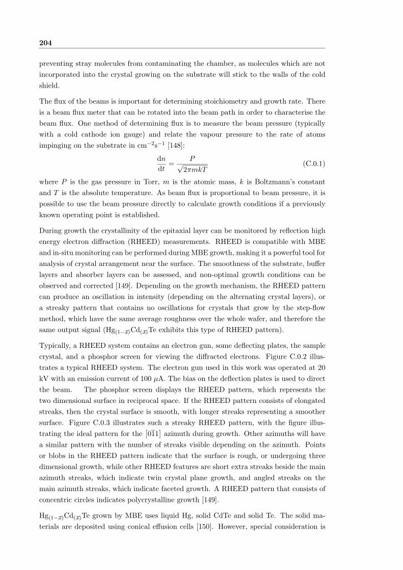
204
preventing stray molecules from contaminating the chamber, as molecules which are not
incorporated into the crystal growing on the substrate will stick to the walls of the cold
shield.
The flux of the beams is important for determining stoichiometry and growth rate. There
is a beam flux meter that can be rotated into the beam path in order to characterise the
beam flux. One method of determining flux is to measure the beam pressure (typically
with a cold cathode ion gauge) and relate the vapour pressure to the rate of atoms
impinging on the substrate in cm−2s−1 [148]:
dn
dt=
P√2πmkT
(C.0.1)
where P is the gas pressure in Torr, m is the atomic mass, k is Boltzmann’s constant
and T is the absolute temperature. As beam flux is proportional to beam pressure, it is
possible to use the beam pressure directly to calculate growth conditions if a previously
known operating point is established.
During growth the crystallinity of the epitaxial layer can be monitored by reflection high
energy electron diffraction (RHEED) measurements. RHEED is compatible with MBE
and in-situ monitoring can be performed during MBE growth, making it a powerful tool for
analysis of crystal arrangement near the surface. The smoothness of the substrate, buffer
layers and absorber layers can be assessed, and non-optimal growth conditions can be
observed and corrected [149]. Depending on the growth mechanism, the RHEED pattern
can produce an oscillation in intensity (depending on the alternating crystal layers), or
a streaky pattern that contains no oscillations for crystals that grow by the step-flow
method, which have the same average roughness over the whole wafer, and therefore the
same output signal (Hg(1−x)Cd(x)Te exhibits this type of RHEED pattern).
Typically, a RHEED system contains an electron gun, some deflecting plates, the sample
crystal, and a phosphor screen for viewing the diffracted electrons. Figure C.0.2 illus-
trates a typical RHEED system. The electron gun used in this work was operated at 20
kV with an emission current of 100 µA. The bias on the deflection plates is used to direct
the beam. The phosphor screen displays the RHEED pattern, which represents the
two dimensional surface in reciprocal space. If the RHEED pattern consists of elongated
streaks, then the crystal surface is smooth, with longer streaks representing a smoother
surface. Figure C.0.3 illustrates such a streaky RHEED pattern, with the figure illus-
trating the ideal pattern for the[
011]
azimuth during growth. Other azimuths will have
a similar pattern with the number of streaks visible depending on the azimuth. Points
or blobs in the RHEED pattern indicate that the surface is rough, or undergoing three
dimensional growth, while other RHEED features are short extra streaks beside the main
azimuth streaks, which indicate twin crystal plane growth, and angled streaks on the
main azimuth streaks, which indicate faceted growth. A RHEED pattern that consists of
concentric circles indicates polycrystalline growth [149].
Hg(1−x)Cd(x)Te grown by MBE uses liquid Hg, solid CdTe and solid Te. The solid ma-
terials are deposited using conical effusion cells [150]. However, special consideration is
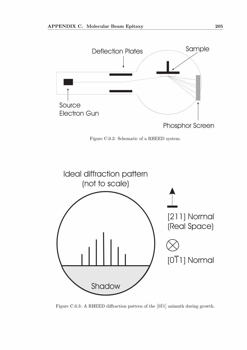
APPENDIX C. Molecular Beam Epitaxy 205
SourceElectron Gun
Deflection Plates
Phosphor Screen
Sample
Figure C.0.2: Schematic of a RHEED system.
[211] Normal(Real Space)
[0 1] Normal1
Shadow
Ideal diffraction pattern(not to scale)
Figure C.0.3: A RHEED diffraction pattern of the[
011]
azimuth during growth.
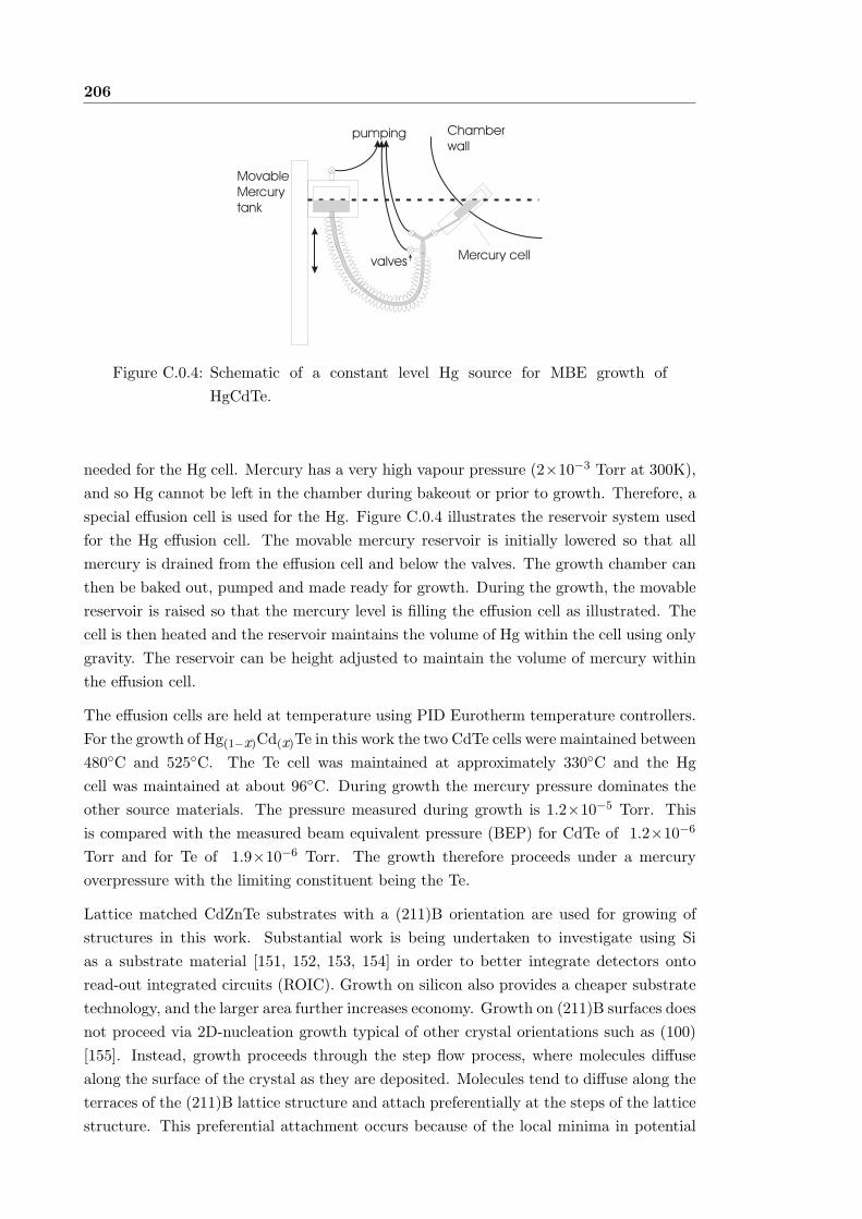
206
MovableMercurytank
Chamberwall
Mercury cell
pumping
valves
Figure C.0.4: Schematic of a constant level Hg source for MBE growth of
HgCdTe.
needed for the Hg cell. Mercury has a very high vapour pressure (2×10⁻³ Torr at 300K),
and so Hg cannot be left in the chamber during bakeout or prior to growth. Therefore, a
special effusion cell is used for the Hg. Figure C.0.4 illustrates the reservoir system used
for the Hg effusion cell. The movable mercury reservoir is initially lowered so that all
mercury is drained from the effusion cell and below the valves. The growth chamber can
then be baked out, pumped and made ready for growth. During the growth, the movable
reservoir is raised so that the mercury level is filling the effusion cell as illustrated. The
cell is then heated and the reservoir maintains the volume of Hg within the cell using only
gravity. The reservoir can be height adjusted to maintain the volume of mercury within
the effusion cell.
The effusion cells are held at temperature using PID Eurotherm temperature controllers.
For the growth of Hg(1−x)Cd(x)Te in this work the two CdTe cells were maintained between
480C and 525C. The Te cell was maintained at approximately 330C and the Hg
cell was maintained at about 96C. During growth the mercury pressure dominates the
other source materials. The pressure measured during growth is 1.2×10⁻⁵ Torr. This
is compared with the measured beam equivalent pressure (BEP) for CdTe of 1.2×10⁻⁶
Torr and for Te of 1.9×10⁻⁶ Torr. The growth therefore proceeds under a mercury
overpressure with the limiting constituent being the Te.
Lattice matched CdZnTe substrates with a (211)B orientation are used for growing of
structures in this work. Substantial work is being undertaken to investigate using Si
as a substrate material [151, 152, 153, 154] in order to better integrate detectors onto
read-out integrated circuits (ROIC). Growth on silicon also provides a cheaper substrate
technology, and the larger area further increases economy. Growth on (211)B surfaces does
not proceed via 2D-nucleation growth typical of other crystal orientations such as (100)
[155]. Instead, growth proceeds through the step flow process, where molecules diffuse
along the surface of the crystal as they are deposited. Molecules tend to diffuse along the
terraces of the (211)B lattice structure and attach preferentially at the steps of the lattice
structure. This preferential attachment occurs because of the local minima in potential
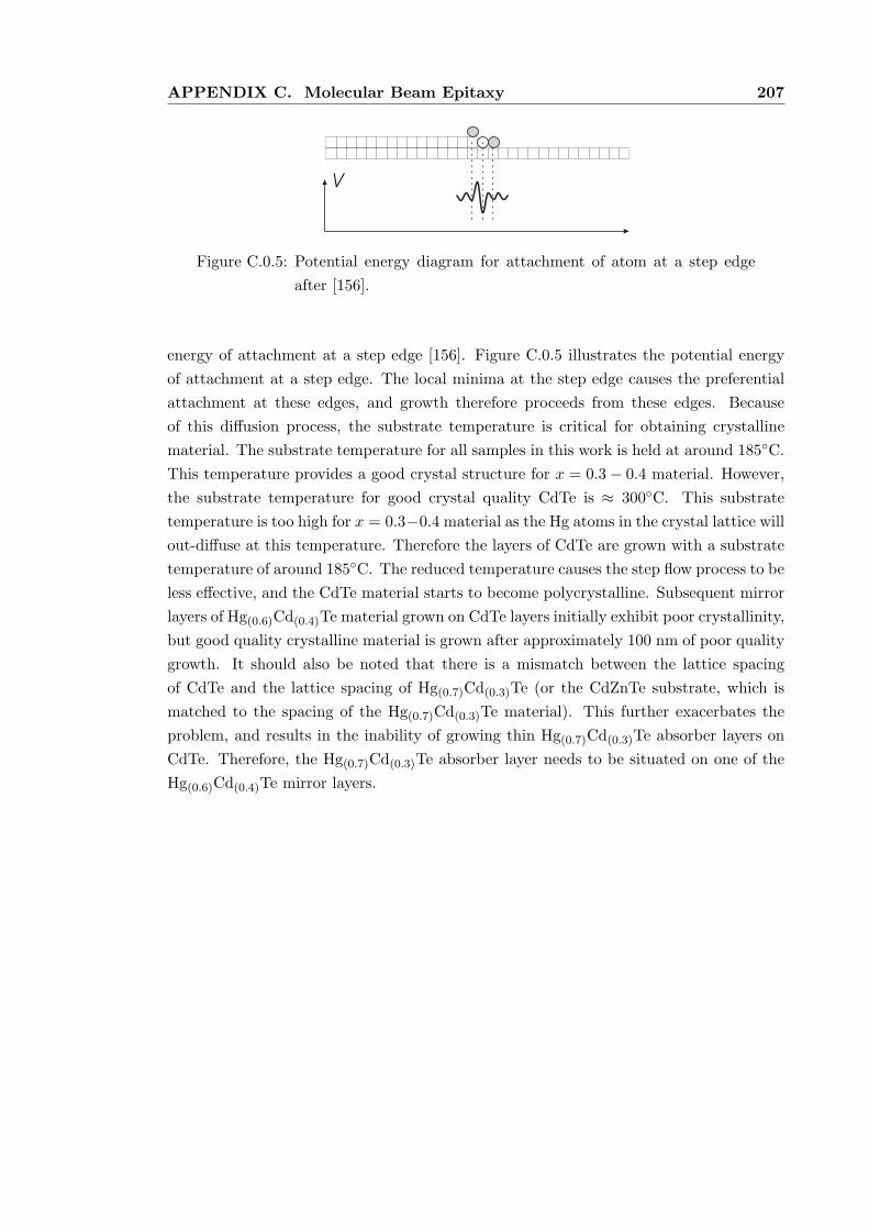
APPENDIX C. Molecular Beam Epitaxy 207
V
Figure C.0.5: Potential energy diagram for attachment of atom at a step edge
after [156].
energy of attachment at a step edge [156]. Figure C.0.5 illustrates the potential energy
of attachment at a step edge. The local minima at the step edge causes the preferential
attachment at these edges, and growth therefore proceeds from these edges. Because
of this diffusion process, the substrate temperature is critical for obtaining crystalline
material. The substrate temperature for all samples in this work is held at around 185C.
This temperature provides a good crystal structure for x = 0.3 − 0.4 material. However,
the substrate temperature for good crystal quality CdTe is ≈ 300C. This substrate
temperature is too high for x = 0.3−0.4 material as the Hg atoms in the crystal lattice will
out-diffuse at this temperature. Therefore the layers of CdTe are grown with a substrate
temperature of around 185C. The reduced temperature causes the step flow process to be
less effective, and the CdTe material starts to become polycrystalline. Subsequent mirror
layers of Hg(0.6)Cd(0.4)Te material grown on CdTe layers initially exhibit poor crystallinity,
but good quality crystalline material is grown after approximately 100 nm of poor quality
growth. It should also be noted that there is a mismatch between the lattice spacing
of CdTe and the lattice spacing of Hg(0.7)Cd(0.3)Te (or the CdZnTe substrate, which is
matched to the spacing of the Hg(0.7)Cd(0.3)Te material). This further exacerbates the
problem, and results in the inability of growing thin Hg(0.7)Cd(0.3)Te absorber layers on
CdTe. Therefore, the Hg(0.7)Cd(0.3)Te absorber layer needs to be situated on one of the
Hg(0.6)Cd(0.4)Te mirror layers.

208
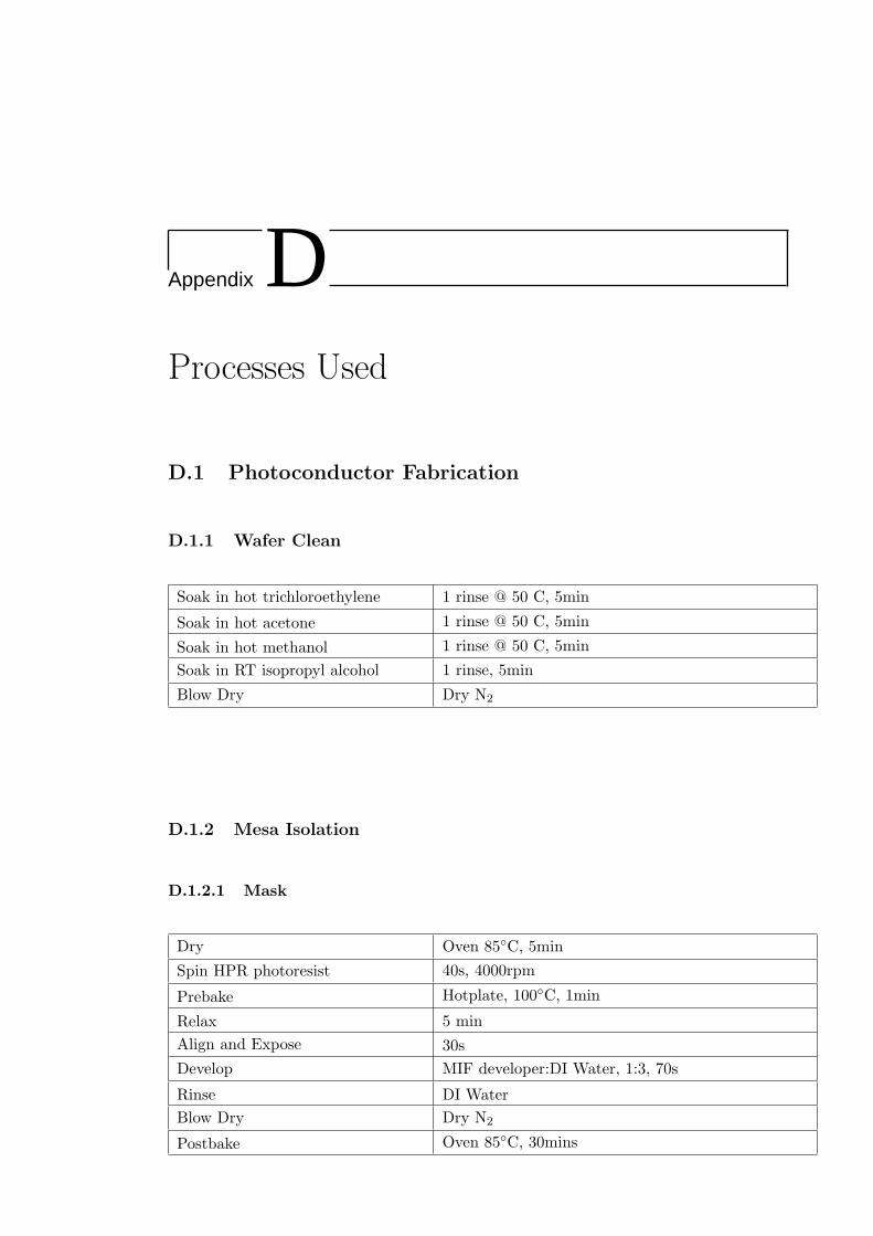
Appendix DProcesses Used
D.1 Photoconductor Fabrication
D.1.1 Wafer Clean
Soak in hot trichloroethylene 1 rinse @ 50 C, 5min
Soak in hot acetone 1 rinse @ 50 C, 5min
Soak in hot methanol 1 rinse @ 50 C, 5min
Soak in RT isopropyl alcohol 1 rinse, 5min
Blow Dry Dry N2
D.1.2 Mesa Isolation
D.1.2.1 Mask
Dry Oven 85C, 5min
Spin HPR photoresist 40s, 4000rpm
Prebake Hotplate, 100C, 1min
Relax 5 min
Align and Expose 30s
Develop MIF developer:DI Water, 1:3, 70s
Rinse DI Water
Blow Dry Dry N2
Postbake Oven 85C, 30mins
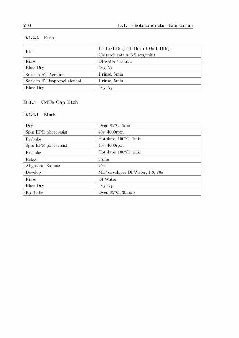
210 D.1. Photoconductor Fabrication
D.1.2.2 Etch
Etch1% Br/HBr (1mL Br in 100mL HBr),
90s (etch rate ≈ 3.9 µm/min)
Rinse DI water ≈10min
Blow Dry Dry N2
Soak in RT Acetone 1 rinse, 5min
Soak in RT isopropyl alcohol 1 rinse, 5min
Blow Dry Dry N2
D.1.3 CdTe Cap Etch
D.1.3.1 Mask
Dry Oven 85C, 5min
Spin HPR photoresist 40s, 4000rpm
Prebake Hotplate, 100C, 1min
Spin HPR photoresist 40s, 4000rpm
Prebake Hotplate, 100C, 1min
Relax 5 min
Align and Expose 40s
Develop MIF developer:DI Water, 1:3, 70s
Rinse DI Water
Blow Dry Dry N2
Postbake Oven 85C, 30mins
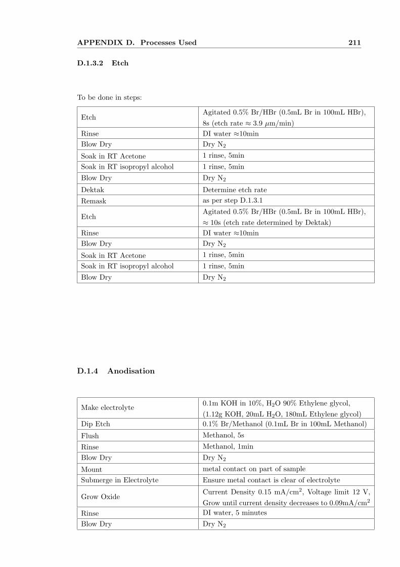
APPENDIX D. Processes Used 211
D.1.3.2 Etch
To be done in steps:
EtchAgitated 0.5% Br/HBr (0.5mL Br in 100mL HBr),
8s (etch rate ≈ 3.9 µm/min)
Rinse DI water ≈10min
Blow Dry Dry N2
Soak in RT Acetone 1 rinse, 5min
Soak in RT isopropyl alcohol 1 rinse, 5min
Blow Dry Dry N2
Dektak Determine etch rate
Remask as per step D.1.3.1
EtchAgitated 0.5% Br/HBr (0.5mL Br in 100mL HBr),
≈ 10s (etch rate determined by Dektak)
Rinse DI water ≈10min
Blow Dry Dry N2
Soak in RT Acetone 1 rinse, 5min
Soak in RT isopropyl alcohol 1 rinse, 5min
Blow Dry Dry N2
D.1.4 Anodisation
Make electrolyte0.1m KOH in 10%, H2O 90% Ethylene glycol,
(1.12g KOH, 20mL H2O, 180mL Ethylene glycol)
Dip Etch 0.1% Br/Methanol (0.1mL Br in 100mL Methanol)
Flush Methanol, 5s
Rinse Methanol, 1min
Blow Dry Dry N2
Mount metal contact on part of sample
Submerge in Electrolyte Ensure metal contact is clear of electrolyte
Grow OxideCurrent Density 0.15 mA/cm2, Voltage limit 12 V,
Grow until current density decreases to 0.09mA/cm2
Rinse DI water, 5 minutes
Blow Dry Dry N2

212 D.1. Photoconductor Fabrication
D.1.5 Oxide Etch
D.1.5.1 Mask
Dry Oven 85C, 5min
Spin HPR photoresist 40s, 4000rpm
Prebake Hotplate, 100C, 1min
Spin HPR photoresist 40s, 4000rpm
Prebake Hotplate, 100C, 1min
Relax 5 min
Align and Expose 40s
Develop MIF developer:DI Water, 1:3, 70s
Rinse DI Water
Blow Dry Dry N2
Postbake Oven 85C, 30mins
D.1.5.2 Etch
Dip Etch HCl:DI water, 1:3, 1 second
Rinse DI Water
Blow Dry Dry N2
Soak in RT Acetone 1 rinse, 5min
Soak in RT isopropyl alcohol 1 rinse, 5min
Blow Dry Dry N2
D.1.6 Metallisation
D.1.6.1 Metal Mask
Dry Oven 85C, 5min
Spin AZ2035 photoresist 40s, 2000rpm
Softbake Hotplate, 95C, 1min
Relax 5 min
Align and Expose 10s
Hardbake Hotplate, 110C, 1min
Develop 300MIF developer, neat, 120s
Rinse DI Water
Blow Dry Dry N2
Postbake Oven 85C, 30mins
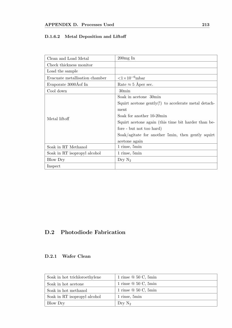
APPENDIX D. Processes Used 213
D.1.6.2 Metal Deposition and Liftoff
Clean and Load Metal 200mg In
Check thickness monitor
Load the sample
Evacuate metallisation chamber <1×10⁻⁶mbar
Evaporate 3000Aof In Rate ≈ 5 Aper sec.
Cool down 30min
Metal liftoff
Soak in acetone 30min
Squirt acetone gently(!) to accelerate metal detach-
ment
Soak for another 10-20min
Squirt acetone again (this time bit harder than be-
fore - but not too hard)
Soak/agitate for another 5min, then gently squirt
acetone again
Soak in RT Methanol 1 rinse, 5min
Soak in RT isopropyl alcohol 1 rinse, 5min
Blow Dry Dry N2
Inspect
D.2 Photodiode Fabrication
D.2.1 Wafer Clean
Soak in hot trichloroethylene 1 rinse @ 50 C, 5min
Soak in hot acetone 1 rinse @ 50 C, 5min
Soak in hot methanol 1 rinse @ 50 C, 5min
Soak in RT isopropyl alcohol 1 rinse, 5min
Blow Dry Dry N2
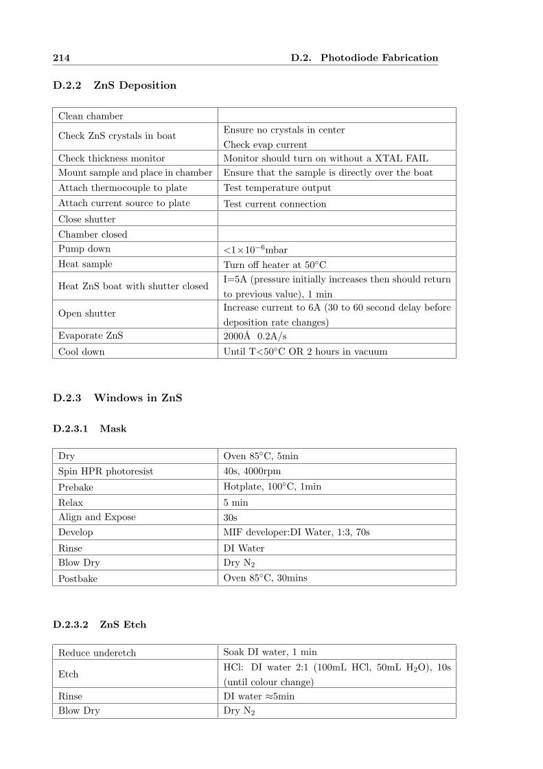
214 D.2. Photodiode Fabrication
D.2.2 ZnS Deposition
Clean chamber
Check ZnS crystals in boatEnsure no crystals in center
Check evap current
Check thickness monitor Monitor should turn on without a XTAL FAIL
Mount sample and place in chamber Ensure that the sample is directly over the boat
Attach thermocouple to plate Test temperature output
Attach current source to plate Test current connection
Close shutter
Chamber closed
Pump down <1×10⁻⁶mbar
Heat sample Turn off heater at 50C
Heat ZnS boat with shutter closedI=5A (pressure initially increases then should return
to previous value), 1 min
Open shutterIncrease current to 6A (30 to 60 second delay before
deposition rate changes)
Evaporate ZnS 2000A 0.2A/s
Cool down Until T<50C OR 2 hours in vacuum
D.2.3 Windows in ZnS
D.2.3.1 Mask
Dry Oven 85C, 5min
Spin HPR photoresist 40s, 4000rpm
Prebake Hotplate, 100C, 1min
Relax 5 min
Align and Expose 30s
Develop MIF developer:DI Water, 1:3, 70s
Rinse DI Water
Blow Dry Dry N2
Postbake Oven 85C, 30mins
D.2.3.2 ZnS Etch
Reduce underetch Soak DI water, 1 min
EtchHCl: DI water 2:1 (100mL HCl, 50mL H2O), 10s
(until colour change)
Rinse DI water ≈5min
Blow Dry Dry N2
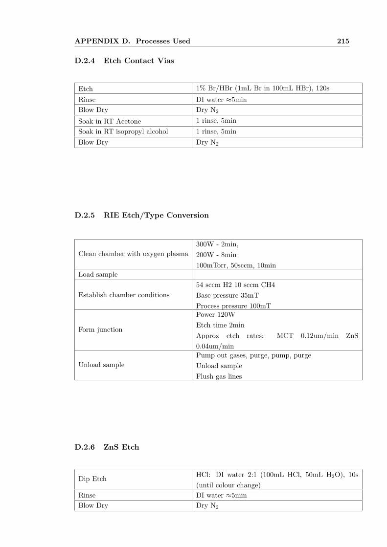
APPENDIX D. Processes Used 215
D.2.4 Etch Contact Vias
Etch 1% Br/HBr (1mL Br in 100mL HBr), 120s
Rinse DI water ≈5min
Blow Dry Dry N2
Soak in RT Acetone 1 rinse, 5min
Soak in RT isopropyl alcohol 1 rinse, 5min
Blow Dry Dry N2
D.2.5 RIE Etch/Type Conversion
Clean chamber with oxygen plasma
300W - 2min,
200W - 8min
100mTorr, 50sccm, 10min
Load sample
Establish chamber conditions
54 sccm H2 10 sccm CH4
Base pressure 35mT
Process pressure 100mT
Form junction
Power 120W
Etch time 2min
Approx etch rates: MCT 0.12um/min ZnS
0.04um/min
Unload sample
Pump out gases, purge, pump, purge
Unload sample
Flush gas lines
D.2.6 ZnS Etch
Dip EtchHCl: DI water 2:1 (100mL HCl, 50mL H2O), 10s
(until colour change)
Rinse DI water ≈5min
Blow Dry Dry N2

216 D.2. Photodiode Fabrication
D.2.7 Window for P Contact
D.2.7.1 Mask
Dry Oven 85C, 5min
Spin HPR photoresist 40s, 4000rpm
Prebake Hotplate, 100C, 1min
Spin HPR photoresist 40s, 4000rpm
Prebake Hotplate, 100C, 1min
Relax 5 min
Align and Expose 30s
Develop MIF developer : DI Water, 1:3, 70s
Rinse DI Water
Blow Dry Dry N2
Postbake Oven 85C, 30mins
D.2.7.2 Etch
Etch 1% Br/HBr (1mL Br in 100mL HBr), 120s
Rinse DI water ≈5min
Blow Dry Dry N2
Soak in RT Acetone 1 rinse, 5min
Soak in RT isopropyl alcohol 1 rinse, 5min
Blow Dry Dry N2
D.2.8 Metallisation
D.2.8.1 Metal Mask
Dry Oven 85C, 5min
Spin AZ2035 photoresist 40s, 2000rpm
Softbake Hotplate, 95C, 1min
Relax 5 min
Align and Expose 10s
Hardbake Hotplate, 110C, 1min
Develop 300MIF developer, neat, 120s
Rinse DI Water
Blow Dry Dry N2
Postbake Oven 85, 30mins

APPENDIX D. Processes Used 217
D.2.8.2 Metal Deposition and Liftoff
Load Cr and Au
Check thickness monitor
Load the sample
Evacuate metallisation chamber <1×10⁻⁶mbar
Evaporate 100 Aof Cr Rate ≈ 1 Aper sec.
Evaporate 3000Aof Au Rate ≈ 5 Aper sec.
Cool down 30min
Metal liftoff
Soak in acetone 30min
Squirt acetone gently(!) to accelerate metal detach-
ment
Soak for another 10-20min
Squirt acetone again (this time bit harder than be-
fore - but not too hard)
Soak/agitate for another 5min, then gently squirt
acetone again
Soak in RT Methanol 1 rinse, 5min
Soak in RT isopropyl alcohol 1 rinse, 5min
Blow Dry Dry N2
Inspect

218 D.2. Photodiode Fabrication
Appendix EAuthor’s Publications List
The following is a listing of the authors publications, including a division of the contribu-
tion. There is naturally guidance and support (financial and in the form of manuscript
revision, discussion etc.) from supervisors estimated at approximately 15-20% of the ef-
fort. Of the remaining effort, the divisions of each contributor are indicated, as well as
the details of contribution.
E.1 Journal Publications:
[1] Wehner J.G.A., Nguyen T.N., Antoszewski J., Musca C.A., Dell J.M., Faraone
L., Resonant Cavity-Enhanced Mercury Cadmium Telluride Detectors, J.
Electron. Mat. 33, 6; p. 604-608, 2004.
The percentage contribution of each author is as follows:
• Wehner J.G.A. 80%, All, except -
• Nguyen T.N. 10%, technical discussions and coding assistance.
• Antoszewski J. 5%, technical discussions.
• Musca C.A. 5%, technical discussions.
• Dell J.M. Supervisor.
• Faraone L. Supervisor.
[2] Wehner J.G.A. Sewell R.H., Antoszewski J., Musca C.A., Dell J.M., Faraone,
L. Mercury Cadmium Telluride/Cadmium Telluride Distributed Bragg Reflec-
tors for Use with Resonant Cavity Enhanced Detectors, J. Electron. Mat., 34,
6, pp. 710-715, 2005.
220 E.1. Journal Publications:
The percentage contribution of each author is as follows:
• Wehner J.G.A. 75%, All, except -
• Sewell R.H. 15%, technical discussions and growth assistance.
• Antoszewski J. 5%, technical discussions.
• Musca C.A. 5%, technical discussions.
• Dell J.M. Supervisor.
• Faraone L. Supervisor.
[3] Wehner J.G.A., Musca C.A., Sewell R.H., Dell J.M., Faraone L., Mercury
Cadmium Telluride Resonant Cavity Enhanced Photoconductive Infrared De-
tectors, Appl. Phys. Lett. 87, pp 211104, 2005.
The percentage contribution of each author is as follows:
• Wehner J.G.A. 75%, All, except -
• Musca C.A. 10%, technical discussions.
• Sewell R.H 15%, technical discussions and growth assistance.
• Dell J.M. Supervisor.
• Faraone L. Supervisor.
[4] Wehner J.G.A., Musca C.A., Sewell R.H., Dell J.M., and Faraone L., Respon-
sivity and Lifetime of Resonant-Cavity-Enhanced HgCdTe Detectors, Solid
State Electronics, 50, pp 16401648, 2006.
The percentage contribution of each author is as follows:
• Wehner J.G.A. 80%, All, except -
• Musca C.A. 10%, technical discussions.
• Sewell R.H 10%, technical discussions and growth assistance.
• Dell J.M. Supervisor.
• Faraone L. Supervisor.
APPENDIX E. Author’s Publications List 221
Accepted for Publication:
[5] Wehner J.G.A. Sewell R., Musca C.A., Dell J.M., Faraone, L. Refractive Index
Variations in MBE Grown CdTe for RCE Structures, Accepted 2/1/07 to J.
Electron. Mat..
The percentage contribution of each author is as follows:
• Wehner J.G.A. 45%, All, except -
• Sewell R.H 45%, x-ray measurements/writing , technical discussions and
all growth.
• Musca C.A. 10%, technical discussions.
• Dell J.M. Supervisor.
• Faraone L. Supervisor.
222 E.2. Conference Publications:
E.2 Conference Publications:
[1] Wehner J.G., Martyniuk M., Antoszewski J., Musca C.A., Dell J.M., Faraone
L. Optical and Membrane Modelling in a MEMS Hyper-spectral Imaging Sys-
tem, Conf. on Optoelectron. and Microelectron. Mat. And Dev.(COMMAD
2002), 11-13 Dec. 2002, UNSW, Sydney, Australia, IEEE Proc. 02EX 601,
pp. 579-582 (2002).
The percentage contribution of each author is as follows:
• Wehner J.G.A. 75%, All, except -
• Martyniuk M. 15%, Membrane images, technical discussion.
• Antoszewski J. 5%, technical discussions.
• Musca C.A. 5%, technical discussions.
• Dell J.M. Supervisor.
• Faraone L. Supervisor.
[2] Antoszewski J., Dell J.M., Shivakumar T., Martyniuk M., Winchester K.,
Wehner J., Musca C.A., Faraone L. Towards MEMS based infrared tun-
able micro-spectrometers, Smart Structures, Devices, and Systems, 16-18 Dec.
2002, RMIT, Melbourne, Australia, SPIE Proc. 4935, pp. 148-154 (2002).
The percentage contribution of this author is as follows:
• Wehner J.G.A. 5%, technical discussion.
[3] Wehner J.G.A., Sewell R., Antoszewski J., Musca C.A., Dell J.M., Faraone
L. Refractive Index Engineering for a Distributed Bragg Reflector for a Res-
onant Cavity Enhanced Detector, Design, Technology, and Packaging, Perth,
Australia, 10-12 Dec. 2003, SPIE Proc. 5277, pp. 138-145 (2004).
The percentage contribution of each author is as follows:
• Wehner J.G.A. 75%, All, except -
• Sewell R.H. 15%, technical discussions and modelling assistance.
• Antoszewski J. 5%, technical discussions.
• Musca C.A. 5%, technical discussions.
• Dell J.M. Supervisor.
• Faraone L. Supervisor.
[4] Wehner J.G.A, Sewell R.H., Musca C.A., Dell J.M., Faraone L. Responsivity
and Detectivity of Resonant Cavity Enhanced Mercury Cadmium Telluride
Infrared Detectors, Proceedings of Conf. on Optoelectron. and Microelec-
tron. Mat. and Dev. (COMMAD 2004), 8-10 Dec 2004, The University of
Queensland, Australia (2004).
APPENDIX E. Author’s Publications List 223
The percentage contribution of each author is as follows:
• Wehner J.G.A. 80%, All, except -
• Sewell R.H 15%, technical discussions and growth assistance.
• Musca C.A. 5%, technical discussions.
• Dell J.M. Supervisor.
• Faraone L. Supervisor.
[5] Wehner J.G.A., Sewell R.H., Musca C.A., Dell J.M., Faraone L. Resonant Cav-
ity Enhanced HgCdTe Detectors, Oral presentation IEEE Laser and Electro-
optic Society symposium 2005, Sydney, 23-27 Oct 2005 (2005).
The percentage contribution of each author is as follows:
• Wehner J.G.A. 80%, All, except -
• Sewell R.H 15%, technical discussions and growth assistance.
• Musca C.A. 5%, technical discussions.
• Dell J.M. Supervisor.
• Faraone L. Supervisor.
[6] Wehner J.G.A., Musca C.A., Sewell R.H., Dell J.M., Faraone L. Resonant
cavity enhanced HgCdTe photodetectors. Poster presentation at SPIE De-
fense and Security Symposium, Infrared Technology and Applications XXXII,
17-22 April 2006 at Gaylord Palms Resort and Convention Center in Orlando,
Florida, USA, SPIE Proc., pp. (2006).
The percentage contribution of each author is as follows:
• Wehner J.G.A. 75%, All, except -
• Musca C.A. 10%, technical discussions.
• Sewell R.H 15%, technical discussions and growth assistance.
• Dell J.M. Supervisor.
• Faraone L. Supervisor.
[7] Wehner J.G.A., Musca C.A., Sewell R.H., Dell J.M., Faraone L. Responsivity
and Lifetime of Resonant Cavity Enhanced HgCdTe detectors, 2006 IEEE
Aerospace Conf., Big Sky, 3-4 March 2006 Montana, USA (2006).
The percentage contribution of each author is as follows:
• Wehner J.G.A. 75%, All, except -
• Musca C.A. 10%, technical discussions.
• Sewell R.H 15%, technical discussions and growth assistance.
• Dell J.M. Supervisor.
• Faraone L. Supervisor.
224 E.2. Conference Publications:
Accepted Conference Presentations:
[8] Wehner J.G.A., Musca C.A., Sewell R.H., Dell J.M., Faraone L. Annealing
and Shunting in RCE HgCdTe Photoconductors, To be delivered: Conf. on
Optoelectron. and Microelectron. Mat. and Dev. (COMMAD 2006), 6-8 Dec
2006, The University of Western Australia, Australia (2006).
The percentage contribution of each author is as follows:
• Wehner J.G.A. 75%, All, except -
• Musca C.A. 10%, technical discussions.
• Sewell R.H 15%, technical discussions and growth assistance.
• Dell J.M. Supervisor.
• Faraone L. Supervisor.
Appendix FDetails of Contributions
The following is a listing of the contributions to the work presented:
Chapters 1 and 2
These are introductory chapters and all work is adequately referenced. Contribution in
the form of draft revision and proof reading by supervisors is acknowledged.
Chapter 3
Chapter 3 is an introductory chapter, however, it also contains modelling results published
in journal publication 1 in appendix E.
Chapter 4
Chapter 4 discusses mirror design and experimentation. There are results published in
journal publications 2 and 5 in appendix E. The results presented in section 4.4.2.2 are
based on measurements performed at the Australian Nuclear Science and Technology
Organisation (ANSTO), Lucas Heights by Gordon Tsen. Figure 4.4.10 is the work of
R.H. Sewell, and is the only work from journal publication 5 included that is not the
authors work.
Chapter 5
Chapter 5 discusses resonant-cavity-enhanced device design and experimentation. There
are results published in journal publications 1, 3 and 4 in appendix E, as well as results
published in conference proceedings 8.

226

“A witty saying proves nothing.” – Voltaire
+ =
“Ah, beer. The cause of and the solution to all of life’s problems.” –Homer J. Simpson

228
This final page has been left intentionally blank.
Recommended


![Justin Bieber The Key Eau du Parfum 100mL Justin Bieber ...files.shoppersdrugmart.ca/offers/justin-bieber/july2013/JB3_presell... · [ ] Justin Bieber The Key 100mL $70.00* [ ] Justin](https://img.pdfslide.us/doc/110x75/5e5cf67620150154c60a2919/justin-bieber-the-key-eau-du-parfum-100ml-justin-bieber-files-justin-bieber.jpg)