For price, delivery and to place orders: Hittite Microwave Corporation, 2 Elizabeth Drive, Chelmsford, MA 01824Phone: 978-250-3343 Fax: 978-250-3373 Order On-line at www.hittite.com
Application Support: Phone: 978-250-3343 or [email protected]
PLL
s w
ith
int
eg
rat
ed
VC
O -
sM
t
1
HMC830LP6GEv03.0512
Fractional-n Pll with integrated Vco25 - 3000 Mhz
Functional diagram
Features• rF Bandwidth: 25 - 3000 Mhz
• Maximum Phase detector rate 100 Mhz
• Ultra Low Phase noise -110 dBc/hz in Band typ.
• Figure of Merit (FOM) -227 dBc/hz
• <180 fs rMs Jitter
• 24-bit step size, resolution 3 hz typ
• exact Frequency Mode
• Built in digital self test
• 40 Lead 6x6 mm sMt Package: 36 mm2
typical applications
• Cellular/4g infrastructure
• repeaters and Femtocells
• Communications test equipment
• CatV equipment
• Phased array applications
• dds replacement
• Very high data rate radios
• tunable reference source for spurious- Free Performance
Information furnished by Analog Devices is believed to be accurate and reliable. However, no responsibility is assumed by Analog Devices for its use, nor for any infringements of patents or other rights of third parties that may result from its use. Specifications subject to change without notice. No license is granted by implication or otherwise under any patent or patent rights of Analog Devices. Trademarks and registered trademarks are the property of their respective owners.
For price, delivery, and to place orders: Analog Devices, Inc., One Technology Way, P.O. Box 9106, Norwood, MA 02062-9106 Phone: 781-329-4700 • Order online at www.analog.com Application Support: Phone: 1-800-ANALOG-D
For price, delivery and to place orders: Hittite Microwave Corporation, 2 Elizabeth Drive, Chelmsford, MA 01824Phone: 978-250-3343 Fax: 978-250-3373 Order On-line at www.hittite.com
Application Support: Phone: 978-250-3343 or [email protected]
PLL
s w
ith
int
eg
rat
ed
VC
O -
sM
t
2
HMC830LP6GEv03.0512
Fractional-n Pll with integrated Vco25 - 3000 Mhz
general descriptionthe hMC830LP6ge is a low noise, wide band, Fractional-n Phase-Locked-Loop (PLL) that features an integrated Voltage Controlled Oscillator (VCO) with a fundamental frequency of 1500 Mhz - 3000 Mhz, and an integrated VCO Output divider (divide by 1/2/4/6.../60/62), that together allow the hMC830LP6ge to generate frequencies from 25 Mhz to 3000 Mhz. the integrated Phase detector (Pd) and delta-sigma modulator, capable of operating at up to 100 Mhz, permit wider loop-bandwidths with excellent spectral performance.
the hMC830LP6ge features industry leading phase noise and spurious performance, across all frequencies, that enable it to minimize blocker effects, and improve receiver sensitivity and transmitter spectral purity. the superior noise floor (< -170 dBc/hz) makes the hMC830LP6ge an ideal source for a variety of applications - such as; LO for rF mixers, a clock source for high-frequency data-converters, or a tunable reference source for ultra-low spurious applications.
additional features of the hMC830LP6ge include rF output power control from 0 to 9 dB (3 dB steps), output Mute function, and a delta-sigma modulator exact Frequency Mode which enables users to generate output frequencies with 0 hz frequency error.
For theory of operation and register map refer to the “PLLs with integrated VCOs - rF VCOs Operating guide”. To view the Operating Guide, please visit www.hittite.com and choose HMC830LP6GE from the “Search by Part Number” pull down menu.
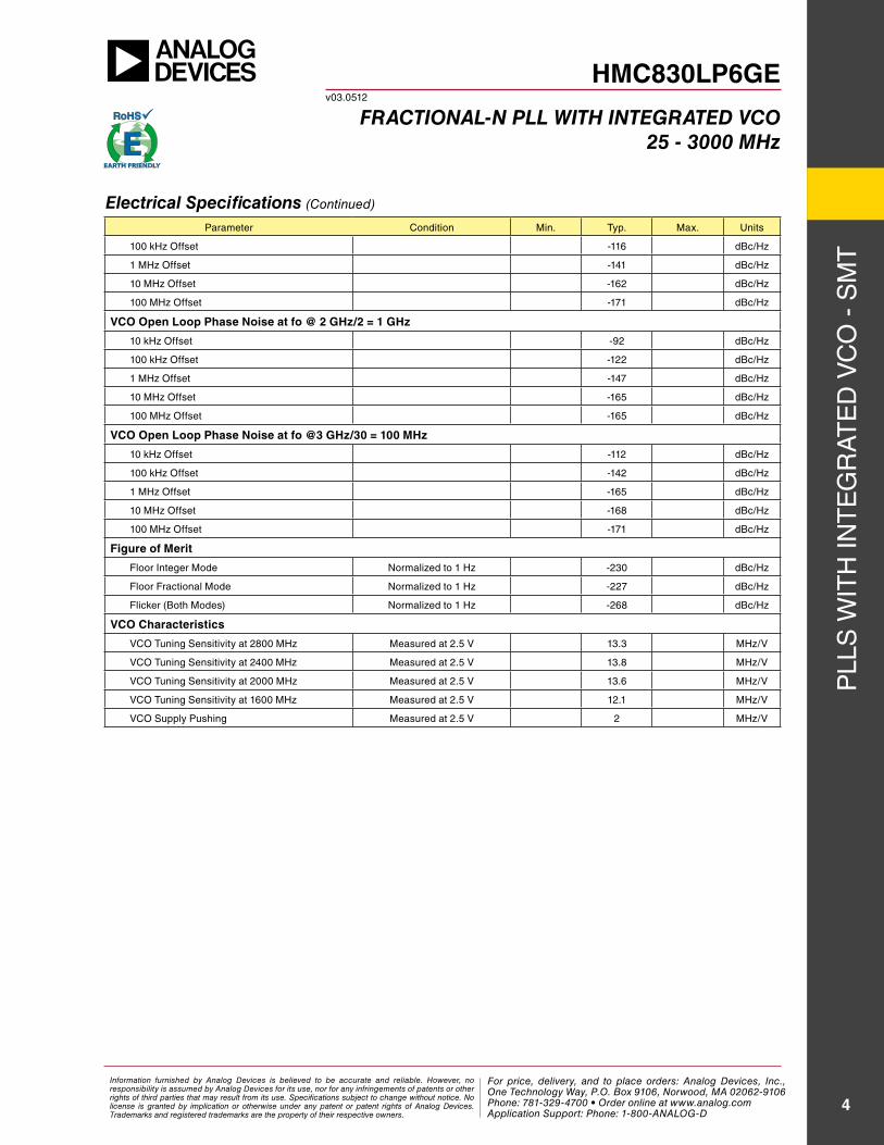
Parameter Condition Min. typ. Max. Units
RF Output Characteristics
Output Frequency 25 3000 Mhz
VCO Frequency at PLL input 1500 3000 Mhz
rF Output Frequency at fVCO 1500 3000 Mhz
Output Power
rF Output Power at fVCO = 2000 Mhz across all Frequencies see Figure 10
Broadband Matched internally [1]
4.5 6 7.5 dBm
Output Power Control 3 dB steps 7 9 dB
Harmonics
fo Mode at 2 ghz 2nd / 3rd / 4th -20/-29/-45 dBc
fo/2 Mode at 2ghz/2 = 1 ghz 2nd / 3rd / 4th -23/-15/-35 dBc
fo/30 Mode at 3 ghz/30 = 100 Mhz 2nd / 3rd / 4th -25/-10/-33 dBc
fo/62 Mode at 1550 Mhz/62 = 25 Mhz 2nd / 3rd / 4th -17/-8/-21 dBc
VCO Output Divider
VCO rF divider range 1,2,4,6,8,...,62 1 62
PLL RF Divider Characteristics
19-Bit n-divider range (integer) Max = 219 - 1 16 524,287
19-Bit n-divider range (Fractional)Fractional nominal divide ratio
varies (-3 / +4) dynamically max20 524,283
REF Input Characteristics
Max ref input Frequency 350 Mhz
ref input VoltageaC Coupled
[2]1 2 3.3 Vp-p
ref input Capacitance 5 pF
electrical SpecificationsVPPcP, VddlS, Vcc1, Vcc2 = 5 V; rVdd, aVdd, dVdd3V, VccPd, VcchF, VccPS = 3.3 V Min and Max Specified across temp -40 °c to 85 °c
[1] Measured single-ended. additional 3 dB possible with differential outputs.[2] Measured with 100 Ω external termination. see hittite PLL w/ integraged VCOs Operating guide reference input stage section for more details.
Information furnished by Analog Devices is believed to be accurate and reliable. However, no responsibility is assumed by Analog Devices for its use, nor for any infringements of patents or other rights of third parties that may result from its use. Specifications subject to change without notice. No license is granted by implication or otherwise under any patent or patent rights of Analog Devices. Trademarks and registered trademarks are the property of their respective owners.
For price, delivery, and to place orders: Analog Devices, Inc., One Technology Way, P.O. Box 9106, Norwood, MA 02062-9106 Phone: 781-329-4700 • Order online at www.analog.com Application Support: Phone: 1-800-ANALOG-D
For price, delivery and to place orders: Hittite Microwave Corporation, 2 Elizabeth Drive, Chelmsford, MA 01824Phone: 978-250-3343 Fax: 978-250-3373 Order On-line at www.hittite.com
Application Support: Phone: 978-250-3343 or [email protected]
PLL
s w
ith
int
eg
rat
ed
VC
O -
sM
t
3
HMC830LP6GEv03.0512
Fractional-n Pll with integrated Vco25 - 3000 Mhz
Parameter Condition Min. typ. Max. Units
14-Bit r-divider range 1 16,383
Phase Detector (PD) [3]
Pd Frequency Fractional Mode B [4] dC 100 Mhz
Pd Frequency Fractional Mode a (and register 6 [17:16] = 11)
dC 80 Mhz
Pd Frequency integer Mode dC 125 Mhz
Charge Pump
Output Current 0.02 2.54 ma
Charge Pump gain step size 20 µa
Pd/Charge Pump ssB Phase noise 50 Mhz ref, input referred
1 khz -143 dBc/hz
10 khz add 1 dB for Fractional -150 dBc/hz
100 khz add 3 dB for Fractional -153 dBc/hz
Logic Inputs
Vsw 40 50 60 % dVdd
Logic Outputs
VOh Output high Voltage dVdd V
VOL Output Low Voltage 0 V
Output impedance 100 200 Ω
Maximum Load Current 1.5 ma
Power Supply Voltages
3.3 V suppliesaVdd, VCChF, VCCPs,VCCPd, rVdd,dVdd
3.0 3.3 3.5 V
5 V supplies VPPCP, VddLs, VCC1, VCC2 4.8 5 5.2 V
Power Supply Currents
+5V analog Charge Pump VPPCP, VddLs 8 ma
+5V VCO Core and VCO Bufferfo/1 Mode VCC2 105 ma
fo/n Mode VCC2 80 ma
+5V VCO divider and rF/PLL Bufferfo/1 Mode VCC1 25 ma
fo/n Mode VCC1 80 100 ma
+3.3VaVdd, VCChF, VCCPs, VCCPd, rVdd, dVdd3V
52 ma
Power down - Crystal Offreg 01h=0,
Crystal not Clocked10 µa
Power down - Crystal On, 100 Mhzreg 01h=0,
Crystal Clocked 100 Mhz10 30 ma
Power on Reset
typical reset Voltage on dVdd 700 mV
Min dVdd Voltage for no reset 1.5 V
Power on reset delay 250 µs
VCO Open Loop Phase Noise at fo @ 2 GHz
10 khz Offset -86 dBc/hz
electrical Specifications (Continued)
[3] slew rate of greater or equal to 0.5 ns/V is recommended, see PLL with integrated rF VCOs Operating guide for more details. Frequency is guaranteed across process voltage and temperature from -40 °C to 85 °C.[4] this maximum phase detector frequency can only be achieved if the minimum n value is respected. eg. in the case of fractional feedback mode, the maximum PFd rate = fvco/20 or 100 Mhz, whichever is less.
Information furnished by Analog Devices is believed to be accurate and reliable. However, no responsibility is assumed by Analog Devices for its use, nor for any infringements of patents or other rights of third parties that may result from its use. Specifications subject to change without notice. No license is granted by implication or otherwise under any patent or patent rights of Analog Devices. Trademarks and registered trademarks are the property of their respective owners.
For price, delivery, and to place orders: Analog Devices, Inc., One Technology Way, P.O. Box 9106, Norwood, MA 02062-9106 Phone: 781-329-4700 • Order online at www.analog.com Application Support: Phone: 1-800-ANALOG-D
For price, delivery and to place orders: Hittite Microwave Corporation, 2 Elizabeth Drive, Chelmsford, MA 01824Phone: 978-250-3343 Fax: 978-250-3373 Order On-line at www.hittite.com
Application Support: Phone: 978-250-3343 or [email protected]
PLL
s w
ith
int
eg
rat
ed
VC
O -
sM
t
4
HMC830LP6GEv03.0512
Fractional-n Pll with integrated Vco25 - 3000 Mhz
electrical Specifications (Continued)
Parameter Condition Min. typ. Max. Units
100 khz Offset -116 dBc/hz
1 Mhz Offset -141 dBc/hz
10 Mhz Offset -162 dBc/hz
100 Mhz Offset -171 dBc/hz
VCO Open Loop Phase Noise at fo @ 2 GHz/2 = 1 GHz
10 khz Offset -92 dBc/hz
100 khz Offset -122 dBc/hz
1 Mhz Offset -147 dBc/hz
10 Mhz Offset -165 dBc/hz
100 Mhz Offset -165 dBc/hz
VCO Open Loop Phase Noise at fo @3 GHz/30 = 100 MHz
10 khz Offset -112 dBc/hz
100 khz Offset -142 dBc/hz
1 Mhz Offset -165 dBc/hz
10 Mhz Offset -168 dBc/hz
100 Mhz Offset -171 dBc/hz
Figure of Merit
Floor integer Mode normalized to 1 hz -230 dBc/hz
Floor Fractional Mode normalized to 1 hz -227 dBc/hz
Flicker (Both Modes) normalized to 1 hz -268 dBc/hz
VCO Characteristics
VCO tuning sensitivity at 2800 Mhz Measured at 2.5 V 13.3 Mhz/V
VCO tuning sensitivity at 2400 Mhz Measured at 2.5 V 13.8 Mhz/V
VCO tuning sensitivity at 2000 Mhz Measured at 2.5 V 13.6 Mhz/V
VCO tuning sensitivity at 1600 Mhz Measured at 2.5 V 12.1 Mhz/V
VCO supply Pushing Measured at 2.5 V 2 Mhz/V
Information furnished by Analog Devices is believed to be accurate and reliable. However, no responsibility is assumed by Analog Devices for its use, nor for any infringements of patents or other rights of third parties that may result from its use. Specifications subject to change without notice. No license is granted by implication or otherwise under any patent or patent rights of Analog Devices. Trademarks and registered trademarks are the property of their respective owners.
For price, delivery, and to place orders: Analog Devices, Inc., One Technology Way, P.O. Box 9106, Norwood, MA 02062-9106 Phone: 781-329-4700 • Order online at www.analog.com Application Support: Phone: 1-800-ANALOG-D
For price, delivery and to place orders: Hittite Microwave Corporation, 2 Elizabeth Drive, Chelmsford, MA 01824Phone: 978-250-3343 Fax: 978-250-3373 Order On-line at www.hittite.com
Application Support: Phone: 978-250-3343 or [email protected]
PLL
s w
ith
int
eg
rat
ed
VC
O -
sM
t
5
HMC830LP6GEv03.0512
Fractional-n Pll with integrated Vco25 - 3000 Mhz
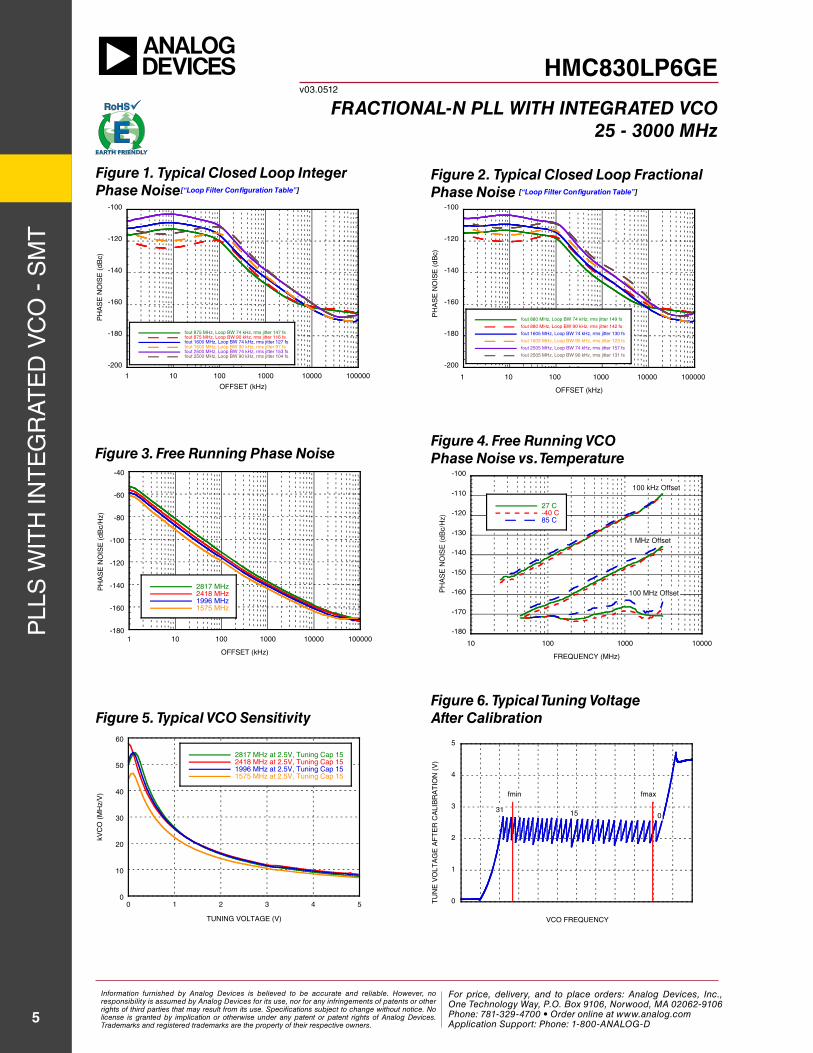
Figure 1. typical closed loop integer Phase noise[“loop Filter configuration table”]
Figure 5. typical Vco Sensitivity
-200
-180
-160
-140
-120
-100
1 10 100 1000 10000 100000
fout 875 MHz, Loop BW 74 kHz, rms jitter 147 fsfout 875 MHz, Loop BW 90 kHz, rms jitter 116 fsfout 1600 MHz, Loop BW 74 kHz, rms jitter 127 fsfout 1600 MHz, Loop BW 90 kHz, rms jitter 97 fsfout 2500 MHz, Loop BW 74 kHz, rms jitter 153 fsfout 2500 MHz, Loop BW 90 kHz, rms jitter 104 fs
OFFSET (kHz)
PH
AS
E N
OIS
E (
dB
c)
-180
-160
-140
-120
-100
-80
-60
-40
1 10 100 1000 10000 100000
2817 MHz2418 MHz1996 MHz1575 MHz
OFFSET (kHz)
PH
AS
E N
OIS
E (
dB
c/H
z)
-180
-170
-160
-150
-140
-130
-120
-110
-100
10 100 1000 10000
27 C-40 C85 C
PH
AS
E N
OIS
E (
dB
c/H
z)
FREQUENCY (MHz)
100 MHz Offset
1 MHz Offset
100 kHz Offset
Figure 2. typical closed loop Fractional Phase noise [“loop Filter configuration table”]
Figure 3. Free running Phase noiseFigure 4. Free running Vco Phase noise vs. temperature
0
1
2
3
4
5
VCO FREQUENCY
TU
NE
VO
LT
AG
E A
FT
ER
CA
LIB
RA
TIO
N (
V)
01531
fmin fmax
-200
-180
-160
-140
-120
-100
1 10 100 1000 10000 100000
fout 880 MHz, Loop BW 74 kHz, rms jitter 149 fs
fout 880 MHz, Loop BW 90 kHz, rms jitter 142 fs
fout 1605 MHz, Loop BW 74 kHz, rms jitter 130 fs
fout 1605 MHz, Loop BW 90 kHz, rms jitter 123 fs
fout 2505 MHz, Loop BW 74 kHz, rms jitter 157 fs
fout 2505 MHz, Loop BW 90 kHz, rms jitter 131 fs
OFFSET (kHz)
PH
AS
E N
OIS
E (
dB
c)
0
10
20
30
40
50
60
0 1 2 3 4 5
2817 MHz at 2.5V, Tuning Cap 152418 MHz at 2.5V, Tuning Cap 151996 MHz at 2.5V, Tuning Cap 151575 MHz at 2.5V, Tuning Cap 15
TUNING VOLTAGE (V)
kV
CO
(M
Hz/V
)
Figure 6. typical tuning Voltage after calibration
Information furnished by Analog Devices is believed to be accurate and reliable. However, no responsibility is assumed by Analog Devices for its use, nor for any infringements of patents or other rights of third parties that may result from its use. Specifications subject to change without notice. No license is granted by implication or otherwise under any patent or patent rights of Analog Devices. Trademarks and registered trademarks are the property of their respective owners.
For price, delivery, and to place orders: Analog Devices, Inc., One Technology Way, P.O. Box 9106, Norwood, MA 02062-9106 Phone: 781-329-4700 • Order online at www.analog.com Application Support: Phone: 1-800-ANALOG-D
For price, delivery and to place orders: Hittite Microwave Corporation, 2 Elizabeth Drive, Chelmsford, MA 01824Phone: 978-250-3343 Fax: 978-250-3373 Order On-line at www.hittite.com
Application Support: Phone: 978-250-3343 or [email protected]
PLL
s w
ith
int
eg
rat
ed
VC
O -
sM
t
6
HMC830LP6GEv03.0512
Fractional-n Pll with integrated Vco25 - 3000 Mhz
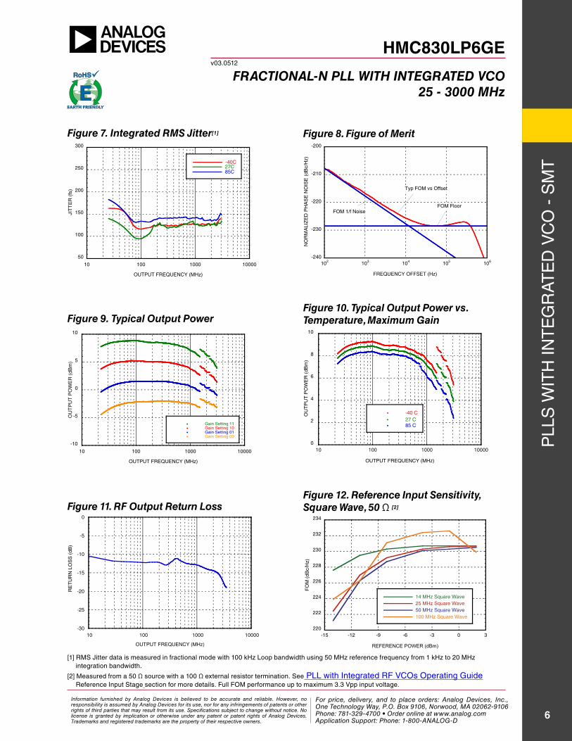
Figure 7. integrated rMS Jitter[1]
[1] rMs Jitter data is measured in fractional mode with 100 khz Loop bandwidth using 50 Mhz reference frequency from 1 khz to 20 Mhz integration bandwidth.
[2] Measured from a 50 Ω source with a 100 Ω external resistor termination. see PLL with integrated rF VCOs Operating guide reference input stage section for more details. Full FOM performance up to maximum 3.3 Vpp input voltage.
50
100
150
200
250
300
10 100 1000 10000
-40C27C85C
JIT
TE
R (
fs)
OUTPUT FREQUENCY (MHz)
-10
-5
0
5
10
10 100 1000 10000
Gain Setting 11Gain Setting 10Gain Setting 01Gain Setting 00
OU
TP
UT
PO
WE
R (
dB
m)
OUTPUT FREQUENCY (MHz)
-240
-230
-220
-210
-200
102
103
104
105
106
NO
RM
AL
IZE
D P
HA
SE
NO
ISE
(d
Bc/H
z)
FREQUENCY OFFSET (Hz)
FOM FloorFOM 1/f Noise
Typ FOM vs Offset
Figure 8. Figure of Merit
Figure 9. typical output PowerFigure 10. typical output Power vs. temperature, Maximum gain
-30
-25
-20
-15
-10
-5
0
10 100 1000 10000
OUTPUT FREQUENCY (MHz)
RE
TU
RN
LO
SS
(d
B)
Figure 11. rF output return loss
220
222
224
226
228
230
232
234
-15 -12 -9 -6 -3 0 3
14 MHz Square Wave
25 MHz Square Wave
50 MHz Square Wave
100 MHz Square Wave
FO
M (
dB
c/H
z)
REFERENCE POWER (dBm)
Figure 12. reference input Sensitivity, Square wave, 50 Ω [2]
0
2
4
6
8
10
10 100 1000 10000
27 C
-40 C
85 C
OU
TP
UT
PO
WE
R (
dB
m)
OUTPUT FREQUENCY (MHz)
Information furnished by Analog Devices is believed to be accurate and reliable. However, no responsibility is assumed by Analog Devices for its use, nor for any infringements of patents or other rights of third parties that may result from its use. Specifications subject to change without notice. No license is granted by implication or otherwise under any patent or patent rights of Analog Devices. Trademarks and registered trademarks are the property of their respective owners.
For price, delivery, and to place orders: Analog Devices, Inc., One Technology Way, P.O. Box 9106, Norwood, MA 02062-9106 Phone: 781-329-4700 • Order online at www.analog.com Application Support: Phone: 1-800-ANALOG-D
For price, delivery and to place orders: Hittite Microwave Corporation, 2 Elizabeth Drive, Chelmsford, MA 01824Phone: 978-250-3343 Fax: 978-250-3373 Order On-line at www.hittite.com
Application Support: Phone: 978-250-3343 or [email protected]
PLL
s w
ith
int
eg
rat
ed
VC
O -
sM
t
7
HMC830LP6GEv03.0512
Fractional-n Pll with integrated Vco25 - 3000 Mhz
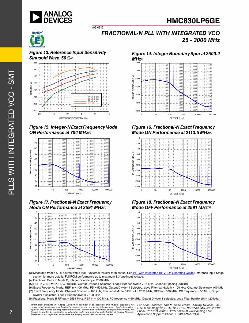
Figure 14. integer Boundary Spur at 2500.2 Mhz[4]
-180
-160
-140
-120
-100
-80
-60
1 10 100 1000 10000 100000
PH
AS
E N
OIS
E (
dB
c/H
z)
OFFSET (kHz)
Figure 13. reference input Sensitivity Sinusoid wave, 50 Ω[3]
200
205
210
215
220
225
230
235
-20 -15 -10 -5 0 5
14 MHz sin25 MHz sin50 MHz sq100 MHz sq
REFERENCE POWER (dBm)
FO
M (
dBc/
Hz)
-180
-160
-140
-120
-100
-80
-60
-40
-20
0
1 10 100 1000 10000 100000
PH
AS
E N
OIS
E (
dB
c/H
z)
OFFSET (kHz)
[3] Measured from a 50 Ω source with a 100 Ω external resistor termination. see PLL with integrated rF VCOs Operating guide reference input stage section for more details. Full FOM performance up to maximum 3.3 Vpp input voltage.
[4] Fractional Mode in Mode B, integer Boundary at 2500 Mhz[5] reF in = 100 Mhz, Pd = 800 khz, Output divider 4 selected, Loop Filter bandwidth = 16 khz, Channel spacing 200 khz[6] exact Frequency Mode, reF in = 100 Mhz, Pd = 50 Mhz, Output divider 1 selected, Loop Filter bandwidth = 100 khz, Channel spacing = 100 khz[7] exact Frequency Mode, Channel spacing = 100 khz, Fractional Mode B rF out = 2591 Mhz, reF in = 100 Mhz, Pd frequency = 50 Mhz, Output
divider 1 selected, Loop Filter bandwidth = 120 khz,[8] Fractional Mode B rF out = 2591 Mhz, reF in = 100 Mhz, Pd frequency = 50 Mhz, Output divider 1 selected, Loop Filter bandwidth = 120 khz.
-180
-160
-140
-120
-100
-80
-60
-40
-20
0
1 10 100 1000 10000 100000
PH
AS
E N
OIS
E (
dB
c/H
z)
OFFSET (kHz)
-180
-160
-140
-120
-100
-80
-60
-40
-20
0
1 10 100 1000 10000 100000
PH
AS
E N
OIS
E (
dB
c/H
z)
OFFSET (kHz)
Figure 15. integer-n exact Frequency Mode on Performance at 704 Mhz[5]
-180
-160
-140
-120
-100
-80
-60
-40
-20
0
1 10 100 1000 10000 100000
PH
AS
E N
OIS
E (
dB
c/H
z)
OFFSET (kHz)
Figure 16. Fractional-n exact Frequency Mode on Performance at 2113.5 Mhz[6]
Figure 17. Fractional-n exact Frequency Mode on Performance at 2591 Mhz[7]
Figure 18. Fractional-n exact Frequency Mode oFF Performance at 2591 Mhz[8]
Information furnished by Analog Devices is believed to be accurate and reliable. However, no responsibility is assumed by Analog Devices for its use, nor for any infringements of patents or other rights of third parties that may result from its use. Specifications subject to change without notice. No license is granted by implication or otherwise under any patent or patent rights of Analog Devices. Trademarks and registered trademarks are the property of their respective owners.
For price, delivery, and to place orders: Analog Devices, Inc., One Technology Way, P.O. Box 9106, Norwood, MA 02062-9106 Phone: 781-329-4700 • Order online at www.analog.com Application Support: Phone: 1-800-ANALOG-D
For price, delivery and to place orders: Hittite Microwave Corporation, 2 Elizabeth Drive, Chelmsford, MA 01824Phone: 978-250-3343 Fax: 978-250-3373 Order On-line at www.hittite.com
Application Support: Phone: 978-250-3343 or [email protected]
PLL
s w
ith
int
eg
rat
ed
VC
O -
sM
t
8
HMC830LP6GEv03.0512
Fractional-n Pll with integrated Vco25 - 3000 Mhz
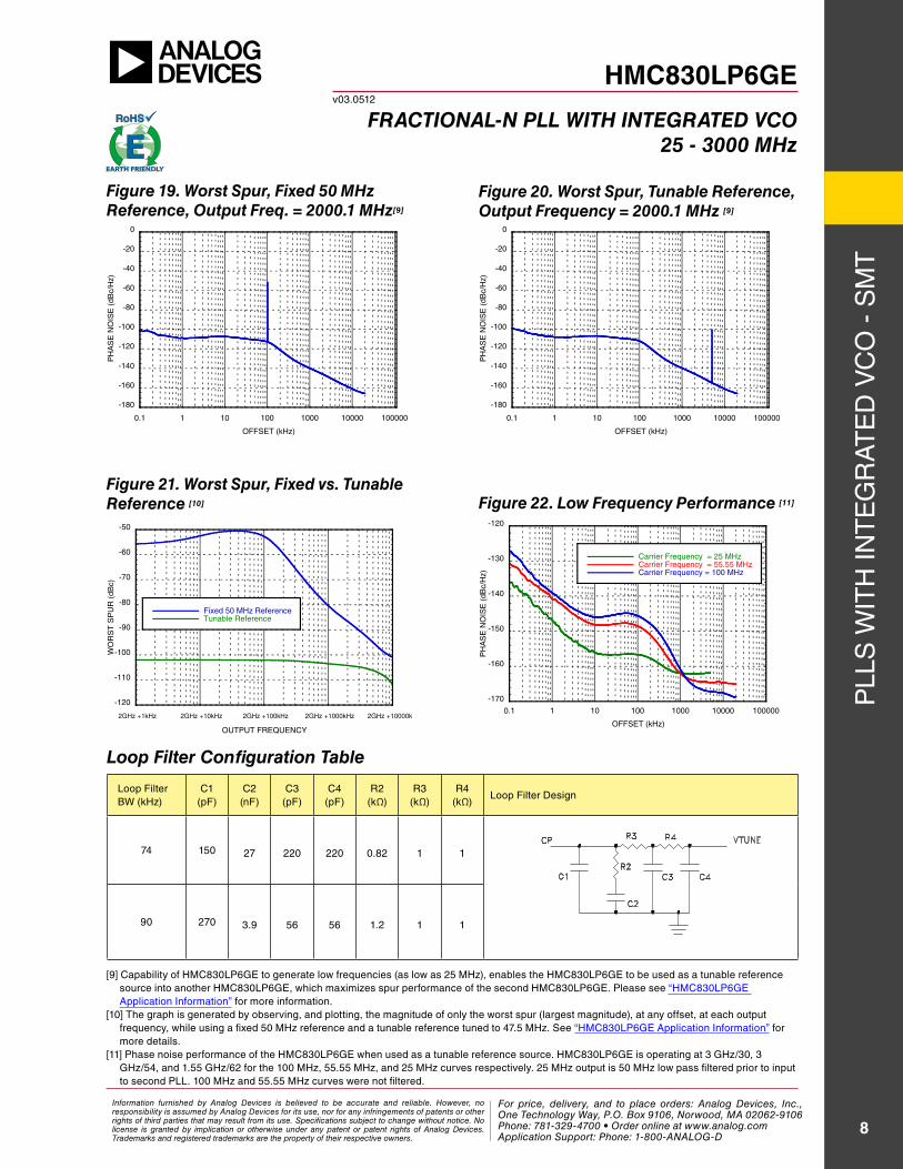
Loop Filter Bw (khz)
C1 (pF)
C2 (nF)
C3 (pF)
C4 (pF)
r2 (kΩ)
r3 (kΩ)
r4 (kΩ)
Loop Filter design
74 150 27 220 220 0.82 1 1
90 270 3.9 56 56 1.2 1 1
loop Filter configuration table
Figure 19. worst Spur, Fixed 50 Mhz reference, output Freq. = 2000.1 Mhz[9]
-180
-160
-140
-120
-100
-80
-60
-40
-20
0
0.1 1 10 100 1000 10000 100000
PH
AS
E N
OIS
E (
dB
c/H
z)
OFFSET (kHz)
Figure 20. worst Spur, tunable reference, output Frequency = 2000.1 Mhz [9]
-180
-160
-140
-120
-100
-80
-60
-40
-20
0
0.1 1 10 100 1000 10000 100000
PH
AS
E N
OIS
E (
dB
c/H
z)
OFFSET (kHz)
Figure 21. worst Spur, Fixed vs. tunable reference [10]
-120
-110
-100
-90
-80
-70
-60
-50
2GHz +1kHz 2GHz +10kHz 2GHz +100kHz 2GHz +1000kHz 2GHz +10000kHz
Fixed 50 MHz ReferenceTunable Reference
WO
RS
T S
PU
R (
dB
c)
OUTPUT FREQUENCY
[9] Capability of hMC830LP6ge to generate low frequencies (as low as 25 Mhz), enables the hMC830LP6ge to be used as a tunable reference source into another hMC830LP6ge, which maximizes spur performance of the second hMC830LP6ge. Please see “hMC830LP6ge application information” for more information.
[10] the graph is generated by observing, and plotting, the magnitude of only the worst spur (largest magnitude), at any offset, at each output frequency, while using a fixed 50 Mhz reference and a tunable reference tuned to 47.5 Mhz. see “hMC830LP6ge application information” for more details.
[11] Phase noise performance of the hMC830LP6ge when used as a tunable reference source. hMC830LP6ge is operating at 3 ghz/30, 3 ghz/54, and 1.55 ghz/62 for the 100 Mhz, 55.55 Mhz, and 25 Mhz curves respectively. 25 Mhz output is 50 Mhz low pass filtered prior to input to second PLL. 100 Mhz and 55.55 Mhz curves were not filtered.
Figure 22. low Frequency Performance [11]
-170
-160
-150
-140
-130
-120
0.1 1 10 100 1000 10000 100000
Carrier Frequency = 25 MHzCarrier Frequency = 55.55 MHzCarrier Frequency = 100 MHz
PH
AS
E N
OIS
E (
dB
c/H
z)
OFFSET (kHz)
Information furnished by Analog Devices is believed to be accurate and reliable. However, no responsibility is assumed by Analog Devices for its use, nor for any infringements of patents or other rights of third parties that may result from its use. Specifications subject to change without notice. No license is granted by implication or otherwise under any patent or patent rights of Analog Devices. Trademarks and registered trademarks are the property of their respective owners.
For price, delivery, and to place orders: Analog Devices, Inc., One Technology Way, P.O. Box 9106, Norwood, MA 02062-9106 Phone: 781-329-4700 • Order online at www.analog.com Application Support: Phone: 1-800-ANALOG-D
For price, delivery and to place orders: Hittite Microwave Corporation, 2 Elizabeth Drive, Chelmsford, MA 01824Phone: 978-250-3343 Fax: 978-250-3373 Order On-line at www.hittite.com
Application Support: Phone: 978-250-3343 or [email protected]
PLL
s w
ith
int
eg
rat
ed
VC
O -
sM
t
9
HMC830LP6GEv03.0512
Fractional-n Pll with integrated Vco25 - 3000 Mhz
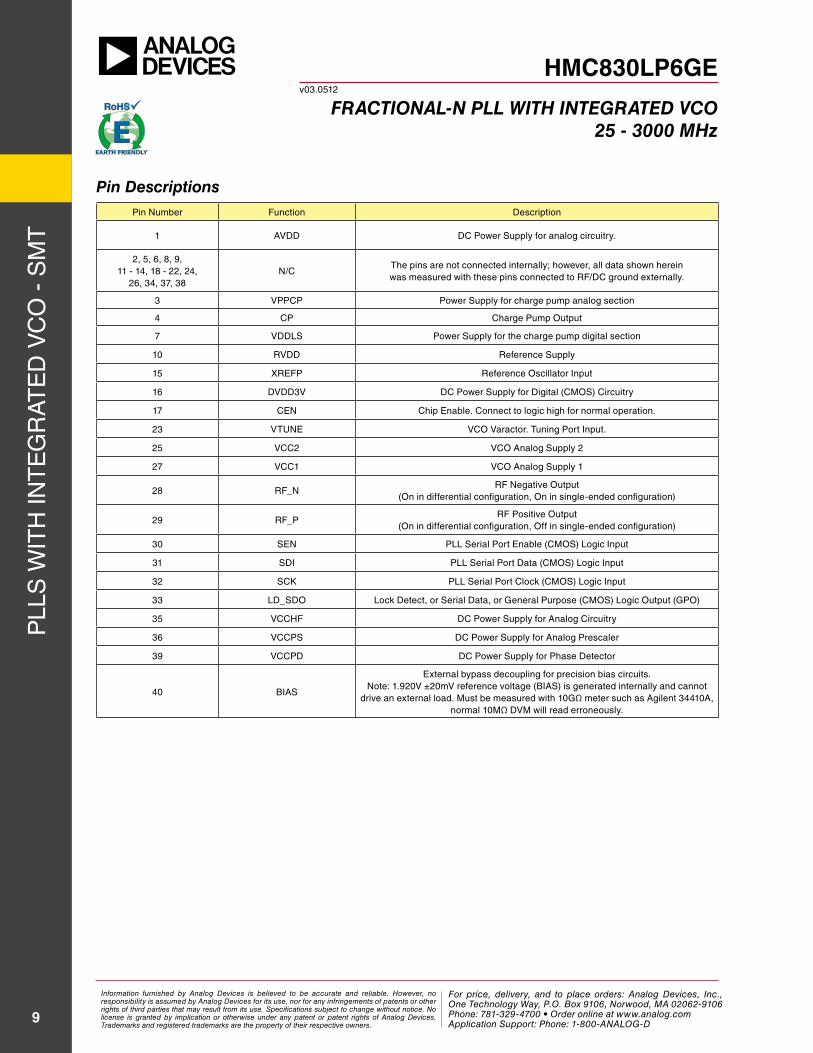
Pin descriptionsPin number Function description
1 aVdd dC Power supply for analog circuitry.
2, 5, 6, 8, 9, 11 - 14, 18 - 22, 24,
26, 34, 37, 38n/C
the pins are not connected internally; however, all data shown herein was measured with these pins connected to rF/dC ground externally.
3 VPPCP Power supply for charge pump analog section
4 CP Charge Pump Output
7 VddLs Power supply for the charge pump digital section
10 rVdd reference supply
15 XreFP reference Oscillator input
16 dVdd3V dC Power supply for digital (CMOs) Circuitry
17 Cen Chip enable. Connect to logic high for normal operation.
23 VtUne VCO Varactor. tuning Port input.
25 VCC2 VCO analog supply 2
27 VCC1 VCO analog supply 1
28 rF_nrF negative Output
(On in differential configuration, On in single-ended configuration)
29 rF_PrF Positive Output
(On in differential configuration, Off in single-ended configuration)
30 sen PLL serial Port enable (CMOs) Logic input
31 sdi PLL serial Port data (CMOs) Logic input
32 sCK PLL serial Port Clock (CMOs) Logic input
33 Ld_sdO Lock detect, or serial data, or general Purpose (CMOs) Logic Output (gPO)
35 VCChF dC Power supply for analog Circuitry
36 VCCPs dC Power supply for analog Prescaler
39 VCCPd dC Power supply for Phase detector
40 Bias
external bypass decoupling for precision bias circuits. note: 1.920V ±20mV reference voltage (Bias) is generated internally and cannot
drive an external load. Must be measured with 10gΩ meter such as agilent 34410a, normal 10MΩ dVM will read erroneously.
Information furnished by Analog Devices is believed to be accurate and reliable. However, no responsibility is assumed by Analog Devices for its use, nor for any infringements of patents or other rights of third parties that may result from its use. Specifications subject to change without notice. No license is granted by implication or otherwise under any patent or patent rights of Analog Devices. Trademarks and registered trademarks are the property of their respective owners.
For price, delivery, and to place orders: Analog Devices, Inc., One Technology Way, P.O. Box 9106, Norwood, MA 02062-9106 Phone: 781-329-4700 • Order online at www.analog.com Application Support: Phone: 1-800-ANALOG-D
For price, delivery and to place orders: Hittite Microwave Corporation, 2 Elizabeth Drive, Chelmsford, MA 01824Phone: 978-250-3343 Fax: 978-250-3373 Order On-line at www.hittite.com
Application Support: Phone: 978-250-3343 or [email protected]
PLL
s w
ith
int
eg
rat
ed
VC
O -
sM
t
10
HMC830LP6GEv03.0512
Fractional-n Pll with integrated Vco25 - 3000 Mhz
absolute Maximum ratingsaVdd, rVdd, dVdd3V, VCCPd, VCChF, VCCPs
-0.3 V to +3.6 V
VPPCP, VddLs, VCC1 -0.3 V to +5.5 V
VCC2 -0.3 V to +5.5 V
Operating temperature -40 °C to +85 °C
storage temperature -65 °C to 150 °C
Maximum Junction temperature 150 °C
thermal resistance (ѲJC) (junction to case (ground paddle))
9 °C/w
reflow soldering
Peak temperature 260 °C
time at Peak temperature 40 sec
esd sensitivity (hBM) Class 1B
stresses above those listed under absolute Maximum ratings may cause permanent damage to the device. this is a stress rating only; functional operation of the device at these or any other conditions above those indicated in the operational section of this specification is not implied. exposure to absolute maximum rating conditions for extended periods may affect device reliability.
recommended operating conditionsParameter Condition Min. typ. Max. Units
Temperature
Junction temperature 125 °C
ambient temperature -40 85 °C
Supply Voltage
aVdd, rVdd, dVdd3V, VCCPd, VCChF, VCCPs
3.0 3.3 3.5 V
VPPCP, VddLs, VCC1, VCC2 4.8 5 5.2 V
[1] Layout design guidelines set out in Qualification test report are strongly recommended.
Information furnished by Analog Devices is believed to be accurate and reliable. However, no responsibility is assumed by Analog Devices for its use, nor for any infringements of patents or other rights of third parties that may result from its use. Specifications subject to change without notice. No license is granted by implication or otherwise under any patent or patent rights of Analog Devices. Trademarks and registered trademarks are the property of their respective owners.
For price, delivery, and to place orders: Analog Devices, Inc., One Technology Way, P.O. Box 9106, Norwood, MA 02062-9106 Phone: 781-329-4700 • Order online at www.analog.com Application Support: Phone: 1-800-ANALOG-D
For price, delivery and to place orders: Hittite Microwave Corporation, 2 Elizabeth Drive, Chelmsford, MA 01824Phone: 978-250-3343 Fax: 978-250-3373 Order On-line at www.hittite.com
Application Support: Phone: 978-250-3343 or [email protected]
PLL
s w
ith
int
eg
rat
ed
VC
O -
sM
t
11
HMC830LP6GEv03.0512
Fractional-n Pll with integrated Vco25 - 3000 Mhz
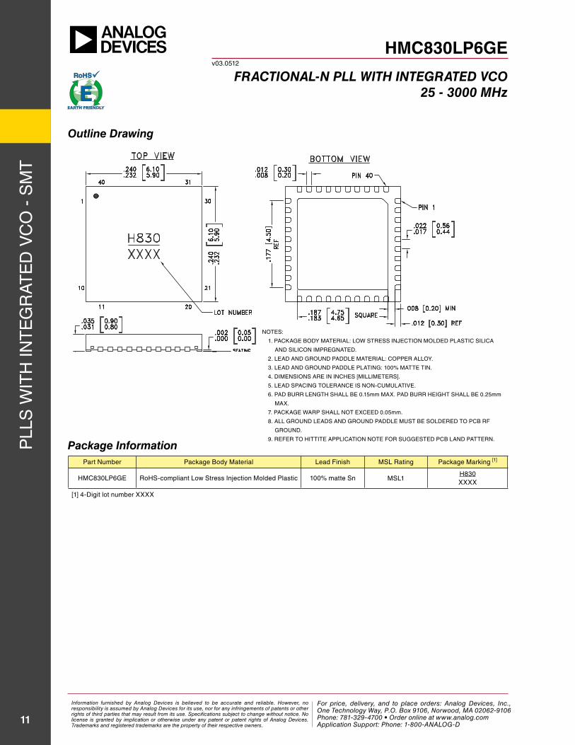
outline drawing
Part number Package Body Material Lead Finish MsL rating Package Marking [1]
hMC830LP6ge rohs-compliant Low stress injection Molded Plastic 100% matte sn MsL1h830XXXX
[1] 4-digit lot number XXXX
Package information
nOtes:
1. PaCKage BOdY MateriaL: LOw stress inJeCtiOn MOLded PLastiC siLiCa
and siLiCOn iMPregnated.
2. Lead and grOUnd PaddLe MateriaL: COPPer aLLOY.
3. Lead and grOUnd PaddLe PLating: 100% Matte tin.
4. diMensiOns are in inChes [MiLLiMeters].
5. Lead sPaCing tOLeranCe is nOn-CUMULatiVe.
6. Pad BUrr Length shaLL Be 0.15mm MaX. Pad BUrr height shaLL Be 0.25mm
MaX.
7. PaCKage warP shaLL nOt eXCeed 0.05mm.
8. aLL grOUnd Leads and grOUnd PaddLe MUst Be sOLdered tO PCB rF
grOUnd.
9. reFer tO hittite aPPLiCatiOn nOte FOr sUggested PCB Land Pattern.
Information furnished by Analog Devices is believed to be accurate and reliable. However, no responsibility is assumed by Analog Devices for its use, nor for any infringements of patents or other rights of third parties that may result from its use. Specifications subject to change without notice. No license is granted by implication or otherwise under any patent or patent rights of Analog Devices. Trademarks and registered trademarks are the property of their respective owners.
For price, delivery, and to place orders: Analog Devices, Inc., One Technology Way, P.O. Box 9106, Norwood, MA 02062-9106 Phone: 781-329-4700 • Order online at www.analog.com Application Support: Phone: 1-800-ANALOG-D
For price, delivery and to place orders: Hittite Microwave Corporation, 2 Elizabeth Drive, Chelmsford, MA 01824Phone: 978-250-3343 Fax: 978-250-3373 Order On-line at www.hittite.com
Application Support: Phone: 978-250-3343 or [email protected]
PLL
s w
ith
int
eg
rat
ed
VC
O -
sM
t
12
HMC830LP6GEv03.0512
Fractional-n Pll with integrated Vco25 - 3000 Mhz
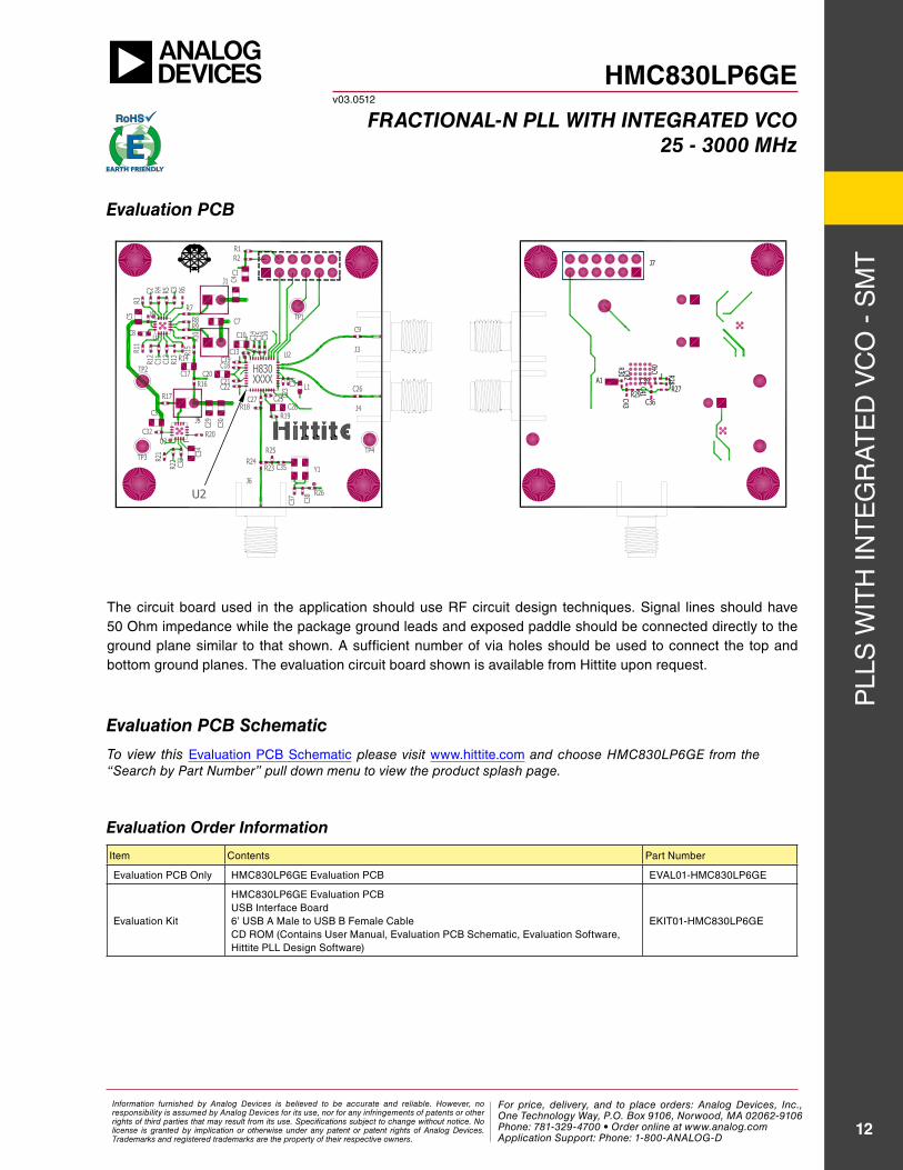
evaluation PcB Schematic
the circuit board used in the application should use rF circuit design techniques. signal lines should have 50 Ohm impedance while the package ground leads and exposed paddle should be connected directly to the ground plane similar to that shown. a sufficient number of via holes should be used to connect the top and bottom ground planes. the evaluation circuit board shown is available from hittite upon request.
To view this evaluation PCB schematic please visit www.hittite.com and choose HMC830LP6GE from the “Search by Part Number” pull down menu to view the product splash page.
evaluation PcB
item Contents Part number
evaluation PCB Only hMC830LP6ge evaluation PCB eVaL01-hMC830LP6ge
evaluation Kit
hMC830LP6ge evaluation PCBUsB interface Board6’ UsB a Male to UsB B Female CableCd rOM (Contains User Manual, evaluation PCB schematic, evaluation software, hittite PLL design software)
eKit01-hMC830LP6ge
evaluation order information
Information furnished by Analog Devices is believed to be accurate and reliable. However, no responsibility is assumed by Analog Devices for its use, nor for any infringements of patents or other rights of third parties that may result from its use. Specifications subject to change without notice. No license is granted by implication or otherwise under any patent or patent rights of Analog Devices. Trademarks and registered trademarks are the property of their respective owners.
For price, delivery, and to place orders: Analog Devices, Inc., One Technology Way, P.O. Box 9106, Norwood, MA 02062-9106 Phone: 781-329-4700 • Order online at www.analog.com Application Support: Phone: 1-800-ANALOG-D
For price, delivery and to place orders: Hittite Microwave Corporation, 2 Elizabeth Drive, Chelmsford, MA 01824Phone: 978-250-3343 Fax: 978-250-3373 Order On-line at www.hittite.com
Application Support: Phone: 978-250-3343 or [email protected]
PLL
s w
ith
int
eg
rat
ed
VC
O -
sM
t
13
HMC830LP6GEv03.0512
Fractional-n Pll with integrated Vco25 - 3000 Mhz
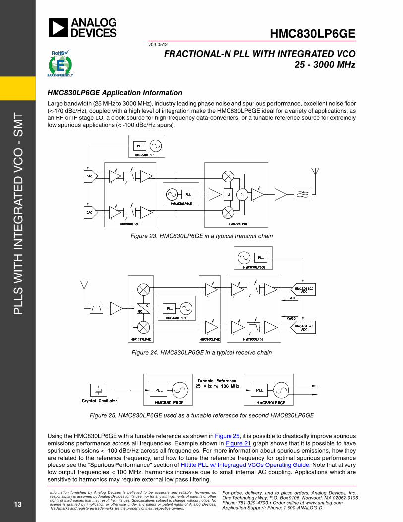
hMc830lP6ge application informationLarge bandwidth (25 Mhz to 3000 Mhz), industry leading phase noise and spurious performance, excellent noise floor (<-170 dBc/hz), coupled with a high level of integration make the hMC830LP6ge ideal for a variety of applications; as an rF or iF stage LO, a clock source for high-frequency data-converters, or a tunable reference source for extremely low spurious applications (< -100 dBc/hz spurs).
Figure 23. HMC830LP6GE in a typical transmit chain
Figure 24. HMC830LP6GE in a typical receive chain
Figure 25. HMC830LP6GE used as a tunable reference for second HMC830LP6GE
Using the hMC830LP6ge with a tunable reference as shown in Figure 25, it is possible to drastically improve spurious emissions performance across all frequencies. example shown in Figure 21 graph shows that it is possible to have spurious emissions < -100 dBc/hz across all frequencies. For more information about spurious emissions, how they are related to the reference frequency, and how to tune the reference frequency for optimal spurious performance please see the “spurious Performance” section of hittite PLL w/ integraged VCOs Operating guide. note that at very low output frequencies < 100 Mhz, harmonics increase due to small internal aC coupling. applications which are sensitive to harmonics may require external low pass filtering.
Information furnished by Analog Devices is believed to be accurate and reliable. However, no responsibility is assumed by Analog Devices for its use, nor for any infringements of patents or other rights of third parties that may result from its use. Specifications subject to change without notice. No license is granted by implication or otherwise under any patent or patent rights of Analog Devices. Trademarks and registered trademarks are the property of their respective owners.
For price, delivery, and to place orders: Analog Devices, Inc., One Technology Way, P.O. Box 9106, Norwood, MA 02062-9106 Phone: 781-329-4700 • Order online at www.analog.com Application Support: Phone: 1-800-ANALOG-D
For price, delivery and to place orders: Hittite Microwave Corporation, 2 Elizabeth Drive, Chelmsford, MA 01824Phone: 978-250-3343 Fax: 978-250-3373 Order On-line at www.hittite.com
Application Support: Phone: 978-250-3343 or [email protected]
PLL
s w
ith
int
eg
rat
ed
VC
O -
sM
t
14
HMC830LP6GEv03.0512
Fractional-n Pll with integrated Vco25 - 3000 Mhz
notes:
Information furnished by Analog Devices is believed to be accurate and reliable. However, no responsibility is assumed by Analog Devices for its use, nor for any infringements of patents or other rights of third parties that may result from its use. Specifications subject to change without notice. No license is granted by implication or otherwise under any patent or patent rights of Analog Devices. Trademarks and registered trademarks are the property of their respective owners.
For price, delivery, and to place orders: Analog Devices, Inc., One Technology Way, P.O. Box 9106, Norwood, MA 02062-9106 Phone: 781-329-4700 • Order online at www.analog.com Application Support: Phone: 1-800-ANALOG-D
Recommended