Getting All the Light Out, or No Photon Left Behind
Steve Forrest
Departments of Electrical Engineering and
Computer Science, and Physics
University of Michigan
Ann Arbor, MI 48109
OLEDs: Major Remaining Challenges for Lighting
• Blue Lifetime
• Getting the Light Out
• Cost & Yield
– Patterning & Deposition
– Throughput
Cathode metal (mirror)
Organics
ITO
Glass substrate
k||
k
θ
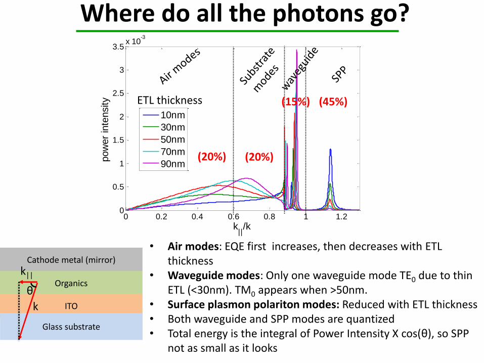
• Air modes: EQE first increases, then decreases with ETL thickness
• Waveguide modes: Only one waveguide mode TE0 due to thin ETL (<30nm). TM0 appears when >50nm.
• Surface plasmon polariton modes: Reduced with ETL thickness • Both waveguide and SPP modes are quantized • Total energy is the integral of Power Intensity X cos(θ), so SPP
not as small as it looks
Where do all the photons go?
0 0.2 0.4 0.6 0.8 1 1.20
0.5
1
1.5
2
2.5
3
3.5x 10
-3
k||/k
pow
er
inte
nsity
10nm
30nm
50nm
70nm
90nm
ETL thickness
(20%) (20%)
(15%) (45%)
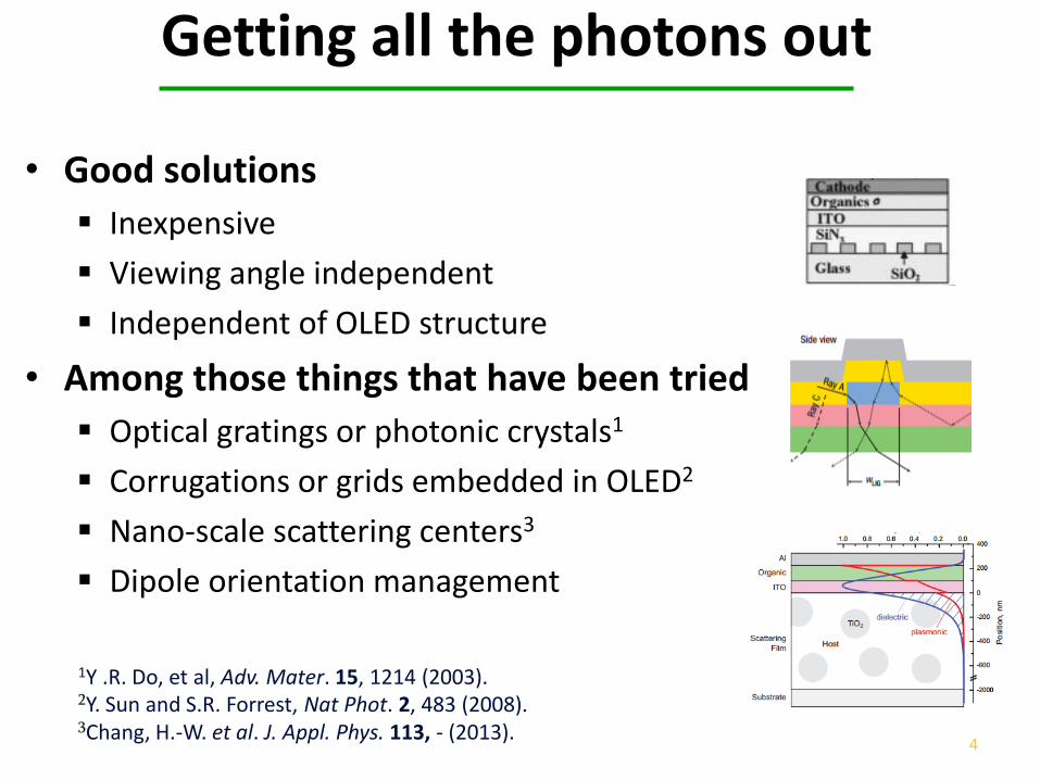
• Good solutions
Inexpensive
Viewing angle independent
Independent of OLED structure
• Among those things that have been tried
Optical gratings or photonic crystals1
Corrugations or grids embedded in OLED2
Nano-scale scattering centers3
Dipole orientation management
4
1Y .R. Do, et al, Adv. Mater. 15, 1214 (2003). 2Y. Sun and S.R. Forrest, Nat Phot. 2, 483 (2008). 3Chang, H.-W. et al. J. Appl. Phys. 113, - (2013).
Getting all the photons out
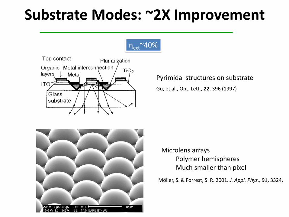
Substrate Modes: ~2X Improvement
Gu, et al., Opt. Lett., 22, 396 (1997)
ηext~40%
Pyrimidal structures on substrate
Microlens arrays Polymer hemispheres Much smaller than pixel
Möller, S. & Forrest, S. R. 2001. J. Appl. Phys., 91, 3324.
6
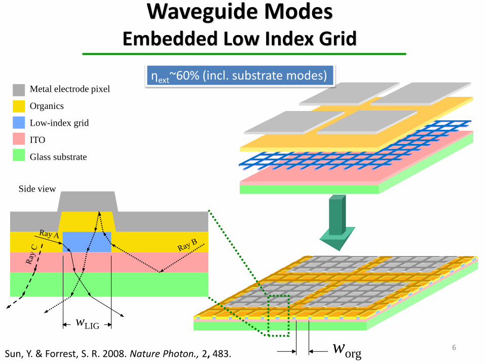
Metal electrode pixel
Organics
Low-index grid
ITO
Glass substrate
Side view
wLIG
worg
Waveguide Modes Embedded Low Index Grid
ηext~60% (incl. substrate modes)
Sun, Y. & Forrest, S. R. 2008. Nature Photon., 2, 483.
7
2mm
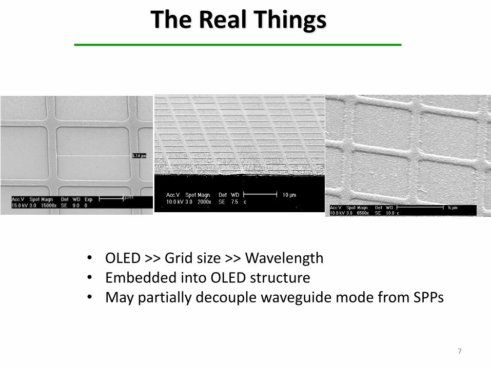
The Real Things
• OLED >> Grid size >> Wavelength • Embedded into OLED structure • May partially decouple waveguide mode from SPPs
8
400 600 800
0.0
0.5
1.0
No
rm.
EL
(a
.u.)
Wavelength (nm)
Dev. 1
Dev. 4
10-6
1x10⁻⁵
1x10⁻⁴
10-3
10-2
10-1
0
10
20
30
Po
we
r E
ffic
ien
cy (
lm/W
)
Exte
rna
l Q
ua
ntu
m E
ffic
ien
cy (
%)
Current Density (mA/cm2)
Dev. 4
Dev. 3
Dev. 2
Dev. 1
0
10
20
30
40
50
60
70
80
Dev. 1 x 1.32
Dev.1x1.68
Dev. 1 x 2.3
10-3 10-2 10-1 100 101 102 10-3 10-2 10-1 100 101 102
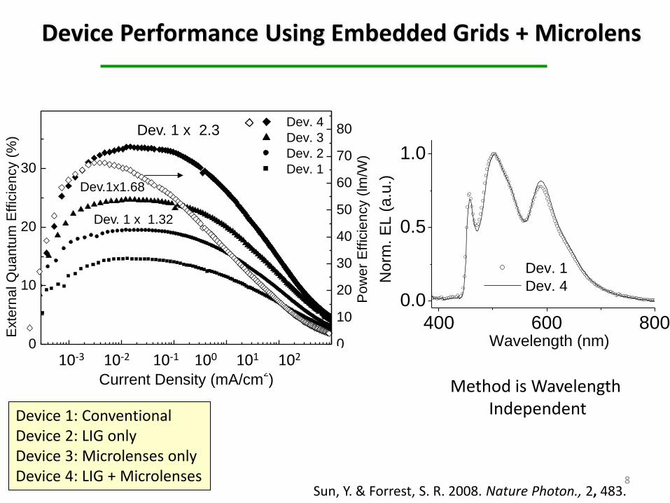
Device Performance Using Embedded Grids + Microlens
Device 1: Conventional Device 2: LIG only Device 3: Microlenses only Device 4: LIG + Microlenses
Method is Wavelength Independent
Sun, Y. & Forrest, S. R. 2008. Nature Photon., 2, 483.
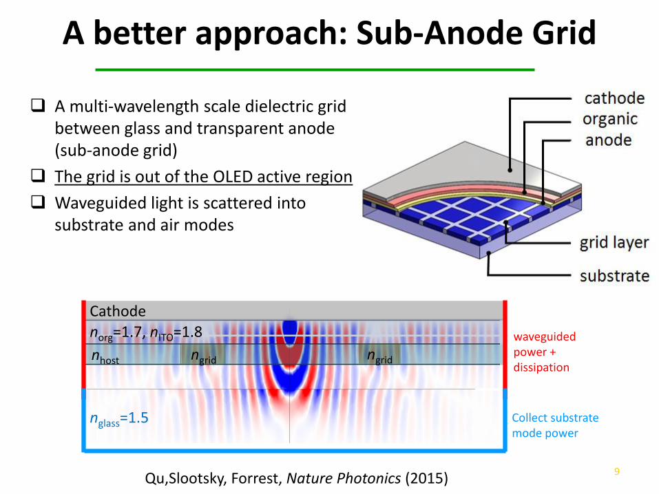
A better approach: Sub-Anode Grid
A multi-wavelength scale dielectric grid between glass and transparent anode (sub-anode grid)
The grid is out of the OLED active region
Waveguided light is scattered into substrate and air modes
9
Cathode
nglass=1.5
nhost
norg=1.7, nITO=1.8
ngrid ngrid waveguided power + dissipation
Collect substrate mode power
Qu,Slootsky, Forrest, Nature Photonics (2015)
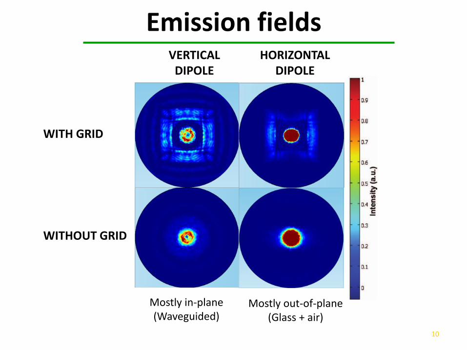
Emission fields
10
WITH GRID
WITHOUT GRID
VERTICAL DIPOLE
HORIZONTAL DIPOLE
Mostly in-plane (Waveguided)
Mostly out-of-plane (Glass + air)
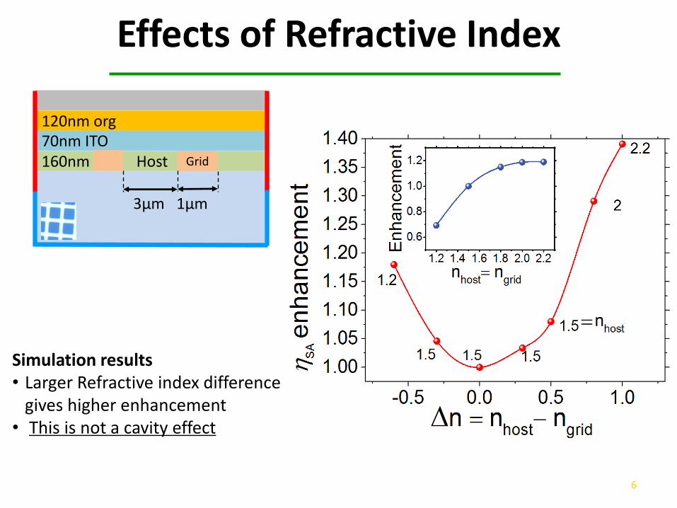
Effects of Refractive Index
6
160nm Host
120nm org 70nm ITO
Grid
3µm 1µm
Simulation results • Larger Refractive index difference
gives higher enhancement • This is not a cavity effect
450 500 550 600 650 700 750 8000.0
0.5
1.0
Inte
nsity (
No
rm.)
Wavelength (nm)
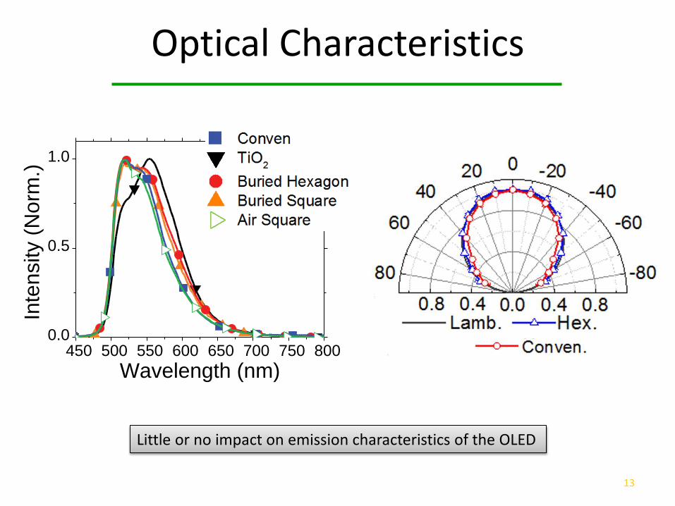
Optical Characteristics
13
Little or no impact on emission characteristics of the OLED
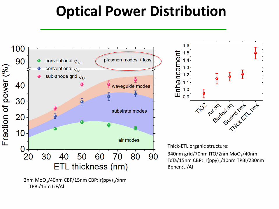
Optical Power Distribution
Thick-ETL organic structure:
340nm grid/70nm ITO/2nm MoO3/40nm TcTa/15nm CBP: Ir(ppy)3/10nm TPBi/230nm Bphen:Li/Al
2nm MoO3/40nm CBP/15nm CBP:Ir(ppy)3/xnm TPBi/1nm LiF/Al
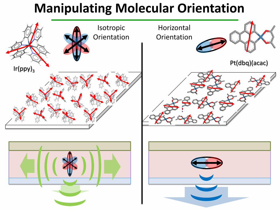
Pt(dbq)(acac)
Isotropic Orientation
Horizontal Orientation
Manipulating Molecular Orientation
Ir(ppy)3
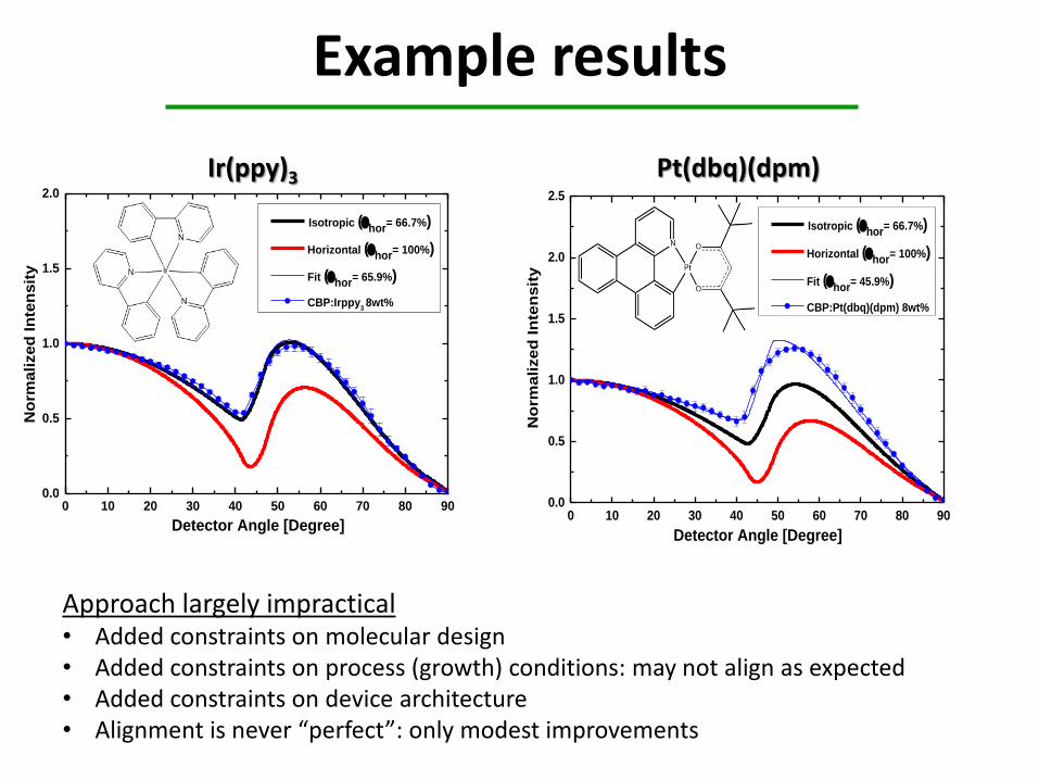
Example results
0 10 20 30 40 50 60 70 80 900.0
0.5
1.0
1.5
2.0
2.5
Detector Angle [Degree]N
orm
alize
d I
nte
nsit
y
Isotropic (hor
= 66.7%)
Horizontal (hor
= 100%)
Fit (hor
= 45.9%)
CBP:Pt(dbq)(dpm) 8wt%
Pt(dbq)(dpm)
0 10 20 30 40 50 60 70 80 900.0
0.5
1.0
1.5
2.0
Detector Angle [Degree]
No
rmalized
In
ten
sit
y
Isotropic (hor
= 66.7%)
Horizontal (hor
= 100%)
Fit (hor
= 65.9%)
CBP:Irppy3 8wt%
Ir(ppy)3
Approach largely impractical • Added constraints on molecular design • Added constraints on process (growth) conditions: may not align as expected • Added constraints on device architecture • Alignment is never “perfect”: only modest improvements
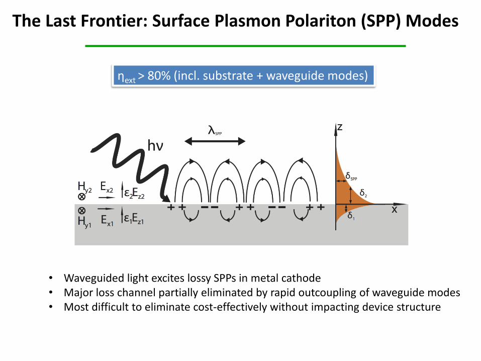
The Last Frontier: Surface Plasmon Polariton (SPP) Modes
ηext > 80% (incl. substrate + waveguide modes)
• Waveguided light excites lossy SPPs in metal cathode • Major loss channel partially eliminated by rapid outcoupling of waveguide modes • Most difficult to eliminate cost-effectively without impacting device structure
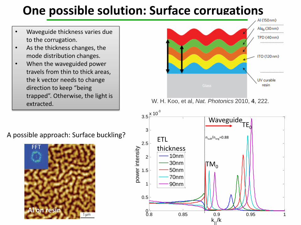
One possible solution: Surface corrugations
• Waveguide thickness varies dueto the corrugation.
• As the thickness changes, themode distribution changes.
• When the waveguided powertravels from thin to thick areas,the k vector needs to changedirection to keep “beingtrapped”. Otherwise, the light isextracted.
0.8 0.85 0.9 0.95 10
0.5
1
1.5
2
2.5
3
3.5x 10
-3
k||/k
pow
er
inte
nsity
10nm
30nm
50nm
70nm
90nm
TM0
TE0
ETL thickness
Waveguide
nsub/norg=0.88
W. H. Koo, et al, Nat. Photonics 2010, 4, 222.
A possible approach: Surface buckling?
FFT
Al on resin

• Simple design that does not interfere with OLED structure • Only substrate processing • Extracts all wavelengths approximately equally • 80-90% extraction within reach!
0 50 100 150
0
10
20
30
40
50
60
70
80
90
100
Power at:
460 nm
510 nm
600 nm
Air modes
Waveguide modes
Fra
cti
on
of
Po
we
r (%
)
ETL Thickness (nm)
Surface plasmon
+ Loss
SubstrateMetalmirror
ITO70nmOrganic120nm
ITO50nm
SiO2xnm
SiO2
How Much Light Can We Realistically Hope to Extract?
Conclusions
• Optimal criteria for outcoupling solutions
– Low cost
– Angle and wavelength independent
– Minimal impact on established OLED and materials designs
• Sub-anode grid outcouples all waveguide modes
• No impact on electrical characteristics
• No significant optical effect
• No active dead zone
• SPP Modes are the final frontier
– 80% outcoupling may be possible if appropriate techniques are employed
20
Recommended