FPGAs, Scaling and Reliability
Douglas SheldonParts Engineering
Jet Propulsion LaboratoryCalifornia Institute of Technology
Copyright 2009 California Institute of TechnologyMay be published with permission by MAPLD 2009
D. Sheldon - MAPLD 2009
Overview
• Introduction• Scaling Overview• Scaling examples:
– Hot Carrier– Negative Bias Temperature Instability – Package– ESD– FPGA Resources– FPGA Costs
Page 2

D. Sheldon - MAPLD 2009
What do we mean by scaling?
9/1/09 Page 3
Chen IBM 2006

D. Sheldon - MAPLD 20099/1/09 Page 4

D. Sheldon - MAPLD 20099/1/09 Page 5

D. Sheldon - MAPLD 20099/1/09 Page 6

D. Sheldon - MAPLD 2009
Static/Passive Power Problem
9/1/09 Page 7
T. N. Theis IBM 2007

D. Sheldon - MAPLD 2009
Fundamental change over to metal gate devices
9/1/09 Page 8
Chen IBM 2006

D. Sheldon - MAPLD 20099/1/09 Page 9

D. Sheldon - MAPLD 20099/1/09 Page 10
D. Sheldon - MAPLD 20099/1/09 Page 11

D. Sheldon - MAPLD 2009
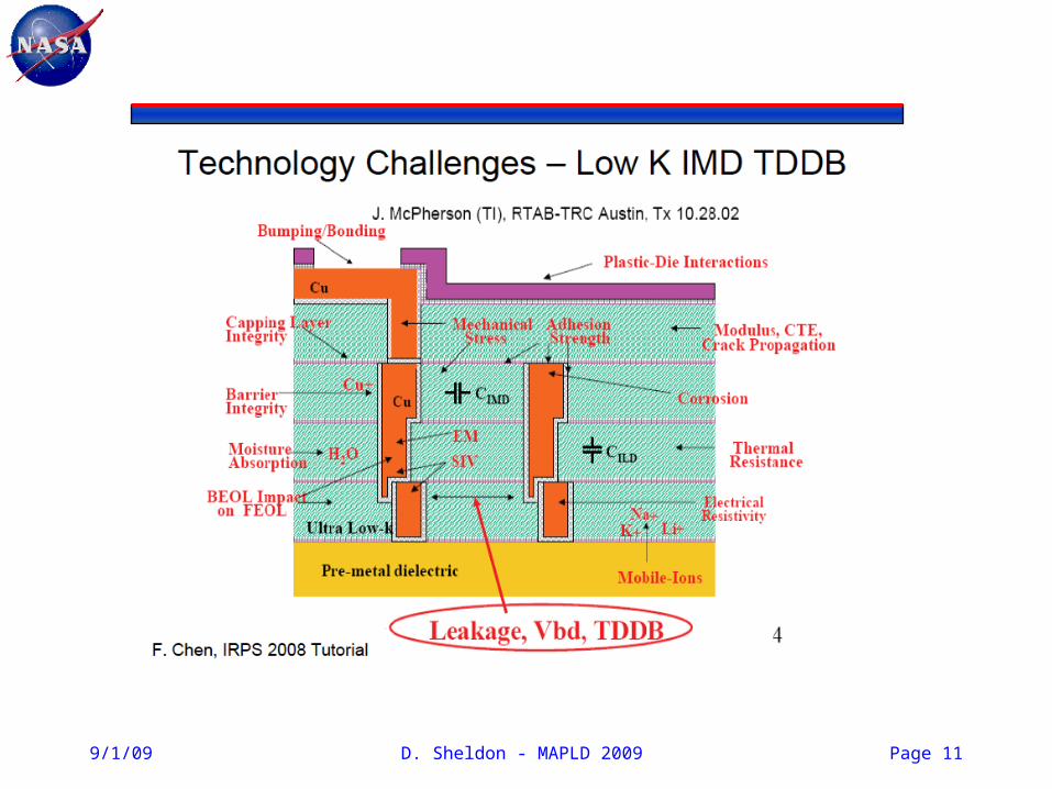
Scaling also means new materials => new reliability challenges
9/1/09 Page 12

D. Sheldon - MAPLD 2009
Modern approach to reliability in scaled devices like FPGAs
Page 139/1/09
V. Huard IRPS 2009 tutorial
Foundry & FPGA vendor
FPGA vendor &
User
D. Sheldon - MAPLD 2009
Scaling Examples
9/1/09 Page 14

D. Sheldon - MAPLD 2009
SiliconBlue FPGAs – NVM via Conductivity Modification – TSMC 65nm
9/1/09 Page 15
http://www.siliconbluetech.com/media/downloads/SBT_65LP_Process_Qual_v0.1.pdf
DC lifetime for Hot Carrier = 0.2yr

D. Sheldon - MAPLD 2009
Is it ok to run my FPGA at a higher than nominal Vdd?
• Example data and models from foundry:
• This example shows a clear reliability issue for that condition.• Manufacturer did additional functional and large sample size HTOL
at 1.2Vdd ± 10% and confirmed 5 year acceptance.• Not acceptable for long term, high reliability space mission.• Scaled technologies have reduced tolerance for “relatively” small
increases in voltage. Designs must have tighter control.
Page 169/1/09
IRPS Tutorial 2009 E. Hnatek and Y.W. Yau

D. Sheldon - MAPLD 2009
Negative Bias Temperature Instability - NBTI
• Complex electro-chemical degradation effect
• Interface trap generation and increased hole trapping mechanisms.
• Some of the degradation is recoverable after the stress is stopped.
• Magnitude of impact depends on circuit topology.
• Digital circuits most effected– Analog circuits will experience
some mismatch
• Both static and dynamic mitigation schemes to compensate for.
Page 179/1/09
A. Krishnan IRPS tutorial 2009

D. Sheldon - MAPLD 2009
NBTI with Xilinx Virtex 4
• DCM (digital clock management) circuits for managing clock skews and delays.– Designed to provide zero propagation delay and low clock skew.
• Accelerated life test show DCM maximum operating frequency will decline if DCM is held in a persistent (non) operating condition.– May not achieve lock at maximum frequency– Static stress creates small variations in duty cycle precision of multi
tap delay lines• Xilinx solutions involve:
– Null designs– Drop in macros for long duration operation– Automatic continuous configuration with updated ISE software
• Device level ageing effects can indeed impact system performance.
Page 189/1/09
http://www.xilinx.com/support/documentation/white_papers/wp224.pdf
http://www.xilinx.com/support/answers/21127.htm

D. Sheldon - MAPLD 2009
Scaling and Packages
• Scaling has significantly increased the the number of pins on modern IC packages.
• Wire bonding has given way to flip chip and wafer bump technologies for increased packing densities
Page 199/1/09

9/1/09 D. Sheldon - MAPLD 2009 20
Xilinx Virtex 2 Package Scaling Anomaly
• Anomaly occurred 28 times during launch level vibration on Y-axis only and did not at levels lower than launch levels
• After much detailed analysis fault identified as CS and RW shorting to together
Work done by JPL Tiger Team with Xilinx support
Scope Trace of Event Occurrences

D. Sheldon - MAPLD 2009
Sample Error Pattern for Anomalous Event
Expected Pattern
Anomalous Pattern
9/1/09 Page 21

Bond wire locations for shorting signals
D. Sheldon - MAPLD 2009 Page 22

9/1/09D. Sheldon - MAPLD 2009
Root Cause – Bond Wire Vibration
• Fundamental mode is a bending side-to-side of the loop
• Depends upon:– Bond wire diameter– Wire to wire spacing– Modulus of Elasticity and density of
material
• High Q~300 can lead to peak-to-peak displacements of a few wire diameters
• Original NASA related work: – M. Blakely, JPL & H. Leidecker, GSFC -
1998
0.151" pad-to-pad wire bond
0
500
1,000
1,500
2,000
2,500
3,000
0.000 0.020 0.040 0.060 0.080
Loop Height [inches]N
atu
ral F
req
ue
nc
y [
Hz]
Observed f
Page 23

D. Sheldon - MAPLD 2009
ESD and scaling
• ESD failures seem independent of HBM performance and device scaling (to first order).
• However scaling (higher speed, lower Vcc, lower breakdown V) makes same historical ESD requirements harder and harder to meet.
• Are historical standards still required?
• Industry council white paper recommends that reduced CDM goals must be adopted to adapt to scaling restrictions.
Page 24White paper 2: Industry Council on ESD Target Levels, 2009
R. Kwasnick, IRPS Tutorial , 2009
D. Sheldon - MAPLD 2009
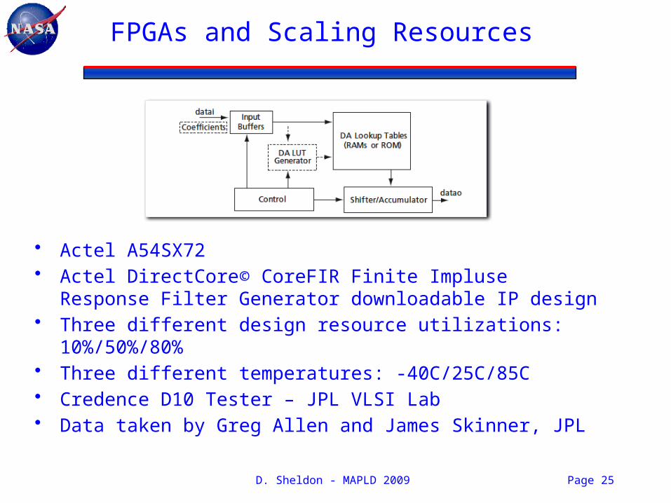
FPGAs and Scaling Resources
• Actel A54SX72• Actel DirectCore© CoreFIR Finite Impluse Response Filter
Generator downloadable IP design• Three different design resource utilizations: 10%/50%/80%• Three different temperatures: -40C/25C/85C• Credence D10 Tester – JPL VLSI Lab• Data taken by Greg Allen and James Skinner, JPL
Page 25

D. Sheldon - MAPLD 2009
Vcca Comparison Schmoos(same scale)
9/1/09 Page 26
50%/25C
80%/85C
D. Sheldon - MAPLD 2009
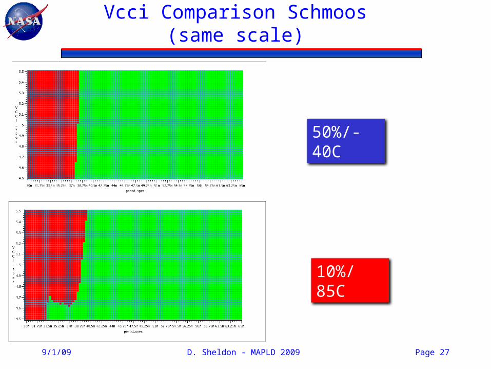
Vcci Comparison Schmoos(same scale)
9/1/09 Page 27
50%/-40C
10%/85C

D. Sheldon - MAPLD 2009
Timing vs. Temperature - Vcci
• Failing time increases linearly with temperature for designs ≥ 50%
• Increasing % resources used increases the slope of the temperature effect
Page 289/1/09
Nonlinear data

D. Sheldon - MAPLD 2009
Timing vs. Temperature - Vcca
• Increasing utilization increases sensitivity to temperature
• 10% design performance temperature independent
– More robust from reliability/mission assurance
– Small resource (array) contribution to total
• Need to trade mission requirements with reliability requirements
Page 29

D. Sheldon - MAPLD 2009
Scaling and JPL Mars FPGA Cost
Space FPGA cost increase 10X in 10 years
Page 309/1/09

D. Sheldon - MAPLD 2009
Thank you
Page 31
Recommended