1
Deposition and patterning
techniques for Organic
Semiconductors
Maddalena Binda
Organic Electronics: principles, devices and applications
Milano, November 15-18th, 2011
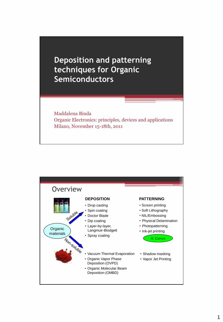
Overview
Organic
materials
DEPOSITION PATTERNING
• Drop casting
• Spin coating
• Doctor Blade
• Dip coating
• Layer-by-layer,
Langmuir-Blodgett
• Spray coating
• Screen printing
• Soft Lithography
• NIL/Embossing
• Physical Delamination
• Photopatterning
• Ink-jet printing
• Vacuum Thermal Evaporation
• Organic Vapor Phase
Deposition (OVPD)
• Organic Molecular Beam
Deposition (OMBD)
• Shadow masking
• Vapor Jet Printing
M. Caironi
2
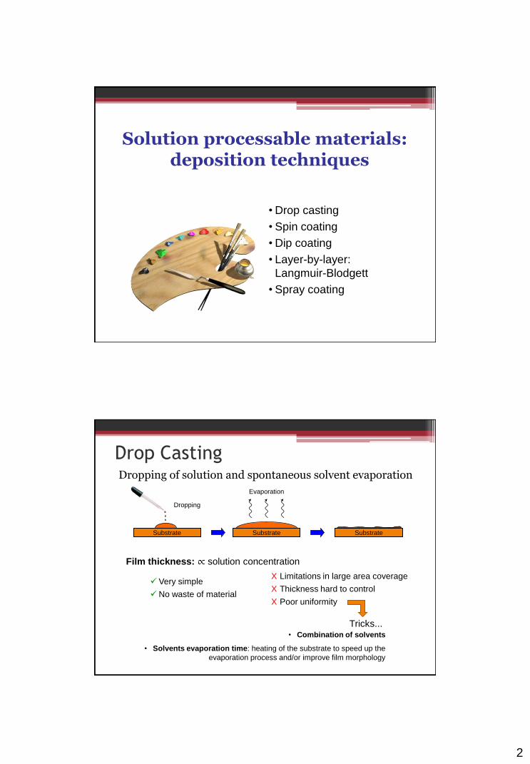
Solution processable materials: deposition techniques
• Drop casting
• Spin coating
• Dip coating
• Layer-by-layer:
Langmuir-Blodgett
• Spray coating
Drop Casting Dropping of solution and spontaneous solvent evaporation
Very simple
No waste of material
• Combination of solvents
• Solvents evaporation time: heating of the substrate to speed up the
evaporation process and/or improve film morphology
Dropping
Evaporation
Substrate Substrate Substrate
X Limitations in large area coverage
X Thickness hard to control
X Poor uniformity
Film thickness: solution concentration
Tricks...
3
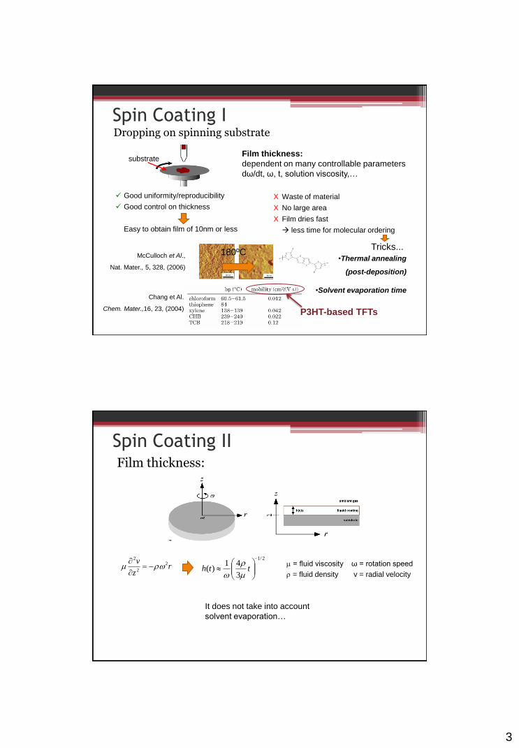
Spin Coating I Dropping on spinning substrate
Good uniformity/reproducibility
Good control on thickness
Easy to obtain film of 10nm or less
X Waste of material
X No large area
X Film dries fast
less time for molecular ordering
Film thickness:
dependent on many controllable parameters
dω/dt, ω, t, solution viscosity,…
•Thermal annealing
(post-deposition)
•Solvent evaporation time
McCulloch et Al.,
Nat. Mater., 5, 328, (2006)
substrate
Tricks... 180ºC
Chang et Al.
Chem. Mater.,16, 23, (2004) P3HT-based TFTs
Film thickness:
rz
v 2
2
2
2/1
3
41)(
tth
It does not take into account
solvent evaporation…
= fluid viscosity ω = rotation speed
= fluid density v = radial velocity
Spin Coating II
4
Film thickness:
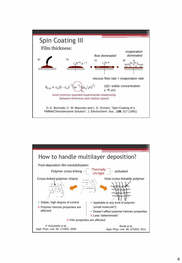
Spin Coating III
viscous flow rate = evaporation rate
c(t)= solids concentration
μ µ(t)
31
02
13
1
00 )()1(
cchFIN
D. E. Bornside, C. W. Macosko and L. E. Scriven, "Spin Coating of a
PMMA/Chlorobenzene Solution", J. Electrochem. Soc., 138, 317 (1991)
most common reported experimental relationship
between thickness and rotation speed
flow dominated
evaporation
dominated
How to handle multilayer deposition?
Post-deposition film insolubilization
Thermally
UV-light activated Polymer cross-linking
Host cross-linkable polymer Cross-linked polymer chains
Stable, high degree of control Appliable to any kind of polymer
(small molecule?)
Doesn’t affect polymer intrinsic properties
X Polymer intrinsic properties are
affected
X Less “deterministic”
X Film properties are affected
P. Keivanidis et al.,
Appl. Phys. Lett. 94, 173303, 2009. Binda et al.,
Appl. Phys. Lett. 98, 073303, 2011.
5
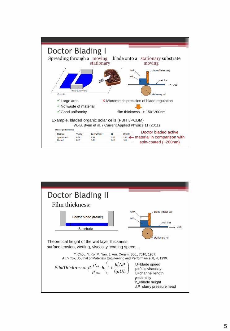
Doctor Blading I Spreading through a moving blade onto a stationary substrate
stationary moving
Large area
No waste of material
Good uniformity
X Micrometric precision of blade regulation
film thickness > 150÷200nm
Example. bladed organic solar cells (P3HT/PCBM)
W.-B. Byun et al. / Current Applied Physics 11 (2011)
Doctor bladed active
material in comparison with
spin-coated (~200nm)
Doctor Blading II
Theoretical height of the wet layer thickness:
surface tension, wetting, viscosity, coating speed,...
Film thickness:
Y. Chou, Y. Ko, M. Yan, J. Am. Ceram. Soc., 7010, 1987.
A.I.Y Tok, Journal of Materials Engineering and Performance, 8, 4, 1999.
UL
PhhessFilmThickn
film
sol
61
2
00
U=blade speed
µ=fluid viscosity
L=channel length
=density
ho=blade height
P=slurry pressure head
6
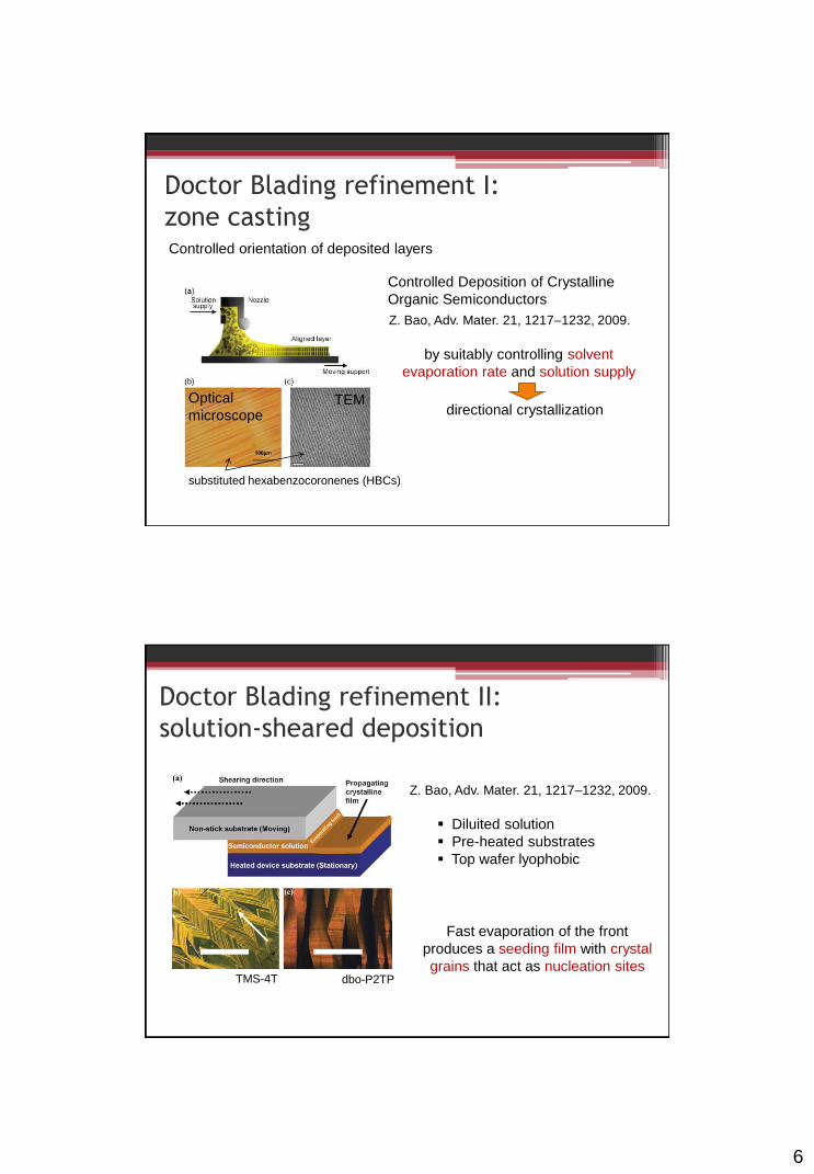
Doctor Blading refinement I:
zone casting Controlled orientation of deposited layers
Z. Bao, Adv. Mater. 21, 1217–1232, 2009.
Controlled Deposition of Crystalline
Organic Semiconductors
directional crystallization
by suitably controlling solvent
evaporation rate and solution supply
Optical
microscope TEM
substituted hexabenzocoronenes (HBCs)
Doctor Blading refinement II:
solution-sheared deposition
TMS-4T dbo-P2TP
Diluited solution
Pre-heated substrates
Top wafer lyophobic
Fast evaporation of the front
produces a seeding film with crystal
grains that act as nucleation sites
Z. Bao, Adv. Mater. 21, 1217–1232, 2009.
7
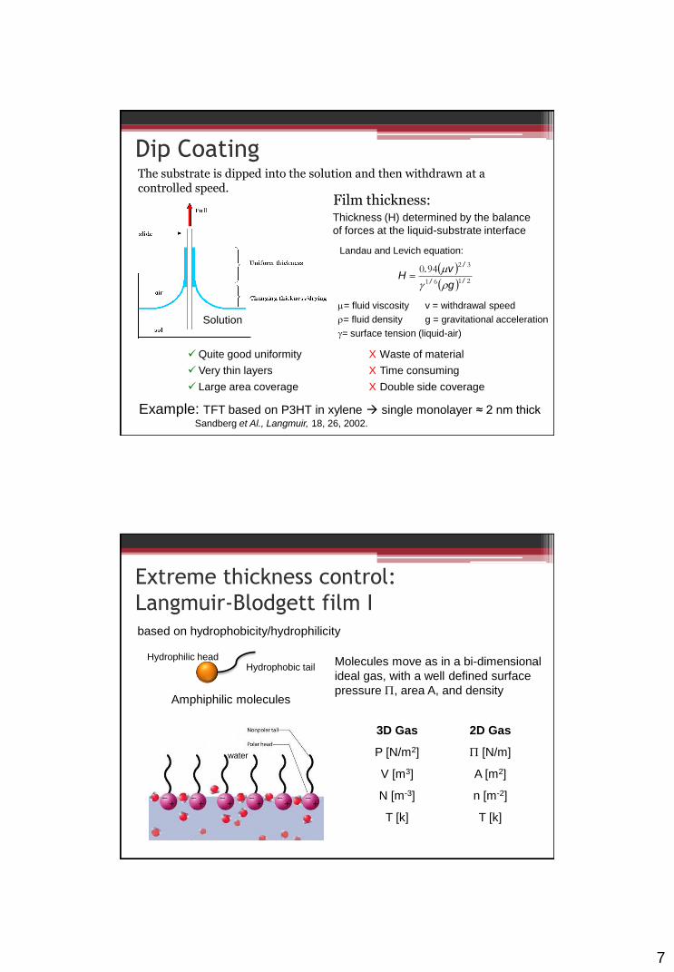
Dip Coating The substrate is dipped into the solution and then withdrawn at a controlled speed.
Thickness (H) determined by the balance
of forces at the liquid-substrate interface
Solution
Film thickness:
Landau and Levich equation:
2161
32940
//
/
g
v.H
= fluid viscosity v = withdrawal speed
= fluid density g = gravitational acceleration
= surface tension (liquid-air)
Quite good uniformity
Very thin layers
Large area coverage
X Waste of material
X Time consuming
X Double side coverage
Sandberg et Al., Langmuir, 18, 26, 2002.
Example: TFT based on P3HT in xylene single monolayer ≈ 2 nm thick
water
Molecules move as in a bi-dimensional
ideal gas, with a well defined surface
pressure P, area A, and density
3D Gas
P [N/m2]
V [m3]
N [m-3]
T [k]
2D Gas
P [N/m]
A [m2]
n [m-2]
T [k]
based on hydrophobicity/hydrophilicity
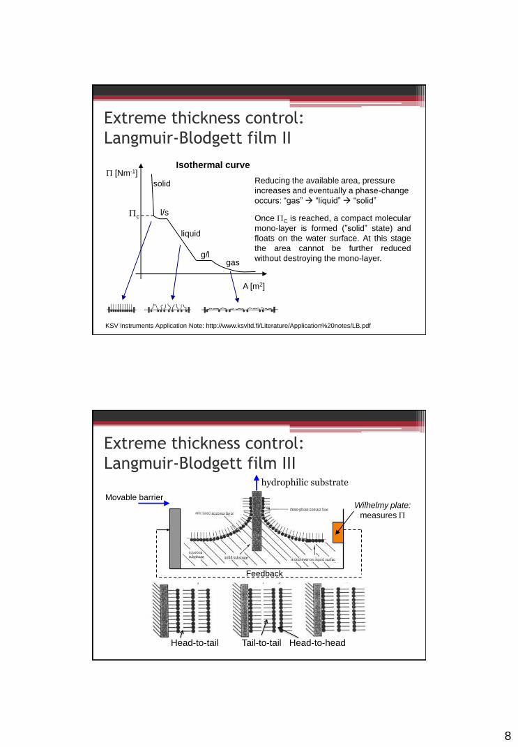
Extreme thickness control:
Langmuir-Blodgett film I
Amphiphilic molecules
Hydrophilic head Hydrophobic tail
8
Extreme thickness control:
Langmuir-Blodgett film II
Reducing the available area, pressure
increases and eventually a phase-change
occurs: “gas” “liquid” “solid”
A [m2]
P [Nm-1]
gas
liquid
solid
g/l
l/s Pc Once PC is reached, a compact molecular
mono-layer is formed (”solid” state) and
floats on the water surface. At this stage
the area cannot be further reduced
without destroying the mono-layer.
KSV Instruments Application Note: http://www.ksvltd.fi/Literature/Application%20notes/LB.pdf
Isothermal curve
hydrophilic substrate
Movable barrier Wilhelmy plate:
measures P
Feedback
Extreme thickness control:
Langmuir-Blodgett film III
Head-to-tail Head-to-head Tail-to-tail
9
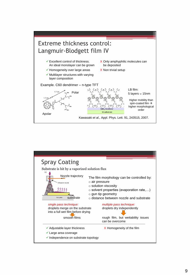
Example. C60 dendrimer – n-type TFT
LB film:
5 layers 15nm
Apolar
Polar
Kawasaki et al., Appl. Phys. Lett. 91, 243515, 2007.
Higher mobility than
spin-coated film
higher morphological
order
Extreme thickness control:
Langmuir-Blodgett film IV
Excellent control of thickness.
An ideal monolayer can be grown
Homogeneity over large areas
Multilayer structures with varying
layer composition
X Only amphyphilic molecules can
be deposited
X Non trivial setup
Spray Coating
single pass technique:
droplets merge on the substrate
into a full wet film before drying
smooth films
The film morphology can be controlled by:
o air pressure
o solution viscosity
o solvent properties (evaporation rate,…)
o gun tip geometry
o distance between nozzle and substrate
Substrate is hit by a vaporized solution flux
multiple pass technique:
droplets dry independently
rough film, but wettability issues
can be overcome
substrate
Nozzle trajectory
Adjustable layer thickness
Large area coverage
Independence on substrate topology
X Homogeneity of the film
10
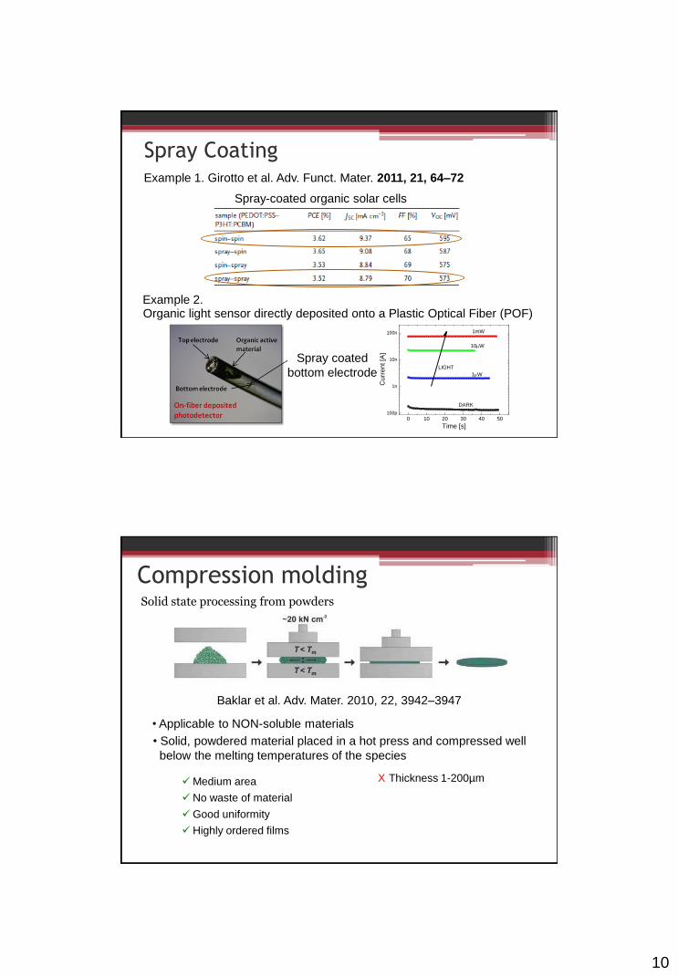
Spray Coating Example 1. Girotto et al. Adv. Funct. Mater. 2011, 21, 64–72
Spray-coated organic solar cells
Example 2. Organic light sensor directly deposited onto a Plastic Optical Fiber (POF)
Spray coated
bottom electrode
0 10 20 30 40 50100p
1n
10n
100n
Cu
rre
nt [A
]
Time [s]
DARK
LIGHT
1mW
10W
1W
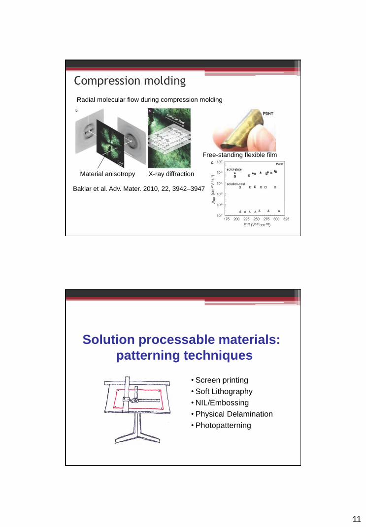
Baklar et al. Adv. Mater. 2010, 22, 3942–3947
Compression molding Solid state processing from powders
• Applicable to NON-soluble materials
• Solid, powdered material placed in a hot press and compressed well
below the melting temperatures of the species
Medium area
No waste of material
Good uniformity
Highly ordered films
X Thickness 1-200µm
11
Compression molding
Free-standing flexible film
Radial molecular flow during compression molding
Baklar et al. Adv. Mater. 2010, 22, 3942–3947
Material anisotropy X-ray diffraction
Solution processable materials:
patterning techniques
• Screen printing
• Soft Lithography
• NIL/Embossing
• Physical Delamination
• Photopatterning
12
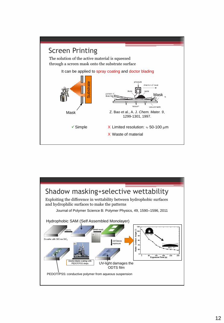
Screen Printing The solution of the active material is squeezed
through a screen mask onto the substrate surface
Mask
Substr
ate
X Limited resolution: 50-100 m
X Waste of material
It can be applied to spray coating and doctor blading
Simple
Mask
Z. Bao et al., A. J. Chem. Mater. 9,
1299-1301, 1997.
Shadow masking+selective wettability Exploiting the difference in wettability between hydrophobic surfaces and hydrophilic surfaces to make the patterns
UV-light damages the
ODTS film
Journal of Polymer Science B: Polymer Physics, 49, 1590–1596, 2011
PEDOT/PSS: conductive polymer from aqueous suspension
Hydrophobic SAM (Self Assembled Monolayer)
13
Journal of Polymer Science B: Polymer Physics, 49, 1590–1596, 2011
Shadow masking+selective wettability
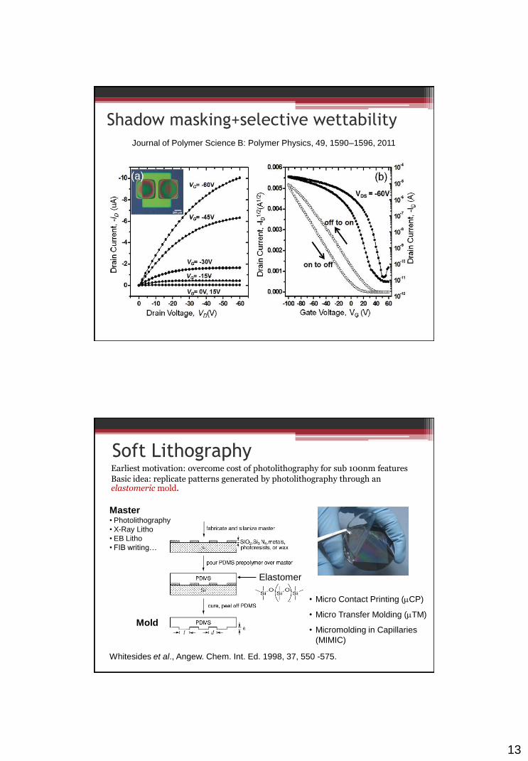
Soft Lithography Earliest motivation: overcome cost of photolithography for sub 100nm features
Basic idea: replicate patterns generated by photolithography through an elastomeric mold.
Master • Photolithography
• X-Ray Litho
• EB Litho
• FIB writing…
Mold
Elastomer
• Micro Contact Printing (CP)
• Micro Transfer Molding (TM)
• Micromolding in Capillaries
(MIMIC)
Whitesides et al., Angew. Chem. Int. Ed. 1998, 37, 550 -575.
14
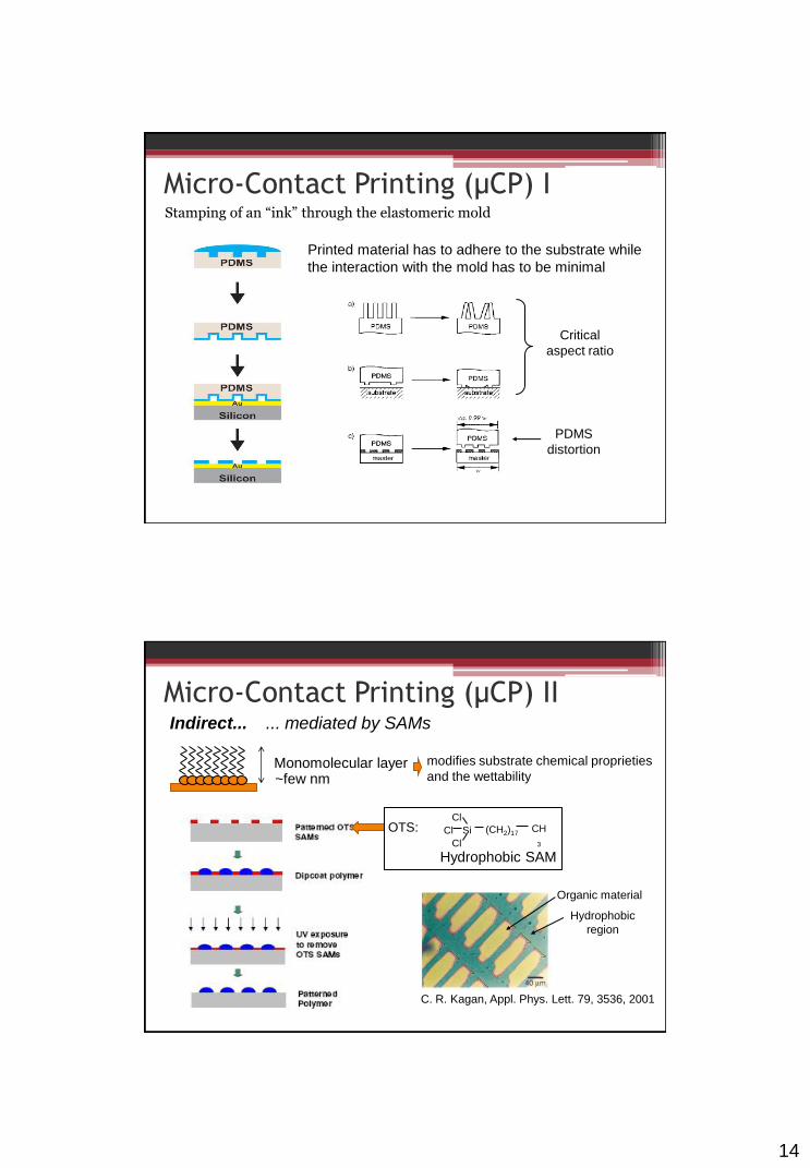
Micro-Contact Printing (µCP) I Stamping of an “ink” through the elastomeric mold
Critical
aspect ratio
PDMS
distortion
Printed material has to adhere to the substrate while
the interaction with the mold has to be minimal
modifies substrate chemical proprieties
and the wettability
Micro-Contact Printing (µCP) II Indirect... ... mediated by SAMs
~few nm Monomolecular layer
OTS: Cl
Si
Cl
Cl (CH2)17 CH
3
Hydrophobic SAM
Organic material
Hydrophobic
region
C. R. Kagan, Appl. Phys. Lett. 79, 3536, 2001
15
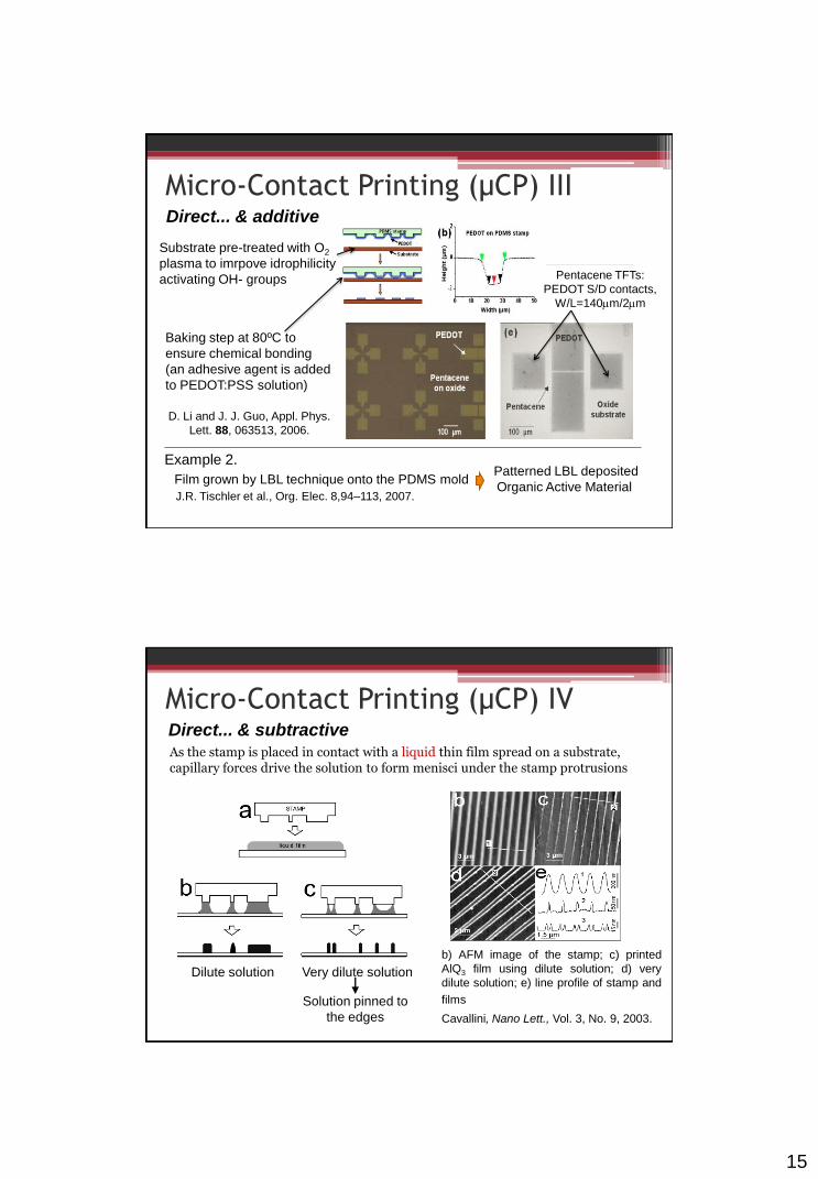
Micro-Contact Printing (µCP) III Direct... & additive
Pentacene TFTs:
PEDOT S/D contacts,
W/L=140m/2m
D. Li and J. J. Guo, Appl. Phys.
Lett. 88, 063513, 2006.
Substrate pre-treated with O2
plasma to imrpove idrophilicity
activating OH- groups
Baking step at 80ºC to
ensure chemical bonding
(an adhesive agent is added
to PEDOT:PSS solution)
J.R. Tischler et al., Org. Elec. 8,94–113, 2007.
Film grown by LBL technique onto the PDMS mold Patterned LBL deposited
Organic Active Material
Example 2.
Micro-Contact Printing (µCP) IV Direct... & subtractive
As the stamp is placed in contact with a liquid thin film spread on a substrate, capillary forces drive the solution to form menisci under the stamp protrusions
Dilute solution Very dilute solution
Solution pinned to
the edges
b) AFM image of the stamp; c) printed
AlQ3 film using dilute solution; d) very
dilute solution; e) line profile of stamp and
films
Cavallini, Nano Lett., Vol. 3, No. 9, 2003.
16
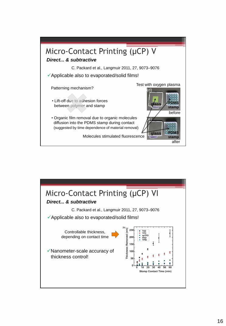
Micro-Contact Printing (µCP) V Direct... & subtractive
C. Packard et al., Langmuir 2011, 27, 9073–9076
Applicable also to evaporated/solid films!
Patterning mechanism?
• Lift-off due to adhesion forces
between polymer and stamp
• Organic film removal due to organic molecules
diffusion into the PDMS stamp during contact
(suggested by time dependence of material removal)
Test with oxygen plasma
before
after
glass
glass
PDMS
stamp
PDMS
stamp Molecules stimulated fluorescence
Micro-Contact Printing (µCP) VI Direct... & subtractive
C. Packard et al., Langmuir 2011, 27, 9073–9076
Applicable also to evaporated/solid films!
Controllable thickness,
depending on contact time
Nanometer-scale accuracy of
thickness control!
17
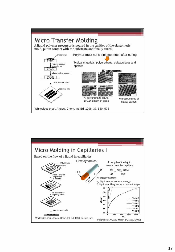
Micro Transfer Molding A liquid polymer precursor is poured in the cavities of the elastomeric mold, put in contact with the substrate and finally cured.
Typical materials: polyurethane, polyacrylates and
epoxies
A: polyurethane on Ag,
B,C,D: epoxy on glass Microstructures of
glassy carbon
3D structures
Whitesides et al., Angew. Chem. Int. Ed. 1998, 37, 550 -575
Polymer must not shrink too much after curing
Micro Molding in Capillaries I Based on the flow of a liquid in capillaries
Flow dynamics:
Z
2R
Z: length of the liquid
column into the capillary
Z
cosR
dt
dZ lv
4
: liquid viscosity
lv: liquid-vapor surface energy
θ: liquid-capillary surface contact angle
L
Whitesides et al., Angew. Chem. Int. Ed. 1998, 37, 550 -575 Pisignano et Al., Adv. Mater. 14, 1565, (2002)
18
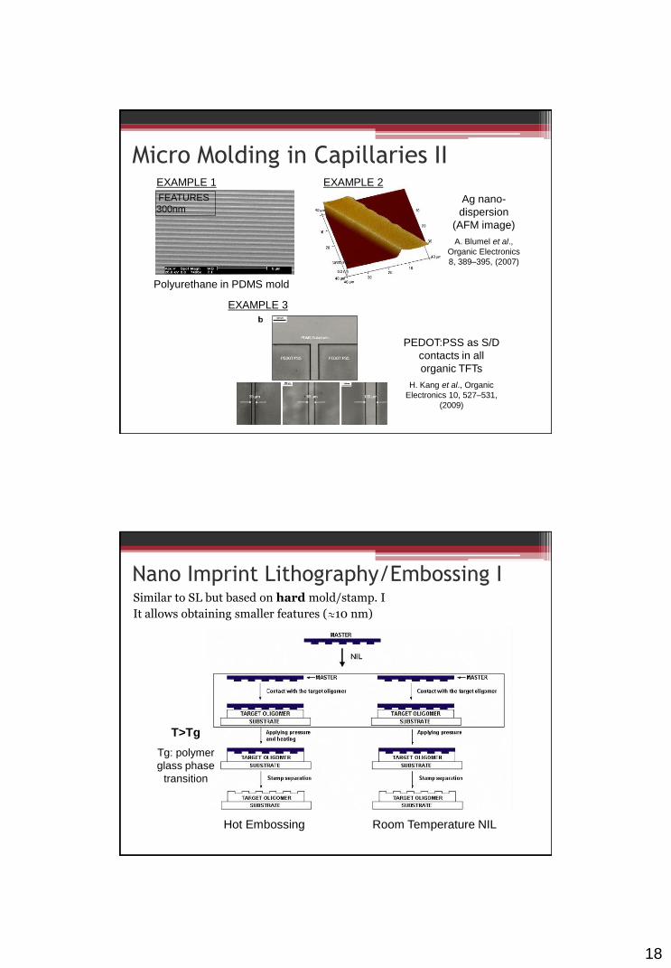
Micro Molding in Capillaries II
• Examples:
FEATURES
300nm
Polyurethane in PDMS mold
PEDOT:PSS as S/D
contacts in all
organic TFTs
H. Kang et al., Organic
Electronics 10, 527–531,
(2009)
Ag nano-
dispersion
(AFM image)
A. Blumel et al.,
Organic Electronics
8, 389–395, (2007)
EXAMPLE 1 EXAMPLE 2
EXAMPLE 3
Nano Imprint Lithography/Embossing I Similar to SL but based on hard mold/stamp. I
It allows obtaining smaller features ( 10 nm)
Hot Embossing Room Temperature NIL
T>Tg
Tg: polymer
glass phase
transition
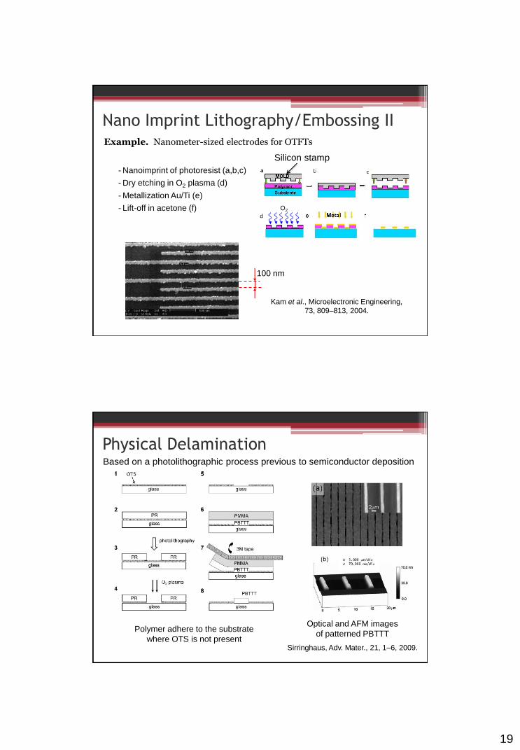
19
Example. Nanometer-sized electrodes for OTFTs
- Nanoimprint of photoresist (a,b,c)
- Dry etching in O2 plasma (d)
- Metallization Au/Ti (e)
- Lift-off in acetone (f) d
O2
100 nm
Kam et al., Microelectronic Engineering,
73, 809–813, 2004.
Nano Imprint Lithography/Embossing II
Silicon stamp
Physical Delamination Based on a photolithographic process previous to semiconductor deposition
Polymer adhere to the substrate
where OTS is not present
Optical and AFM images
of patterned PBTTT
Sirringhaus, Adv. Mater., 21, 1–6, 2009.
20
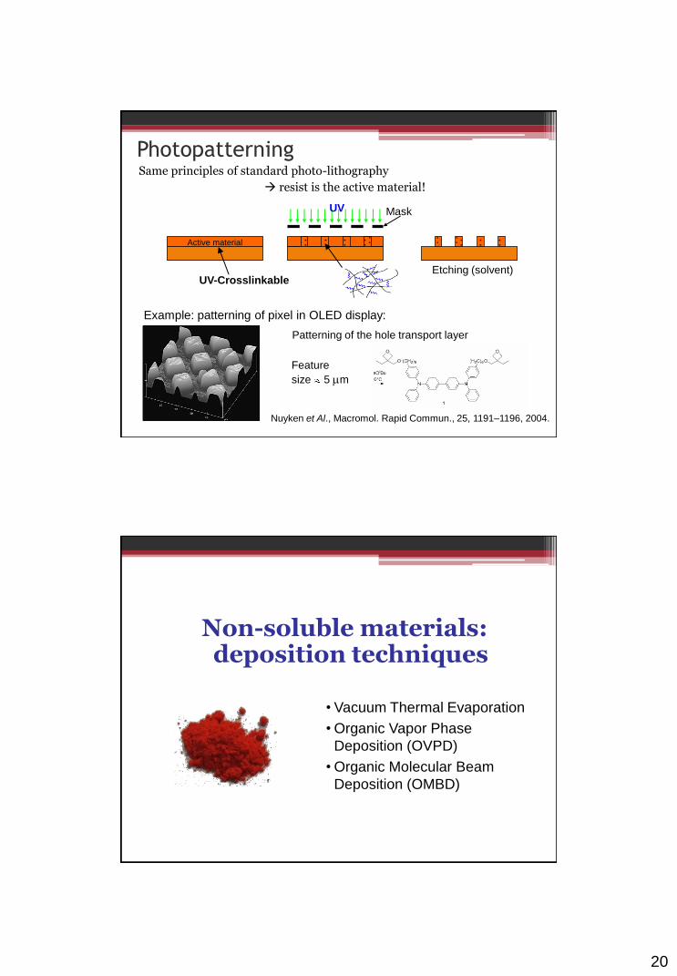
Photopatterning Same principles of standard photo-lithography
resist is the active material!
Example: patterning of pixel in OLED display:
Nuyken et Al., Macromol. Rapid Commun., 25, 1191–1196, 2004.
Patterning of the hole transport layer
Feature
size 5 m
Active material
UV-Crosslinkable
UV Mask
Etching (solvent)
Non-soluble materials: deposition techniques
• Vacuum Thermal Evaporation
• Organic Vapor Phase
Deposition (OVPD)
• Organic Molecular Beam
Deposition (OMBD)
21
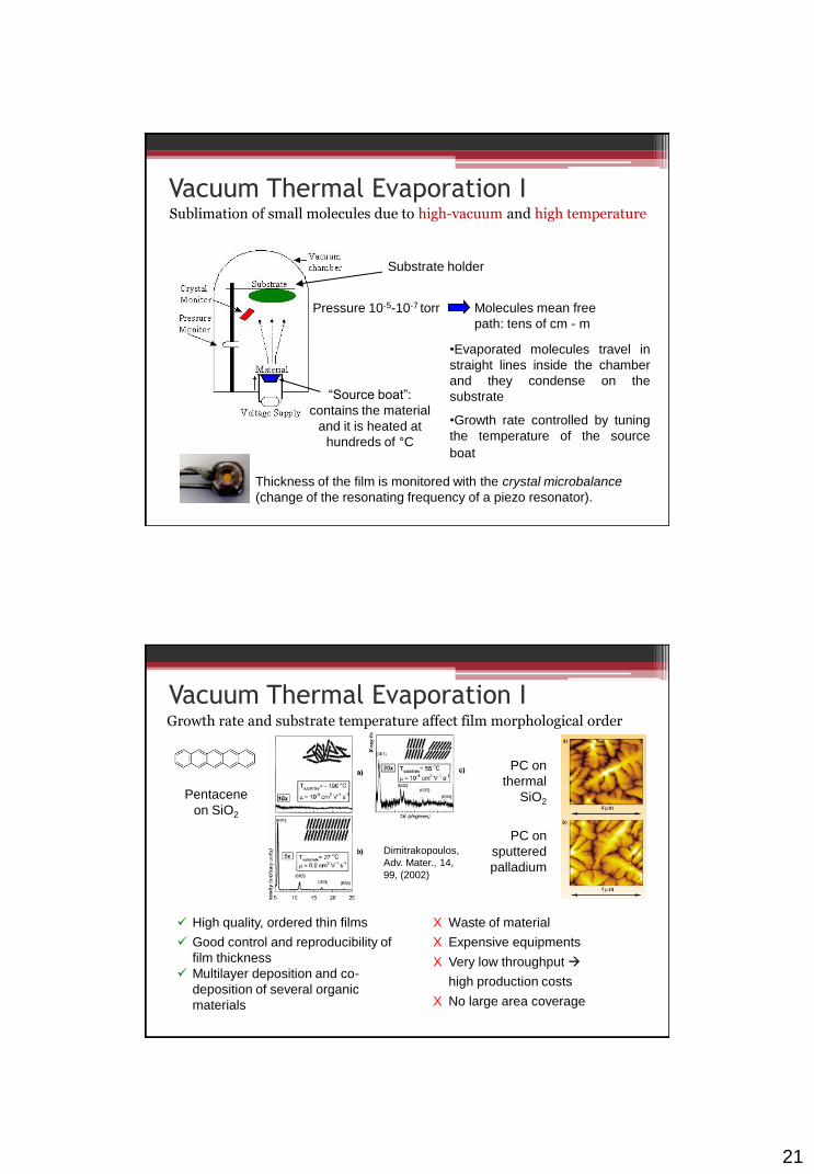
Vacuum Thermal Evaporation I Sublimation of small molecules due to high-vacuum and high temperature
Pressure 10-5-10-7 torr Molecules mean free
path: tens of cm - m
“Source boat”:
contains the material
and it is heated at
hundreds of °C
Thickness of the film is monitored with the crystal microbalance
(change of the resonating frequency of a piezo resonator).
Substrate holder
•Evaporated molecules travel in
straight lines inside the chamber
and they condense on the
substrate
•Growth rate controlled by tuning
the temperature of the source
boat
Growth rate and substrate temperature affect film morphological order
High quality, ordered thin films
Good control and reproducibility of
film thickness
Multilayer deposition and co-
deposition of several organic
materials
X Waste of material
X Expensive equipments
X Very low throughput
high production costs
X No large area coverage
Pentacene
on SiO2
PC on
thermal
SiO2
PC on
sputtered
palladium
Dimitrakopoulos,
Adv. Mater., 14,
99, (2002)
Vacuum Thermal Evaporation I
22
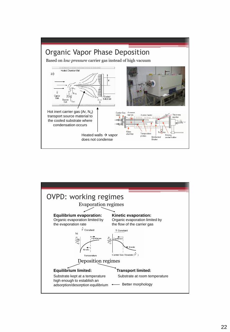
Organic Vapor Phase Deposition Based on low pressure carrier gas instead of high vacuum
Hot inert carrier gas (Ar, N2)
transport source material to
the cooled substrate where
condensation occurs
Heated walls vapor
does not condense
OVPD: working regimes Evaporation regimes
Equilibrium evaporation: Kinetic evaporation:
Deposition regimes
Equilibrium limited: Transport limited:
Organic evaporation limited by
the evaporation rate
Organic evaporation limited by
the flow of the carrier gas
Substrate kept at a temperature
high enough to establish an
adsorption/desorption equilibrium
Substrate at room temperature
Better morphology
23
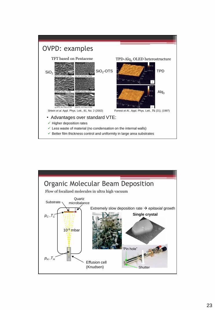
OVPD: examples
TFT based on Pentacene
Higher deposition rates
Less waste of material (no condensation on the internal walls)
Better film thickness control and uniformity in large area substrates
• Advantages over standard VTE:
SiO2 SiO2-OTS
TPD-Alq3 OLED heterostructure
Forrest et Al., Appl. Phys. Lett., 71 (21), (1997)
TPD
Alq3
Shtein et al. Appl. Phys. Lett., 81, No. 2 (2002)
Organic Molecular Beam Deposition Flow of focalized molecules in ultra high vacuum
pC ,TC
Quartz
microbalance
pH ,TH
Substrate
Effusion cell
(Knudsen)
“Pin hole”
Shutter
10-9 mbar
Single crystal
Extremely slow deposition rate epitaxial growth
24
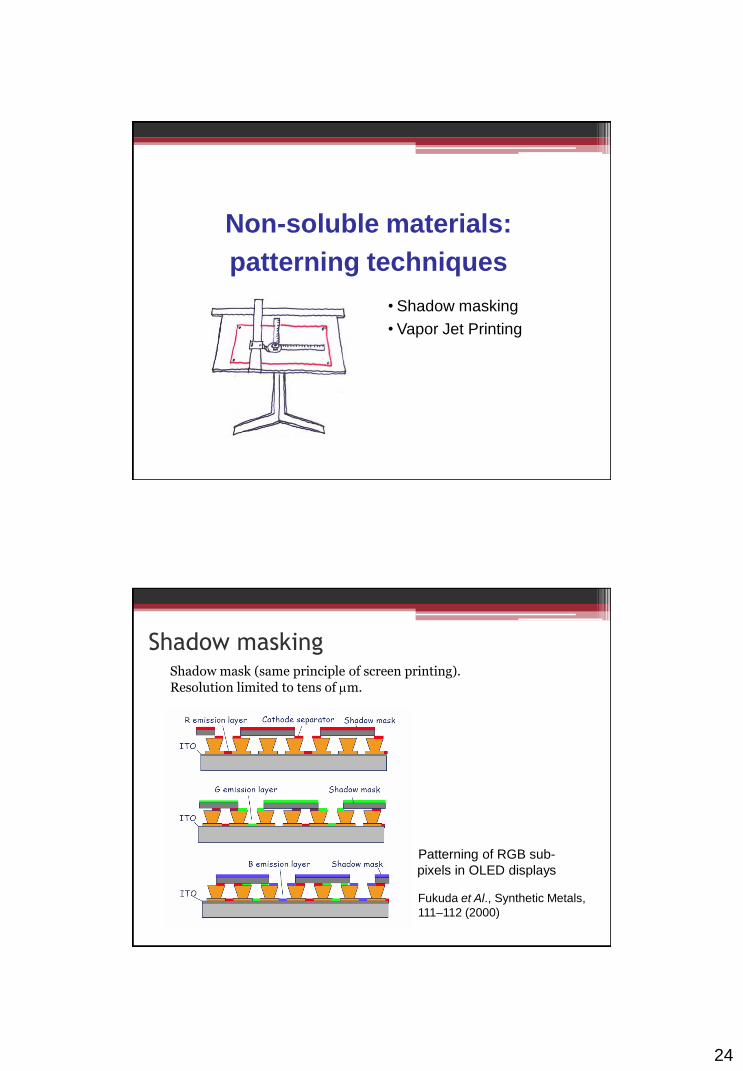
Non-soluble materials:
patterning techniques
• Shadow masking
• Vapor Jet Printing
Shadow masking Shadow mask (same principle of screen printing).
Resolution limited to tens of m.
Patterning of RGB sub-
pixels in OLED displays
Fukuda et Al., Synthetic Metals,
111–112 (2000)
25
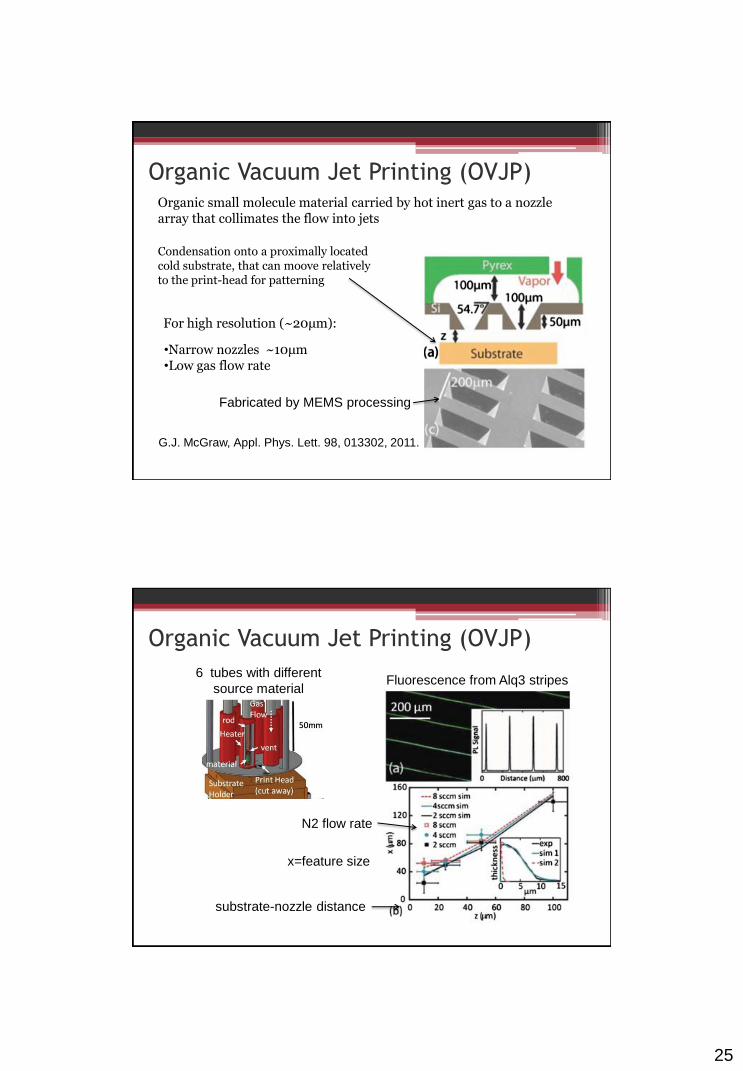
Organic Vacuum Jet Printing (OVJP)
G.J. McGraw, Appl. Phys. Lett. 98, 013302, 2011.
Organic small molecule material carried by hot inert gas to a nozzle array that collimates the flow into jets
Condensation onto a proximally located cold substrate, that can moove relatively to the print-head for patterning
•Narrow nozzles ~10μm •Low gas flow rate
Fabricated by MEMS processing
For high resolution (~20μm):
Organic Vacuum Jet Printing (OVJP)
Fluorescence from Alq3 stripes
substrate-nozzle distance
x=feature size
N2 flow rate
6 tubes with different
source material
Recommended