06/2009 | Fundamentals of DSOs | 1 Nov 2010 | Scope Seminar – Signal Fidelity | 1
1
Debugging EMI Using a Digital Oscilloscope
06/2009 | Fundamentals of DSOs | 2 Nov 2010 | Scope Seminar – Signal Fidelity | 2
2
Debugging EMI Using a Digital Oscilloscope
l Background – radiated emissions l Basics of near field probing l EMI debugging process l Frequency domain analysis using an oscilloscope
l FFT computation l Dynamic range and sensitivity l Time gating l Frequency domain triggering
l Measurement example
06/2009 | Fundamentals of DSOs | 3 Nov 2010 | Scope Seminar – Signal Fidelity | 3
3
The Problem: isolating sources of EMI
l EMI compliance is tested in the RF far field l Compliance is based on specific allowable power levels as a
function of frequency using a specific antenna, resolution bandwidth and distance from the DUT
l No localization of specific emitters within the DUT l What happens when compliance fails?
l Need to locate where the offending emitter is within the DUT l Local probing in the near field (close to the DUT) can help physically
locate the problem l Remediate using shielding or by reducing the EM radiation
l How do we find the source? l Frequency domain measurement l Time/frequency domain measurement l Localizing in space
Basic Principles: Radiated Emissions The following conditions must exist ı An interference source exists that generates a sufficiently high
disturbance level in a frequency range that is relevant for RF emissions (e.g. fast switching edges) ı There is a coupling mechanism that transmits the generated
disturbance signals from the interference source to the emitting element ı There is some emitting element that is capable of radiating the
energy produced by the source into the far field (e.g. a connected cable, slots in the enclosure or a printed circuit board that acts as an antenna)
March 2013 EMI Debugging with the RTO 4
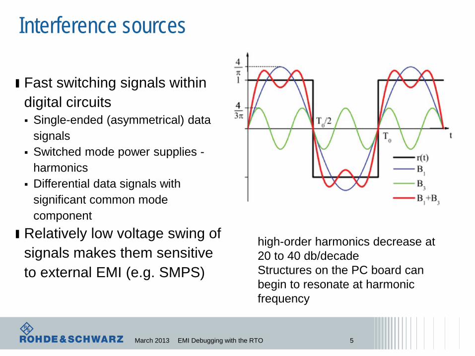
Interference sources
ı Fast switching signals within digital circuits Single-ended (asymmetrical) data
signals Switched mode power supplies -
harmonics Differential data signals with
significant common mode component
ı Relatively low voltage swing of signals makes them sensitive to external EMI (e.g. SMPS)
March 2013 EMI Debugging with the RTO 5
high-order harmonics decrease at 20 to 40 db/decade Structures on the PC board can begin to resonate at harmonic frequency

Differential Mode RF Emissions
ı Emission results when signal and return are not routed together ı Near field probe can detect
this by positioning within the loop – position of probe is critical ı Mitigate by routing signal
and ground closer, reducing signal current or decreasing slew rate
March 2013 EMI Debugging with the RTO 6
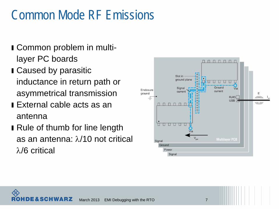
Common Mode RF Emissions
ı Common problem in multi-layer PC boards ı Caused by parasitic
inductance in return path or asymmetrical transmission ı External cable acts as an
antenna ı Rule of thumb for line length
as an antenna: λ/10 not critical λ/6 critical
March 2013 EMI Debugging with the RTO 7
General steps to help reduce common-mode RF emissions
ı Reduce the RFI current ICM by optimizing the layout, reducing
the ground plane impedances or rearranging components ı Reduce higher-frequency signal components through filtering or
by reducing the rise and fall times of digital signals ı Use shielding (lines, enclosures, etc.) ı Optimize the signal integrity to reduce unwanted overshoots
(ringing)
March 2013 EMI Debugging with the RTO 8
Coupling Mechanisms
ı Three coupling paths: Direct RF emissions from the source, e.g. from a trace or an individual
component RF emissions via connected power supply, data or signal lines Conducted emission via connected power supply, data or signal lines ı Coupling Mechanisms Coupling via a common impedance Electric field coupling – parasitic capacitance between source and antenna Magnetic field coupling – parasitic inductance between source and antenna Electromagnetic coupling – far field coupling (greater than 1 wavelength)
March 2013 EMI Debugging with the RTO 9
Emitting Elements (Antennas)
ıMain types of unintentional antennas in electronic equipment ı Connected lines (power supply, data/signal/control lines) ı Printed circuit board tracks and planes ı Internal cables between system components ı Components and heat sinks ı Slots and openings in enclosures
March 2013 EMI Debugging with the RTO 10
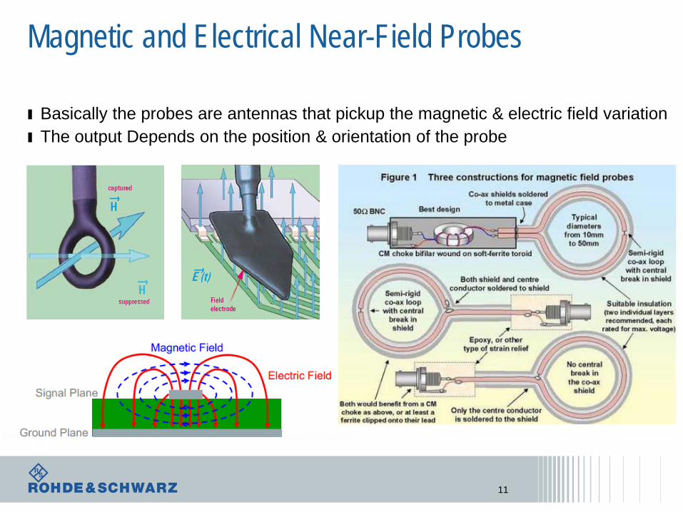
Magnetic and Electrical Near-Field Probes
11
ı Basically the probes are antennas that pickup the magnetic & electric field variation ı The output Depends on the position & orientation of the probe
06/2009 | Fundamentals of DSOs | 12 Nov 2010 | Scope Seminar – Signal Fidelity | 12
12
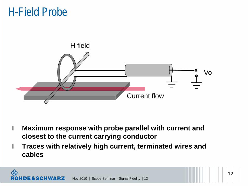
H-Field Probe
l Maximum response with probe parallel with current and closest to the current carrying conductor
l Traces with relatively high current, terminated wires and cables
Current flow
H field
Vo
06/2009 | Fundamentals of DSOs | 13 Nov 2010 | Scope Seminar – Signal Fidelity | 13
13
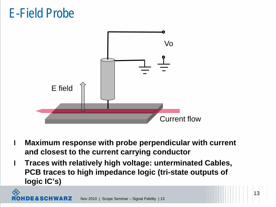
E-Field Probe
l Maximum response with probe perpendicular with current and closest to the current carrying conductor
l Traces with relatively high voltage: unterminated Cables, PCB traces to high impedance logic (tri-state outputs of logic IC’s)
Current flow
E field
Vo
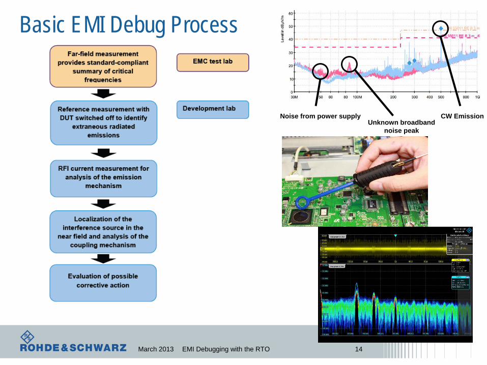
Basic EMI Debug Process
March 2013 EMI Debugging with the RTO 14
CW Emission Unknown broadband
noise peak
Noise from power supply
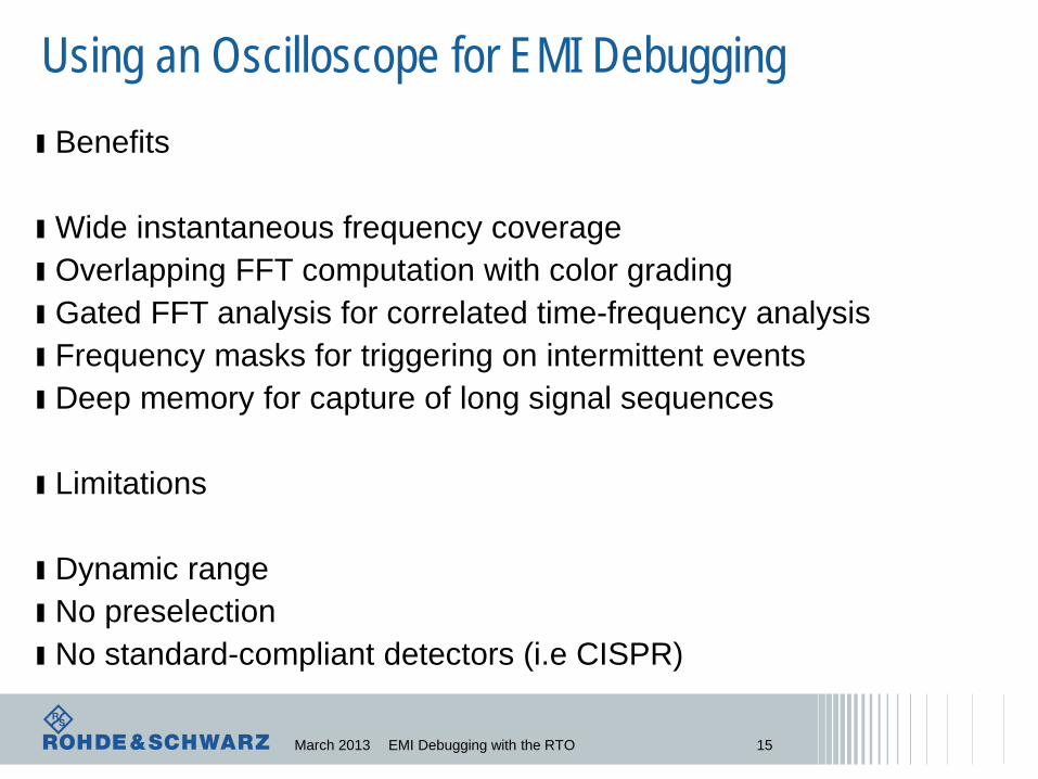
Using an Oscilloscope for EMI Debugging ı Benefits
ı Wide instantaneous frequency coverage ı Overlapping FFT computation with color grading ı Gated FFT analysis for correlated time-frequency analysis ı Frequency masks for triggering on intermittent events ı Deep memory for capture of long signal sequences
ı Limitations
ı Dynamic range ı No preselection ı No standard-compliant detectors (i.e CISPR)
March 2013 EMI Debugging with the RTO 15
06/2009 | Fundamentals of DSOs | 16 Nov 2010 | Scope Seminar – Signal Fidelity | 16
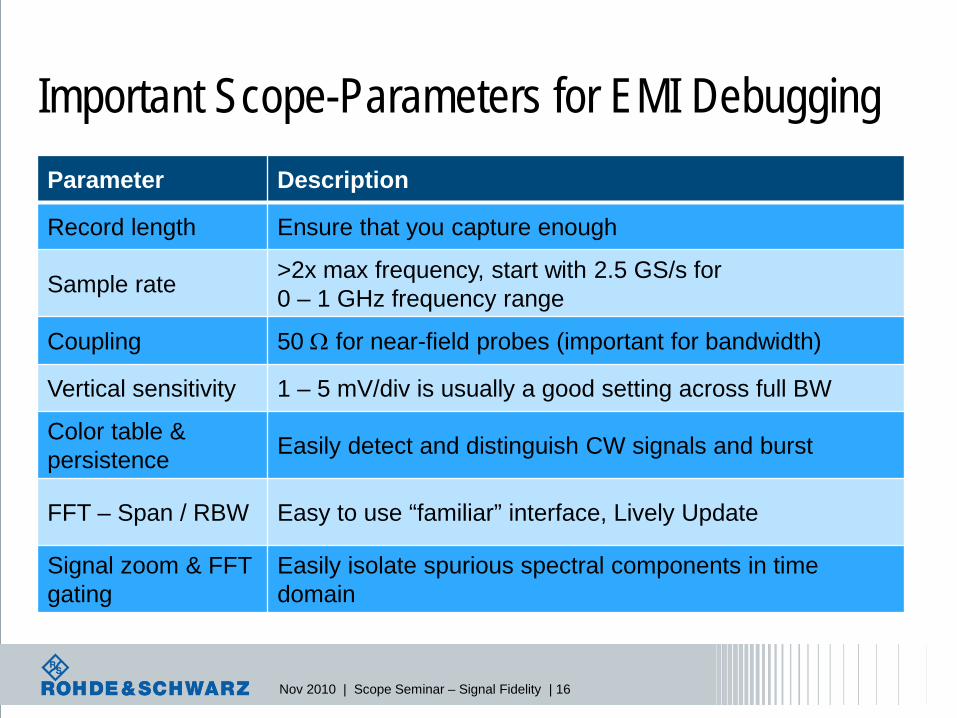
Important Scope-Parameters for EMI Debugging Parameter Description
Record length Ensure that you capture enough
Sample rate >2x max frequency, start with 2.5 GS/s for 0 – 1 GHz frequency range
Coupling 50 Ω for near-field probes (important for bandwidth)
Vertical sensitivity 1 – 5 mV/div is usually a good setting across full BW
Color table & persistence Easily detect and distinguish CW signals and burst
FFT – Span / RBW Easy to use “familiar” interface, Lively Update
Signal zoom & FFT gating
Easily isolate spurious spectral components in time domain
17
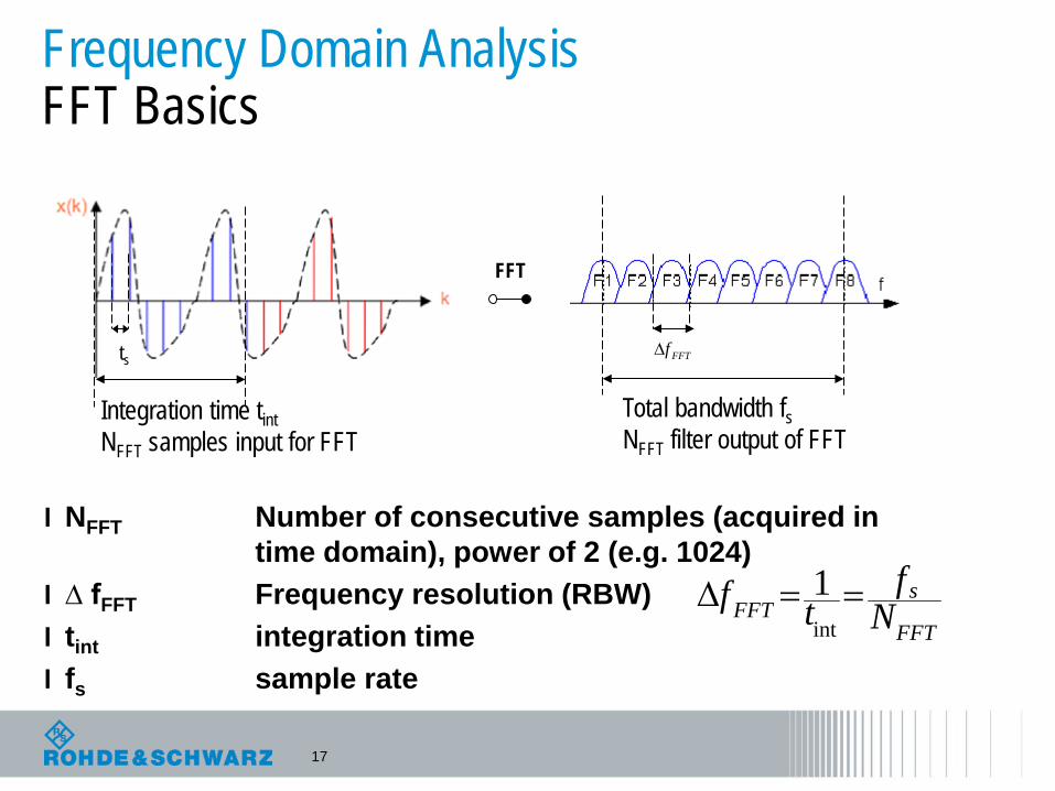
Frequency Domain Analysis FFT Basics
l NFFT Number of consecutive samples (acquired in time domain), power of 2 (e.g. 1024)
l ∆ fFFT Frequency resolution (RBW) l tint integration time l fs sample rate
FFT
sFFT N
ftf ==∆int
1
Integration time tint NFFT samples input for FFT
FFT
Total bandwidth fs NFFT filter output of FFT
FFTf∆ts
FFT as Basis for EMI Debugging with Oscilloscopes Conventional FFT Implementation on a Scope
21.03.2013 18
t
Time Domain
Record length T
Windowing FFT
Data acquisition
Zoom (f1…f2) f
Frequency Domain
∆t = 1/Fs
f
Display f2 f1
Fmax = Fs/2
S(f) S(f) x(t)
∆f = 1/T
Disadvantages: Time domain settings define frequency domain Zoom in frequency domain does not give more details Correlated Time-Frequency Analysis not possible
f1 f2
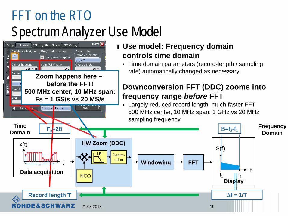
FFT on the RTO Spectrum Analyzer Use Model
ı Use model: Frequency domain controls time domain Time domain parameters (record-length / sampling
rate) automatically changed as necessary
ı Downconversion FFT (DDC) zooms into frequency range before FFT Largely reduced record length, much faster FFT
500 MHz center, 10 MHz span: 1 GHz vs 20 MHz sampling frequency
Time Domain
t
Record length T
Data acquisition
Fs=2Β
x(t)
Frequency Domain
f
Display f2 f1
Β=f2-f1
S(f)
∆f = 1/T
Windowing FFT
21.03.2013 19
HW Zoom (DDC)
NCO
Decim- ation
LP
Zoom happens here – before the FFT!
500 MHz center, 10 MHz span: Fs = 1 GS/s vs 20 MS/s
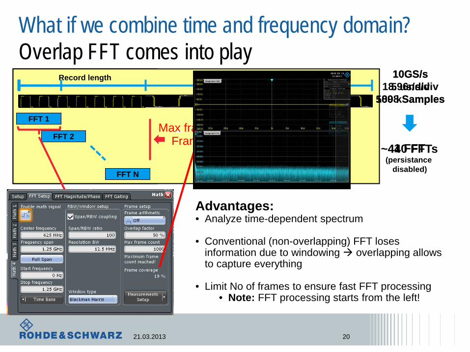
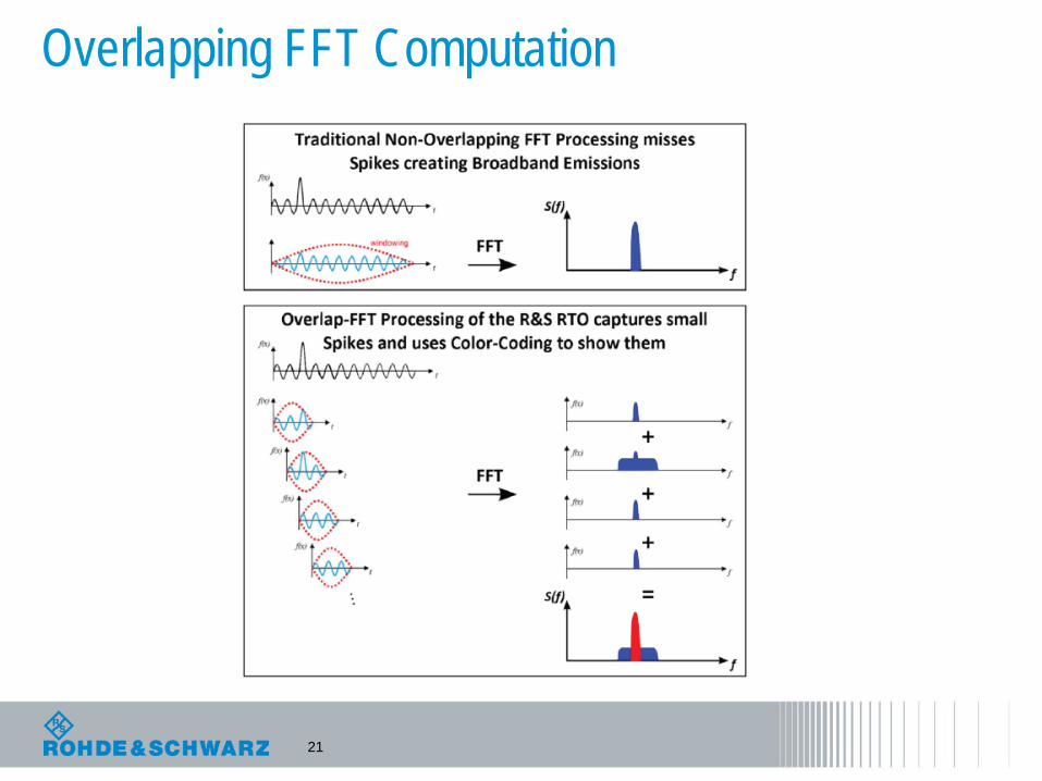
What if we combine time and frequency domain? Overlap FFT comes into play
Advantages: • Analyze time-dependent spectrum
• Conventional (non-overlapping) FFT loses
information due to windowing overlapping allows to capture everything
• Limit No of frames to ensure fast FFT processing • Note: FFT processing starts from the left!
FFT 1
FFT 2
FFT N
Record length
21.03.2013 20
Max frame count limit N = Nmax Frame coverage up to here
10GS/s 18.96ns/div
1898 Samples
1 FFT (persistance
disabled)
10GS/s 5 us/div
500 kSamples
~440 FFTs
21
Overlapping FFT Computation
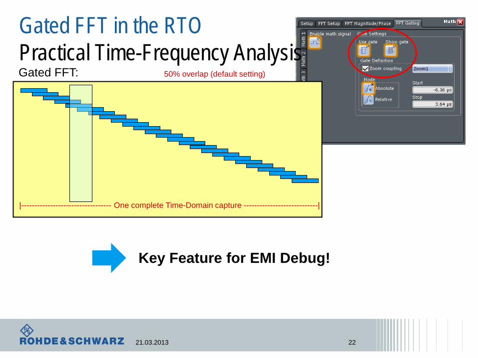
Gated FFT in the RTO Practical Time-Frequency Analysis
50% overlap (default setting) Gated FFT:
|---------------------------------- One complete Time-Domain capture ----------------------------|
Key Feature for EMI Debug!
21.03.2013 22
23
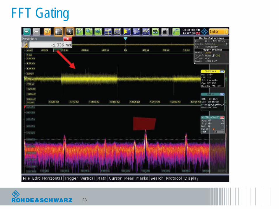
FFT Gating
24
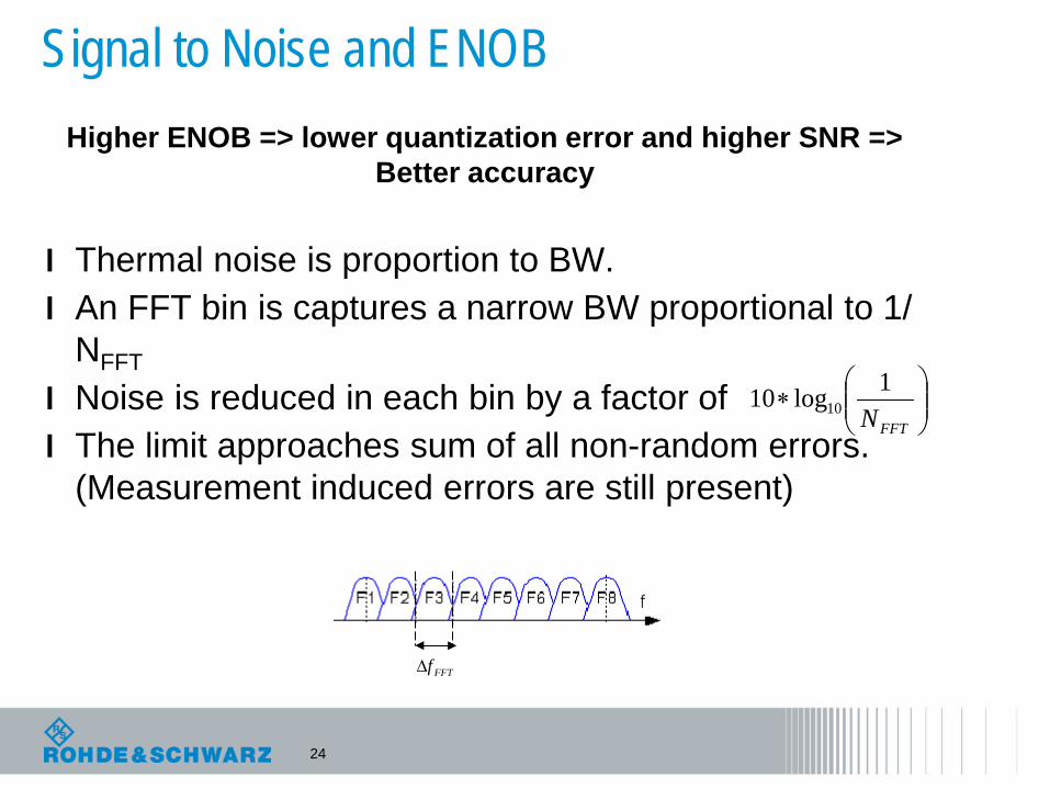
Signal to Noise and ENOB Higher ENOB => lower quantization error and higher SNR =>
Better accuracy
l Thermal noise is proportion to BW. l An FFT bin is captures a narrow BW proportional to 1/
NFFT
l Noise is reduced in each bin by a factor of l The limit approaches sum of all non-random errors.
(Measurement induced errors are still present)
FFTf∆
∗
FFTN1log10 10
25
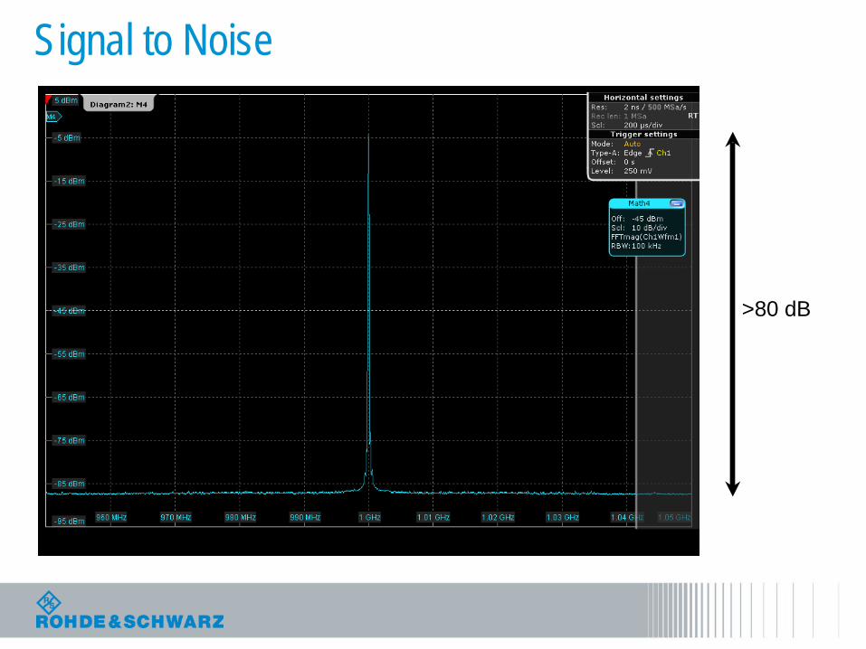
Signal to Noise
>80 dB
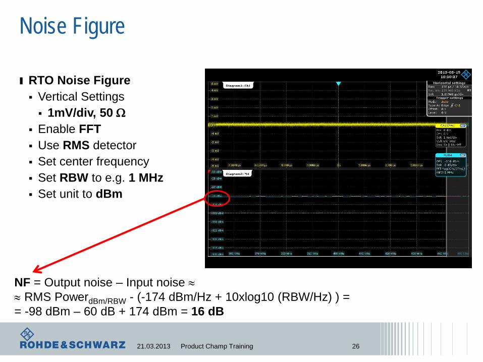
Noise Figure
ı RTO Noise Figure Vertical Settings 1mV/div, 50 Ω
Enable FFT Use RMS detector Set center frequency Set RBW to e.g. 1 MHz Set unit to dBm
21.03.2013 Product Champ Training 26
NF = Output noise – Input noise ≈ ≈ RMS PowerdBm/RBW - (-174 dBm/Hz + 10xlog10 (RBW/Hz) ) = = -98 dBm – 60 dB + 174 dBm = 16 dB
27
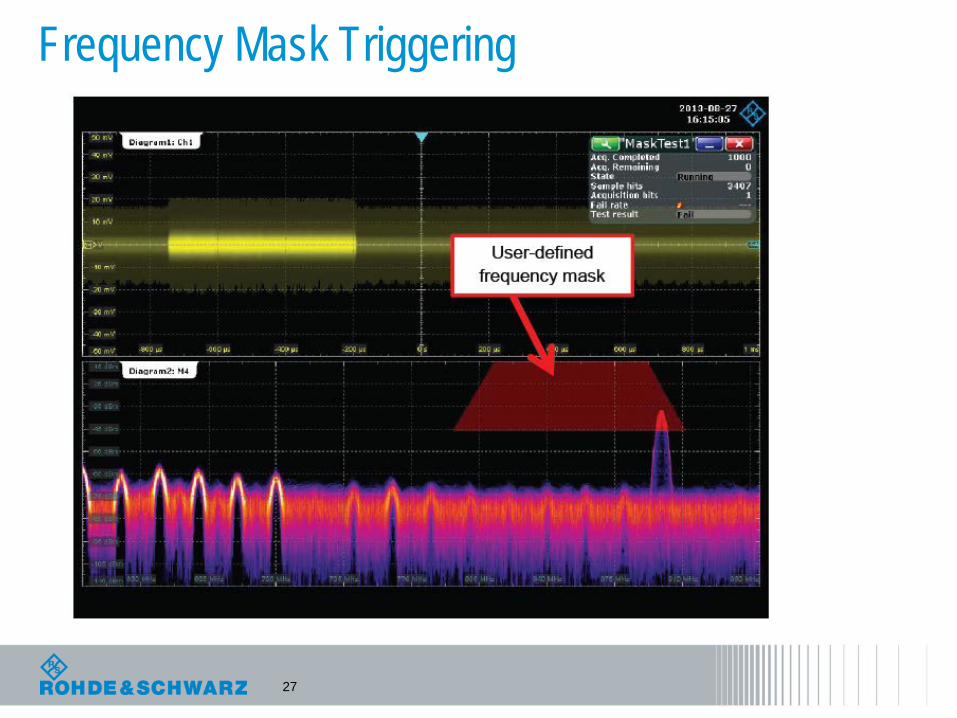
Frequency Mask Triggering
28
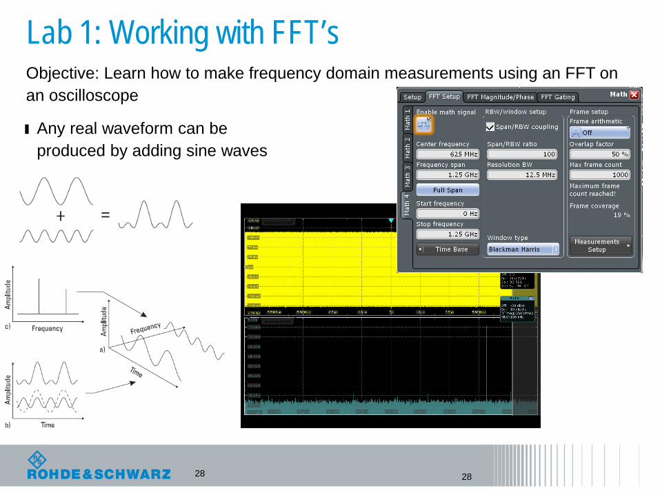
Objective: Learn how to make frequency domain measurements using an FFT on an oscilloscope
Lab 1: Working with FFT’s
28
ı Any real waveform can be produced by adding sine waves
29
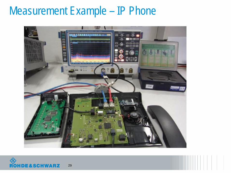
Measurement Example – IP Phone
30
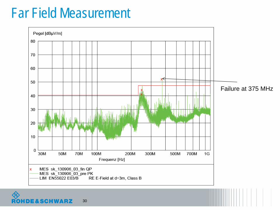
Far Field Measurement
Failure at 375 MHz
31
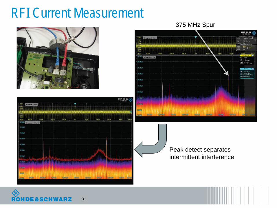
RFI Current Measurement 375 MHz Spur
Peak detect separates intermittent interference
32
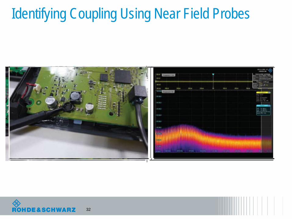
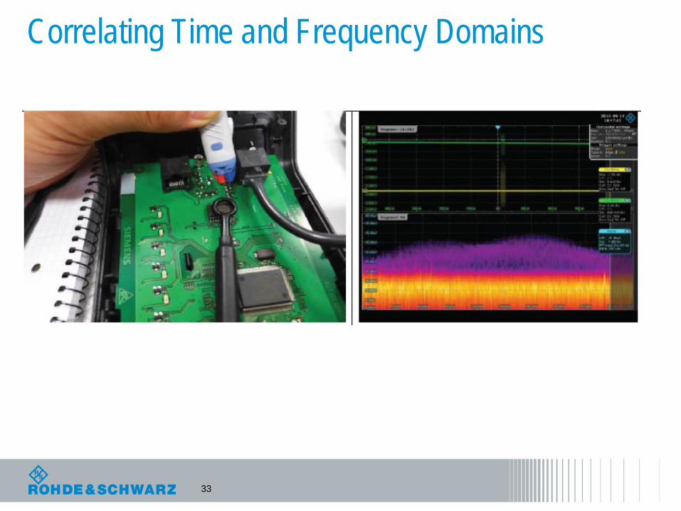
Identifying Coupling Using Near Field Probes
33
Correlating Time and Frequency Domains
Debugging EMI Using a Digital Oscilloscope Summary ı The modern oscilloscope with hardware DDC and overlapping FFT is capable of
far more than a traditional oscilloscope
ı EMI Debugging with an Oscilloscope enables correlation of interfering signals with time domain while maintaining very fast and lively update rate.
ı The combination of synchronized time and frequency domain analysis with advanced triggers allows engineers to gain insight on EMI problems to isolate and converge the solution quickly.
ı Power Supply design choices have a large impact on EMI emissions, frequency and time techniques can help unravel the mystery.
34
Recommended