Copyright © Siemens AG 2010. All rights reserved. 1 ERTEC 200 Data Sheet Technical data subject to change. Version 1.1.2
.
ERTEC 200 Enhanced Real-Time Ethernet Controller
DATA SHEET
Features
Integrated ARM946ES processor Adjustable frequency 50/100/150 MHz 4 Kbytes of data cache 8 Kbytes of instruction cache 4 Kbytes of D-TCM Memory Protection Unit (MPU) Trace functionality, debugging capability via embedded
ICE Interrupt controller IRQ/FIQ
Bus structure
Internal 32-bit bus structure (multilayer bus) with 50 MHz clock pulse frequency
8/16/32-bit bus interface for access to external memory or I/O
General functions
Internal clock pulse generation through PLL Boot ROM with 8 Kbytes Opcode for downloading
firmware from different sources
Test functions Boundary scan
Operating conditions Temperature range: -40 to + 85°C Supply voltage for core: 1.5 V +/- 10% Supply voltage for I/O: 3.3 V +/- 10% Power consumption ( max.):
0,80 W at 1.5 V 0,77 W at 3.3 V
2-Port Switch Two Fast Ethernet ports with integrated PHYs 100 Mbps full duplex Auto-negotiation/auto-crossing/auto-polarity 64 Kbytes of communication RAM Supports PROFINET RT and IRT
External memory interface (EMIF)
Memory controller for SDRAM, 16- or 32-bit Memory controller, 4 x 16 Mbytes for asynchronous
blocks (8-, 16-, or 32-bit data width for SRAM, Flash, external I/O)
Local bus unit (LBU), 16-bit data interface
External host interface for access to the ERTEC 200 16-bit data width Dedicated slave interface
I/O interfaces
45 GPIOs 1 UARTs corresponding to standard UART 16C550 SPI interface (master/slave) 2 timers, 32-bit count down 1 timer, 16-bit count up F-timer, 32-bit count down 2 watchdog functions DMA controller, 1-channel
Package
304-pin plastic FBGA Size, 19 mm x 19 mm 0.8 mm ball pitch
Copyright © Siemens AG 2010. All rights reserved. 2 ERTEC 200 Data Sheet Technical data subject to change. Version 1.1.2
Disclaimer of Liability We have checked the contents of this manual for agreement with the hardware and software described. Since deviations cannot be precluded entirely, we cannot guarantee full agreement. However, the data in this manual are reviewed regularly. Necessary corrections are included in subsequent editions. Suggestions for improvement are welcomed. Copyright © Siemens AG 2008. All rights reserved The reproduction, transmission or use of this document or its contents is not permitted without express written authority. Offenders will be liable for damages. All rights, including rights created by patent grant or registration of a utility model or design, are reserved. All product and system names are registered trademarks of their respective owner and must be treated as such. Technical data subject to change.
Additional Support If you have questions regarding use of the described block that are not addressed in the documentation, please contact your Siemens representative.
Please send your written questions, comments, and suggestions regarding the data sheet to the hotline via the e-mail address indicated above.
In addition, you can receive general information, current product information, FAQs, and downloads pertaining to your application on the Internet at:
http://www.siemens.com/comdec
Technical Contacts for Germany / Worldwide
Siemens AG Automation & Drives ComDeC
Phone: 0911/750-2736 Phone: 0911/750-2080 Fax: 0911/750-2100 E-mail: [email protected]
Street address: Würzburgerstr.121 90766 Fürth Federal Republic of Germany
Mailing address: P.O. Box 2355 90713 Fürth Federal Republic of Germany
Technical Contacts for USA PROFI Interface Center: One Internet Plaza PO Box 4991 Johnson City, TN 37602-4991
Fax: (423)- 262- 2103 Phone: (423)- 262- 2576 E-mail: [email protected]

Copyright © Siemens AG 2010. All rights reserved. 3 ERTEC 200 Data Sheet Technical data subject to change. Version 1.1.2
Contents Description........................................................................................................................................5 ERTEC 200 Function Block Diagram..............................................................................................5 Function Blocks................................................................................................................................6
ARM946ES Processor ..................................................................................................................6 2-Port Switch .................................................................................................................................6 External Memory Interface (EMIF) ................................................................................................7 Local Bus Unit (LBU).....................................................................................................................7 DMA Controller ..............................................................................................................................7 I/O Interface...................................................................................................................................8
45-bit General Purpose I/O (GPIO)..........................................................................................8 UART........................................................................................................................................8 SPI............................................................................................................................................8 Timer T0/T1.............................................................................................................................8 Timer T2 ...................................................................................................................................8 F-timer ......................................................................................................................................9 Watchdog .................................................................................................................................9
Other Functions.............................................................................................................................9 Clock Generation......................................................................................................................9 Reset Logic ..............................................................................................................................9 Boot ROM.................................................................................................................................9 Setting the Operating Mode .....................................................................................................10
Test Functions...............................................................................................................................10 Memory Mapping ..............................................................................................................................11 Detailed Address Mapping ..............................................................................................................12 Package .............................................................................................................................................14 Signal Function Description............................................................................................................15
GPIO 0 to 31 and Alternative Functions........................................................................................15 JTAG and Debug...........................................................................................................................16 Trace Port......................................................................................................................................16 Clock and Reset ............................................................................................................................17 Test Pins........................................................................................................................................17 EMIF (External Memory Interface) ................................................................................................17 LBU, PHY Debug or ETM Trace Interface ....................................................................................19 Ethernet PHY1 and PHY2.............................................................................................................21 Power Supply ................................................................................................................................22
Standard and Alternative Signal Groups .......................................................................................24 Operating/Limit Values and Characteristic Data...........................................................................26
Maximum Limit Values ..................................................................................................................26 Package – Thermal Specification..................................................................................................26 DC Operating Values ....................................................................................................................27 Characteristic Data of Output Drivers ...........................................................................................28 I/O Specification ............................................................................................................................32
LBU-Timing .......................................................................................................................................35 LBU Read from ERTEC 200 with separate Read/Write line (LBU_RDY_N active low) ...............35 LBU Write to ERTEC 200 with separate Read/Write line (LBU_RDY_N active low)....................36 LBU Read from ERTEC 200 with common Read/Write line (LBU_RDY_N active low)................37 LBU Write to ERTEC 200 with common Read/Write line (LBU_RDY_N active low) ....................38
SPI timing specifications.................................................................................................................39 SPI interface configured to slave mode ........................................................................................39 SPI interface configured to master mode......................................................................................40
Timing................................................................................................................................................41 Power-Up Sequence .....................................................................................................................41 Reset .............................................................................................................................................41

Copyright © Siemens AG 2010. All rights reserved. 4 ERTEC 200 Data Sheet Technical data subject to change. Version 1.1.2
List of Figures
Figure 1: ERTEC 200 Block Diagram ...................................................................................................................... 5 Figure 2: ERTEC 200 Package Description .......................................................................................................... 14 Figure 3: LBU-Read-Sequence with separate RD/WR line ................................................................................... 35 Figure 4: LBU-Write-Sequence with separate RD/WR line.................................................................................... 36 Figure 5: LBU-Read-Sequence with common RD/WR line.................................................................................... 37 Figure 6: LBU-Write-Sequenz with common RD-/WR line..................................................................................... 38 Figure 7: SPI Timing in Slave Mode (TI-format Example) ..................................................................................... 39 Figure 8: SPI Timing in Master Mode (TI-format Example) ................................................................................... 40 Figure 9: Reset Timing .......................................................................................................................................... 41 Figure 10: Reset Timing Diagram.......................................................................................................................... 41
List of Tables Table 1: Selection of Download Source................................................................................................................... 9 Table 2: Operating Mode for ERTEC 200.............................................................................................................. 10 Table 3: AHB Masters with Memory Segments Used............................................................................................ 11 Table 4: Overview of AHB Master-Slave Access................................................................................................... 11 Table 5: Detailed Structure of Memory Segments ................................................................................................. 13 Table 6: ERTEC 200 Pin Assignment and Signal Description............................................................................... 22 Table 7: Standard and Alternative Signal Groups.................................................................................................. 25 Table 8: Voltage Supply ........................................................................................................................................ 25 Table 9: Characteristic Data for Operating Values and Limit Values ..................................................................... 26 Table 10: Characteristic Data for Package – Thermal Resistance ........................................................................ 26 Table 11: Characteristic Data of DC Operating Values ......................................................................................... 27 Table 12: Characteristic Data of Output Drivers .................................................................................................... 29 Table 13: Characteristic Data of Input/Clock ......................................................................................................... 30 Table 14: I/O Specification .................................................................................................................................... 33 Table 15: LBU read access timing with seperate Read/Write line ......................................................................... 35 Table 16: LBU write access timing with seperate Read/Write line......................................................................... 36 Table 17: LBU read access timing with common Read/Write line ......................................................................... 37 Table 18: LBU write access timing with common Read/Write line ......................................................................... 38 Table 19: SPI Timing Specifications (slave mode) ................................................................................................ 39 Table 20: SPI Timing Specifications (master mode).............................................................................................. 40

Copyright © Siemens AG 2010. All rights reserved. 5 ERTEC 200 Data Sheet Technical data subject to change. Version 1.1.2
Description
The ERTEC 200 is a powerful, low-cost Ethernet controller for development of PROFINET IO devices. The ERTEC 200 contains a 32-bit processor, external memory interface, local bus unit, Ethernet interface with integrated PHYs, serial ports, DMA controller, and general purpose I/O. Its robust construction, specific automation functions, and openness to the IT world are distinguishing features. The ERTEC 200 is housed in a 304-pin plastic FBGA package (19 mm x 19 mm). The following applications are possible with the ERTEC 200:
Interface for highly accurate drive control Distributed I/O with real-time Ethernet interfacing PROFINET RT and IRT functionality
ERTEC 200 Function Block Diagram
Figure 1: ERTEC 200 Block Diagram
DMA-Controller
AHB/APB Bridge
GPIOM
aste
r
Master
P
P
o
r
t
s
7
APB 50MHz / 32 Bit
74
LBU / MII + SMI / ETM / GPIO
1 x UART
SPI1Interface
3 x Timer,Watchdog,
F-Timer
ARM
9 cl
ock
50M
Hz
100M
Hz
11
25MHz
SC-Bus (50MHz) 32 Bit
2-Port Switch
Switch Control K-SRAM64 kByte
Ethernet-Kanal(Port 1)
Ethernet-Kanal(Port 2)
2120
32
5
GPIO,UART, SPI,Timer,Watchdog,
PHY2
AHB-Wrapper
Slave
Master
Sla
ve
Slav
e
2
Slav
e
Boot-ROM
(8 kByte)
Slav
e
32
8
1
Test
Multi-Layer-AHB50 MHz/32Bit
Memory-Controller
(EMIF)
Slave
InputstageMUX/Arb.
MUX/Arb.
MU
X/Ar
b.
4
Reset
SystemControl
Clock-Unit
F_CLK
48
LocalBus Unit
16 Bit(LBU)
Master
Input stage
MUX
ERTEC200
MC-PLL SignalsPHY
(Port 1)PHY
(Port 2)
ARM946ESwith
I-Cache (8kByte),D-Cache (4kByte),D-TCM (4kByte)
Master
7
BS-TAP
JTAG / Debug
AHB-Wrapper
Master
MC-Bus (50MHz)32 Bit
Slave
Inputstage
ARM-Interrupt-Controller
Slave
DecodeInput stage
Slave
Decode
1
MII-0MII-1
PLL
48
SMI
316
16
ExternalMemory Interface
PHY1
1
REF_CLK
ETM Interface
TRACE_CLK
14
1
13
13
Sla
veSl
ave
Slav
e

Copyright © Siemens AG 2010. All rights reserved. 6 ERTEC 200 Data Sheet Technical data subject to change. Version 1.1.2
Function Blocks
ARM946ES Processor
Adjustable operating frequency, 50/100/150 MHz System control coprocessor (CP15) Data-Tightly Coupled Memory D-TCM, 4 Kbytes Instruction cache with lock functionality, 8 Kbytes Data cache with lock functionality, 4 Kbytes Memory Protection Unit
- Cache enabling for regions - Use of “Write buffer” - Read/write access rights for certain modes only
2 interrupt controllers - IRQ interrupt controller with 16 inputs - FIQ interrupt controller with 8 inputs
Debug functionality by means of JTAG interface Trace functionality by means of the integrated ARM-ETM9 module
- Tracing in full rate mode at an operating frequency of 50/100 MHz - Tracing in half-rate mode at an operating frequency of 150 MHz - Standard mode (no multiplexed or demultiplexed mode) - 4/8-bit data width can be assigned - ETM0 trace macro cells, “medium“ type
4 address comparator pairs 2 data comparators with filter functions 1 trigger input (available externally via GPIO) 1 trigger output (available externally via GPIO) 8 MMD regions for decoding out the physical address space of ERTEC 200 1 sequencer 2 counters
2-Port Switch
2 Fast Ethernet ports with integrated PHYs 100 Mbps full duplex Supports RT and IRT data traffic Auto-negotiation Auto-crossing Auto-polarity Broadcast filter Supports 100Base-TX and 100BASE-FX IEEE 1588 time stamping 64 Kbytes of communication RAM

Copyright © Siemens AG 2010. All rights reserved. 7 ERTEC 200 Data Sheet Technical data subject to change. Version 1.1.2
External Memory Interface (EMIF)
An “external memory interface“ (EMIF) is integrated for access to external memories and I/O. The external memory interface contains the following controllers: SDRAM memory controller
Adjustable 16- or 32-bit data bus width (in the case of 16 bits, the lower 16 data bits are used) PC100 SDRAM-compatible (50 MHz clock frequency) 1 bank with a maximum of 128 MB/32-bit data bus width (2 banks with 64 Mbytes each or 4 banks with
32 Mbytes each). Adjustable RAS/CAS latency (Trcd) (numbers 2, 3 for Write; numbers 1, 2 for Read) No support of auto-precharge command by SDRAM controller SDRAM support
• CAS latency of 2 or 3 clock cycles • 2-bit bank address (1/2/4 banks) via address bits A1 and A0 • 8/9/10/11-bit column address A13, A11:2 • Maximum 13-bit row address A14:2
Asynchronous memory controller for SRAM, Flash, I/O Adjustable 8/16/32-bit data bus width 4 chip select outputs Timing and response to READY can be set individually for each chip select Synchronous or asynchronous READY can be set individually for each chip select Default setting is “slow timing” for BOOT operation Maximum of 16 Mbytes can be addressed for each chip select Chip select CS_PER0_N is bootable Data bus width of boot ROM at CS_PER0_N is detected via BOOT[3:0] pins. Adjustable timeout monitoring DTXR (direction) and OE_DRIVER_N (enable) control signals for direct control of an external driver to
signals CS_PER0_N – CS_PER3_N
Local Bus Unit (LBU)
An external host can be connected to the ERTEC 200 via the local bus unit. The LBU has the following features:
16-bit data bus width Host access to LBU paging registers via chip select signal LBU_CS_R_N Host access to any address area of ERTEC 200 via chip select signal LBU_CS_M_N Maximum of 4 pages can be addressed Adjustable page-range and page-offset for each page; reconfigurable at any time
DMA Controller
1-channel DMA controller 4 request inputs for synchronization with the I/O (SPI or UART) Change address mode/Hold address mode can be set 8-, 16-, or 32-bit data bus width can be set Control of DMA transfer via a hardware signal or software control is possible End of DMA transfer is indicated by an interrupt The following DMA transfers are supported:
Internal memory external memory (SRAM/SDRAM EMIF memory) Internal memory I/O (UART or SPI)

Copyright © Siemens AG 2010. All rights reserved. 8 ERTEC 200 Data Sheet Technical data subject to change. Version 1.1.2
I/O Interface
All I/O are connected to the 32-bit APB I/O bus. All I/O blocks are operated as a slave with a low performance requirement. The following I/O interfaces are implemented in the ERTEC 200.
45-bit General Purpose I/O (GPIO)
GPIO 0 to 31 can be assigned for up to 4 different functions (see Signal Function Description) GPIO 32 to 44 can be used as an alternative function for the LBU interface (setting via configuration
pins) Input/outputs can be assigned on a bit-by-bit basis All GPIO equipped with internal pull-up 4 GPIO inputs have interrupt capability (active Low level is not supported as an interrupt level) 8-, 16-, or 32-bit access to registers is possible
UART
The UART is similar to the standard UART 16C550. The UART differs from the standard UART 16C550 as follows:
Receive FIFO trigger level is set permanently to 8. Receive errors are stored in the FIFO and do not generate an interrupt The internal register address mapping and the register bit functions are different Only 1 or 2 Stop bits are supported No “forcing stick parity function” Control via DMA controller is possible Baud rate of 110 baud to 115.2 Kbaud can be assigned
SPI
The integrated SPI supports the following modes: o Motorola-compatible SPI mode o Texas Instruments synchronous serial interface o National Instruments Microwire interface Features:
Programmable 4- to 16-bit data frame size Programmable bit rate
* 769 Hz to 25 MHz at a base frequency of 50 MHz as master * Maximum of 4.16 MHz as slave
Send and Receive FIFO with 8 16-bit entries Group and overrun error interrupt on the ARM interrupt controller
Timer T0/T1
32-bit down counter Load/reload-capable Start, stop, and continue functions Interrupts can be generated by Timer 0 and Timer 1 Both timers can be cascaded to a 64-bit timer Read/write accessible count register 50 MHz input clock (default) or 8-bit prescaler per timer can be assigned
Timer T2
16-bit count up Load/reload-capable Start and stop functions Interrupts can be generated by Timer 2 50 MHz clock frequency One-shot mode, cycle mode, and retrigger mode can be assigned

Copyright © Siemens AG 2010. All rights reserved. 9 ERTEC 200 Data Sheet Technical data subject to change. Version 1.1.2
F-timer
External input clock “Byp_Clk” 32-bit count down Edge-triggered
Watchdog
Watchdog 0: 32-bit count-down with output pin WDOUT0_N Watchdog 1: 36-bit count-down (bits 0 to 3 are not used) Load/reload function Write protection for watchdog Watchdog interrupt on the ARM-FIQ interrupt controller
Other Functions
Clock Generation
The required clocks of the ERTEC 200 are made available by means of internal PLL and/or through direct infeed. The PLL is fed with a 12.5 MHz clock signal; alternatively, the clock signal can be supplied via quartz circuitry or an oscillator infeed. JTAG and MII MAC/PHYs have a direct clock supply.
ARM946ES 50/100/150 MHZ (PLL) AHB/EMIF/ICU 50 MHz (PLL) IRT 50/100/150 MHZ (PLL) APB 50 MHz (PLL) JTAG 0 .. 10 MHz (JTAG clock)
Reset Logic
The ERTEC 200 offers several options for triggering a RESET. The triggering event can be read out from a “reset status register“ in the system control register area. The following RESET options are available:
Hardware reset Watchdog reset Software reset
Boot ROM
The boot ROM is organized as a 2 Kbyte x 32-bit (8 Kbytes) memory. It contains the opcode for downloading firmware from various I/O. The download sources are selected by reading in the BOOT [3:0] pins while HW reset RESET_N is active. The following download sources are available:
BOOT[3] BOOT[2] BOOT[1] BOOT[0] BOOTING OF 0 0 0 0 External ROM with 8-bit data width 0 0 0 1 External ROM with 16-bit data width 0 0 1 0 External ROM with 32-bit data width 1 0 0 0 Fast External ROM with 8-bit data width 1 0 0 1 Fast External ROM with 16-bit data width 1 0 1 0 Fast External ROM with 32-bit data width 0 0 1 1 Reserved 0 1 0 0 Reserved 0 1 0 1 SPI1 0 1 1 0 UART 0 1 1 1 LBU 1 0 1 1 Reserved
Table 1: Selection of Download Source

Copyright © Siemens AG 2010. All rights reserved. 10 ERTEC 200 Data Sheet Technical data subject to change. Version 1.1.2
Notice!! Pull-up/pull-down resistors on the BOOT pins are needed to set the boot modes. Setting the Operating Mode
The operating and testing modes are set by reading in the CONFIG[6 : 1] pins while HW reset RESET_N is active. The following operating modes can be set:
CONFIG [1] Meaning 1 REF_CLK tristate 0 REF_CLK output (25 MHz)
CONFIG [4]
CONFIG [3] Meaning
0 0 ARM clock 50 MHz 0 1 ARM clock 100 MHz 1 0 ARM clock 150 MHz 1 1 Reserved
CONFIG [6]
CONFIG [5]
CONFIG [2] Meaning
X 1 0 LBU = On 1 LBU-CFG: LBU_WR_N has
read/write control
X 0 0 LBU = On, LBU-CFG: Separate read and write line
1 X 0 LBU = On, LBU_POL_RDY: LBU_RDY_N is high-active
0 X 0 LBU = On,
LBU_POL_RDY: LBU_RDY_N is low-active
0 1 1 LBU = Off,
GPIO44-32 = On, int. PHYs = On, External MII = PHY debugging, ETM9 = Off
1 0 1 LBU = Off,
GPIO44-32 = On, int. PHYs = On, External MII = Off, ETM9 = On
1 1 1
Reserved
Table 2: Operating Mode for ERTEC 200
Notice!! Pull-up/pull-down resistors on the CONFIG pins are needed to set the configuration modes. x = don’t care
Test Functions
Boundary scan The TAP_SEL input on the ERTEC 200 is used to enable and disable the boundary scan (see Signal Function Description).
1 GPIO44-32 = Off, int. PHYs = On, ext. MII = Off, ETM9 = Off

Copyright © Siemens AG 2010. All rights reserved. 11 ERTEC 200 Data Sheet Technical data subject to change. Version 1.1.2
Memory Mapping
The four AHB masters (ARM946, switch, LBU, and DMA) of the ERTEC 200 use the memory area differently. The table below presents the AHB masters and the memory segments used.
Start and End
Address Seg. Function Area for
ARM9 Function Area for
Switch Function Area for
LBU Function Area for
DMA
0000 0000
0FFF FFFF
0
Boot ROM (0-8 Kbytes)
EMIF-SDRAM (0-128 Mbytes) EMIF memory (0-64 Mbytes)
D-TCM (4 Kbytes)locked I-cache (2/4/6 Kbytes)
Boot ROM (0-8 Kbytes)
EMIF-SDRAM (0-128 Mbytes) EMIF memory (0-64 Mbytes)
Boot ROM (0-8 Kbytes)
EMIF-SDRAM (0-128 Mbytes) EMIF memory (0-64 Mbytes
Boot ROM (0-8 Kbytes)
EMIF-SDRAM (0-128 Mbytes) EMIF memory (0-64 Mbytes
1000 0000
1FFF FFFF 1 Switch controller Switch controller Switch controller Not used
2000 0000
2FFF FFFF 2 EMIF (SDRAM) EMIF (SDRAM) EMIF (SDRAM) EMIF (SDRAM)
3000 0000
3FFF FFFF 3 EMIF (Area: Bank
0-3) EMIF (Area: Bank
0-3) EMIF (Area: Bank
0-3) EMIF (Area: Bank
0-3)
4000 0000
4FFF FFFF 4 All APB macros
incl. boot ROM Not used All APB macros incl. boot ROM
All APB macros incl. boot ROM
5000 0000
5FFF FFFF 5 ARM-ICU Not used Not used Not used
6000 0000
6FFF FFFF 6 Not used Not used Not used Not used
7000 0000
7FFF FFFF 7 EMIF register Not used EMIF register Not used
8000 0000
8FFF FFFF 8 DMA Not used Not used Not used
9000 0000 FFFF FFFF
9 - 15 Not used Not used Not used Not used
Table 3: AHB Masters with Memory Segments Used
The table below shows which AHB masters can communicate with which AHB slaves.
AHB Master-Slave Coupling Slave
Master
APB Slave 1
EMIF Slave 2
DMA Slave 3
Switch Slave 4
INT Control Slave 5
ARM X X X X X Switch X
DMA X X
LBU X X X
Table 4: Overview of AHB Master-Slave Access

Copyright © Siemens AG 2010. All rights reserved. 12 ERTEC 200 Data Sheet Technical data subject to change. Version 1.1.2
Detailed Address Mapping
The following table shows the detailed partitioning of the individual memory segments. Mirrored segments should not be used for addressing to ensure compatible memory expansion at a later date.
Segment Contents Size Address Area Description
0
Boot ROM (0 - 8 Kbytes) or
EMIF SDRAM (0-128 Mbytes)
or EMIF memory (0-64
Mbytes) or
Locked I-cache (2/4/6 Kbytes)
256 Mbytes 0000_0000 - 0FFF_FFFF
After reset: Boot ROM (8 Kbytes, physical;
Memory swap=00b); After memory swap:
EMIFSDRAM (128 Mbytes, physical; Memory swap=01b);
or EMIF memory (64 Mbytes physical;
Memory swap=10b); From ARM9 perspective, the locked I-
cache (2/4/6 Kbytes) or a D-TCM (4 Kbytes) can be displayed.
Note2
1 Switch 256 MB 1000_0000 - 1FFF_FFFF
2 Mbytes, physical; 27 * imaged; - 0-1 MByte for switch register - 1-2 Mbytes for KRAM
Note1
2 EMIF (SDRAM) 256 Mbytes 2000_0000 - 2FFF_FFFF
128 Mbytes When a smaller memory area is used,
mirroring over the entire area Note2
3 EMIF I/O Bank 0 16 Mbytes 3000_0000 -
30FF_FFFF When a smaller device is interfaced, mirroring
over the entire 16 Mbytes
EMIF I/O Bank 1 16 Mbytes 3100_0000 -
31FF_FFFF When a smaller device is interfaced, mirroring
over the entire 16 Mbytes
EMIF I/O Bank 2 16 Mbytes 3200_0000 -
32FF_FFFF When a smaller device is interfaced, mirroring
over the entire 16 Mbytes
EMIF I/O Bank 3 16 Mbytes 3300_0000 -
33FF_FFFF When a smaller device is interfaced, mirroring
over the entire 16 Mbytes
Not used 3400_0000 - 3FFF_FFFF
4 Internal boot ROM 8 Kbytes 4000_0000- 4000_1FFF 8 Kbytes, physical
Timer 0 - 2 256 bytes 4000_2000 - 4000_20FF
32 bytes, physical Note2
Watchdog 256 bytes 4000_2100 - 4000_21FF
28 bytes, physical Note2
SPI 256 bytes 4000_2200 - 4000_22FF 256 bytes, physical
UART1 256 bytes 4000_2300 - 4000_23FF 256 bytes, physical
GPIO 256 bytes 4000_2500 - 4000_25FF
32 bytes, physical Note2
System control register block 256 bytes 4000_2600 -
4000_26FF
164 bytes, physical System register block of ERTEC 200
Note2
F-counter 256 bytes 4000_2700 - 4000_27FF
8 bytes, physical Note2

Copyright © Siemens AG 2010. All rights reserved. 13 ERTEC 200 Data Sheet Technical data subject to change. Version 1.1.2
Segment Contents Size Address Area Description
Not used 4000_2800- 4000_FFFF
Not used 4001_2800-4FFF_FFFF
5 ARM-ICU 256 Mbytes 5000_0000- 5FFF_FFFF
ARM - Interrupt controller 256 bytes, physical
Note2
6 Not used 256 Mbytes 6000_0000- 6FFF_FFFF
7 EMIF register 256 Mbytes 7000_0000- 7FFF_FFFF
Control register for external memory interface
1 Mbyte, physical Note2
8 DMA register 256 Mbytes 8000_0000- FFFF_FFFF
DMA controller 32 bytes, physical
Note2
9 - 15 Not used 1.75 Gbyte 9000_0000- FFFF_FFFF
Table 5: Detailed Structure of Memory Segments
If the "Locked I-cache” and “D-TCM” memories are used, they appear only from the point of view of the ARM processor and not the LBU, switch or DMA controllers. Note: 1. Access to IRT registers and KRAM should only occur in the address areas indicated above (first 2 Mbytes). An access to areas within the 2 Mbytes that are not occupied by the IRT registers and KRAM result in undefined access (acknowledgement timeout). The read or written data are not valid. While the 2-Mbyte areas are mirrored within the 8-Mbyte physical address area, different access types are used:
2-4-Mbyte area for unaligned consistent 16-bit accesses to IRT 4-6-Mbyte area for unaligned consistent 32-bit accesses to IRT 6-8 Mbytes is not supported (supplies undefined values)
The 8-Mbyte address area is mirrored 32 times within the 256 Mbytes. 2. Memory areas are mirrored according to the following formula: Memory size N = -------------------------------------------- Physical memory size Physical memory size is limited to values of 2n (2, 4, 8, ... 128, 256 etc.) Example: The physical memory size of the watchdog is 28 bytes. However, 32 bytes are taken for calculating the number of mirrorings N. In this case, the number of mirrorings N = 8. Access to the 4 unused bytes does not result in an acknowledgement timeout, but the read or written values are undefined.

Copyright © Siemens AG 2010. All rights reserved. 14 ERTEC 200 Data Sheet Technical data subject to change. Version 1.1.2
Package
The ERTEC 200 is supplied in a 304-pin FBGA package. The distance between the pins is 0.8 mm. The package dimensions are 19 mm x 19 mm.
Figure 2: ERTEC 200 Package Description When working with modules, always take precautionary measures against electrostatic charge (ESD – Electrostatic Sensitive Devices).
Copyright © Siemens AG 2010. All rights reserved. 15 ERTEC 200 Data Sheet Technical data subject to change. Version 1.1.2
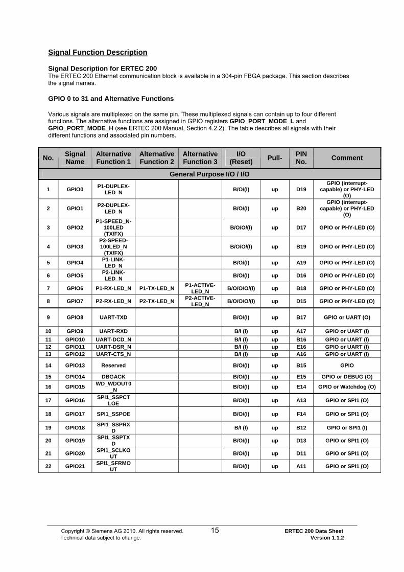
Signal Function Description
Signal Description for ERTEC 200 The ERTEC 200 Ethernet communication block is available in a 304-pin FBGA package. This section describes the signal names.
GPIO 0 to 31 and Alternative Functions
Various signals are multiplexed on the same pin. These multiplexed signals can contain up to four different functions. The alternative functions are assigned in GPIO registers GPIO_PORT_MODE_L and GPIO_PORT_MODE_H (see ERTEC 200 Manual, Section 4.2.2). The table describes all signals with their different functions and associated pin numbers.
No. Signal Name
Alternative Function 1
Alternative Function 2
Alternative Function 3
I/O (Reset) Pull- PIN
No. Comment
General Purpose I/O / I/O
1 GPIO0 P1-DUPLEX-LED_N B/O/(I) up D19
GPIO (interrupt-capable) or PHY-LED
(O)
2 GPIO1 P2-DUPLEX-LED_N B/O/(I) up B20
GPIO (interrupt-capable) or PHY-LED
(O)
3 GPIO2 P1-SPEED_N-
100LED (TX/FX)
B/O/O/(I) up D17 GPIO or PHY-LED (O)
4 GPIO3 P2-SPEED-100LED_N
(TX/FX) B/O/O/(I) up B19 GPIO or PHY-LED (O)
5 GPIO4 P1-LINK-LED_N B/O/(I) up A19 GPIO or PHY-LED (O)
6 GPIO5 P2-LINK-LED_N B/O/(I) up D16 GPIO or PHY-LED (O)
7 GPIO6 P1-RX-LED_N P1-TX-LED_N P1-ACTIVE-LED_N B/O/O/O/(I) up B18 GPIO or PHY-LED (O)
8 GPIO7 P2-RX-LED_N P2-TX-LED_N P2-ACTIVE-LED_N B/O/O/O/(I) up D15 GPIO or PHY-LED (O)
9 GPIO8 UART-TXD B/O/(I) up B17 GPIO or UART (O)
10 GPIO9 UART-RXD B/I (I) up A17 GPIO or UART (I) 11 GPIO10 UART-DCD_N B/I (I) up B16 GPIO or UART (I) 12 GPIO11 UART-DSR_N B/I (I) up E16 GPIO or UART (I) 13 GPIO12 UART-CTS_N B/I (I) up A16 GPIO or UART (I) 14 GPIO13 Reserved B/O/(I) up B15 GPIO 15 GPIO14 DBGACK B/O/(I) up E15 GPIO or DEBUG (O) 16 GPIO15 WD_WDOUT0
_N B/O/(I) up E14 GPIO or Watchdog (O)
17 GPIO16 SPI1_SSPCTLOE B/O/(I) up A13 GPIO or SPI1 (O)
18 GPIO17 SPI1_SSPOE B/O/(I) up F14 GPIO or SPI1 (O)
19 GPIO18 SPI1_SSPRXD B/I (I) up B12 GPIO or SPI1 (I)
20 GPIO19 SPI1_SSPTXD B/O/(I) up D13 GPIO or SPI1 (O)
21 GPIO20 SPI1_SCLKOUT B/O/(I) up D11 GPIO or SPI1 (O)
22 GPIO21 SPI1_SFRMOUT B/O/(I) up A11 GPIO or SPI1 (O)

Copyright © Siemens AG 2010. All rights reserved. 16 ERTEC 200 Data Sheet Technical data subject to change. Version 1.1.2
No. Signal Name
Alternative Function 1
Alternative Function 2
Alternative Function 3
I/O (Reset) Pull- PIN
No. Comment
General Purpose I/O / I/O
23 GPIO22 SPI1_SFRMIN DBGACK B/I/O/(I) up F10
GPIO or SPI1 (I) or Debug (O)
This GPIO is used as chip select when
booting from Nand Flash or SPI ROM.
24 GPIO23 SPI1_SCLKIN Reserved B/I/O/(I) up D10
GPIO or SPI1 (I) This GPIO is used as
chip select when booting from SPI Flash
or SPI EEPROM. 25 GPIO24 PLL_EXT_IN_
N B/I (I) up B11 GPIO or MC_PLL (I)
26 GPIO25 TGEN_OUT1_N *1 B/O/(I) up B9 GPIO or MC_PLL (O)
27 GPIO26 TGEN_OUT2_N B/O/(I) up A7 GPIO or MC_PLL (O)
28 GPIO27 TGEN_OUT3_N B/O/(I) up B10 GPIO or MC_PLL (O)
29 GPIO28 TGEN_OUT4_N B/O/(I) up F9 GPIO or MC_PLL (O)
30 GPIO29 TGEN_OUT5_N B/O/(I) up E9 GPIO or MC_PLL (O)
31 GPIO30 TGEN_OUT6_N B/O/(I) up B8
GPIO (interrupt-capable) or MC_PLL
(O) 32 GPIO31 DBGREQ B/I (I) up E8 GPIO (interrupt-
capable) or DEBUG (I) *1 For an IRT application pin GPIO25 is default parameterized as alternate function1 (TGEN_OUT1_N). A synchronous clock is issued at this pin. During the certification process of a PROFINET IO DEVICE with IRT functionality this pin has to be accessible from outside (mandatory). Different GPIO’s are used on the Evaluation Board EB200. See Dokument „EB 200 Manual” Table 6.
JTAG and Debug
No. Signal Name
I/O (Reset) Pull- PIN
No. Comment
Debug / JTAG (BOUNDARY SCAN) 33 TRST_N I (I) U10 JTAG Reset 34 TCK I (I) up W7 JTAG Clock 35 TDI I (I) up U9 JTAG Data In 36 TMS I (I) up V7 JTAG Test Mode Select 37 TDO O (O) V9 JTAG Data Out 38 SRST_N B (O) up V8 Hardware Reset
39 TAP_SEL I (I) up W8 Select TAP Controller:
0: Boundary Scan TAP Controller selected 1: ARM-TAP Controller selected
or Scan Clock (Scan mode)
Trace Port
No. Signal Name
I/O (Reset) Pull- PIN
No. Comment
Trace Port/Other 40 TRACECLK B (O) AB4 ETM Trace Clock 41 RESERVED I (I) up U19 Connect Pin to Ground

Copyright © Siemens AG 2010. All rights reserved. 17 ERTEC 200 Data Sheet Technical data subject to change. Version 1.1.2
Clock and Reset
No. Signal Name I/O (Reset) Pull- PIN
No. Comment
CLOCK / RESET GENERATION 42 CLKP_A I (I) B14 Quartz connection 43 CLKP_B O (O) D14 Quartz connection 44 F_CLK I (I) B13 F_CLK for F-counter
45 REF_CLK Dependent
on PIN CONFIG[1]
A15 Tristate or reference clock output, 25 MHz
46 RESET_N I (I) up B7 PowerOn reset
Test Pins
No. Signal Name I/O Pull- PIN
No. Comment
TEST 47 TEST_N (3) I up T5 Test mode 48 TMC1 (3) I G5 Test configuration 49 TMC2 (3) I H6 Test configuration 50 TACT_N (3) I dn J5 TESTACT-TAP reset
EMIF (External Memory Interface)
No. Signal Name Alternative Reset Function
I/O (Reset) Pull- PIN
No. Comment
EMIF (External Memory Interface)
51 DTR_N BOOT0 B (I) up E7 Direction signal for external driver
or scan clock (Scan mode) ERTEC 200 boot mode (external
PD may be necessary) 52 OE_DRIVER_N O (O) D8 Enable signal for external driver
or scan clock (Scan mode) 53 A0 O (O) B4 Address bit 0
SDRAM: Bank address 0 54 A1 O (O) A3 Address bit 1
SDRAM: Bank address 1 55 A2 O (O) B3 Address bit 2
SDRAM: Address 0 56 A3 O (O) B2 Address bit 3
SDRAM: Address 1 57 A4 O (O) D4 Address bit 4
SDRAM: Address 2 58 A5 O (O) C2 Address bit 5
SDRAM: Address 3 59 A6 O (O) C1 Address bit 6
SDRAM: Address 4 60 A7 O (O) D2 Address bit 7
SDRAM: Address 5 61 A8 O (O) D1 Address bit 8
SDRAM: Address 6 62 A9 O (O) E2 Address bit 9
SDRAM: Address 7 63 A10 O (O) E1 Address bit 10
SDRAM: Address 8 64 A11 O (O) F2 Address bit 11
SDRAM: Address 9 65 A12 O (O) F1 Address bit 12
SDRAM: Address 10

Copyright © Siemens AG 2010. All rights reserved. 18 ERTEC 200 Data Sheet Technical data subject to change. Version 1.1.2
No. Signal Name Alternative Reset Function
I/O (Reset) Pull- PIN
No. Comment
EMIF (External Memory Interface) 66 A13 O (O) G2 Address bit 13
SDRAM: Address 11 67 A14 O (O) G1 Address bit 14
SDRAM: Address 12
68 A15 BOOT1 (1) B (I) dn H2 Address bit 15
ERTEC 200 boot mode (ext. PU may be necessary)
69 A16 BOOT2 (1) B (I) dn J2 Address bit 16 /
ERTEC 200 boot mode (ext. PU may be necessary)
70 A17 BOOT3 (1) B (I) up K2 Address bit 17 /
ERTEC 200 boot mode (ext. PD may be necessary)
71 A18 CONFIG1 (2) B (I) up K1 Address bit 18 / ERTEC 200
system configuration (external PD may be necessary)
72 A19 CONFIG2 (2) B (I) up E4 Address bit 19 / ERTEC 200
system configuration (external PD may be necessary)
73 A20 CONFIG3 (2) B (I) dn F4 Address bit 20 / ERTEC 200
system configuration (external PU may be necessary)
74 A21 CONFIG4 (2) B (I) up G4 Address bit 21 / ERTEC 200
system configuration (external PD may be necessary)
75 A22 CONFIG5 (2) B (I) dn H5 Address bit 22 / ERTEC 200
system configuration (external PU may be necessary)
76 A23 CONFIG6 (2) B (I) up H4 Address bit 23 / ERTEC 200
system configuration (external PD may be necessary)
77 D0 B (I) up M2 Data bit 0 78 D1 B (I) up N2 Data bit 1 79 D2 B (I) up P1 Data bit 2 80 D3 B (I) up P2 Data bit 3 81 D4 B (I) up R1 Data bit 4 82 D5 B (I) up T2 Data bit 5 83 D6 B (I) up U1 Data bit 6 84 D7 B (I) up U2 Data bit 7 85 D8 B (I) up V2 Data bit 8 86 D9 B (I) up W1 Data bit 9 87 D10 B (I) up W2 Data bit 10 88 D11 B (I) up Y2 Data bit 11 89 D12 B (I) up AA1 Data bit 12 90 D13 B (I) up AA2 Data bit 13 91 D14 B (I) up AB2 Data bit 14 92 D15 B (I) up AA3 Data bit 15 93 D16 B (I) up K4 Data bit 16 94 D17 B (I) up K5 Data bit 17 95 D18 B (I) up J6 Data bit 18 96 D19 B (I) up K6 Data bit 19 97 D20 B (I) up N5 Data bit 20 98 D21 B (I) up N6 Data bit 21 99 D22 B (I) up P6 Data bit 22
100 D23 B (I) up R5 Data bit 23 101 D24 B (I) up R6 Data bit 24 102 D25 B (I) up P4 Data bit 25 103 D26 B (I) up R4 Data bit 26 104 D27 B (I) up T4 Data bit 27 105 D28 B (I) up U4 Data bit 28 106 D29 B (I) up W4 Data bit 29 107 D30 B (I) up W5 Data bit 30 108 D31 B (I) up W6 Data bit 31

Copyright © Siemens AG 2010. All rights reserved. 19 ERTEC 200 Data Sheet Technical data subject to change. Version 1.1.2
No. Signal Name Alternative Reset Function
I/O (Reset) Pull- PIN
No. Comment
EMIF (External Memory Interface) 109 WR_N O (O) A4 Write strobe 110 RD_N O (O) B5 Read strobe 111 CS_PER0_N O (O) D5 Chip Select Bank 1 (ROM);
boot area 112 CS_PER1_N O (O) A5 Chip select bank 2 113 CS_PER2_N O (O) A6 Chip select bank 3 114 CS_PER3_N O (O) B6 Chip select bank 4 115 BE0_DQM0_N O (O) N4 Byte enable 0 for D(7:0) 116 BE1_DQM1_N O (O) V1 Byte enable 1 for D(15:8) 117 BE2_DQM2_N O (O) J4 Byte enable 2 for D(23:16) 118 BE3_DQM3_N O (O) P5 Byte enable 3 for D(31:24) 119 RDY_PER_N I (I) up D7 Ready signal 120 CLK_SDRAM B (O) M1 Clock SDRAM 121 CS_SDRAM_N O (O) L1 Chip select SDRAM 122 RAS_SDRAM_N O (O) M5 RAS SDRAM 123 CAS_SDRAM_N O (O) L2 CAS SDRAM 124 WE_SDRAM_N O (O) M4 RD/WR SDRAM
LBU, PHY Debug or ETM Trace Interface
No.
Function 1 LBU
Config [6,5,2]=xx0b
Function 2 PHY Debug
and GPIO[44:32]
Config [6,5,2]=011b
Function 3 ETM Trace
and GPIO[44:32]
Config [6,5,2]=101b
Function 4
Reserved
[6,5,2]=111b
I/O (Reset
see Config[6,5,2])
Pull-
PIN No. Comment
LBU / MII Interface/ ETM Trace Interface 125 LBU_A0 RXD_P10 ETMEXTOUT I/O/O/I
(ETM : I) up AB3 LBU or MII or ETM
126 LBU_A1 RXD_P11 ETMEXTIN1 I/O/I/I (ETM : I) up AA4 LBU or MII or ETM
127 LBU_A2 RXD_P12 TRACEPKT7 I/O/O/I (ETM : I) up AA5 LBU or MII or ETM
128 LBU_A3 RXD_P13 TRACEPKT6 I/O/O/I (ETM : I) up AB5 LBU or MII or ETM
129 LBU_A4 CRS_P1 TRACEPKT5 I/O/O/I (ETM : I) up AA6 LBU or MII or ETM
130 LBU_A5 RX_ER_P1 TRACEPKT4 I/O/O/I (ETM : I) up AB6 LBU or MII or ETM
131 LBU_A6 RX_DV_P1 TRACEPKT3 I/O/O/I (ETM : I) up AA7 LBU or MII or ETM
132 LBU_A7 COL_P1 TRACEPKT2 I/O/O/I (ETM : I) up AB7 LBU or MII or ETM
133 LBU_A8 RXD_P20 TRACEPKT1 I/O/O/I (ETM : I) up AA8 LBU or MII or ETM
134 LBU_A9 RXD_P21 TRACEPKT0 I/O/O/I (ETM : I) up AB8 LBU or MII or ETM
135 LBU_A10 RXD_P22 TRACESYNC I/O/O/I (ETM : I) up AA9 LBU or MII or ETM
136 LBU_A11 RXD_P23 PIPESTA2 I/O/O/I (ETM : I) up AA10 LBU or MII or ETM
137 LBU_A12 CRS_P2 PIPESTA1 I/O/O/I (ETM : I) up AB10 LBU or MII or ETM
138 LBU_A13 RX_ER_P2 PIPESTA0 I/O/O/I (ETM : I) up AA11 LBU or MII or ETM
139 LBU_A14 RX_DV_P2 I/O/I/I up AB11 LBU or MII
140 LBU_A15 COL_P2 I/O/I/I up W11 LBU or MII

Copyright © Siemens AG 2010. All rights reserved. 20 ERTEC 200 Data Sheet Technical data subject to change. Version 1.1.2
No.
Function 1 LBU
Config [6,5,2]=xx0b
Function 2 PHY Debug
and GPIO[44:32]
Config [6,5,2]=011b
Function 3 ETM Trace
and GPIO[44:32]
Config [6,5,2]=101b
Function 4
Reserved
[6,5,2]=111b
I/O (Reset
see Config[6,5,2])
Pull-
PIN No. Comment
LBU / MII Interface/ ETM Trace Interface 141 LBU_A16 GPIO32 GPIO32 I/B/B/B
(GPIO:I) up W9 LBU or GPIO
142 LBU_A17 GPIO33 GPIO33 I/B/B/B (GPIO:I) up W10 LBU or GPIO
143 LBU_A18 GPIO34 GPIO34 I/B/B/B (GPIO:I) up V10 LBU or GPIO
144 LBU_A19 GPIO35 GPIO35 I/B/B/B (GPIO:I) up W12 LBU or GPIO
145 LBU_A20 GPIO36 GPIO36 I/B/B/B (GPIO:I) up V12 LBU or GPIO
146 LBU_SEG_0 GPIO37 GPIO37 I/B/B/B (GPIO:I) up V13 LBU or GPIO
147 LBU_SEG_1 GPIO38 GPIO38 I/B/B/B (GPIO:I) up U13 LBU or GPIO
148 LBU_WR_N TX_CLK_P1 I/O/I/I up AA12
LBU or MII LBU-Mode:
CONFIG[5] = 0 Write Control (Low-Active)
CONFIG[5] = 1 RD/WR Control (WR=0/RD=1)
149 LBU_RD_N TX_CLK_P2 I/O/I/I up AB13
LBU or MII LBU-Mode:
CONFIG[5] = 0 Read Control (Low Active) CONFIG[5] = 1 -------
150 LBU_CS_R_N GPIO39 GPIO39 I/B/B/B
(GPIO : I) up AB12 LBU or GPIO LBU-Mode:
CS for paging configuration register
151 LBU_CS_M_N GPIO40 GPIO40 I/B/B/B
(GPIO : I) up U14 LBU or GPIO LBU-Mode:
CS for ERTEC 200 resources
152 LBU_BE0_N RX_CLK_P1 I/O/I/I up AB14 LBU or MII 153 LBU_BE1_N RX_CLK_P2 I/O/I/I up AA13 LBU or MII 154 LBU_D0 TXD_P10 B/O/I/O
(LBU : I) up AA14 LBU or MII
155 LBU_D1 TXD_P11 B/O/I/O (LBU : I) up W15 LBU or MII
156 LBU_D2 TXD_P12 B/O/I/O (LBU : I) up AB16 LBU or MII
157 LBU_D3 TXD_P13 B/O/I/O (LBU : I) up AA16 LBU or MII
158 LBU_D4 TX_EN_P1 B/O/I/O (LBU : I) up AB17 LBU or MII
159 LBU_D5 TX_ERR_P1 B/O/I/O (LBU : I) up AA17 LBU or MII
160 LBU_D6 TXD_P20 B/O/I/O (LBU : I) up AB18 LBU or MII
161 LBU_D7 TXD_P21 B/O/I/O (LBU : I) up AA18 LBU or MII
162 LBU_D8 TXD_P22 B/O/I/O (LBU : I) up AB19 LBU or MII
163 LBU_D9 TXD_P23 B/O/I/O (LBU : I) up AA19 LBU or MII
164 LBU_D10 TX_EN_P2 B/O/I/O (LBU : I) up AA20 LBU or MII
165 LBU_D11 TX_ERR_P2 B/O/I/O (LBU : I) up AB21 LBU or MII

Copyright © Siemens AG 2010. All rights reserved. 21 ERTEC 200 Data Sheet Technical data subject to change. Version 1.1.2
No.
Function 1 LBU
Config [6,5,2]=xx0b
Function 2 PHY Debug
and GPIO[44:32]
Config [6,5,2]=011b
Function 3 ETM Trace
and GPIO[44:32]
Config [6,5,2]=101b
Function 4
Reserved
[6,5,2]=111b
I/O (Reset
see Config[6,5,2])
Pull-
PIN No. Comment
LBU / MII Interface/ ETM Trace Interface 166 LBU_D12 SMI_MDC B/O/I/O
(LBU : I) up W14 LBU or MII
167 LBU_D13 SMI_MDIO B/O/I/O (LBU : I) up V15 LBU or MII
168 LBU_D14 RES_PHY_N B/O/I/O (LBU : I) up V16 LBU or MII
169 LBU_D15 GPIO41 GPIO41 B/B/B/B(GPIO:I) (LBU : I)
up W16 LBU or GPIO
170 LBU_RDY_N GPIO42 GPIO42 O/B/B/B(GPIO:I) up W19
LBU or GPIO LBU-Mode: LBU_RDY signal: Polarity dependent on CONFIG[6] input; Output active while LBU_CS_R/M_N is active
171 LBU_IRQ0_N GPIO43 GPIO43 O/B/B/B(GPIO:I) up AA21
LBU or GPIO LBU-Mode: Low-active
interrupt (no open drain)
172 LBU_IRQ1_N GPIO44 GPIO44 O/B/B/B(GPIO:I) up W18
LBU or GPIO LBU-Mode: Low-active
interrupt (no open drain)
Ethernet PHY1 and PHY2
No. Signal Name I/O Pull- PIN No. Comment
PHY1 and PHY2 173 DGND4 I T17 Digital GND supply 174 DVDD4 I R21 Digital 1.5 V supply 175 DVDD3 I R22 Digital 1.5 V supply 176 DGND3 I R17 Digital GND supply 177 P2VDDARXTX I N18 Analog Port Tx/Rx 1.5 V supply 178 P2VSSARX I N17 Analog port GND supply 179 P2RxN B P22 Port2 differential receive input 180 P2RxP B P21 Port2 differential receive input 181 P2VSSATX1 I M18 Analog port GND supply 182 P2TxN B M21 Port2 differential transmit output 183 P2TxP B M22 Port2 differential transmit output 184 P2VSSATX2 I L19 Analog port GND supply 185 P2RDxP I U22 Port2 FX differential receive input 186 P2RDxN I U21 Port2 FX differential receive input 187 P2TDxP O Y21 Port2 FX differential transmit
output 188 P2TDxN O W21 Port2 FX differential transmit
output 189 P2SDxP I V19 Port2 FX differential SD input 190 P2SDxN I U18 Port2 FX differential SD input 191 VSSAPLLCB I L18 Analog central GND supply 192 VDDACB I H22 Analog central 3.3 V supply 193 VDDAPLL I K19 Analog central 1.5 V supply 194 EXTRES B L21 Reference resistor, 12.4 kOhm 195 ATP B L22 Analog test function
(leave open)

Copyright © Siemens AG 2010. All rights reserved. 22 ERTEC 200 Data Sheet Technical data subject to change. Version 1.1.2
No. Signal Name I/O Pull- PIN No. Comment
PHY1 and PHY2 196 P1SDxN I F19 Port1 FX differential SD input 197 P1SDxP I G19 Port1 FX differential SD input 198 P1TDxN O C22 Port1 FX differential transmit
output 199 P1TDxP O C21 Port1 FX differential transmit
output 200 P1RDxN I E21 Port1 FX differential receive input 201 P1RDxP I E22 Port1 FX differential receive input 202 P1VSSATX2 I K18 Analog port GND supply 203 P1TxP B J22 Port1 differential transmit output 204 P1TxN B J21 Port1 differential transmit output 205 P1VSSATX1 I K17 Analog port GND supply 206 P1RxP B G21 Port1 differential receive input 207 P1RxN B G22 Port1 differential receive input 208 P1VSSARX I J17 Analog port GND supply 209 P1VDDARXTX I J19 Analog Port Tx/Rx 1.5 V supply 210 GND33ESD I H18 Analog test GND supply 211 VDD33ESD I F22 Analog test 3.3 V supply 212 DGND2 I G17 Digital GND supply 213 DVDD2 I H19 Digital 1.5 V supply 214 DVDD1 I G18 Digital 1.5 V supply 215 DGND1 I H21 Digital GND supply
Power Supply
No. Voltage Signal Name I/O PIN No. Comment
Power Supply 216 PLL_AVDD P E12 PLL analog, 1.5 V 217 PLL_AGND P F13 PLL analog GND
218-238 VDD Core P D6, D9, D12, D18, E5, E13, E18, F6,
F17, L4, R2, T21, U6, U8, U17, V4, V5, V18, W13, W17, AA15
SV Core 1.5 V (21 pins)
239- 253 GND Core P A21, E6, E11, E17, F5, F7, F16, G6, L5, T6, U16, V6, V11, V14, AA22 GND CORE (15 pins)
254-267 VDD IO P A2, A9, A10, A14, A18, B22, H1, N1, W22, Y1, Y22, AB9, AB15, AB20 SV IO 3.3 V (14 pins)
268-281 GND IO P A8, A12, A20, B1, B21, E10, F8, F15, J1, T1, U5, U7, U15, V17 GND IO (14 pins)
282-285 VDDQ (PECL) P D21, D22, R19, V21 SV Q PECL 1.5 V (4 pins) 286-288 GND (PECL) P F18, T18, T19 GND PECL (3 pins)
289-304 NOT USED E19, F21, H17, J18, K21, K22, M19, N19, N21, N22, P17, P18, P19, R18,
T22, V22
Not Used Pins (16 Pins) For improved heat dissipation connect these pint to GND. However, these pins can also remain unconnected.
Table 6: ERTEC 200 Pin Assignment and Signal Description

Copyright © Siemens AG 2010. All rights reserved. 23 ERTEC 200 Data Sheet Technical data subject to change. Version 1.1.2
Signal description: IO = Signal direction from perspective of the application I: Input O: Output B: Bidirectional P: Power supply Pull- = Internal pull-up/pull-down resistor connected to the signal pin up: Internal pull-up dn: Internal pull-down PU/PD = External resistors necessary depending on the application PU: External pull-up PD: External pull-down _N in last position of signal name signifies Signal is Low active Example: INTA_N n. c. means Pin must not be connected Note: (1) The BOOT[3:0] pins are read into the “BOOT_REG” system configuration register during the active RESET phase. After a reset, these pins are available as normal function pins. (2) The CONFIG [6:1] pins are read into the “CONFIG_REG” system configuration register during the active RESET phase. After a reset, these pins are available as normal function pins. (3) The TMC1 and TMC2 test pins are shorted to ground during operation. TEST_N and TACT_N can remain open. The GPIOs[31:0] and LBU pins can contain up to four different functions. Depending on the selected function, the I/O function pins have different circuitry. Example of IO Function: B/O/O/I/ (I) Function 0 = Bidirectional, Function 1 = Output, Function 2 = Output, Function 3 = Input, (I) = IO Function during RESET = Input For LBU, PHY-Debug or ETM-Trace-Interface the IO - function is active during Reset, which is selected with the pins CONFIG[6,5,2]. Default the Function 3 (ETM-Trace, GPIO[44:32]) is set with internal Pullup- and Pulldown-resistors. Unusual feature: ETM-outputs are switched to inputs during Reset. They are changed to outputs after the Trace-Modul is switched on with the debug-module. Different LBU- and GPIO-Pins have bidirectional functions. The value in the bracket is the default value during Reset, if they are selected with CONFIG[6,5,2]. Example: CONFIG[6, 5, 2] = xx0 Function 1 LBU-Mode All IO-Pins for Function1 are active during Reset e.g. LBU_A0 is input Input during Reset LBU_D0 is bidirectional Input during Reset The alternative GPIO functions are selected by assigning parameters for the GPIO_PORT_MODE_L and GPIO_PORT_MODE_H registers. The GPIO registers are described in the ERTEC 200 Manual, Section 4.2.2. The alternative functions are selected by connecting the CONFIG[6:1] configuration pins.

Copyright © Siemens AG 2010. All rights reserved. 24 ERTEC 200 Data Sheet Technical data subject to change. Version 1.1.2
.
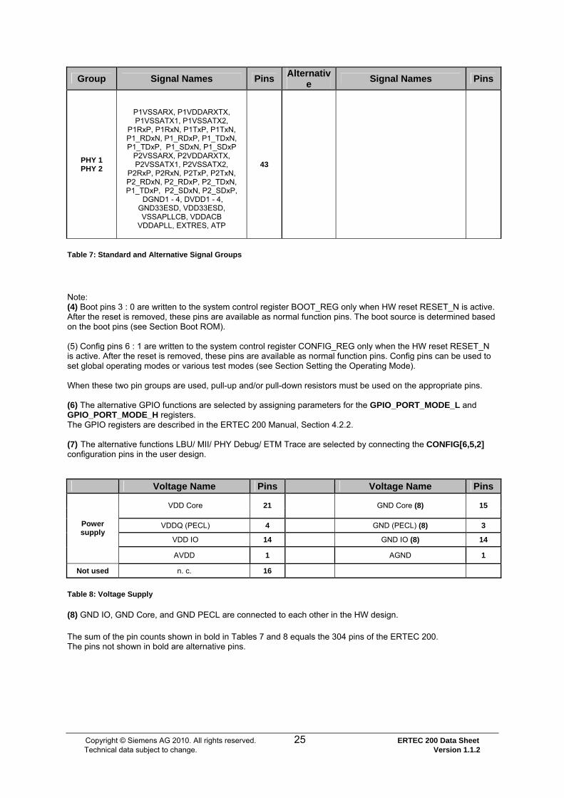
Standard and Alternative Signal Groups
The table below lists the standard and alternative signal groups with their signal names and pin count.
Group Signal Names Pins Alternative Signal Names Pins
PHY-LED
P1-/P2-DUPLEX_N P1-/P2-SPEED-100LED_N
P1-/P2-LINK-LED_N P1-/P2-RX-LED_N P1-/P2-TX-LED_N
P1-/P2-ACTIVE-LED_N
8
UART TXD , RXD , DCD_N , DSR_N , CTS_N 5
SPI SSPCTLOE, SSPOE, SCLKOUT, SSPRXD, SSPTXD, SFRMOUT,
SFRMIN, SCLKIN 8
GPIO
GPIO 31 : 0
GPIO[0], GPIO[1], GPIO[30] and GPIO[31] are
interrupt-capable
(6)
32
Other WDOUT_N, DBGACK, DBGREQ 3
JTAG/ DEBUG
TRST_N, TCK, TDI, TMS, TDO, SRST_N, TAP_SEL 7
CLOCK / RESET
TRACECLK, XENES, CLK_A, CLK_B, F_CLOCK, REF_CLK,
RESET_N 7
TEST TEST_N, TACT_N TMC1, TMC2 4
EMIF
A 23 : 0, D 31 :0, RD_N, WR_N, DTXR, OE_DRIVE_N,
RDY_PER_N, BE0_DQM0_N, BE1_DQM1_N, BE3_DQM2_N, BE3_DQM3_N, CLK_SDRAM, CS_SDRAM_N,
RAS_SDRAM_N, CAS_SDRAM_N,
CS_PER0_N- CS_PER0_N, WE_SDRAMCS_PER0_N
74 BOOT/
CONFIG BOOT 3 : 0 (4) CONFIG 6 : 1 (5)
10
PHY-DEBUG
RXD_P10, RXD_P11, RXD_P12, RXD_P13, RXD_P20, RXD_P21, RXD_P22, RXD_P23, COL_P1,
COL_P2, CRS_P1, CRS_P2, RX_ER_P1, RX_DV_P1,
RX_ER_P2, RX_DV_P2, RX_CLK_P1,
RX_CLK_P2, TXD_P10, TXD_P11, TXD_P12, TXD_P13, TXD_P20, TXD_P21,
TXD_P22, TXD_P23, TX_EN_P1, TX_ERR_P1, TX_EN_P2,
TX_ERR_P2, TX_CLK_P1, TX_CLK_P2,
SMI_MDC, SMI_MDIO, XRES_PHY
35
ETM ETMEXTOUT, ETMEXTIN1,
TRACEPKT 7 : 0 TRACESYNC PIPESTA 2 : 0
14
LBU
LBU_DB 15 : 0, LBU_A 20 : 0, LBU_BE0_N, LBU_BE1_N,
LBU_RDY_N, LBU_WR_N, LBU_RD_N, LBU_SEG0, LBU_SEG1,
LBU_CS_R_N, LBU_CS_M_N, LBU_IRQ0_N, LBU_IRQ1_N
(7)
48
GPIO GPIO 44 : 32 13
Copyright © Siemens AG 2010. All rights reserved. 25 ERTEC 200 Data Sheet Technical data subject to change. Version 1.1.2
Group Signal Names Pins Alternative Signal Names Pins
PHY 1 PHY 2
P1VSSARX, P1VDDARXTX, P1VSSATX1, P1VSSATX2,
P1RxP, P1RxN, P1TxP, P1TxN, P1_RDxN, P1_RDxP, P1_TDxN, P1_TDxP, P1_SDxN, P1_SDxP
P2VSSARX, P2VDDARXTX, P2VSSATX1, P2VSSATX2,
P2RxP, P2RxN, P2TxP, P2TxN, P2_RDxN, P2_RDxP, P2_TDxN, P1_TDxP, P2_SDxN, P2_SDxP,
DGND1 - 4, DVDD1 - 4, GND33ESD, VDD33ESD, VSSAPLLCB, VDDACB
VDDAPLL, EXTRES, ATP
43
Table 7: Standard and Alternative Signal Groups
Note: (4) Boot pins 3 : 0 are written to the system control register BOOT_REG only when HW reset RESET_N is active. After the reset is removed, these pins are available as normal function pins. The boot source is determined based on the boot pins (see Section Boot ROM). (5) Config pins 6 : 1 are written to the system control register CONFIG_REG only when the HW reset RESET_N is active. After the reset is removed, these pins are available as normal function pins. Config pins can be used to set global operating modes or various test modes (see Section Setting the Operating Mode). When these two pin groups are used, pull-up and/or pull-down resistors must be used on the appropriate pins. (6) The alternative GPIO functions are selected by assigning parameters for the GPIO_PORT_MODE_L and GPIO_PORT_MODE_H registers. The GPIO registers are described in the ERTEC 200 Manual, Section 4.2.2. (7) The alternative functions LBU/ MII/ PHY Debug/ ETM Trace are selected by connecting the CONFIG[6,5,2] configuration pins in the user design.
Voltage Name Pins Voltage Name Pins
VDD Core 21 GND Core (8) 15
VDDQ (PECL) 4 GND (PECL) (8) 3
VDD IO 14 GND IO (8) 14
Power supply
AVDD 1 AGND 1
Not used n. c. 16
Table 8: Voltage Supply
(8) GND IO, GND Core, and GND PECL are connected to each other in the HW design. The sum of the pin counts shown in bold in Tables 7 and 8 equals the 304 pins of the ERTEC 200. The pins not shown in bold are alternative pins.

Copyright © Siemens AG 2010. All rights reserved. 26 ERTEC 200 Data Sheet Technical data subject to change. Version 1.1.2
Operating/Limit Values and Characteristic Data
Maximum Limit Values
The following table indicates the “maximum limit values“ of the ERTEC 200. Operation outside these limit values can result in permanent damage to the block and is not permitted.
Characteristic Symbol Value Unit
Supply Voltage CORE 1.5 V VDD CORE -0.5 to +2.0 V Supply Voltage IO 3.3 V VDD IO -0.5 to +4.6 V
Supply Voltage PLL AVDD -0.5 to +2.0 V
Input Voltage (1.5 V CMOS) VIN -0.6 to VDDCore + 0.45 V Input Voltage (3.3 V LVTTL) VIN -0.6 to VDDIO + 0.6 V Input Voltage (5.0 V LVTTL) VIN -0.6 to VDDIO + 2.4 V
Storage Temperature TSTG -65 to +150 °C Junction Temperature TJ -40 to +120 °C
Table 9: Characteristic Data for Operating Values and Limit Values
Package – Thermal Specification
The ERTEC 200 is designed for operating temperatures between -40°C and +85°C. The following thermal resistance values are applicable to the package in a normal environment.
Air Flow Parameter (m/s) Symbol
0 0.2 1 2 Unit
Θja 30 27 23 21 K/W
Ψjt 0.2 0.3 0.6 0.8 K/W
Ψta 29.8 26.7 22.4 20.2 K/W
ΘjC 5.2 5.2 5.2 5.2 K/W
Table 10: Characteristic Data for Package – Thermal Resistance
Θja: Thermal resistance junction-to-ambient
Ψjt: Characteristic thermal parameter junction-to-top center of the package surface
Ψta: Characteristic thermal parameter top center of the package surface-to-ambient
The parameters are valid if no heat sink is used and at least 4-layer multilayer boards with solid ground and power supply layers are used. Maximum housing temperature: Tc = 105 °C ΘjC: Thermal resistance junction-to-case when a heat sink is used

Copyright © Siemens AG 2010. All rights reserved. 27 ERTEC 200 Data Sheet Technical data subject to change. Version 1.1.2
DC Operating Values
Parameter Symbol Min. Typ. Max. Unit Notes 1.5 V VDD Core 1.35 1.5 1.65 V 3.3 V VDD IO 3.0 3.3 3.6 V Supply Voltage PLL AVDD
AVDD_PCI 1.35 1.5 1.65 V
Ambient Temperature TA -40 +85 °C Output Voltage
High 3.3 V VOH 2.4 V Output Voltage
Low 3.3 V VOL 0.4 V 3.3 V
LVTTL 2.0 VDD IO Input Voltage High 5 V
comp. IO IOH
2.0 5.5 V
Input Voltage Low IOL 0 0.8 V
Positive Trigger Voltage Vp 1.2 2.4 V
Negative Trigger Voltage VN 0.6 1.8 V
Hysteresis Voltage
Schmitt Input
VH 0.3 1.5 V Input Rise Time tRI 0 200 ns Input Fall Time
Normal Input tFI 0 200 ns
Input Rise Time tRI 0 10 ms Input Fall Time
Schmitt Input tFI 0 10 ms 1.5 V IDD Core 400 535 mA Supply Current
100BASE-TX 3.3 V IDD IO 100 175 mA 1.5 V PDD Core 600 800 mW (9) 3.3 V PDD IO 330 570 mW (9)
Power Consumption 100BASE-TX total PDD 930 1370 mW (9)
1.5 V IDD Core 435 mA Supply Current 100BASE-FX 3.3 V IDD IO 85 mA
1.5 V PDD Core 650 mW (9) 3.3 V PDD IO 280 mW (9)
Power Consumption 100BASE-FX total PDD 930 mW (9)
Table 11: Characteristic Data of DC Operating Values

Copyright © Siemens AG 2010. All rights reserved. 28 ERTEC 200 Data Sheet Technical data subject to change. Version 1.1.2
(9) The ERTEC 200 has the following power loss when switched off in power-down mode: • PDD IO = 270 mW • PDD Core = 540 mW
The maximum current and power values cannot be guaranteed as absolute maximum values. These value are dependent on many different factors such as operating frequency, differing use of internal function groups, use of external interfaces, package temperature, and power supply. Different applications can have very different results. In general, the typical values were calculated on an evaluation board EB 200 with following conditions:
• VDD Core = 1.5 V, VDD IO = 3.3 V, TC = +25 °C • ARM946 CPU-Clock 150 MHz • SDRAM memorytest active • PHY settings to 100 Mbit Tx • all Ethernet Ports switching • LBU Interface not active
Maximum values were calculated for the following operating conditions:
VDD Core = 1.65 V, VDD IO = 3.6 V, TC = +85 °C.
Characteristic Data of Output Drivers
Signal Name Capacitive Load Unit Fan Out Notes Min. Max.
GPIO GPIO[0:7] 25 10 pF 9 mA 11
GPIO[8:26,30,31] 41 10 pF 6 mA 11
GPIO[27:29] 25 10 pF 24 mA 11
GPIO[32:40] 10 10 pF 6 mA 10
GPIO[41] 50 10 pF 9 mA 10
GPIO[42:44] 30 10 pF 6 mA 10
Clock/Debug/JTAC/ETM CLKP_B 25 10 pF 6 mA Clock
REF_CLK 25 10 pF 6 mA Clock SRST_N 10 10 pF 6 mA Debug reset
TRACECLK 10 10 pF 18 mA Clock PIPESTA [0:2]
TRACEPKT[0:7] ETMEXTOUT TRACESYNC
10 10 pF 6 mA ETM 10
TD0 30 10 pF 6 mA JTAG EMIF
DTXR XOE_DRIVE XCS_SDRAM
XRAS_SDRAM XCAS_SDRAM XWE_SDRAM
30 10 pF 9 mA
XCS_PER[0:3] 30 10 pF 6 mA

Copyright © Siemens AG 2010. All rights reserved. 29 ERTEC 200 Data Sheet Technical data subject to change. Version 1.1.2
A[0:23], D[0:31] XWR, XRD
XBE_DQM[0:3] 50 10 pF 9 mA
CLK_SDRAM 30 0 pF 9 mA
LBU
LBU_D[0:15] 50 10 pF 9 mA
LBU_RDY_N, LBU_IRQ0_N LBU_IRQ1_N 30 10 pF 6 mA
LBU_A[0:15], LBU_WR_N, LBU_RD_N, LBU_BE0_N, LBU_BE1_N
10 10 pF 6 mA
LBU_A[16:20], LBU_CS_R_N, LBU_CS_M_N,
LBU_SEG_0, LBU_SEG_1 25 10 pF 6 mA
Ethernet MII Port 1/2
TXD_P10, TXD_P11 TXD_P12, TXD_P13 TXD_P20, TXD_P21 TXD_P22, TXD_P23
TX_EN_P1, TX_EN_P2 TX_ER_P1, TX_ER_P2 SMI_MDIO, XRES_PHY
50 10 pF 9 mA 10
RX_CLK_P1, RX_CLK_P2 30 10 pF 6 mA 10
PHY 1/2
P1TDXP, P1TDXN P2TDXP, P2TDXN 25 10 pF 12 mA
Table 12: Characteristic Data of Output Drivers
(10) These outputs are alternative LBU interface pins and have the same values as the corresponding LBU signal. (11) Alternative outputs of GPIO[0:31] have the same values.

Copyright © Siemens AG 2010. All rights reserved. 30 ERTEC 200 Data Sheet Technical data subject to change. Version 1.1.2
Input Clock Specification
Parameter Symbol Minimum Maximum Unit Notes
CPU Clock Processor clock frequency PFC 50/100/150 MHz
Processor clock period PTC 20/10/6,66 ns
Oscillator clock Oscillator clock frequency OSC_FC 25 25 MHz +/- 50 ppm
Oscillator clock period OSC_TC 40 ns REF clock frequency REF_Clk_FC 25 25 MHz +/- 50 ppm
REF clock period REF_Clk_TC 40 ns REF clock stability REF_Clk_TCS +/- 0.2 ns
JTAG/TRACE clock JTAGClk frequency JTAG_FC 10 MHz
JTAGClk period JTAG_TC 100 ns
PHY clock MII mode PHY_TxClk MII frequency PHY_Tx_M_FC 2.5 25 MHz
PHY_TxClk MII period PHY_Tx_M_TC 40 400 ns PHY_TxClk MII input High
time PHY_Tx_M_TCH 35% of nominal period
65% of nominal period ns
PHY_TxClk MII input Low time PHY_Tx_M_TCL 35% of nominal
period 65% of nominal
period ns
PHY_RxClk MII frequency PHY_Rx_M_FC 2.5 25 MHz
PHY_RxClk MII period PHY_Rx_M_TC 40 400 ns PHY_RxClk MII input High
time PHY_Rx_M_TCH 35% of nominal period
65% of nominal period ns
PHY_RxClk MII input Low time PHY_Rx_M_TCL 35% of nominal
period 65% of nominal
period ns
SDRAM clock SDRAM_SysClk frequency SDRAM_FC 50 MHz
SDRAM_SysClk period SDRAM_TC 20 ns SDRAM_SysClk stability SDRAM_TCS +/- 0.2 ns
SDRAM_SysClk input High time SDRAM_TCH 40% of nominal
period 60% of nominal
period ns
SDRAM_SysClk input Low time SDRAM_TCL 40% of nominal
period 60% of nominal
period ns
SPI clock SCLKIN SPI slave mode
frequency SPI_S_FC 0 4.16 MHz
SCLKIN SPI slave mode low time SPI_S_TCL 120 ns
SCLKIN SPI slave mode high time SPI_S_TCH 120 ns
SCLKOUT SPI master mode frequency SPI_M_FC 769x10-6 25 MHz
SCLKOUT SPI master mode period SPI_M_TC 40 1.3x10⁶ ns
SCLKOUT SPI master mode low time SPI_M_TCL 45% of nominal
period 55% of nominal
period ns
SCLKOUT SPI master mode high time SPI_M_TCH 45% of nominal
period 55% of nominal
period ns
Table 13: Characteristic Data of Input/Clock

Copyright © Siemens AG 2010. All rights reserved. 31 ERTEC 200 Data Sheet Technical data subject to change. Version 1.1.2

Copyright © Siemens AG 2010. All rights reserved. 32 ERTEC 200 Data Sheet Technical data subject to change. Version 1.1.2
I/O Specification
1. Features of trace interface for “full rate“ and “half rate“ modes: In “half rate“ mode, Tc is the interval between two falling edges. In “full rate“ mode, Tc is the interval between a rising edge and a falling edge.
2. Other GPIO signals: DBGACK, WD_WDOUT_N, IRT_TRIG_TRACE_UNIT 3. Other ETM trace signals: ETMEXTOUT, ETMEXTIN1 4. Reference is falling edge of TCK 5. Access by the host is asynchronous to the AHB clock of the ERTEC 200. For this reason, it is
synchronized with the AHB clock.
Input (ns) Output (ns) Output Current (mA)
Signal Setup Time
TIS min
Hold Time
TIH min
Hold Time
TOH min
Valid Delay TOV min
I/O H min
I/O L min
Clock Alternative Notes
GPIO GPIO[7:0] 9 9 async PHY-LED GPIO[26:8] 6 6 async SPI,UART 2 GPIO[29:27] 24 24 async GPIO[31:30] 6 6 async DBGREQ
GPIO (LBU Alternative Function 2 – 4) GPIO[44:32] 6 6 async
EMIF D[31 :0] 10 0 2 12.5 9 9 ClkSDRAM A[23 :0] na na 2 11 9 9 ClkSDRAM
BE_DQM_N[3 :0] na na 2 11 9 9 ClkSDRAM CAS_SDRAM_N na na 2 11 9 9 ClkSDRAM RAS_SDRAM_N na na 2 11 9 9 ClkSDRAM WE_SDRAM_N na na 2 11 9 9 ClkSDRAM CS_SDRAM_N na na 2 11 9 9 ClkSDRAM RDY_PER_N na na na na 9 9 async
WR_N na na 2 11 9 9 ClkSDRAM RD_N na na 2 11 9 9 ClkSDRAM
DTR_N na na dc dc 9 9 async OE_DRIVER_N na na na na 9 9 async CS_PER_N[3:0] na na na na 6 6 async
LBU LBU_D[15 :0] 10.4 0.5 1 9.2 9 9 async 5 LBU_A[20 :0] 10.4 0.5 1 9.2 6 6 async 3,5 LBU_RDY_N 10.4 0.5 1 9.2 6 6 async 5 LBU_IRQ0_N, LBU_IRQ1_N 10.4 0.5 1 9.2 6 6 async 5
LBU_SEG[1:0] 10.4 0.5 1 9.2 6 6 async 5 LBU_CS_M_N, LBU_CS_R_N 10.4 0.5 1 9.2 6 6 async 5
LBU_WR_N, LBU_RD_N 10.4 0.5 1 9.2 6 6 async 5
LBU_BE0_N, LBU_BE1_N 10.4 0.5 1 9.2 6 6 async 5
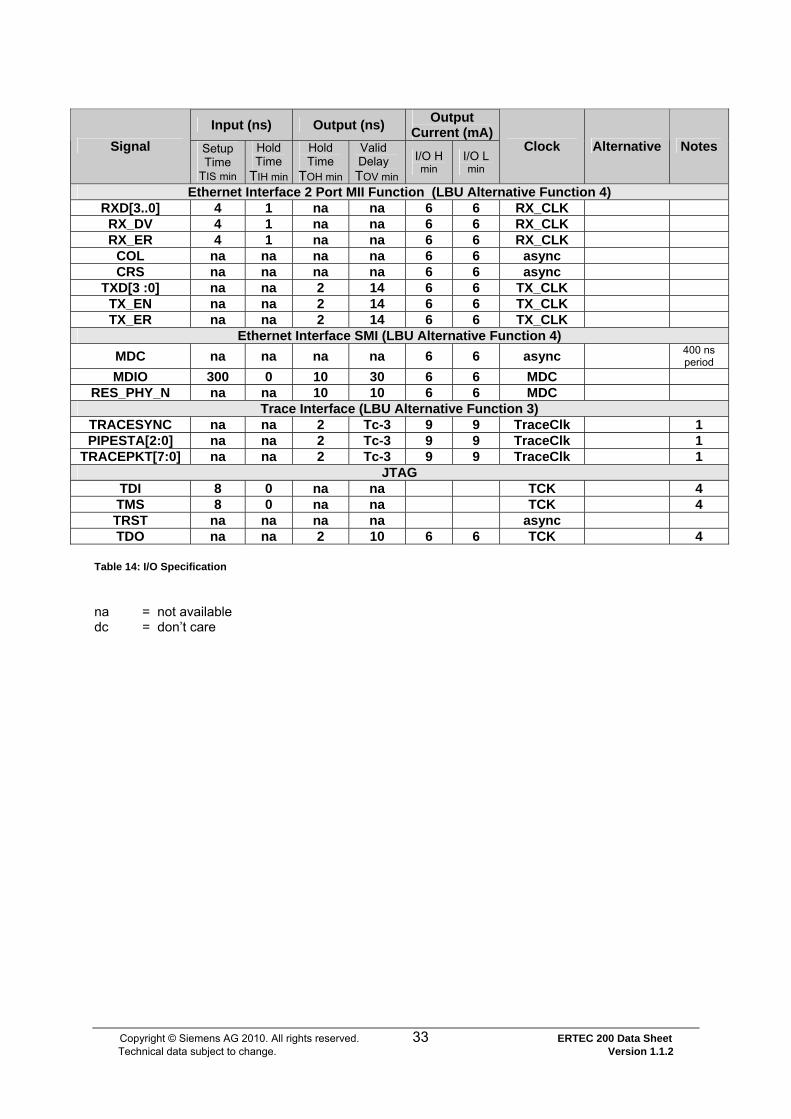
Copyright © Siemens AG 2010. All rights reserved. 33 ERTEC 200 Data Sheet Technical data subject to change. Version 1.1.2
Input (ns) Output (ns) Output Current (mA)
Signal Setup Time
TIS min
Hold Time
TIH min
Hold Time
TOH min
Valid Delay TOV min
I/O H min
I/O L min
Clock Alternative Notes
Ethernet Interface 2 Port MII Function (LBU Alternative Function 4) RXD[3..0] 4 1 na na 6 6 RX_CLK
RX_DV 4 1 na na 6 6 RX_CLK RX_ER 4 1 na na 6 6 RX_CLK
COL na na na na 6 6 async CRS na na na na 6 6 async
TXD[3 :0] na na 2 14 6 6 TX_CLK TX_EN na na 2 14 6 6 TX_CLK TX_ER na na 2 14 6 6 TX_CLK
Ethernet Interface SMI (LBU Alternative Function 4) MDC na na na na 6 6 async 400 ns
period MDIO 300 0 10 30 6 6 MDC
RES_PHY_N na na 10 10 6 6 MDC Trace Interface (LBU Alternative Function 3)
TRACESYNC na na 2 Tc-3 9 9 TraceClk 1 PIPESTA[2:0] na na 2 Tc-3 9 9 TraceClk 1
TRACEPKT[7:0] na na 2 Tc-3 9 9 TraceClk 1 JTAG
TDI 8 0 na na TCK 4 TMS 8 0 na na TCK 4 TRST na na na na async TDO na na 2 10 6 6 TCK 4
Table 14: I/O Specification
na = not available dc = don’t care

Copyright © Siemens AG 2010. All rights reserved. 34 ERTEC 200 Data Sheet Technical data subject to change. Version 1.1.2

Copyright © Siemens AG 2010. All rights reserved. 35 ERTEC 200 Data Sheet Technical data subject to change. Version 1.1.2
LBU-Timing
LBU Read from ERTEC 200 with separate Read/Write line (LBU_RDY_N active low)
LBU_CS_R_N/ LBU_CS_M_N
LBU_RD_N
LBU_A(20:0)A/ LBU_SEG(1:0)/ LBU_BE(1:0)_N
LBU_RDY_N
LBU_D(15:0)
t CSRS
tARS
t RRE
t RDE tRTDt RDH
t RAH
t RCSH
tRAP
t RR
Figure 3: LBU-Read-Sequence with separate RD/WR line
Parameter Description Min Max
tCSRS chip select asserted to read pulse asserted delay 0 ns
tARS address valid to read pulse asserted setup time 0 ns
tRRE read pulse asserted to ready enabled delay 5 ns 12 ns
tRDE read pulse asserted to data enable delay 5 ns 12 ns
tRAP ready active pulse width 17 ns 23 ns
tRTD ready asserted to data valid delay 5 ns
tRCSH read pulse deasserted to chip select deasserted delay 0 ns
tRAH address valid to read pulse deasserted hold time 0 ns
tRDH data valid/enabled to read pulse deasserted hold time 0 ns 12 ns
tRR read recovery time 25 ns
Table 15: LBU read access timing with seperate Read/Write line

Copyright © Siemens AG 2010. All rights reserved. 36 ERTEC 200 Data Sheet Technical data subject to change. Version 1.1.2
LBU Write to ERTEC 200 with separate Read/Write line (LBU_RDY_N active low)
LBU_CS_R_N/ LBU_CD_M_N
LBU_WR_N
LBU_A(20:0)/ LBU_SEG(1:0) LBU_BE(1:0)_N
LBU_RDY_N
LBU_D(15:0)
t CSWS
tAWS
t WRE
t WDV t WDH
t WAH
t WCSH
tRTW
tRAP
t WR
Figure 4: LBU-Write-Sequence with separate RD/WR line Parameter Description Min Max
tCSWS chip select asserted to write pulse asserted delay 0 ns tAWS address valid to write pulse asserted setup time 0 ns tWRE write pulse asserted to ready enabled delay 5 ns 12 ns tWDV write pulse asserted to data valid delay 40 ns tRAP ready active pulse width 17 ns 23 ns
tWCSH write pulse deasserted to chip select deasserted delay 0 ns tWAH address valid to write pulse deasserted hold time 0 ns tRTW ready asserted to write pulse deasserted delay 0 ns tWDH data valid/enabled to read pulse deasserted hold time 0 ns tWR write recovery time 25 ns
Table 16: LBU write access timing with seperate Read/Write line

Copyright © Siemens AG 2010. All rights reserved. 37 ERTEC 200 Data Sheet Technical data subject to change. Version 1.1.2
LBU Read from ERTEC 200 with common Read/Write line (LBU_RDY_N active low)
LBU_CS_R_N/ LBU_CS_M_N
LBU_WR_N
LBU_A(20:0)/ LBU_SEG(1:0)/ LBU_BE(1:0)_N
LBU_RDY_N
LBU_D(15:0)
t WCS
tACS
t CRE
t CDE tRTDt CDH
tCAH
t CWH
tRAP
t RR
Figure 5: LBU-Read-Sequence with common RD/WR line Parameter Description Min Max
tWCS write signal deasserted to chip select asserted setup time 2 ns tACS address valid to chip select asserted setup time 0 ns tCRE chip select asserted to ready enabled delay 5 ns 12 ns tCDE chip select asserted to data enable delay 5 ns 12 ns tRAP ready active pulse width 17 ns 23 ns tRTD ready asserted to data valid delay 5 ns tCWH write signal inactive to chip select deasserted hold time 0 ns tRAH address valid to chip select deasserted hold time 0 ns tRDH data valid/enabled to chip select deasserted hold time 0 ns 12 ns tRR read recovery time 25 ns
Table 17: LBU read access timing with common Read/Write line
Copyright © Siemens AG 2010. All rights reserved. 38 ERTEC 200 Data Sheet Technical data subject to change. Version 1.1.2
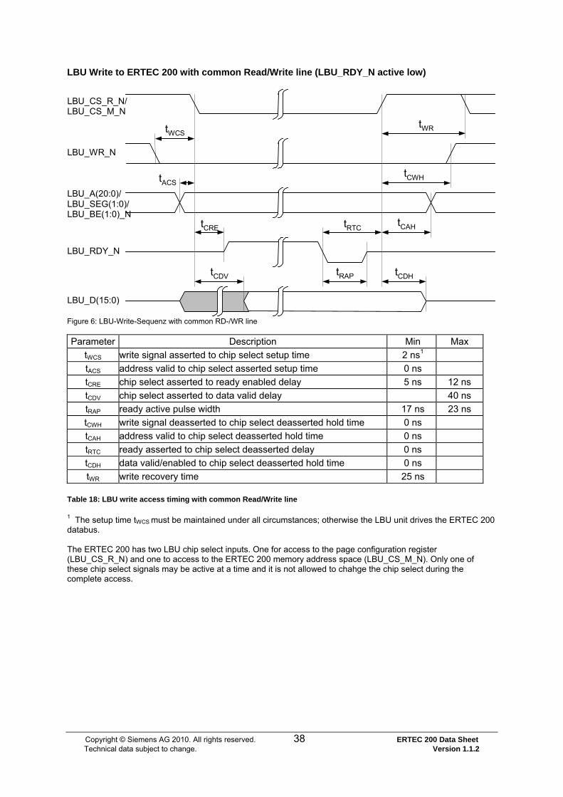
LBU Write to ERTEC 200 with common Read/Write line (LBU_RDY_N active low)
LBU_CS_R_N/ LBU_CS_M_N
LBU_WR_N
LBU_A(20:0)/ LBU_SEG(1:0)/ LBU_BE(1:0)_N
LBU_RDY_N
LBU_D(15:0)
tWCS
tACS
t CRE
t CDV tCDH
t CAH
t CWH
tRTC
tRAP
t WR
Figure 6: LBU-Write-Sequenz with common RD-/WR line Parameter Description Min Max
tWCS write signal asserted to chip select setup time 2 ns1 tACS address valid to chip select asserted setup time 0 ns tCRE chip select asserted to ready enabled delay 5 ns 12 ns tCDV chip select asserted to data valid delay 40 ns tRAP ready active pulse width 17 ns 23 ns tCWH write signal deasserted to chip select deasserted hold time 0 ns tCAH address valid to chip select deasserted hold time 0 ns tRTC ready asserted to chip select deasserted delay 0 ns tCDH data valid/enabled to chip select deasserted hold time 0 ns tWR write recovery time 25 ns
Table 18: LBU write access timing with common Read/Write line
1 The setup time tWCS must be maintained under all circumstances; otherwise the LBU unit drives the ERTEC 200 databus. The ERTEC 200 has two LBU chip select inputs. One for access to the page configuration register (LBU_CS_R_N) and one to access to the ERTEC 200 memory address space (LBU_CS_M_N). Only one of these chip select signals may be active at a time and it is not allowed to chahge the chip select during the complete access.

Copyright © Siemens AG 2010. All rights reserved. 39 ERTEC 200 Data Sheet Technical data subject to change. Version 1.1.2
.
SPI timing specifications
Remarks: 1. Note different serial clock frequency ranges for SPI slave and master
modes as given in Table 13. 2. Timing diagrams are shown for TI-format. Other transfer formats can be
configured, however the AC-timings (setup/hold times, delays) remain unchanged.
3. Not every external SPI device, that is connected to ERTEC 200, requires usage of all available SPI signals.
SPI interface configured to slave mode
Parameter Symbol Condition MIN. MAX. Unit
SPI1_SSPRXD setup time tSSPRXDS - 20 - ns
SPI1_SSPRXD hold time tSSPRXDH - 60 - ns
SPI1_SFRMIN setup time tSFRMINS - 40 - ns
SPI1_SFRMIN hold time tSSPRMINH - 20 - ns
SPI1_SSPTXD delay tSSPTXDD - - 40 ns
SPI1_SSPOE delay tSSPOED - - 40 ns
Table 19: SPI Timing Specifications (slave mode)
Figure 7: SPI Timing in Slave Mode (TI-format Example)
Copyright © Siemens AG 2010. All rights reserved. 40 ERTEC 200 Data Sheet Technical data subject to change. Version 1.1.2
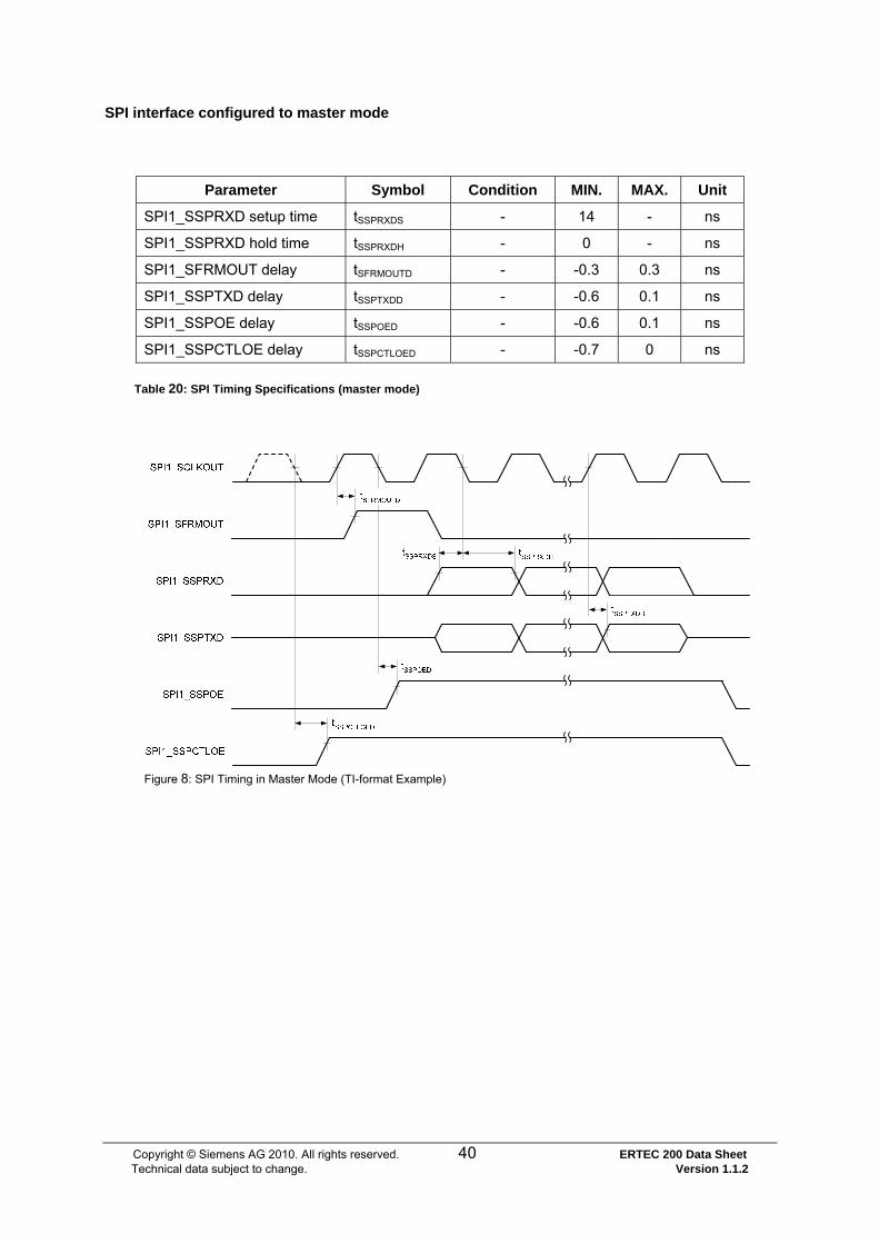
SPI interface configured to master mode
Parameter Symbol Condition MIN. MAX. Unit
SPI1_SSPRXD setup time tSSPRXDS - 14 - ns
SPI1_SSPRXD hold time tSSPRXDH - 0 - ns
SPI1_SFRMOUT delay tSFRMOUTD - -0.3 0.3 ns
SPI1_SSPTXD delay tSSPTXDD - -0.6 0.1 ns
SPI1_SSPOE delay tSSPOED - -0.6 0.1 ns
SPI1_SSPCTLOE delay tSSPCTLOED - -0.7 0 ns
Table 20: SPI Timing Specifications (master mode)
Figure 8: SPI Timing in Master Mode (TI-format Example)
Copyright © Siemens AG 2010. All rights reserved. 41 ERTEC 200 Data Sheet Technical data subject to change. Version 1.1.2
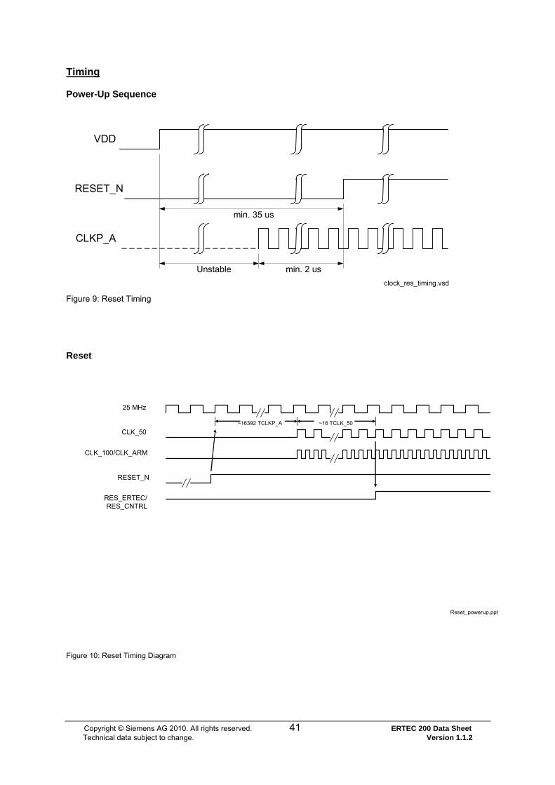
Timing
Power-Up Sequence
VDD
RESET_N
CLKP_A
min. 35 us
Unstable min. 2 usclock_res_timing.vsd
Figure 9: Reset Timing
Reset
25 MHz
RESET_N
CLK_50
RES_ERTEC/RES_CNTRL
CLK_100/CLK_ARM
~16392 TCLKP_A ~16 TCLK_50
Reset_powerup.ppt
Figure 10: Reset Timing Diagram
Recommended