Embed Size (px)
Citation preview
The information in this document is subject to change without notice. Before using this document, pleaseconfirm that this is the latest version.Not all products and/or types are available in every country. Please check with an NEC Electronics sales representative for availability and additional information.
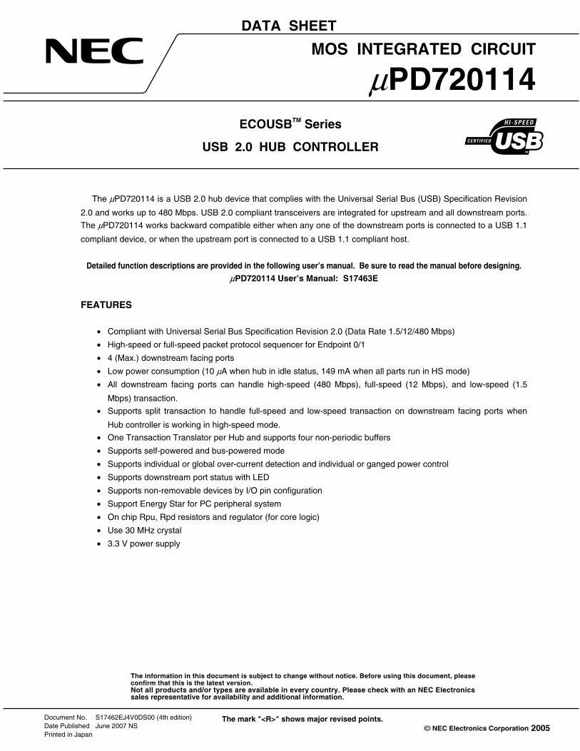
MOS INTEGRATED CIRCUIT
μPD720114ECOUSBTM Series
USB 2.0 HUB CONTROLLER
Document No. S17462EJ4V0DS00 (4th edition) Date Published June 2007 NS Printed in Japan
DATA SHEET
The mark "<R>" shows major revised points. 2005
The μPD720114 is a USB 2.0 hub device that complies with the Universal Serial Bus (USB) Specification Revision
2.0 and works up to 480 Mbps. USB 2.0 compliant transceivers are integrated for upstream and all downstream ports.
The μPD720114 works backward compatible either when any one of the downstream ports is connected to a USB 1.1
compliant device, or when the upstream port is connected to a USB 1.1 compliant host.
Detailed function descriptions are provided in the following user’s manual. Be sure to read the manual before designing. μPD720114 User’s Manual: S17463E
FEATURES
• Compliant with Universal Serial Bus Specification Revision 2.0 (Data Rate 1.5/12/480 Mbps)
• High-speed or full-speed packet protocol sequencer for Endpoint 0/1
• 4 (Max.) downstream facing ports
• Low power consumption (10 μA when hub in idle status, 149 mA when all parts run in HS mode)
• All downstream facing ports can handle high-speed (480 Mbps), full-speed (12 Mbps), and low-speed (1.5
Mbps) transaction.
• Supports split transaction to handle full-speed and low-speed transaction on downstream facing ports when
Hub controller is working in high-speed mode.
• One Transaction Translator per Hub and supports four non-periodic buffers
• Supports self-powered and bus-powered mode
• Supports individual or global over-current detection and individual or ganged power control
• Supports downstream port status with LED
• Supports non-removable devices by I/O pin configuration
• Support Energy Star for PC peripheral system
• On chip Rpu, Rpd resistors and regulator (for core logic)
• Use 30 MHz crystal
• 3.3 V power supply
Data Sheet S17462EJ4V0DS 2
μPD720114
ORDERING INFORMATION
Part Number Package Remark
μPD720114GA-9EU-A 48-pin plastic TQFP (Fine pitch) (7 × 7) Lead-free product
μPD720114GA-YEU-A 48-pin plastic TQFP (Fine pitch) (7 × 7) Lead-free product
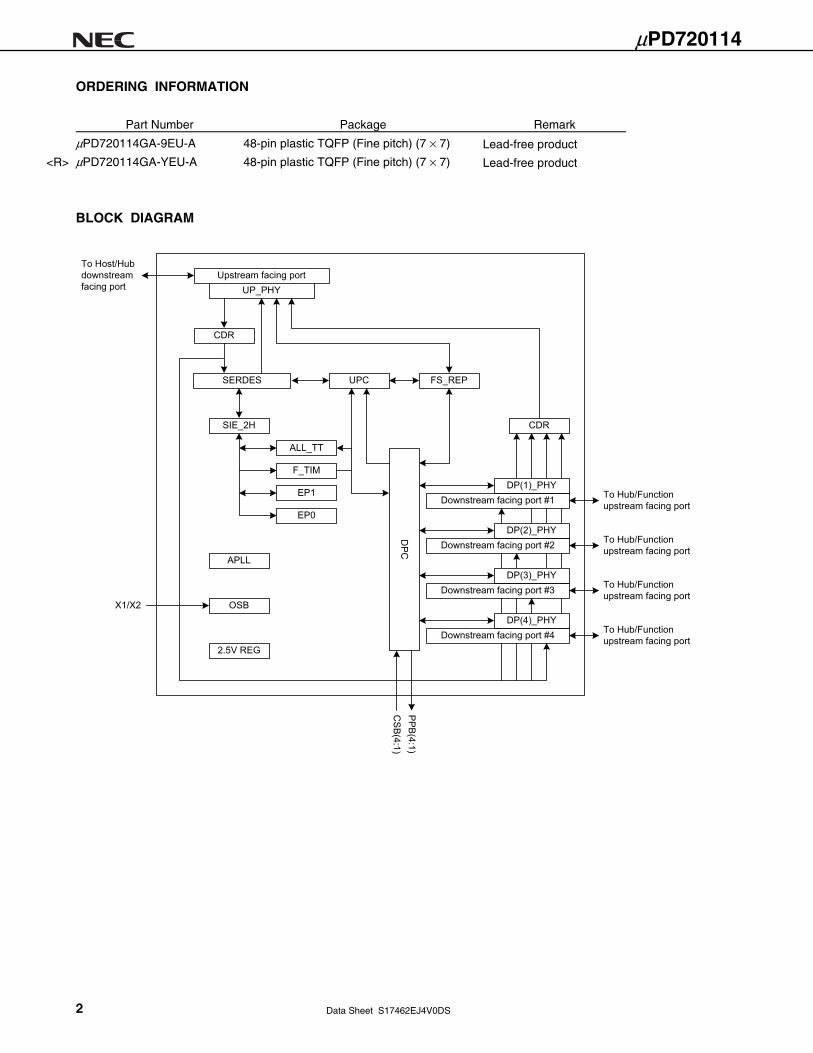
BLOCK DIAGRAM
Upstream facing portUP_PHY
Downstream facing port #1
SERDES
SIE_2H
CDR
APLL
OSB
UPC
ALL_TT
F_TIM
EP1
EP0
DP(1)_PHY
Downstream facing port #2DP(2)_PHY
Downstream facing port #3DP(3)_PHY
Downstream facing port #4DP(4)_PHY
DP
C
FS_REP
To Host/Hubdownstreamfacing port
X1/X2
PPB
(4:1)C
SB
(4:1)
To Hub/Function upstream facing port
To Hub/Function upstream facing port
To Hub/Function upstream facing port
To Hub/Function upstream facing port
CDR
2.5V REG
<R>
Data Sheet S17462EJ4V0DS 3
μPD720114
APLL : Generates all clocks of Hub.
ALL_TT : Translates the high-speed transactions (split transactions) for full/low-speed device
to full/low-speed transactions. ALL_TT buffers the data transfer from either
upstream or downstream direction. For OUT transaction, ALL_TT buffers data from
upstream port and sends it out to the downstream facing ports after speed
conversion from high-speed to full/low-speed. For IN transaction, ALL_TT buffers
data from downstream ports and sends it out to the upstream facing ports after
speed conversion from full/low-speed to high-speed.
CDR : Data & clock recovery circuit
DPC : Downstream Port Controller handles Port Reset, Enable, Disable, Suspend and
Resume
DP(n)_PHY : Downstream transceiver supports high-speed (480 Mbps), full-speed (12 Mbps), and
low-speed (1.5 Mbps) transaction
EP0 : Endpoint 0 controller
EP1 : Endpoint 1 controller
F_TIM (Frame Timer) : Manages hub’s synchronization by using micro-SOF which is received at upstream
port, and generates SOF packet when full/low-speed device is attached to
downstream facing port.
FS_REP : Full/low-speed repeater is enabled when the μPD720114 are worked at full-speed
mode
OSB : Oscillator Block
2.5V REG : On chip 2.5V regulator
SERDES : Serializer and Deserializer
SIE_2H : Serial Interface Engine (SIE) controls USB2.0 and 1.1 protocol sequencer.
UP_PHY : Upstream Transceiver supports high-speed (480 Mbps), full-speed (12 Mbps)
transaction
UPC : Upstream Port Controller handles Suspend and Resume
Data Sheet S17462EJ4V0DS 4
μPD720114
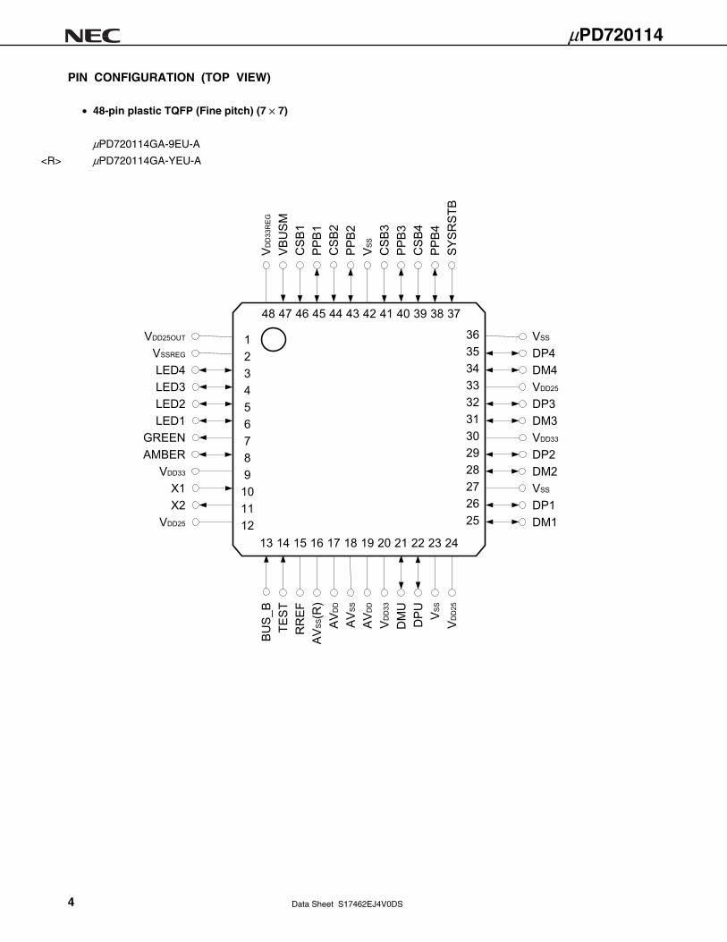
PIN CONFIGURATION (TOP VIEW)
• 48-pin plastic TQFP (Fine pitch) (7 × 7)
μPD720114GA-9EU-A
μPD720114GA-YEU-A
44
BUS_
BTE
STR
REF
AVSS
(R)
AVD
D
AVS
S
AVD
D
VD
D33
DM
UD
PU
VSS
VD
D25
VSS
DP4DM4VDD25
DP3DM3VDD33
DP2DM2VSS
DP1DM1
VDD25OUT
VSSREG
LED4LED3LED2LED1
GREENAMBER
VDD33
X1X2
VDD25
VDD
33R
EG
VBU
SM
CSB
1PP
B1C
SB2
PPB2
VSS
CSB
3PP
B3C
SB4
PPB4
SY
SR
STB
123456789101112
363534333231302928272625
13 1614 15 17 18 19 20 21 22 23 24
3738394041424345464748
<R>
Data Sheet S17462EJ4V0DS 5
μPD720114
Pin No. Pin Name Pin No. Pin Name Pin No. Pin Name Pin No. Pin Name
1 VDD25OUT 13 BUS_B 25 DM1 37 SYSRSTB
2 VSSREG 14 TEST 26 DP1 38 PPB4
3 LED4 15 RREF 27 VSS 39 CSB4
4 LED3 16 AVSS(R) 28 DM2 40 PPB3
5 LED2 17 AVDD 29 DP2 41 CSB3
6 LED1 18 AVSS 30 VDD33 42 VSS
7 GREEN 19 AVDD 31 DM3 43 PPB2
8 AMBER 20 VDD33 32 DP3 44 CSB2
9 VDD33 21 DMU 33 VDD25 45 PPB1
10 X1 22 DPU 34 DM4 46 CSB1
11 X2 23 VSS 35 DP4 47 VBUSM
12 VDD25 24 VDD25 36 VSS 48 VDD33REG
Remark AVSS(R) should be used to connect RREF through 1 % precision reference resistor of 2.43 kΩ.
Data Sheet S17462EJ4V0DS 6
μPD720114
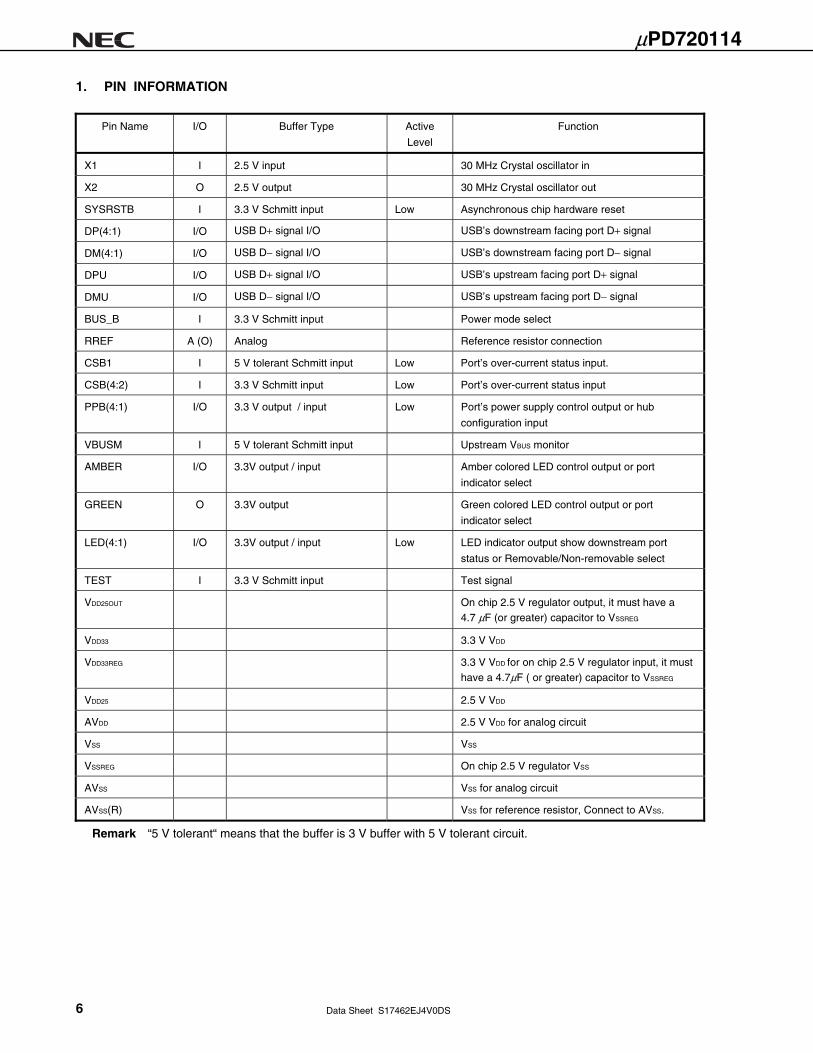
1. PIN INFORMATION
Pin Name I/O Buffer Type Active
Level
Function
X1 I 2.5 V input 30 MHz Crystal oscillator in
X2 O 2.5 V output 30 MHz Crystal oscillator out
SYSRSTB I 3.3 V Schmitt input Low Asynchronous chip hardware reset
DP(4:1) I/O USB D+ signal I/O USB’s downstream facing port D+ signal
DM(4:1) I/O USB D− signal I/O USB’s downstream facing port D− signal
DPU I/O USB D+ signal I/O USB’s upstream facing port D+ signal
DMU I/O USB D− signal I/O USB’s upstream facing port D− signal
BUS_B I 3.3 V Schmitt input Power mode select
RREF A (O) Analog Reference resistor connection
CSB1 I 5 V tolerant Schmitt input Low Port’s over-current status input.
CSB(4:2) I 3.3 V Schmitt input Low Port’s over-current status input
PPB(4:1) I/O 3.3 V output / input Low Port’s power supply control output or hub
configuration input
VBUSM I 5 V tolerant Schmitt input Upstream VBUS monitor
AMBER I/O 3.3V output / input Amber colored LED control output or port
indicator select
GREEN O 3.3V output Green colored LED control output or port
indicator select
LED(4:1) I/O 3.3V output / input Low LED indicator output show downstream port
status or Removable/Non-removable select
TEST I 3.3 V Schmitt input Test signal
VDD25OUT On chip 2.5 V regulator output, it must have a 4.7 μF (or greater) capacitor to VSSREG
VDD33 3.3 V VDD
VDD33REG 3.3 V VDD for on chip 2.5 V regulator input, it must have a 4.7μF ( or greater) capacitor to VSSREG
VDD25 2.5 V VDD
AVDD 2.5 V VDD for analog circuit
VSS VSS
VSSREG On chip 2.5 V regulator VSS
AVSS VSS for analog circuit
AVSS(R) VSS for reference resistor, Connect to AVSS.
Remark “5 V tolerant“ means that the buffer is 3 V buffer with 5 V tolerant circuit.
Data Sheet S17462EJ4V0DS 7
μPD720114
2. ELECTRICAL SPECIFICATIONS
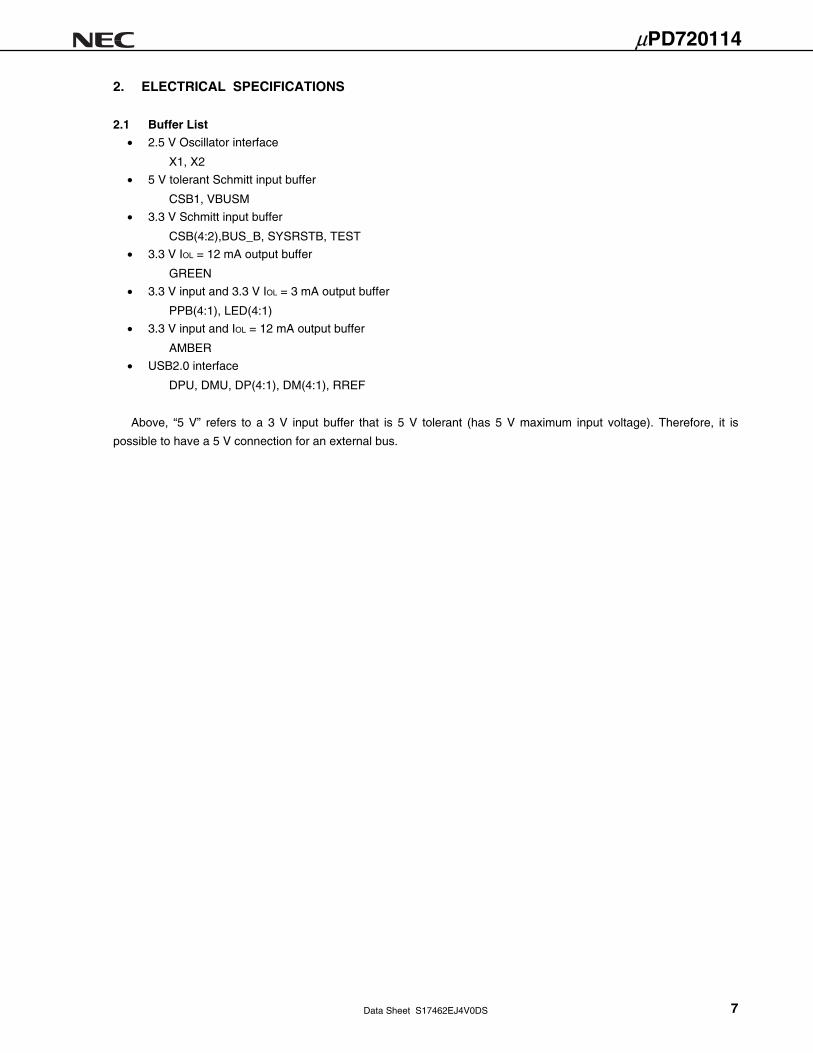
2.1 Buffer List • 2.5 V Oscillator interface
X1, X2
• 5 V tolerant Schmitt input buffer
CSB1, VBUSM
• 3.3 V Schmitt input buffer
CSB(4:2),BUS_B, SYSRSTB, TEST
• 3.3 V IOL = 12 mA output buffer
GREEN
• 3.3 V input and 3.3 V IOL = 3 mA output buffer
PPB(4:1), LED(4:1)
• 3.3 V input and IOL = 12 mA output buffer
AMBER
• USB2.0 interface
DPU, DMU, DP(4:1), DM(4:1), RREF
Above, “5 V” refers to a 3 V input buffer that is 5 V tolerant (has 5 V maximum input voltage). Therefore, it is
possible to have a 5 V connection for an external bus.
Data Sheet S17462EJ4V0DS 8
μPD720114
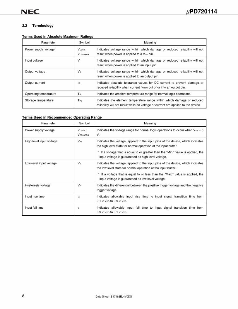
2.2 Terminology
Terms Used in Absolute Maximum Ratings
Parameter Symbol Meaning
Power supply voltage VDD33,
VDD33REG
Indicates voltage range within which damage or reduced reliability will not
result when power is applied to a VDD pin.
Input voltage VI Indicates voltage range within which damage or reduced reliability will not
result when power is applied to an input pin.
Output voltage VO Indicates voltage range within which damage or reduced reliability will not
result when power is applied to an output pin.
Output current IO Indicates absolute tolerance values for DC current to prevent damage or
reduced reliability when current flows out of or into an output pin.
Operating temperature TA Indicates the ambient temperature range for normal logic operations.
Storage temperature Tstg Indicates the element temperature range within which damage or reduced
reliability will not result while no voltage or current are applied to the device.
Terms Used in Recommended Operating Range
Parameter Symbol Meaning
Power supply voltage VDD33,
VDD33REG
Indicates the voltage range for normal logic operations to occur when VSS = 0
V.
High-level input voltage VIH Indicates the voltage, applied to the input pins of the device, which indicates
the high level state for normal operation of the input buffer.
* If a voltage that is equal to or greater than the “Min.” value is applied, the
input voltage is guaranteed as high level voltage.
Low-level input voltage VIL Indicates the voltage, applied to the input pins of the device, which indicates
the low level state for normal operation of the input buffer.
* If a voltage that is equal to or less than the “Max.” value is applied, the
input voltage is guaranteed as low level voltage.
Hysteresis voltage VH Indicates the differential between the positive trigger voltage and the negative
trigger voltage.
Input rise time tri Indicates allowable input rise time to input signal transition time from0.1 × VDD to 0.9 × VDD.
Input fall time tfi Indicates allowable input fall time to input signal transition time from0.9 × VDD to 0.1 × VDD.
Data Sheet S17462EJ4V0DS 9
μPD720114
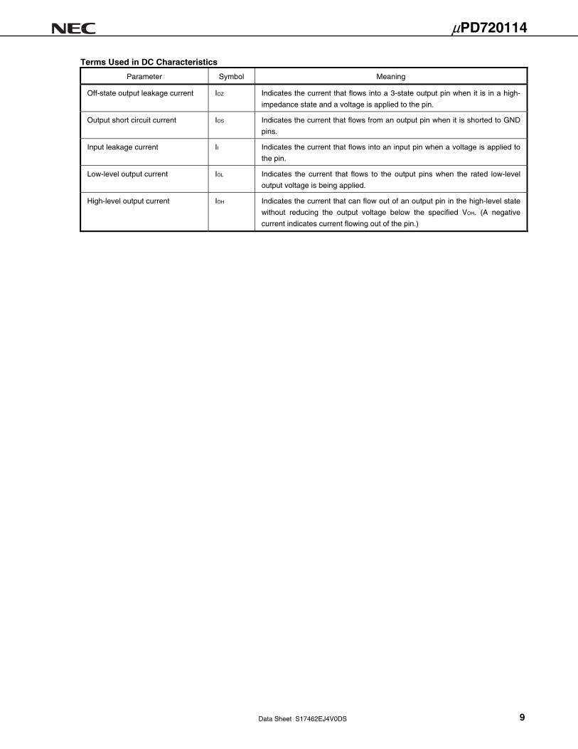
Terms Used in DC Characteristics
Parameter Symbol Meaning
Off-state output leakage current IOZ Indicates the current that flows into a 3-state output pin when it is in a high-
impedance state and a voltage is applied to the pin.
Output short circuit current IOS Indicates the current that flows from an output pin when it is shorted to GND
pins.
Input leakage current II Indicates the current that flows into an input pin when a voltage is applied to
the pin.
Low-level output current IOL Indicates the current that flows to the output pins when the rated low-level
output voltage is being applied.
High-level output current IOH Indicates the current that can flow out of an output pin in the high-level state
without reducing the output voltage below the specified VOH. (A negative
current indicates current flowing out of the pin.)
Data Sheet S17462EJ4V0DS 10
μPD720114
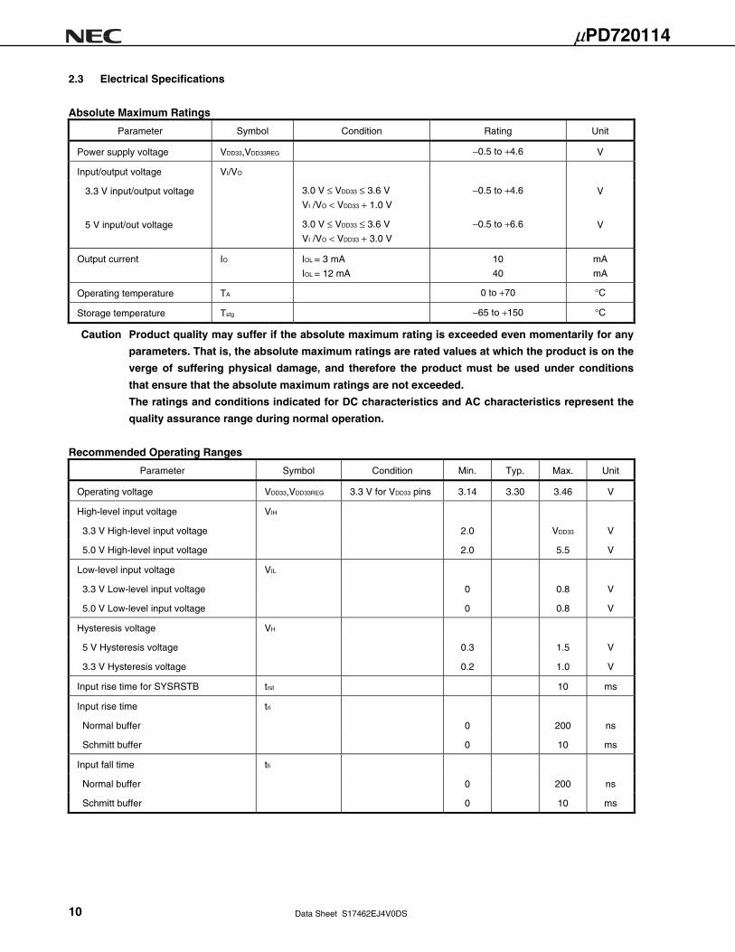
2.3 Electrical Specifications
Absolute Maximum Ratings
Parameter Symbol Condition Rating Unit
Power supply voltage VDD33,VDD33REG −0.5 to +4.6 V
Input/output voltage VI/VO
3.3 V input/output voltage 3.0 V ≤ VDD33 ≤ 3.6 V
VI /VO < VDD33 + 1.0 V
−0.5 to +4.6 V
5 V input/out voltage 3.0 V ≤ VDD33 ≤ 3.6 V
VI /VO < VDD33 + 3.0 V
−0.5 to +6.6 V
Output current IO IOL = 3 mA
IOL = 12 mA
10
40
mA
mA
Operating temperature TA 0 to +70 °C
Storage temperature Tstg −65 to +150 °C
Caution Product quality may suffer if the absolute maximum rating is exceeded even momentarily for any
parameters. That is, the absolute maximum ratings are rated values at which the product is on the
verge of suffering physical damage, and therefore the product must be used under conditions
that ensure that the absolute maximum ratings are not exceeded.
The ratings and conditions indicated for DC characteristics and AC characteristics represent the
quality assurance range during normal operation.
Recommended Operating Ranges
Parameter Symbol Condition Min. Typ. Max. Unit
Operating voltage VDD33,VDD33REG 3.3 V for VDD33 pins 3.14 3.30 3.46 V
High-level input voltage VIH
3.3 V High-level input voltage 2.0 VDD33 V
5.0 V High-level input voltage 2.0 5.5 V
Low-level input voltage VIL
3.3 V Low-level input voltage 0 0.8 V
5.0 V Low-level input voltage 0 0.8 V
Hysteresis voltage VH
5 V Hysteresis voltage 0.3 1.5 V
3.3 V Hysteresis voltage 0.2 1.0 V
Input rise time for SYSRSTB trst 10 ms
Input rise time tri
Normal buffer 0 200 ns
Schmitt buffer 0 10 ms
Input fall time tfi
Normal buffer 0 200 ns
Schmitt buffer 0 10 ms
Data Sheet S17462EJ4V0DS 11
μPD720114
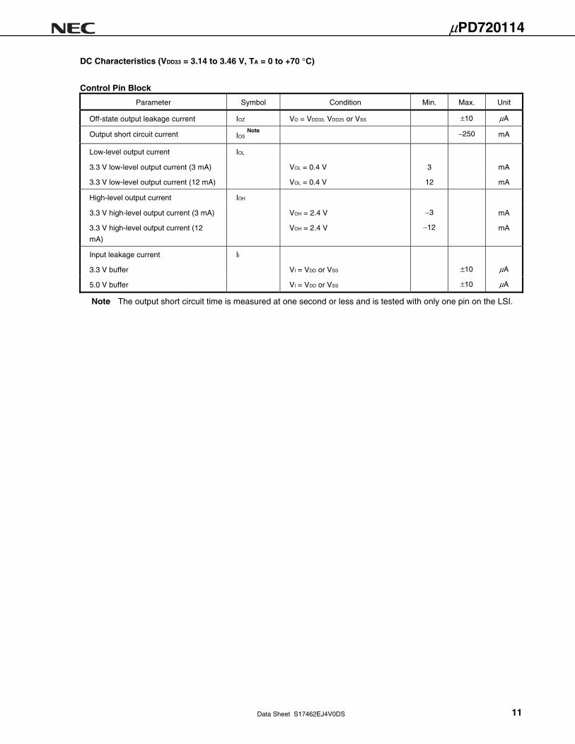
DC Characteristics (VDD33 = 3.14 to 3.46 V, TA = 0 to +70 °C)
Control Pin Block
Parameter Symbol Condition Min. Max. Unit
Off-state output leakage current IOZ VO = VDD33, VDD25 or VSS ±10 μA
Output short circuit current IOS Note
−250 mA
Low-level output current IOL
3.3 V low-level output current (3 mA) VOL = 0.4 V 3 mA
3.3 V low-level output current (12 mA) VOL = 0.4 V 12 mA
High-level output current IOH
3.3 V high-level output current (3 mA) VOH = 2.4 V −3 mA
3.3 V high-level output current (12
mA)
VOH = 2.4 V −12 mA
Input leakage current II
3.3 V buffer VI = VDD or VSS ±10 μA
5.0 V buffer VI = VDD or VSS ±10 μA
Note The output short circuit time is measured at one second or less and is tested with only one pin on the LSI.
Data Sheet S17462EJ4V0DS 12
μPD720114
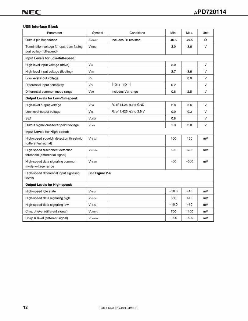
USB Interface Block
Parameter Symbol Conditions Min. Max. Unit
Output pin impedance ZHSDRV Includes RS resistor 40.5 49.5 Ω
Termination voltage for upstream facing
port pullup (full-speed)
VTERM 3.0 3.6 V
Input Levels for Low-/full-speed:
High-level input voltage (drive) VIH 2.0 V
High-level input voltage (floating) VIHZ 2.7 3.6 V
Low-level input voltage VIL 0.8 V
Differential input sensitivity VDI ⏐(D+) − (D−)⏐ 0.2 V
Differential common mode range VCM Includes VDI range 0.8 2.5 V
Output Levels for Low-/full-speed:
High-level output voltage VOH RL of 14.25 kΩ to GND 2.8 3.6 V
Low-level output voltage VOL RL of 1.425 kΩ to 3.6 V 0.0 0.3 V
SE1 VOSE1 0.8 V
Output signal crossover point voltage VCRS 1.3 2.0 V
Input Levels for High-speed:
High-speed squelch detection threshold
(differential signal)
VHSSQ 100 150 mV
High-speed disconnect detection
threshold (differential signal)
VHSDSC 525 625 mV
High-speed data signaling common
mode voltage range
VHSCM −50 +500 mV
High-speed differential input signaling
levels
See Figure 2-4.
Output Levels for High-speed:
High-speed idle state VHSOI −10.0 +10 mV
High-speed data signaling high VHSOH 360 440 mV
High-speed data signaling low VHSOL −10.0 +10 mV
Chirp J level (different signal) VCHIRPJ 700 1100 mV
Chirp K level (different signal) VCHIRPK −900 −500 mV
Data Sheet S17462EJ4V0DS 13
μPD720114
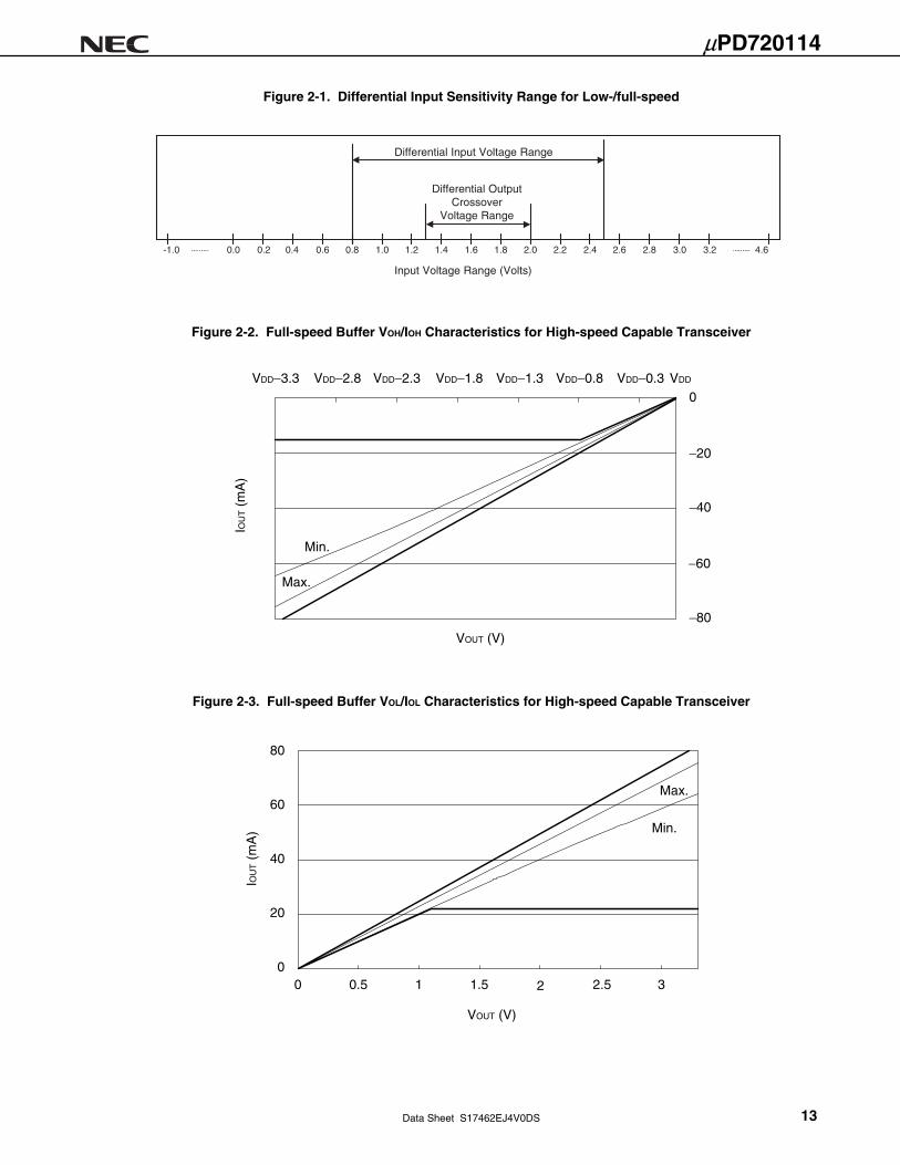
Figure 2-1. Differential Input Sensitivity Range for Low-/full-speed
4.6-1.0
Input Voltage Range (Volts)
Differential Input Voltage Range
Differential OutputCrossover
Voltage Range
0.0 0.2 0.4 0.6 0.8 1.0 1.2 1.4 1.6 1.8 2.0 2.2 2.4 2.6 2.8 3.0 3.2
Figure 2-2. Full-speed Buffer VOH/IOH Characteristics for High-speed Capable Transceiver
Max.
Min.
−80
−60
−40
−20
0VDD−0.3
VOUT (V)
IOU
T (
mA
)
VDD−2.3VDD−3.3 VDD−0.8 VDDVDD−1.3VDD−1.8VDD−2.8
Figure 2-3. Full-speed Buffer VOL/IOL Characteristics for High-speed Capable Transceiver
Max.
Min.
80
60
40
20
00 0.5 1 1.5 2 2.5 3
VOUT (V)
IOU
T (
mA
)
Data Sheet S17462EJ4V0DS 14
μPD720114
Figure 2-4. Receiver Sensitivity for Transceiver at DP/DM
0 VDifferential
+400 mVDifferential
−400 mVDifferential
Unit Interval
Level 1
Level 2
0% 100%
Point 5
Point 2Point 1
Point 3 Point 4
Point 6
Figure 2-5. Receiver Measurement Fixtures
VBUS
D+D-
GND
15.8 Ω +To 50 Ω Inputs of aHigh Speed DifferentialOscilloscope, or 50 ΩOutputs of a High SpeedDifferential Data Generator−
50 ΩCoax
50 ΩCoax
USBConnector
NearestDevice
Test Supply Voltage
15.8 Ω
143 Ω 143 Ω
Data Sheet S17462EJ4V0DS 15
μPD720114
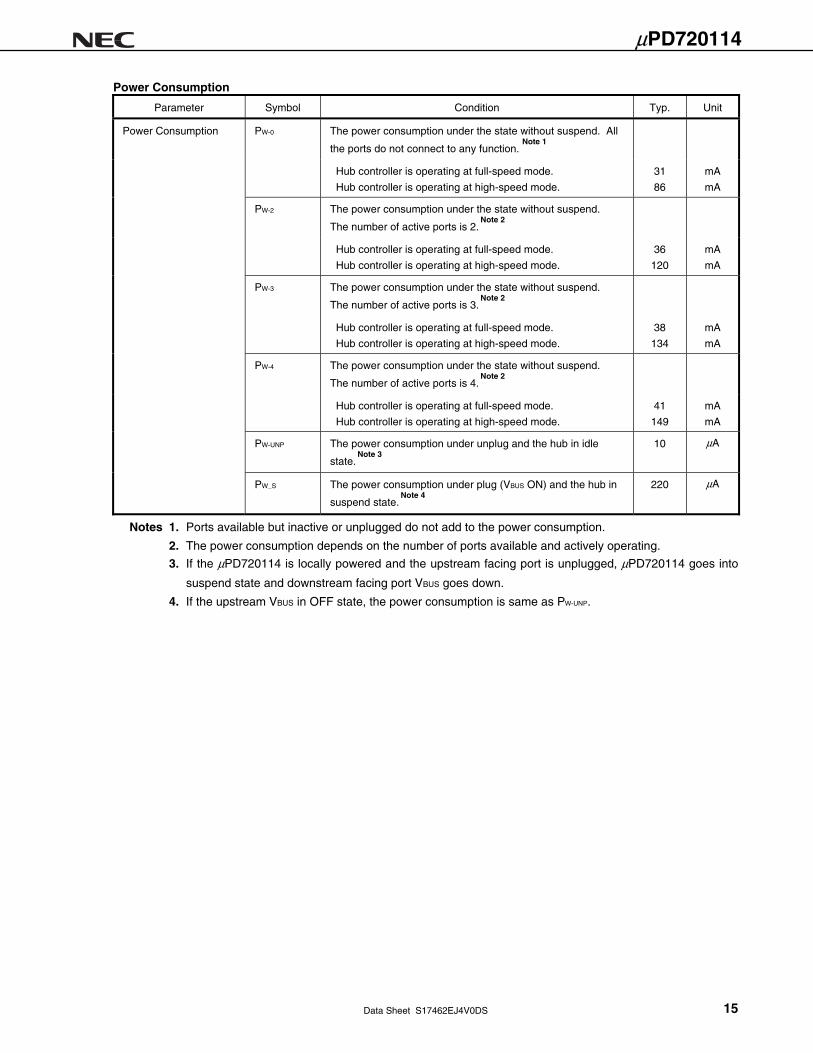
Power Consumption
Parameter Symbol Condition Typ. Unit
Power Consumption PW-0 The power consumption under the state without suspend. All
the ports do not connect to any function. Note 1
Hub controller is operating at full-speed mode.
Hub controller is operating at high-speed mode.
31
86
mA
mA
PW-2 The power consumption under the state without suspend.
The number of active ports is 2. Note 2
Hub controller is operating at full-speed mode.
Hub controller is operating at high-speed mode.
36
120
mA
mA
PW-3 The power consumption under the state without suspend.
The number of active ports is 3. Note 2
Hub controller is operating at full-speed mode.
Hub controller is operating at high-speed mode.
38
134
mA
mA
PW-4 The power consumption under the state without suspend.
The number of active ports is 4. Note 2
Hub controller is operating at full-speed mode.
Hub controller is operating at high-speed mode.
41
149
mA
mA
PW-UNP The power consumption under unplug and the hub in idle
state. Note 3
10 μA
PW_S The power consumption under plug (VBUS ON) and the hub in
suspend state. Note 4
220 μA
Notes 1. Ports available but inactive or unplugged do not add to the power consumption.
2. The power consumption depends on the number of ports available and actively operating.
3. If the μPD720114 is locally powered and the upstream facing port is unplugged, μPD720114 goes into
suspend state and downstream facing port VBUS goes down.
4. If the upstream VBUS in OFF state, the power consumption is same as PW-UNP.
Data Sheet S17462EJ4V0DS 16
μPD720114
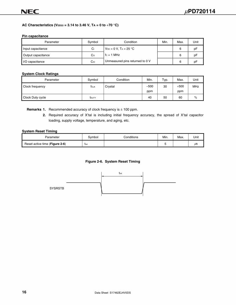
AC Characteristics (VDD33 = 3.14 to 3.46 V, TA = 0 to +70 °C)
Pin capacitance
Parameter Symbol Condition Min. Max. Unit
Input capacitance CI 6 pF
Output capacitance CO 6 pF
I/O capacitance CIO
VDD = 0 V, TA = 25 °C
fC = 1 MHz
Unmeasured pins returned to 0 V 6 pF
System Clock Ratings
Parameter Symbol Condition Min. Typ. Max. Unit
Clock frequency fCLK Crystal −500
ppm
30 +500
ppm
MHz
Clock Duty cycle tDUTY 40 50 60 %
Remarks 1. Recommended accuracy of clock frequency is ± 100 ppm.
2. Required accuracy of X’tal is including initial frequency accuracy, the spread of X’tal capacitor
loading, supply voltage, temperature, and aging, etc.
System Reset Timing
Parameter Symbol Conditions Min. Max. Unit
Reset active time (Figure 2-6) trst 5 μs
Figure 2-6. System Reset Timing
SYSRSTB
trst
Data Sheet S17462EJ4V0DS 17
μPD720114
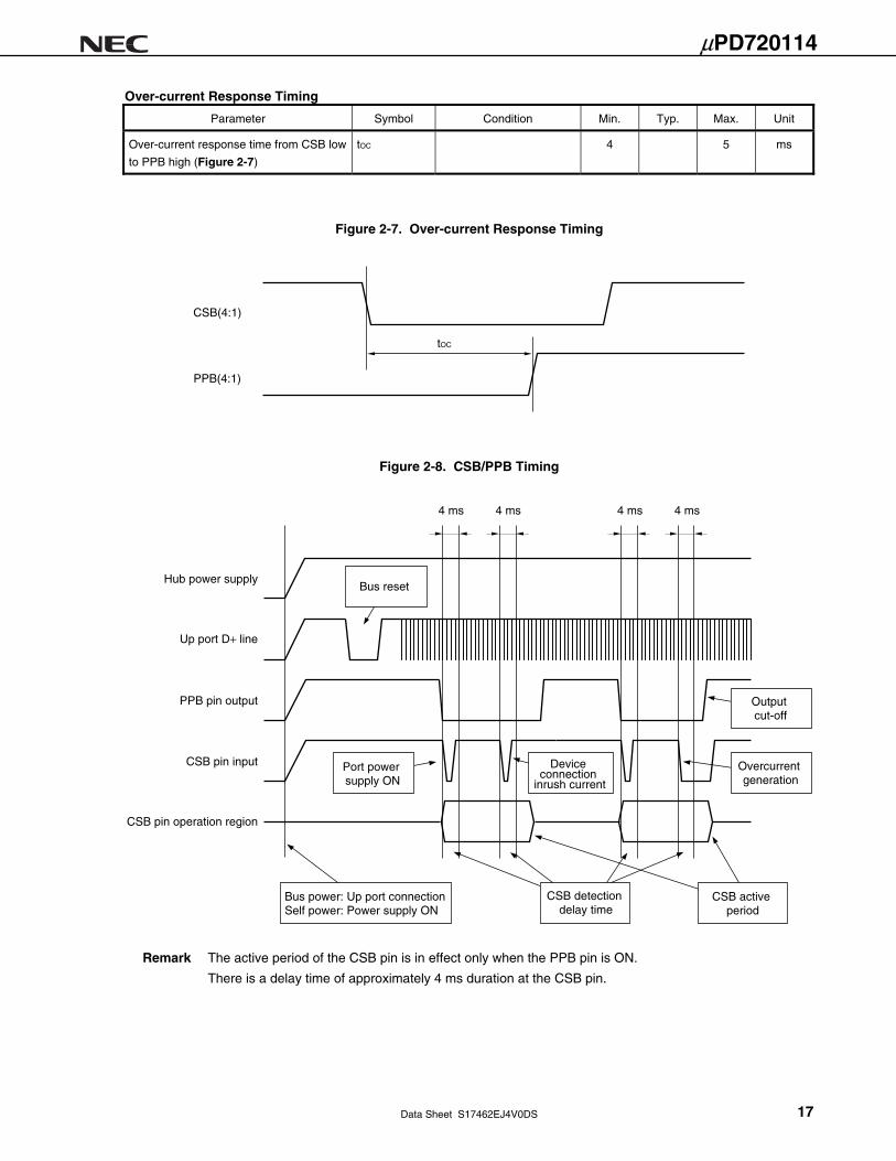
Over-current Response Timing
Parameter Symbol Condition Min. Typ. Max. Unit
Over-current response time from CSB low
to PPB high (Figure 2-7)
tOC 4 5 ms
Figure 2-7. Over-current Response Timing
CSB(4:1)
PPB(4:1)
tOC
Figure 2-8. CSB/PPB Timing
Bus reset
4 ms 4 ms 4 ms 4 ms
Hub power supply
PPB pin output
CSB pin input
CSB pin operation region
Up port D+ line
Port power supply ON
Output cut-off
Overcurrent generation
CSB detection delay time
CSB active period
Device connection
inrush current
Bus power: Up port connectionSelf power: Power supply ON
Remark The active period of the CSB pin is in effect only when the PPB pin is ON.
There is a delay time of approximately 4 ms duration at the CSB pin.
Data Sheet S17462EJ4V0DS 18
μPD720114
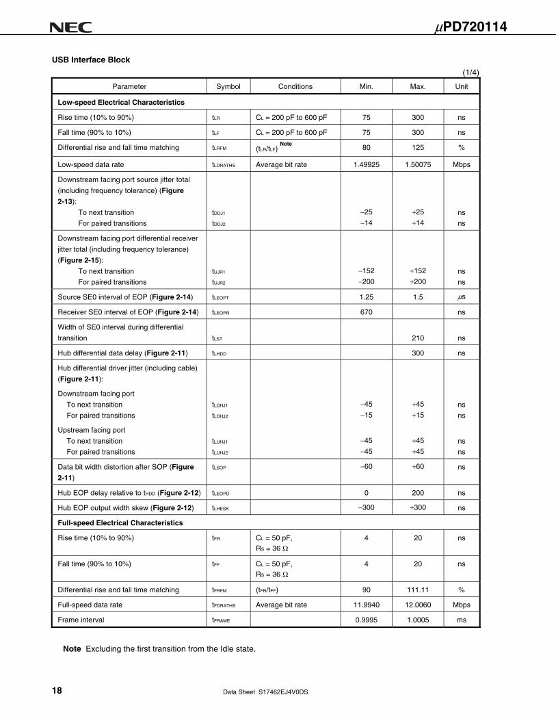
USB Interface Block
(1/4)
Parameter Symbol Conditions Min. Max. Unit
Low-speed Electrical Characteristics
Rise time (10% to 90%) tLR CL = 200 pF to 600 pF 75 300 ns
Fall time (90% to 10%) tLF CL = 200 pF to 600 pF 75 300 ns
Differential rise and fall time matching tLRFM (tLR/tLF) Note
80 125 %
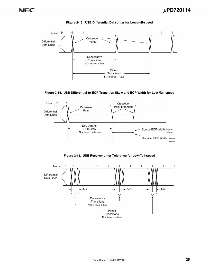
Low-speed data rate tLDRATHS Average bit rate 1.49925 1.50075 Mbps
Downstream facing port source jitter total
(including frequency tolerance) (Figure
2-13):
To next transition
For paired transitions
tDDJ1
tDDJ2
−25
−14
+25
+14
ns
ns
Downstream facing port differential receiver
jitter total (including frequency tolerance)
(Figure 2-15):
To next transition
For paired transitions
tUJR1
tUJR2
−152
−200
+152
+200
ns
ns
Source SE0 interval of EOP (Figure 2-14) tLEOPT 1.25 1.5 μs
Receiver SE0 interval of EOP (Figure 2-14) tLEOPR 670 ns
Width of SE0 interval during differential
transition
tLST
210
ns
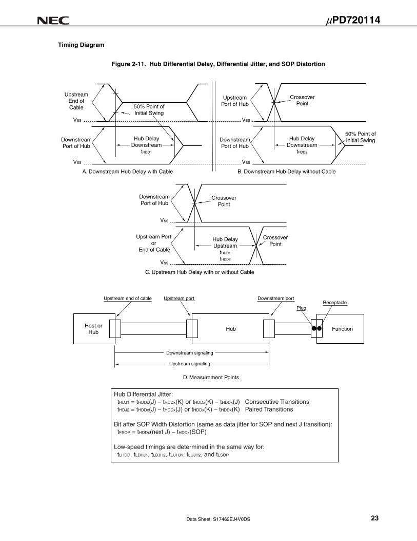
Hub differential data delay (Figure 2-11) tLHDD 300 ns
Hub differential driver jitter (including cable)
(Figure 2-11):
Downstream facing port
To next transition
For paired transitions
Upstream facing port
To next transition
For paired transitions
tLDHJ1
tLDHJ2
tLUHJ1
tLUHJ2
−45
−15
−45
−45
+45
+15
+45
+45
ns
ns
ns
ns
Data bit width distortion after SOP (Figure
2-11)
tLSOP −60 +60 ns
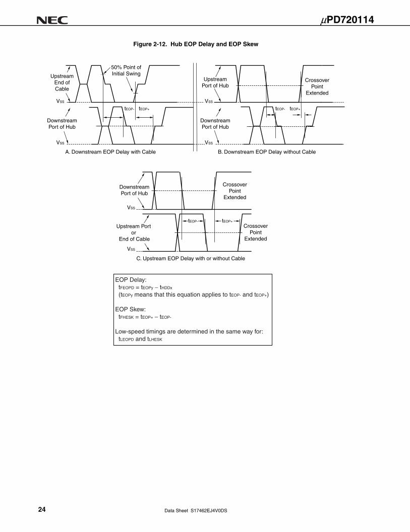
Hub EOP delay relative to tHDD (Figure 2-12) tLEOPD 0 200 ns
Hub EOP output width skew (Figure 2-12) tLHESK −300 +300 ns
Full-speed Electrical Characteristics
Rise time (10% to 90%) tFR CL = 50 pF, RS = 36 Ω
4 20 ns
Fall time (90% to 10%) tFF CL = 50 pF, RS = 36 Ω
4 20 ns
Differential rise and fall time matching tFRFM (tFR/tFF) 90 111.11 %
Full-speed data rate tFDRATHS Average bit rate 11.9940 12.0060 Mbps
Frame interval tFRAME 0.9995 1.0005 ms
Note Excluding the first transition from the Idle state.
Data Sheet S17462EJ4V0DS 19
μPD720114
(2/4)
Parameter Symbol Conditions Min. Max. Unit
Full-speed Electrical Characteristics (Continued)
Consecutive frame interval jitter tRFI No clock adjustment 42 ns
Source jitter total (including frequency
tolerance) (Figure 2-13):
To next transition
For paired transitions
tDJ1
tDJ2
Note
−3.5
−4.0
+3.5
+4.0
ns
ns
Source jitter for differential transition to SE0
transition (Figure 2-14)
tFDEOP −2 +5 ns
Receiver jitter (Figure 2-15):
To Next Transition
For Paired Transitions
tJR1
tJR2
−18.5
−9
+18.5
+9
ns
ns
Source SE0 interval of EOP (Figure 2-14) tFEOPT 160 175 ns
Receiver SE0 interval of EOP (Figure 2-14) tFEOPR 82 ns
Width of SE0 interval during differential
transition
tFST 14 ns
Hub differential data delay (Figure 2-11)
(with cable)
(without cable)
tHDD1
tHDD2
70
44
ns
ns
Hub differential driver jitter (including cable)
(Figure 2-11):
To next transition
For paired transitions
tHDJ1
tHDJ2
−3
−1
+3
+1
ns
ns
Data bit width distortion after SOP (Figure
2-11)
tFSOP −5 +5 ns
Hub EOP delay relative to tHDD (Figure 2-12) tFEOPD 0 15 ns
Hub EOP output width skew (Figure 2-12) tFHESK −15 +15 ns
High-speed Electrical Characteristics
Rise time (10% to 90%) tHSR 500 ps
Fall time (90% to 10%) tHSF 500 ps
Driver waveform See Figure 2-9.
High-speed data rate tHSDRAT 479.760 480.240 Mbps
Microframe interval tHSFRAM 124.9375 125.0625 μs
Consecutive microframe interval difference tHSRFI 4 high-
speed
Bit
times
Data source jitter See Figure 2-9.
Receiver jitter tolerance See Figure 2-4.
Hub data delay (without cable) tHSHDD 36 high-speed+4 ns
Bit
times
Hub data jitter See Figure 2-4, Figure 2-9.
Hub delay variation range tHSHDV 5 high-
speed
Bit
times
Note Excluding the first transition from the Idle state.
Data Sheet S17462EJ4V0DS 20
μPD720114
(3/4)
Parameter Symbol Conditions Min. Max. Unit
Hub Event Timings
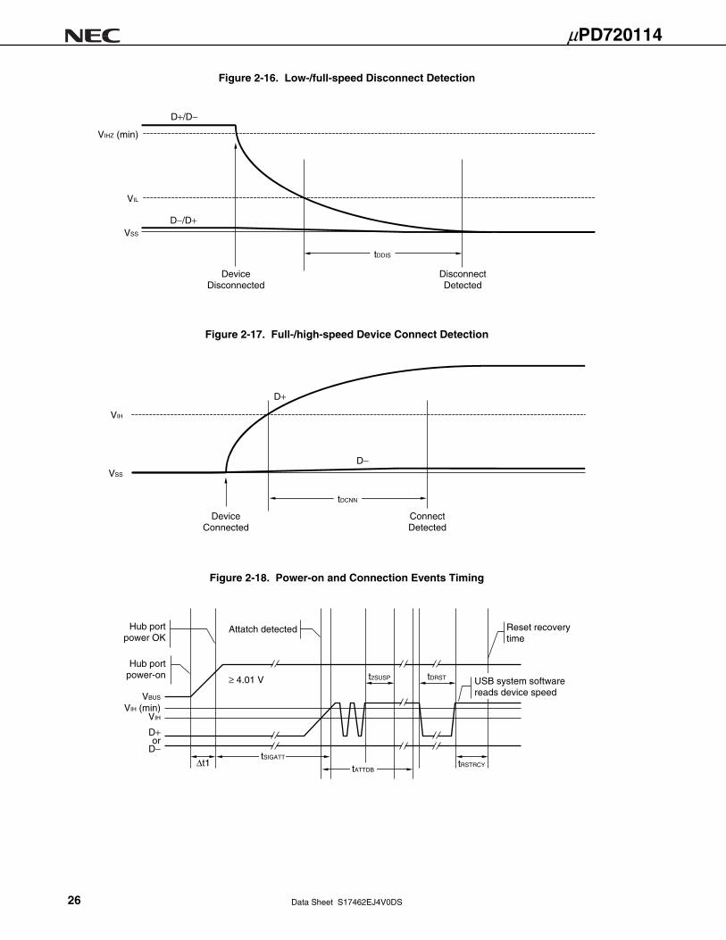
Time to detect a downstream facing port
connect event (Figure 2-17):
Awake hub
Suspended hub
tDCNN
2.5
2.5
2000
12000
μs
μs
Time to detect a disconnect event at a hub’s
downstream facing port (Figure 2-16)
tDDIS 2.0 2.5 μs
Duration of driving resume to a downstream
port (only from a controlling hub)
tDRSMDN 20 ms
Time from detecting downstream resume to
rebroadcast
tURSM 1.0 ms
Duration of driving reset to a downstream
facing port (Figure 2-18)
tDRST Only for a SetPortFeature
(PORT_RESET) request
10 20 ms
Time to detect a long K from upstream tURLK 2.5 100 μs
Time to detect a long SE0 from upstream tURLSE0 2.5 10000 μs
Duration of repeating SE0 upstream (for
low-/full-speed repeater)
tURPSE0 23 FS Bit
times
Inter-packet delay (for high-speed) of
packets traveling in same direction
tHSIPDSD 88 Bit
times
Inter-packet delay (for high-speed) of
packets traveling in opposite direction
tHSIPDOD 8 Bit
times
Inter-packet delay for device/root hub
response with detachable cable for high-
speed
tHSRSPIPD1 192 Bit
times
Time of which a Chirp J or Chirp K must be
continuously detected (filtered) by hub or
device during Reset handshake
tFILT 2.5 μs
Time after end of device Chirp K by which
hub must start driving first Chirp K in the
hub’s chirp sequence
tWTDCH 100 μs
Time for which each individual Chirp J or
Chirp K in the chirp sequence is driven
downstream by hub during reset
tDCHBIT 40 60 μs
Time before end of reset by which a hub
must end its downstream chirp sequence
tDCHSE0 100 500 μs
Time from internal power good to device pulling D+ beyond VIHZ (Figure 2-18)
tSIGATT 100 ms
Debounce interval provided by USB system
software after attach (Figure 2-18)
tATTDB 100 ms
Maximum duration of suspend averaging
interval
tSUSAVGI 1 s
Period of idle bus before device can initiate
resume
tWTRSM 5 ms
Duration of driving resume upstream tDRSMUP 1 15 ms
Data Sheet S17462EJ4V0DS 21
μPD720114
(4/4)
Parameter Symbol Conditions Min. Max. Unit
Hub Event Timings (Continued)
Resume recovery time tRSMRCY Remote-wakeup is
enabled
10 ms
Time to detect a reset from upstream for
non high-speed capable devices
tDETRST 2.5 10000 μs
Reset recovery time (Figure 2-18) tRSTRCY 10 ms
Inter-packet delay for full-speed tIPD 2 Bit
times
Inter-packet delay for device response with
detachable cable for full-speed
tRSPIPD1 6.5 Bit
times
SetAddress() completion time tDSETADDR 50 ms
Time to complete standard request with no
data
tDRQCMPLTND 50 ms
Time to deliver first and subsequent (except
last) data for standard request
tDRETDATA1 500 ms
Time to deliver last data for standard
request
tDRETDATAN 50 ms
Time for which a suspended hub will see a
continuous SE0 on upstream before
beginning the high-speed detection
handshake
tFILTSE0 2.5 μs
Time a hub operating in non-suspended full-
speed will wait after start of SE0 on
upstream before beginning the high-speed
detection handshake
tWTRSTFS 2.5 3000 ms
Time a hub operating in high-speed will wait
after start of SE0 on upstream before
reverting to full-speed
tWTREV 3.0 3.125 ms
Time a hub will wait after reverting to full-
speed before sampling the bus state on
upstream and beginning the high-speed will
wait after start of SE0 on upstream before
reverting to full-speed
tWTRSTHS 100 875 ms
Minimum duration of a Chirp K on upstream
from a hub within the reset protocol
tUCH 1.0 ms
Time after start of SE0 on upstream by
which a hub will complete its Chirp K within
the reset protocol
tUCHEND 7.0 ms
Time between detection of downstream chip
and entering high-speed state
tWTHS 500 μs
Time after end of upstream Chirp at which
hub reverts to full-speed default state if no
downstream Chirp is detected
tWTFS 1.0 2.5 ms
Data Sheet S17462EJ4V0DS 22
μPD720114
Figure 2-9. Transmit Waveform for Transceiver at DP/DM
0 VDifferential
+400 mVDifferential
−400 mVDifferential
Unit Interval
Level 1
Level 2
0% 100%
Point 4Point 3
Point 1 Point 2
Point 5 Point 6
Figure 2-10. Transmitter Measurement Fixtures
VBUS
D+D-
GND
15.8 Ω +To 50 Ω Inputs of aHigh Speed DifferentialOscilloscope, or 50 ΩOutputs of a High SpeedDifferential Data Generator−
50 ΩCoax
50 ΩCoax
USBConnector
NearestDevice
Test Supply Voltage
15.8 Ω
143 Ω 143 Ω
Data Sheet S17462EJ4V0DS 23
μPD720114
Timing Diagram
Figure 2-11. Hub Differential Delay, Differential Jitter, and SOP Distortion
C. Upstream Hub Delay with or without Cable
D. Measurement Points
50% Point ofInitial Swing
50% Point ofInitial Swing
UpstreamEnd ofCable
UpstreamPort of Hub
DownstreamPort of Hub
DownstreamPort of Hub
DownstreamPort of Hub
Upstream Port or
End of Cable
A. Downstream Hub Delay with Cable B. Downstream Hub Delay without Cable
Hub DelayDownstream
tHDD1
Hub DelayUpstream
tHDD1
tHDD2
CrossoverPoint
CrossoverPoint
CrossoverPoint
VSS
Hub Differential Jitter: tHDJ1 = tHDDx(J) − tHDDx(K) or tHDDx(K) − tHDDx(J) Consecutive Transitions tHDJ2 = tHDDx(J) − tHDDx(J) or tHDDx(K) − tHDDx(K) Paired Transitions
Bit after SOP Width Distortion (same as data jitter for SOP and next J transition): tFSOP = tHDDx(next J) − tHDDx(SOP)
Low-speed timings are determined in the same way for: tLHDD, tLDHJ1, tLDJH2, tLUHJ1, tLUJH2, and tLSOP
Host orHub
Hub Function
Upstream end of cable Upstream port Downstream port
Downstream signaling
Upstream signaling
PlugReceptacle
Hub DelayDownstream
tHDD2
VSS
VSS
VSS
VSS
VSS
Data Sheet S17462EJ4V0DS 24
μPD720114
Figure 2-12. Hub EOP Delay and EOP Skew
tEOP- tEOP+
tEOP- tEOP+ tEOP- tEOP+
C. Upstream EOP Delay with or without Cable
UpstreamEnd ofCable
UpstreamPort of Hub
DownstreamPort of Hub
DownstreamPort of Hub
DownstreamPort of Hub
Upstream Port or
End of Cable
A. Downstream EOP Delay with Cable B. Downstream EOP Delay without Cable
VSS
VSS
VSS
VSS
VSS
VSS
50% Point ofInitial Swing
CrossoverPoint
Extended
CrossoverPoint
Extended
CrossoverPoint
Extended
EOP Delay: tFEOPD = tEOPy − tHDDx
(tEOPy means that this equation applies to tEOP- and tEOP+)
EOP Skew: tFHESK = tEOP+ − tEOP-
Low-speed timings are determined in the same way for: tLEOPD and tLHESK
Data Sheet S17462EJ4V0DS 25
μPD720114
Figure 2-13. USB Differential Data Jitter for Low-/full-speed
tPERIOD
DifferentialData Lines
CrossoverPoints
ConsecutiveTransitions
N × tPERIOD + txDJ1
PairedTransitions
N × tPERIOD + txDJ2
Figure 2-14. USB Differential-to-EOP Transition Skew and EOP Width for Low-/full-speed
tPERIOD
DifferentialData Lines
CrossoverPoint
CrossoverPoint Extended
Source EOP Width: tFEOPT
Receiver EOP Width: tFEOPR
tLEOPT
tLEOPR
Diff. Data-to-SE0 Skew
N × tPERIOD + txDEOP
Figure 2-15. USB Receiver Jitter Tolerance for Low-/full-speed
DifferentialData Lines
tPERIOD
txJR txJR1 txJR2
ConsecutiveTransitions
N × tPERIOD + txJR1
PairedTransitions
N × tPERIOD + txJR2
Data Sheet S17462EJ4V0DS 26
μPD720114
Figure 2-16. Low-/full-speed Disconnect Detection
D−/D+
D+/D−
VIHZ (min)
VIL
VSS
DeviceDisconnected
DisconnectDetected
tDDIS
Figure 2-17. Full-/high-speed Device Connect Detection
VIH
VSS
DeviceConnected
ConnectDetected
D−
D+
tDCNN
Figure 2-18. Power-on and Connection Events Timing
tSIGATTΔt1 tRSTRCY
D+or
D−
Hub portpower OK
Attatch detected Reset recoverytime
USB system softwarereads device speed
≥ 4.01 V
VBUS
VIH (min)VIH
Hub portpower-on
tATTDB
t2SUSP tDRST
Data Sheet S17462EJ4V0DS 27
μPD720114
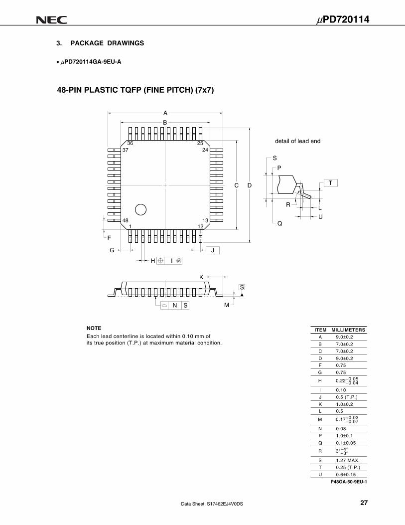
3. PACKAGE DRAWINGS
• μPD720114GA-9EU-A
NOTE
Each lead centerline is located within 0.10 mm ofits true position (T.P.) at maximum material condition.
A
S
P
B
C D
M
G
H
K
I
J
R
detail of lead end
F
48-PIN PLASTIC TQFP (FINE PITCH) (7x7)
ITEM MILLIMETERS
A 9.0±0.2
B 7.0±0.2
F 0.75
G
H
0.75
C 7.0±0.2
D 9.0±0.2
P48GA-50-9EU-1
I 0.10
L 0.5
J 0.5 (T.P.)
K 1.0±0.2
M
3637 24
481
1312
25
SN
S
Q
L
T
U
0.22+0.05−0.04
M
N 0.08
P 1.0±0.1
Q 0.1±0.05
T 0.25 (T.P.)
U 0.6±0.15
0.17+0.03−0.07
R
S 1.27 MAX.
3°+4°−3°
Data Sheet S17462EJ4V0DS 28
μPD720114
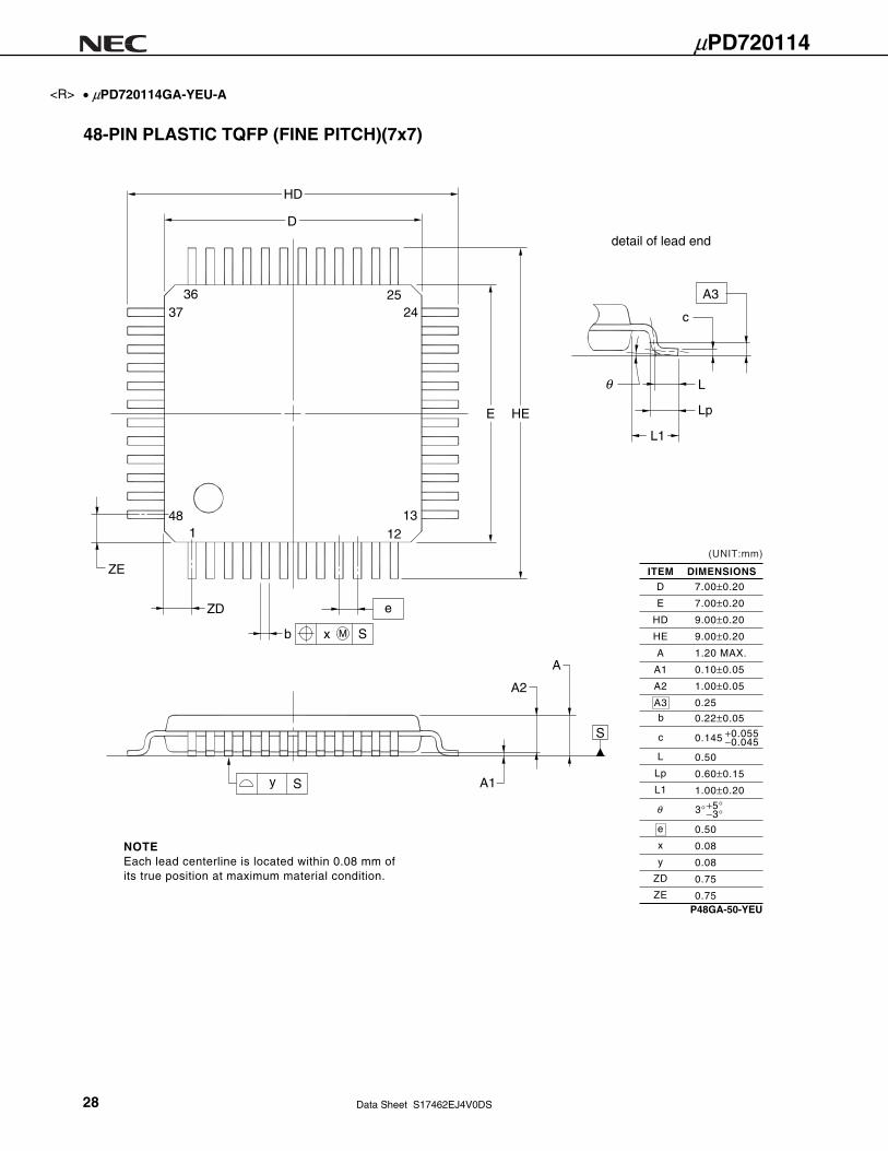
• μPD720114GA-YEU-A
Sy
e
Sxb M
θ L
c
Lp
HD
HE
ZD
ZE
L1
A1
A2
A
D
E
A3
S 0.145 +0.055−0.045
(UNIT:mm)
ITEM DIMENSIONS
D
E
HD
HE
A
A1
A2
A3
7.00±0.20
7.00±0.20
9.00±0.20
9.00±0.20
1.20 MAX.
0.10±0.05
1.00±0.05
0.25
c
θ
e
x
y
ZD
ZE
0.50
0.08
0.08
0.75
0.75
L
Lp
L1
0.50
0.60±0.15
1.00±0.20
P48GA-50-YEU
3°+5°−3°
NOTEEach lead centerline is located within 0.08 mm ofits true position at maximum material condition.
detail of lead end
48-PIN PLASTIC TQFP (FINE PITCH)(7x7)
0.22±0.05b
12
24
148 13
2537
36
<R>
Data Sheet S17462EJ4V0DS 29
μPD720114
4. RECOMMENDED SOLDERING CONDITIONS
The μPD720114 should be soldered and mounted under the following recommended conditions.
For soldering methods and conditions other than those recommended below, contact an NEC Electronics sales
representative.
For technical information, see the following website.
Semiconductor Device Mount Manual (http://www.necel.com/pkg/en/mount/index.html)
• μPD720114GA-9EU-A: 48-pin plastic TQFP (Fine pitch) (7 × 7)
• μPD720114GA-YEU-A: 48-pin plastic TQFP (Fine pitch) (7 × 7)
Soldering Method Soldering Conditions Symbol
Infrared reflow Peak package’s surface temperature: 260 °C, Reflow time: 60 seconds or less
(220 °C or higher), Maximum allowable number of reflow processes: 3,
Exposure limit Note
: 7 days (10 to 72 hours pre-backing is required at 125C°
afterwards),
Flux: Rosin flux with low chlorine (0.2 Wt% or below) recommended.
<Caution>
Non-heat-resistant trays, such as magazine and taping trays, cannot be baked
before unpacking.
IR60-107-3
Partial heating method Pin temperature: 300°C or below,
Heat time: 3 seconds or less (per each side of the device) ,
Flux: Rosin flux with low chlorine (0.2 Wt% or below) recommended.
–
Note The Maximum number of days during which the product can be stored at a temperature of 5 to 25°C and a
relative humidity of 20 to 65% after dry-pack package is opened.

Data Sheet S17462EJ4V0DS 30
μPD720114
[MEMO]
Data Sheet S17462EJ4V0DS 31
μPD720114
1
2
3
4
VOLTAGE APPLICATION WAVEFORM AT INPUT PIN
Waveform distortion due to input noise or a reflected wave may cause malfunction. If the input of the
CMOS device stays in the area between VIL (MAX) and VIH (MIN) due to noise, etc., the device may
malfunction. Take care to prevent chattering noise from entering the device when the input level is fixed,
and also in the transition period when the input level passes through the area between VIL (MAX) and
VIH (MIN).
HANDLING OF UNUSED INPUT PINS
Unconnected CMOS device inputs can be cause of malfunction. If an input pin is unconnected, it is
possible that an internal input level may be generated due to noise, etc., causing malfunction. CMOS
devices behave differently than Bipolar or NMOS devices. Input levels of CMOS devices must be fixed
high or low by using pull-up or pull-down circuitry. Each unused pin should be connected to VDD or GND
via a resistor if there is a possibility that it will be an output pin. All handling related to unused pins must
be judged separately for each device and according to related specifications governing the device.
PRECAUTION AGAINST ESD
A strong electric field, when exposed to a MOS device, can cause destruction of the gate oxide and
ultimately degrade the device operation. Steps must be taken to stop generation of static electricity as
much as possible, and quickly dissipate it when it has occurred. Environmental control must be
adequate. When it is dry, a humidifier should be used. It is recommended to avoid using insulators that
easily build up static electricity. Semiconductor devices must be stored and transported in an anti-static
container, static shielding bag or conductive material. All test and measurement tools including work
benches and floors should be grounded. The operator should be grounded using a wrist strap.
Semiconductor devices must not be touched with bare hands. Similar precautions need to be taken for
PW boards with mounted semiconductor devices.
STATUS BEFORE INITIALIZATION
Power-on does not necessarily define the initial status of a MOS device. Immediately after the power
source is turned ON, devices with reset functions have not yet been initialized. Hence, power-on does
not guarantee output pin levels, I/O settings or contents of registers. A device is not initialized until the
reset signal is received. A reset operation must be executed immediately after power-on for devices
with reset functions.
POWER ON/OFF SEQUENCE
In the case of a device that uses different power supplies for the internal operation and external
interface, as a rule, switch on the external power supply after switching on the internal power supply.
When switching the power supply off, as a rule, switch off the external power supply and then the
internal power supply. Use of the reverse power on/off sequences may result in the application of an
overvoltage to the internal elements of the device, causing malfunction and degradation of internal
elements due to the passage of an abnormal current.
The correct power on/off sequence must be judged separately for each device and according to related
specifications governing the device.
INPUT OF SIGNAL DURING POWER OFF STATE
Do not input signals or an I/O pull-up power supply while the device is not powered. The current
injection that results from input of such a signal or I/O pull-up power supply may cause malfunction and
the abnormal current that passes in the device at this time may cause degradation of internal elements.
Input of signals during the power off state must be judged separately for each device and according to
related specifications governing the device.
NOTES FOR CMOS DEVICES
5
6
μPD720114
ECOUSB is a trademark of NEC Electronics Corporation.
The information in this document is current as of June, 2007. The information is subject to change without notice. For actual design-in, refer to the latest publications of NEC Electronics data sheets or data books, etc., for the most up-to-date specifications of NEC Electronics products. Not all products and/or types are available in every country. Please check with an NEC Electronics sales representative for availability and additional information.No part of this document may be copied or reproduced in any form or by any means without the prior written consent of NEC Electronics. NEC Electronics assumes no responsibility for any errors that may appear in this document.NEC Electronics does not assume any liability for infringement of patents, copyrights or other intellectual property rights of third parties by or arising from the use of NEC Electronics products listed in this document or any other liability arising from the use of such products. No license, express, implied or otherwise, is granted under any patents, copyrights or other intellectual property rights of NEC Electronics or others.Descriptions of circuits, software and other related information in this document are provided for illustrative purposes in semiconductor product operation and application examples. The incorporation of these circuits, software and information in the design of a customer's equipment shall be done under the full responsibility of the customer. NEC Electronics assumes no responsibility for any losses incurred by customers or third parties arising from the use of these circuits, software and information.While NEC Electronics endeavors to enhance the quality, reliability and safety of NEC Electronics products, customers agree and acknowledge that the possibility of defects thereof cannot be eliminated entirely. To minimize risks of damage to property or injury (including death) to persons arising from defects in NEC Electronics products, customers must incorporate sufficient safety measures in their design, such as redundancy, fire-containment and anti-failure features.NEC Electronics products are classified into the following three quality grades: "Standard", "Special" and "Specific". The "Specific" quality grade applies only to NEC Electronics products developed based on a customer-designated "quality assurance program" for a specific application. The recommended applications of an NEC Electronics product depend on its quality grade, as indicated below. Customers must check the quality grade of each NEC Electronics product before using it in a particular application.
The quality grade of NEC Electronics products is "Standard" unless otherwise expressly specified in NEC Electronics data sheets or data books, etc. If customers wish to use NEC Electronics products in applications not intended by NEC Electronics, they must contact an NEC Electronics sales representative in advance to determine NEC Electronics' willingness to support a given application.
(Note)
•
•
•
•
•
•
M8E 02. 11-1
(1)
(2)
"NEC Electronics" as used in this statement means NEC Electronics Corporation and also includes its majority-owned subsidiaries."NEC Electronics products" means any product developed or manufactured by or for NEC Electronics (as defined above).
Computers, office equipment, communications equipment, test and measurement equipment, audioand visual equipment, home electronic appliances, machine tools, personal electronic equipmentand industrial robots.Transportation equipment (automobiles, trains, ships, etc.), traffic control systems, anti-disastersystems, anti-crime systems, safety equipment and medical equipment (not specifically designedfor life support).Aircraft, aerospace equipment, submersible repeaters, nuclear reactor control systems, lifesupport systems and medical equipment for life support, etc.
"Standard":
"Special":
"Specific":