Embed Size (px)
Citation preview
March 2013
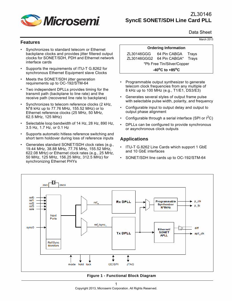
ZL30146 SyncE SONET/SDH Line Card PLL
Data Sheet
Ordering Information ZL30146GGG 64 Pin CABGA Trays ZL30146GGG2 64 Pin CABGA* Trays
*Pb Free Tin/Silver/Copper-40oC to +85oC
Features• Synchronizes to standard telecom or Ethernet
backplane clocks and provides jitter filtered output clocks for SONET/SDH, PDH and Ethernet network interface cards
• Supports the requirements of ITU-T G.8262 for synchronous Ethernet Equipment slave Clocks
• Meets the SONET/SDH jitter generation requirements up to OC-192/STM-64
• Two independent DPLLs provides timing for the transmit path (backplane to line rate) and the receive path (recovered line rate to backplane)
• Synchronizes to telecom reference clocks (2 kHz, N*8 kHz up to 77.76 MHz, 155.52 MHz) or to Ethernet reference clocks (25 MHz, 50 MHz, 62.5 MHz, 125 MHz)
• Selectable loop bandwidth of 14 Hz, 28 Hz, 890 Hz, 3.5 Hz, 1.7 Hz, or 0.1 Hz
• Supports automatic hitless reference switching and short term holdover during loss of reference inputs
• Generates standard SONET/SDH clock rates (e.g., 19.44 MHz, 38.88 MHz, 77.76 MHz, 155.52 MHz, 622.08 MHz) or Ethernet clock rates (e.g., 25 MHz, 50 MHz, 125 MHz, 156.25 MHz, 312.5 MHz) for synchronizing Ethernet PHYs
1Copyright 2013, Microsemi Cor
Figure 1 - Funct
• Programmable output synthesizer to generate telecom clock frequencies from any multiple of 8 kHz up to 100 MHz (e.g., T1/E1, DS3/E3)
• Generates several styles of output frame pulse with selectable pulse width, polarity, and frequency
• Configurable input to output delay and output to output phase alignment
• Configurable through a serial interface (SPI or I2C)
• DPLLs can be configured to provide synchronous or asynchronous clock outputs
Applications• ITU-T G.8262 Line Cards which support 1 GbE
and 10 GbE interfaces
• SONET/SDH line cards up to OC-192/STM-64
poration. All Rights Reserved.
ional Block Diagram
ZL30146 Data Sheet
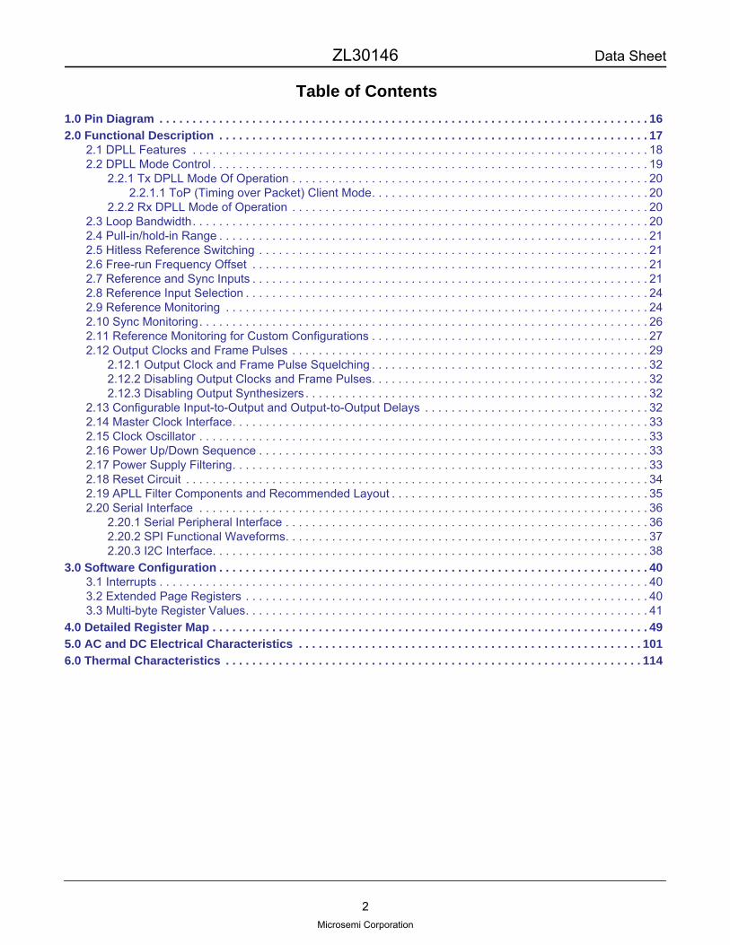
Table of Contents
2Microsemi Corporation
1.0 Pin Diagram . . . . . . . . . . . . . . . . . . . . . . . . . . . . . . . . . . . . . . . . . . . . . . . . . . . . . . . . . . . . . . . . . . . . . . . . . . 162.0 Functional Description . . . . . . . . . . . . . . . . . . . . . . . . . . . . . . . . . . . . . . . . . . . . . . . . . . . . . . . . . . . . . . . . . 17
2.1 DPLL Features . . . . . . . . . . . . . . . . . . . . . . . . . . . . . . . . . . . . . . . . . . . . . . . . . . . . . . . . . . . . . . . . . . . . . 182.2 DPLL Mode Control . . . . . . . . . . . . . . . . . . . . . . . . . . . . . . . . . . . . . . . . . . . . . . . . . . . . . . . . . . . . . . . . . . 19
2.2.1 Tx DPLL Mode Of Operation . . . . . . . . . . . . . . . . . . . . . . . . . . . . . . . . . . . . . . . . . . . . . . . . . . . . . . 202.2.1.1 ToP (Timing over Packet) Client Mode. . . . . . . . . . . . . . . . . . . . . . . . . . . . . . . . . . . . . . . . . . 20
2.2.2 Rx DPLL Mode of Operation . . . . . . . . . . . . . . . . . . . . . . . . . . . . . . . . . . . . . . . . . . . . . . . . . . . . . . 202.3 Loop Bandwidth. . . . . . . . . . . . . . . . . . . . . . . . . . . . . . . . . . . . . . . . . . . . . . . . . . . . . . . . . . . . . . . . . . . . . 202.4 Pull-in/hold-in Range . . . . . . . . . . . . . . . . . . . . . . . . . . . . . . . . . . . . . . . . . . . . . . . . . . . . . . . . . . . . . . . . . 212.5 Hitless Reference Switching . . . . . . . . . . . . . . . . . . . . . . . . . . . . . . . . . . . . . . . . . . . . . . . . . . . . . . . . . . . 212.6 Free-run Frequency Offset . . . . . . . . . . . . . . . . . . . . . . . . . . . . . . . . . . . . . . . . . . . . . . . . . . . . . . . . . . . . 212.7 Reference and Sync Inputs . . . . . . . . . . . . . . . . . . . . . . . . . . . . . . . . . . . . . . . . . . . . . . . . . . . . . . . . . . . . 212.8 Reference Input Selection . . . . . . . . . . . . . . . . . . . . . . . . . . . . . . . . . . . . . . . . . . . . . . . . . . . . . . . . . . . . . 242.9 Reference Monitoring . . . . . . . . . . . . . . . . . . . . . . . . . . . . . . . . . . . . . . . . . . . . . . . . . . . . . . . . . . . . . . . . 242.10 Sync Monitoring. . . . . . . . . . . . . . . . . . . . . . . . . . . . . . . . . . . . . . . . . . . . . . . . . . . . . . . . . . . . . . . . . . . . 262.11 Reference Monitoring for Custom Configurations . . . . . . . . . . . . . . . . . . . . . . . . . . . . . . . . . . . . . . . . . . 272.12 Output Clocks and Frame Pulses . . . . . . . . . . . . . . . . . . . . . . . . . . . . . . . . . . . . . . . . . . . . . . . . . . . . . . 29
2.12.1 Output Clock and Frame Pulse Squelching . . . . . . . . . . . . . . . . . . . . . . . . . . . . . . . . . . . . . . . . . . 322.12.2 Disabling Output Clocks and Frame Pulses. . . . . . . . . . . . . . . . . . . . . . . . . . . . . . . . . . . . . . . . . . 322.12.3 Disabling Output Synthesizers . . . . . . . . . . . . . . . . . . . . . . . . . . . . . . . . . . . . . . . . . . . . . . . . . . . . 32
2.13 Configurable Input-to-Output and Output-to-Output Delays . . . . . . . . . . . . . . . . . . . . . . . . . . . . . . . . . . 322.14 Master Clock Interface. . . . . . . . . . . . . . . . . . . . . . . . . . . . . . . . . . . . . . . . . . . . . . . . . . . . . . . . . . . . . . . 332.15 Clock Oscillator . . . . . . . . . . . . . . . . . . . . . . . . . . . . . . . . . . . . . . . . . . . . . . . . . . . . . . . . . . . . . . . . . . . . 332.16 Power Up/Down Sequence . . . . . . . . . . . . . . . . . . . . . . . . . . . . . . . . . . . . . . . . . . . . . . . . . . . . . . . . . . . 332.17 Power Supply Filtering. . . . . . . . . . . . . . . . . . . . . . . . . . . . . . . . . . . . . . . . . . . . . . . . . . . . . . . . . . . . . . . 332.18 Reset Circuit . . . . . . . . . . . . . . . . . . . . . . . . . . . . . . . . . . . . . . . . . . . . . . . . . . . . . . . . . . . . . . . . . . . . . . 342.19 APLL Filter Components and Recommended Layout . . . . . . . . . . . . . . . . . . . . . . . . . . . . . . . . . . . . . . . 352.20 Serial Interface . . . . . . . . . . . . . . . . . . . . . . . . . . . . . . . . . . . . . . . . . . . . . . . . . . . . . . . . . . . . . . . . . . . . 36
2.20.1 Serial Peripheral Interface . . . . . . . . . . . . . . . . . . . . . . . . . . . . . . . . . . . . . . . . . . . . . . . . . . . . . . . 362.20.2 SPI Functional Waveforms. . . . . . . . . . . . . . . . . . . . . . . . . . . . . . . . . . . . . . . . . . . . . . . . . . . . . . . 372.20.3 I2C Interface. . . . . . . . . . . . . . . . . . . . . . . . . . . . . . . . . . . . . . . . . . . . . . . . . . . . . . . . . . . . . . . . . . 38
3.0 Software Configuration . . . . . . . . . . . . . . . . . . . . . . . . . . . . . . . . . . . . . . . . . . . . . . . . . . . . . . . . . . . . . . . . . 403.1 Interrupts . . . . . . . . . . . . . . . . . . . . . . . . . . . . . . . . . . . . . . . . . . . . . . . . . . . . . . . . . . . . . . . . . . . . . . . . . . 403.2 Extended Page Registers . . . . . . . . . . . . . . . . . . . . . . . . . . . . . . . . . . . . . . . . . . . . . . . . . . . . . . . . . . . . . 403.3 Multi-byte Register Values. . . . . . . . . . . . . . . . . . . . . . . . . . . . . . . . . . . . . . . . . . . . . . . . . . . . . . . . . . . . . 41
4.0 Detailed Register Map . . . . . . . . . . . . . . . . . . . . . . . . . . . . . . . . . . . . . . . . . . . . . . . . . . . . . . . . . . . . . . . . . . 495.0 AC and DC Electrical Characteristics . . . . . . . . . . . . . . . . . . . . . . . . . . . . . . . . . . . . . . . . . . . . . . . . . . . . 1016.0 Thermal Characteristics . . . . . . . . . . . . . . . . . . . . . . . . . . . . . . . . . . . . . . . . . . . . . . . . . . . . . . . . . . . . . . . 114
ZL30146 Data Sheet
List of Figures
5Microsemi Corporation
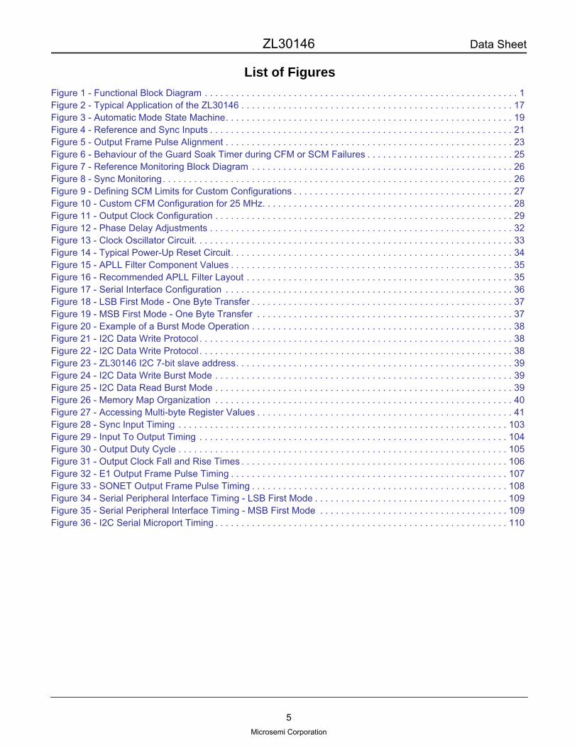
Figure 1 - Functional Block Diagram . . . . . . . . . . . . . . . . . . . . . . . . . . . . . . . . . . . . . . . . . . . . . . . . . . . . . . . . . . . . 1Figure 2 - Typical Application of the ZL30146 . . . . . . . . . . . . . . . . . . . . . . . . . . . . . . . . . . . . . . . . . . . . . . . . . . . . 17Figure 3 - Automatic Mode State Machine. . . . . . . . . . . . . . . . . . . . . . . . . . . . . . . . . . . . . . . . . . . . . . . . . . . . . . . 19Figure 4 - Reference and Sync Inputs . . . . . . . . . . . . . . . . . . . . . . . . . . . . . . . . . . . . . . . . . . . . . . . . . . . . . . . . . . 21Figure 5 - Output Frame Pulse Alignment . . . . . . . . . . . . . . . . . . . . . . . . . . . . . . . . . . . . . . . . . . . . . . . . . . . . . . . 23Figure 6 - Behaviour of the Guard Soak Timer during CFM or SCM Failures . . . . . . . . . . . . . . . . . . . . . . . . . . . . 25Figure 7 - Reference Monitoring Block Diagram . . . . . . . . . . . . . . . . . . . . . . . . . . . . . . . . . . . . . . . . . . . . . . . . . . 26Figure 8 - Sync Monitoring. . . . . . . . . . . . . . . . . . . . . . . . . . . . . . . . . . . . . . . . . . . . . . . . . . . . . . . . . . . . . . . . . . . 26Figure 9 - Defining SCM Limits for Custom Configurations . . . . . . . . . . . . . . . . . . . . . . . . . . . . . . . . . . . . . . . . . . 27Figure 10 - Custom CFM Configuration for 25 MHz. . . . . . . . . . . . . . . . . . . . . . . . . . . . . . . . . . . . . . . . . . . . . . . . 28Figure 11 - Output Clock Configuration . . . . . . . . . . . . . . . . . . . . . . . . . . . . . . . . . . . . . . . . . . . . . . . . . . . . . . . . . 29Figure 12 - Phase Delay Adjustments . . . . . . . . . . . . . . . . . . . . . . . . . . . . . . . . . . . . . . . . . . . . . . . . . . . . . . . . . . 32Figure 13 - Clock Oscillator Circuit. . . . . . . . . . . . . . . . . . . . . . . . . . . . . . . . . . . . . . . . . . . . . . . . . . . . . . . . . . . . . 33Figure 14 - Typical Power-Up Reset Circuit. . . . . . . . . . . . . . . . . . . . . . . . . . . . . . . . . . . . . . . . . . . . . . . . . . . . . . 34Figure 15 - APLL Filter Component Values . . . . . . . . . . . . . . . . . . . . . . . . . . . . . . . . . . . . . . . . . . . . . . . . . . . . . . 35Figure 16 - Recommended APLL Filter Layout . . . . . . . . . . . . . . . . . . . . . . . . . . . . . . . . . . . . . . . . . . . . . . . . . . . 35Figure 17 - Serial Interface Configuration . . . . . . . . . . . . . . . . . . . . . . . . . . . . . . . . . . . . . . . . . . . . . . . . . . . . . . . 36Figure 18 - LSB First Mode - One Byte Transfer . . . . . . . . . . . . . . . . . . . . . . . . . . . . . . . . . . . . . . . . . . . . . . . . . . 37Figure 19 - MSB First Mode - One Byte Transfer . . . . . . . . . . . . . . . . . . . . . . . . . . . . . . . . . . . . . . . . . . . . . . . . . 37Figure 20 - Example of a Burst Mode Operation . . . . . . . . . . . . . . . . . . . . . . . . . . . . . . . . . . . . . . . . . . . . . . . . . . 38Figure 21 - I2C Data Write Protocol . . . . . . . . . . . . . . . . . . . . . . . . . . . . . . . . . . . . . . . . . . . . . . . . . . . . . . . . . . . . 38Figure 22 - I2C Data Write Protocol . . . . . . . . . . . . . . . . . . . . . . . . . . . . . . . . . . . . . . . . . . . . . . . . . . . . . . . . . . . . 38Figure 23 - ZL30146 I2C 7-bit slave address. . . . . . . . . . . . . . . . . . . . . . . . . . . . . . . . . . . . . . . . . . . . . . . . . . . . . 39Figure 24 - I2C Data Write Burst Mode . . . . . . . . . . . . . . . . . . . . . . . . . . . . . . . . . . . . . . . . . . . . . . . . . . . . . . . . . 39Figure 25 - I2C Data Read Burst Mode . . . . . . . . . . . . . . . . . . . . . . . . . . . . . . . . . . . . . . . . . . . . . . . . . . . . . . . . . 39Figure 26 - Memory Map Organization . . . . . . . . . . . . . . . . . . . . . . . . . . . . . . . . . . . . . . . . . . . . . . . . . . . . . . . . . 40Figure 27 - Accessing Multi-byte Register Values . . . . . . . . . . . . . . . . . . . . . . . . . . . . . . . . . . . . . . . . . . . . . . . . . 41Figure 28 - Sync Input Timing . . . . . . . . . . . . . . . . . . . . . . . . . . . . . . . . . . . . . . . . . . . . . . . . . . . . . . . . . . . . . . . 103Figure 29 - Input To Output Timing . . . . . . . . . . . . . . . . . . . . . . . . . . . . . . . . . . . . . . . . . . . . . . . . . . . . . . . . . . . 104Figure 30 - Output Duty Cycle . . . . . . . . . . . . . . . . . . . . . . . . . . . . . . . . . . . . . . . . . . . . . . . . . . . . . . . . . . . . . . . 105Figure 31 - Output Clock Fall and Rise Times . . . . . . . . . . . . . . . . . . . . . . . . . . . . . . . . . . . . . . . . . . . . . . . . . . . 106Figure 32 - E1 Output Frame Pulse Timing . . . . . . . . . . . . . . . . . . . . . . . . . . . . . . . . . . . . . . . . . . . . . . . . . . . . . 107Figure 33 - SONET Output Frame Pulse Timing . . . . . . . . . . . . . . . . . . . . . . . . . . . . . . . . . . . . . . . . . . . . . . . . . 108Figure 34 - Serial Peripheral Interface Timing - LSB First Mode . . . . . . . . . . . . . . . . . . . . . . . . . . . . . . . . . . . . . 109Figure 35 - Serial Peripheral Interface Timing - MSB First Mode . . . . . . . . . . . . . . . . . . . . . . . . . . . . . . . . . . . . 109Figure 36 - I2C Serial Microport Timing . . . . . . . . . . . . . . . . . . . . . . . . . . . . . . . . . . . . . . . . . . . . . . . . . . . . . . . . 110
ZL30146 Data Sheet
List of Tables
8Microsemi Corporation
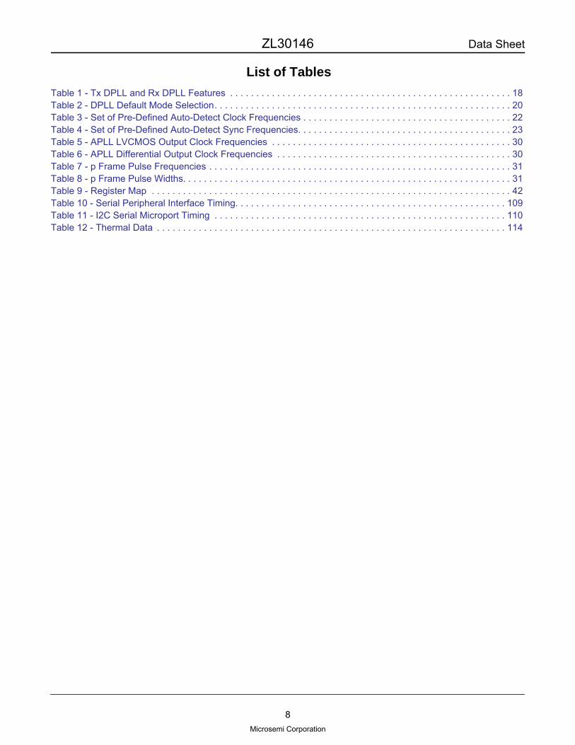
Table 1 - Tx DPLL and Rx DPLL Features . . . . . . . . . . . . . . . . . . . . . . . . . . . . . . . . . . . . . . . . . . . . . . . . . . . . . . 18Table 2 - DPLL Default Mode Selection. . . . . . . . . . . . . . . . . . . . . . . . . . . . . . . . . . . . . . . . . . . . . . . . . . . . . . . . . 20Table 3 - Set of Pre-Defined Auto-Detect Clock Frequencies . . . . . . . . . . . . . . . . . . . . . . . . . . . . . . . . . . . . . . . . 22Table 4 - Set of Pre-Defined Auto-Detect Sync Frequencies. . . . . . . . . . . . . . . . . . . . . . . . . . . . . . . . . . . . . . . . . 23Table 5 - APLL LVCMOS Output Clock Frequencies . . . . . . . . . . . . . . . . . . . . . . . . . . . . . . . . . . . . . . . . . . . . . . 30Table 6 - APLL Differential Output Clock Frequencies . . . . . . . . . . . . . . . . . . . . . . . . . . . . . . . . . . . . . . . . . . . . . 30Table 7 - p Frame Pulse Frequencies . . . . . . . . . . . . . . . . . . . . . . . . . . . . . . . . . . . . . . . . . . . . . . . . . . . . . . . . . . 31Table 8 - p Frame Pulse Widths. . . . . . . . . . . . . . . . . . . . . . . . . . . . . . . . . . . . . . . . . . . . . . . . . . . . . . . . . . . . . . . 31Table 9 - Register Map . . . . . . . . . . . . . . . . . . . . . . . . . . . . . . . . . . . . . . . . . . . . . . . . . . . . . . . . . . . . . . . . . . . . . 42Table 10 - Serial Peripheral Interface Timing. . . . . . . . . . . . . . . . . . . . . . . . . . . . . . . . . . . . . . . . . . . . . . . . . . . . 109Table 11 - I2C Serial Microport Timing . . . . . . . . . . . . . . . . . . . . . . . . . . . . . . . . . . . . . . . . . . . . . . . . . . . . . . . . 110Table 12 - Thermal Data . . . . . . . . . . . . . . . . . . . . . . . . . . . . . . . . . . . . . . . . . . . . . . . . . . . . . . . . . . . . . . . . . . . 114
ZL30146 Data Sheet
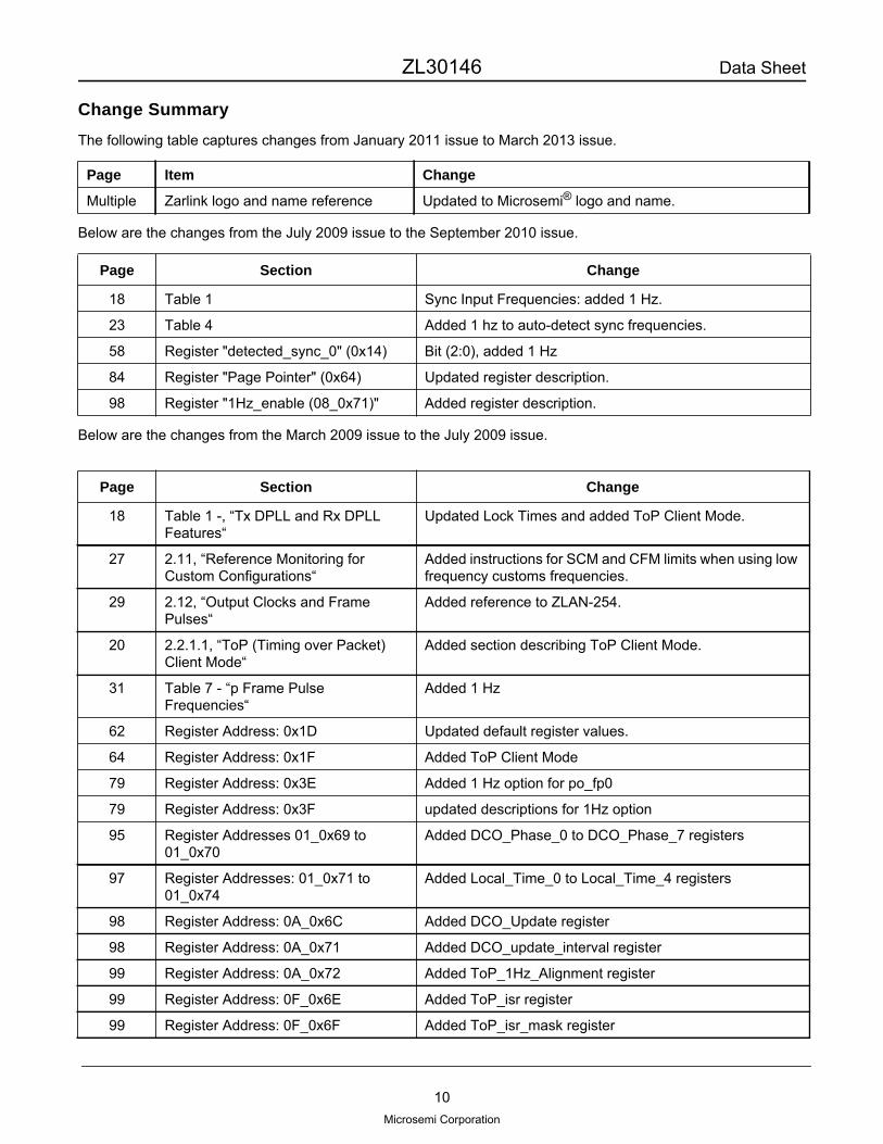
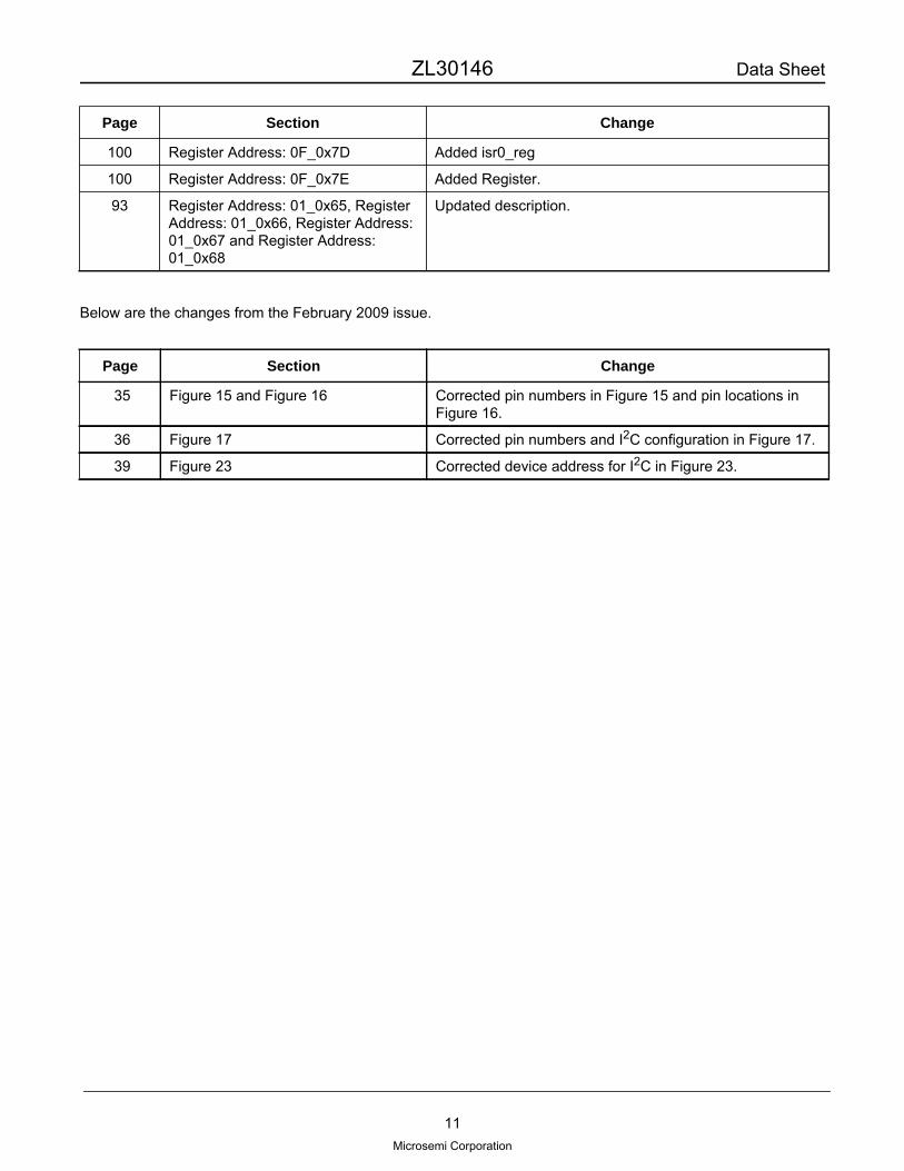
Change SummaryThe following table captures changes from January 2011 issue to March 2013 issue.
Below are the changes from the July 2009 issue to the September 2010 issue.
Below are the changes from the March 2009 issue to the July 2009 issue.
Page Item Change
Multiple Zarlink logo and name reference Updated to Microsemi® logo and name.
Page Section Change
18 Table 1 Sync Input Frequencies: added 1 Hz.
23 Table 4 Added 1 hz to auto-detect sync frequencies.
58 Register "detected_sync_0" (0x14) Bit (2:0), added 1 Hz
84 Register "Page Pointer" (0x64) Updated register description.
98 Register "1Hz_enable (08_0x71)" Added register description.
Page Section Change
18 Table 1 -, “Tx DPLL and Rx DPLL Features“
Updated Lock Times and added ToP Client Mode.
27 2.11, “Reference Monitoring for Custom Configurations“
Added instructions for SCM and CFM limits when using low frequency customs frequencies.
29 2.12, “Output Clocks and Frame Pulses“
Added reference to ZLAN-254.
20 2.2.1.1, “ToP (Timing over Packet) Client Mode“
Added section describing ToP Client Mode.
31 Table 7 - “p Frame Pulse Frequencies“
Added 1 Hz
62 Register Address: 0x1D Updated default register values.
64 Register Address: 0x1F Added ToP Client Mode
79 Register Address: 0x3E Added 1 Hz option for po_fp0
79 Register Address: 0x3F updated descriptions for 1Hz option
95 Register Addresses 01_0x69 to 01_0x70
Added DCO_Phase_0 to DCO_Phase_7 registers
97 Register Addresses: 01_0x71 to 01_0x74
Added Local_Time_0 to Local_Time_4 registers
98 Register Address: 0A_0x6C Added DCO_Update register
98 Register Address: 0A_0x71 Added DCO_update_interval register
99 Register Address: 0A_0x72 Added ToP_1Hz_Alignment register
99 Register Address: 0F_0x6E Added ToP_isr register
99 Register Address: 0F_0x6F Added ToP_isr_mask register
10Microsemi Corporation
ZL30146 Data Sheet
Below are the changes from the February 2009 issue.
100 Register Address: 0F_0x7D Added isr0_reg
100 Register Address: 0F_0x7E Added Register.
93 Register Address: 01_0x65, Register Address: 01_0x66, Register Address: 01_0x67 and Register Address: 01_0x68
Updated description.
Page Section Change
35 Figure 15 and Figure 16 Corrected pin numbers in Figure 15 and pin locations in Figure 16.
36 Figure 17 Corrected pin numbers and I2C configuration in Figure 17.
39 Figure 23 Corrected device address for I2C in Figure 23.
Page Section Change
11Microsemi Corporation
ZL30146 Data Sheet
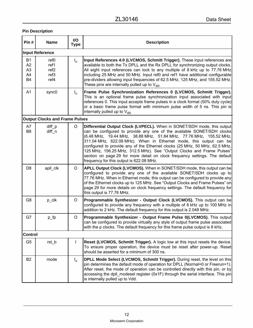
Pin Description
Pin # Name I/OType Description
Input Reference
B1A2A3A4B4
ref0ref1ref2ref3ref4
Iu Input References 4:0 (LVCMOS, Schmitt Trigger). These input references areavailable to both the Tx DPLL and the Rx DPLL for synchronizing output clocks.All eight input references can lock to any multiple of 8 kHz up to 77.76 MHzincluding 25 MHz and 50 MHz. Input ref0 and ref1 have additional configurablepre-dividers allowing input frequencies of 62.5 MHz, 125 MHz, and 155.52 MHz.These pins are internally pulled up to Vdd.
A1 sync0 Iu Frame Pulse Synchronization References 0 (LVCMOS, Schmitt Trigger).This is an optional frame pulse synchronization input associated with inputreferences 0. This input accepts frame pulses in a clock format (50% duty cycle)or a basic frame pulse format with minimum pulse width of 5 ns. This pin isinternally pulled up to Vdd.
Output Clocks and Frame Pulses
A7B8
diff_pdiff_n
O Differential Output Clock (LVPECL). When in SONET/SDH mode, this outputcan be configured to provide any one of the available SONET/SDH clocks(6.48 MHz, 19.44 MHz, 38.88 MHz, 51.84 MHz, 77.76 MHz, 155.52 MHz,311.04 MHz, 622.08 MHz). When in Ethernet mode, this output can beconfigured to provide any of the Ethernet clocks (25 MHz, 50 MHz, 62.5 MHz,125 MHz, 156.25 MHz, 312.5 MHz). See “Output Clocks and Frame Pulses”section on page 29 for more detail on clock frequency settings. The defaultfrequency for this output is 622.08 MHz.
D8 apll_clk O APLL Output Clock (LVCMOS). When in SONET/SDH mode, this output can beconfigured to provide any one of the available SONET/SDH clocks up to77.76 MHz. When in Ethernet mode, this output can be configured to provide anyof the Ethernet clocks up to 125 MHz. See “Output Clocks and Frame Pulses” onpage 29 for more details on clock frequency settings. The default frequency forthis output is 77.76 MHz.
G8 p_clk O Programmable Synthesizer - Output Clock (LVCMOS). This output can beconfigured to provide any frequency with a multiple of 8 kHz up to 100 MHz inaddition to 2 kHz. The default frequency for this output is 2.048 MHz.
G7 p_fp O Programmable Synthesizer - Output Frame Pulse 0(LVCMOS). This outputcan be configured to provide virtually any style of output frame pulse associatedwith the p clocks. The default frequency for this frame pulse output is 8 kHz.
Control
G5 rst_b I Reset (LVCMOS, Schmitt Trigger). A logic low at this input resets the device.To ensure proper operation, the device must be reset after power-up. Resetshould be asserted for a minimum of 300 ns.
B2 mode Iu DPLL Mode Select (LVCMOS, Schmitt Trigger). During reset, the level on thispin determines the default mode of operation for DPLL (Normal=0 or Freerun=1).After reset, the mode of operation can be controlled directly with this pin, or byaccessing the dpll_modesel register (0x1F) through the serial interface. This pinis internally pulled up to Vdd.
12Microsemi Corporation
ZL30146 Data Sheet
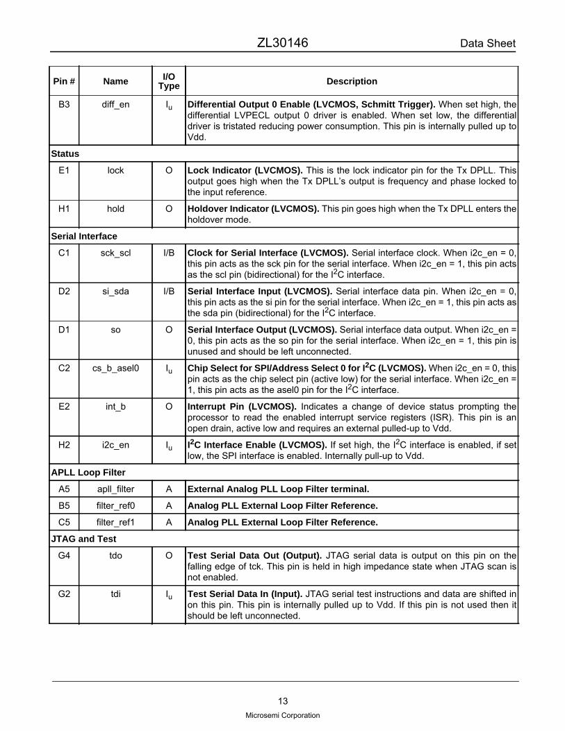
B3 diff_en Iu Differential Output 0 Enable (LVCMOS, Schmitt Trigger). When set high, thedifferential LVPECL output 0 driver is enabled. When set low, the differentialdriver is tristated reducing power consumption. This pin is internally pulled up toVdd.
Status
E1 lock O Lock Indicator (LVCMOS). This is the lock indicator pin for the Tx DPLL. Thisoutput goes high when the Tx DPLL’s output is frequency and phase locked tothe input reference.
H1 hold O Holdover Indicator (LVCMOS). This pin goes high when the Tx DPLL enters theholdover mode.
Serial Interface
C1 sck_scl I/B Clock for Serial Interface (LVCMOS). Serial interface clock. When i2c_en = 0,this pin acts as the sck pin for the serial interface. When i2c_en = 1, this pin actsas the scl pin (bidirectional) for the I2C interface.
D2 si_sda I/B Serial Interface Input (LVCMOS). Serial interface data pin. When i2c_en = 0,this pin acts as the si pin for the serial interface. When i2c_en = 1, this pin acts asthe sda pin (bidirectional) for the I2C interface.
D1 so O Serial Interface Output (LVCMOS). Serial interface data output. When i2c_en =0, this pin acts as the so pin for the serial interface. When i2c_en = 1, this pin isunused and should be left unconnected.
C2 cs_b_asel0 Iu Chip Select for SPI/Address Select 0 for I2C (LVCMOS). When i2c_en = 0, thispin acts as the chip select pin (active low) for the serial interface. When i2c_en =1, this pin acts as the asel0 pin for the I2C interface.
E2 int_b O Interrupt Pin (LVCMOS). Indicates a change of device status prompting theprocessor to read the enabled interrupt service registers (ISR). This pin is anopen drain, active low and requires an external pulled-up to Vdd.
H2 i2c_en Iu I2C Interface Enable (LVCMOS). If set high, the I2C interface is enabled, if setlow, the SPI interface is enabled. Internally pull-up to Vdd.
APLL Loop Filter
A5 apll_filter A External Analog PLL Loop Filter terminal.
B5 filter_ref0 A Analog PLL External Loop Filter Reference.
C5 filter_ref1 A Analog PLL External Loop Filter Reference.
JTAG and Test
G4 tdo O Test Serial Data Out (Output). JTAG serial data is output on this pin on thefalling edge of tck. This pin is held in high impedance state when JTAG scan isnot enabled.
G2 tdi Iu Test Serial Data In (Input). JTAG serial test instructions and data are shifted inon this pin. This pin is internally pulled up to Vdd. If this pin is not used then itshould be left unconnected.
Pin # Name I/OType Description
13Microsemi Corporation
ZL30146 Data Sheet
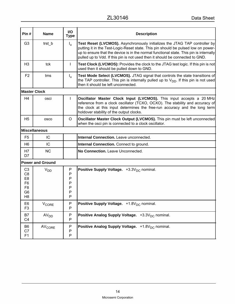
G3 trst_b Iu Test Reset (LVCMOS). Asynchronously initializes the JTAG TAP controller byputting it in the Test-Logic-Reset state. This pin should be pulsed low on power-up to ensure that the device is in the normal functional state. This pin is internallypulled up to Vdd. If this pin is not used then it should be connected to GND.
H3 tck I Test Clock (LVCMOS): Provides the clock to the JTAG test logic. If this pin is notused then it should be pulled down to GND.
F2 tms Iu Test Mode Select (LVCMOS). JTAG signal that controls the state transitions ofthe TAP controller. This pin is internally pulled up to VDD. If this pin is not usedthen it should be left unconnected.
Master Clock
H4 osci I Oscillator Master Clock Input (LVCMOS). This input accepts a 20 MHzreference from a clock oscillator (TCXO, OCXO). The stability and accuracy ofthe clock at this input determines the free-run accuracy and the long termholdover stability of the output clocks.
H5 osco O Oscillator Master Clock Output (LVCMOS). This pin must be left unconnectedwhen the osci pin is connected to a clock oscillator.
Miscellaneous
F5 IC Internal Connection. Leave unconnected.
H6 IC Internal Connection. Connect to ground.
H7D7
NC No Connection. Leave Unconnected.
Power and Ground
C3C8E8F6F8G6H8
VDD PPPPPPP
Positive Supply Voltage. +3.3VDC nominal.
E6F3
VCORE PP
Positive Supply Voltage. +1.8VDC nominal.
B7C4
AVDD PP
Positive Analog Supply Voltage. +3.3VDC nominal.
B6C7F1
AVCORE PPP
Positive Analog Supply Voltage. +1.8VDC nominal.
Pin # Name I/OType Description
14Microsemi Corporation
ZL30146 Data Sheet
I - InputId - Input, Internally pulled downIu - Input, Internally pulled upO - OutputA - AnalogP - PowerG - Ground
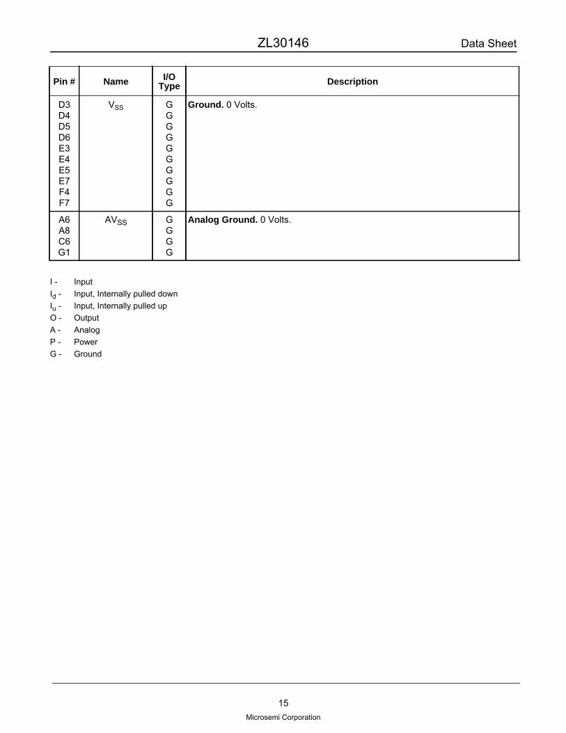
D3D4D5D6E3E4E5E7F4F7
VSS GGGGGGGGGG
Ground. 0 Volts.
A6A8C6G1
AVSS GGGG
Analog Ground. 0 Volts.
Pin # Name I/OType Description
15Microsemi Corporation
ZL30146 Data Sheet
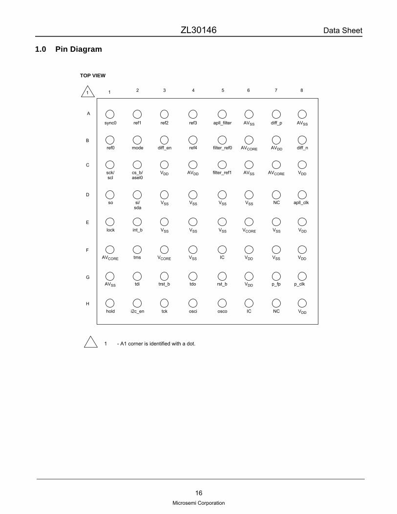
1.0 Pin Diagram
B
C
D
E
F
G
H
2 3 4 5 6 7 81
1 - A1 corner is identified with a dot.
A
sync0
TOP VIEW
ref1 ref2 ref3 apll_filter AVSS diff_p AVSS
ref0 mode diff_en ref4 filter_ref0 AVCORE AVDD diff_n
sck/ cs_b/ VDD AVDD filter_ref1 AVSS AVCORE VDD
so si/ VSS VSS VSS VSS NC apll_clk
lock int_b VSS VSS VSS VCORE VSS VDD
AVCORE tms VCORE VSS IC VDD VSS VDD
AVSS tdi trst_b tdo rst_b VDD p_fp p_clk
hold i2c_en tck osci osco IC NC VDD
1
asel0
sda
scl
16Microsemi Corporation
ZL30146 Data Sheet
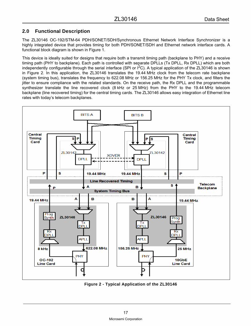
2.0 Functional DescriptionThe ZL30146 OC-192/STM-64 PDH/SONET/SDH/Synchronous Ethernet Network Interface Synchronizer is ahighly integrated device that provides timing for both PDH/SONET/SDH and Ethernet network interface cards. Afunctional block diagram is shown in Figure 1.
This device is ideally suited for designs that require both a transmit timing path (backplane to PHY) and a receivetiming path (PHY to backplane). Each path is controlled with separate DPLLs (Tx DPLL, Rx DPLL) which are bothindependently configurable through the serial interface (SPI or I2C). A typical application of the ZL30146 is shownin Figure 2. In this application, the ZL30146 translates the 19.44 MHz clock from the telecom rate backplane(system timing bus), translates the frequency to 622.08 MHz or 156.25 MHz for the PHY Tx clock, and filters thejitter to ensure compliance with the related standards. On the receive path, the Rx DPLL and the programmablesynthesizer translate the line recovered clock (8 kHz or 25 MHz) from the PHY to the 19.44 MHz telecombackplane (line recovered timing) for the central timing cards. The ZL30146 allows easy integration of Ethernet linerates with today’s telecom backplanes.
Figure 2 - Typical Application of the ZL30146
17Microsemi Corporation
ZL30146 Data Sheet
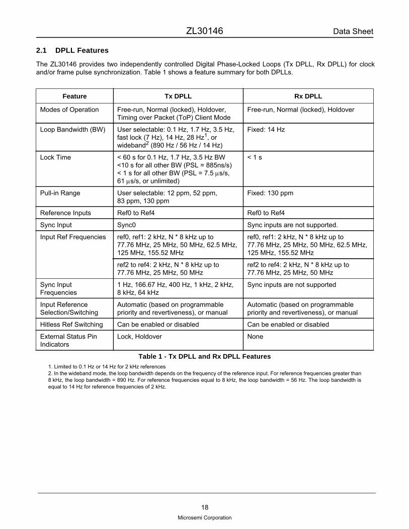
2.1 DPLL Features
The ZL30146 provides two independently controlled Digital Phase-Locked Loops (Tx DPLL, Rx DPLL) for clockand/or frame pulse synchronization. Table 1 shows a feature summary for both DPLLs.
Feature Tx DPLL Rx DPLL
Modes of Operation Free-run, Normal (locked), Holdover, Timing over Packet (ToP) Client Mode
Free-run, Normal (locked), Holdover
Loop Bandwidth (BW) User selectable: 0.1 Hz, 1.7 Hz, 3.5 Hz, fast lock (7 Hz), 14 Hz, 28 Hz1, or wideband2 (890 Hz / 56 Hz / 14 Hz)
1. Limited to 0.1 Hz or 14 Hz for 2 kHz references2. In the wideband mode, the loop bandwidth depends on the frequency of the reference input. For reference frequencies greater than8 kHz, the loop bandwidth = 890 Hz. For reference frequencies equal to 8 kHz, the loop bandwidth = 56 Hz. The loop bandwidth isequal to 14 Hz for reference frequencies of 2 kHz.
Fixed: 14 Hz
Lock Time < 60 s for 0.1 Hz, 1.7 Hz, 3.5 Hz BW<10 s for all other BW (PSL = 885ns/s)< 1 s for all other BW (PSL = 7.5 s/s, 61 s/s, or unlimited)
< 1 s
Pull-in Range User selectable: 12 ppm, 52 ppm, 83 ppm, 130 ppm
Fixed: 130 ppm
Reference Inputs Ref0 to Ref4 Ref0 to Ref4
Sync Input Sync0 Sync inputs are not supported.
Input Ref Frequencies ref0, ref1: 2 kHz, N * 8 kHz up to 77.76 MHz, 25 MHz, 50 MHz, 62.5 MHz, 125 MHz, 155.52 MHz
ref0, ref1: 2 kHz, N * 8 kHz up to 77.76 MHz, 25 MHz, 50 MHz, 62.5 MHz, 125 MHz, 155.52 MHz
ref2 to ref4: 2 kHz, N * 8 kHz up to 77.76 MHz, 25 MHz, 50 MHz
ref2 to ref4: 2 kHz, N * 8 kHz up to 77.76 MHz, 25 MHz, 50 MHz
Sync Input Frequencies
1 Hz, 166.67 Hz, 400 Hz, 1 kHz, 2 kHz, 8 kHz, 64 kHz
Sync inputs are not supported
Input Reference Selection/Switching
Automatic (based on programmable priority and revertiveness), or manual
Automatic (based on programmable priority and revertiveness), or manual
Hitless Ref Switching Can be enabled or disabled Can be enabled or disabled
External Status Pin Indicators
Lock, Holdover None
Table 1 - Tx DPLL and Rx DPLL Features
18Microsemi Corporation
ZL30146 Data Sheet
2.2 DPLL Mode Control
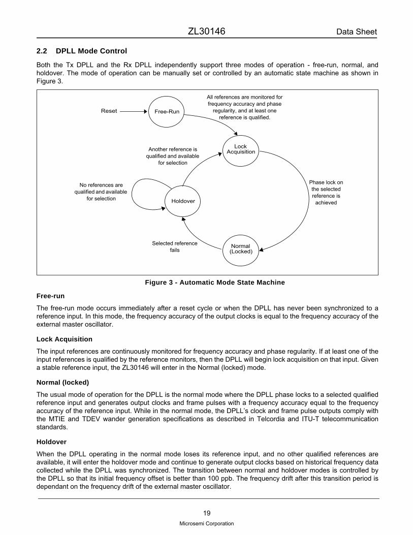
Both the Tx DPLL and the Rx DPLL independently support three modes of operation - free-run, normal, andholdover. The mode of operation can be manually set or controlled by an automatic state machine as shown inFigure 3.
Figure 3 - Automatic Mode State Machine
Free-run
The free-run mode occurs immediately after a reset cycle or when the DPLL has never been synchronized to areference input. In this mode, the frequency accuracy of the output clocks is equal to the frequency accuracy of theexternal master oscillator.
Lock Acquisition
The input references are continuously monitored for frequency accuracy and phase regularity. If at least one of theinput references is qualified by the reference monitors, then the DPLL will begin lock acquisition on that input. Givena stable reference input, the ZL30146 will enter in the Normal (locked) mode.
Normal (locked)
The usual mode of operation for the DPLL is the normal mode where the DPLL phase locks to a selected qualifiedreference input and generates output clocks and frame pulses with a frequency accuracy equal to the frequencyaccuracy of the reference input. While in the normal mode, the DPLL’s clock and frame pulse outputs comply withthe MTIE and TDEV wander generation specifications as described in Telcordia and ITU-T telecommunicationstandards.
Holdover
When the DPLL operating in the normal mode loses its reference input, and no other qualified references areavailable, it will enter the holdover mode and continue to generate output clocks based on historical frequency datacollected while the DPLL was synchronized. The transition between normal and holdover modes is controlled bythe DPLL so that its initial frequency offset is better than 100 ppb. The frequency drift after this transition period isdependant on the frequency drift of the external master oscillator.
Reset
Another reference is qualified and available
for selection
Phase lock on the selected reference is
achieved
LockAcquisition
Normal(Locked)
No references are qualified and available
for selection
Free-Run
Holdover
Selected reference fails
All references are monitored for frequency accuracy and phase
regularity, and at least one reference is qualified.
Normal(Locked)
19Microsemi Corporation
ZL30146 Data Sheet
2.2.1 Tx DPLL Mode Of Operation
During reset, the level on the mode pin determines the default start-up mode of operation for DPLL. Table 2 showsthe settings for this pin. When left unconnected, the default mode of operation will be set to manual freerun mode.The selected value is reflected in the dpll_modesel register (0x1F).
After reset, the mode of operation can be controlled by software using the dpll_modesel register (0x1F), or it can becontrolled using the mode pin by setting the dpll_mode_hsw bit of the use_hw_ctrl register (0x01) to 1.
2.2.1.1 ToP (Timing over Packet) Client Mode
In software control mode the ZL30146 can also be set in Timing over Packet (ToP) Client Mode using thedpll1_modesel register (0x1F).
ToP Client mode allows external software to control DCO frequency offset of Tx_DPLL using the 28 bit 2'scomplement value in the DCO_freq_offset registers (page 1, addresses 0x65 to 0x68). The offset is programmed insteps according to the following equation.
LSB = 2-40 * (80MHz/65,536MHz) *109ppb
In ToP client mode, the ZL30146 also samples the DCO Phase Word and Local System time to be read by the ToPclock recovery algorithm software.
The 64 bit DCO phase Word is available in the DCO_Phase registers (page 1, address 0x69 to 0x70). The 32 bitLocal System Time is available in the Local Time registers (page 1, address 0x71 to 0x74)
For more details contact your local Microsemi FAE.
2.2.2 Rx DPLL Mode of Operation
The mode of operation for the Rx DPLL can only be controlled in software using the rx_dpll_modesel register(0x2C). By default, its mode of operation is set to Free Run.
2.3 Loop Bandwidth
The loop bandwidth determines the amount of jitter or wander filtering that is provided by the DPLL. The loopbandwidth for the Tx DPLL is programmable using the bandwidth field of the tx_dpll_control_register_0 register(0x1D). Options are 0.1 Hz, 1.7 Hz, 3.5 Hz, fast lock (7 Hz), 14 Hz, 28 Hz, and 890 Hz. The Rx DPLL loopbandwidth is not programmable and is fixed at 14 Hz.
mode Function
0 Set the default mode of operation to Manual Normal Mode. In this mode, automatic reference switching is disabled and the selected reference is determined by the dpll_refsel register (0x20). If the selected reference fails, the device automatically enters the holdover mode.
1 Set the default state to Manual Freerun Mode. In this mode, automatic reference switching is disabled and the DPLL stays in the free-run mode.
Table 2 - DPLL Default Mode Selection
20Microsemi Corporation
ZL30146 Data Sheet
2.4 Pull-in/hold-in Range
The pull-in range defines the maximum input frequency range that the DPLL can lock to. The pull-in range forDPLL1 is programmable using the dpll1_pull_in_range register (0x29). The hold-in range, which defines the rangeof input frequencies that the PLL will continue to lock to, is equal to the pull-in range. The pull-in/hold-in range forDPLL2 is fixed at +/-130 ppm.
2.5 Hitless Reference Switching
With hitless reference switching enabled, the phase difference between the originally selected reference and thenewly selected reference is absorbed by the DPLL preventing a possible non-compliant phase transient at itsoutput. The hs_en bit of the tx/rx_dpll_ctrl_0 registers (0x1D, 0x2A) allows this feature to be enabled or disabled.When disabled, the DPLL will align its output to the new reference at a rate of alignment which is dependant on thephase slope limit set in the dpll_ph_slopelim field of the dpll_ctrl_0 register (0x1D).
2.6 Free-run Frequency Offset
When operating in Free Run mode, the accuracy of the output clocks is equal to that of the oscillator connected tothe Master Clock Input (OSCi). The ZL30146 allows the user to offset this frequency by +/-149ppm by using the 28bit 2's complement value in the DCO_freq_offset registers (page 1, addresses 0x65, 0x66, 0x67, and 0x68). Theoffset is programmed in steps according to the following equation.
LSB = 2-40 * (80MHz/65,536MHz) *109ppb
The offset can be enabled or disabled independently for each of the two DPLLs. To enable the free run frequencyoffset for Tx DPLL set the freq_offset_en bit of the tx_dpll_ctrl_1 register (page 0, address 0x1E, bit 1). To enablethe free run frequency offset for Rx DPLL set the freq_offset_en bit of the rx_dpll_ctrl_1 register (page 0, address0x2B, bit 1).
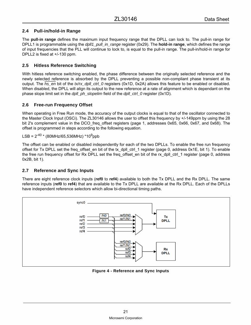
2.7 Reference and Sync Inputs
There are eight reference clock inputs (ref0 to ref4) available to both the Tx DPLL and the Rx DPLL. The samereference inputs (ref0 to ref4) that are available to the Tx DPLL are available at the Rx DPLL. Each of the DPLLshave independent reference selectors which allow bi-directional timing paths.
Figure 4 - Reference and Sync Inputs
21Microsemi Corporation
ZL30146 Data Sheet
Each of the reference inputs (ref0 to ref4) accept a single-ended LVCMOS clock with a frequency ranging from2 kHz to 77.76 MHz. The first two reference inputs (ref0 and ref1) have programmable pre-dividers (N1, N2) whichallows them to lock to frequencies higher than 77.76 MHz or to non-standard frequencies. By default the pre-dividers divide by 1, but they can be programmed to divide by 1.5, 2, 2.5, 3, 4, 5, 6, 7, and 8 using the ref0_div andref1_div bits of the predivider_control register (0x7E). For example, an input frequency of 125 MHz can be divideddown by 5 using the pre-dividers to create a 25 MHz input reference. The resulting 25 MHz can then beprogrammed as a custom input frequency. Similarly, a 62.5 MHz input clock can be divided by 2.5 to create25 MHz. Note that division by non-integer values (e.g., 1.5, 2.5) is achieved by using both the rising andfalling edges of the input reference. This may cause higher jitter levels at the output clocks when thereference input does not have a 50% duty cycle.
Built-in frequency detection circuitry automatically determines the frequency of the reference if its frequency iswithin the set of pre-defined frequencies as shown in Table 3. Once detected, the resulting frequency of thereference can be read from the ref_frq_detected registers (0x10 - 0x11).
Two additional custom reference frequencies (Custom A and Custom B) are also programmable using thecustA_mult and custB_mult registers (0x67, 0x68, 0x71, 0x72). These custom frequencies are programmable as8 kHz * N up to 77.76 MHz (where N = 1 to 9720), or 2 kHz (when N = 0). The ref_freq_mode_0 register (0x65) areused to configure each of the reference inputs as auto-detect, custom A, or custom B.
2 kHz 8.192 MHz
8 kHz 16.384 MHz
64 kHz 19.44 MHz
1.544 MHz 38.88 MHz
2.048 MHz 77.76 MHz
6.48 MHz
Table 3 - Set of Pre-Defined Auto-Detect Clock Frequencies
22Microsemi Corporation
ZL30146 Data Sheet
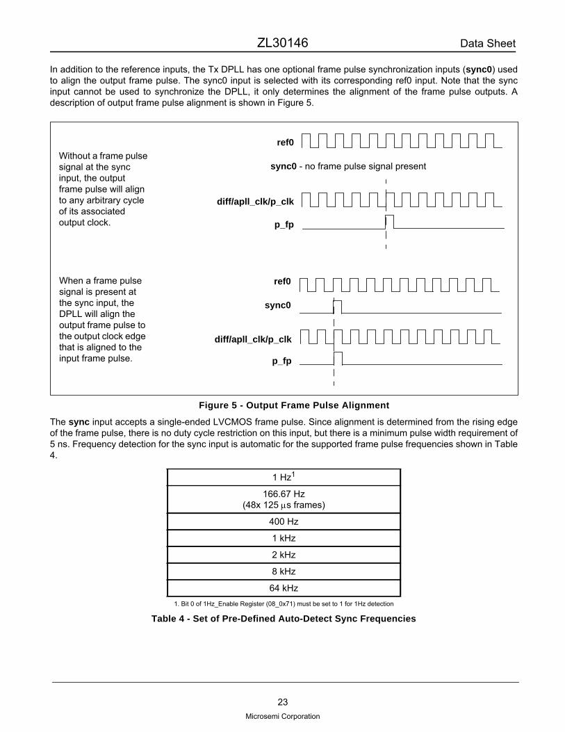
In addition to the reference inputs, the Tx DPLL has one optional frame pulse synchronization inputs (sync0) usedto align the output frame pulse. The sync0 input is selected with its corresponding ref0 input. Note that the syncinput cannot be used to synchronize the DPLL, it only determines the alignment of the frame pulse outputs. Adescription of output frame pulse alignment is shown in Figure 5.
Figure 5 - Output Frame Pulse Alignment
The sync input accepts a single-ended LVCMOS frame pulse. Since alignment is determined from the rising edgeof the frame pulse, there is no duty cycle restriction on this input, but there is a minimum pulse width requirement of5 ns. Frequency detection for the sync input is automatic for the supported frame pulse frequencies shown in Table4.
1 Hz1
166.67 Hz (48x 125 s frames)
400 Hz
1 kHz
2 kHz
8 kHz
64 kHz1. Bit 0 of 1Hz_Enable Register (08_0x71) must be set to 1 for 1Hz detection
Table 4 - Set of Pre-Defined Auto-Detect Sync Frequencies
ref0
diff/apll_clk/p_clk
p_fp
Without a frame pulse signal at the sync input, the output frame pulse will align to any arbitrary cycle of its associated output clock.
sync0 - no frame pulse signal present
When a frame pulse signal is present at the sync input, the DPLL will align the output frame pulse to the output clock edge that is aligned to the input frame pulse.
ref0
sync0
diff/apll_clk/p_clk
p_fp
23Microsemi Corporation
ZL30146 Data Sheet
2.8 Reference Input Selection
Both the Tx DPLL and the Rx DPLL can independently select any of the qualified input references forsynchronization. Reference selection can be automatic or manual depending on the dplln_modesel registers (0x1F,0x2C). For automatic reference selection, the mode selection register must be set to the "Automatic Normal Mode”setting. For manual reference selection, set the mode selection registers to the "Manual Normal Mode".
In the case of automatic reference selection, the selection criteria is based on reference qualification, input priority,and the revertive setting. Only references that are valid can be selected by the automatic state machine. If there areno valid references available, then the DPLL will automatically enter the holdover mode. Each of the references hasan assignable priority using tx_dpll_ref_pri_ctrl registers (0x24 to 0x27), and the input priority for the Rx DPLL isdefined in the rx_dpll_ref_pri_ctrl registers (0x30 to 0x34). Any of the references can be prevented from beingselected by setting their priority to "1111".
The revert_en bit of the dplln_control_register_1 registers (0x1E, 0x2B) controls the revertive switching option forthe DPLLs. With revertive switching enabled, the highest priority reference input with a valid reference is alwaysselected. If a reference with a higher priority becomes valid, then a reference switchover to that reference will beinitiated. With non-revertive switching, the active reference will always remain selected while it is valid. If thisreference becomes invalid, a reference switchover to a valid reference with the highest priority will be initiated. Notethat if two or more references have been assigned the same priority, then priority will be given to the lowestreference number (e.g., if ref2 and ref4 have the same assigned priority, then ref2 will have higher priority overref4).
The revertive feature can also be applied to individual references using the dplln_reference_revertive_controlregisters (0x23, 0x30).
When the dpll_modesel register is set to the "Manual Normal Mode", the active reference is selected using thetx_dpll_refsel or the rx_dpll_refsel registers (0x20, 0x2D). If the defined reference is not valid, then the DPLL willautomatically enter the holdover mode.
2.9 Reference Monitoring
All input references (ref0 to ref4) are monitored for frequency accuracy and phase regularity. New references arequalified before they can be selected as a synchronization source, and qualified references are continuouslymonitored to ensure that they are suitable for synchronization. The process of qualifying a reference depends onfour levels of monitoring.
Single Cycle Monitor (SCM)The SCM block measures the period of each reference clock cycle to detect phase irregularities or a missing clockedge. In general, if the measured period deviates by more than 50% from the nominal period, then an SCM failure(scm_fail) is declared.
Coarse Frequency Monitor (CFM)The CFM block monitors the reference frequency over a measurement period of 30 s so that it can quickly detectlarge changes in frequency. A CFM failure (cfm_fail) is triggered when the frequency has changed by more than 3%or approximately 30000 ppm.
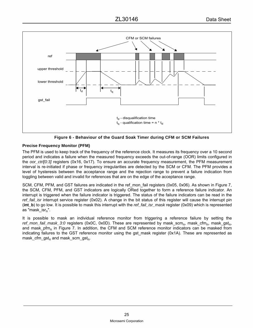
Guard Soak Timer (GST)The SCM and the CFM are used to quickly detect failures of the reference clocks. To prevent intermittent failuresfrom triggering a false reference failure, the SCM and the CFM failure indicators are processed by the Guard SoakTimer. The GST block mimics the operation of an analog integrator by accumulating failure events from the CFMand the SCM blocks and applying a selectable rate of decay when no failures are detected. A GST failure (gst_fail)is triggered when the accumulated failures have reached the upper threshold during the disqualification observationwindow. When there are no CFM or SCM failures, the accumulator decrements until it reaches its lower thresholdduring the qualification window.
24Microsemi Corporation
ZL30146 Data Sheet
Figure 6 - Behaviour of the Guard Soak Timer during CFM or SCM Failures
Precise Frequency Monitor (PFM)The PFM is used to keep track of the frequency of the reference clock. It measures its frequency over a 10 secondperiod and indicates a failure when the measured frequency exceeds the out-of-range (OOR) limits configured inthe oor_ctrl[0:3] registers (0x16, 0x17). To ensure an accurate frequency measurement, the PFM measurementinterval is re-initiated if phase or frequency irregularities are detected by the SCM or CFM. The PFM provides alevel of hysteresis between the acceptance range and the rejection range to prevent a failure indication fromtoggling between valid and invalid for references that are on the edge of the acceptance range.
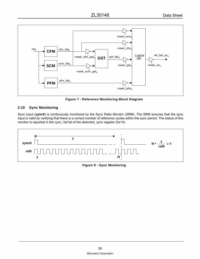
SCM, CFM, PFM, and GST failures are indicated in the ref_mon_fail registers (0x05, 0x06). As shown in Figure 7,the SCM, CFM, PFM, and GST indicators are logically ORed together to form a reference failure indicator. Aninterrupt is triggered when the failure indicator is triggered. The status of the failure indicators can be read in theref_fail_isr interrupt service register (0x02). A change in the bit status of this register will cause the interrupt pin(int_b) to go low. It is possible to mask this interrupt with the ref_fail_isr_mask register (0x09) which is representedas "mask_isrn".
It is possible to mask an individual reference monitor from triggering a reference failure by setting theref_mon_fail_mask_3:0 registers (0x0C, 0x0D). These are represented by mask_scmn, mask_cfmn, mask_gstn,and mask_pfmn in Figure 7. In addition, the CFM and SCM reference monitor indicators can be masked fromindicating failures to the GST reference monitor using the gst_mask register (0x1A). These are represented asmask_cfm_gstn and mask_scm_gstn.
ref
CFM or SCM failures
upper threshold
lower threshold
td - disqualification timetq - qualification time = n * td
td tq
gst_fail
25Microsemi Corporation
ZL30146 Data Sheet
Figure 7 - Reference Monitoring Block Diagram
2.10 Sync Monitoring
Sync input (sync0) is continuously monitored by the Sync Ratio Monitor (SRM). The SRM ensures that the syncinput is valid by verifying that there is a correct number of reference cycles within the sync period. The status of thismonitor is reported in the sync_fail bit of the detected_sync register (0x14).
Figure 8 - Sync Monitoring
pfm_failn
cfm_failn
scm_failn
gst_failn
refn CFMGST
SCM
PFM
mask_cfm_gstn
mask_scm_gstn
mask_pfmn
mask_gstn
mask_cfmn
mask_scmn
LogicalOR
ref_fail_isrn
mask_isrn
ref0
sync0T
N * 1ref0
= T
1 N
26Microsemi Corporation
ZL30146 Data Sheet
2.11 Reference Monitoring for Custom Configurations
As described in Section 2.7, “Reference and Sync Inputs“, two additional custom reference input frequencies(Custom A, Custom B) are definable allowing a reference input to accept any multiple of 8 kHz up to 77.76 MHz.
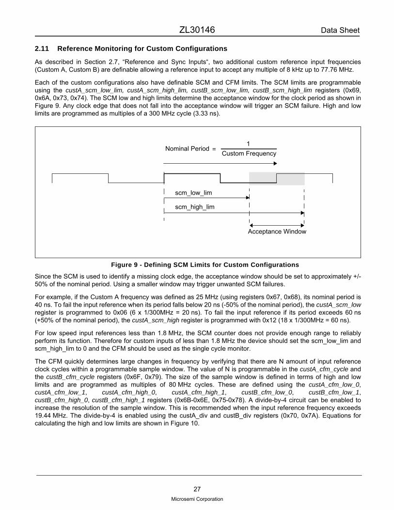
Each of the custom configurations also have definable SCM and CFM limits. The SCM limits are programmableusing the custA_scm_low_lim, custA_scm_high_lim, custB_scm_low_lim, custB_scm_high_lim registers (0x69,0x6A, 0x73, 0x74). The SCM low and high limits determine the acceptance window for the clock period as shown inFigure 9. Any clock edge that does not fall into the acceptance window will trigger an SCM failure. High and lowlimits are programmed as multiples of a 300 MHz cycle (3.33 ns).
Figure 9 - Defining SCM Limits for Custom Configurations
Since the SCM is used to identify a missing clock edge, the acceptance window should be set to approximately +/-50% of the nominal period. Using a smaller window may trigger unwanted SCM failures.
For example, if the Custom A frequency was defined as 25 MHz (using registers 0x67, 0x68), its nominal period is40 ns. To fail the input reference when its period falls below 20 ns (-50% of the nominal period), the custA_scm_lowregister is programmed to 0x06 (6 x 1/300MHz = 20 ns). To fail the input reference if its period exceeds 60 ns(+50% of the nominal period), the custA_scm_high register is programmed with 0x12 (18 x 1/300MHz = 60 ns).
For low speed input references less than 1.8 MHz, the SCM counter does not provide enough range to reliablyperform its function. Therefore for custom inputs of less than 1.8 MHz the device should set the scm_low_lim andscm_high_lim to 0 and the CFM should be used as the single cycle monitor.
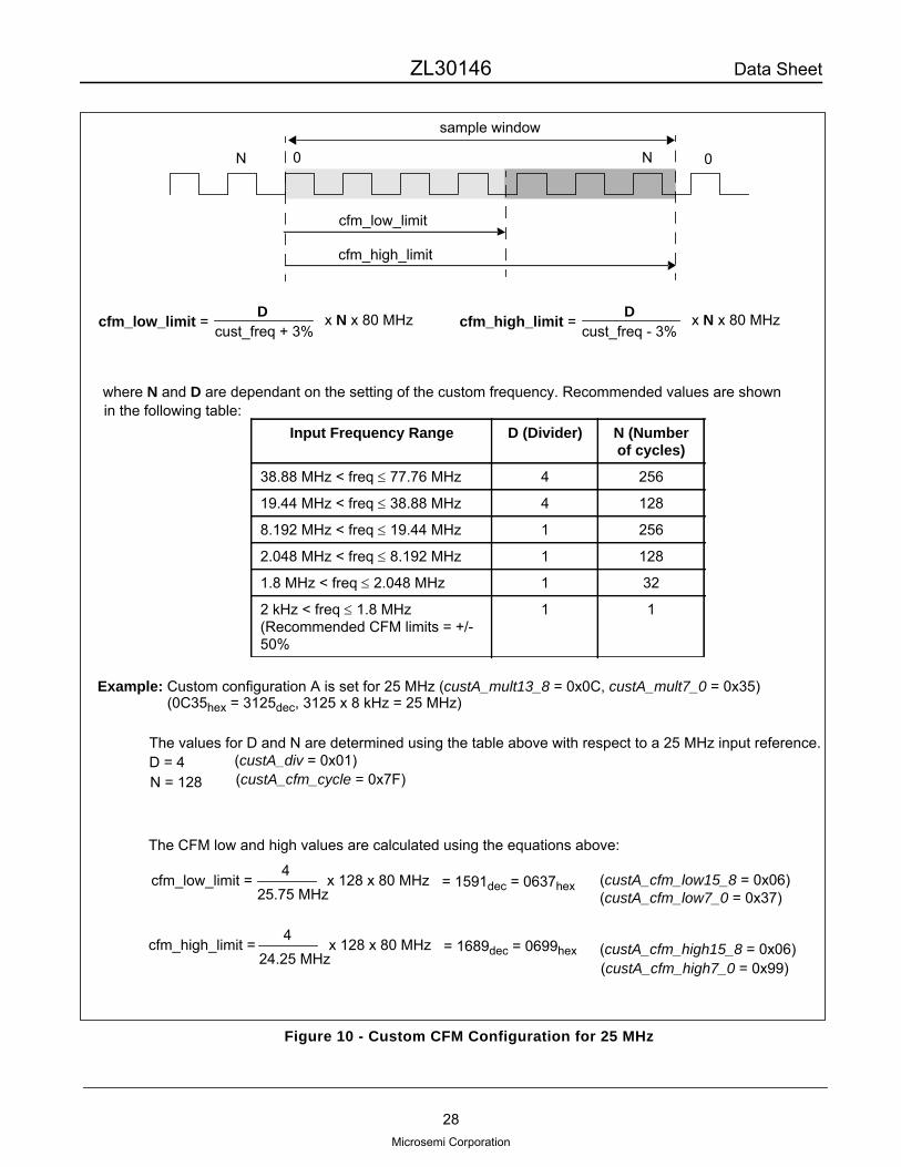
The CFM quickly determines large changes in frequency by verifying that there are N amount of input referenceclock cycles within a programmable sample window. The value of N is programmable in the custA_cfm_cycle andthe custB_cfm_cycle registers (0x6F, 0x79). The size of the sample window is defined in terms of high and lowlimits and are programmed as multiples of 80 MHz cycles. These are defined using the custA_cfm_low_0,custA_cfm_low_1, custA_cfm_high_0, custA_cfm_high_1, custB_cfm_low_0, custB_cfm_low_1,custB_cfm_high_0, custB_cfm_high_1 registers (0x6B-0x6E, 0x75-0x78). A divide-by-4 circuit can be enabled toincrease the resolution of the sample window. This is recommended when the input reference frequency exceeds19.44 MHz. The divide-by-4 is enabled using the custA_div and custB_div registers (0x70, 0x7A). Equations forcalculating the high and low limits are shown in Figure 10.
Nominal Period
scm_low_lim
scm_high_lim
= 1
Custom Frequency
Acceptance Window
27Microsemi Corporation
ZL30146 Data Sheet
Figure 10 - Custom CFM Configuration for 25 MHz
cfm_low_limit
cfm_high_limit
sample window
0 N 0N
Input Frequency Range D (Divider) N (Number of cycles)
38.88 MHz < freq 77.76 MHz 4 256
19.44 MHz < freq 38.88 MHz 4 128
8.192 MHz < freq 19.44 MHz 1 256
2.048 MHz < freq 8.192 MHz 1 128
1.8 MHz < freq 2.048 MHz 1 32
2 kHz < freq 1.8 MHz (Recommended CFM limits = +/-50%
1 1
cfm_low_limit = D
cust_freq + 3%x N x 80 MHz cfm_high_limit =
Dcust_freq - 3%
x N x 80 MHz
where N and D are dependant on the setting of the custom frequency. Recommended values are shown in the following table:
cfm_low_limit = 4
25.75 MHzx 128 x 80 MHz = 1591dec = 0637hex
cfm_high_limit = 4
24.25 MHzx 128 x 80 MHz = 1689dec = 0699hex
(custA_cfm_low15_8 = 0x06)(custA_cfm_low7_0 = 0x37)
(custA_cfm_high7_0 = 0x99)(custA_cfm_high15_8 = 0x06)
(custA_cfm_cycle = 0x7F)(custA_div = 0x01)
Example: Custom configuration A is set for 25 MHz (custA_mult13_8 = 0x0C, custA_mult7_0 = 0x35)
The values for D and N are determined using the table above with respect to a 25 MHz input reference. D = 4 N = 128
The CFM low and high values are calculated using the equations above:
(0C35hex = 3125dec, 3125 x 8 kHz = 25 MHz)
28Microsemi Corporation
ZL30146 Data Sheet
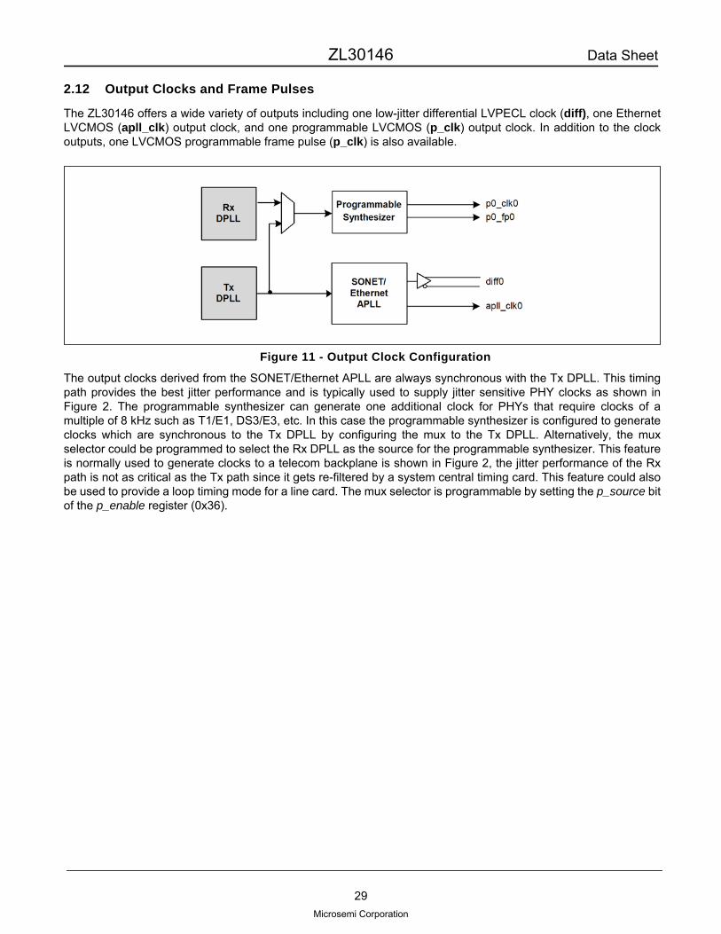
2.12 Output Clocks and Frame Pulses
The ZL30146 offers a wide variety of outputs including one low-jitter differential LVPECL clock (diff), one EthernetLVCMOS (apll_clk) output clock, and one programmable LVCMOS (p_clk) output clock. In addition to the clockoutputs, one LVCMOS programmable frame pulse (p_clk) is also available.
Figure 11 - Output Clock Configuration
The output clocks derived from the SONET/Ethernet APLL are always synchronous with the Tx DPLL. This timingpath provides the best jitter performance and is typically used to supply jitter sensitive PHY clocks as shown inFigure 2. The programmable synthesizer can generate one additional clock for PHYs that require clocks of amultiple of 8 kHz such as T1/E1, DS3/E3, etc. In this case the programmable synthesizer is configured to generateclocks which are synchronous to the Tx DPLL by configuring the mux to the Tx DPLL. Alternatively, the muxselector could be programmed to select the Rx DPLL as the source for the programmable synthesizer. This featureis normally used to generate clocks to a telecom backplane is shown in Figure 2, the jitter performance of the Rxpath is not as critical as the Tx path since it gets re-filtered by a system central timing card. This feature could alsobe used to provide a loop timing mode for a line card. The mux selector is programmable by setting the p_source bitof the p_enable register (0x36).
29Microsemi Corporation
ZL30146 Data Sheet
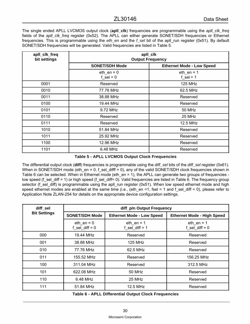
The single ended APLL LVCMOS output clock (apll_clk) frequencies are programmable using the apll_clk_freqfields of the apll_clk_freq register (0x52). The APLL can either generate SONET/SDH frequencies or Ethernetfrequencies. This is programmable using the eth_en and the f_sel bit of the apll_run register (0x51). By defaultSONET/SDH frequencies will be generated. Valid frequencies are listed in Table 5.
The differential output clock (diff) frequencies is programmable using the diff_sel bits of the diff_sel register (0x61).When in SONET/SDH mode (eth_en = 0, f_sel_difff = 0), any of the valid SONET/SDH clock frequencies shown inTable 6 can be selected. When in Ethernet mode (eth_en = 1), the APLL can generate two groups of frequencies -low speed (f_sel_diff = 1) or high speed (f_sel_diff= 0). Valid frequencies are listed in Table 6. The frequency groupselector (f_sel_diff) is programmable using the apll_run register (0x51). When low speed ethernet mode and highspeed ethernet modes are enabled at the same time (i.e., (eth_en =1, fsel = 1 and f_sel_diff = 0), please refer toApplication Note ZLAN-254 for details on the appropriate device configuration settings.
apll_clk_freqbit settings
apll_clk Output Frequency
SONET/SDH Mode Ethernet Mode - Low Speedeth_en = 0f_sel = 0
eth_en = 1f_sel = 1
0001 Reserved 125 MHz0010 77.76 MHz 62.5 MHz0011 38.88 MHz Reserved0100 19.44 MHz Reserved0101 9.72 MHz 50 MHz0110 Reserved 25 MHz0111 Reserved 12.5 MHz1010 51.84 MHz Reserved1011 25.92 MHz Reserved1100 12.96 MHz Reserved1101 6.48 MHz Reserved
Table 5 - APLL LVCMOS Output Clock Frequencies
diff_sel Bit Settings
diff_p/n Output Frequency
SONET/SDH Mode Ethernet Mode - Low Speed Ethernet Mode - High Speed
eth_en = 0f_sel_diff = 0
eth_en = 1f_sel_diff = 1
eth_en = 1f_sel_diff = 0
000 19.44 MHz Reserved Reserved
001 38.88 MHz 125 MHz Reserved
010 77.76 MHz 62.5 MHz Reserved
011 155.52 MHz Reserved 156.25 MHz
100 311.04 MHz Reserved 312.5 MHz
101 622.08 MHz 50 MHz Reserved
110 6.48 MHz 25 MHz Reserved
111 51.84 MHz 12.5 MHz Reserved
Table 6 - APLL Differential Output Clock Frequencies
30Microsemi Corporation
ZL30146 Data Sheet
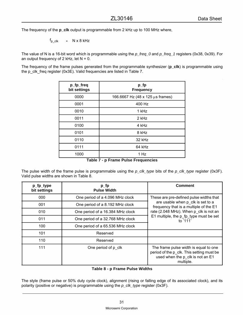
The frequency of the p_clk output is programmable from 2 kHz up to 100 MHz where,
The value of N is a 16-bit word which is programmable using the p_freq_0 and p_freq_1 registers (0x38, 0x39). Foran output frequency of 2 kHz, let N = 0.
The frequency of the frame pulses generated from the programmable synthesizer (p_clk) is programmable usingthe p_clk_freq register (0x3E). Valid frequencies are listed in Table 7.
.
Table 7 - p Frame Pulse Frequencies
The pulse width of the frame pulse is programmable using the p_clk_type bits of the p_clk_type register (0x3F).Valid pulse widths are shown in Table 8.
The style (frame pulse or 50% duty cycle clock), alignment (rising or falling edge of its associated clock), and itspolarity (positive or negative) is programmable using the p_clk_type register (0x3F).
p_fp_freqbit settings
p_fp Frequency
0000 166.6667 Hz (48 x 125 s frames)
0001 400 Hz
0010 1 kHz
0011 2 kHz
0100 4 kHz
0101 8 kHz
0110 32 kHz
0111 64 kHz
1000 1 Hz
p_fp_typebit settings
p_fp Pulse Width
Comment
000 One period of a 4.096 MHz clock These are pre-defined pulse widths that are usable when p_clk is set to a
frequency that is a multiple of the E1 rate (2.048 MHz). When p_clk is not an E1 multiple, the p_fp_type must be set
to ’111’
001 One period of a 8.192 MHz clock
010 One period of a 16.384 MHz clock
011 One period of a 32.768 MHz clock
100 One period of a 65.536 MHz clock
101 Reserved
110 Reserved
111 One period of p_clk The frame pulse width is equal to one period of the p_clk. This setting must be
used when the p_clk is not an E1 multiple.
Table 8 - p Frame Pulse Widths
fp_clk = N x 8 kHz
31Microsemi Corporation
ZL30146 Data Sheet
2.12.1 Output Clock and Frame Pulse Squelching
A clock squelching feature is available which allows forcing an output clock to a specific logic level. Theapll_clk_run and the bits of the enet_run_register (0x51) control the single ended output. The programmable clockoutputs can also be forced to a logic low level using the p_clk_run bits of the p_run register (0x37).
2.12.2 Disabling Output Clocks and Frame Pulses
Unused outputs can be set to a high impedance state to reduce power consumption. The differential output can bedisabled using the diff_en bits of the diff_ctrl register (0x60). The single ended output can be disabled using theapll_clk_en bits of the enet_enable register (0x50). The programmable clock can be disabled using the p_clk_enbits of the p_enable register (0x36).
When not in use, the frame pulse output can be disabled using the p_clk_en bits of the p_enable register (0x36).
2.12.3 Disabling Output Synthesizers
In applications where none of the Ethernet APLL clocks are used, the entire APLL can be disabled to conservepower using the enet_en bit of the enet_enable register (0x50). The programmable synthesizer can also bedisabled by using the p_en bit of the p_enable register (0x36).
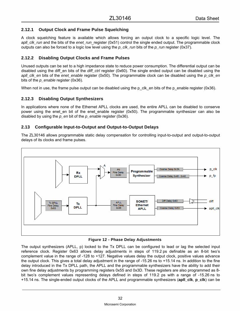
2.13 Configurable Input-to-Output and Output-to-Output Delays
The ZL30146 allows programmable static delay compensation for controlling input-to-output and output-to-outputdelays of its clocks and frame pulses.
Figure 12 - Phase Delay Adjustments
The output synthesizers (APLL, p) locked to the Tx DPLL can be configured to lead or lag the selected inputreference clock. Register 0x63 allows delay adjustments in steps of 119.2 ps definable as an 8-bit two’scomplement value in the range of -128 to +127. Negative values delay the output clock, positive values advancethe output clock. This gives a total delay adjustment in the range of -15.26 ns to +15.14 ns. In addition to the finedelay introduced in the Tx DPLL path, the APLL and the programmable synthesizers have the ability to add theirown fine delay adjustments by programming registers 0x55 and 0x3D. These registers are also programmed as 8-bit two’s complement values representing delays defined in steps of 119.2 ps with a range of -15.26 ns to+15.14 ns. The single-ended output clocks of the APLL and programmable synthesizers (apll_clk, p_clk) can be
32Microsemi Corporation
ZL30146 Data Sheet
independently offset by 90, 180 and 270 degrees using the coarse delay registers (0x53, 0x3A). The APLLdifferential output (diff) can be independently delayed by -1.6 ns, 0 ns, +1.6 ns, or +3.2 ns. This delay isprogrammable using the diff_adjust bits of the diff_ctrl register (0x60). The output frame pulses (p_clk) can beindependently offset with respect to each other using the frame pulse delay registers (0x40 - 0x42). Frame pulsegenerated from the programmable synthesizer (p_clk) that is associated with p clock (p_clk) that are multiples of2.048 MHz (E1) can be delayed in steps of 1/262.144 MHz (or approx. 3.81 ns). The delay value is programmed asa 16-bit value defined in registers 0x40/0x41 for p_clk. The maximum amount of delay is 125 s (= 32767 *1/262.14 MHz). In addition, the frame pulse can be delayed in steps of 125 s (up to 2^6 * 125 s = 8 ms) using the0x42 register for p_clk.
2.14 Master Clock Interface
The master oscillator determines the DPLL’s free-run frequency accuracy and holdover stability. The referencemonitor circuitry also uses this frequency as its point of reference (0 ppm) when making frequency measurements.The master clock interface was designed to accept either a free-running clock oscillator (XO) or a crystal (XTAL).Refer to application note ZLAN-68 for a list of recommended clock oscillators.
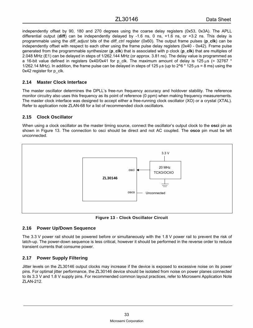
2.15 Clock Oscillator
When using a clock oscillator as the master timing source, connect the oscillator’s output clock to the osci pin asshown in Figure 13. The connection to osci should be direct and not AC coupled. The osco pin must be leftunconnected.
Figure 13 - Clock Oscillator Circuit
2.16 Power Up/Down Sequence
The 3.3 V power rail should be powered before or simultaneously with the 1.8 V power rail to prevent the risk oflatch-up. The power-down sequence is less critical, however it should be performed in the reverse order to reducetransient currents that consume power.
2.17 Power Supply Filtering
Jitter levels on the ZL30146 output clocks may increase if the device is exposed to excessive noise on its powerpins. For optimal jitter performance, the ZL30146 device should be isolated from noise on power planes connectedto its 3.3 V and 1.8 V supply pins. For recommended common layout practices, refer to Microsemi Application NoteZLAN-212.
osci
3.3 V
20 MHz
osco Unconnected
ZL30146TCXO/OCXO
33Microsemi Corporation
ZL30146 Data Sheet
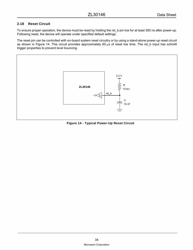
2.18 Reset Circuit
To ensure proper operation, the device must be reset by holding the rst_b pin low for at least 300 ns after power-up.Following reset, the device will operate under specified default settings.
The reset pin can be controlled with on-board system reset circuitry or by using a stand-alone power-up reset circuitas shown in Figure 14. This circuit provides approximately 60 s of reset low time. The rst_b input has schmitttrigger properties to prevent level bouncing.
Figure 14 - Typical Power-Up Reset Circuit
ZL30146 R
C
3.3 V
10 k
10 nF
rst_b
34Microsemi Corporation
ZL30146 Data Sheet
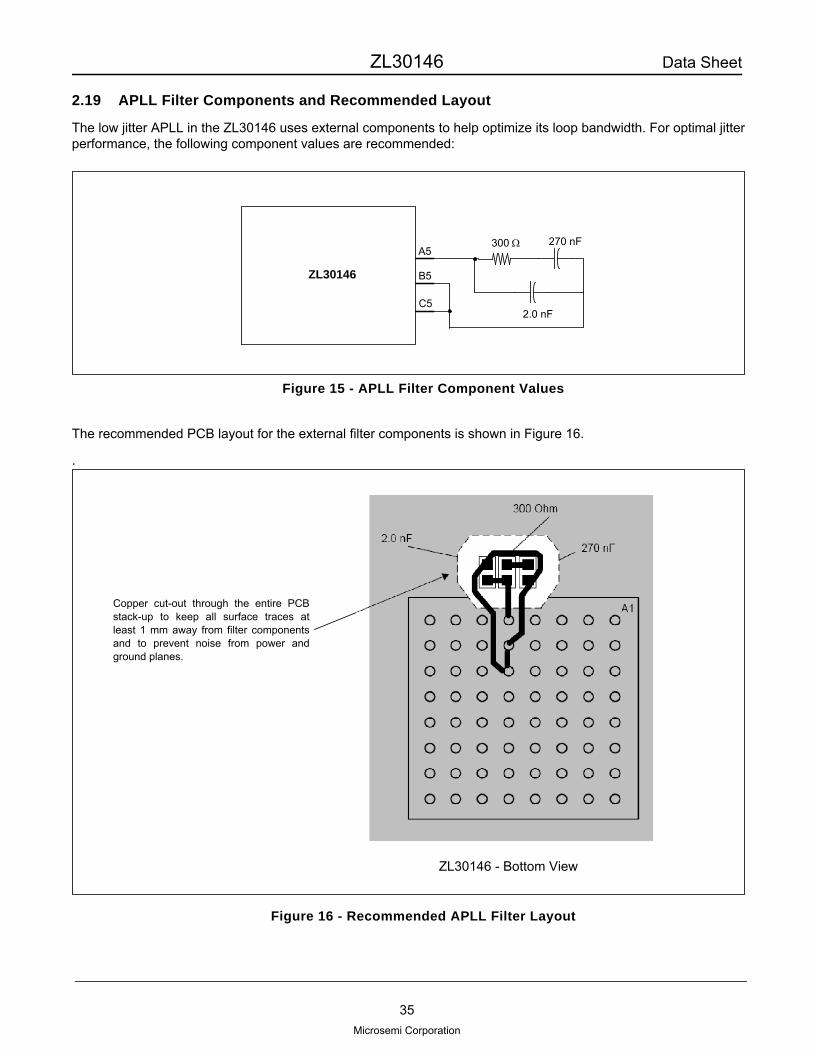
2.19 APLL Filter Components and Recommended Layout
The low jitter APLL in the ZL30146 uses external components to help optimize its loop bandwidth. For optimal jitterperformance, the following component values are recommended:
Figure 15 - APLL Filter Component Values
The recommended PCB layout for the external filter components is shown in Figure 16.
.
Figure 16 - Recommended APLL Filter Layout
300 270 nF
2.0 nF
A5
B5
C5
ZL30146
ZL30146 - Bottom View
Copper cut-out through the entire PCBstack-up to keep all surface traces atleast 1 mm away from filter componentsand to prevent noise from power andground planes.
35Microsemi Corporation
ZL30146 Data Sheet
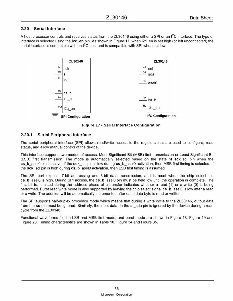
2.20 Serial Interface
A host processor controls and receives status from the ZL30146 using either a SPI or an I2C interface. The type ofinterface is selected using the i2c_en pin. As shown in Figure 17, when i2c_en is set high (or left unconnected) theserial interface is compatible with an I2C bus, and is compatible with SPI when set low.
Figure 17 - Serial Interface Configuration
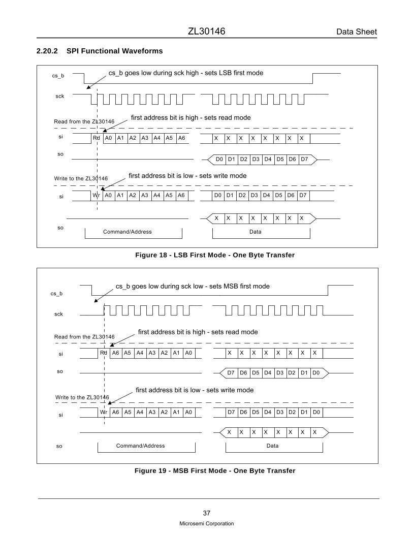
2.20.1 Serial Peripheral Interface
The serial peripheral interface (SPI) allows read/write access to the registers that are used to configure, readstatus, and allow manual control of the device.
This interface supports two modes of access: Most Significant Bit (MSB) first transmission or Least Significant Bit(LSB) first transmission. The mode is automatically selected based on the state of sck_scl pin when thecs_b_asel0 pin is active. If the sck_scl pin is low during cs_b_asel0 activation, then MSB first timing is selected. Ifthe sck_scl pin is high during cs_b_asel0 activation, then LSB first timing is assumed.
The SPI port expects 7-bit addressing and 8-bit data transmission, and is reset when the chip select pincs_b_asel0 is high. During SPI access, the cs_b_asel0 pin must be held low until the operation is complete. Thefirst bit transmitted during the address phase of a transfer indicates whether a read (1) or a write (0) is beingperformed. Burst read/write mode is also supported by leaving the chip select signal cs_b_asel0 is low after a reador a write. The address will be automatically incremented after each data byte is read or written.
The SPI supports half-duplex processor mode which means that during a write cycle to the ZL30146, output datafrom the so pin must be ignored. Similarly, the input data on the si_sda pin is ignored by the device during a readcycle from the ZL30146.
Functional waveforms for the LSB and MSB first mode, and burst mode are shown in Figure 18, Figure 19 andFigure 20. Timing characteristics are shown in Table 10, Figure 34 and Figure 35.
C1 sckD2 siD1 so
C2 cs_bE2 int_b
H2 i2c_en
SPI Configuration
ZL30146C1 sclD2 sda
C2 asel0
H2 i2c_en
I2C Configuration
ZL30146
E2 int_b
36Microsemi Corporation
ZL30146 Data Sheet
2.20.2 SPI Functional Waveforms
Figure 18 - LSB First Mode - One Byte Transfer
Figure 19 - MSB First Mode - One Byte Transfer
cs_b
sck
Read from the ZL30146
Rd A0 A1 A2 A3 A4 A5 A6
D0 D1 D2 D3 D4 D5 D6 D7
Write to the ZL30146
Wr A0 A1 A2 A3 A4 A5 A6 D0 D1 D2 D3 D4 D5 D6 D7
si
si
so
X X X X X X X X
Command/Address Data
X X X X X X X Xso
cs_b goes low during sck high - sets LSB first mode
first address bit is high - sets read mode
first address bit is low - sets write mode
Rd A6 A5 A4 A3 A2 A1 A0 X X X X X X X X
D7 D6 D5 D4 D3 D2 D1 D0
Command/Address Data
Wr A6 A5 A4 A3 A2 A1 A0 D7 D6 D5 D4 D3 D2 D1 D0
X X X X X X X X
cs_b
sck
si
si
so
so
Read from the ZL30146
Write to the ZL30146
cs_b goes low during sck low - sets MSB first mode
first address bit is high - sets read mode
first address bit is low - sets write mode
37Microsemi Corporation
ZL30146 Data Sheet
Figure 20 - Example of a Burst Mode Operation
2.20.3 I2C Interface
The I2C controller supports version 2.1 (January 2000) of the Philips I2C bus specification. The port operates inslave mode with 7-bit addressing, and can operate in Standard (100 kbits/s) and Fast (400 kbits/s) mode. Burstmode is supported in both standard and fast modes.
Data is transferred MSB first and occurs in 1 byte blocks. As shown in Figure 21, a write command consists of a 7-bit device (slave) address, a 7-bit register address (0x00 - 0x7F), and 8-bits of data.
Figure 21 - I2C Data Write Protocol
A read is performed in two stages. A data write is used to set the register address, then a data read is performed toretrieve the data from the set address. This is shown in Figure 22.
Figure 22 - I2C Data Write Protocol
cs_b
Address Data
Address +0
Data
Address +1
Data
Address +2
Data
Address +N
S Slv Addr[6:0] W ACK Reg Addr[6:0]x ACK Data[7:0] ACK PData Write
Byte Byte Byte
S
P
Start (master)
Stop (master)
ACK Acknowledge
Master Initiated
Slave Initiated
W Write
R Read
S Slv Addr[6:0] W ACK Reg Addr[6:0]x ACK P(set read address)
S Slv Addr[6:0] R ACK Data[7:0] ACK PData Read
Byte Byte
Data Write
38Microsemi Corporation
ZL30146 Data Sheet
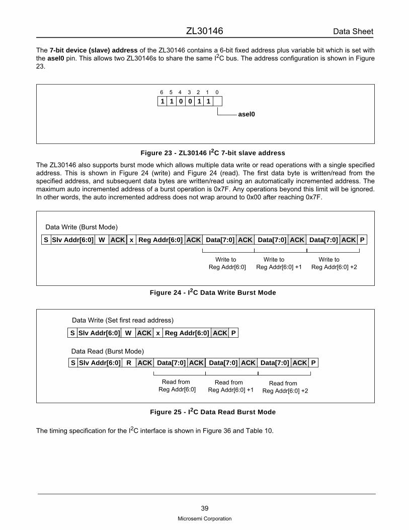
The 7-bit device (slave) address of the ZL30146 contains a 6-bit fixed address plus variable bit which is set withthe asel0 pin. This allows two ZL30146s to share the same I2C bus. The address configuration is shown in Figure23.
Figure 23 - ZL30146 I2C 7-bit slave address
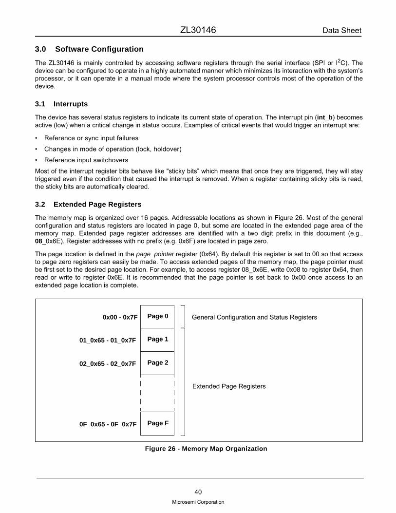
The ZL30146 also supports burst mode which allows multiple data write or read operations with a single specifiedaddress. This is shown in Figure 24 (write) and Figure 24 (read). The first data byte is written/read from thespecified address, and subsequent data bytes are written/read using an automatically incremented address. Themaximum auto incremented address of a burst operation is 0x7F. Any operations beyond this limit will be ignored.In other words, the auto incremented address does not wrap around to 0x00 after reaching 0x7F.
Figure 24 - I2C Data Write Burst Mode
Figure 25 - I2C Data Read Burst Mode
The timing specification for the I2C interface is shown in Figure 36 and Table 10.
1 1 0 00123456
asel0
1 1
S Slv Addr[6:0] W ACK Reg Addr[6:0]x ACK Data[7:0] ACK
Data Write (Burst Mode)
Data[7:0] ACK PData[7:0] ACK
Write toReg Addr[6:0]
Write toReg Addr[6:0] +1
Write toReg Addr[6:0] +2
S Slv Addr[6:0] W ACK Reg Addr[6:0]x ACK
Data[7:0] ACK
Data Write (Set first read address)
Data[7:0] ACK PData[7:0] ACK
Read fromReg Addr[6:0]
P
S Slv Addr[6:0] R ACK
Read fromReg Addr[6:0] +1
Read fromReg Addr[6:0] +2
Data Read (Burst Mode)
39Microsemi Corporation
ZL30146 Data Sheet
3.0 Software ConfigurationThe ZL30146 is mainly controlled by accessing software registers through the serial interface (SPI or I2C). Thedevice can be configured to operate in a highly automated manner which minimizes its interaction with the system’sprocessor, or it can operate in a manual mode where the system processor controls most of the operation of thedevice.
3.1 Interrupts
The device has several status registers to indicate its current state of operation. The interrupt pin (int_b) becomesactive (low) when a critical change in status occurs. Examples of critical events that would trigger an interrupt are:
• Reference or sync input failures
• Changes in mode of operation (lock, holdover)
• Reference input switchovers
Most of the interrupt register bits behave like "sticky bits” which means that once they are triggered, they will staytriggered even if the condition that caused the interrupt is removed. When a register containing sticky bits is read,the sticky bits are automatically cleared.
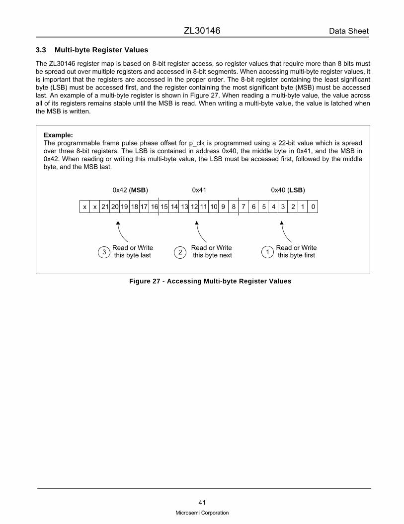
3.2 Extended Page Registers
The memory map is organized over 16 pages. Addressable locations as shown in Figure 26. Most of the generalconfiguration and status registers are located in page 0, but some are located in the extended page area of thememory map. Extended page register addresses are identified with a two digit prefix in this document (e.g.,08_0x6E). Register addresses with no prefix (e.g. 0x6F) are located in page zero.
The page location is defined in the page_pointer register (0x64). By default this register is set to 00 so that accessto page zero registers can easily be made. To access extended pages of the memory map, the page pointer mustbe first set to the desired page location. For example, to access register 08_0x6E, write 0x08 to register 0x64, thenread or write to register 0x6E. It is recommended that the page pointer is set back to 0x00 once access to anextended page location is complete.
Figure 26 - Memory Map Organization
Page 00x00 - 0x7F
Page 101_0x65 - 01_0x7F
Page 202_0x65 - 02_0x7F
Page F0F_0x65 - 0F_0x7F
Extended Page Registers
General Configuration and Status Registers
40Microsemi Corporation
ZL30146 Data Sheet
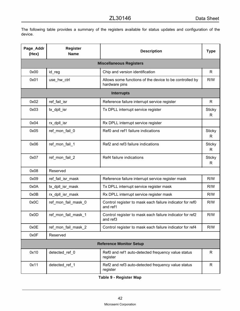
3.3 Multi-byte Register Values
The ZL30146 register map is based on 8-bit register access, so register values that require more than 8 bits mustbe spread out over multiple registers and accessed in 8-bit segments. When accessing multi-byte register values, itis important that the registers are accessed in the proper order. The 8-bit register containing the least significantbyte (LSB) must be accessed first, and the register containing the most significant byte (MSB) must be accessedlast. An example of a multi-byte register is shown in Figure 27. When reading a multi-byte value, the value acrossall of its registers remains stable until the MSB is read. When writing a multi-byte value, the value is latched whenthe MSB is written.
Figure 27 - Accessing Multi-byte Register Values
017 6 5 4 3 28915 14 13 12 11 101617x x 21 20 19 18
0x40 (LSB)0x410x42 (MSB)
Read or Write this byte first
Read or Write this byte next
Read or Write this byte last 123
Example:The programmable frame pulse phase offset for p_clk is programmed using a 22-bit value which is spreadover three 8-bit registers. The LSB is contained in address 0x40, the middle byte in 0x41, and the MSB in0x42. When reading or writing this multi-byte value, the LSB must be accessed first, followed by the middlebyte, and the MSB last.
41Microsemi Corporation
ZL30146 Data Sheet
The following table provides a summary of the registers available for status updates and configuration of thedevice.
.
Page_Addr(Hex)
RegisterName
Description Type
Miscellaneous Registers
0x00 id_reg Chip and version identification R
0x01 use_hw_ctrl Allows some functions of the device to be controlled by hardware pins
R/W
Interrupts
0x02 ref_fail_isr Reference failure interrupt service register R
0x03 tx_dpll_isr Tx DPLL interrupt service register StickyR
0x04 rx_dpll_isr Rx DPLL interrupt service register
0x05 ref_mon_fail_0 Ref0 and ref1 failure indications Sticky R
0x06 ref_mon_fail_1 Ref2 and ref3 failure indications Sticky R
0x07 ref_mon_fail_2 Ref4 failure indications Sticky R
0x08 Reserved
0x09 ref_fail_isr_mask Reference failure interrupt service register mask R/W
0x0A tx_dpll_isr_mask Tx DPLL interrupt service register mask R/W
0x0B rx_dpll_isr_mask Rx DPLL interrupt service register mask R/W
0x0C ref_mon_fail_mask_0 Control register to mask each failure indicator for ref0 and ref1
R/W
0x0D ref_mon_fail_mask_1 Control register to mask each failure indicator for ref2 and ref3
R/W
0x0E ref_mon_fail_mask_2 Control register to mask each failure indicator for ref4 R/W
0x0F Reserved
Reference Monitor Setup
0x10 detected_ref_0 Ref0 and ref1 auto-detected frequency value status register
R
0x11 detected_ref_1 Ref2 and ref3 auto-detected frequency value status register
R
Table 9 - Register Map
42Microsemi Corporation
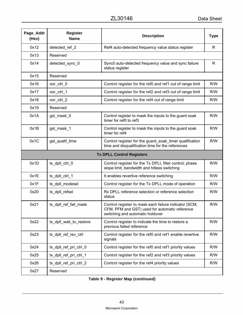
ZL30146 Data Sheet
0x12 detected_ref_2 Ref4 auto-detected frequency value status register R
0x13 Reserved
0x14 detected_sync_0 Sync0 auto-detected frequency value and sync failure status register
R
0x15 Reserved
0x16 oor_ctrl_0 Control register for the ref0 and ref1 out of range limit R/W
0x17 oor_ctrl_1 Control register for the ref2 and ref3 out of range limit R/W
0x18 oor_ctrl_2 Control register for the ref4 out of range limit R/W
0x19 Reserved
0x1A gst_mask_0 Control register to mask the inputs to the guard soak timer for ref0 to ref3
R/W
0x1B gst_mask_1 Control register to mask the inputs to the guard soak timer for ref4
R/W
0x1C gst_qualif_time Control register for the guard_soak_timer qualification time and disqualification time for the references
R/W
Tx DPLL Control Registers
0x1D tx_dpll_ctrl_0 Control register for the Tx DPLL filter control; phase slope limit, bandwidth and hitless switching
R/W
0x1E tx_dpll_ctrl_1 It enables revertive reference switching R/W
0x1F tx_dpll_modesel Control register for the Tx DPLL mode of operation R/W
0x20 tx_dpll_refsel Rx DPLL reference selection or reference selection status
R/W
0x21 tx_dpll_ref_fail_mask Control register to mask each failure indicator (SCM, CFM, PFM and GST) used for automatic reference switching and automatic holdover
R/W
0x22 tx_dpll_wait_to_restore Control register to indicate the time to restore a previous failed reference
R/W
0x23 tx_dpll_ref_rev_ctrl Control register for the ref0 and ref1 enable revertive signals
R/W
0x24 tx_dpll_ref_pri_ctrl_0 Control register for the ref0 and ref1 priority values R/W
0x25 tx_dpll_ref_pri_ctrl_1 Control register for the ref2 and ref3 priority values R/W
0x26 tx_dpll_ref_pri_ctrl_2 Control register for the ref4 priority values R/W
0x27 Reserved
Page_Addr(Hex)
RegisterName
Description Type
Table 9 - Register Map (continued)
43Microsemi Corporation
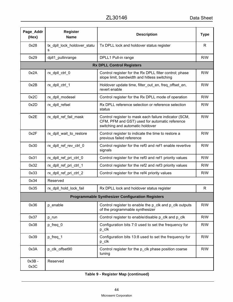
ZL30146 Data Sheet
0x28 tx_dpll_lock_holdover_status
Tx DPLL lock and holdover status register R
0x29 dpll1_pullinrange DPLL1 Pull-in range R/W
Rx DPLL Control Registers
0x2A rx_dpll_ctrl_0 Control register for the Rx DPLL filter control; phase slope limit, bandwidth and hitless switching
R/W
0x2B rx_dpll_ctrl_1 Holdover update time, filter_out_en, freq_offset_en, revert enable
R/W
0x2C rx_dpll_modesel Control register for the Rx DPLL mode of operation R/W
0x2D rx_dpll_refsel Rx DPLL reference selection or reference selection status
R/W
0x2E rx_dpll_ref_fail_mask Control register to mask each failure indicator (SCM, CFM, PFM and GST) used for automatic reference switching and automatic holdover
R/W
0x2F rx_dpll_wait_to_restore Control register to indicate the time to restore a previous failed reference
R/W
0x30 rx_dpll_ref_rev_ctrl_0 Control register for the ref0 and ref1 enable revertive signals
R/W
0x31 rx_dpll_ref_pri_ctrl_0 Control register for the ref0 and ref1 priority values R/W
0x32 rx_dpll_ref_pri_ctrl_1 Control register for the ref2 and ref3 priority values R/W
0x33 rx_dpll_ref_pri_ctrl_2 Control register for the ref4 priority values R/W
0x34 Reserved
0x35 rx_dpll_hold_lock_fail Rx DPLL lock and holdover status register R
Programmable Synthesizer Configuration Registers
0x36 p_enable Control register to enable the p_clk and p_clk outputs of the programmable synthesizer
R/W
0x37 p_run Control register to enable/disable p_clk and p_clk R/W
0x38 p_freq_0 Configuration bits 7:0 used to set the frequency for p_clk
R/W
0x39 p_freq_1 Configuration bits 13:8 used to set the frequency for p_clk
R/W
0x3A p_clk_offset90 Control register for the p_clk phase position coarse tuning
R/W
0x3B - 0x3C
Reserved
Page_Addr(Hex)
RegisterName
Description Type
Table 9 - Register Map (continued)
44Microsemi Corporation
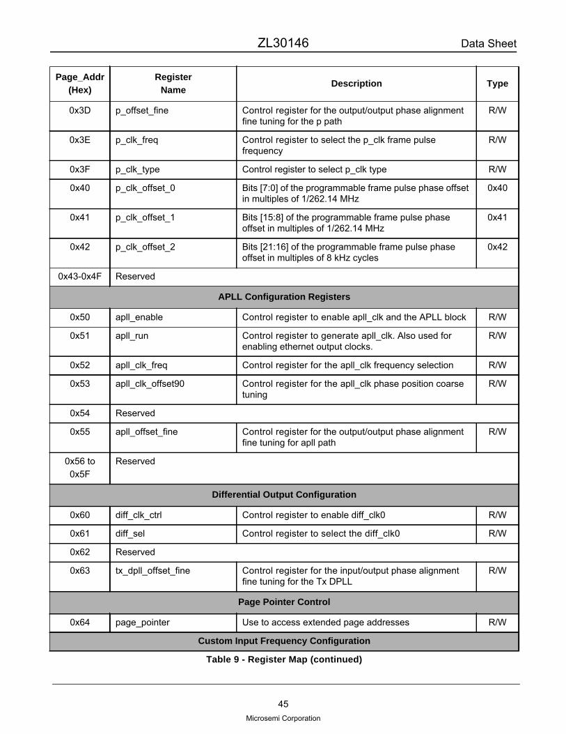
ZL30146 Data Sheet
0x3D p_offset_fine Control register for the output/output phase alignment fine tuning for the p path
R/W
0x3E p_clk_freq Control register to select the p_clk frame pulse frequency
R/W
0x3F p_clk_type Control register to select p_clk type R/W
0x40 p_clk_offset_0 Bits [7:0] of the programmable frame pulse phase offset in multiples of 1/262.14 MHz
0x40
0x41 p_clk_offset_1 Bits [15:8] of the programmable frame pulse phase offset in multiples of 1/262.14 MHz
0x41
0x42 p_clk_offset_2 Bits [21:16] of the programmable frame pulse phase offset in multiples of 8 kHz cycles
0x42
0x43-0x4F Reserved
APLL Configuration Registers
0x50 apll_enable Control register to enable apll_clk and the APLL block R/W
0x51 apll_run Control register to generate apll_clk. Also used for enabling ethernet output clocks.
R/W
0x52 apll_clk_freq Control register for the apll_clk frequency selection R/W
0x53 apll_clk_offset90 Control register for the apll_clk phase position coarse tuning
R/W
0x54 Reserved
0x55 apll_offset_fine Control register for the output/output phase alignment fine tuning for apll path
R/W
0x56 to 0x5F
Reserved
Differential Output Configuration
0x60 diff_clk_ctrl Control register to enable diff_clk0 R/W
0x61 diff_sel Control register to select the diff_clk0 R/W
0x62 Reserved
0x63 tx_dpll_offset_fine Control register for the input/output phase alignment fine tuning for the Tx DPLL
R/W
Page Pointer Control
0x64 page_pointer Use to access extended page addresses R/W
Custom Input Frequency Configuration
Page_Addr(Hex)
RegisterName
Description Type
Table 9 - Register Map (continued)
45Microsemi Corporation
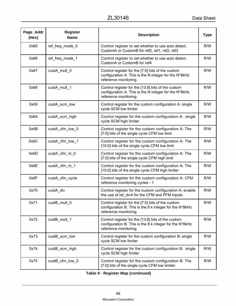
ZL30146 Data Sheet
0x65 ref_freq_mode_0 Control register to set whether to use auto detect, CustomA or CustomB for ref0, ref1, ref2, ref3
R/W
0x66 ref_freq_mode_1 Control register to set whether to use auto detect, CustomA or CustomB for ref4
R/W
0x67 custA_mult_0 Control register for the [7:0] bits of the custom configuration A. This is the N integer for the N*8kHz reference monitoring.
R/W
0x68 custA_mult_1 Control register for the [13:8] bits of the custom configuration A. This is the N integer for the N*8kHz reference monitoring.
R/W
0x69 custA_scm_low Control register for the custom configuration A: single cycle SCM low limiter
R/W
0x6A custA_scm_high Control register for the custom configuration A: single cycle SCM high limiter
R/W
0x6B custA_cfm_low_0 Control register for the custom configuration A: The [7:0] bits of the single cycle CFM low limit
R/W
0x6C custA_cfm_low_1 Control register for the custom configuration A: The [15:0] bits of the single cycle CFM low limit
R/W
0x6D custA_cfm_hi_0 Control register for the custom configuration A: The [7:0] bits of the single cycle CFM high limit
R/W
0x6E custA_cfm_hi_1 Control register for the custom configuration A: The [15:0] bits of the single cycle CFM high limiter
R/W
0x6F custA_cfm_cycle Control register for the custom configuration A: CFM reference monitoring cycles - 1
R/W
0x70 custA_div Control register for the custom configuration A: enable the use of ref_div4 for the CFM and PFM inputs
R/W
0x71 custB_mult_0 Control register for the [7:0] bits of the custom configuration B. This is the 8 k integer for the N*8kHz reference monitoring.
R/W
0x72 custB_mult_1 Control register for the [13:8] bits of the custom configuration B. This is the 8 k integer for the N*8kHz reference monitoring.
R/W
0x73 custB_scm_low Control register for the custom configuration B: single cycle SCM low limiter
R/W
0x74 custB_scm_high Control register for the custom configuration B: single cycle SCM high limiter
R/W
0x75 custB_cfm_low_0 Control register for the custom configuration B: The [7:0] bits of the single cycle CFM low limiter.
R/W
Page_Addr(Hex)
RegisterName
Description Type
Table 9 - Register Map (continued)
46Microsemi Corporation
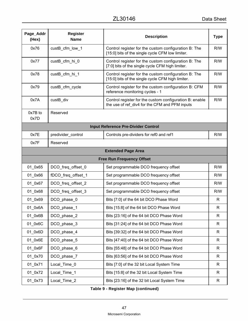
ZL30146 Data Sheet
0x76 custB_cfm_low_1 Control register for the custom configuration B: The [15:0] bits of the single cycle CFM low limiter.
R/W
0x77 custB_cfm_hi_0 Control register for the custom configuration B: The [7:0] bits of the single cycle CFM high limiter.
R/W
0x78 custB_cfm_hi_1 Control register for the custom configuration B: The [15:0] bits of the single cycle CFM high limiter.
R/W
0x79 custB_cfm_cycle Control register for the custom configuration B: CFM reference monitoring cycles - 1
R/W
0x7A custB_div Control register for the custom configuration B: enable the use of ref_div4 for the CFM and PFM inputs
R/W
0x7B to 0x7D
Reserved
Input Reference Pre-Divider Control
0x7E predivider_control Controls pre-dividers for ref0 and ref1 R/W
0x7F Reserved
Extended Page Area
Free Run Frequency Offset
01_0x65 DCO_freq_offset_0 Set programmable DCO frequency offset R/W
01_0x66 fDCO_freq_offset_1 Set programmable DCO frequency offset R/W
01_0x67 DCO_freq_offset_2 Set programmable DCO frequency offset R/W
01_0x68 DCO_freq_offset_3 Set programmable DCO frequency offset R/W
01_0x69 DCO_phase_0 Bits [7:0] of the 64 bit DCO Phase Word R
01_0x6A DCO_phase_1 Bits [15:8] of the 64 bit DCO Phase Word R
01_0x6B DCO_phase_2 Bits [23:16] of the 64 bit DCO Phase Word R
01_0x6C DCO_phase_3 Bits [31:24] of the 64 bit DCO Phase Word R
01_0x6D DCO_phase_4 Bits [39:32] of the 64 bit DCO Phase Word R
01_0x6E DCO_phase_5 Bits [47:40] of the 64 bit DCO Phase Word R
01_0x6F DCO_phase_6 Bits [55:48] of the 64 bit DCO Phase Word R
01_0x70 DCO_phase_7 Bits [63:56] of the 64 bit DCO Phase Word R
01_0x71 Local_Time_0 Bits [7:0] of the 32 bit Local System Time R
01_0x72 Local_Time_1 Bits [15:8] of the 32 bit Local System Time R
01_0x73 Local_Time_2 Bits [23:16] of the 32 bit Local System Time R
Page_Addr(Hex)
RegisterName
Description Type
Table 9 - Register Map (continued)
47Microsemi Corporation
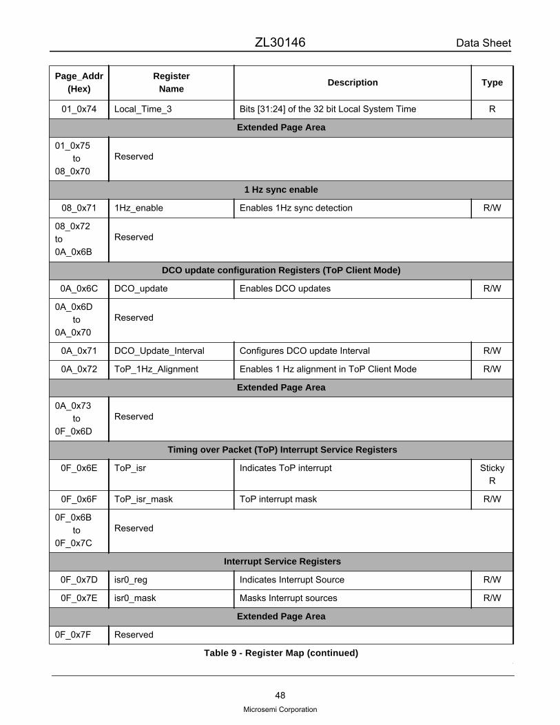
ZL30146 Data Sheet
.
01_0x74 Local_Time_3 Bits [31:24] of the 32 bit Local System Time R
Extended Page Area
01_0x75 to 08_0x70
Reserved
1 Hz sync enable
08_0x71 1Hz_enable Enables 1Hz sync detection R/W
08_0x72 to 0A_0x6B
Reserved
DCO update configuration Registers (ToP Client Mode)
0A_0x6C DCO_update Enables DCO updates R/W
0A_0x6D to 0A_0x70
Reserved
0A_0x71 DCO_Update_Interval Configures DCO update Interval R/W
0A_0x72 ToP_1Hz_Alignment Enables 1 Hz alignment in ToP Client Mode R/W
Extended Page Area
0A_0x73 to 0F_0x6D
Reserved
Timing over Packet (ToP) Interrupt Service Registers
0F_0x6E ToP_isr Indicates ToP interrupt Sticky R
0F_0x6F ToP_isr_mask ToP interrupt mask R/W
0F_0x6B to 0F_0x7C
Reserved
Interrupt Service Registers
0F_0x7D isr0_reg Indicates Interrupt Source R/W
0F_0x7E isr0_mask Masks Interrupt sources R/W
Extended Page Area
0F_0x7F Reserved
Page_Addr(Hex)
RegisterName
Description Type
Table 9 - Register Map (continued)
48Microsemi Corporation
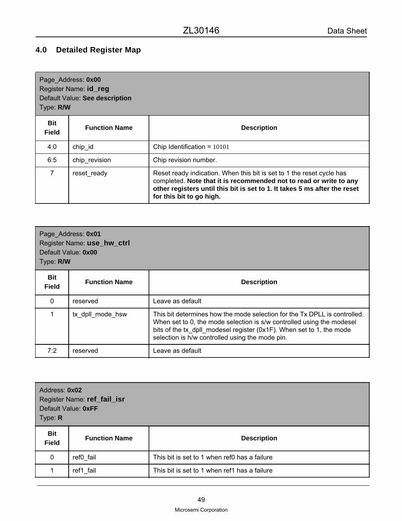
ZL30146 Data Sheet
4.0 Detailed Register Map
Page_Address: 0x00Register Name: id_regDefault Value: See descriptionType: R/W
Bit Field
Function Name Description
4:0 chip_id Chip Identification = 10101
6:5 chip_revision Chip revision number.
7 reset_ready Reset ready indication. When this bit is set to 1 the reset cycle has completed. Note that it is recommended not to read or write to any other registers until this bit is set to 1. It takes 5 ms after the reset for this bit to go high.
Page_Address: 0x01Register Name: use_hw_ctrlDefault Value: 0x00Type: R/W
Bit Field
Function Name Description
0 reserved Leave as default
1 tx_dpll_mode_hsw This bit determines how the mode selection for the Tx DPLL is controlled. When set to 0, the mode selection is s/w controlled using the modesel bits of the tx_dpll_modesel register (0x1F). When set to 1, the mode selection is h/w controlled using the mode pin.
7:2 reserved Leave as default
Address: 0x02Register Name: ref_fail_isrDefault Value: 0xFFType: R
Bit Field
Function Name Description
0 ref0_fail This bit is set to 1 when ref0 has a failure
1 ref1_fail This bit is set to 1 when ref1 has a failure
49Microsemi Corporation
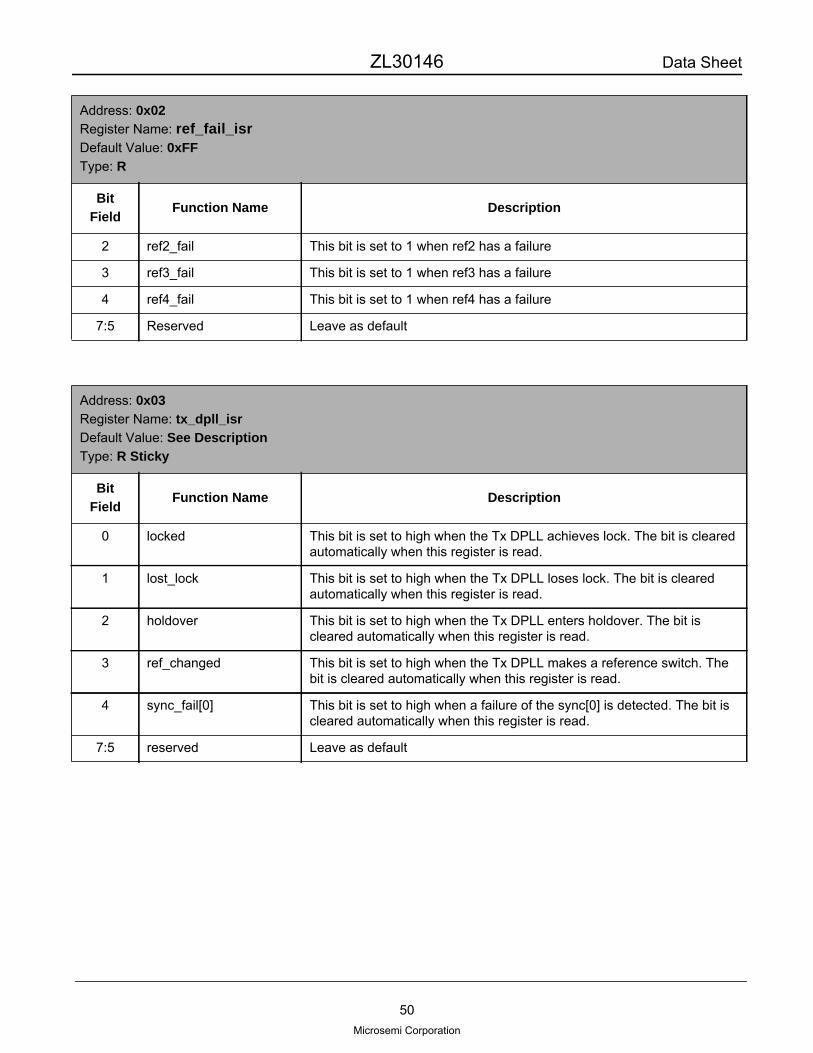
ZL30146 Data Sheet
2 ref2_fail This bit is set to 1 when ref2 has a failure
3 ref3_fail This bit is set to 1 when ref3 has a failure
4 ref4_fail This bit is set to 1 when ref4 has a failure
7:5 Reserved Leave as default
Address: 0x03Register Name: tx_dpll_isrDefault Value: See DescriptionType: R Sticky
Bit Field
Function Name Description
0 locked This bit is set to high when the Tx DPLL achieves lock. The bit is cleared automatically when this register is read.
1 lost_lock This bit is set to high when the Tx DPLL loses lock. The bit is cleared automatically when this register is read.
2 holdover This bit is set to high when the Tx DPLL enters holdover. The bit is cleared automatically when this register is read.
3 ref_changed This bit is set to high when the Tx DPLL makes a reference switch. The bit is cleared automatically when this register is read.
4 sync_fail[0] This bit is set to high when a failure of the sync[0] is detected. The bit is cleared automatically when this register is read.
7:5 reserved Leave as default
Address: 0x02Register Name: ref_fail_isrDefault Value: 0xFFType: R
Bit Field
Function Name Description
50Microsemi Corporation
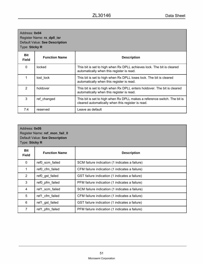
ZL30146 Data Sheet
Address: 0x04Register Name: rx_dpll_isrDefault Value: See DescriptionType: Sticky R
Bit Field
Function Name Description
0 locked This bit is set to high when Rx DPLL achieves lock. The bit is cleared automatically when this register is read.
1 lost_lock This bit is set to high when Rx DPLL loses lock. The bit is cleared automatically when this register is read.
2 holdover This bit is set to high when Rx DPLL enters holdover. The bit is cleared automatically when this register is read.
3 ref_changed This bit is set to high when Rx DPLL makes a reference switch. The bit is cleared automatically when this register is read.
7:4 reserved Leave as default
Address: 0x05Register Name: ref_mon_fail_0Default Value: See DescriptionType: Sticky R
Bit Field
Function Name Description
0 ref0_scm_failed SCM failure indication (1 indicates a failure)
1 ref0_cfm_failed CFM failure indication (1 indicates a failure)
2 ref0_gst_failed GST failure indication (1 indicates a failure)
3 ref0_pfm_failed PFM failure indication (1 indicates a failure)
4 ref1_scm_failed SCM failure indication (1 indicates a failure)
5 ref1_cfm_failed CFM failure indication (1 indicates a failure)
6 ref1_gst_failed GST failure indication (1 indicates a failure)
7 ref1_pfm_failed PFM failure indication (1 indicates a failure)
51Microsemi Corporation
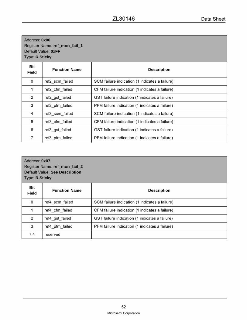
ZL30146 Data Sheet
Address: 0x06Register Name: ref_mon_fail_1Default Value: 0xFFType: R Sticky
Bit Field
Function Name Description
0 ref2_scm_failed SCM failure indication (1 indicates a failure)
1 ref2_cfm_failed CFM failure indication (1 indicates a failure)
2 ref2_gst_failed GST failure indication (1 indicates a failure)
3 ref2_pfm_failed PFM failure indication (1 indicates a failure)
4 ref3_scm_failed SCM failure indication (1 indicates a failure)
5 ref3_cfm_failed CFM failure indication (1 indicates a failure)
6 ref3_gst_failed GST failure indication (1 indicates a failure)
7 ref3_pfm_failed PFM failure indication (1 indicates a failure)
Address: 0x07Register Name: ref_mon_fail_2Default Value: See DescriptionType: R Sticky
Bit Field
Function Name Description
0 ref4_scm_failed SCM failure indication (1 indicates a failure)
1 ref4_cfm_failed CFM failure indication (1 indicates a failure)
2 ref4_gst_failed GST failure indication (1 indicates a failure)
3 ref4_pfm_failed PFM failure indication (1 indicates a failure)
7:4 reserved
52Microsemi Corporation
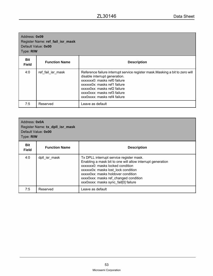
ZL30146 Data Sheet
Address: 0x09Register Name: ref_fail_isr_maskDefault Value: 0x00Type: R/W
Bit Field
Function Name Description
4:0 ref_fail_isr_mask Reference failure interrupt service register mask.Masking a bit to zero will disable interrupt generation.xxxxxxx0: masks ref0 failure xxxxxx0x: masks ref1 failure xxxxx0xx: masks ref2 failure xxxx0xxx: masks ref3 failure xxx0xxxx: masks ref4 failure
7:5 Reserved Leave as default
Address: 0x0ARegister Name: tx_dpll_isr_maskDefault Value: 0x00Type: R/W
Bit Field
Function Name Description
4:0 dpll_isr_mask Tx DPLL interrupt service register mask.Enabling a mask bit to one will allow interrupt generationxxxxxxx0: masks locked condition xxxxxx0x: masks lost_lock condition xxxxx0xx: masks holdover condition xxxx0xxx: masks ref_changed condition xxx0xxxx: masks sync_fail[0] failure
7:5 Reserved Leave as default
53Microsemi Corporation
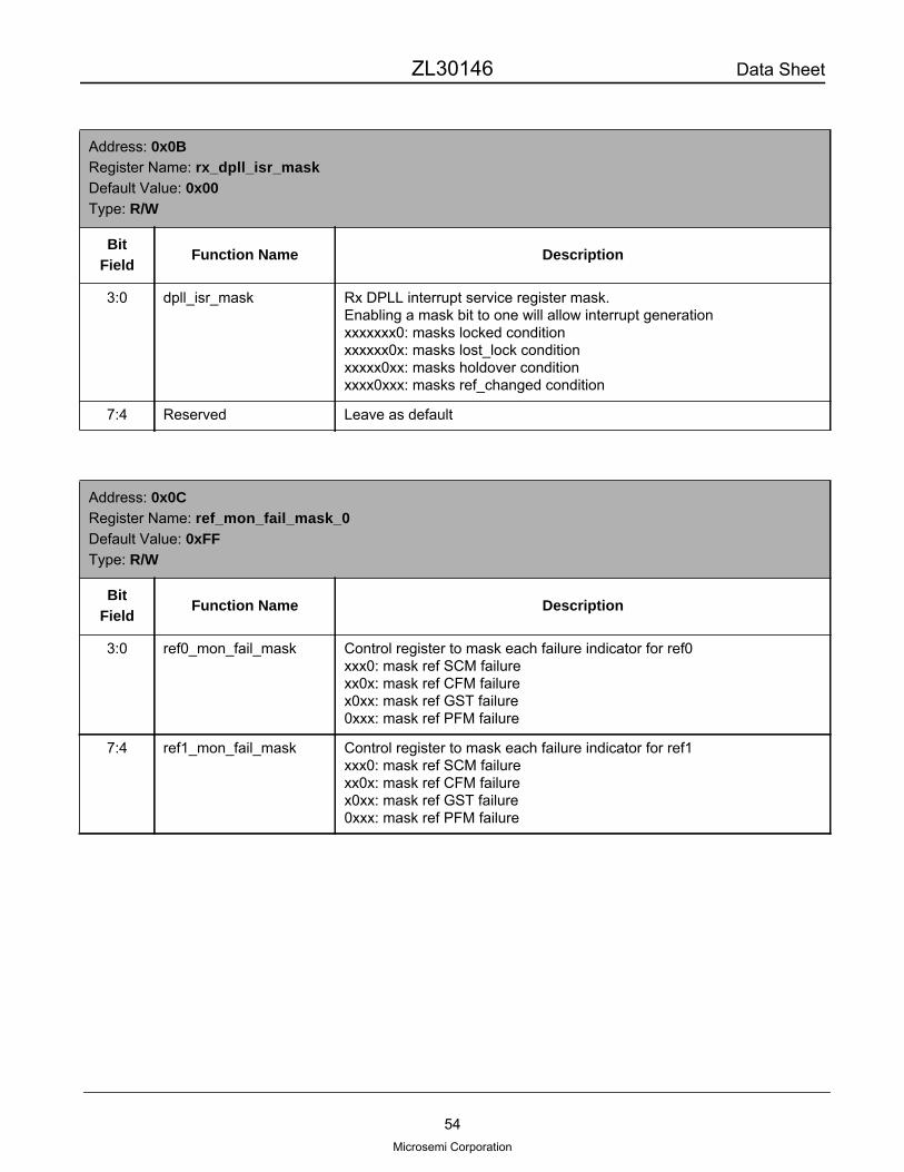
ZL30146 Data Sheet
Address: 0x0BRegister Name: rx_dpll_isr_maskDefault Value: 0x00Type: R/W
Bit Field
Function Name Description
3:0 dpll_isr_mask Rx DPLL interrupt service register mask.Enabling a mask bit to one will allow interrupt generationxxxxxxx0: masks locked condition xxxxxx0x: masks lost_lock condition xxxxx0xx: masks holdover condition xxxx0xxx: masks ref_changed condition
7:4 Reserved Leave as default
Address: 0x0CRegister Name: ref_mon_fail_mask_0Default Value: 0xFFType: R/W
Bit Field
Function Name Description
3:0 ref0_mon_fail_mask Control register to mask each failure indicator for ref0xxx0: mask ref SCM failurexx0x: mask ref CFM failurex0xx: mask ref GST failure0xxx: mask ref PFM failure
7:4 ref1_mon_fail_mask Control register to mask each failure indicator for ref1xxx0: mask ref SCM failurexx0x: mask ref CFM failurex0xx: mask ref GST failure0xxx: mask ref PFM failure
54Microsemi Corporation
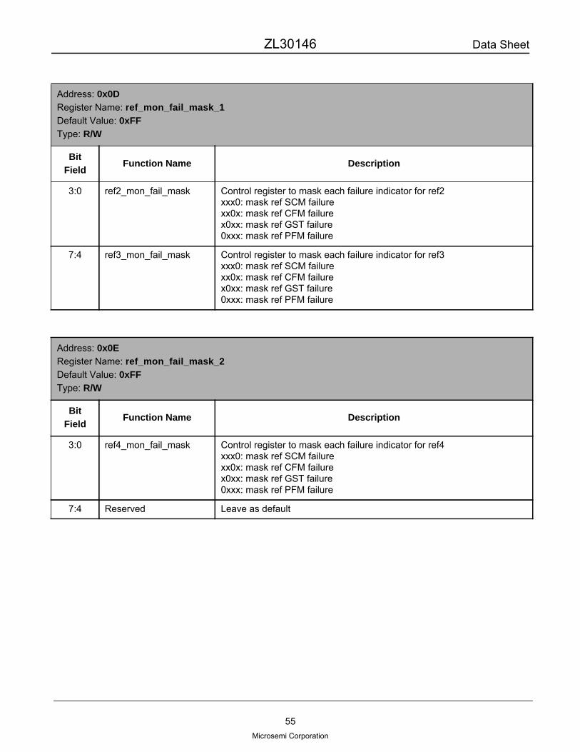
ZL30146 Data Sheet
Address: 0x0DRegister Name: ref_mon_fail_mask_1Default Value: 0xFFType: R/W
Bit Field
Function Name Description
3:0 ref2_mon_fail_mask Control register to mask each failure indicator for ref2xxx0: mask ref SCM failurexx0x: mask ref CFM failurex0xx: mask ref GST failure0xxx: mask ref PFM failure
7:4 ref3_mon_fail_mask Control register to mask each failure indicator for ref3xxx0: mask ref SCM failurexx0x: mask ref CFM failurex0xx: mask ref GST failure0xxx: mask ref PFM failure
Address: 0x0ERegister Name: ref_mon_fail_mask_2Default Value: 0xFFType: R/W
Bit Field
Function Name Description
3:0 ref4_mon_fail_mask Control register to mask each failure indicator for ref4xxx0: mask ref SCM failurexx0x: mask ref CFM failurex0xx: mask ref GST failure0xxx: mask ref PFM failure
7:4 Reserved Leave as default
55Microsemi Corporation

ZL30146 Data Sheet
Address: 0x10Register Name: detected_ref_0Default Value: See DescriptionType: R
Bit Field
Function Name Description
3:0 ref0_frq_detected ref0 auto-detected frequency value 0000: -> 2 kHz 0001: -> 8 kHz0010: -> 64 kHz0011: -> 1.544 MHz0100: -> 2.048 MHz0101: -> 6.48 MHz0110: -> 8.192 MHz0111: -> 16.384 MHz1000: -> 19.44 MHz1001: -> 38.88 MHz1010: -> 77.76 MHz1111:-> Not yet detected
7:4 ref1_frq_detected ref1 auto-detected frequency value 0000: -> 2 kHz 0001: -> 8 kHz0010: -> 64 kHz0011: -> 1.544 MHz0100: -> 2.048 MHz0101: -> 6.48 MHz0110: -> 8.192 MHz0111: -> 16.384 MHz1000: -> 19.44 MHz1001: -> 38.88 MHz1010: -> 77.76 MHz 1111:-> Not yet detected
56Microsemi Corporation
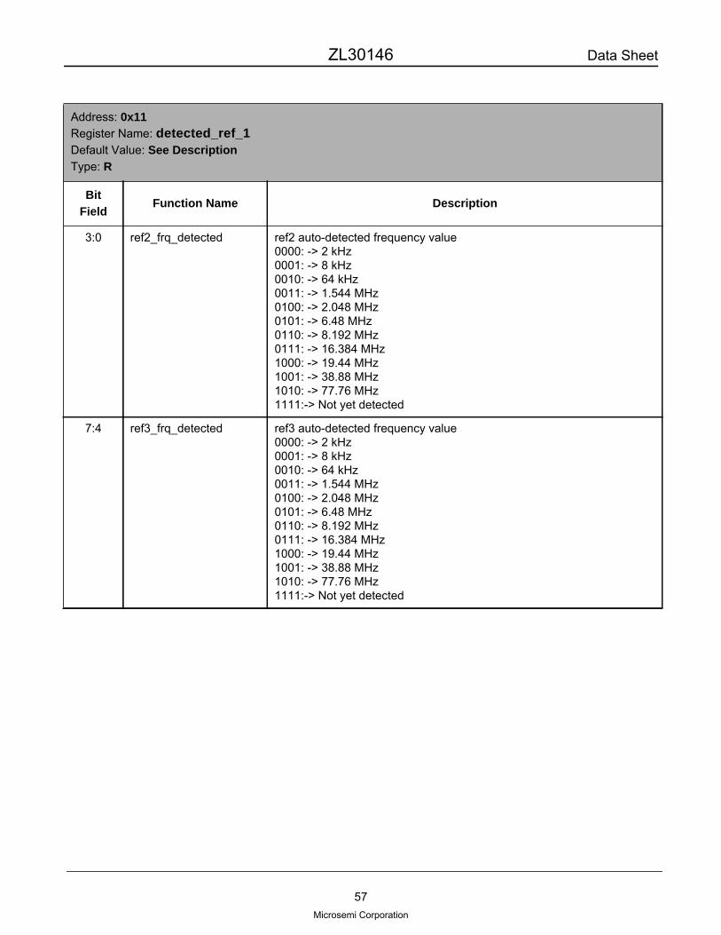
ZL30146 Data Sheet
Address: 0x11Register Name: detected_ref_1Default Value: See DescriptionType: R
Bit Field
Function Name Description
3:0 ref2_frq_detected ref2 auto-detected frequency value 0000: -> 2 kHz 0001: -> 8 kHz0010: -> 64 kHz0011: -> 1.544 MHz0100: -> 2.048 MHz0101: -> 6.48 MHz0110: -> 8.192 MHz0111: -> 16.384 MHz1000: -> 19.44 MHz1001: -> 38.88 MHz1010: -> 77.76 MHz1111:-> Not yet detected
7:4 ref3_frq_detected ref3 auto-detected frequency value 0000: -> 2 kHz 0001: -> 8 kHz0010: -> 64 kHz0011: -> 1.544 MHz0100: -> 2.048 MHz0101: -> 6.48 MHz0110: -> 8.192 MHz0111: -> 16.384 MHz1000: -> 19.44 MHz1001: -> 38.88 MHz1010: -> 77.76 MHz 1111:-> Not yet detected
57Microsemi Corporation
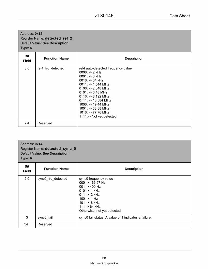
ZL30146 Data Sheet
Address: 0x12Register Name: detected_ref_2Default Value: See DescriptionType: R
Bit Field
Function Name Description
3:0 ref4_frq_detected ref4 auto-detected frequency value 0000: -> 2 kHz 0001: -> 8 kHz0010: -> 64 kHz0011: -> 1.544 MHz0100: -> 2.048 MHz0101: -> 6.48 MHz0110: -> 8.192 MHz0111: -> 16.384 MHz1000: -> 19.44 MHz1001: -> 38.88 MHz1010: -> 77.76 MHz1111:-> Not yet detected
7:4 Reserved
Address: 0x14Register Name: detected_sync_0Default Value: See DescriptionType: R
Bit Field
Function Name Description
2:0 sync0_frq_detected sync0 frequency value 000 -> 166.67 Hz001 -> 400 Hz010 -> 1 kHz 011 -> 2 kHz100 -> 1 Hz101 -> 8 kHz111 -> 64 kHzOtherwise: not yet detected
3 sync0_fail sync0 fail status. A value of 1 indicates a failure.
7:4 Reserved
58Microsemi Corporation
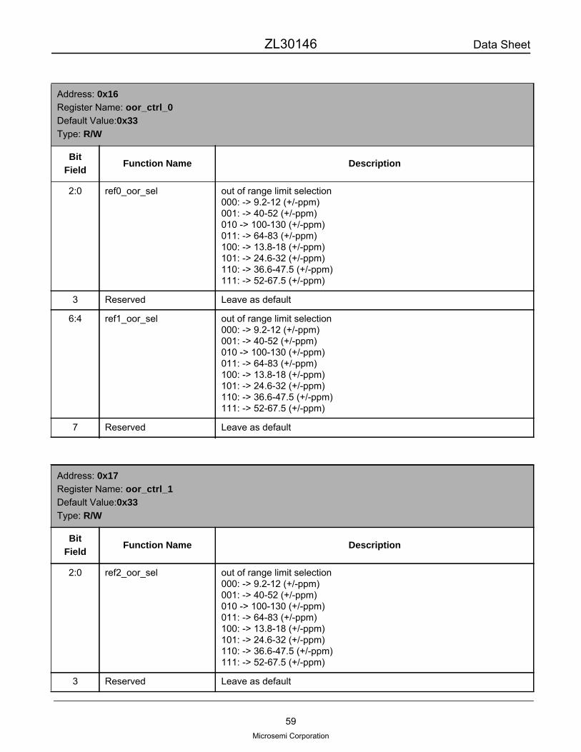
ZL30146 Data Sheet
Address: 0x16Register Name: oor_ctrl_0Default Value:0x33Type: R/W
Bit Field
Function Name Description
2:0 ref0_oor_sel out of range limit selection 000: -> 9.2-12 (+/-ppm) 001: -> 40-52 (+/-ppm) 010 -> 100-130 (+/-ppm)011: -> 64-83 (+/-ppm) 100: -> 13.8-18 (+/-ppm) 101: -> 24.6-32 (+/-ppm) 110: -> 36.6-47.5 (+/-ppm) 111: -> 52-67.5 (+/-ppm)
3 Reserved Leave as default
6:4 ref1_oor_sel out of range limit selection 000: -> 9.2-12 (+/-ppm) 001: -> 40-52 (+/-ppm) 010 -> 100-130 (+/-ppm)011: -> 64-83 (+/-ppm) 100: -> 13.8-18 (+/-ppm) 101: -> 24.6-32 (+/-ppm) 110: -> 36.6-47.5 (+/-ppm) 111: -> 52-67.5 (+/-ppm)
7 Reserved Leave as default
Address: 0x17Register Name: oor_ctrl_1Default Value:0x33Type: R/W
Bit Field
Function Name Description
2:0 ref2_oor_sel out of range limit selection 000: -> 9.2-12 (+/-ppm) 001: -> 40-52 (+/-ppm) 010 -> 100-130 (+/-ppm)011: -> 64-83 (+/-ppm) 100: -> 13.8-18 (+/-ppm) 101: -> 24.6-32 (+/-ppm) 110: -> 36.6-47.5 (+/-ppm) 111: -> 52-67.5 (+/-ppm)
3 Reserved Leave as default
59Microsemi Corporation
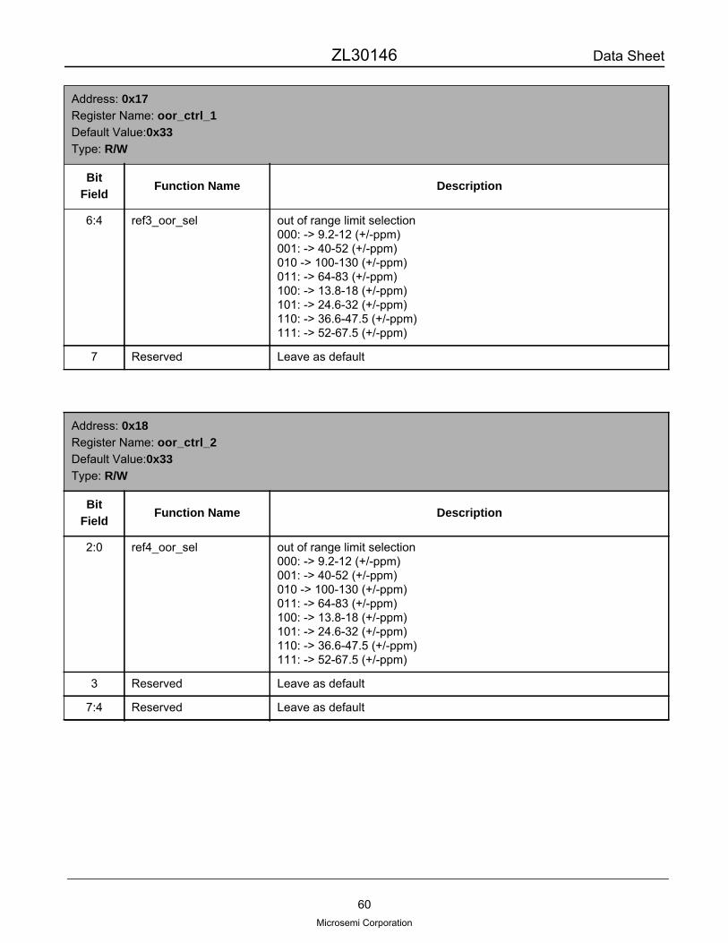
ZL30146 Data Sheet
6:4 ref3_oor_sel out of range limit selection 000: -> 9.2-12 (+/-ppm) 001: -> 40-52 (+/-ppm) 010 -> 100-130 (+/-ppm)011: -> 64-83 (+/-ppm) 100: -> 13.8-18 (+/-ppm) 101: -> 24.6-32 (+/-ppm) 110: -> 36.6-47.5 (+/-ppm) 111: -> 52-67.5 (+/-ppm)
7 Reserved Leave as default
Address: 0x18Register Name: oor_ctrl_2Default Value:0x33Type: R/W
Bit Field
Function Name Description
2:0 ref4_oor_sel out of range limit selection 000: -> 9.2-12 (+/-ppm) 001: -> 40-52 (+/-ppm) 010 -> 100-130 (+/-ppm)011: -> 64-83 (+/-ppm) 100: -> 13.8-18 (+/-ppm) 101: -> 24.6-32 (+/-ppm) 110: -> 36.6-47.5 (+/-ppm) 111: -> 52-67.5 (+/-ppm)
3 Reserved Leave as default
7:4 Reserved Leave as default
Address: 0x17Register Name: oor_ctrl_1Default Value:0x33Type: R/W
Bit Field
Function Name Description
60Microsemi Corporation
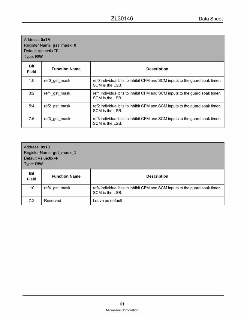
ZL30146 Data Sheet
Address: 0x1ARegister Name: gst_mask_0Default Value:0xFFType: R/W
Bit Field
Function Name Description
1:0 ref0_gst_mask ref0 individual bits to inhibit CFM and SCM inputs to the guard soak timer. SCM is the LSB.
3:2 ref1_gst_mask ref1 individual bits to inhibit CFM and SCM inputs to the guard soak timer. SCM is the LSB.
5:4 ref2_gst_mask ref2 individual bits to inhibit CFM and SCM inputs to the guard soak timer. SCM is the LSB.
7:6 ref3_gst_mask ref3 individual bits to inhibit CFM and SCM inputs to the guard soak timer. SCM is the LSB.
Address: 0x1BRegister Name: gst_mask_1Default Value:0xFFType: R/W
Bit Field
Function Name Description
1:0 ref4_gst_mask ref4 individual bits to inhibit CFM and SCM inputs to the guard soak timer. SCM is the LSB.
7:2 Reserved Leave as default
61Microsemi Corporation
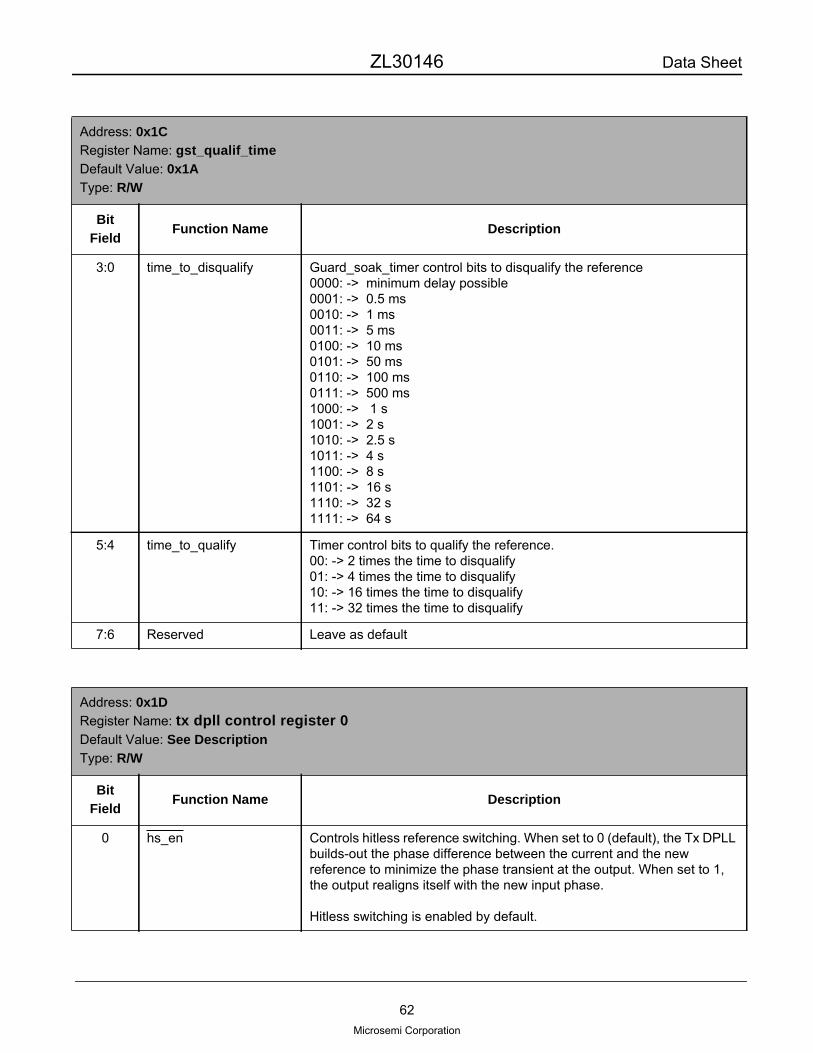
ZL30146 Data Sheet
Address: 0x1CRegister Name: gst_qualif_timeDefault Value: 0x1AType: R/W
Bit Field
Function Name Description
3:0 time_to_disqualify Guard_soak_timer control bits to disqualify the reference 0000: -> minimum delay possible0001: -> 0.5 ms0010: -> 1 ms0011: -> 5 ms0100: -> 10 ms0101: -> 50 ms0110: -> 100 ms0111: -> 500 ms1000: -> 1 s1001: -> 2 s1010: -> 2.5 s1011: -> 4 s1100: -> 8 s1101: -> 16 s1110: -> 32 s1111: -> 64 s
5:4 time_to_qualify Timer control bits to qualify the reference.00: -> 2 times the time to disqualify01: -> 4 times the time to disqualify10: -> 16 times the time to disqualify11: -> 32 times the time to disqualify
7:6 Reserved Leave as default
Address: 0x1DRegister Name: tx dpll control register 0Default Value: See DescriptionType: R/W
Bit Field
Function Name Description
0 hs_en Controls hitless reference switching. When set to 0 (default), the Tx DPLL builds-out the phase difference between the current and the new reference to minimize the phase transient at the output. When set to 1, the output realigns itself with the new input phase.
Hitless switching is enabled by default.
62Microsemi Corporation
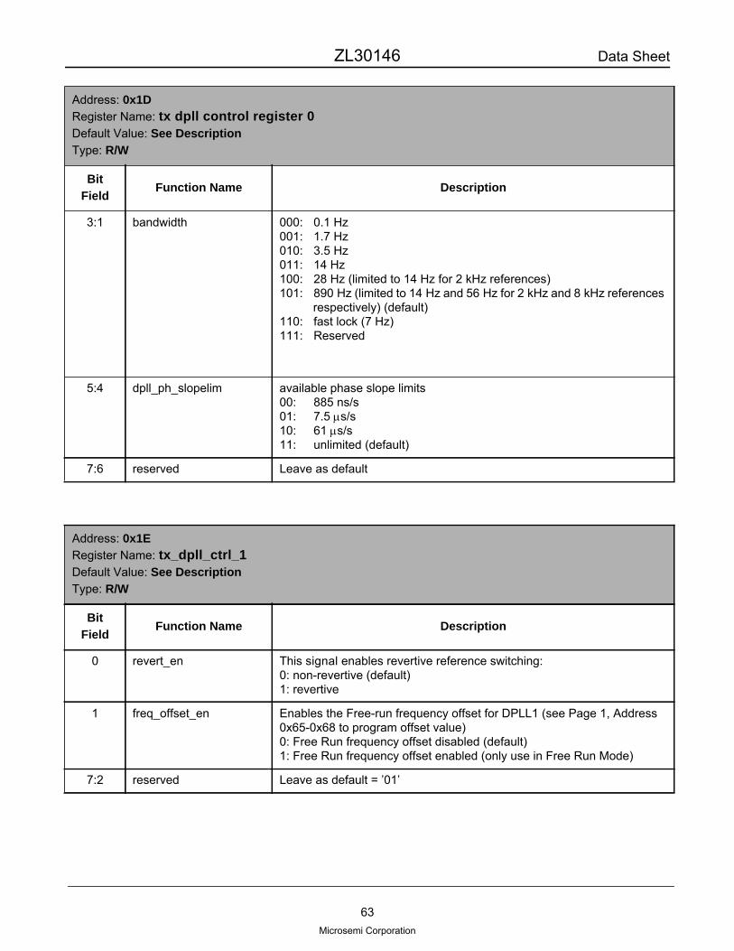
ZL30146 Data Sheet
3:1 bandwidth 000: 0.1 Hz001: 1.7 Hz010: 3.5 Hz011: 14 Hz100: 28 Hz (limited to 14 Hz for 2 kHz references)101: 890 Hz (limited to 14 Hz and 56 Hz for 2 kHz and 8 kHz references
respectively) (default)110: fast lock (7 Hz)111: Reserved
5:4 dpll_ph_slopelim available phase slope limits00: 885 ns/s01: 7.5 s/s10: 61 s/s11: unlimited (default)
7:6 reserved Leave as default
Address: 0x1ERegister Name: tx_dpll_ctrl_1Default Value: See DescriptionType: R/W
Bit Field
Function Name Description
0 revert_en This signal enables revertive reference switching:0: non-revertive (default)1: revertive
1 freq_offset_en Enables the Free-run frequency offset for DPLL1 (see Page 1, Address 0x65-0x68 to program offset value)0: Free Run frequency offset disabled (default)1: Free Run frequency offset enabled (only use in Free Run Mode)
7:2 reserved Leave as default = ’01’
Address: 0x1DRegister Name: tx dpll control register 0Default Value: See DescriptionType: R/W
Bit Field
Function Name Description
63Microsemi Corporation
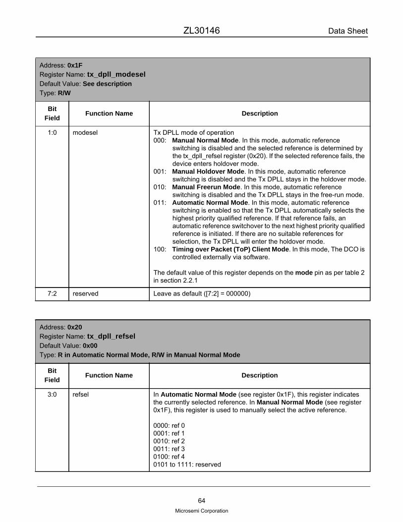
ZL30146 Data Sheet
Address: 0x1FRegister Name: tx_dpll_modeselDefault Value: See descriptionType: R/W
Bit Field
Function Name Description
1:0 modesel Tx DPLL mode of operation000: Manual Normal Mode. In this mode, automatic reference
switching is disabled and the selected reference is determined by the tx_dpll_refsel register (0x20). If the selected reference fails, the device enters holdover mode.
001: Manual Holdover Mode. In this mode, automatic reference switching is disabled and the Tx DPLL stays in the holdover mode.
010: Manual Freerun Mode. In this mode, automatic reference switching is disabled and the Tx DPLL stays in the free-run mode.
011: Automatic Normal Mode. In this mode, automatic reference switching is enabled so that the Tx DPLL automatically selects the highest priority qualified reference. If that reference fails, an automatic reference switchover to the next highest priority qualified reference is initiated. If there are no suitable references for selection, the Tx DPLL will enter the holdover mode.
100: Timing over Packet (ToP) Client Mode. In this mode, The DCO is controlled externally via software.
The default value of this register depends on the mode pin as per table 2 in section 2.2.1
7:2 reserved Leave as default ([7:2] = 000000)
Address: 0x20Register Name: tx_dpll_refselDefault Value: 0x00Type: R in Automatic Normal Mode, R/W in Manual Normal Mode
Bit Field
Function Name Description
3:0 refsel In Automatic Normal Mode (see register 0x1F), this register indicates the currently selected reference. In Manual Normal Mode (see register 0x1F), this register is used to manually select the active reference.
0000: ref 00001: ref 10010: ref 20011: ref 30100: ref 40101 to 1111: reserved
64Microsemi Corporation
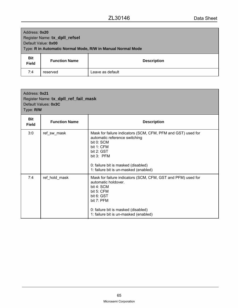
ZL30146 Data Sheet
7:4 reserved Leave as default
Address: 0x21Register Name: tx_dpll_ref_fail_maskDefault Values: 0x3CType: R/W
Bit Field
Function Name Description
3:0 ref_sw_mask Mask for failure indicators (SCM, CFM, PFM and GST) used for automatic reference switchingbit 0: SCMbit 1: CFMbit 2: GST bit 3: PFM
0: failure bit is masked (disabled)1: failure bit is un-masked (enabled)
7:4 ref_hold_mask Mask for failure indicators (SCM, CFM, GST and PFM) used for automatic holdover.bit 4: SCMbit 5: CFMbit 6: GST bit 7: PFM
0: failure bit is masked (disabled)1: failure bit is un-masked (enabled)
Address: 0x20Register Name: tx_dpll_refselDefault Value: 0x00Type: R in Automatic Normal Mode, R/W in Manual Normal Mode
Bit Field
Function Name Description
65Microsemi Corporation
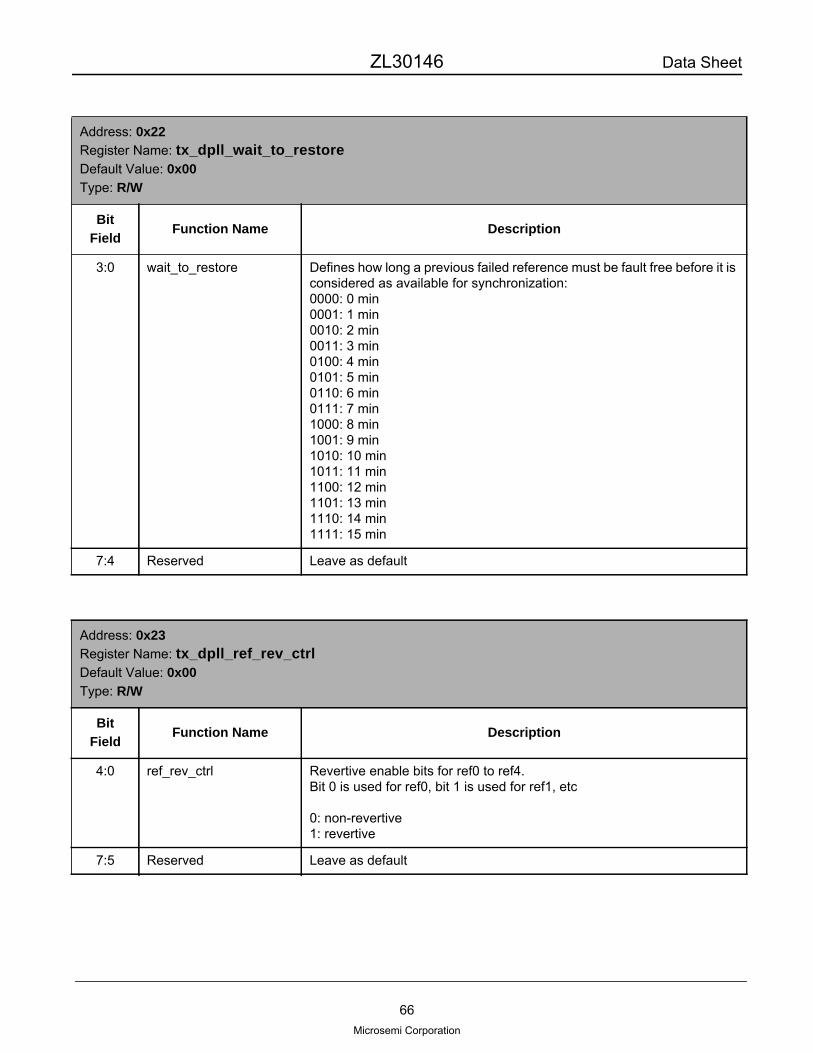
ZL30146 Data Sheet
Address: 0x22Register Name: tx_dpll_wait_to_restoreDefault Value: 0x00Type: R/W
Bit Field
Function Name Description
3:0 wait_to_restore Defines how long a previous failed reference must be fault free before it is considered as available for synchronization:0000: 0 min0001: 1 min0010: 2 min0011: 3 min0100: 4 min0101: 5 min0110: 6 min0111: 7 min1000: 8 min1001: 9 min1010: 10 min1011: 11 min1100: 12 min1101: 13 min1110: 14 min1111: 15 min
7:4 Reserved Leave as default
Address: 0x23Register Name: tx_dpll_ref_rev_ctrlDefault Value: 0x00Type: R/W
Bit Field
Function Name Description
4:0 ref_rev_ctrl Revertive enable bits for ref0 to ref4. Bit 0 is used for ref0, bit 1 is used for ref1, etc
0: non-revertive1: revertive
7:5 Reserved Leave as default
66Microsemi Corporation
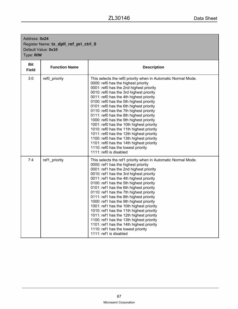
ZL30146 Data Sheet
Address: 0x24Register Name: tx_dpll_ref_pri_ctrl_0Default Value: 0x10Type: R/W
Bit Field
Function Name Description
3:0 ref0_priority This selects the ref0 priority when in Automatic Normal Mode. 0000: ref0 has the highest priority 0001: ref0 has the 2nd highest priority0010: ref0 has the 3rd highest priority0011: ref0 has the 4th highest priority0100: ref0 has the 5th highest priority0101: ref0 has the 6th highest priority0110: ref0 has the 7th highest priority0111: ref0 has the 8th highest priority1000: ref0 has the 9th highest priority1001: ref0 has the 10th highest priority1010: ref0 has the 11th highest priority1011: ref0 has the 12th highest priority1100: ref0 has the 13th highest priority1101: ref0 has the 14th highest priority1110: ref0 has the lowest priority1111: ref0 is disabled
7:4 ref1_priority This selects the ref1 priority when in Automatic Normal Mode. 0000: ref1 has the highest priority 0001: ref1 has the 2nd highest priority0010: ref1 has the 3rd highest priority0011: ref1 has the 4th highest priority0100: ref1 has the 5th highest priority0101: ref1 has the 6th highest priority0110: ref1 has the 7th highest priority0111: ref1 has the 8th highest priority1000: ref1 has the 9th highest priority1001: ref1 has the 10th highest priority1010: ref1 has the 11th highest priority1011: ref1 has the 12th highest priority1100: ref1 has the 13th highest priority1101: ref1 has the 14th highest priority1110: ref1 has the lowest priority1111: ref1 is disabled
67Microsemi Corporation
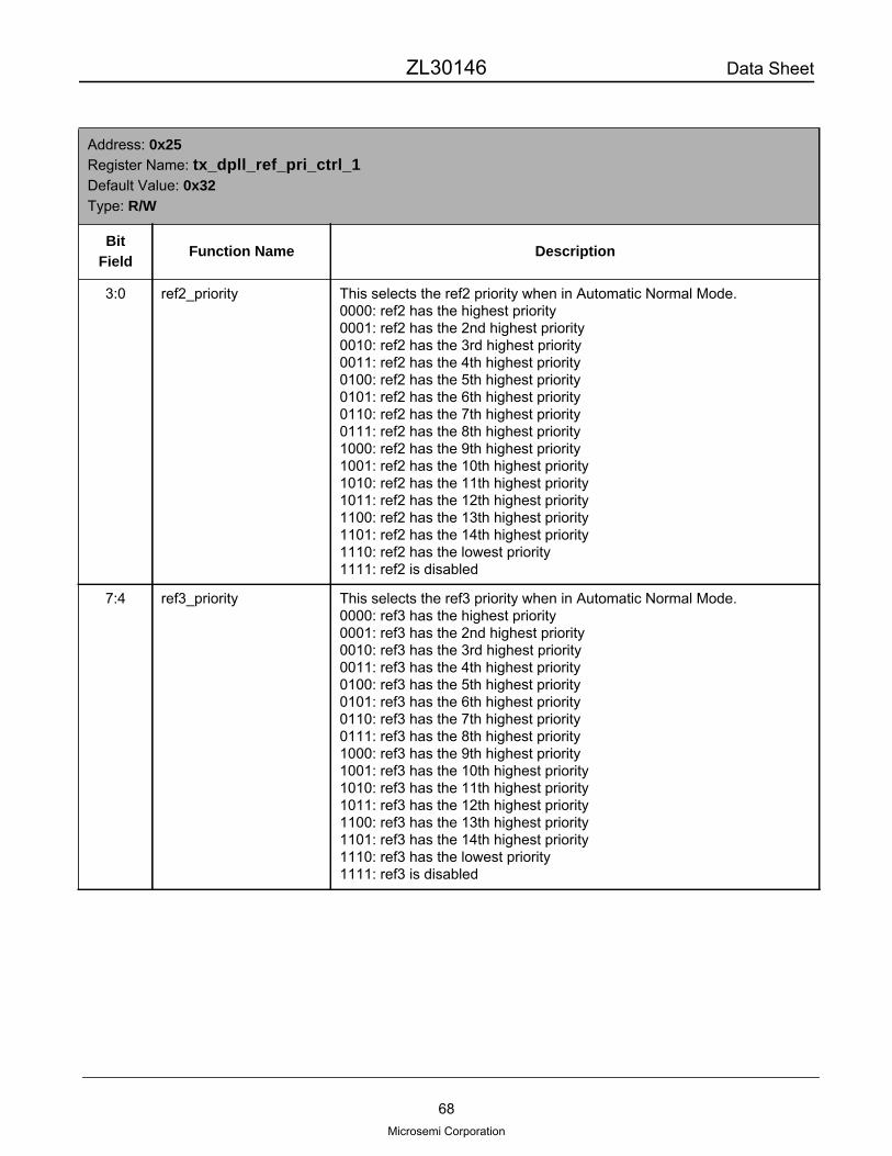
ZL30146 Data Sheet
Address: 0x25Register Name: tx_dpll_ref_pri_ctrl_1Default Value: 0x32Type: R/W
Bit Field
Function Name Description
3:0 ref2_priority This selects the ref2 priority when in Automatic Normal Mode. 0000: ref2 has the highest priority 0001: ref2 has the 2nd highest priority0010: ref2 has the 3rd highest priority0011: ref2 has the 4th highest priority0100: ref2 has the 5th highest priority0101: ref2 has the 6th highest priority0110: ref2 has the 7th highest priority0111: ref2 has the 8th highest priority1000: ref2 has the 9th highest priority1001: ref2 has the 10th highest priority1010: ref2 has the 11th highest priority1011: ref2 has the 12th highest priority1100: ref2 has the 13th highest priority1101: ref2 has the 14th highest priority1110: ref2 has the lowest priority1111: ref2 is disabled
7:4 ref3_priority This selects the ref3 priority when in Automatic Normal Mode. 0000: ref3 has the highest priority 0001: ref3 has the 2nd highest priority0010: ref3 has the 3rd highest priority0011: ref3 has the 4th highest priority0100: ref3 has the 5th highest priority0101: ref3 has the 6th highest priority0110: ref3 has the 7th highest priority0111: ref3 has the 8th highest priority1000: ref3 has the 9th highest priority1001: ref3 has the 10th highest priority1010: ref3 has the 11th highest priority1011: ref3 has the 12th highest priority1100: ref3 has the 13th highest priority1101: ref3 has the 14th highest priority1110: ref3 has the lowest priority1111: ref3 is disabled
68Microsemi Corporation
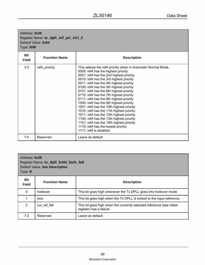
ZL30146 Data Sheet
Address: 0x26Register Name: tx_dpll_ref_pri_ctrl_2Default Value: 0x54Type: R/W
Bit Field
Function Name Description
3:0 ref4_priority This selects the ref4 priority when in Automatic Normal Mode. 0000: ref4 has the highest priority 0001: ref4 has the 2nd highest priority0010: ref4 has the 3rd highest priority0011: ref4 has the 4th highest priority0100: ref4 has the 5th highest priority0101: ref4 has the 6th highest priority0110: ref4 has the 7th highest priority0111: ref4 has the 8th highest priority1000: ref4 has the 9th highest priority1001: ref4 has the 10th highest priority1010: ref4 has the 11th highest priority1011: ref4 has the 12th highest priority1100: ref4 has the 13th highest priority1101: ref4 has the 14th highest priority1110: ref4 has the lowest priority1111: ref4 is disabled
7:4 Reserved Leave as default
Address: 0x28Register Name: tx_dpll_hold_lock_failDefault Value: See DescriptionType: R
Bit Field
Function Name Description
0 holdover This bit goes high whenever the Tx DPLL goes into holdover mode
1 lock This bit goes high when the Tx DPLL is locked to the input reference
2 cur_ref_fail This bit goes high when the currently selected reference (see refsel register) has a failure.
7:3 Reserved Leave as default
69Microsemi Corporation
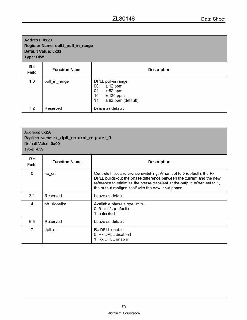
ZL30146 Data Sheet
Address: 0x29Register Name: dpll1_pull_in_rangeDefault Value: 0x03Type: R/W
Bit Field
Function Name Description
1:0 pull_in_range DPLL pull-in range00: ± 12 ppm01: ± 52 ppm 10: ± 130 ppm11: ± 83 ppm (default)
7:2 Reserved Leave as default
Address: 0x2ARegister Name: rx_dpll_control_register_0Default Value: 0x00Type: R/W
Bit Field
Function Name Description
0 hs_en Controls hitless reference switching. When set to 0 (default), the Rx DPLL builds-out the phase difference between the current and the new reference to minimize the phase transient at the output. When set to 1, the output realigns itself with the new input phase.
3:1 Reserved Leave as default
4 ph_slopelim Available phase slope limits0: 61 ms/s (default)1: unlimited
6:5 Reserved Leave as default
7 dpll_en Rx DPLL enable0: Rx DPLL disabled1: Rx DPLL enable
70Microsemi Corporation
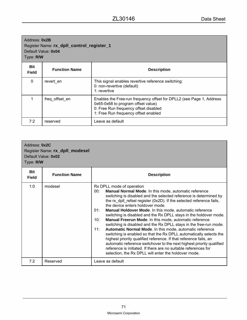
ZL30146 Data Sheet
Address: 0x2BRegister Name: rx_dpll_control_register_1Default Value: 0x04Type: R/W
Bit Field
Function Name Description
0 revert_en This signal enables revertive reference switching:0: non-revertive (default)1: revertive
1 freq_offset_en Enables the Free-run frequency offset for DPLL2 (see Page 1, Address 0x65-0x68 to program offset value)0: Free Run frequency offset disabled1: Free Run frequency offset enabled
7:2 reserved Leave as default
Address: 0x2CRegister Name: rx_dpll_modeselDefault Value: 0x02Type: R/W
Bit Field
Function Name Description
1:0 modesel Rx DPLL mode of operation00: Manual Normal Mode. In this mode, automatic reference
switching is disabled and the selected reference is determined by the rx_dpll_refsel register (0x2D). If the selected reference fails, the device enters holdover mode.
01: Manual Holdover Mode. In this mode, automatic reference switching is disabled and the Rx DPLL stays in the holdover mode.
10: Manual Freerun Mode. In this mode, automatic reference switching is disabled and the Rx DPLL stays in the free-run mode.
11: Automatic Normal Mode. In this mode, automatic reference switching is enabled so that the Rx DPLL automatically selects the highest priority qualified reference. If that reference fails, an automatic reference switchover to the next highest priority qualified reference is initiated. If there are no suitable references for selection, the Rx DPLL will enter the holdover mode.
7:2 Reserved Leave as default
71Microsemi Corporation
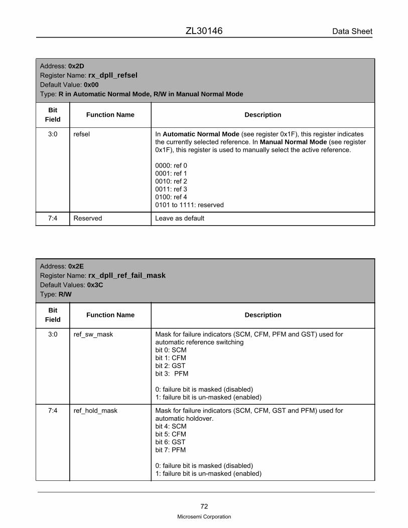
ZL30146 Data Sheet
Address: 0x2DRegister Name: rx_dpll_refselDefault Value: 0x00Type: R in Automatic Normal Mode, R/W in Manual Normal Mode
Bit Field
Function Name Description
3:0 refsel In Automatic Normal Mode (see register 0x1F), this register indicates the currently selected reference. In Manual Normal Mode (see register 0x1F), this register is used to manually select the active reference.
0000: ref 00001: ref 10010: ref 20011: ref 30100: ref 40101 to 1111: reserved
7:4 Reserved Leave as default
Address: 0x2ERegister Name: rx_dpll_ref_fail_maskDefault Values: 0x3CType: R/W
Bit Field
Function Name Description
3:0 ref_sw_mask Mask for failure indicators (SCM, CFM, PFM and GST) used for automatic reference switchingbit 0: SCMbit 1: CFMbit 2: GST bit 3: PFM
0: failure bit is masked (disabled)1: failure bit is un-masked (enabled)
7:4 ref_hold_mask Mask for failure indicators (SCM, CFM, GST and PFM) used for automatic holdover.bit 4: SCMbit 5: CFMbit 6: GST bit 7: PFM
0: failure bit is masked (disabled)1: failure bit is un-masked (enabled)
72Microsemi Corporation
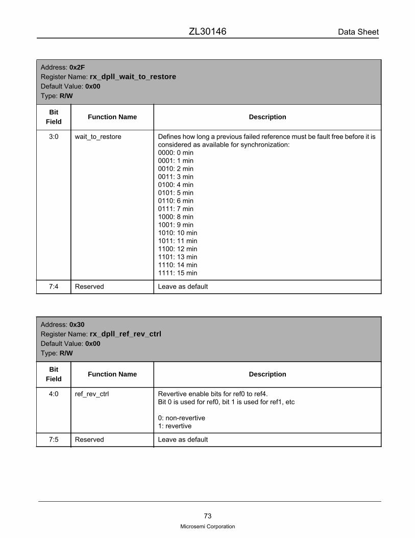
ZL30146 Data Sheet
Address: 0x2FRegister Name: rx_dpll_wait_to_restoreDefault Value: 0x00Type: R/W
Bit Field
Function Name Description
3:0 wait_to_restore Defines how long a previous failed reference must be fault free before it is considered as available for synchronization:0000: 0 min0001: 1 min0010: 2 min0011: 3 min0100: 4 min0101: 5 min0110: 6 min0111: 7 min1000: 8 min1001: 9 min1010: 10 min1011: 11 min1100: 12 min1101: 13 min1110: 14 min1111: 15 min
7:4 Reserved Leave as default
Address: 0x30Register Name: rx_dpll_ref_rev_ctrlDefault Value: 0x00Type: R/W
Bit Field
Function Name Description
4:0 ref_rev_ctrl Revertive enable bits for ref0 to ref4. Bit 0 is used for ref0, bit 1 is used for ref1, etc
0: non-revertive1: revertive
7:5 Reserved Leave as default
73Microsemi Corporation

ZL30146 Data Sheet
Address: 0x31Register Name: rx_dpll_ref_pri_ctrl_0Default Value: 0x10Type: R/W
Bit Field
Function Name Description
3:0 ref0_priority This selects the ref0 priority when in Automatic Normal Mode. 0000: ref0 has the highest priority 0001: ref0 has the 2nd highest priority0010: ref0 has the 3rd highest priority0011: ref0 has the 4th highest priority0100: ref0 has the 5th highest priority0101: ref0 has the 6th highest priority0110: ref0 has the 7th highest priority0111: ref0 has the 8th highest priority1000: ref0 has the 9th highest priority1001: ref0 has the 10th highest priority1010: ref0 has the 11th highest priority1011: ref0 has the 12th highest priority1100: ref0 has the 13th highest priority1101: ref0 has the 14th highest priority1110: ref0 has the lowest priority1111: ref0 is disabled
7:4 ref1_priority This selects the ref1 priority when in Automatic Normal Mode. 0000: ref1 has the highest priority 0001: ref1 has the 2nd highest priority0010: ref1 has the 3rd highest priority0011: ref1 has the 4th highest priority0100: ref1 has the 5th highest priority0101: ref1 has the 6th highest priority0110: ref1 has the 7th highest priority0111: ref1 has the 8th highest priority1000: ref1 has the 9th highest priority1001: ref1 has the 10th highest priority1010: ref1 has the 11th highest priority1011: ref1 has the 12th highest priority1100: ref1 has the 13th highest priority1101: ref1 has the 14th highest priority1110: ref1 has the lowest priority1111: ref1 is disabled
74Microsemi Corporation

ZL30146 Data Sheet
Address: 0x32Register Name: rx_dpll_ref_pri_ctrl_1Default Value: 0x32Type: R/W
Bit Field
Function Name Description
3:0 ref2_priority This selects the ref2 priority when in Automatic Normal Mode. 0000: ref2 has the highest priority 0001: ref2 has the 2nd highest priority0010: ref2 has the 3rd highest priority0011: ref2 has the 4th highest priority0100: ref2 has the 5th highest priority0101: ref2 has the 6th highest priority0110: ref2 has the 7th highest priority0111: ref2 has the 8th highest priority1000: ref2 has the 9th highest priority1001: ref2 has the 10th highest priority1010: ref2 has the 11th highest priority1011: ref2 has the 12th highest priority1100: ref2 has the 13th highest priority1101: ref2 has the 14th highest priority1110: ref2 has the lowest priority1111: ref2 is disabled
7:4 ref3_priority This selects the ref3 priority when in Automatic Normal Mode. 0000: ref3 has the highest priority 0001: ref3 has the 2nd highest priority0010: ref3 has the 3rd highest priority0011: ref3 has the 4th highest priority0100: ref3 has the 5th highest priority0101: ref3 has the 6th highest priority0110: ref3 has the 7th highest priority0111: ref3 has the 8th highest priority1000: ref3 has the 9th highest priority1001: ref3 has the 10th highest priority1010: ref3 has the 11th highest priority1011: ref3 has the 12th highest priority1100: ref3 has the 13th highest priority1101: ref3 has the 14th highest priority1110: ref3 has the lowest priority1111: ref3 is disabled
75Microsemi Corporation
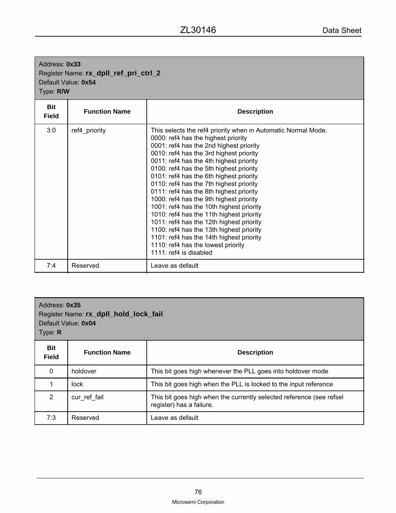
ZL30146 Data Sheet
Address: 0x33Register Name: rx_dpll_ref_pri_ctrl_2Default Value: 0x54Type: R/W
Bit Field
Function Name Description
3:0 ref4_priority This selects the ref4 priority when in Automatic Normal Mode. 0000: ref4 has the highest priority 0001: ref4 has the 2nd highest priority0010: ref4 has the 3rd highest priority0011: ref4 has the 4th highest priority0100: ref4 has the 5th highest priority0101: ref4 has the 6th highest priority0110: ref4 has the 7th highest priority0111: ref4 has the 8th highest priority1000: ref4 has the 9th highest priority1001: ref4 has the 10th highest priority1010: ref4 has the 11th highest priority1011: ref4 has the 12th highest priority1100: ref4 has the 13th highest priority1101: ref4 has the 14th highest priority1110: ref4 has the lowest priority1111: ref4 is disabled
7:4 Reserved Leave as default
Address: 0x35Register Name: rx_dpll_hold_lock_failDefault Value: 0x04Type: R
Bit Field
Function Name Description
0 holdover This bit goes high whenever the PLL goes into holdover mode
1 lock This bit goes high when the PLL is locked to the input reference
2 cur_ref_fail This bit goes high when the currently selected reference (see refsel register) has a failure.
7:3 Reserved Leave as default
76Microsemi Corporation
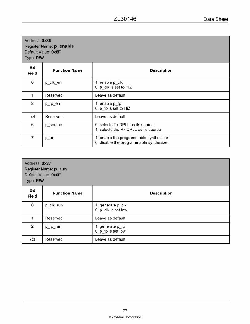
ZL30146 Data Sheet
Address: 0x36Register Name: p_enableDefault Value: 0x8FType: R/W
Bit Field
Function Name Description
0 p_clk_en 1: enable p_clk0: p_clk is set to HiZ
1 Reserved Leave as default
2 p_fp_en 1: enable p_fp0: p_fp is set to HiZ
5:4 Reserved Leave as default
6 p_source 0: selects Tx DPLL as its source1: selects the Rx DPLL as its source
7 p_en 1: enable the programmable synthesizer0: disable the programmable synthesizer
Address: 0x37Register Name: p_runDefault Value: 0x0FType: R/W
Bit Field
Function Name Description
0 p_clk_run 1: generate p_clk0: p_clk is set low
1 Reserved Leave as default
2 p_fp_run 1: generate p_fp0: p_fp is set low
7:3 Reserved Leave as default
77Microsemi Corporation
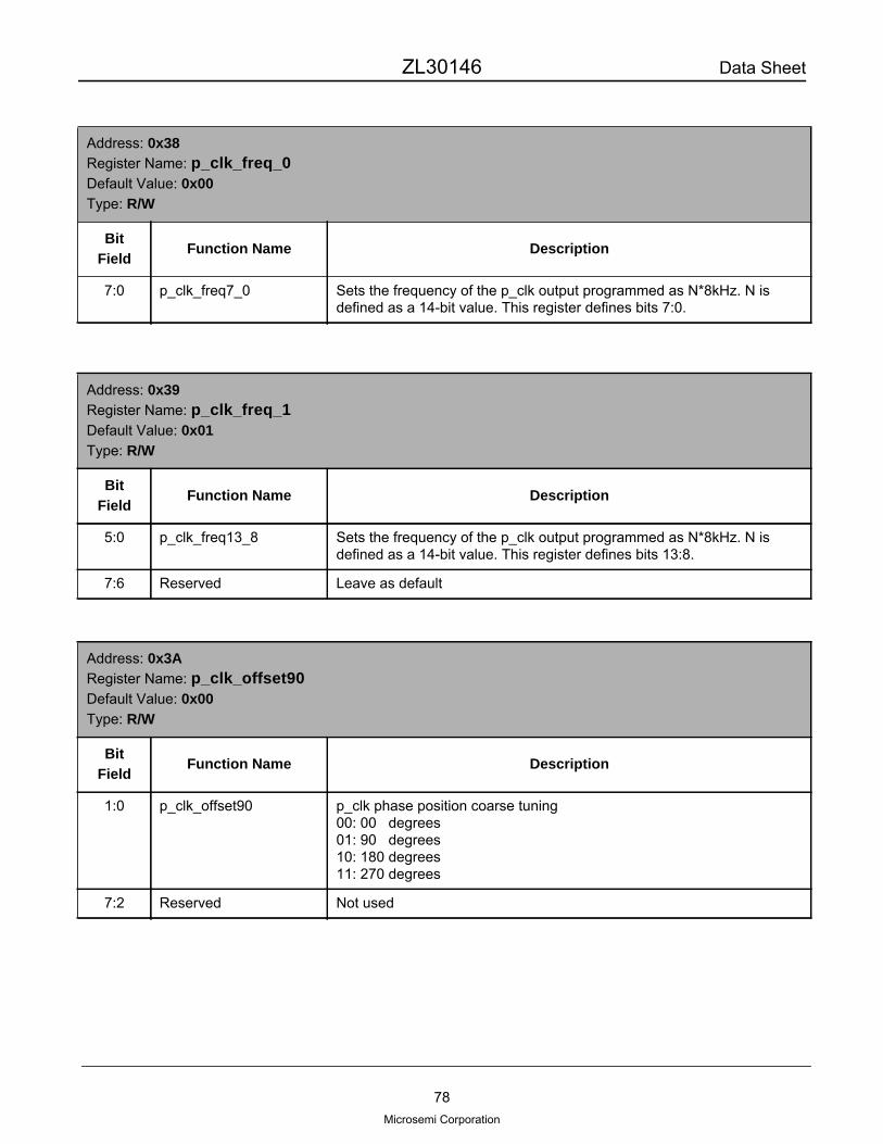
ZL30146 Data Sheet
Address: 0x38Register Name: p_clk_freq_0Default Value: 0x00Type: R/W
Bit Field
Function Name Description
7:0 p_clk_freq7_0 Sets the frequency of the p_clk output programmed as N*8kHz. N is defined as a 14-bit value. This register defines bits 7:0.
Address: 0x39Register Name: p_clk_freq_1Default Value: 0x01Type: R/W
Bit Field
Function Name Description
5:0 p_clk_freq13_8 Sets the frequency of the p_clk output programmed as N*8kHz. N is defined as a 14-bit value. This register defines bits 13:8.
7:6 Reserved Leave as default
Address: 0x3ARegister Name: p_clk_offset90Default Value: 0x00Type: R/W
Bit Field
Function Name Description
1:0 p_clk_offset90 p_clk phase position coarse tuning00: 00 degrees01: 90 degrees10: 180 degrees11: 270 degrees
7:2 Reserved Not used
78Microsemi Corporation
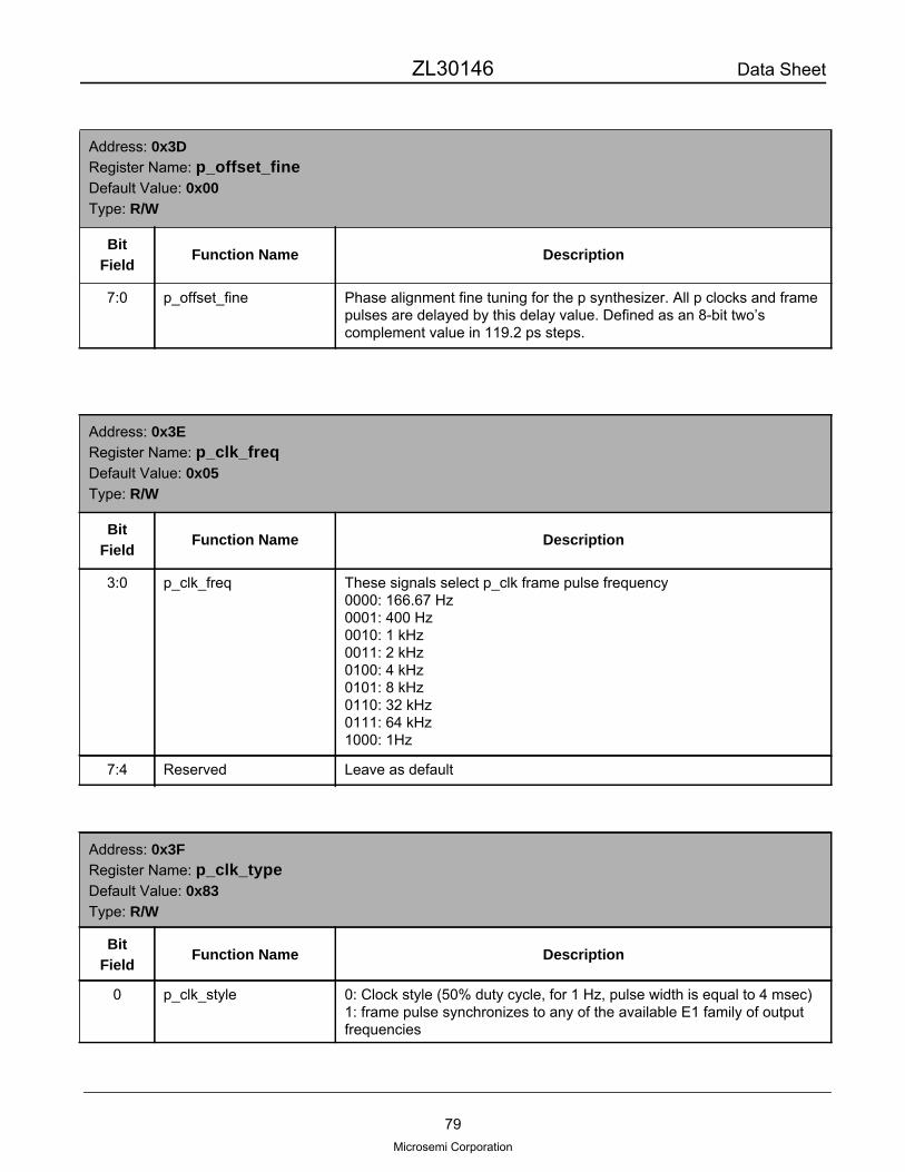
ZL30146 Data Sheet
Address: 0x3DRegister Name: p_offset_fineDefault Value: 0x00Type: R/W
Bit Field
Function Name Description
7:0 p_offset_fine Phase alignment fine tuning for the p synthesizer. All p clocks and frame pulses are delayed by this delay value. Defined as an 8-bit two’s complement value in 119.2 ps steps.
Address: 0x3ERegister Name: p_clk_freqDefault Value: 0x05Type: R/W
Bit Field
Function Name Description
3:0 p_clk_freq These signals select p_clk frame pulse frequency 0000: 166.67 Hz0001: 400 Hz0010: 1 kHz0011: 2 kHz0100: 4 kHz0101: 8 kHz0110: 32 kHz0111: 64 kHz1000: 1Hz
7:4 Reserved Leave as default
Address: 0x3FRegister Name: p_clk_typeDefault Value: 0x83Type: R/W
Bit Field
Function Name Description
0 p_clk_style 0: Clock style (50% duty cycle, for 1 Hz, pulse width is equal to 4 msec)1: frame pulse synchronizes to any of the available E1 family of output frequencies
79Microsemi Corporation
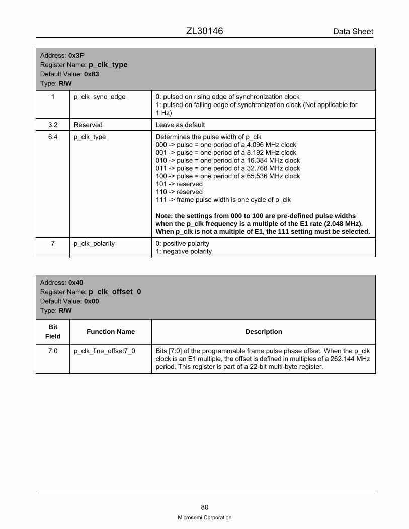
ZL30146 Data Sheet
1 p_clk_sync_edge 0: pulsed on rising edge of synchronization clock1: pulsed on falling edge of synchronization clock (Not applicable for 1 Hz)
3:2 Reserved Leave as default
6:4 p_clk_type Determines the pulse width of p_clk000 -> pulse = one period of a 4.096 MHz clock001 -> pulse = one period of a 8.192 MHz clock010 -> pulse = one period of a 16.384 MHz clock011 -> pulse = one period of a 32.768 MHz clock100 -> pulse = one period of a 65.536 MHz clock101 -> reserved110 -> reserved111 -> frame pulse width is one cycle of p_clk
Note: the settings from 000 to 100 are pre-defined pulse widths when the p_clk frequency is a multiple of the E1 rate (2.048 MHz). When p_clk is not a multiple of E1, the 111 setting must be selected.
7 p_clk_polarity 0: positive polarity1: negative polarity
Address: 0x40Register Name: p_clk_offset_0Default Value: 0x00Type: R/W
Bit Field
Function Name Description
7:0 p_clk_fine_offset7_0 Bits [7:0] of the programmable frame pulse phase offset. When the p_clk clock is an E1 multiple, the offset is defined in multiples of a 262.144 MHz period. This register is part of a 22-bit multi-byte register.
Address: 0x3FRegister Name: p_clk_typeDefault Value: 0x83Type: R/W
80Microsemi Corporation
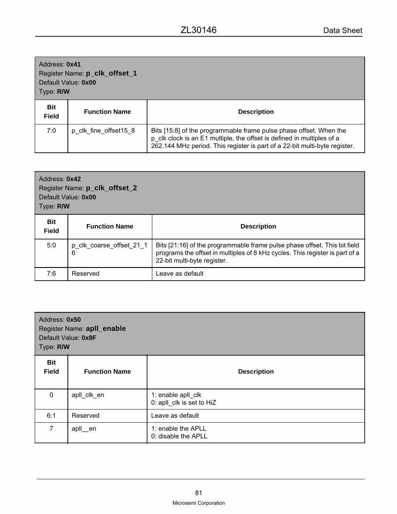
ZL30146 Data Sheet
Address: 0x41Register Name: p_clk_offset_1Default Value: 0x00Type: R/W
Bit Field
Function Name Description
7:0 p_clk_fine_offset15_8 Bits [15:8] of the programmable frame pulse phase offset. When the p_clk clock is an E1 multiple, the offset is defined in multiples of a 262.144 MHz period. This register is part of a 22-bit multi-byte register.
Address: 0x42Register Name: p_clk_offset_2Default Value: 0x00Type: R/W
Bit Field
Function Name Description
5:0 p_clk_coarse_offset_21_16
Bits [21:16] of the programmable frame pulse phase offset. This bit field programs the offset in multiples of 8 kHz cycles. This register is part of a 22-bit multi-byte register.
7:6 Reserved Leave as default
Address: 0x50Register Name: apll_enableDefault Value: 0x8FType: R/W
Bit Field Function Name Description
0 apll_clk_en 1: enable apll_clk0: apll_clk is set to HiZ
6:1 Reserved Leave as default
7 apll__en 1: enable the APLL0: disable the APLL
81Microsemi Corporation
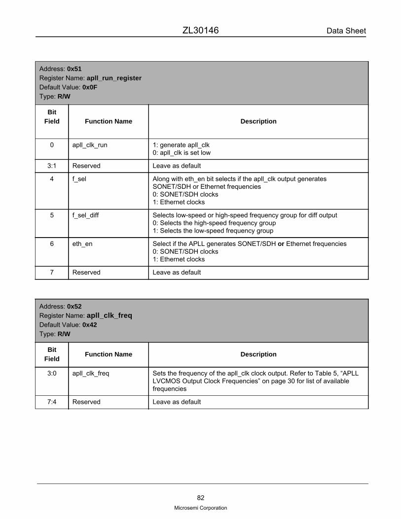
ZL30146 Data Sheet
Address: 0x51Register Name: apll_run_registerDefault Value: 0x0FType: R/W
Bit Field Function Name Description
0 apll_clk_run 1: generate apll_clk0: apll_clk is set low
3:1 Reserved Leave as default
4 f_sel Along with eth_en bit selects if the apll_clk output generatesSONET/SDH or Ethernet frequencies0: SONET/SDH clocks1: Ethernet clocks
5 f_sel_diff Selects low-speed or high-speed frequency group for diff output0: Selects the high-speed frequency group1: Selects the low-speed frequency group
6 eth_en Select if the APLL generates SONET/SDH or Ethernet frequencies0: SONET/SDH clocks1: Ethernet clocks
7 Reserved Leave as default
Address: 0x52Register Name: apll_clk_freqDefault Value: 0x42Type: R/W
Bit Field
Function Name Description
3:0 apll_clk_freq Sets the frequency of the apll_clk clock output. Refer to Table 5, “APLL LVCMOS Output Clock Frequencies” on page 30 for list of available frequencies
7:4 Reserved Leave as default
82Microsemi Corporation
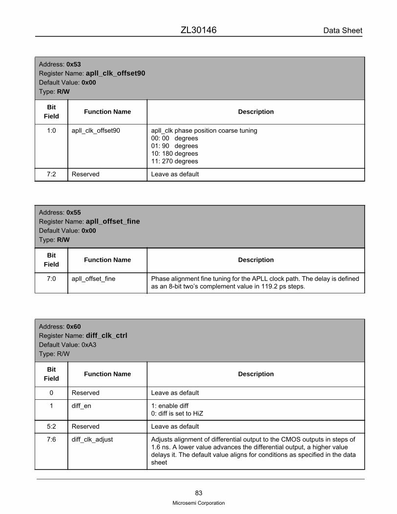
ZL30146 Data Sheet
Address: 0x53Register Name: apll_clk_offset90Default Value: 0x00Type: R/W
Bit Field
Function Name Description
1:0 apll_clk_offset90 apll_clk phase position coarse tuning00: 00 degrees01: 90 degrees10: 180 degrees11: 270 degrees
7:2 Reserved Leave as default
Address: 0x55Register Name: apll_offset_fineDefault Value: 0x00Type: R/W
Bit Field
Function Name Description
7:0 apll_offset_fine Phase alignment fine tuning for the APLL clock path. The delay is defined as an 8-bit two’s complement value in 119.2 ps steps.
Address: 0x60Register Name: diff_clk_ctrlDefault Value: 0xA3Type: R/W
Bit Field
Function Name Description
0 Reserved Leave as default
1 diff_en 1: enable diff0: diff is set to HiZ
5:2 Reserved Leave as default
7:6 diff_clk_adjust Adjusts alignment of differential output to the CMOS outputs in steps of 1.6 ns. A lower value advances the differential output, a higher value delays it. The default value aligns for conditions as specified in the data sheet
83Microsemi Corporation
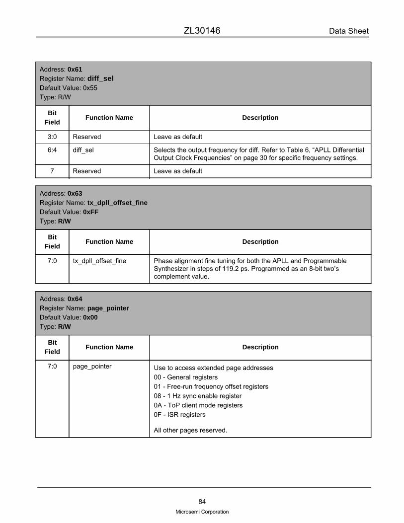
ZL30146 Data Sheet
Address: 0x61Register Name: diff_selDefault Value: 0x55Type: R/W
Bit Field
Function Name Description
3:0 Reserved Leave as default
6:4 diff_sel Selects the output frequency for diff. Refer to Table 6, “APLL Differential Output Clock Frequencies” on page 30 for specific frequency settings.
7 Reserved Leave as default
Address: 0x63Register Name: tx_dpll_offset_fineDefault Value: 0xFFType: R/W
Bit Field
Function Name Description
7:0 tx_dpll_offset_fine Phase alignment fine tuning for both the APLL and Programmable Synthesizer in steps of 119.2 ps. Programmed as an 8-bit two’s complement value.
Address: 0x64Register Name: page_pointerDefault Value: 0x00Type: R/W
Bit Field
Function Name Description
7:0 page_pointer Use to access extended page addresses00 - General registers01 - Free-run frequency offset registers08 - 1 Hz sync enable register0A - ToP client mode registers0F - ISR registers
All other pages reserved.
84Microsemi Corporation
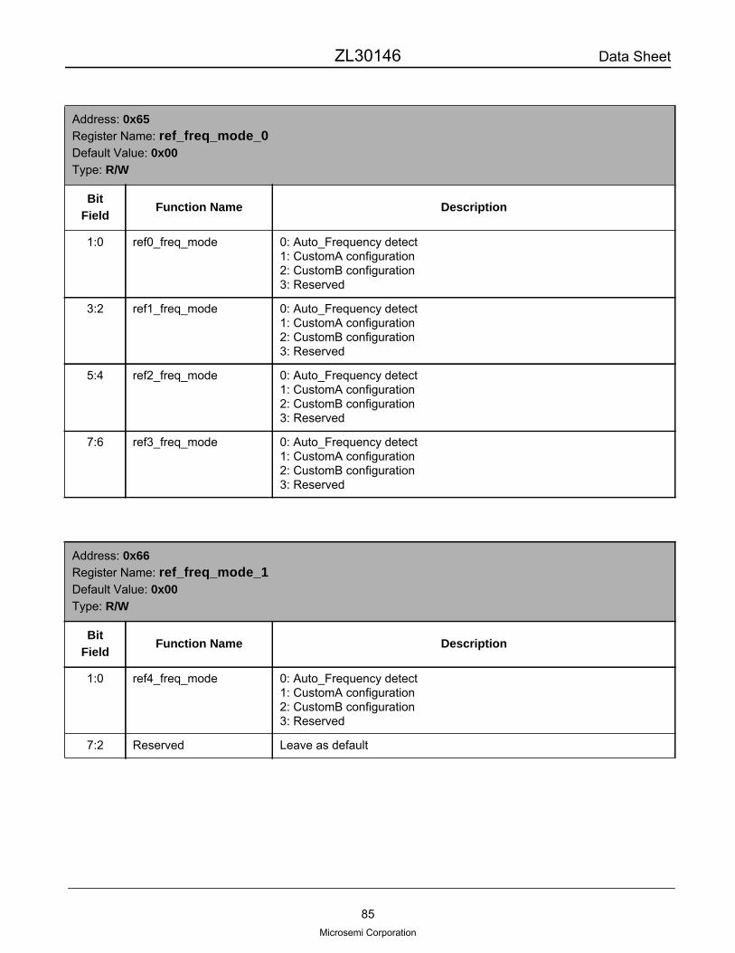
ZL30146 Data Sheet
Address: 0x65Register Name: ref_freq_mode_0Default Value: 0x00Type: R/W
Bit Field
Function Name Description
1:0 ref0_freq_mode 0: Auto_Frequency detect1: CustomA configuration2: CustomB configuration3: Reserved
3:2 ref1_freq_mode 0: Auto_Frequency detect1: CustomA configuration2: CustomB configuration3: Reserved
5:4 ref2_freq_mode 0: Auto_Frequency detect1: CustomA configuration2: CustomB configuration3: Reserved
7:6 ref3_freq_mode 0: Auto_Frequency detect1: CustomA configuration2: CustomB configuration3: Reserved
Address: 0x66Register Name: ref_freq_mode_1Default Value: 0x00Type: R/W
Bit Field
Function Name Description
1:0 ref4_freq_mode 0: Auto_Frequency detect1: CustomA configuration2: CustomB configuration3: Reserved
7:2 Reserved Leave as default
85Microsemi Corporation
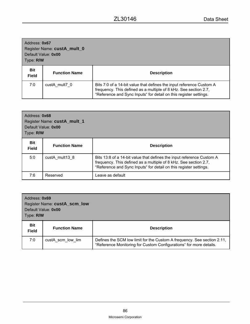
ZL30146 Data Sheet
Address: 0x67Register Name: custA_mult_0Default Value: 0x00Type: R/W
Bit Field
Function Name Description
7:0 custA_mult7_0 Bits 7:0 of a 14-bit value that defines the input reference Custom A frequency. This defined as a multiple of 8 kHz. See section 2.7, “Reference and Sync Inputs“ for detail on this register settings.
Address: 0x68Register Name: custA_mult_1Default Value: 0x00Type: R/W
Bit Field
Function Name Description
5:0 custA_mult13_8 Bits 13:8 of a 14-bit value that defines the input reference Custom A frequency. This defined as a multiple of 8 kHz. See section 2.7, “Reference and Sync Inputs“ for detail on this register settings.
7:6 Reserved Leave as default
Address: 0x69Register Name: custA_scm_lowDefault Value: 0x00Type: R/W
Bit Field
Function Name Description
7:0 custA_scm_low_lim Defines the SCM low limit for the Custom A frequency. See section 2.11, “Reference Monitoring for Custom Configurations“ for more details.
86Microsemi Corporation
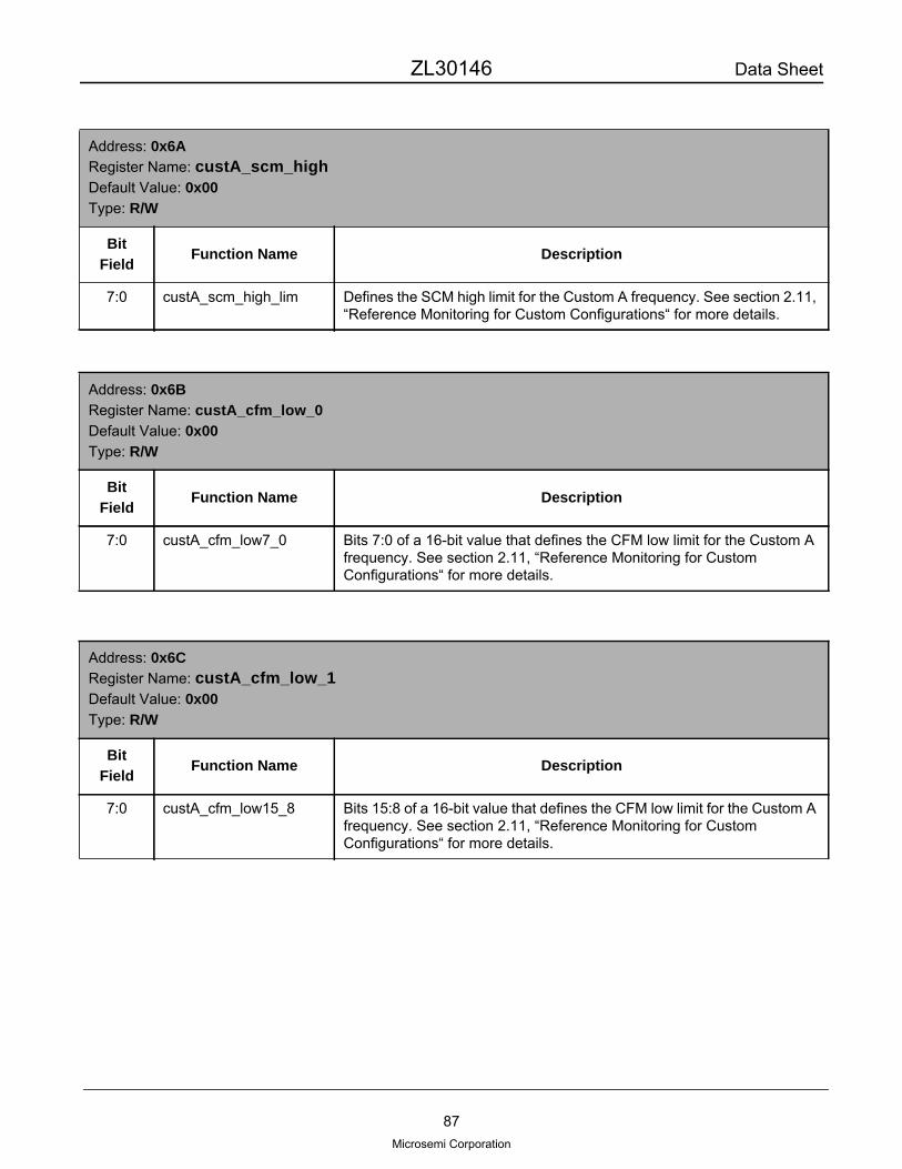
ZL30146 Data Sheet
Address: 0x6ARegister Name: custA_scm_highDefault Value: 0x00Type: R/W
Bit Field
Function Name Description
7:0 custA_scm_high_lim Defines the SCM high limit for the Custom A frequency. See section 2.11, “Reference Monitoring for Custom Configurations“ for more details.
Address: 0x6BRegister Name: custA_cfm_low_0Default Value: 0x00Type: R/W
Bit Field
Function Name Description
7:0 custA_cfm_low7_0 Bits 7:0 of a 16-bit value that defines the CFM low limit for the Custom A frequency. See section 2.11, “Reference Monitoring for Custom Configurations“ for more details.
Address: 0x6CRegister Name: custA_cfm_low_1Default Value: 0x00Type: R/W
Bit Field
Function Name Description
7:0 custA_cfm_low15_8 Bits 15:8 of a 16-bit value that defines the CFM low limit for the Custom A frequency. See section 2.11, “Reference Monitoring for Custom Configurations“ for more details.
87Microsemi Corporation
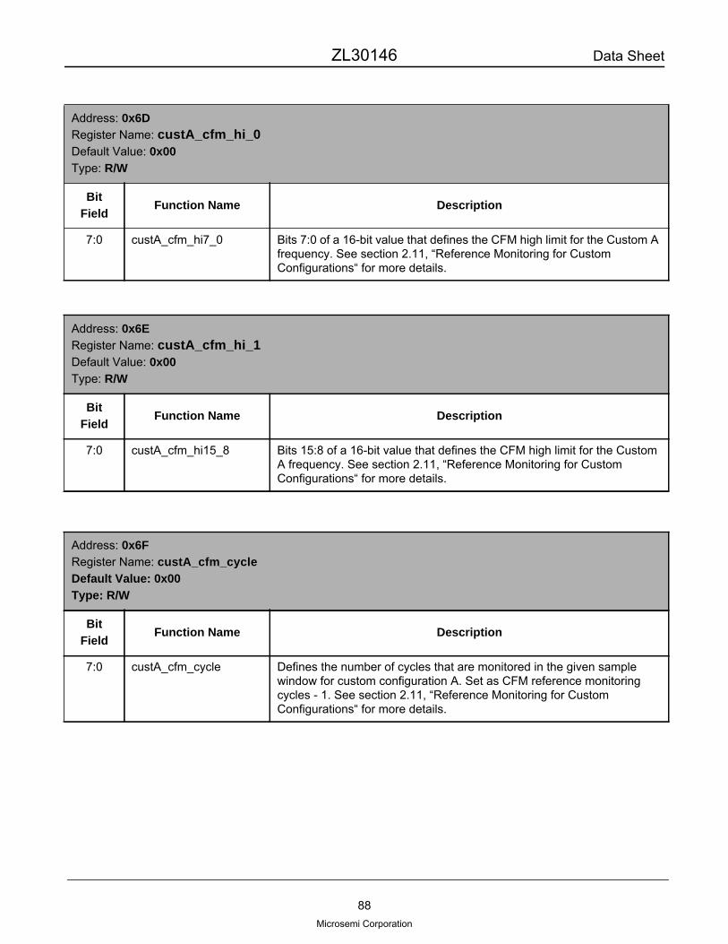
ZL30146 Data Sheet
Address: 0x6DRegister Name: custA_cfm_hi_0Default Value: 0x00Type: R/W
Bit Field
Function Name Description
7:0 custA_cfm_hi7_0 Bits 7:0 of a 16-bit value that defines the CFM high limit for the Custom A frequency. See section 2.11, “Reference Monitoring for Custom Configurations“ for more details.
Address: 0x6ERegister Name: custA_cfm_hi_1Default Value: 0x00Type: R/W
Bit Field
Function Name Description
7:0 custA_cfm_hi15_8 Bits 15:8 of a 16-bit value that defines the CFM high limit for the Custom A frequency. See section 2.11, “Reference Monitoring for Custom Configurations“ for more details.
Address: 0x6FRegister Name: custA_cfm_cycleDefault Value: 0x00Type: R/W
Bit Field
Function Name Description
7:0 custA_cfm_cycle Defines the number of cycles that are monitored in the given sample window for custom configuration A. Set as CFM reference monitoring cycles - 1. See section 2.11, “Reference Monitoring for Custom Configurations“ for more details.
88Microsemi Corporation
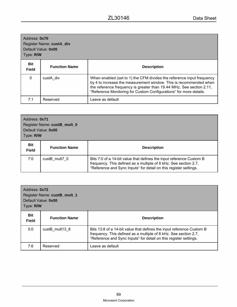
ZL30146 Data Sheet
Address: 0x70Register Name: custA_divDefault Value: 0x00Type: R/W
Bit Field
Function Name Description
0 custA_div When enabled (set to 1) the CFM divides the reference input frequency by 4 to increase the measurement window. This is recommended when the reference frequency is greater than 19.44 MHz. See section 2.11, “Reference Monitoring for Custom Configurations“ for more details.
7:1 Reserved Leave as default
Address: 0x71Register Name: custB_mult_0Default Value: 0x00Type: R/W
Bit Field
Function Name Description
7:0 custB_mult7_0 Bits 7:0 of a 14-bit value that defines the input reference Custom B frequency. This defined as a multiple of 8 kHz. See section 2.7, “Reference and Sync Inputs“ for detail on this register settings.
Address: 0x72Register Name: custB_mult_1Default Value: 0x00Type: R/W
Bit Field
Function Name Description
5:0 custB_mult13_8 Bits 13:8 of a 14-bit value that defines the input reference Custom B frequency. This defined as a multiple of 8 kHz. See section 2.7, “Reference and Sync Inputs“ for detail on this register settings.
7:6 Reserved Leave as default
89Microsemi Corporation
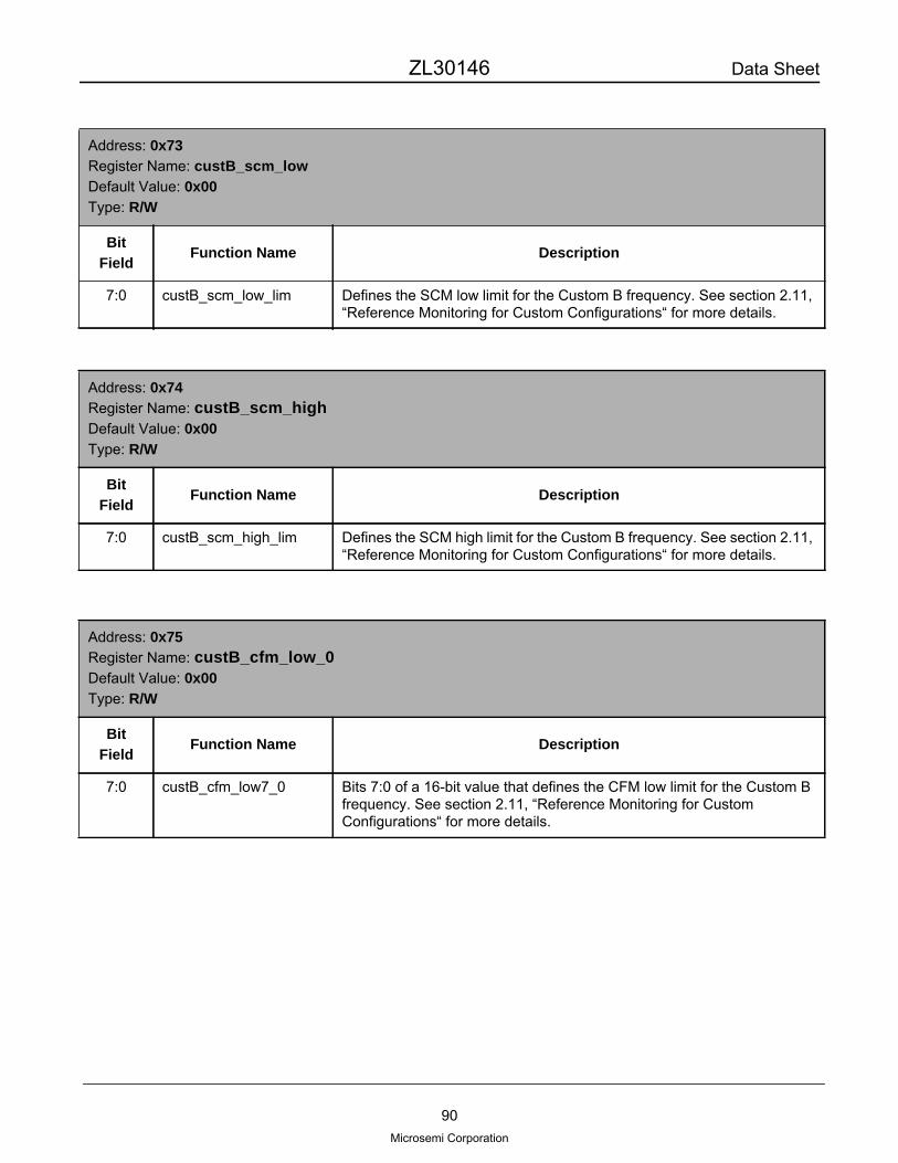
ZL30146 Data Sheet
Address: 0x73Register Name: custB_scm_lowDefault Value: 0x00Type: R/W
Bit Field
Function Name Description
7:0 custB_scm_low_lim Defines the SCM low limit for the Custom B frequency. See section 2.11, “Reference Monitoring for Custom Configurations“ for more details.
Address: 0x74Register Name: custB_scm_highDefault Value: 0x00Type: R/W
Bit Field
Function Name Description
7:0 custB_scm_high_lim Defines the SCM high limit for the Custom B frequency. See section 2.11, “Reference Monitoring for Custom Configurations“ for more details.
Address: 0x75Register Name: custB_cfm_low_0Default Value: 0x00Type: R/W
Bit Field
Function Name Description
7:0 custB_cfm_low7_0 Bits 7:0 of a 16-bit value that defines the CFM low limit for the Custom B frequency. See section 2.11, “Reference Monitoring for Custom Configurations“ for more details.
90Microsemi Corporation
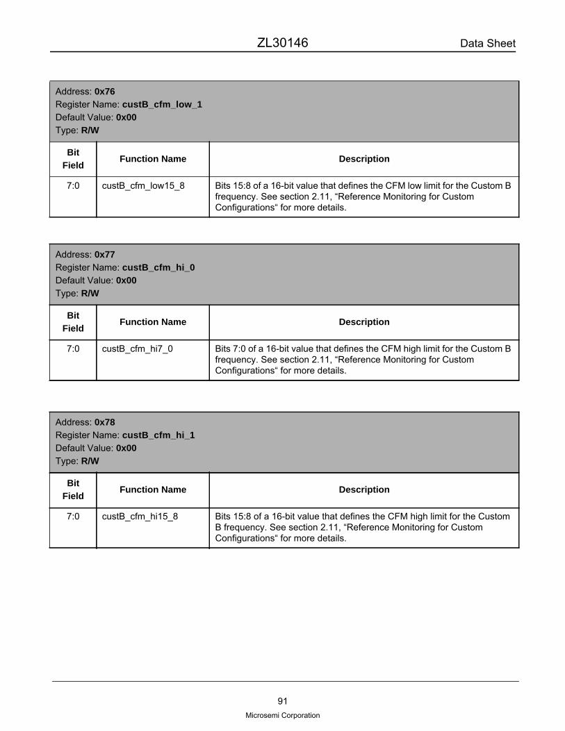
ZL30146 Data Sheet
Address: 0x76Register Name: custB_cfm_low_1Default Value: 0x00Type: R/W
Bit Field
Function Name Description
7:0 custB_cfm_low15_8 Bits 15:8 of a 16-bit value that defines the CFM low limit for the Custom B frequency. See section 2.11, “Reference Monitoring for Custom Configurations“ for more details.
Address: 0x77Register Name: custB_cfm_hi_0Default Value: 0x00Type: R/W
Bit Field
Function Name Description
7:0 custB_cfm_hi7_0 Bits 7:0 of a 16-bit value that defines the CFM high limit for the Custom B frequency. See section 2.11, “Reference Monitoring for Custom Configurations“ for more details.
Address: 0x78Register Name: custB_cfm_hi_1Default Value: 0x00Type: R/W
Bit Field
Function Name Description
7:0 custB_cfm_hi15_8 Bits 15:8 of a 16-bit value that defines the CFM high limit for the Custom B frequency. See section 2.11, “Reference Monitoring for Custom Configurations“ for more details.
91Microsemi Corporation
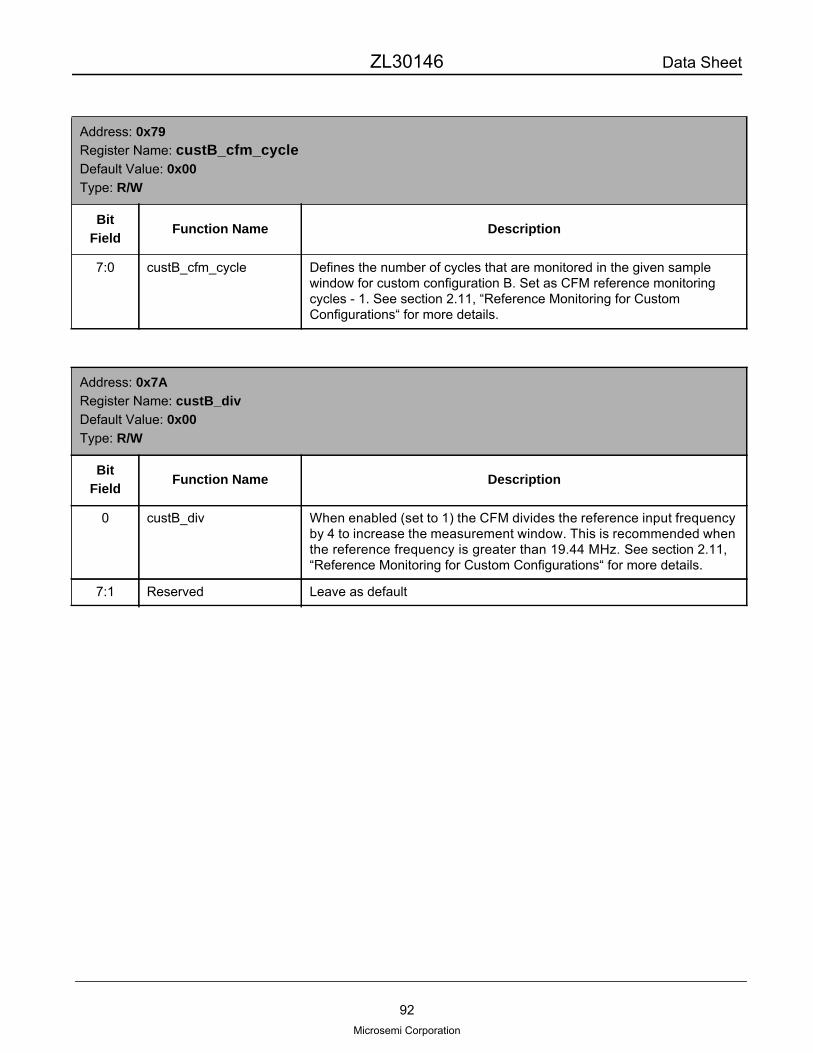
ZL30146 Data Sheet
Address: 0x79Register Name: custB_cfm_cycleDefault Value: 0x00Type: R/W
Bit Field
Function Name Description
7:0 custB_cfm_cycle Defines the number of cycles that are monitored in the given sample window for custom configuration B. Set as CFM reference monitoring cycles - 1. See section 2.11, “Reference Monitoring for Custom Configurations“ for more details.
Address: 0x7ARegister Name: custB_divDefault Value: 0x00Type: R/W
Bit Field
Function Name Description
0 custB_div When enabled (set to 1) the CFM divides the reference input frequency by 4 to increase the measurement window. This is recommended when the reference frequency is greater than 19.44 MHz. See section 2.11, “Reference Monitoring for Custom Configurations“ for more details.
7:1 Reserved Leave as default
92Microsemi Corporation
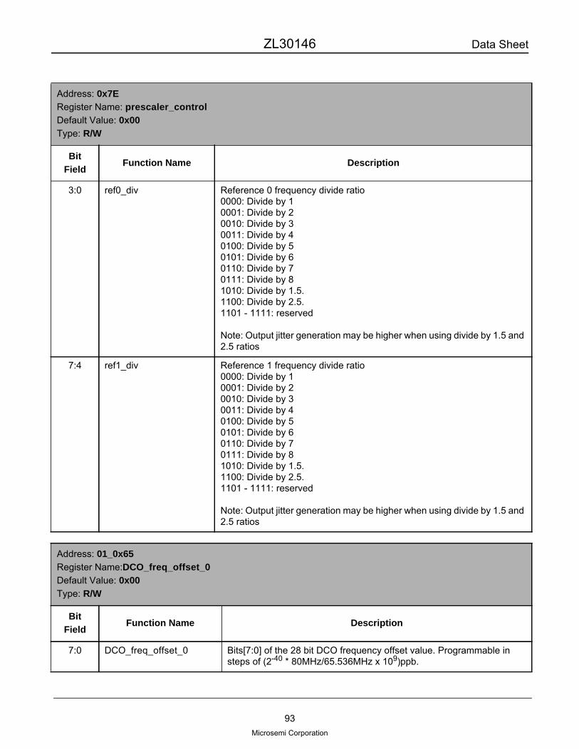
ZL30146 Data Sheet
Address: 0x7ERegister Name: prescaler_controlDefault Value: 0x00Type: R/W
Bit Field
Function Name Description
3:0 ref0_div Reference 0 frequency divide ratio0000: Divide by 10001: Divide by 20010: Divide by 30011: Divide by 40100: Divide by 50101: Divide by 60110: Divide by 70111: Divide by 81010: Divide by 1.5.1100: Divide by 2.5.1101 - 1111: reserved
Note: Output jitter generation may be higher when using divide by 1.5 and 2.5 ratios
7:4 ref1_div Reference 1 frequency divide ratio0000: Divide by 10001: Divide by 20010: Divide by 30011: Divide by 40100: Divide by 50101: Divide by 60110: Divide by 70111: Divide by 81010: Divide by 1.5.1100: Divide by 2.5.1101 - 1111: reserved
Note: Output jitter generation may be higher when using divide by 1.5 and 2.5 ratios
Address: 01_0x65Register Name:DCO_freq_offset_0Default Value: 0x00Type: R/W
Bit Field
Function Name Description
7:0 DCO_freq_offset_0 Bits[7:0] of the 28 bit DCO frequency offset value. Programmable in steps of (2-40 * 80MHz/65.536MHz x 109)ppb.
93Microsemi Corporation
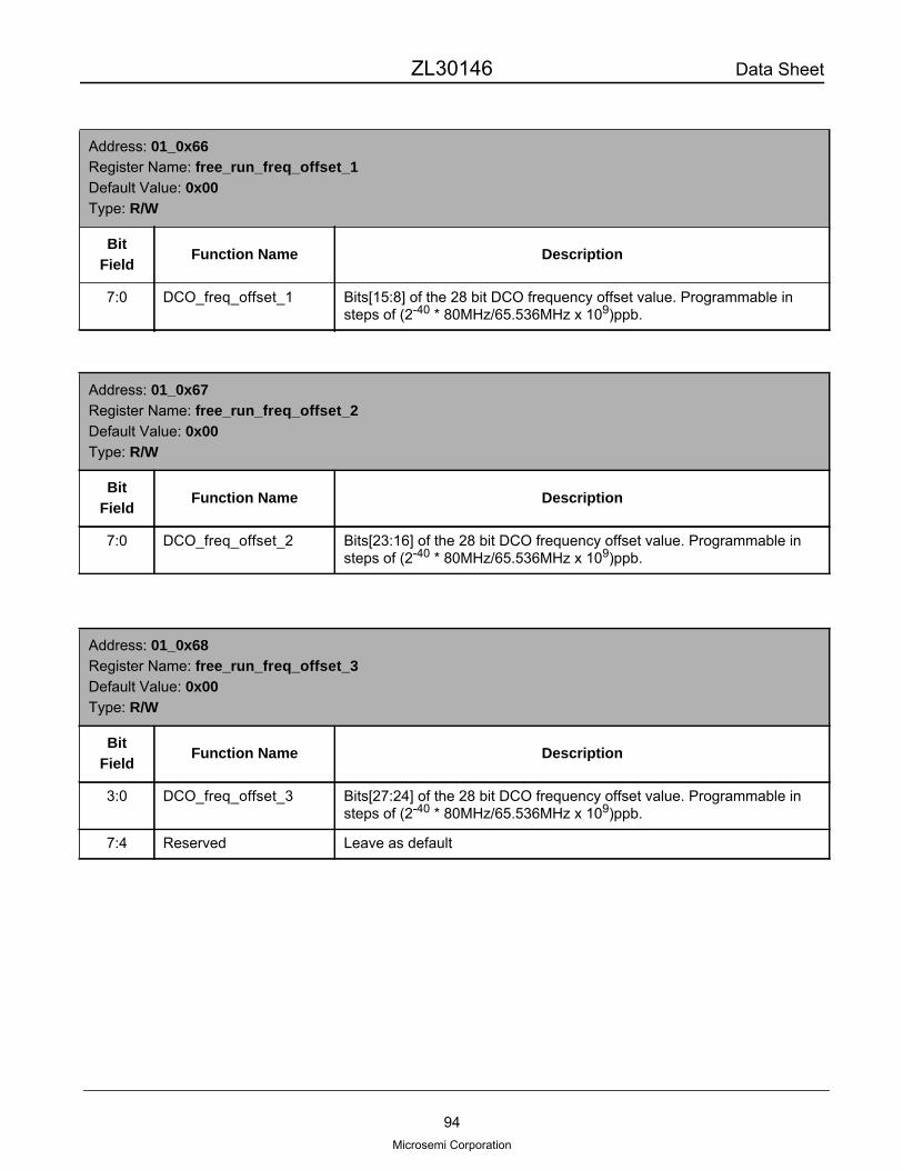
ZL30146 Data Sheet
Address: 01_0x66Register Name: free_run_freq_offset_1Default Value: 0x00Type: R/W
Bit Field
Function Name Description
7:0 DCO_freq_offset_1 Bits[15:8] of the 28 bit DCO frequency offset value. Programmable in steps of (2-40 * 80MHz/65.536MHz x 109)ppb.
Address: 01_0x67Register Name: free_run_freq_offset_2Default Value: 0x00Type: R/W
Bit Field
Function Name Description
7:0 DCO_freq_offset_2 Bits[23:16] of the 28 bit DCO frequency offset value. Programmable in steps of (2-40 * 80MHz/65.536MHz x 109)ppb.
Address: 01_0x68Register Name: free_run_freq_offset_3Default Value: 0x00Type: R/W
Bit Field
Function Name Description
3:0 DCO_freq_offset_3 Bits[27:24] of the 28 bit DCO frequency offset value. Programmable in steps of (2-40 * 80MHz/65.536MHz x 109)ppb.
7:4 Reserved Leave as default
94Microsemi Corporation
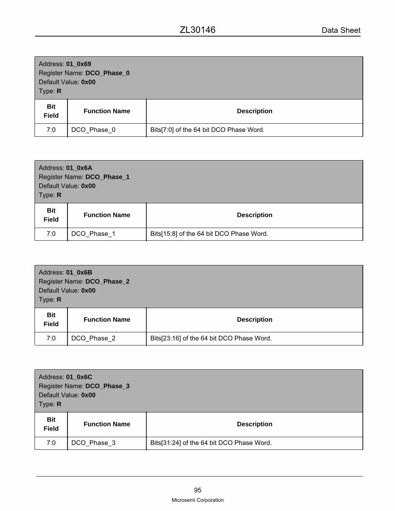
ZL30146 Data Sheet
Address: 01_0x69Register Name: DCO_Phase_0Default Value: 0x00Type: R
Bit Field
Function Name Description
7:0 DCO_Phase_0 Bits[7:0] of the 64 bit DCO Phase Word.
Address: 01_0x6ARegister Name: DCO_Phase_1Default Value: 0x00Type: R
Bit Field
Function Name Description
7:0 DCO_Phase_1 Bits[15:8] of the 64 bit DCO Phase Word.
Address: 01_0x6BRegister Name: DCO_Phase_2Default Value: 0x00Type: R
Bit Field
Function Name Description
7:0 DCO_Phase_2 Bits[23:16] of the 64 bit DCO Phase Word.
Address: 01_0x6CRegister Name: DCO_Phase_3Default Value: 0x00Type: R
Bit Field
Function Name Description
7:0 DCO_Phase_3 Bits[31:24] of the 64 bit DCO Phase Word.
95Microsemi Corporation

ZL30146 Data Sheet
Address: 01_0x6DRegister Name: DCO_Phase_4Default Value: 0x00Type: R
Bit Field
Function Name Description
7:0 DCO_Phase_4 Bits[39:32] of the 64 bit DCO Phase Word.
Address: 01_0x6ERegister Name: DCO_Phase_5Default Value: 0x00Type: R
Bit Field
Function Name Description
7:0 DCO_Phase_5 Bits[47:40] of the 64 bit DCO Phase Word.
Address: 01_0x6FRegister Name: DCO_Phase_6Default Value: 0x00Type: R
Bit Field
Function Name Description
7:0 DCO_Phase_6 Bits[55:48] of the 64 bit DCO Phase Word.
Address: 01_0x70Register Name: DCO_Phase_7Default Value: 0x00Type: R
Bit Field
Function Name Description
7:0 DCO_Phase_7 Bits[63:56] of the 64 bit DCO Phase Word.
96Microsemi Corporation

ZL30146 Data Sheet
Address: 01_0x71Register Name: Local_Time_0Default Value: 0x00Type: R
Bit Field
Function Name Description
7:0 Local_Time_0 Bits[7:0] of the 32 bit Local System Time.
Address: 01_0x72Register Name: Local_Time_1Default Value: 0x00Type: R
Bit Field
Function Name Description
7:0 Local_Time_1 Bits[15:8] of the 32 bit Local System Time.
Address: 01_0x73Register Name: Local_Time_2Default Value: 0x00Type: R
Bit Field
Function Name Description
7:0 Local_Time_2 Bits[23:16] of the 32 bit Local System Time.
Address: 01_0x74Register Name: Local_Time_3Default Value: 0x00Type: R
Bit Field
Function Name Description
7:0 Local_Time_3 Bits[31:24] of the 32 bit Local System Time.
97Microsemi Corporation
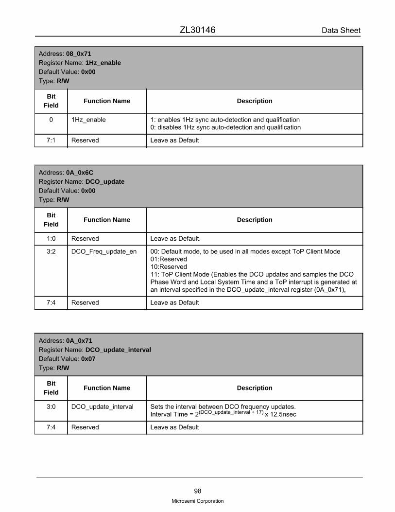
ZL30146 Data Sheet
Address: 08_0x71Register Name: 1Hz_enableDefault Value: 0x00Type: R/W
Bit Field
Function Name Description
0 1Hz_enable 1: enables 1Hz sync auto-detection and qualification0: disables 1Hz sync auto-detection and qualification
7:1 Reserved Leave as Default
Address: 0A_0x6CRegister Name: DCO_updateDefault Value: 0x00Type: R/W
Bit Field
Function Name Description
1:0 Reserved Leave as Default.
3:2 DCO_Freq_update_en 00: Default mode, to be used in all modes except ToP Client Mode01:Reserved10:Reserved11: ToP Client Mode (Enables the DCO updates and samples the DCO Phase Word and Local System Time and a ToP interrupt is generated at an interval specified in the DCO_update_interval register (0A_0x71),
7:4 Reserved Leave as Default
Address: 0A_0x71Register Name: DCO_update_intervalDefault Value: 0x07Type: R/W
Bit Field
Function Name Description
3:0 DCO_update_interval Sets the interval between DCO frequency updates.Interval Time = 2(DCO_update_interval + 17) x 12.5nsec
7:4 Reserved Leave as Default
98Microsemi Corporation
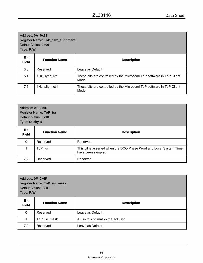
ZL30146 Data Sheet
Address: 0A_0x72Register Name: ToP_1Hz_alignmentlDefault Value: 0x00Type: R/W
Bit Field
Function Name Description
3:0 Reserved Leave as Default
5:4 1Hz_sync_ctrl These bits are controlled by the Microsemi ToP software in ToP Client Mode
7:6 1Hz_align_ctrl These bits are controlled by the Microsemi ToP software in ToP Client Mode
Address: 0F_0x6ERegister Name: ToP_isrDefault Value: 0x10Type: Sticky R
Bit Field
Function Name Description
0 Reserved Reserved
1 ToP_isr This bit is asserted when the DCO Phase Word and Local System Time have been sampled
7:2 Reserved Reserved
Address: 0F_0x6FRegister Name: ToP_isr_maskDefault Value: 0x1FType: R/W
Bit Field
Function Name Description
0 Reserved Leave as Default
1 ToP_isr_mask A 0 in this bit masks the ToP_isr
7:2 Reserved Leave as Default
99Microsemi Corporation
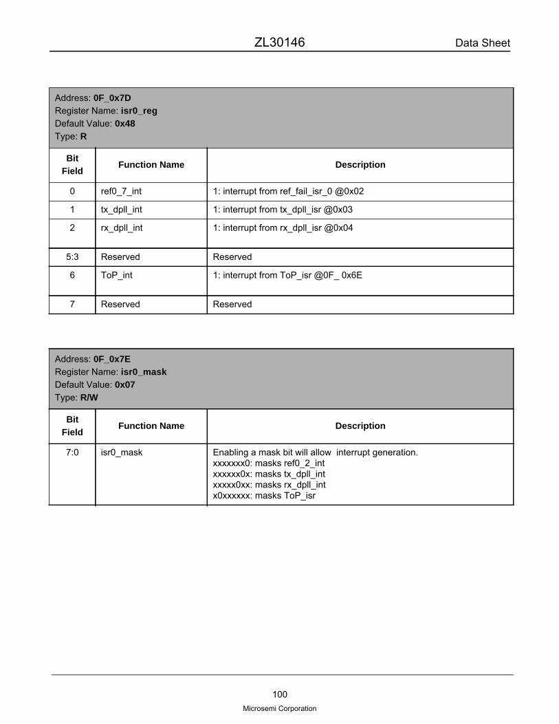
ZL30146 Data Sheet
Address: 0F_0x7DRegister Name: isr0_regDefault Value: 0x48Type: R
Bit Field
Function Name Description
0 ref0_7_int 1: interrupt from ref_fail_isr_0 @0x02
1 tx_dpll_int 1: interrupt from tx_dpll_isr @0x03
2 rx_dpll_int 1: interrupt from rx_dpll_isr @0x04
5:3 Reserved Reserved
6 ToP_int 1: interrupt from ToP_isr @0F_ 0x6E
7 Reserved Reserved
Address: 0F_0x7ERegister Name: isr0_maskDefault Value: 0x07Type: R/W
Bit Field
Function Name Description
7:0 isr0_mask Enabling a mask bit will allow interrupt generation.xxxxxxx0: masks ref0_2_intxxxxxx0x: masks tx_dpll_intxxxxx0xx: masks rx_dpll_intx0xxxxxx: masks ToP_isr
100Microsemi Corporation
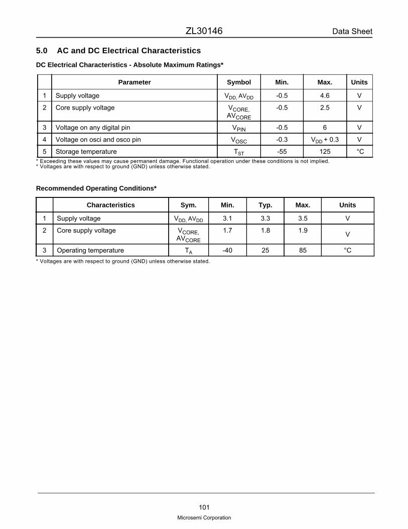
ZL30146 Data Sheet
5.0 AC and DC Electrical CharacteristicsDC Electrical Characteristics - Absolute Maximum Ratings*
* Exceeding these values may cause permanent damage. Functional operation under these conditions is not implied.* Voltages are with respect to ground (GND) unless otherwise stated.
Recommended Operating Conditions*
* Voltages are with respect to ground (GND) unless otherwise stated.
Parameter Symbol Min. Max. Units
1 Supply voltage VDD, AVDD -0.5 4.6 V
2 Core supply voltage VCORE, AVCORE
-0.5 2.5 V
3 Voltage on any digital pin VPIN -0.5 6 V
4 Voltage on osci and osco pin VOSC -0.3 VDD + 0.3 V
5 Storage temperature TST -55 125 °C
Characteristics Sym. Min. Typ. Max. Units
1 Supply voltage VDD, AVDD 3.1 3.3 3.5 V
2 Core supply voltage VCORE, AVCORE
1.7 1.8 1.9 V
3 Operating temperature TA -40 25 85 °C
101Microsemi Corporation
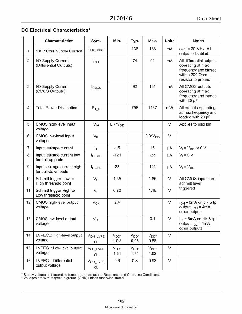
ZL30146 Data Sheet
DC Electrical Characteristics*
* Supply voltage and operating temperature are as per Recommended Operating Conditions.* Voltages are with respect to ground (GND) unless otherwise stated.
Characteristics Sym. Min. Typ. Max. Units Notes
1 1.8 V Core Supply Current I1.8_CORE 138 188 mA osci = 20 MHz, All outputs disabled.
2 I/O Supply Current (Differential Outputs)
IDIFF 74 92 mA All differential outputs operating at max frequency and biased with a 200 Ohm resistor to ground
3 I/O Supply Current (CMOS Outputs)
ICMOS 92 131 mA All CMOS outputs operating at max frequency and loaded with 20 pF
4 Total Power Dissipation PT_D 796 1137 mW All outputs operating at max frequency and loaded with 20 pF
5 CMOS high-level input voltage
VIH 0.7*VDD V Applies to osci pin
6 CMOS low-level input voltage
VIL 0.3*VDD V
7 Input leakage current IIL -15 15 μA VI = VDD or 0 V
8 Input leakage current low for pull-up pads
IIL_PU -121 -23 μA VI = 0 V
9 Input leakage current high for pull-down pads
IIL_PD 23 121 μA VI = VDD
10 Schmitt trigger Low to High threshold point
Vt+ 1.35 1.85 V All CMOS inputs are schmitt level triggered11 Schmitt trigger High to
Low threshold pointVt- 0.80 1.15 V
12 CMOS high-level output voltage
VOH 2.4 V IOH = 8mA on clk & fp output. IOH = 4mA other outputs
13 CMOS low-level output voltage
VOL 0.4 V IOL= 8mA on clk & fp output. IOL = 4mA other outputs
14 LVPECL: High-level output voltage
VOH_LVPE
CL
VDD- 1.0.8
VDD- 0.96
VDD- 0.88
V
15 LVPECL: Low-level output voltage
VOL_LVPE
CL
VDD- 1.81
VDD- 1.71
VDD- 1.62
V
16 LVPECL: Differential output voltage
VOD_LVPE
CL
0.6 0.8 0.93 V
102Microsemi Corporation
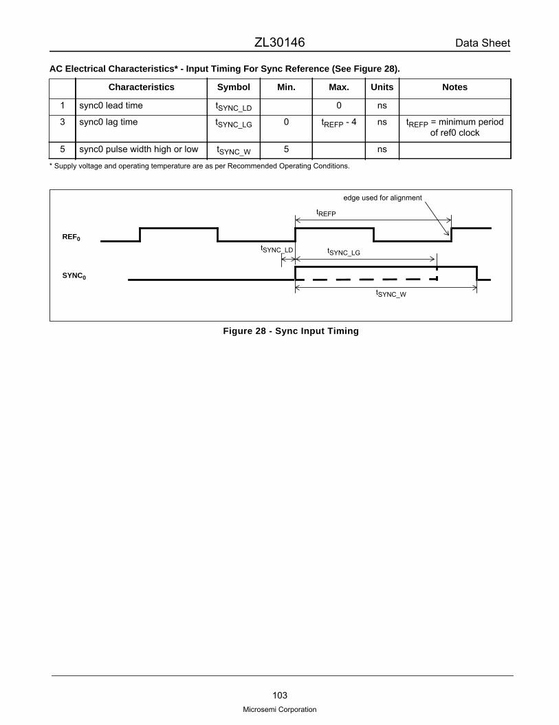
ZL30146 Data Sheet
AC Electrical Characteristics* - Input Timing For Sync Reference (See Figure 28).
* Supply voltage and operating temperature are as per Recommended Operating Conditions.
Figure 28 - Sync Input Timing
Characteristics Symbol Min. Max. Units Notes
1 sync0 lead time tSYNC_LD 0 ns
3 sync0 lag time tSYNC_LG 0 tREFP - 4 ns tREFP = minimum period of ref0 clock
5 sync0 pulse width high or low tSYNC_W 5 ns
REF0
SYNC0
tSYNC_LD tSYNC_LG
tSYNC_W
tREFP
edge used for alignment
103Microsemi Corporation
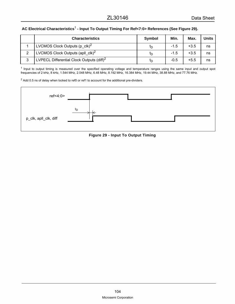
ZL30146 Data Sheet
AC Electrical Characteristics1 - Input To Output Timing For Ref<7:0> References (See Figure 29).
1 Input to output timing is measured over the specified operating voltage and temperature ranges using the same input and output spotfrequencies of 2 kHz, 8 kHz, 1.544 MHz, 2.048 MHz, 6.48 MHz, 8.192 MHz, 16.384 MHz, 19.44 MHz, 38.88 MHz, and 77.76 MHz.
2 Add 0.5 ns of delay when locked to ref0 or ref1 to account for the additional pre-dividers.
Figure 29 - Input To Output Timing
Characteristics Symbol Min. Max. Units
1 LVCMOS Clock Outputs (p_clk)2 tD -1.5 +3.5 ns
2 LVCMOS Clock Outputs (apll_clk)2 tD -1.5 +3.5 ns
3 LVPECL Differential Clock Outputs (diff)2 tD -0.5 +5.5 ns
ref<4:0>
tD
p_clk, apll_clk, diff
104Microsemi Corporation
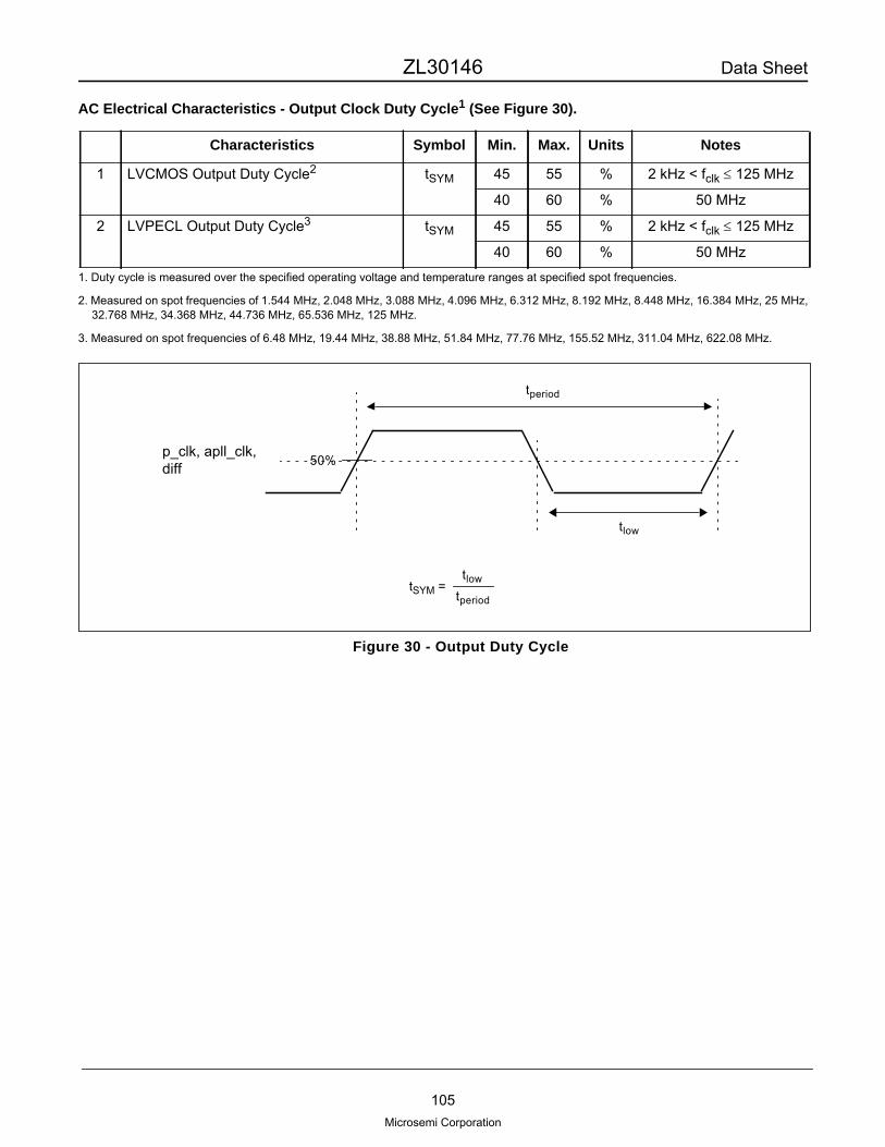
ZL30146 Data Sheet
AC Electrical Characteristics - Output Clock Duty Cycle1 (See Figure 30).
1. Duty cycle is measured over the specified operating voltage and temperature ranges at specified spot frequencies.
2. Measured on spot frequencies of 1.544 MHz, 2.048 MHz, 3.088 MHz, 4.096 MHz, 6.312 MHz, 8.192 MHz, 8.448 MHz, 16.384 MHz, 25 MHz, 32.768 MHz, 34.368 MHz, 44.736 MHz, 65.536 MHz, 125 MHz.
3. Measured on spot frequencies of 6.48 MHz, 19.44 MHz, 38.88 MHz, 51.84 MHz, 77.76 MHz, 155.52 MHz, 311.04 MHz, 622.08 MHz.
Figure 30 - Output Duty Cycle
Characteristics Symbol Min. Max. Units Notes
1 LVCMOS Output Duty Cycle2 tSYM 45 55 % 2 kHz < fclk 125 MHz
40 60 % 50 MHz
2 LVPECL Output Duty Cycle3 tSYM 45 55 % 2 kHz < fclk 125 MHz
40 60 % 50 MHz
p_clk, apll_clk, diff
tperiod
tlow
tlow tperiod
tSYM =
50%
105Microsemi Corporation
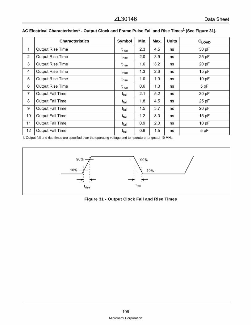
ZL30146 Data Sheet
AC Electrical Characteristics* - Output Clock and Frame Pulse Fall and Rise Times1 (See Figure 31).
1. Output fall and rise times are specified over the operating voltage and temperature ranges at 10 MHz.
Figure 31 - Output Clock Fall and Rise Times
Characteristics Symbol Min. Max. Units CLOAD
1 Output Rise Time trise 2.3 4.5 ns 30 pF
2 Output Rise Time trise 2.0 3.9 ns 25 pF
3 Output Rise Time trise 1.6 3.2 ns 20 pF
4 Output Rise Time trise 1.3 2.6 ns 15 pF
5 Output Rise Time trise 1.0 1.9 ns 10 pF
6 Output Rise Time trise 0.6 1.3 ns 5 pF
7 Output Fall Time tfall 2.1 5.2 ns 30 pF
8 Output Fall Time tfall 1.8 4.5 ns 25 pF
9 Output Fall Time tfall 1.5 3.7 ns 20 pF
10 Output Fall Time tfall 1.2 3.0 ns 15 pF
11 Output Fall Time tfall 0.9 2.3 ns 10 pF
12 Output Fall Time tfall 0.6 1.5 ns 5 pF
trise
10%
90%
10%
90%
tfall
106Microsemi Corporation
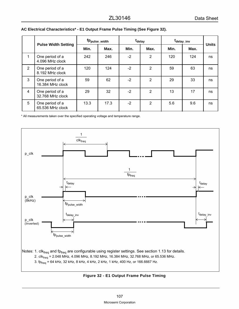
ZL30146 Data Sheet
AC Electrical Characteristics* - E1 Output Frame Pulse Timing (See Figure 32).
* All measurements taken over the specified operating voltage and temperature range.
Figure 32 - E1 Output Frame Pulse Timing
Pulse Width Settingfppulse_width tdelay tdelay_inv
UnitsMin. Max. Min. Max. Min. Max.
1 One period of a 4.096 MHz clock
242 246 -2 2 120 124 ns
2 One period of a 8.192 MHz clock
120 124 -2 2 59 63 ns
3 One period of a 16.384 MHz clock
59 62 -2 2 29 33 ns
4 One period of a 32.768 MHz clock
29 32 -2 2 13 17 ns
5 One period of a 65.536 MHz clock
13.3 17.3 -2 2 5.6 9.6 ns
tdelay
(Inverted)
tdelay_inv
p_clk
p_clk
p_clk
fppulse_width
fppulse_width
3. fpfreq = 64 kHz, 32 kHz, 8 kHz, 4 kHz, 2 kHz, 1 kHz, 400 Hz, or 166.6667 Hz.
fpfreq
2. clkfreq = 2.048 MHz, 4.096 MHz, 8.192 MHz, 16.384 MHz, 32.768 MHz, or 65.536 MHz. Notes: 1. clkfreq and fpfreq are configurable using register settings. See section 1.13 for details.
tdelay
tdelay_inv
clkfreq 1
1
(8kHz)
107Microsemi Corporation
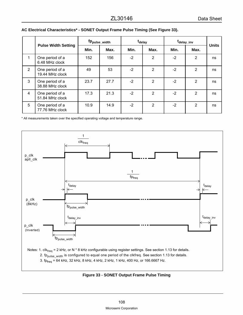
ZL30146 Data Sheet
AC Electrical Characteristics* - SONET Output Frame Pulse Timing (See Figure 33).
* All measurements taken over the specified operating voltage and temperature range.
Figure 33 - SONET Output Frame Pulse Timing
Pulse Width Settingfppulse_width tdelay tdelay_inv
UnitsMin. Max. Min. Max. Min. Max.
1 One period of a 6.48 MHz clock
152 156 -2 2 -2 2 ns
2 One period of a 19.44 MHz clock
49 53 -2 2 -2 2 ns
3 One period of a 38.88 MHz clock
23.7 27.7 -2 2 -2 2 ns
4 One period of a 51.84 MHz clock
17.3 21.3 -2 2 -2 2 ns
5 One period of a 77.76 MHz clock
10.9 14.9 -2 2 -2 2 ns
3. fpfreq = 64 kHz, 32 kHz, 8 kHz, 4 kHz, 2 kHz, 1 kHz, 400 Hz, or 166.6667 Hz. 2. fppulse_width is configured to equal one period of the clkfreq. See section 1.13 for details.
Notes: 1. clkfreq = 2 kHz, or N * 8 kHz configurable using register settings. See section 1.13 for details.
tdelay
(Inverted)
tdelay_inv
p_clk
fppulse_width
fppulse_width
fpfreq
tdelay
tdelay_inv
clkfreq 1
1
(8kHz)
apll_clk
p_clk
p_clk
108Microsemi Corporation
ZL30146 Data Sheet
AC Electrical Characteristics - Serial Peripheral Interface Timing
Table 10 - Serial Peripheral Interface Timing
Figure 34 - Serial Peripheral Interface Timing - LSB First Mode
Figure 35 - Serial Peripheral Interface Timing - MSB First Mode
Specification Name Min. Max. Units
sck period tcyc 124 nssck pulse width low tclkl 62 nssck pulse width high tclkh 62 nssi setup (write) from sck rising trxs 10 nssi hold (write) from sck rising trxh 10 nsso delay (read) from sck falling txd 25 nscs_b setup from sck falling (LSB first) tcssi 20 nscs_b setup from sck rising (MSB first) tcssm 20 nscs_b hold from sck falling (MSB first) tcshm 10 nscs_b hold from sck rising (LSB first) tcshi 10 nscs_b to output high impedance tohz 60 ns
si
sck
cs_b
trxstrxh
tclkl
tclkh
tcyc tcshi tcssi
so
tohztxd
si
sck
cs_b
trxstrxh
tclkl
tclkh
tcyc tcshi tcssm
so
tohz
txd
109Microsemi Corporation
ZL30146 Data Sheet
AC Electrical Characteristics - I2C Timing
Figure 36 - I2C Serial Microport Timing
Specification Name Min. Typ. Max. Units Note
SCL clock frequency fSCL 0 400 kHzHold time START condition tHD:STA 0.6 usLow period SCL tLOW 1.3 usHi period SCL tHIGH 0.6 usSetup time START condition tSU:STA 0.6 usData hold time tHD:DAT 0 0.9 usData setup time tSU:DAT 100 nsRise time tr ns Determined by pull-up
resistorFall time tf 20 +
0.1Cb
250 ns
Setup time STOP condition tSU:STO 0.6 usBus free time between STOP/START
tBUF 1.3 us
Pulse width of spikes which must be suppressed by the input filter
tSP 0 50 ns
Max capacitance for each I/O pin
10 pF
Table 11 - I2C Serial Microport Timing
SDA
SCL
tf
S
tLOW tr
tHD:STAtHD:DAT
tSU:DAT
tHIGH
tf
tSU:STA Sr
tHD:STA tSP tBUF
tSU:STOP S
110Microsemi Corporation
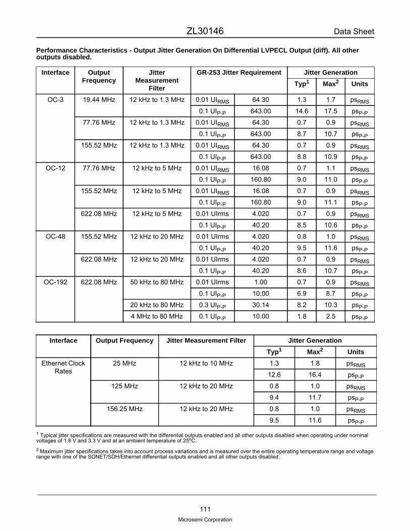
ZL30146 Data Sheet
Performance Characteristics - Output Jitter Generation On Differential LVPECL Output (diff). All other outputs disabled.
1 Typical jitter specifications are measured with the differential outputs enabled and all other outputs disabled when operating under nominal voltages of 1.8 V and 3.3 V and at an ambient temperature of 25oC. 2 Maximum jitter specifications takes into account process variations and is measured over the entire operating temperature range and voltage range with one of the SONET/SDH/Ethernet differential outputs enabled and all other outputs disabled.
Interface Output Frequency
Jitter Measurement
Filter
GR-253 Jitter Requirement Jitter Generation Typ1 Max2 Units
OC-3 19.44 MHz 12 kHz to 1.3 MHz 0.01 UIRMS 64.30 1.3 1.7 psRMS
0.1 UIP-P 643.00 14.6 17.5 psP-P
77.76 MHz 12 kHz to 1.3 MHz 0.01 UIRMS 64.30 0.7 0.9 psRMS
0.1 UIP-P 643.00 8.7 10.7 psP-P
155.52 MHz 12 kHz to 1.3 MHz 0.01 UIRMS 64.30 0.7 0.9 psRMS
0.1 UIP-P 643.00 8.8 10.9 psP-P
OC-12 77.76 MHz 12 kHz to 5 MHz 0.01 UIRMS 16.08 0.7 1.1 psRMS
0.1 UIP-P 160.80 9.0 11.0 psP-P
155.52 MHz 12 kHz to 5 MHz 0.01 UIRMS 16.08 0.7 0.9 psRMS
0.1 UIP-P 160.80 9.0 11.1 psP-P
622.08 MHz 12 kHz to 5 MHz 0.01 UIrms 4.020 0.7 0.9 psRMS
0.1 UIP-P 40.20 8.5 10.6 psP-P
OC-48 155.52 MHz 12 kHz to 20 MHz 0.01 UIrms 4.020 0.8 1.0 psRMS
0.1 UIP-P 40.20 9.5 11.6 psP-P
622.08 MHz 12 kHz to 20 MHz 0.01 UIrms 4.020 0.7 0.9 psRMS
0.1 UIP-P 40.20 8.6 10.7 psP-P
OC-192 622.08 MHz 50 kHz to 80 MHz 0.01 UIrms 1.00 0.7 0.9 psRMS
0.1 UIP-P 10.00 6.9 8.7 psP-P
20 kHz to 80 MHz 0.3 UIP-P 30.14 8.2 10.3 psP-P
4 MHz to 80 MHz 0.1 UIP-P 10.00 1.8 2.5 psP-P
Interface Output Frequency Jitter Measurement Filter Jitter Generation Typ1 Max2 Units
Ethernet Clock Rates
25 MHz 12 kHz to 10 MHz 1.3 1.8 psRMS
12.6 16.4 psP-P
125 MHz 12 kHz to 20 MHz 0.8 1.0 psRMS
9.4 11.7 psP-P
156.25 MHz 12 kHz to 20 MHz 0.8 1.0 psRMS
9.5 11.6 psP-P
111Microsemi Corporation
ZL30146 Data Sheet
Performance Characteristics - Output Jitter Generation On Differential LVPECL Outputs (diff). All other outputs enabled.
1 Typical jitter specifications are measured under the power-up default configuration when operating under nominal voltages of 1.8 V and 3.3 V and at an ambient temperature of 25oC. 2 Maximum jitter specifications takes into account process variations and is measured over the entire operating temperature range and voltage range with all other outputs enabled while generating any of the frequencies available from the SONET/SDH/Ethernet synthesizer and any of the programmable frequencies on the programmable outputs up to 65.536 MHz.
Interface Output Frequency
Jitter Measurement
Filter
GR-253 Jitter Requirement Jitter Generation Typ1 Max2 Units
OC-3 19.44 MHz 12 kHz to 1.3 MHz 0.01 UIRMS 64.30 1.6 2.3 psRMS
0.1 UIP-P 643.00 15.4 19.7 psP-P
77.76 MHz 12 kHz to 1.3 MHz 0.01 UIRMS 64.30 0.8 1.3 psRMS
0.1 UIP-P 643.00 9.2 12.4 psP-P
155.52 MHz 12 kHz to 1.3 MHz 0.01 UIRMS 64.30 0.8 1.3 psRMS
0.1 UIP-P 643.00 9.3 12.7 psP-P
OC-12 77.76 MHz 12 kHz to 5 MHz 0.01 UIRMS 16.08 0.9 1.5 psRMS
0.1 UIP-P 160.80 9.6 13.3 psP-P
155.52 MHz 12 kHz to 5 MHz 0.01 UIRMS 16.08 0.9 1.4 psRMS
0.1 UIP-P 160.80 9.6 13.3 psP-P
622.08 MHz 12 kHz to 5 MHz 0.01 UIrms 4.020 0.8 1.4 psRMS
0.1 UIP-P 40.20 9.1 12.9 psP-P
OC-48 155.52 MHz 12 kHz to 20 MHz 0.01 UIrms 4.020 1.0 1.5 psRMS
0.1 UIP-P 40.20 10.1 13.7 psP-P
622.08 MHz 12 kHz to 20 MHz 0.01 UIrms 4.020 0.8 1.4 psRMS
0.1 UIP-P 40.20 9.2 13.0 psP-P
OC-192 622.08 MHz 50 kHz to 80 MHz 0.01 UIrms 1.00 0.7 1.0 psRMS
0.1 UIP-P 10.00 7.3 9.2 psP-P
20 kHz to 80 MHz 0.3 UIP-P 30.14 8.6 10.7 psP-P
4 MHz to 80 MHz 0.1 UIP-P 10.00 2.1 3.2 psP-P
Interface Output Frequency Jitter Measurement Filter Jitter Generation Typ1 Max2 Units
Ethernet Clock Rates
25 MHz 12 kHz to 10 MHz 1.4 1.9 psRMS
13.0 16.7 psP-P
125 MHz 12 kHz to 20 MHz 0.8 1.0 psRMS
9.5 11.7 psP-P
156.25 MHz 12 kHz to 20 MHz 0.9 1.1 psRMS
9.7 11.8 psP-P
112Microsemi Corporation
ZL30146 Data Sheet
Performance Characteristics - Output Jitter Generation On Differential LVPECL Outputs (diff). All other outputs enabled.
1 Typical jitter specifications are measured under the power-up default configuration when operating under nominal voltages of 1.8 V and 3.3 V and at an ambient temperature of 25oC. 2 Maximum jitter specifications takes into account process variations and is measured over the entire operating temperature range and voltage range with all other outputs enabled while generating any of the frequencies available from the SONET/SDH/Ethernet synthesizer and any of the programmable frequencies on the programmable outputs up to 65.536 MHz.
Interface Output Frequency
Jitter Measurement
Filter
G.813 Jitter Requirement Jitter Generation
Typ1 Max2 Units
Option 1
STM-1 19.44 MHz 65 kHz to 1.3 MHz 0.1 UIP-P 643 13.9 17.8 psP-P
500 Hz to 1.3 MHz 0.5 UIP-P 3215 16.3 20.6 psP-P
77.76 MHz 65 kHz to 1.3 MHz 0.1 UIP-P 643 6.8 9.7 psP-P
500 Hz to 1.3 MHz 0.5 UIP-P 3215 10.3 13.6 psP-P
155.52 MHz 65 kHz to 1.3 MHz 0.1 UIP-P 643 6.8 9.8 psP-P
500 Hz to 1.3 MHz 0.5 UIP-P 3215 10.5 13.9 psP-P
STM-4 77.76 MHz 250 kHz to 5 MHz 0.1 UIP-P 161 4.8 8.4 psP-P
1 kHz to 5 MHz 0.5 UIP-P 804 10.5 14.2 psP-P
155.52 MHz 250 kHz to 5 MHz 0.1 UIP-P 161 4.4 5.6 psP-P
1 kHz to 5 MHz 0.5 UIP-P 804 10.5 14.3 psP-P
622.08 MHz 250 kHz to 5 MHz 0.1 UIP-P 161 3.9 5.0 psP-P
1 kHz to 5 MHz 0.5 UIP-P 804 10.0 13.9 psP-P
STM-16 155.52 MHz 1 MHz to 20 MHz 0.1 UIP-P 40.2 4.0 5.4 psP-P
5 kHz to 20 MHz 0.5 UIP-P 201 10.6 14.3 psP-P
622.08 MHz 1 MHz to 20 MHz 0.1 UIP-P 40.2 2.4 4.4 psP-P
5 kHz to 20 MHz 0.5 UIP-P 201 9.7 13.6 psP-P
STM-64 622.08 MHz 4 MHz to 80 MHz 0.1 UIP-P 10 2.1 3.2 psP-P
20 kHz to 80 MHz 0.5 UIP-P 50.2 8.7 10.7 psP-P
Option 2
STM-1 77.76 MHz 12 kHz to 1.3 MHz 0.1 UIP-P 643 9.1 12.4 psP-P
155.52 MHz 12 kHz to 1.3 MHz 0.1 UIP-P 643 9.3 12.7 psP-P
STM-4 77.76 MHz 12 kHz to 5 MHz 0.1 UIP-P 161 9.6 13.3 psP-P
155.52 MHz 12 kHz to 5 MHz 0.1 UIP-P 161 9.6 13.3 psP-P
622.08 MHz 12 kHz to 5 MHz 0.1 UIP-P 161 9.1 12.9 psP-P
STM-16 155.52 MHz 12 kHz to 20 MHz 0.1 UIP-P 40.2 10.1 13.7 psP-P
622.08 MHz 12 kHz to 20 MHz 0.1 UIP-P 40.2 9.2 13.0 psP-P
STM-64 622.08 MHz 4 MHz to 80 MHz 0.1 UIP-P 10 2.1 3.2 psP-P
20 kHz to 80 MHz 0.3 UIP-P 30.1 8.6 10.7 psP-P
113Microsemi Corporation
ZL30146 Data Sheet
Performance Characteristics - Measured Output Jitter On APLL CMOS Output (apll_clk). All other outputs enabled.
1 Typical jitter specifications are measured when operating at nominal voltages of 1.8 V and 3.3 V and at an ambient temperature of 25oC. 2 Maximum jitter specifications takes into account process variations and is measured over the entire operating temperature range and voltage range with all outputs enabled.
Performance Characteristics - Measured Output Jitter On Programmable CMOS Output (p_clk).
1 Typical jitter specifications are measured when operating at nominal voltages of 1.8 V and 3.3 V and at an ambient temperature of 25oC. 2 Maximum jitter specifications takes into account process variations and is measured over the entire operating temperature range and voltage range with all outputs enabled.
6.0 Thermal Characteristics
Output Frequency Jitter Measurement Filter Jitter Generation
Typ1 Max2 Units
SONET/SDH6.48 MHz, 19.44 MHz, 38.88 MHz, 51.84 MHz,
77.76 MHz
12 kHz to 5 MHz 2.3 3.1 psRMS
22.8 28.7 psP-P
unfiltered 3.2 4.3 psRMS
33.1 42.0 psP-P
Ethernet25 MHz
637 kHz to Nyquist 1.7 2.9 psRMS
11.8 19.6 psP-P
12 kHz to 10 MHz 1.8 2.9 psRMS
15.2 22.8 psP-P
Ethernet125 MHz
637 kHz to Nyquist 0.6 1.0 psRMS
5.0 8.9 psP-P
12 kHz to 20 MHz 0.9 1.4 psRMS
10.4 14.2 psP-P
Output Frequency Jitter Measurement Filter Jitter Generation
Typ1 Max2 Units
8 kHz to 100 MHz unfiltered 18.0 24.0 psRMS
Parameter Symbol Test Condition Value Unit
Junction to Ambient Thermal Resistance ja Still Air 31.6 oC/W
Junction to Case Thermal Resistance jc Still Air 10.3 oC/W
Table 12 - Thermal Data
114Microsemi Corporation
c Zarlink Semiconductor 2005 All rights reserved.
ISSUE
APPRD.
DATE
ACN
Package Code
Previous package codes
Copyright 2013, Microsemi Corporation. All Rights Reserved.
MiOnWiSaFa
Information relating to products and services furnished herein by Microsemi Corporation or its subsidiaries (collectively “Microsemi”) isbelieved to be reliable. However, Microsemi assumes no liability for errors that may appear in this publication, or for liability otherwisearising from the application or use of any such information, product or service or for any infringement of patents or other intellectualproperty rights owned by third parties which may result from such application or use. Neither the supply of such information orpurchase of product or service conveys any license, either express or implied, under patents or other intellectual property rights ownedby Microsemi or licensed from third parties by Microsemi, whatsoever. Purchasers of products are also hereby notified that the use ofproduct in certain ways or in combination with Microsemi, or non-Microsemi furnished goods or services may infringe patents or otherintellectual property rights owned by Microsemi.
This publication is issued to provide information only and (unless agreed by Microsemi in writing) may not be used, applied orreproduced for any purpose nor form part of any order or contract nor to be regarded as a representation relating to the products orservices concerned. The products, their specifications, services and other information appearing in this publication are subject tochange by Microsemi without notice. No warranty or guarantee express or implied is made regarding the capability, performance orsuitability of any product or service. Information concerning possible methods of use is provided as a guide only and does notconstitute any guarantee that such methods of use will be satisfactory in a specific piece of equipment. It is the user’s responsibility tofully determine the performance and suitability of any equipment using such information and to ensure that any publication or data usedis up to date and has not been superseded. Manufacturing does not necessarily include testing of all functions or parameters. Theseproducts are not suitable for use in any medical and other products whose failure to perform may result in significant injury or death tothe user. All products and materials are sold and services provided subject to Microsemi’s conditions of sale which are available onrequest.
For more information about all Microsemi productsvisit our website at
www.microsemi.com
TECHNICAL DOCUMENTATION – NOT FOR RESALE
© 2013 Microsemi Corporation. All rights reserved. Microsemi and the Microsemi logo are trademarks ofMicrosemi Corporation. All other trademarks and service marks are the property of their respective owners.
Microsemi Corporation (NASDAQ: MSCC) offers a comprehensive portfolio of semiconductorsolutions for: aerospace, defense and security; enterprise and communications; and industrialand alternative energy markets. Products include high-performance, high-reliability analog andRF devices, mixed signal and RF integrated circuits, customizable SoCs, FPGAs, andcomplete subsystems. Microsemi is headquartered in Aliso Viejo, Calif. Learn more atwww.microsemi.com.
crosemi Corporate Headquarterse Enterprise, Aliso Viejo CA 92656 USAthin the USA: +1 (949) 380-6100
les: +1 (949) 380-6136x: +1 (949) 215-4996ZL30146