Embed Size (px)
Citation preview
Chapter 1
OrCAD/ModelSim Tutorial for CPLDs
This tutorial shows you how to use OrCAD Capture’s Schematic module and Express module for compiling XC9500/XL/XV and Xilinx CoolRunner (XCR) CPLD designs. It also describes the use of Model Technology’s ModelSim for simulation.
The OrCAD Capture schematic module design flow is illustrated using the addmult design. The OrCAD Capture Express module design flow is shown using a design of a runner’s stopwatch called Watch. This tutorial contains the following sections.
• “Design Description”
• “Before Beginning the Tutorial”
• “Design Flow”
• “Tutorial Installation”
• “RTL Simulation”
• “Simulating the Watch design using Express”
• “Synthesizing the Watch design using Express”
• “Schematic Capture of Amult design”
• “Implementing the Watch and Amult designs”
• “XC9500/XL/XV Timing simulation”
• “XCR Timing simulation”
Design DescriptionThis tutorial provides the Amult design for the OrCAD Schematic module and the Watch design for the OrCAD Express module. The
OrCAD Tutorial 1-1
OrCAD Tutorial
Amult design is provided in the <orcad_path>\samples\xilinx direc-tory.
The VHDL design is referred to as Watch which is a design for a runner’s stop watch. The tutorial assumes that you have a working knowledge of VHDL.
The Watch design is a counter that counts up from 0 to 59, then resets to zero, and starts over. There are two external inputs and three external outputs in the completed design.
There is a companion Watch tutorial for Xilinx FPGAs, which have an on chip oscillator. Xilinx CPLDs do not have an on chip oscillator, and most of the differences in the tutorials are due to the use of an external system clock for the CPLD.
The Watch design inputs, outputs, and modules are summarized below.
Inputs
• STRTSTOP—The start/stop button of the stopwatch. This is an active-low signal that must be depressed then released to start or stop the counting.
• RESET—Forces the signals TENSOUT and ONESOUT to be “00” after the stopwatch has been stopped.
• CLK — Externally supplied system clock. A 36 KHz clock is used on XCR demo board.
Outputs
• TENSOUT[6:0]—7-bit bus which represents the tens-digit of the stopwatch value. This is viewable on the 7-segment LCD display of the XCR series demo board.
• ONESOUT[6:0]—Similar to TENSOUT bus above, but represents the one-digit of the stopwatch value.
• TENTHSOUT[9:0]—10-bit bus which represents the tenths-digit of the stopwatch value. The output is not displayed.
The top level of the Watch design consists of the following functional blocks.
• DIVIDER—A clock divider which divides the 36 KHz clock input to 17.5 Hz for internal use.
1-2 Xilinx Development System
OrCAD/ModelSim Tutorial for CPLDs
• STWATCH—A state machine that controls starting, stopping, and clearing the counters.
• TENTHS—A 10-bit counter which outputs the Tenths digit as 10-bit value. Optionally implemented using either the tenths.vhd (tenths.v) file or a LogiBLOX macro.
• CNT60—A counter that outputs Ones and Tens digits as 4-bit binary values. Counts 0 to 59 (decimal).
• HEX2LED—Converts 4-bit values of Ones and Tens to 7-segment LED format.
Before Beginning the TutorialOrCAD is now part of Cadence Design Systems, Inc., but will be referred to as OrCAD throughout this note. The OrCAD Capture Schematic module is a schematic based design tool. The OrCAD Capture Express module supports VHDL and mixed VHDL/sche-matic design entry. This can be used to target Xilinx XC9500/XL/XV devices or the XCR series. The OrCAD Capture Express module also supports gate level and VHDL simulation. These are discussed only briefly in this tutorial because Xilinx provides ModelSim VHDL simulation.
In this tutorial, the Xilinx 9000 library is used for both the XC9500/XL/XV and XCR designs. OrCAD is used to generate an edif file. Then Xilinx WebPACK is invoked, the edif file is imported, and the CPLD is fit. There are other flows available for OrCAD designs, including an integrated OrCAD Express flow and an OrCAD - Xilinx Design Manager flow.
Set up your system to use the OrCAD, Model Technology, and Xilinx software as follows.
1. Install the following software.
• Xilinx Development System 2.1i or WebPACK v2.1
• OrCAD’s Release 9.1 or later
• Model Technology ModelSim EE/PE 5.2 or later
2. Verify that your system is properly configured. Consult the release notes and installation notes that came with your software package for more information.
OrCAD Tutorial 1-3
OrCAD Tutorial
Design Flow The general flow is to do a functional simulation using ModelSim, and then use Express to compile the VHDL files to an edif file. The <design>.edf file is input into a Xilinx tool, which produces a jedec file for programming the device and various results files, including timing simulation models. A ModelSim timing simulation is then run using the timing simulation model.
For designs targeting the XC9500/XL/XV CPLDs, Xilinx Design Manager or WebPACK can be used for implementation. Designs targeting the XCR CPLDs can use WebPACK but not Design Manager. WebPACK does not support LogiBLOX, so if the design targets an XCR device, the tenths.vhd (tenths.v) module is used.
Functional simulation is the same for both XC9500/XL/XV and XCR devices. Simulating the timing of the XC9500/XL/XV is slightly different from that of the XCR CPLDs. The XV9500/XL/XV uses the simprims library and generates a vhdl and sdf file. Designs targeting XCR devices use a delay-annotated vhdl (.vho) file for timing simula-tion.
Tutorial InstallationThe Watch tutorial file is available for download from the Xilinx Web site at http://www.xilinx.com/support/techsup/tutorials.
VHDL Design FilesWatch is the top level design. The tutorial uses the following VHDL files.
• watch.vhd
• divider.vhd
• stmchine.vhd
• smallcntr.vhd
• cnt60.vhd
• hex2led.vhd
• tenths.vhd
• testbench.vhd (VHDL testbench for simulation)
1-4 Xilinx Development System
OrCAD/ModelSim Tutorial for CPLDs
Script FilesThe following script files are provided to automate the steps in this tutorial.
• rtl_sim.do
• stim.do
• time_sim.do
Simulation Models for MTITo simulate Xilinx designs with ModelSim, you can use the following simulation libraries which you must compile as described below. This isn’t necessary for designs targeting XCR devices, or for functional simulation or synthesis of designs targeting XC9500/XL/XV devices. The simprims library is used for timing simulation of the XC9500/XL/XV design.
• SIMPRIMS Library—The SIMPRIMS library is used for post Ngdbuild (gate level functional), post-Map (partial timing), and post-place-and-route (full timing) simulations. This library is architecture independent, and supports VHDL.
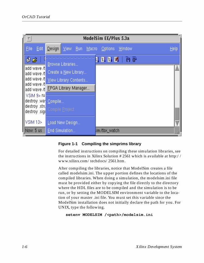
This tutorial uses the simprims library for XC9500/XL/XV designs. To compile the simprims library, invoke ModelSim by entering
vsim &
Design -> FPGA Library Manager -> Vendor File selection
Open fpgavendor_xilinx.tcl in the dialog box.
Compile the simprims library.
OrCAD Tutorial 1-5
OrCAD Tutorial
Figure 1-1 Compiling the simprims library
For detailed instructions on compiling these simulation libraries, see the instructions in Xilinx Solution # 2561 which is available at http://www.xilinx.com/techdocs/2561.htm.
After compiling the libraries, notice that ModelSim creates a file called modelsim.ini. The upper portion defines the locations of the compiled libraries. When doing a simulation, the modelsim.ini file must be provided either by copying the file directly to the directory where the HDL files are to be compiled and the simulation is to be run, or by setting the MODELSIM environment variable to the loca-tion of your master .ini file. You must set this variable since the ModelSim installation does not initially declare the path for you. For UNIX, type the following.
setenv MODELSIM /<path>/modelsim.ini
1-6 Xilinx Development System
OrCAD/ModelSim Tutorial for CPLDs
RTL SimulationFunctional simulation is the same for the XC9500/XL/XV and XCR devices. In this tutorial, no simulation library is used for functional simulation. This note focuses on using the ModelSim simulator. The ModelSim/XE is supports VHDL simulation. Express provides a simulator which can be used. For small design, Xilinx provides the easy to use XSim simulation utility.
Starting ModelSimIf you are using the PC, invoke the simulator by selecting Programs → Model Tech → ModelSim from the Start menu. For UNIX work-stations, type the following at the prompt.
vsim -i &
Set the project directory using the File → Change Directory menu command.
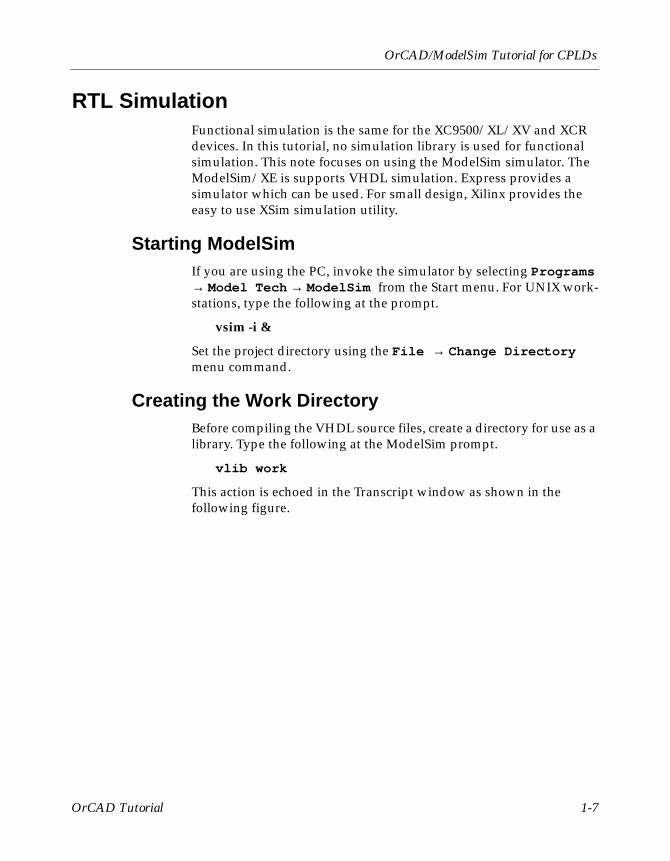
Creating the Work DirectoryBefore compiling the VHDL source files, create a directory for use as a library. Type the following at the ModelSim prompt.
vlib work
This action is echoed in the Transcript window as shown in the following figure.
OrCAD Tutorial 1-7
OrCAD Tutorial
Figure 1-2 MTI Transcript Window
Compiling the Source Files
VHDL
The vcom command compiles VHDL code for use with Vsim RTL simulation. Also, to enhance simulation, both Express and ModelSim support VHDL ‘93. The -93 switch is used to enable support for 1076-93. Type the following at the ModelSim prompt.
vcom -93 -explicit smallcntr.vhd
vcom -93 divider.vhd cnt60.vhd tenths.vhd
vcom -93 hex2led.vhd stmchine.vhd
vcom -93 watch.vhd testbench.vhd
The -explicit is used to compile smallcntr.vhd since there is a defini-tion of “=” in the std_logic_1164 and std_logic_unsigned libraries that are declared for the entity. The option resolves resolution conflicts in favor of explicit function.
1-8 Xilinx Development System
OrCAD/ModelSim Tutorial for CPLDs
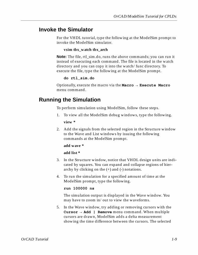
Invoke the SimulatorFor the VHDL tutorial, type the following at the ModelSim prompt to invoke the ModelSim simulator.
vsim tbx_watch tbx_arch
Note: The file, rtl_sim.do, runs the above commands; you can run it instead of executing each command. The file is located in the watch directory and you can copy it into the watch/func directory. To execute the file, type the following at the ModelSim prompt.
do rtl_sim.do
Optionally, execute the macro via the Macro → Execute Macro menu command.
Running the SimulationTo perform simulation using ModelSim, follow these steps.
1. To view all the ModelSim debug windows, type the following.
view *
2. Add the signals from the selected region in the Structure window to the Wave and List windows by issuing the following commands at the ModelSim prompt.
add wave *
add list *
3. In the Structure window, notice that VHDL design units are indi-cated by squares. You can expand and collapse regions of hier-archy by clicking on the (+) and (-) notations.
4. To run the simulation for a specified amount of time at the ModelSim prompt, type the following.
run 100000 ns
The simulation output is displayed in the Wave window. You may have to zoom in/out to view the waveforms.
5. In the Wave window, try adding or removing cursors with the Cursor → Add | Remove menu command. When multiple cursors are drawn, ModelSim adds a delta measurement showing the time difference between the cursors. The selected
OrCAD Tutorial 1-9
OrCAD Tutorial
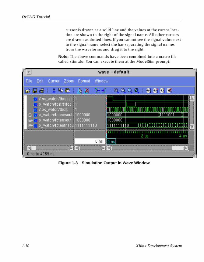
cursor is drawn as a solid line and the values at the cursor loca-tion are shown to the right of the signal name. All other cursors are drawn as dotted lines. If you cannot see the signal value next to the signal name, select the bar separating the signal names from the waveforms and drag it to the right.
Note: The above commands have been combined into a macro file called stim.do. You can execute them at the ModelSim prompt.
Figure 1-3 Simulation Output in Wave Window
1-10 Xilinx Development System
OrCAD/ModelSim Tutorial for CPLDs
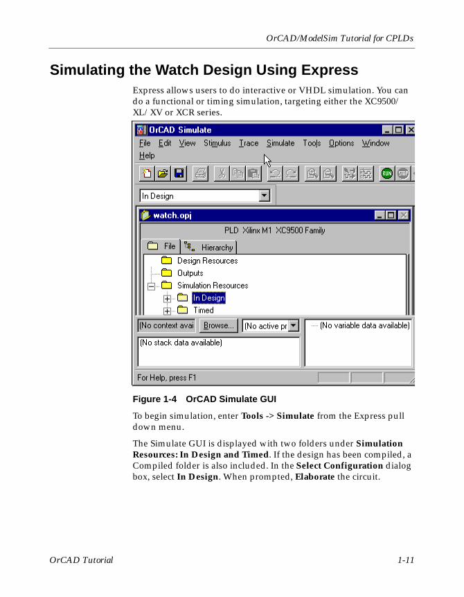
Simulating the Watch Design Using ExpressExpress allows users to do interactive or VHDL simulation. You can do a functional or timing simulation, targeting either the XC9500/XL/XV or XCR series.
Figure 1-4 OrCAD Simulate GUI
To begin simulation, enter Tools -> Simulate from the Express pull down menu.
The Simulate GUI is displayed with two folders under Simulation Resources: In Design and Timed. If the design has been compiled, a Compiled folder is also included. In the Select Configuration dialog box, select In Design. When prompted, Elaborate the circuit.
OrCAD Tutorial 1-11
OrCAD Tutorial
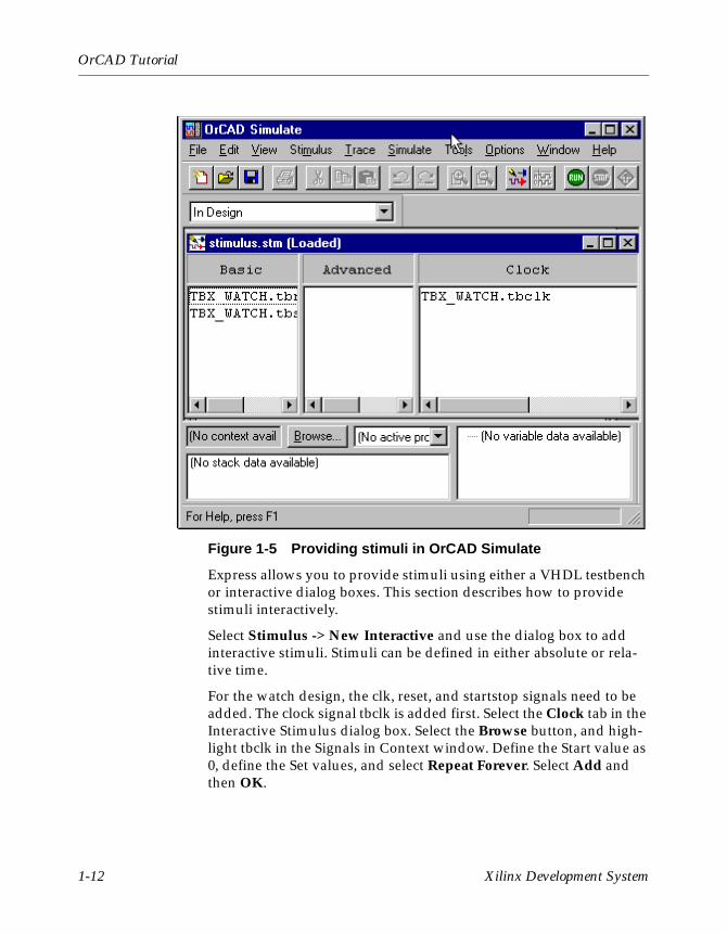
Figure 1-5 Providing stimuli in OrCAD Simulate
Express allows you to provide stimuli using either a VHDL testbench or interactive dialog boxes. This section describes how to provide stimuli interactively.
Select Stimulus -> New Interactive and use the dialog box to add interactive stimuli. Stimuli can be defined in either absolute or rela-tive time.
For the watch design, the clk, reset, and startstop signals need to be added. The clock signal tbclk is added first. Select the Clock tab in the Interactive Stimulus dialog box. Select the Browse button, and high-light tbclk in the Signals in Context window. Define the Start value as 0, define the Set values, and select Repeat Forever. Select Add and then OK.
1-12 Xilinx Development System
OrCAD/ModelSim Tutorial for CPLDs
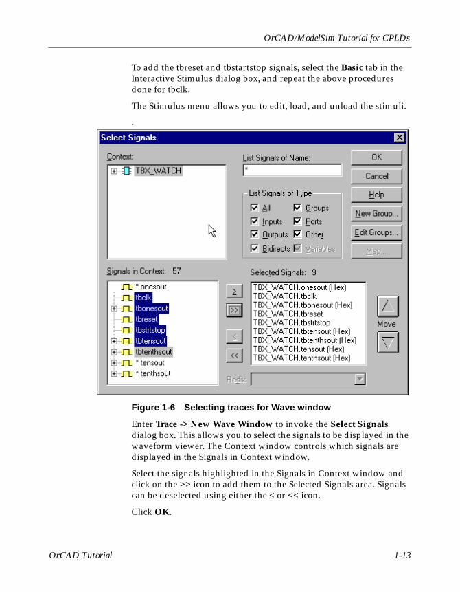
To add the tbreset and tbstartstop signals, select the Basic tab in the Interactive Stimulus dialog box, and repeat the above procedures done for tbclk.
The Stimulus menu allows you to edit, load, and unload the stimuli.
.
Figure 1-6 Selecting traces for Wave window
Enter Trace -> New Wave Window to invoke the Select Signals dialog box. This allows you to select the signals to be displayed in the waveform viewer. The Context window controls which signals are displayed in the Signals in Context window.
Select the signals highlighted in the Signals in Context window and click on the >> icon to add them to the Selected Signals area. Signals can be deselected using either the < or << icon.
Click OK.
OrCAD Tutorial 1-13
OrCAD Tutorial
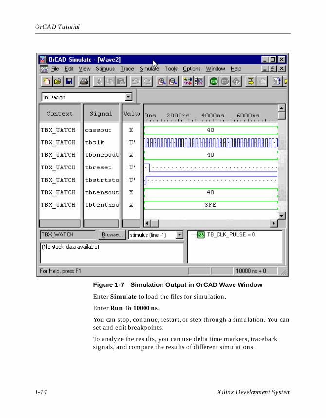
Figure 1-7 Simulation Output in OrCAD Wave Window
Enter Simulate to load the files for simulation.
Enter Run To 10000 ns.
You can stop, continue, restart, or step through a simulation. You can set and edit breakpoints.
To analyze the results, you can use delta time markers, traceback signals, and compare the results of different simulations.
1-14 Xilinx Development System
OrCAD/ModelSim Tutorial for CPLDs
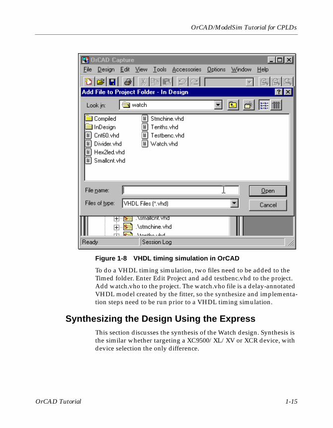
Figure 1-8 VHDL timing simulation in OrCAD
To do a VHDL timing simulation, two files need to be added to the Timed folder. Enter Edit Project and add testbenc.vhd to the project. Add watch.vho to the project. The watch.vho file is a delay-annotated VHDL model created by the fitter, so the synthesize and implementa-tion steps need to be run prior to a VHDL timing simulation.
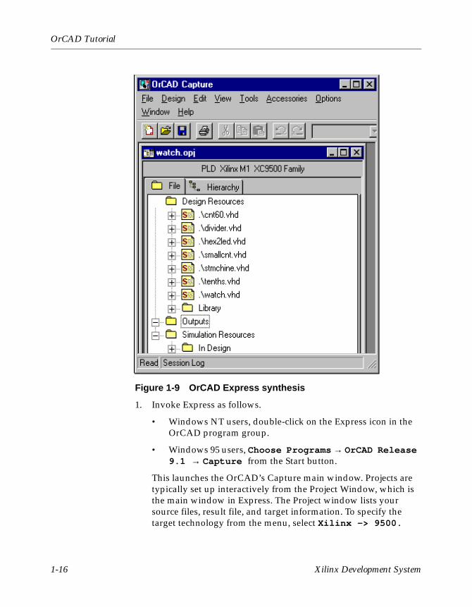
Synthesizing the Design Using the ExpressThis section discusses the synthesis of the Watch design. Synthesis is the similar whether targeting a XC9500/XL/XV or XCR device, with device selection the only difference.
OrCAD Tutorial 1-15
OrCAD Tutorial
Figure 1-9 OrCAD Express synthesis
1. Invoke Express as follows.
• Windows NT users, double-click on the Express icon in the OrCAD program group.
• Windows 95 users, Choose Programs → OrCAD Release 9.1 → Capture from the Start button.
This launches the OrCAD’s Capture main window. Projects are typically set up interactively from the Project Window, which is the main window in Express. The Project window lists your source files, result file, and target information. To specify the target technology from the menu, select Xilinx -> 9500.
1-16 Xilinx Development System
OrCAD/ModelSim Tutorial for CPLDs
2. Open a new project with the File → New Project menu.
3. If you are going to download this design to the demoboard, choose the XCR3256 in the 144 TQFP. 1831G
4. The Design Resources area of the Express main window is where you specify input design files. To specify your input files, select Edit Project and add the files.
5. For the VHDL tutorial, change the order of the VHDL input source files to the following order.
smallcntr.vhd
divider.vhd
cnt60.vhd
hex2led.vhd
stmchine.vhd
watch.vhd
6. The pinout is defined in the .ucf file in the implementation phase. It is highly recommended that you let the fitter define the pinout. Pre-assigning locations to the I/Os can degrade the performance of the fitter. However, it is usually necessary, at some point, to lock the pinout of a design so that it can be integrated into a board design. The initial pinout should be defined by running the fitter without pin assignments, then locking down the I/O place-ment so that it reflects the locations chosen by the tools. As a general rule, inputs should be placed on the left side of the die, and outputs on the right. The I/O in this tutorial must be assigned pin locations only if the Watch design is used in the XCR demo board. Since the design is fairly simple, these pin assignments do not adversely affect the ability of the fitter to fit the design completely.
Note: Pin assignments can also made directly into the HDL. Please read Xilinx Solution # 2379 which is available at http://www.xilinx.com/techdocs/2379.htm for instructions.
7. To lock the RESET and STRTSTOP signals, edit the partially completed SDC file, watch.sdc, that is provided for you. Add the following lines.
define_attribute RESET xc_loc “<pin_location>”
OrCAD Tutorial 1-17
OrCAD Tutorial
define_attribute STRTSTOP xc_loc “<pin_location>”
since Express automatically recognizes and extracts the state machines in the design, and performs the Symbolic FSM Compiler optimizations.
8. To synthesize the design, select Tools -> Compile.
If Express reports only warnings, and no errors, it does complete the mapping to your target device. Nevertheless, it is important to investigate any warnings messages from Express, before continuing your design process.
9. When synthesis is done, Express creates the .edf and .sum files with the filename specified in the user interface.
Double-click the left mouse button on the result filename to see it displayed in the Editing Window.
1-18 Xilinx Development System
OrCAD/ModelSim Tutorial for CPLDs
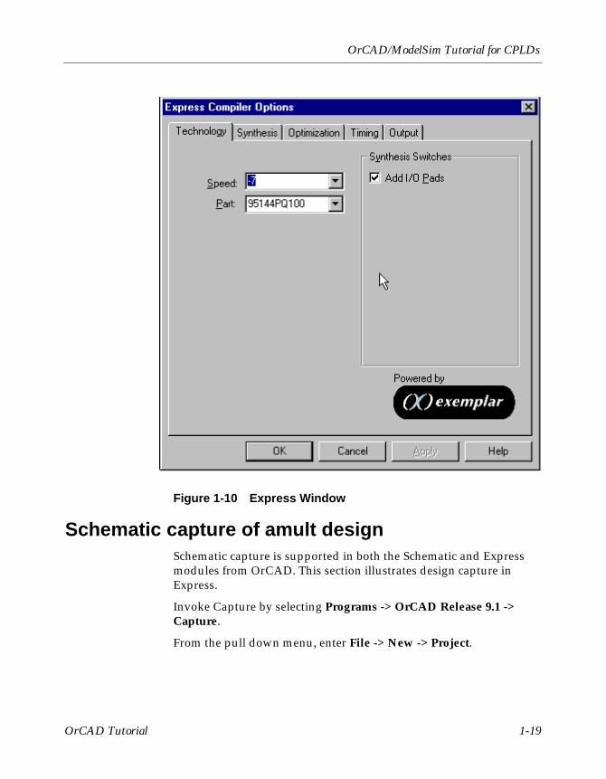
Figure 1-10 Express Window
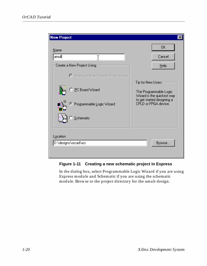
Schematic capture of amult designSchematic capture is supported in both the Schematic and Express modules from OrCAD. This section illustrates design capture in Express.
Invoke Capture by selecting Programs -> OrCAD Release 9.1 -> Capture.
From the pull down menu, enter File -> New -> Project.
OrCAD Tutorial 1-19
OrCAD Tutorial
Figure 1-11 Creating a new schematic project in Express
In the dialog box, select Programmable Logic Wizard if you are using Express module and Schematic if you are using the schematic module. Browse to the project directory for the amult design.
1-20 Xilinx Development System
OrCAD/ModelSim Tutorial for CPLDs
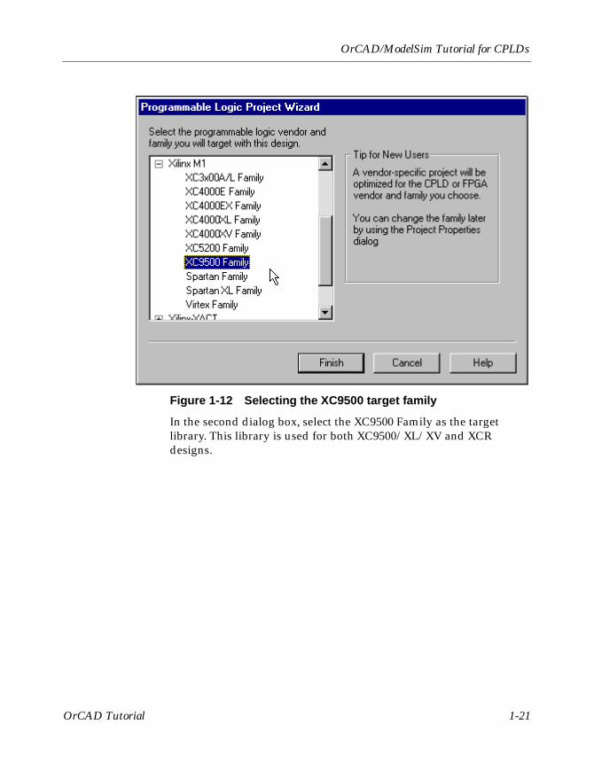
Figure 1-12 Selecting the XC9500 target family
In the second dialog box, select the XC9500 Family as the target library. This library is used for both XC9500/XL/XV and XCR designs.
OrCAD Tutorial 1-21
OrCAD Tutorial
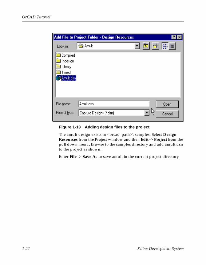
Figure 1-13 Adding design files to the project
The amult design exists in <orcad_path>\samples. Select Design Resources from the Project window and then Edit -> Project from the pull down menu. Browse to the samples directory and add amult.dsn to the project as shown.
Enter File -> Save As to save amult in the current project directory.
1-22 Xilinx Development System
OrCAD/ModelSim Tutorial for CPLDs
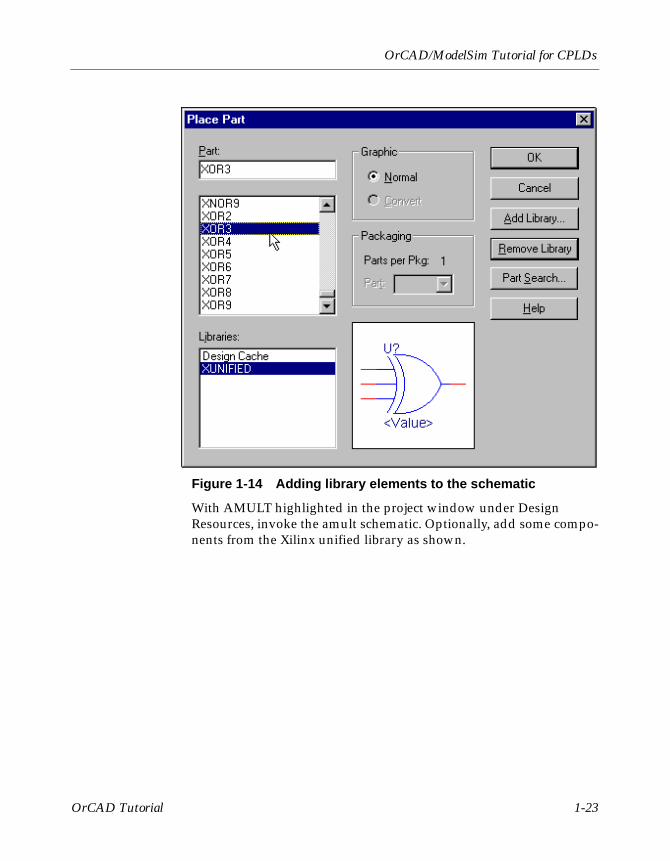
Figure 1-14 Adding library elements to the schematic
With AMULT highlighted in the project window under Design Resources, invoke the amult schematic. Optionally, add some compo-nents from the Xilinx unified library as shown.
OrCAD Tutorial 1-23
OrCAD Tutorial
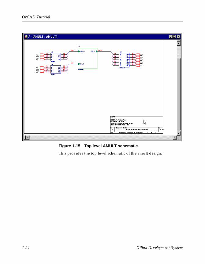
Figure 1-15 Top level AMULT schematic
This provides the top level schematic of the amult design.
1-24 Xilinx Development System
OrCAD/ModelSim Tutorial for CPLDs
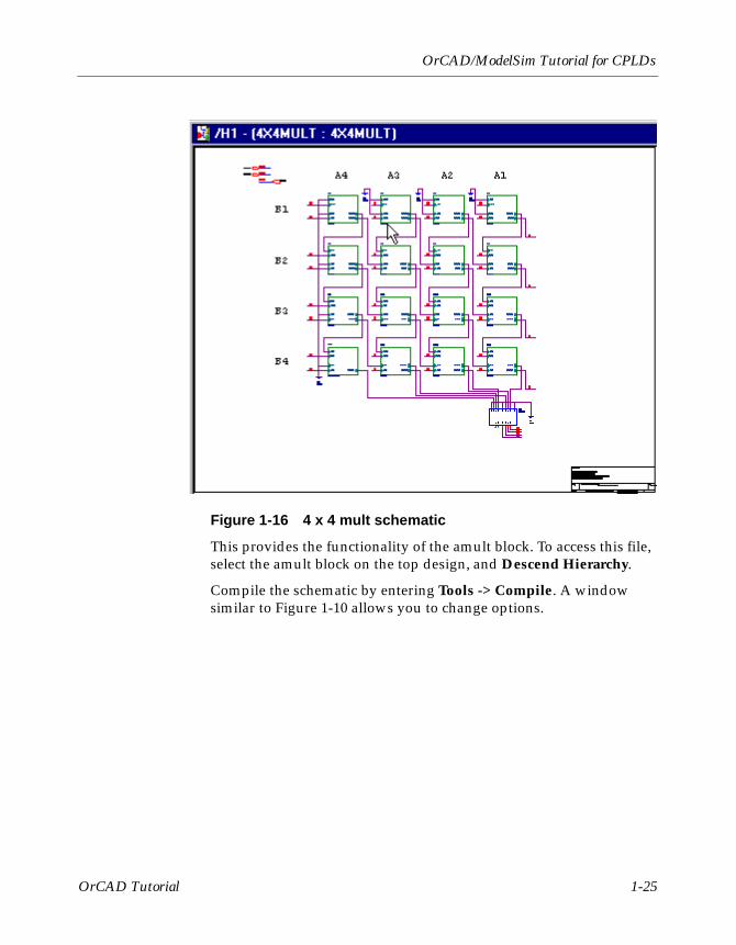
Figure 1-16 4 x 4 mult schematic
This provides the functionality of the amult block. To access this file, select the amult block on the top design, and Descend Hierarchy.
Compile the schematic by entering Tools -> Compile. A window similar to Figure 1-10 allows you to change options.
OrCAD Tutorial 1-25
OrCAD Tutorial
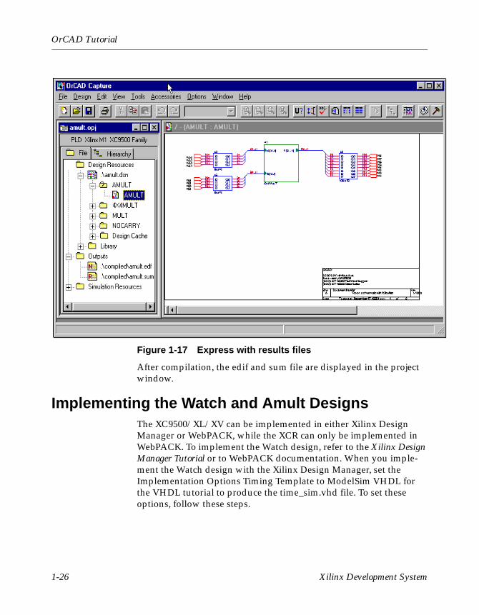
Figure 1-17 Express with results files
After compilation, the edif and sum file are displayed in the project window.
Implementing the Watch and Amult DesignsThe XC9500/XL/XV can be implemented in either Xilinx Design Manager or WebPACK, while the XCR can only be implemented in WebPACK. To implement the Watch design, refer to the Xilinx Design Manager Tutorial or to WebPACK documentation. When you imple-ment the Watch design with the Xilinx Design Manager, set the Implementation Options Timing Template to ModelSim VHDL for the VHDL tutorial to produce the time_sim.vhd file. To set these options, follow these steps.
1-26 Xilinx Development System
OrCAD/ModelSim Tutorial for CPLDs
1. In the Design Manger’s Implement window, select Options under the Design pull-down menu, to open the Options dialog box.
2. In the Program Option Template, set Simulation to ModelSim VHDL for the VHDL tutorial.
3. Proceed with the Design Manager or WebPACK tutorial.
Note: Although not included in this tutorial, it is possible to run a post-Ngdbuild and post-Map simulation, which may be helpful for debugging the design.
XC9500/XL/XV Timing SimulationFor VHDL simulation, you need two files.
• time_sim.vhd
• time_sim.sdf
To perform timing simulation, follow these steps.
1. Copy time_sim.vhd, time_sim.sdf, and testbench.vhd to the simulation directory.
2. Launch ModelSim, and navigate to the simulation directory.
3. Create the work directory.
vlib work
4. Compile the VHDL source files and the testbench.
vcom time_sim.vhd testbench.vhd
5. Read in the SDF file for timing simulation.
vsim -sdftyp uut=time_sim.sdf tbx_watch tbx_arch
Alternatively, select File → Load New Design. Highlight the design in the Design Unit window. Click the Add button. To apply the timing data, click on the SDF tab on the Load Design window. Click the Add button. Browse and select the time_sim.sdf file. Type uut in the Apply to Region field and click the Load button.
6. View the necessary debugging windows by typing the following command at the ModelSim prompt.
OrCAD Tutorial 1-27
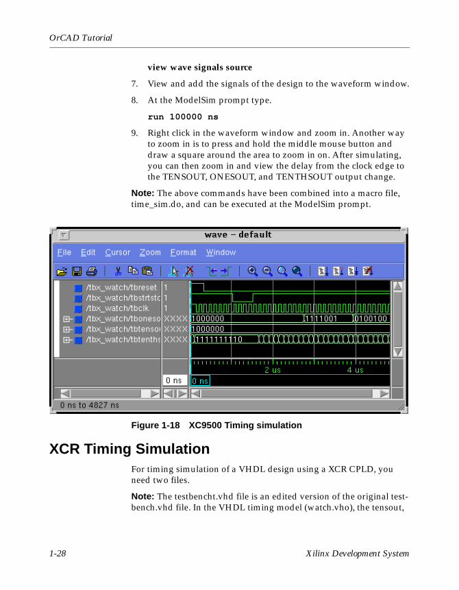
OrCAD Tutorial
view wave signals source
7. View and add the signals of the design to the waveform window.
8. At the ModelSim prompt type.
run 100000 ns
9. Right click in the waveform window and zoom in. Another way to zoom in is to press and hold the middle mouse button and draw a square around the area to zoom in on. After simulating, you can then zoom in and view the delay from the clock edge to the TENSOUT, ONESOUT, and TENTHSOUT output change.
Note: The above commands have been combined into a macro file, time_sim.do, and can be executed at the ModelSim prompt.
Figure 1-18 XC9500 Timing simulation
XCR Timing SimulationFor timing simulation of a VHDL design using a XCR CPLD, you need two files.
Note: The testbencht.vhd file is an edited version of the original test-bench.vhd file. In the VHDL timing model (watch.vho), the tensout,
1-28 Xilinx Development System
OrCAD/ModelSim Tutorial for CPLDs
onesout, and tenthsout bus signals are broken into discrete signals. For simulation, the component signals and uut signals in the test-bench and design model must match. The component and uut instan-tiation statements in testbencht.vhd have been edited to match those in watch.vho.
• watch.vho
• testbencht.vhd
To perform timing simulation, follow these steps.
1. Copy watch.vho and testbencht.vhd to the simulation directory.
2. Launch ModelSim, and navigate to the simulation directory.
3. Create the work directory.
vlib work
4. Compile the VHDL source files and the testbench.
vcom watch.vho testbencht.vhd
5. Read in the files for timing simulation.
vsim tbx_watch tbx_arch
Alternatively, select File → Load New Design. Click the Add button. Browse and select the design file. Type uut in the Apply to Region field and click the Load button.
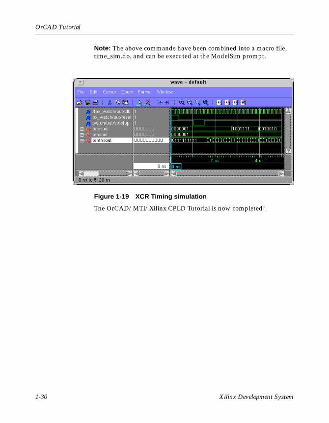
6. View the necessary debugging windows by typing the following command at the ModelSim prompt.
view wave signals source
7. View and add the signals of the design to the waveform window. Use the ModelSim Combine command to group the tensout and onesout signals into buses.
8. At the ModelSim prompt type.
run 100000 ns
9. Right click in the waveform window and zoom in. Another way to zoom in, press and hold the middle mouse button and draw a square around the area to zoom in on. After simulating, you can then zoom in and view the delay from the clock edge to the TENSOUT, ONESOUT, and TENTHSOUT output change.
OrCAD Tutorial 1-29
OrCAD Tutorial
Note: The above commands have been combined into a macro file, time_sim.do, and can be executed at the ModelSim prompt.
Figure 1-19 XCR Timing simulation
The OrCAD/MTI/Xilinx CPLD Tutorial is now completed!
1-30 Xilinx Development System