Embed Size (px)
Citation preview

1
OrCAD PSPICE Tutorial
OrCAD Release 9.2, Capture Lite Edition, PSpice AD Lite Edition
Part 0: Some General PSpice Guidelines
1. All component leads must be connected. Floating leads will result in an error.
2. All circuits must have a zero, “0”, reference ground node as shown below.
0 3. PSpice syntax is case insensitive, thus, PSpice will interpret a resistor component
reference “r1” the same as “R1”; “k” (for kilo) the same as “K”; etc.
4. Component values may be designated with the following suffixes:
k, K = 103 “kilo”
m, M = 10-3 “milli” [Note: Since PSpice is case insensitive,
meg, MEG = 106 “mega” “M”, designates “milli” not “mega”]
u, U = 10-6 “micro”
g, G = 109 “giga”
n, N = 10-9 “nano”
t, T = 1012 “tera”
p, P = 10-12 “pico”
5. Do not leave a space between a number and it’s suffix, i.e. a resistor value of
1000 Ω can be designated as “1k”, not “1 k”.
6. Each instance of a component must be assigned a unique reference, i.e. there may
only be one resistor labeled “R1” in a circuit.
7. If a PSpice simulation fails due to an error, check the session log or view the
output file to determine which node(s) are associated with the error. Then look at
the netlist to determine which component(s) are connected to the node(s) where
the problem exits.
2
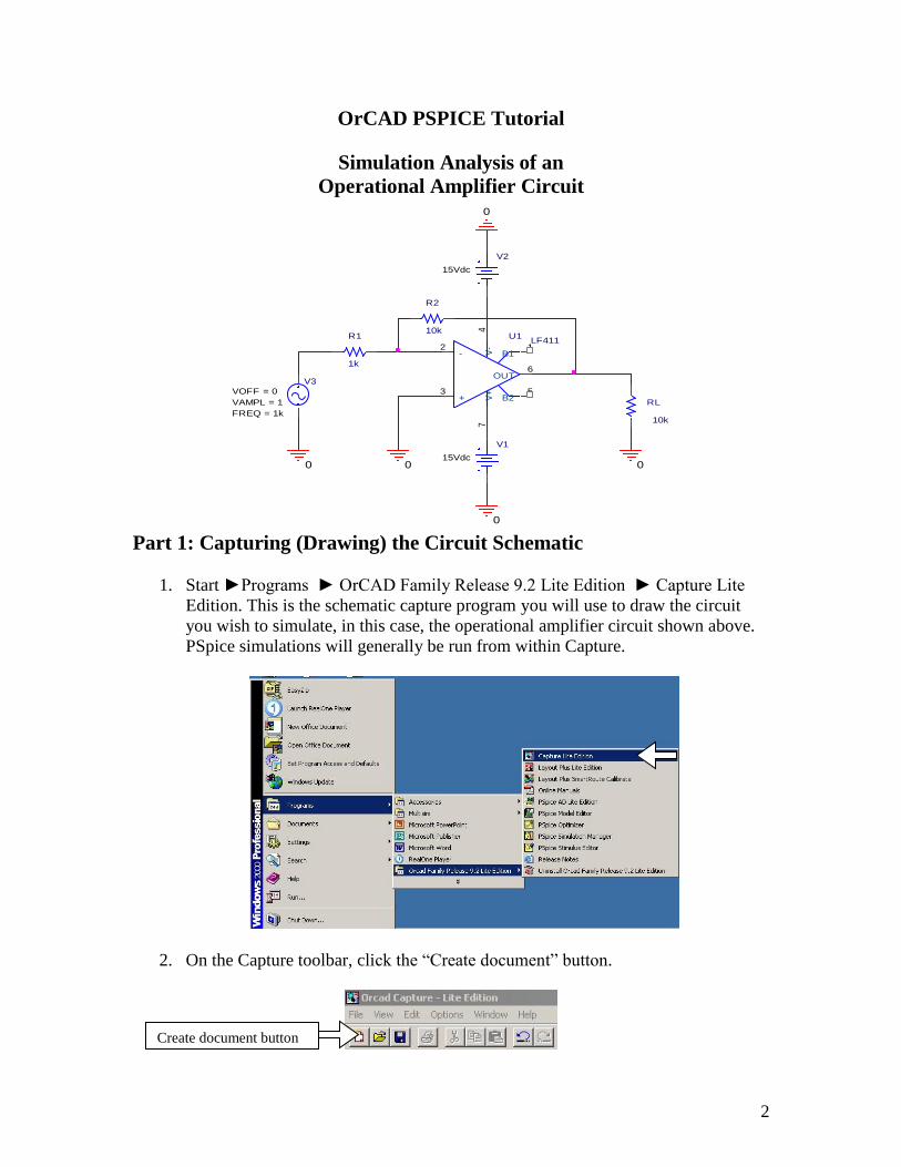
OrCAD PSPICE Tutorial
Simulation Analysis of an
Operational Amplifier Circuit
V3
FREQ = 1k
VAMPL = 1
VOFF = 0
0
0
U1LF411
3
2
74
6
1
5+
-
V+
V-
OUT
B1
B2
R2
10k
0
V2
15Vdc
0
0
R1
1k
RL
10k
V1
15Vdc
Part 1: Capturing (Drawing) the Circuit Schematic
1. Start ►Programs ► OrCAD Family Release 9.2 Lite Edition ► Capture Lite
Edition. This is the schematic capture program you will use to draw the circuit
you wish to simulate, in this case, the operational amplifier circuit shown above.
PSpice simulations will generally be run from within Capture.
2. On the Capture toolbar, click the “Create document” button.
Create document button
3
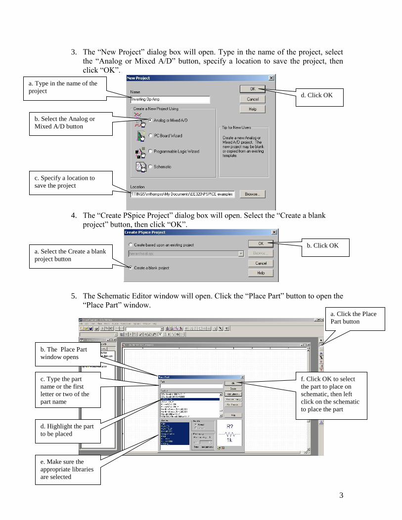
3. The “New Project” dialog box will open. Type in the name of the project, select
the “Analog or Mixed A/D” button, specify a location to save the project, then
click “OK”.
4. The “Create PSpice Project” dialog box will open. Select the “Create a blank
project” button, then click “OK”.
5. The Schematic Editor window will open. Click the “Place Part” button to open the
“Place Part” window.
a. Type in the name of the
project
b. Select the Analog or
Mixed A/D button
c. Specify a location to
save the project
d. Click OK
a. Select the Create a blank
project button
b. Click OK
a. Click the Place
Part button
b. The Place Part
window opens
c. Type the part
name or the first
letter or two of the
part name
d. Highlight the part
to be placed
e. Make sure the
appropriate libraries
are selected
f. Click OK to select
the part to place on
schematic, then left
click on the schematic
to place the part
4
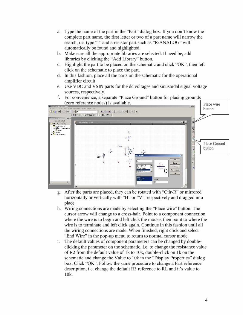
a. Type the name of the part in the “Part” dialog box. If you don’t know the
complete part name, the first letter or two of a part name will narrow the
search, i.e. type “r” and a resistor part such as “R/ANALOG” will
automatically be found and highlighted.
b. Make sure all the appropriate libraries are selected. If need be, add
libraries by clicking the “Add Library” button.
c. Highlight the part to be placed on the schematic and click “OK”, then left
click on the schematic to place the part.
d. In this fashion, place all the parts on the schematic for the operational
amplifier circuit.
e. Use VDC and VSIN parts for the dc voltages and sinusoidal signal voltage
sources, respectively.
f. For convenience, a separate “Place Ground” button for placing grounds
(zero reference nodes) is available.
g. After the parts are placed, they can be rotated with “Ctlr-R” or mirrored
horizontally or vertically with “H” or “V”, respectively and dragged into
place.
h. Wiring connections are made by selecting the “Place wire” button. The
cursor arrow will change to a cross-hair. Point to a component connection
where the wire is to begin and left click the mouse, then point to where the
wire is to terminate and left click again. Continue in this fashion until all
the wiring connections are made. When finished, right click and select
“End Wire” in the pop-up menu to return to normal cursor mode.
i. The default values of component parameters can be changed by double-
clicking the parameter on the schematic, i.e. to change the resistance value
of R2 from the default value of 1k to 10k, double-click on 1k on the
schematic and change the Value to 10k in the “Display Properties” dialog
box. Click “OK”. Follow the same procedure to change a Part reference
description, i.e. change the default R3 reference to RL and it’s value to
10k.
Place Ground
button
Place wire
button
5
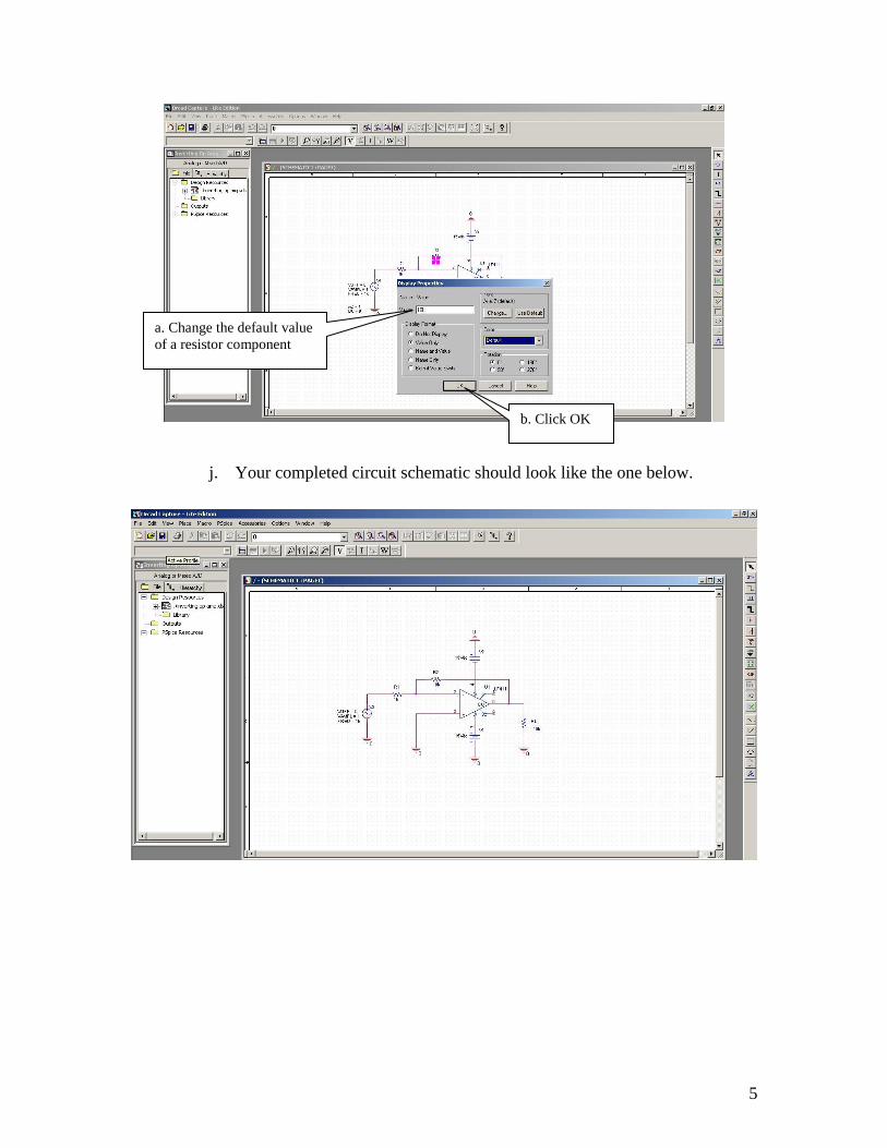
j. Your completed circuit schematic should look like the one below.
a. Change the default value
of a resistor component
b. Click OK
6
OrCAD PSPICE Tutorial
Part 2: DC Bias Point Analysis
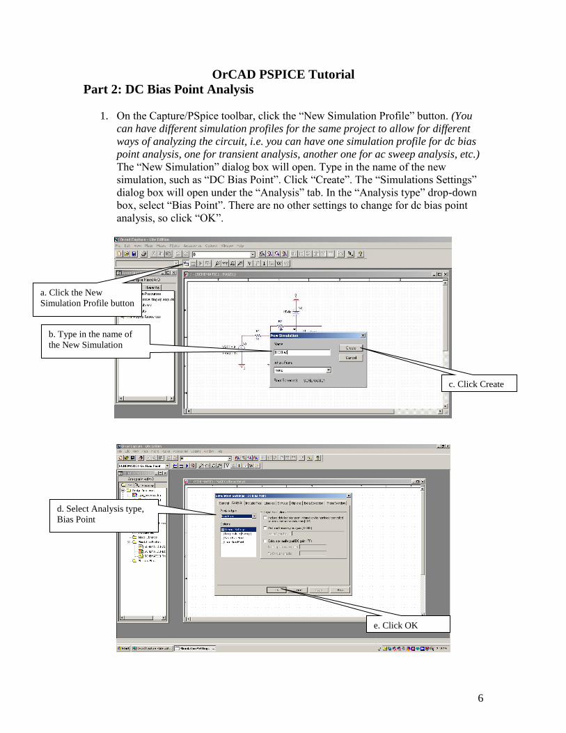
1. On the Capture/PSpice toolbar, click the “New Simulation Profile” button. (You
can have different simulation profiles for the same project to allow for different
ways of analyzing the circuit, i.e. you can have one simulation profile for dc bias
point analysis, one for transient analysis, another one for ac sweep analysis, etc.)
The “New Simulation” dialog box will open. Type in the name of the new
simulation, such as “DC Bias Point”. Click “Create”. The “Simulations Settings”
dialog box will open under the “Analysis” tab. In the “Analysis type” drop-down
box, select “Bias Point”. There are no other settings to change for dc bias point
analysis, so click “OK”.
a. Click the New
Simulation Profile button
b. Type in the name of
the New Simulation
c. Click Create
d. Select Analysis type,
Bias Point
e. Click OK
7
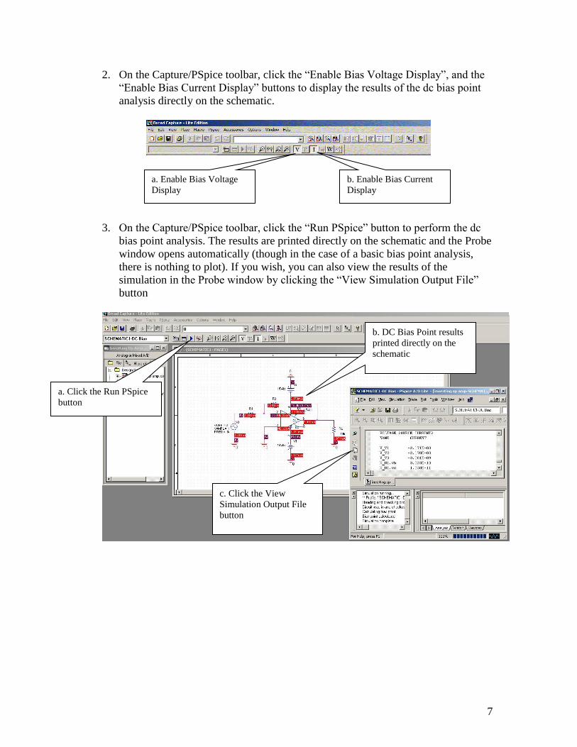
2. On the Capture/PSpice toolbar, click the “Enable Bias Voltage Display”, and the
“Enable Bias Current Display” buttons to display the results of the dc bias point
analysis directly on the schematic.
3. On the Capture/PSpice toolbar, click the “Run PSpice” button to perform the dc
bias point analysis. The results are printed directly on the schematic and the Probe
window opens automatically (though in the case of a basic bias point analysis,
there is nothing to plot). If you wish, you can also view the results of the
simulation in the Probe window by clicking the “View Simulation Output File”
button
a. Enable Bias Voltage
Display
b. Enable Bias Current
Display
a. Click the Run PSpice
button
c. Click the View
Simulation Output File
button
b. DC Bias Point results
printed directly on the
schematic
8
OrCAD PSPICE Tutorial
Part 3: Transient Analysis
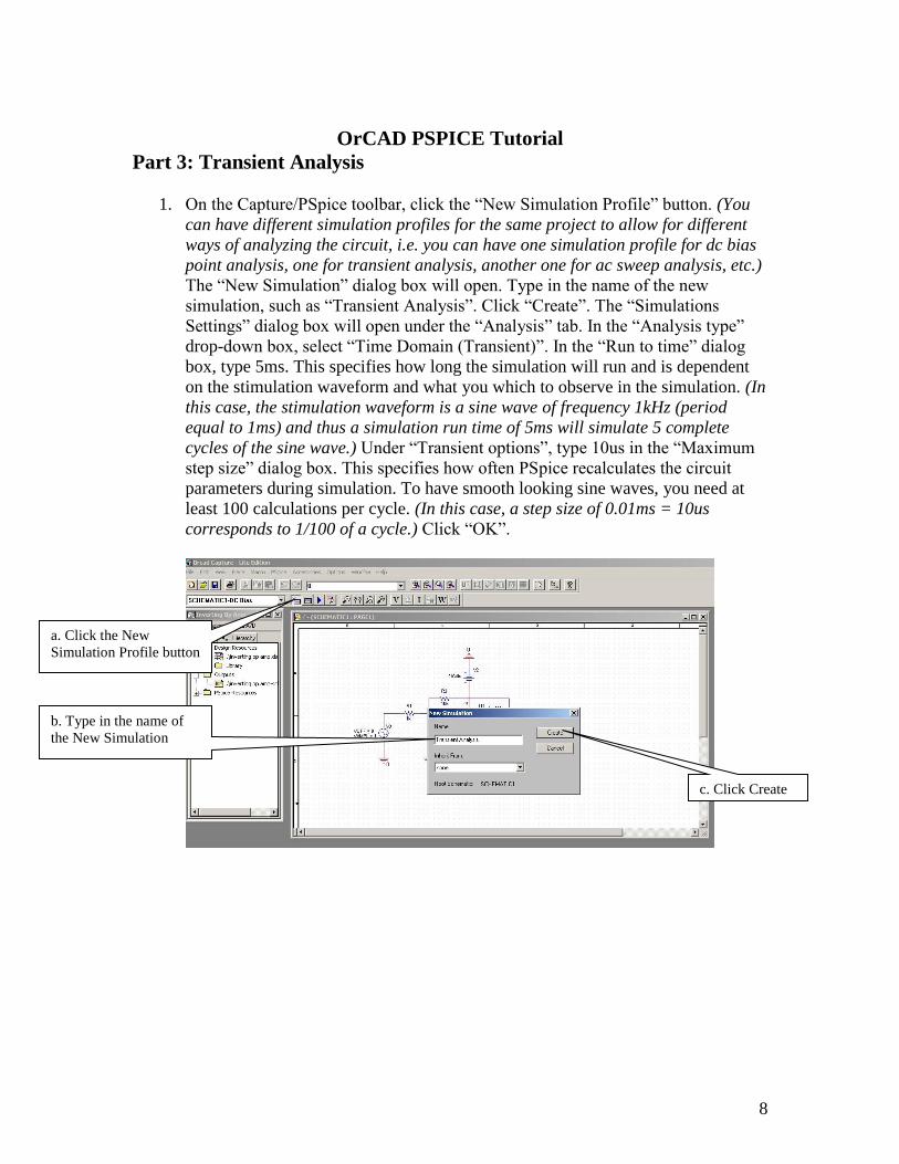
1. On the Capture/PSpice toolbar, click the “New Simulation Profile” button. (You
can have different simulation profiles for the same project to allow for different
ways of analyzing the circuit, i.e. you can have one simulation profile for dc bias
point analysis, one for transient analysis, another one for ac sweep analysis, etc.)
The “New Simulation” dialog box will open. Type in the name of the new
simulation, such as “Transient Analysis”. Click “Create”. The “Simulations
Settings” dialog box will open under the “Analysis” tab. In the “Analysis type”
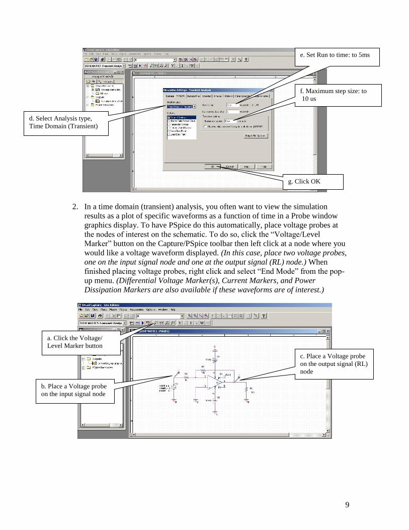
drop-down box, select “Time Domain (Transient)”. In the “Run to time” dialog
box, type 5ms. This specifies how long the simulation will run and is dependent
on the stimulation waveform and what you which to observe in the simulation. (In
this case, the stimulation waveform is a sine wave of frequency 1kHz (period
equal to 1ms) and thus a simulation run time of 5ms will simulate 5 complete
cycles of the sine wave.) Under “Transient options”, type 10us in the “Maximum
step size” dialog box. This specifies how often PSpice recalculates the circuit
parameters during simulation. To have smooth looking sine waves, you need at
least 100 calculations per cycle. (In this case, a step size of 0.01ms = 10us
corresponds to 1/100 of a cycle.) Click “OK”.
a. Click the New
Simulation Profile button
b. Type in the name of
the New Simulation
c. Click Create
9
2. In a time domain (transient) analysis, you often want to view the simulation
results as a plot of specific waveforms as a function of time in a Probe window
graphics display. To have PSpice do this automatically, place voltage probes at
the nodes of interest on the schematic. To do so, click the “Voltage/Level
Marker” button on the Capture/PSpice toolbar then left click at a node where you
would like a voltage waveform displayed. (In this case, place two voltage probes,
one on the input signal node and one at the output signal (RL) node.) When
finished placing voltage probes, right click and select “End Mode” from the pop-
up menu. (Differential Voltage Marker(s), Current Markers, and Power
Dissipation Markers are also available if these waveforms are of interest.)
a. Click the Voltage/
Level Marker button
b. Place a Voltage probe
on the input signal node
c. Place a Voltage probe
on the output signal (RL)
node
d. Select Analysis type,
Time Domain (Transient)
g. Click OK
e. Set Run to time: to 5ms
f. Maximum step size: to
10 us
10
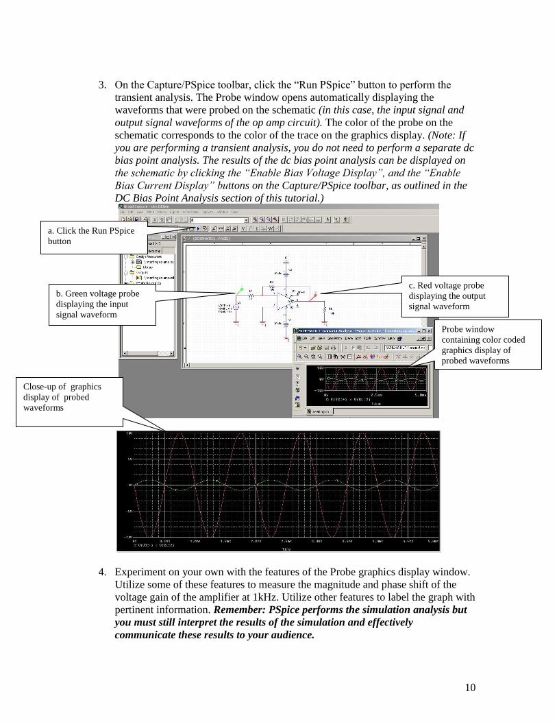
3. On the Capture/PSpice toolbar, click the “Run PSpice” button to perform the
transient analysis. The Probe window opens automatically displaying the
waveforms that were probed on the schematic (in this case, the input signal and
output signal waveforms of the op amp circuit). The color of the probe on the
schematic corresponds to the color of the trace on the graphics display. (Note: If
you are performing a transient analysis, you do not need to perform a separate dc
bias point analysis. The results of the dc bias point analysis can be displayed on
the schematic by clicking the “Enable Bias Voltage Display”, and the “Enable
Bias Current Display” buttons on the Capture/PSpice toolbar, as outlined in the
DC Bias Point Analysis section of this tutorial.)
4. Experiment on your own with the features of the Probe graphics display window.
Utilize some of these features to measure the magnitude and phase shift of the
voltage gain of the amplifier at 1kHz. Utilize other features to label the graph with
pertinent information. Remember: PSpice performs the simulation analysis but
you must still interpret the results of the simulation and effectively
communicate these results to your audience.
a. Click the Run PSpice
button
b. Green voltage probe
displaying the input
signal waveform
c. Red voltage probe
displaying the output
signal waveform
Probe window
containing color coded
graphics display of
probed waveforms
Close-up of graphics
display of probed
waveforms
11
OrCAD PSPICE Tutorial
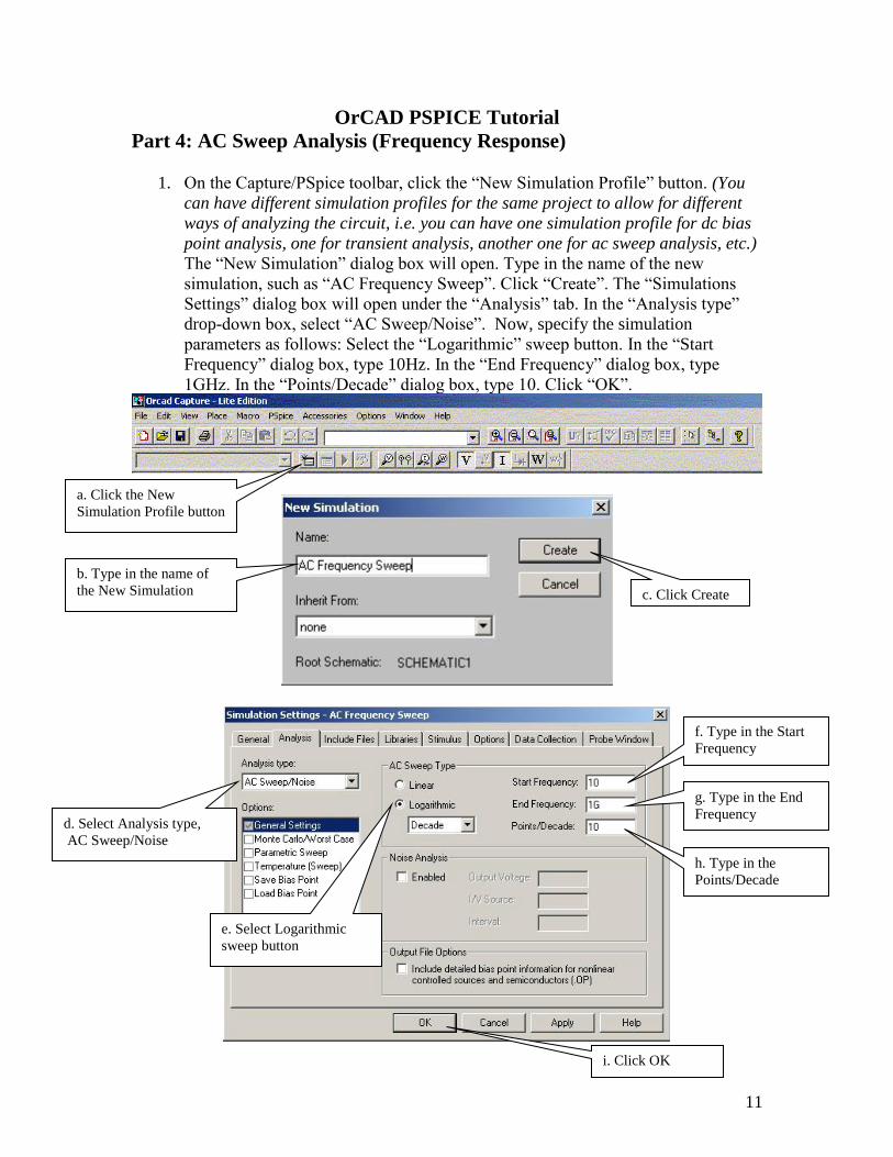
Part 4: AC Sweep Analysis (Frequency Response)
1. On the Capture/PSpice toolbar, click the “New Simulation Profile” button. (You
can have different simulation profiles for the same project to allow for different
ways of analyzing the circuit, i.e. you can have one simulation profile for dc bias
point analysis, one for transient analysis, another one for ac sweep analysis, etc.)
The “New Simulation” dialog box will open. Type in the name of the new
simulation, such as “AC Frequency Sweep”. Click “Create”. The “Simulations
Settings” dialog box will open under the “Analysis” tab. In the “Analysis type”
drop-down box, select “AC Sweep/Noise”. Now, specify the simulation
parameters as follows: Select the “Logarithmic” sweep button. In the “Start
Frequency” dialog box, type 10Hz. In the “End Frequency” dialog box, type
1GHz. In the “Points/Decade” dialog box, type 10. Click “OK”.
a. Click the New
Simulation Profile button
b. Type in the name of
the New Simulation c. Click Create
d. Select Analysis type,
AC Sweep/Noise
e. Select Logarithmic
sweep button
f. Type in the Start
Frequency
g. Type in the End
Frequency
h. Type in the
Points/Decade
i. Click OK

12
2. In a frequency response (ac sweep) analysis, you often want to view the
simulation results as a Bode plot of the gain function in a Probe window graphics
display. To have PSpice do this automatically, we will set the AC magnitude of
the input voltage equal to 1 (a useful analysis trick that makes the output voltage
magnitude equal to the voltage gain magnitude) and place a single voltage probe
at the output node on the schematic. Most time-varying sources also have an AC
magnitude parameter, though it is not usually set to be displayed by default. To
set the small-signal AC magnitude of the time varying source, VSIN, equal to 1
and display it on the schematic, double click on the circuit symbol of V3 on the
schematic to open the “Property Editor” window.
V3
In the “Property Editor” window, highlight the “AC” parameter box and type in
“1” to set the AC magnitude equal to 1, then select the “Display” button to open
the “Display Properties” window. Under “Display Format” in the “Display
Properties” window, select the “Name and Value” button, then click “OK”.
In a similar fashion, set the DC parameter equal to “0” and display it on the
schematic. Next, place a single voltage probe at the output signal (RL) node on the
schematic as you did in the Transient Analysis section of this tutorial.
a. Double click on the circuit symbol on the
schematic to open the Property Editor window
b. Highlight the AC
parameter box and type
in “1”.
c. Select the Display
button.
d. Select the Name
and Value button. e. Click OK
13
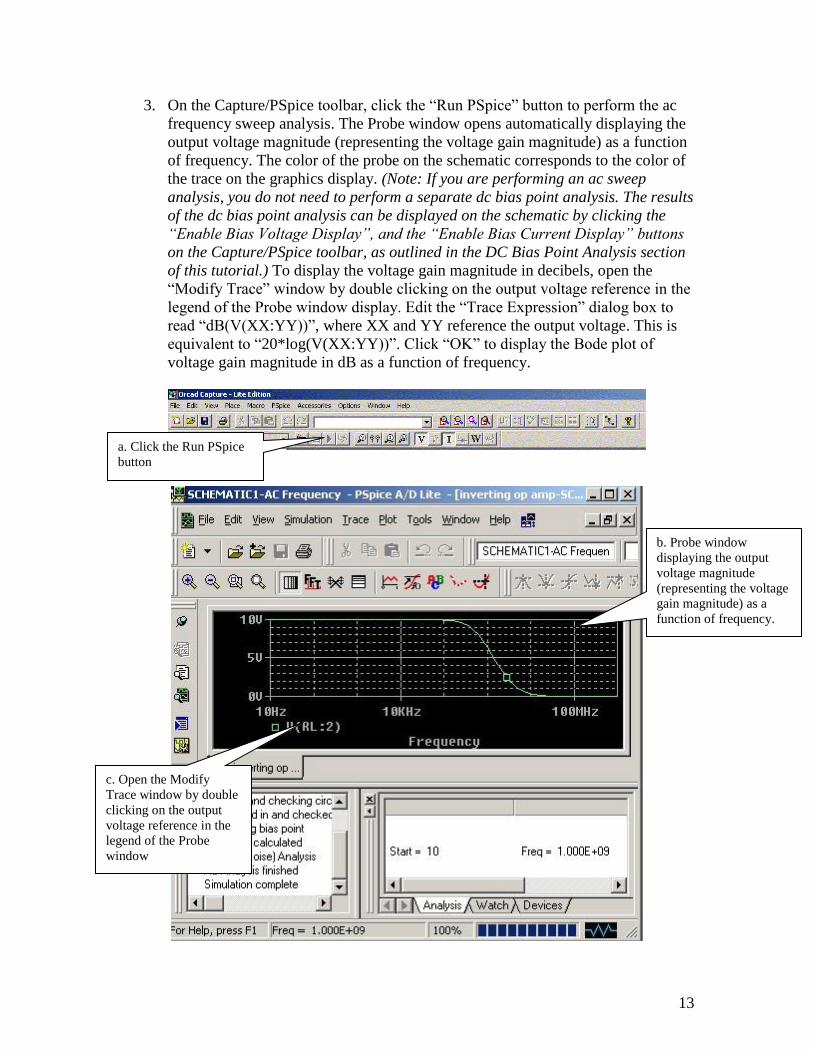
3. On the Capture/PSpice toolbar, click the “Run PSpice” button to perform the ac
frequency sweep analysis. The Probe window opens automatically displaying the
output voltage magnitude (representing the voltage gain magnitude) as a function
of frequency. The color of the probe on the schematic corresponds to the color of
the trace on the graphics display. (Note: If you are performing an ac sweep
analysis, you do not need to perform a separate dc bias point analysis. The results
of the dc bias point analysis can be displayed on the schematic by clicking the
“Enable Bias Voltage Display”, and the “Enable Bias Current Display” buttons
on the Capture/PSpice toolbar, as outlined in the DC Bias Point Analysis section
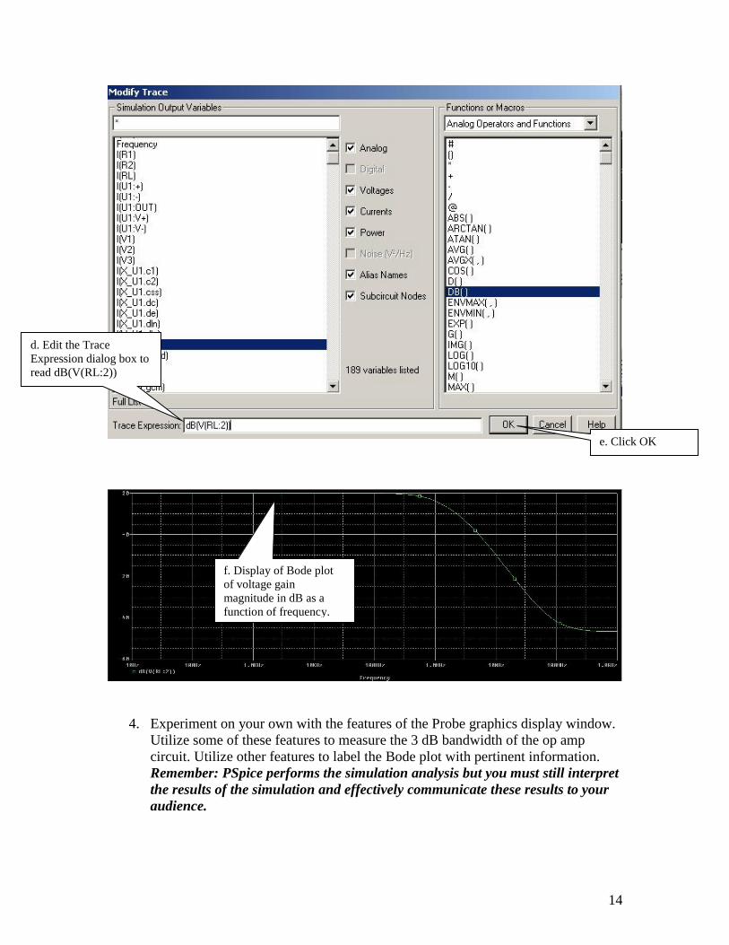
of this tutorial.) To display the voltage gain magnitude in decibels, open the
“Modify Trace” window by double clicking on the output voltage reference in the
legend of the Probe window display. Edit the “Trace Expression” dialog box to
read “dB(V(XX:YY))”, where XX and YY reference the output voltage. This is
equivalent to “20*log(V(XX:YY))”. Click “OK” to display the Bode plot of
voltage gain magnitude in dB as a function of frequency.
a. Click the Run PSpice
button
b. Probe window
displaying the output
voltage magnitude
(representing the voltage
gain magnitude) as a
function of frequency.
c. Open the Modify
Trace window by double
clicking on the output
voltage reference in the
legend of the Probe
window
14
4. Experiment on your own with the features of the Probe graphics display window.
Utilize some of these features to measure the 3 dB bandwidth of the op amp
circuit. Utilize other features to label the Bode plot with pertinent information.
Remember: PSpice performs the simulation analysis but you must still interpret
the results of the simulation and effectively communicate these results to your
audience.
d. Edit the Trace
Expression dialog box to
read dB(V(RL:2))
e. Click OK
f. Display of Bode plot
of voltage gain
magnitude in dB as a
function of frequency.

15