Embed Size (px)
Citation preview

1/27
XC6210 Series
High Current, High Speed LDO Regulators
■FEATURESMaximum Output Current : More than 700mA (800mA limit, TYP.) (1.60V<VOUT<5.00V) Dropout Voltage : 50mV @ 100mA : 100mV @ 200mA Operating Voltage Range : 1.50V ~ 6.00V Output Voltage Range : 0.80V ~ 5.00V (0.05V increments) Highly Accurate : +2% (1.55V≦VOUT≦5.00V) +30mV (0.80V≦VOUT≦1.50V) Low Power Consumption : 35μA (TYP.) High Ripple Rejection : 60dB @1kHz Operational Ambient Temperature : -40℃ ~ +85℃ CMOS Low ESR Capacitor Compatible Packages : SOT-25 SOT-89-5 USP-6B Environmentally Friendly : EU RoHS Compliant, Pb Free
■GENERAL DESCRIPTION The XC6210 series are precise, low noise, high current, positive voltage low dropout regulators. They are fabricated using Torex’s CMOS process. The series features a voltage reference, an error amplifier, a current limiter, and a phase compensation circuit plus a driver transistor. With a low ON resistance driver transistor built into, batteries can be used until input-output voltage differential is minimal and can accordingly be used for a longer time. The series is also compatible with low ESR ceramic capacitors which give added output stability. The output voltage of the LDO is selectable in 0.05V increments within the range of 0.80V to 5.00V. The current limiter's foldback circuit also operates as the output current limiter and the output pin protection. The IC's internal regulator circuit can be placed in stand-by mode via the CE function. In the stand-by mode, power consumption is greatly reduced.
■APPLICATIONS ●Optical disk drive ●Magnetic disk drive ●Digital still cameras / Camcorders ●Digital audio equipments ●Multi-function power supplies
■TYPICAL APPLICATION CIRCUIT ■TYPICAL PERFORMANCE CHARACTERISTICS ●Dropout Voltage vs. Output Current
ETR0317_006
XC6210x302xx
0.0
0.1
0.2
0.3
0.4
0.5
0.6
0 100 200 300 400 500 600 700
Output Current : IOUT(mA)
Dro
pout
Vol
tage
: V
dif(V
)
Ta=85℃
Ta=25℃
Ta=-40℃
CIN=1.0μF(ceramic),CL=1.0μF(ceramic)

2/27
XC6210 Series
PIN NUMBER SOT-25 SOT-89-5 USP-6B
PIN NAME FUNCTION
3 1 1 CE ON/OFF Control 1 4 3 VIN Power Input 2 2 4 VSS Ground 5 5 5 VOUT Output 4 3 2, 6 NC No Connection
PIN NAME DESIGNATOR CONDITIONS H 1.3V≦VCE≦6.0V
CE L VCE≦0.25V
■PIN CONFIGURATION
■PIN ASSIGNMENT
*The dissipation pad for the USP-6B package should be solder-plated in reference mount pattern and metal masking so as to enhance mounting strength and heat release. If the pad needs to be connected to other pins, it should be connected to the VSS pins.
USP-6B (BOTTOM VIEW)
1 32
5 4
VIN
VOUT
VSS
NC
CE
SOT-89-5 (TOP VIEW)
SOT-25 (TOP VIEW)
■LOGIC CONDIFION FOR THE PIN
* VCE : CE pin voltage

3/27
XC6210Series
1) XC6210A Type (CE High Active、CE pull-down resistor)
2) XC6210B Type (CE High Active、CE no pull-down resistor)
3) XC6210C Type (CE Low Active、CE pull-up resistor)
4) XC6210D Type (CE Low Active、CE no pull-up resistor)
CE IC Operation ON/OFF "H" Level ON "L" Level "OPEN"
OFF
CE IC Operation ON/OFF "H" Level ON "L" Level OFF "OPEN" Undefined state
CE IC Operation ON/OFF "H" Level OFF "L" Level ON "OPEN" OFF
CE IC Operation ON/OFF "H" Level OFF "L" Level ON "OPEN" Undefined state
DESIGNATOR ITEM SYMBOL DESCRIPTION
A High Active with pull-down resistor
B High Active with no pull-down resistor
C Low Active with pull-up resistor ① CE Pin Functions
D Low Active with no pull-up resistor
②③ Output Voltage 08~50 ex.) 3.00V → ②=3, ③=0
2 0.10V increments ex.) 3.00V→②=3, ③=0, ④=2
④ Output Voltage
( The second place of decimal point) A
0.05V increments ex.) 3.05V→②=3, ③=0, ④=A
MR SOT-25 (3,000/Reel) MR-G SOT-25 (3,000/Reel)
PR SOT-89-5 (1,000/Reel) PR-G SOT-89-5 (1,000/Reel) DR USP-6B (3,000/Reel)
⑤⑥-⑦(*1) Packages
(Oder Unit)
DR-G USP-6B (3,000/Reel)
■PRODUCT CLASSIFICATION ●Ordering Information XC6210 ①②③④⑤⑥-⑦(*1)
(*1) The “-G” suffix indicates that the products are Halogen and Antimony free as well as being fully EU RoHS compliant.
■PIN FUNCTION ASSIGNMENT
4/27
XC6210 Series
PARAMETER SYMBOL RATINGS UNITS
Input Voltage VIN 6.5 V Output Current * IOUT 900 mA Output Voltage VOUT VSS -0.3 ~ VIN +0.3 V CE Pin Voltage VCE VSS -0.3 ~ 6.5 V
250 SOT-25 600(PCB mounted)*2
500 SOT-89-5 1300(PCB mounted)*2 100
Power Dissipation
USP-6B
Pd
1000(PCB mounted)*2
mW
Operating Temperature Range Topr - 40 ~ + 85 ℃ Storage Temperature Range Tstg - 55 ~ + 125 ℃
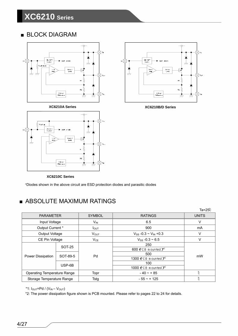
■BLOCK DIAGRAM
■ABSOLUTE MAXIMUM RATINGS Ta=25℃
*1: IOUT=Pd / (VIN – VOUT)
XC6210B/Dシリーズ
XC6210Cシリーズ
XC6210Aシリーズ
※ 上図のダイオードは静電保護用と寄生のダイオードになります。
XC6210A Series XC6210B/D Series
XC6210C Series
*Diodes shown in the above circuit are ESD protection diodes and parasitic diodes
*2: The power dissipation figure shown is PCB mounted. Please refer to pages 22 to 24 for details.

5/27
XC6210Series
PARAMETER SYMBOL CONDITIONS MIN. TYP. MAX. UNITS CIRCUIT
VIN=VOUT(T)+1.0V, IOUT=30mA VCE=ON (VIN or VSS) (VOUT(T)>1.50V) x 0.98 VOUT(T)
(*2) x 1.02 Output Voltage VOUT(E)
(*3) VIN=VOUT(T)+1.0V, IOUT=30mA, VCE=ON(VIN
or VSS)(VOUT(T)≦1.50V) (-30mV) VOUT(T)(*2) (+30mV)
V ①
VIN=VOUT(T)+1.0V,VCE=ON(VIN or VSS) (VOUT(T)>1.50V) 700 - -
Maximum Output Current IOUTMAX VIN=VOUT(T)+1.0V,VCE=ON(VIN or VSS)
(VOUT(T)≦1.50V) 500 - - mA ①
Load Regulation △VOUT 1mA<IOUT<100mA, VCE=ON(VIN or VSS) - 15 60 mV ①
Vdif1(*4) IOUT=30mA, VCE=ON(VIN or VSS) E-1 Dropout Voltage
Vdif2(*4) IOUT=100mA, VCE=ON(VIN or VSS) E-2 mV ①
Supply Current (A type) VIN=VCE=VOUT(T)+1.0V E-3
Supply Current (B type) VIN=VCE=VOUT(T)+1.0V - 35 55
Supply Current (C type) VIN=VOUT(T)+1.0V, VCE=VSS E-3
Supply Current (D type)
IDD
VIN=VOUT(T)+1.0V, VCE=VSS - 35 55
μA ②
Stand-by Current ISTBY VIN=6.0V,VCE=OFF(VIN or VSS) -0.10 - 0.10 μA ②
VOUT(T)+1.0V≦VIN≦6.0V VCE=ON(VIN or VSS), IOUT=30mA
VOUT(T)<4.50V Line Regulation △VOUT
△VIN・VOUT 5.5V≦VIN≦6.0V VCE=ON(VIN or VSS), IOUT=30mA
VOUT(T)≧4.50V
- 0.01 0.20 % / V ①
Input Voltage VIN - 1.5 - 6.0 V -
Output Voltage Temperature Characteristics
△VOUT △Topr・△VOUT
IOUT=30mA, VCE=ON (VIN or VSS) -40℃≦Topr≦85℃
- ±100 - ppm/℃ ①
VIN=[VOUT(T)+1.0]VDC+0.5VP-PAC VCE=ON(VIN or VSS), IOUT=30mA, f=1kHz
VOUT(T)<4.75V Ripple Rejection Rate PSRR
VIN=5.75VDC+0.5VP-PAC VCE=ON(VIN or VSS), IOUT=30mA, f=1kHz
VOUT(T)≧4.75V
- 60 - dB ③
VIN=VOUT(T)+1.0V, VCE=ON(VIN or VSS) VOUT(T)>1.50V 700 800 -
Current Limiter ILIM VIN=VOUT(T)+1.0V, VCE=ON(VIN or VSS)
VOUT(T)≦1.50V - 800 - mA ①
Short-Circuit Current ISHORT VIN=VOUT(T)+1.0V, VCE=ON(VIN or VSS) - 50 - mA ①
CE “High” Level Voltage VCEH - 1.3 - 6.0
CE “Low” Level Voltage VCEL - - - 0.25 V ①
CE “High” Level Current (A type) VCE=VIN=VOUT(T)+1.0V E-4 - E-4
CE “High” Level Current (B / C / D type)
ICEH VCE=VIN=VOUT(T)+1.0V - 0.10 - 0.10
μA ①
CE “Low” Level Current (C type) VIN=VOUT(T)+1.0V, VCE=VSS E-5 - E-5
CE “Low” Level Current (A / B / D type)
ICEL VIN=VOUT(T)+1.0V, VCE=VSS - 0.10 - 0.10
μA ①
Ta=25℃ ■ELECTRICAL CHARACTERISTICS●XC6210 series
NOTE: *1: Unless otherwise stated, VIN=VOUT(T)+1.0V *2: VOUT(T)=Specified output voltage *3: VOUT(E)=Effective output voltage
(i.e. the output voltage when " VOUT(T)+1.0V" is provided while maintaining a certain IOUT value). *4: Vdif ={VIN1
(*6)-VOUT1(*5) }
*5: A voltage equal to 98% of the output voltage whenever a stabilized VOUT1=IOUT{VOUT(T)+1.0V} is input. *6: VIN1= the input voltage when VOUT1, which appears as input voltage is gradually decreased. *7: VCE conditions: XC6210A / B type: ON=VIN, OFF=VSS
XC6210C / D type: ON=VSS, OFF=VIN

6/27
XC6210 Series
E-1 E-2 E-3 E-4 E-5 SETTING OUTPUT VOLTAGE
OUTPUT VOLTAGE
DROPOUT VOLTAGE 1 (IOUT=30mA)
DROPOUT VOLTAGE 2
(IOUT=100mA)
SUPPLY CURRENT
CE “H” LEVEL CURRENT
CE “L” LEVEL CURRENT
(V) (V) (mV) (mV) (μA) (μA) (μA)
VOUT Vdif1 Vdif2 IDD ICEH ICEL VOUT(T)
MIN. MAX. TYP. MAX. TYP. MAX. TYP. MAX. MIN. MAX. MIN. MAX.
0.80 0.770 0.830 0.85 0.820 0.880
700.0 800.0
0.90 0.870 0.930 0.95 0.920 0.980
100.0 600.0
250.0700.0
38.0 60.0 1.50 5.00 -5.00 -1.50
1.00 0.970 1.030 1.05 1.020 1.080
500.0 600.0
1.10 1.070 1.130 1.15 1.120 1.180
50.0 400.0
150.0500.0
1.20 1.170 1.230 1.25 1.220 1.280
300.0 400.0
1.30 1.270 1.330 1.35 1.320 1.380
200.0 300.0
1.40 1.370 1.430 1.45 1.420 1.480
30.0
100.0
100.0
250.0
38.5 61.5 2.00 6.50 -6.50 -2.00
1.50 1.470 1.530 1.55 1.519 1.581 1.60 1.568 1.632 1.65 1.617 1.683 1.70 1.666 1.734 1.75 1.715 1.785 1.80 1.764 1.836 1.85 1.813 1.887 1.90 1.862 1.938 1.95 1.911 1.989
27.0 41.0 90.0 135.0 39.0 63.0 2.50 8.00 -8.00 -2.50
2.00 1.960 2.040 2.05 2.009 2.091 2.10 2.058 2.142 2.15 2.107 2.193 2.20 2.156 2.244 2.25 2.205 2.295 2.30 2.254 2.346 2.35 2.303 2.397 2.40 2.352 2.448 2.45 2.401 2.499
25.0 37.0 80.0 120.0 39.5 64.5 3.00 9.50 -9.50 -3.00
2.50 2.450 2.550 2.55 2.499 2.601 2.60 2.548 2.652 2.65 2.597 2.703 2.70 2.646 2.754 2.75 2.695 2.805 2.80 2.744 2.856 2.85 2.793 2.907 2.90 2.842 2.958 2.95 2.891 3.009
18.0 28.0 60.0 90.0 40.0 66.0 3.50 11.00 -11.00 -3.50
●Dropout Voltage, Supply Current, CE “H / L” Level Current Chart
■VOLTAGE CHART
Ta=25℃

7/27
XC6210Series
E-1 E-2 E-3 E-4 E-5 SETTING OUTPUT VOLTAGE
OUTPUT VOLTAGE
DROPOUT VOLTAGE 1 (IOUT=30mA)
DROPOUT VOLTAGE 2
(IOUT=100mA)
SUPPLY CURRENT
CE “H” LEVEL CURRENT
CE “L” LEVEL CURRENT
(V) (V) (mV) (mV) (μA) (μA) (μA)
VOUT Vdif1 Vdif2 IDD ICEH ICEL VOUT(T)
MIN. MAX. TYP. MAX. TYP. MAX. TYP. MAX. MIN. MAX. MIN. MAX.
3.00 2.940 3.060 3.05 2.989 3.111 3.10 3.038 3.162 3.15 3.087 3.213 3.20 3.136 3.264 3.25 3.185 3.315 3.30 3.234 3.366 3.35 3.283 3.417 3.40 3.332 3.468 3.45 3.381 3.519
15.0 23.0 50.0 75.0 40.5 67.5 4.00 12.50 -12.50 -4.00
3.50 3.430 3.570 3.55 3.479 3.621 3.60 3.528 3.672 3.65 3.577 3.723 3.70 3.626 3.774 3.75 3.675 3.825 3.80 3.724 3.876 3.85 3.773 3.927 3.90 3.822 3.978 3.95 3.871 4.029
15 23 50 75 41.0 69.0 4.40 14.00 -14.00 -4.40
4.00 3.920 4.080 4.05 3.969 4.131 4.10 4.018 4.182 4.15 4.067 4.233 4.20 4.116 4.284 4.25 4.165 4.335 4.30 4.214 4.386 4.30 4.214 4.386 4.40 4.312 4.488 4.45 4.361 4.539
41.5 70.5 4.85 15.50 -15.50 -4.85
4.50 4.410 4.590 4.55 4.459 4.641 4.60 4.508 4.692 4.65 4.557 4.743 4.70 4.606 4.794 4.75 4.655 4.845 4.80 4.704 4.896 4.85 4.753 4.947 4.90 4.802 4.998 4.95 4.851 5.049 5.00 4.900 5.100
15.0 23.0 50.0 75.0
42.0 72.0 5.30 17.00 -17.00 -5.30
●Dropout Voltage, Supply Current, CE “H / L” Level Current Chart
■VOLTAGE CHART (Continued)
Ta=25℃

8/27
XC6210 Series
OUTPUT VOLTAGE CL
0.80V~1.45V More than 6.8μF
1.50V~1.75V More than 4.7μF
1.80V~5.00V More than 1.0μF
■TEST CIRCUITS ●Circuit① (Output Voltage, Maximum Output Voltage, Load Regulation, Dropout Voltage, Line Regulation, Output Voltage Temperature Characteristics, Current Limiter, Short-Circuit Current, CE “H” “L” Level Voltage, CE “H” “L” Level Current)
●Circuit ② (Supply Current, Stand-by Current)
●Circuit ③ (Ripple Rejection Rate)
●Output Capacitor Corresponding Chart
V A
VVIN
CIN
RLCLVCE
VIN
VOUT
CE
VSS V
A
IOUT
A
VIN
VOUTCE
VSS
VVIN

9/27
XC6210Series
VOUT CL 0.80V ~ 1.45V More than 6.8μF 1.50V ~ 1.75V More than 4.7μF 1.80V ~ 5.00V More than 1.0μF
■OPERATIONAL EXPLANATION<Output Voltage Regulator Control> The voltage, divided by resistors R1 & R2, which are connected to the VOUT pin is compared with the internal reference
voltage by the error amplifier. The P-channel MOSFET, which is connected to the VOUT pin, is then driven by the subsequent output signal. The output voltage at the VOUT pin is controlled & stabilized by negative feedback. The constant current limit circuit and short circuit protection operate in relation to the level of output current.
Output Capacitor Corresponding Chart
<Current Limiter, Short-Circuit Protection> The XC6210 series regulator offers a combination of current limit and short circuit protection by means of a built-in fixed current limiter circuit and a foldback circuit. When the load current reaches the current limit level, the fixed current limiter circuit operates and output voltage drops. As a result of this drop in output voltage, the foldback circuit operates, the output voltage drops further and output current decreases. When the output pin is shorted, a current of about 50mA flows.
<CE Pin>
The IC's internal regulator circuitry can be shut down via the signal from the CE pin with the XC6210 series. In shutdown mode, output at the VOUT pin will be pulled down to the VSS level via R1 & R2. Options are available for the CE pin logic (See the product classification). Note that as the XC6210B types are 'High Active / No Pull-Down', operations will become unstable with the CE pin open. Although the CE pin is equal to an inverter input with CMOS hysteresis, with either the pull-up or pull-down options, the CE pin input current will increase when the IC is in operation. We suggest that you use this IC with either a VIN voltage or a VSS voltage input at the CE pin. If this IC is used with the correct specifications for the CE pin, the IC will operate normally. However, supply current may increase as a result of through current in the IC's internal circuitry if a voltage other than VIN or VSS is applied.
<Low ESR Capacitor> With the XC6210 series regulator, a stable output voltage is achievable even if low ESR capacitors are used, as a phase compensation circuit is built into the regulator. In order to ensure the effectiveness of the phase compensation, we suggest that an output capacitor (CL) be connected as close as possible, between the output pin (VOUT) and the VSS pin. Please use an output capacitor (CL) with a capacitance, based on the chart below. We also suggest an input capacitor (CIN) of 1.0μF: this should be connected between VIN and VSS in order to stabilize input power source.
ON/OFFControl
each circuit
ErrorAmp
-
+
CurrentLimit
VIN
VSS
VOUT
R1
R2
VoltageReference
CE
10/27
XC6210 Series
■NOTES ON USE
1. Please use this IC within the stated absolute maximum ratings. For temporary, transitional voltage drop or voltage rising phenomenon, the IC is liable to malfunction should the ratings be exceeded.
2. Where wiring impedance is high, operations may become unstable due to noise and/or phase lag depending on output current. Please strengthen VIN and VSS wiring in particular.
3. Please wire the input capacitor (CIN) and the output capacitor (CL) as close to the IC as possible. If rapid input fluctuation or load fluctuation should occur, please increase the capacitor value such as CIN or CL more than the recommended values to stabilize the operation.
4. Torex places an importance on improving our products and its reliability. However, by any possibility, we would request user fail-safe design and post-aging treatment on system or equipment.

11/27
XC6210Series
■TYPICAL PERFORMANCE CHARACTERISTICS(1) Output Voltage vs. Output Current
XC6210x502xx
0.0
1.0
2.0
3.0
4.0
5.0
6.0
0 100 200 300 400 500 600 700 800 900
Output Current : IOUT(mA)
Out
put V
olta
ge :
VO
UT(V
)
VIN=6VVIN=5.8V
VIN=5.6VVIN=5.4V
Ta=25℃CIN=1.0μF(ceramic),CL=1.0μF(ceramic)
XC6210x502xx
0.0
1.0
2.0
3.0
4.0
5.0
6.0
0 100 200 300 400 500 600 700 800 900
Output Current : IOUT(mA)
Out
put
Vol
tage
: V
OUT
(V)
Ta=-40℃
Ta=25℃
Ta=85℃
VIN=6.0VCIN=1.0μF(ceramic),CL=1.0μF(ceramic)
XC6210x302xx
0.0
0.5
1.0
1.5
2.0
2.5
3.0
3.5
4.0
0 100 200 300 400 500 600 700 800 900
Output Current : IOUT(mA)
Out
put V
olta
ge :
VO
UT(
V)
VIN=3.2VVIN=3.5VVIN=4VVIN=5VVIN=6V
Ta=25℃CIN=1.0μF(ceramic),CL=1.0μF(ceramic)
XC6210x302xx
0.0
0.5
1.0
1.5
2.0
2.5
3.0
3.5
4.0
0 100 200 300 400 500 600 700 800 900
Output Current : IOUT(mA)
Out
put
Vol
tage
: V
OUT
(V)
Ta=-40℃
Ta=25℃
Ta=85℃
VIN=4.0VCIN=1.0μF(ceramic),CL=1.0μF(ceramic)
XC6210x082xx
0
0.1
0.2
0.3
0.4
0.5
0.6
0.7
0.8
0.9
0 100 200 300 400 500 600 700 800 900
Output Current : IOUT(mA)
Out
put V
olta
ge :
VO
UT(V
)
VIN=1.5VVIN=1.8V
VIN=3VVIN=6V
Ta=25℃CIN=1.0μF(ceramic),CL=6.8μF(ceramic)
XC6210x082xx
0
0.1
0.2
0.3
0.4
0.5
0.6
0.7
0.8
0.9
0 100 200 300 400 500 600 700 800 900
Output Current : IOUT(mA)
Out
put V
olta
ge :
VO
UT(V
)
Ta=-40℃
Ta=25℃
Ta=85℃
VIN=1.8VCIN=1.0μF(ceramic),CL=6.8μF(ceramic)

12/27
XC6210 Series
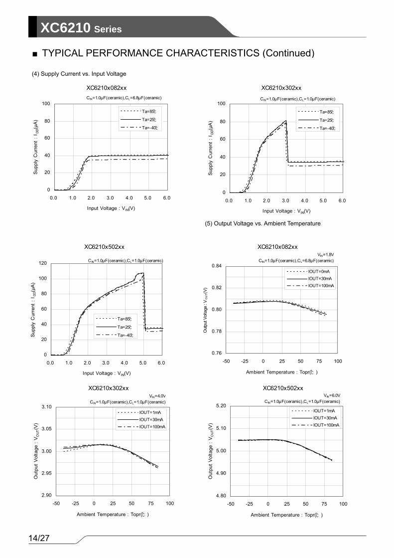
■TYPICAL PERFORMANCE CHARACTERISTICS (Continued)
(2) Output Voltage vs. Input Voltage
XC6210x502xx
4.2
4.4
4.6
4.8
5.0
5.2
4.5 5.0 5.5
Input Voltage : VIN(V)
Out
put V
olta
ge :
VO
UT(
V)
IOUT=0mAIOUT=30mAIOUT=100mA
Ta=25℃CIN=1.0μF(ceramic),CL=1.0μF(ceramic)
XC6210x502xx
4.85
4.90
4.95
5.00
5.05
5.10
5.5 5.6 5.7 5.8 5.9 6.0
Input Voltage : VIN(V)
Out
put V
olta
ge :
VO
UT(
V)
IOUT=0mAIOUT=30mAIOUT=100mA
Ta=25℃CIN=1.0μF(ceramic),CL=1.0μF(ceramic)
XC6210x302xx
2.2
2.4
2.6
2.8
3.0
3.2
2.5 3.0 3.5
Input Voltage : VIN(V)
Out
put
Vol
tage
: V
OUT
(V)
IOUT=0mAIOUT=30mAIOUT=100mA
Ta=25℃CIN=1.0μF(ceramic),CL=1.0μF(ceramic)
XC6210x302xx
2.85
2.90
2.95
3.00
3.05
3.10
3.5 4.0 4.5 5.0 5.5 6.0
Input Voltage : VIN(V)
Out
put V
olta
ge :
VO
UT(
V)
IOUT=0mAIOUT=30mAIOUT=100mA
Ta=25℃CIN=1.0μF(ceramic),CL=1.0μF(ceramic)
XC6210x082xx
0.5
0.6
0.7
0.8
0.9
1.0
1.1
0.5 1.0 1.5 2.0 2.5
Input Voltage : VIN(V)
Out
put
Volta
ge :
VO
UT(V
)
IOUT=0mAIOUT=30mAIOUT=100mA
Ta=25℃CIN=1.0μF(ceramic),CL=6.8μF(ceramic)
XC6210x082xx
0.65
0.70
0.75
0.80
0.85
0.90
1.5 2.0 2.5 3.0 3.5 4.0 4.5 5.0 5.5 6.0
Input Voltage : VIN(V)
Out
put
Volta
ge :
VO
UT(V
)
IOUT=0mAIOUT=30mAIOUT=100mA
Ta=25℃CIN=1.0μF(ceramic),CL=6.8μF(ceramic)

13/27
XC6210Series
■TYPICAL PERFORMANCE CHARACTERISTICS (Continued)
(3) Dropout Voltage vs. Output Current
XC6210x302xx
0.0
0.1
0.2
0.3
0.4
0.5
0.6
0 100 200 300 400 500 600 700
VR Output Current : IOUT(mA)
Dro
pout
Vol
tage
: Vd
if(V)
Ta=85℃
Ta=25℃
Ta=-40℃
CIN=1.0μF(ceramic),CL=1.0μF(ceramic)
XC6210x502xx
0.0
0.1
0.2
0.3
0.4
0.5
0.6
0 100 200 300 400 500 600 700
VR Output Current : IOUT(mA)
Dro
pout
Vol
tage
: Vd
if(V
)
Ta=85℃
Ta=25℃
Ta=-40℃
CIN=1.0μF(ceramic),CL=1.0μF(ceramic)
XC6210x082xx
0.0
0.10.2
0.30.4
0.5
0.60.7
0.80.9
1.0
0 100 200 300 400 500
Output Current : IOUT(mA)
Dro
pout
Vol
tage
: Vd
if(V
)
Ta=85℃
Ta=25℃
Ta=-40℃
CIN=1.0μF(ceramic),CL=6.8μF(ceramic)
Below the minimum operating voltage
XC6210x122xx
0.0
0.1
0.2
0.3
0.4
0.5
0.6
0.7
0.8
0 100 200 300 400 500
Output Current : IOUT(mA)
Dro
pout
Vol
tage
: Vd
if(V
)
Ta=85℃
Ta=25℃
Ta=-40℃
CIN=1.0μF(ceramic),CL=6.8μF(ceramic)
Below the minimum operating voltage
XC6210x252xx
0.0
0.1
0.2
0.3
0.4
0.5
0.6
0 100 200 300 400 500
VR Output Current : IOUT(mA)
Dro
pout
Vol
tage
: Vd
if(V
)
Ta=85℃
Ta=25℃
Ta=-40℃
CIN=1.0μF(ceramic),CL=1.0μF(ceramic)
XC6210x152xx
0.0
0.1
0.2
0.3
0.4
0.5
0.6
0 100 200 300 400 500
VR Output Current : IOUT(mA)
Dro
pout
Vol
tage
: V
dif(
V)
Ta=85℃
Ta=25℃
Ta=-40℃
CIN=1.0μF(ceramic),CL=2.2μF(ceramic)
14/27
XC6210 Series
■TYPICAL PERFORMANCE CHARACTERISTICS (Continued)
(4) Supply Current vs. Input Voltage
XC6210x502xx
4.80
4.90
5.00
5.10
5.20
-50 -25 0 25 50 75 100
Ambient Temperature : Topr(℃)
Out
put
Volta
ge :
VO
UT(
V)
IOUT=1mAIOUT=30mAIOUT=100mA
VIN=6.0VCIN=1.0μF(ceramic),CL=1.0μF(ceramic)
XC6210x302xx
2.90
2.95
3.00
3.05
3.10
-50 -25 0 25 50 75 100
Ambient Temperature : Topr(℃)
Out
put
Volta
ge :
VO
UT(
V)
IOUT=1mAIOUT=30mAIOUT=100mA
VIN=4.0VCIN=1.0μF(ceramic),CL=1.0μF(ceramic)
XC6210x082xx
0
20
40
60
80
100
0.0 1.0 2.0 3.0 4.0 5.0 6.0
Input Voltage : VIN(V)
Supp
ly C
urre
nt :
I DD(μ
A)
Ta=85℃
Ta=25℃
Ta=-40℃
CIN=1.0μF(ceramic),CL=6.8μF(ceramic)
XC6210x302xx
0
20
40
60
80
100
0.0 1.0 2.0 3.0 4.0 5.0 6.0
Input Voltage : VIN(V)Su
pply
Cur
rent
: I
DD(μ
A)
Ta=85℃
Ta=25℃
Ta=-40℃
CIN=1.0μF(ceramic),CL=1.0μF(ceramic)
XC6210x082xx
0.76
0.78
0.80
0.82
0.84
-50 -25 0 25 50 75 100
Ambient Temperature : Topr(℃)
Out
put V
olta
ge :
VO
UT(
V)
IOUT=0mAIOUT=30mAIOUT=100mA
VIN=1.8VCIN=1.0μF(ceramic),CL=6.8μF(ceramic)
XC6210x502xx
0
20
40
60
80
100
120
0.0 1.0 2.0 3.0 4.0 5.0 6.0
Input Voltage : VIN(V)
Supp
ly C
urre
nt :
ID
D(μA
)
Ta=85℃
Ta=25℃
Ta=-40℃
CIN=1.0μF(ceramic),CL=1.0μF(ceramic)
(5) Output Voltage vs. Ambient Temperature

15/27
XC6210Series
■TYPICAL PERFORMANCE CHARACTERISTICS (Continued)
(6) Supply Current vs. Ambient Temperature
(7) CE Pin Threshold Voltage vs. Ambient Temperature
XC6210x502xx
25
30
35
40
45
50
-50 -25 0 25 50 75 100
Ambient Temperature : Topr(℃)
Sup
ply
Cur
rent
: I D
D(μ
A)
VIN=6.0VCIN=1.0μF(ceramic),CL=1.0μF(ceramic)
XC6210x082xx
25
30
35
40
45
50
-50 -25 0 25 50 75 100
Ambient Temperature : Topr(℃)
Supp
ly C
urre
nt :
I DD(μ
A)
VIN=1.8VCIN=1.0μF(ceramic),CL=6.8μF(ceramic)
XC6210x302xx
25
30
35
40
45
50
-50 -25 0 25 50 75 100
Ambient Temperature : Topr(℃)S
uppl
y C
urre
nt :
I DD(μ
A)
VIN=4.0VCIN=1.0μF(ceramic),CL=1.0μF(ceramic)
XC6210xxxxxx
0.7
0.8
0.9
1.0
1.1
-50 -25 0 25 50 75 100
Ambient Temperature : Topr(℃)
CE
Thr
esho
ld V
olta
ge :
VC
EH/V
CE
L(V)
H Level Voltage
L Level Voltage
VIN=VOUT+1.0VCIN=1.0μF(ceramic),CL=1.0μF(ceramic)

16/27
XC6210 Series
■TYPICAL PERFORMANCE CHARACTERISTICS (Continued)
(8) Input Transient Response 1
XC6210x082xx
0.6
0.7
0.8
0.9
1.0
1.1
1.2
Time (20μs/div )O
utpu
t Vo
ltage
: V
OU
T(V
)
-2.0
-1.0
0.0
1.0
2.0
3.0
4.0
Inpu
t Vo
ltage
: V
IN(V
)
IOUT=200mA,tr=tf=5.0μsCL=6.8μF(ceramic),Ta=25℃
Input Voltage
Output Voltage
XC6210x082xx
0.6
0.7
0.8
0.9
1.0
1.1
1.2
Time (20μs/div )
Out
put V
olta
ge :
VO
UT(V
)
-2.0
-1.0
0.0
1.0
2.0
3.0
4.0
Inpu
t Vol
tage
: V
IN(V
)
IOUT=30mA,tr=tf=5.0μsCL=6.8μF(ceramic),Ta=25℃
Input Voltage
Output Voltage
XC6210x302xx
2.8
2.9
3.0
3.1
3.2
3.3
3.4
Time (20μs/div )
Out
put
Volta
ge :
VO
UT(V
)
0.0
1.0
2.0
3.0
4.0
5.0
6.0
Inpu
t Vo
ltage
: V
IN(V
)
IOUT=200mA,tr=tf=5.0μsCL=1.0μF(ceramic),Ta=25℃
Input Voltage
Output Voltage
XC6210x302xx
2.8
2.9
3.0
3.1
3.2
3.3
3.4
Time (20μs/div )
Out
put V
olta
ge :
VO
UT(V
)
0.0
1.0
2.0
3.0
4.0
5.0
6.0
Inpu
t Vol
tage
: V
IN(V
)
IOUT=30mA,tr=tf=5.0μsCL=1.0μF(ceramic),Ta=25℃
Input Voltage
Output Voltage
XC6210x502xx
4.8
4.9
5.0
5.1
5.2
5.3
5.4
Time (20μs/div )
Out
put V
olta
ge :
VO
UT(V
)
2.0
3.0
4.0
5.0
6.0
7.0
8.0
Inpu
t Vol
tage
: V
IN(V
)
IOUT=200mA,tr=tf=5.0μsCL=1.0uF(ceramic),Ta=25℃
Input Voltage
Output Voltage
XC6210x502xx
4.8
4.9
5.0
5.1
5.2
5.3
5.4
Time (20μs/div )
Out
put
Volta
ge :
VO
UT(V
)
2.0
3.0
4.0
5.0
6.0
7.0
8.0
Inpu
t Vo
ltage
: V
IN(V
)
IOUT=30mA,tr=tf=5.0μsCL=1.0uF(ceramic),Ta=25℃
Input Voltage
Output Voltage

17/27
XC6210Series
■TYPICAL PERFORMANCE CHARACTERISTICS (Continued)
(9) Load Transient Response
XC6210x082xx
0.0
0.2
0.4
0.6
0.8
1.0
Time (25μs/div )
Out
put V
olta
ge :
VO
UT(V
)
0
100
200
300
400
500
Out
put C
urre
nt :
I OU
T(m
A)
VIN=1.8V,tr=tf=5.0μs,Ta=25℃CIN=1.0μF(ceramic),CL=6.8μF(ceramic)
Output Current
Output Voltage
10mA
100mA
XC6210x082xx
0.0
0.2
0.4
0.6
0.8
1.0
Time (25μs/div )
Out
put
Volta
ge :
VO
UT(V
)0
100
200
300
400
500
Out
put
Cur
rent
: I O
UT(
mA)
VIN=1.8V,tr=tf=5.0μs,Ta=25℃CIN=1.0μF(ceramic),CL=6.8μF(ceramic)
Output Current
Output Voltage
10mA
200mA
XC6210x302xx
1.4
1.8
2.2
2.6
3.0
3.4
Time (25μs/div )
Out
put V
olta
ge :
V OUT
(V)
0
100
200
300
400
500
Out
put C
urre
nt :
I OU
T(m
A)
VIN=4.0V,tr=tf=5.0μs,Ta=25℃CIN=1.0μF(ceramic),CL=1.0μF(ceramic)
Output Current
Output Voltage
10mA
100mA
XC6210x302xx
1.4
1.8
2.2
2.6
3.0
3.4
Time (25μs/div )
Out
put V
olta
ge :
V OUT
(V)
0
100
200
300
400
500
Out
put C
urre
nt :
I OU
T(m
A)
VIN=4.0V,tr=tf=5.0μs,Ta=25℃CIN=1.0μF(ceramic),CL=1.0μF(ceramic)
Output Current
Output Voltage
10mA
200mA
XC6210x502xx
3.4
3.8
4.2
4.6
5.0
5.4
Time (25μs/div )
Out
put V
olta
ge :
VO
UT(V
)
0
100
200
300
400
500
Out
put
Cur
rent
: I O
UT(m
A)
VIN=6.0V,tr=tf=5.0μs,Ta=25℃CIN=1.0μF(ceramic),CL=1.0μF(ceramic)
Output Current
Output Voltage
10mA
100mA
XC6210x502xx
3.4
3.8
4.2
4.6
5.0
5.4
Time (25μs/div )
Out
put
Volta
ge :
VO
UT(V
)
0
100
200
300
400
500
Out
put
Cur
rent
: I O
UT(
mA)
VIN=6.0V,tr=tf=5.0μs,Ta=25℃CIN=1.0μF(ceramic),CL=1.0μF(ceramic)
Output Current
Output Voltage
10mA
200mA

18/27
XC6210 Series
■TYPICAL PERFORMANCE CHARACTERISTICS (Continued)
(10) Ripple Rejection Rate
XC6210x302xx
0
10
20
30
40
50
60
70
80
0.01 0.1 1 10 100
Ripple Frequency : f (kHz)R
ippl
e R
ejec
tion
Rat
e : P
SR
R(d
B)
VIN=4.0VDC+0.5VP-PAC,IOUT=30mA,Ta=25℃CIN=1.0μF(ceramic),CL=1.0μF(ceramic)
XC6210x082xx
0
10
20
30
40
50
60
70
80
0.01 0.1 1 10 100
Ripple Frequency : f (kHz)
Rip
ple
Rej
ectio
n R
ate
: PS
RR
(dB
)
VIN=1.8VDC+0.5VP-PAC,IOUT=30mA,Ta=25℃CIN=1.0μF(ceramic),CL=6.8μF(ceramic)
XC6210x502xx
0
10
20
30
40
50
60
70
80
0.01 0.1 1 10 100
Ripple Frequency : f (kHz)
Rip
ple
Rej
ectio
n R
ate
: PS
RR
(dB)
VIN=5.75VDC+0.5VP-PAC,IOUT=30mA,Ta=25℃CIN=1.0μF(ceramic),CL=1.0μF(ceramic)

19/27
XC6210Series
■TYPICAL PERFORMANCE CHARACTERISTICS (Continued) (11) Input Transient Response 2
XC6210x082xx
0.0
1.0
2.0
3.0
4.0
5.0
Time (25μs/div )O
utpu
t Vol
tage
: V O
UT(V
)
-6.0
-4.0
-2.0
0.0
2.0
4.0
CE
Inpu
t Vol
tage
: V C
E(V
)
Output Voltage
CE Input Voltage
VIN=1.8V,IOUT=30mA,tr=5.0μsCIN=1.0μF(ceramic),CL=6.8μF(ceramic),Ta=25℃
XC6210x082xx
0.0
1.0
2.0
3.0
4.0
5.0
Time (25μs/div )
Out
put
Volta
ge :
VO
UT(V
)
-6.0
-4.0
-2.0
0.0
2.0
4.0
CE
Inpu
t Vo
ltage
: V
CE(
V)
VIN=1.8V,IOUT=30mA,tr=5.0μsCIN=1.0μF(ceramic),CL=6.8μF(ceramic),Ta=25℃
Output Voltage
CE Input Voltage
XC6210x302xx
0.0
1.0
2.0
3.0
4.0
5.0
Time (25μs/div )
Out
put V
olta
ge :
VO
UT(
V)
-4.0
-2.0
0.0
2.0
4.0
6.0
CE
Inpu
t Vol
tage
: V
CE(V
)
VIN=4.0V,IOUT=30mA,tr=5.0μsCIN=1.0μF(ceramic),CL=1.0μF(ceramic),Ta=25℃
Output Voltage
CE Input Voltage
XC6210x302xx
0.0
1.0
2.0
3.0
4.0
5.0
Time (25μs/div )
Out
put
Volta
ge :
VO
UT(V
)
-4.0
-2.0
0.0
2.0
4.0
6.0
CE
Inpu
t Vo
ltage
: V
CE(
V)
VIN=4.0V,IOUT=30mA,tr=5.0μsCIN=1.0μF(ceramic),CL=1.0μF(ceramic),Ta=25℃
Output Voltage
CE Input Voltage
XC6210x502xx
0.0
2.0
4.0
6.0
8.0
10.0
Time (25μs/div )
Out
put V
olta
ge :
VO
UT(V
)
-2.0
0.0
2.0
4.0
6.0
8.0
CE
Inpu
t Vol
tage
: V
CE(V
)
VIN=6.0V,IOUT=30mA,tr=5.0μsCIN=1.0μF(ceramic),CL=1.0μF(ceramic),Ta=25℃
Output Voltage
CE Input Voltage
XC6210x502xx
0.0
2.0
4.0
6.0
8.0
10.0
Time (25μs/div )
Out
put V
olta
ge :
VO
UT(V
)
-2.0
0.0
2.0
4.0
6.0
8.0
CE
Inpu
t Vo
ltage
: V
CE(V
)
VIN=6.0V,IOUT=30mA,tr=5.0μsCIN=1.0μF(ceramic),CL=1.0μF(ceramic),Ta=25℃
Output Voltage
CE Input Voltage
20/27
XC6210 Series
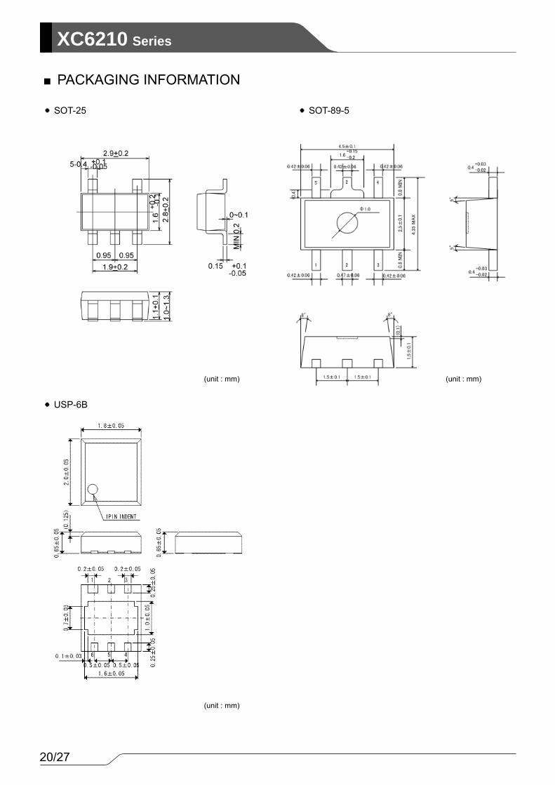
●SOT-25 ●SOT-89-5
●USP-6B
■PACKAGING INFORMATION
(unit : mm) (unit : mm)
(unit : mm)

21/27
XC6210Series
■PACKAGING INFORMATION (Continued)
●USP-6B Reference Pattern Layout ●USP-6B Reference Metal Mask Design
(unit : mm) (unit : mm)

22/27
XC6210 Series
●SOT-25 Power Dissipation
評価基板レイアウト(単位:mm)
Board Mount (Tj max = 125℃)
Ambient Temperature(℃) Power Dissipation Pd(mW) Thermal Resistance (℃/W)
25 600
85 240 166.67
Power dissipation data for the SOT-25 is shown in this page. The value of power dissipation varies with the mount board conditions. Please use this data as one of reference data taken in the described condition.
1. Measurement Condition (Reference data) Condition: Mount on a board Ambient: Natural convection Soldering: Lead (Pb) free Board: Dimensions 40 x 40 mm (1600 mm2 in one side)
Copper (Cu) traces occupy 50% of the board area In top and back faces Package heat-sink is tied to the copper traces (Board of SOT-26 is used.)
Material: Glass Epoxy (FR-4) Thickness: 1.6 mm Through-hole: 4 x 0.8 Diameter
Evaluation Board (Unit: mm)
2. Power Dissipation vs. Ambient temperature
■PACKAGING INFORMATION (Continued)
Pd-Ta特性グラフ
0
100
200
300
400
500
600
700
25 45 65 85 105 125
周辺温度Ta(℃)
許容損失Pd(mW)
Ambient Temperature Ta (℃)
Pow
er D
issi
patio
n Pd
(mW
)
Pd vs. Ta

23/27
XC6210Series
● SOT-89-5 Power Dissipation
て
Board Mount (Tj max = 125℃)
Ambient Temperature(℃) Power Dissipation Pd(mW) Thermal Resistance (℃/W)
25 1300
85 520 76.92
Power dissipation data for the SOT-89-5 is shown in this page. The value of power dissipation varies with the mount board conditions. Please use this data as one of reference data taken in the described condition.
1. Measurement Condition (Reference data) Condition: Mount on a board Ambient: Natural convection Soldering: Lead (Pb) free Board: Dimensions 40 x 40 mm (1600 mm2 in one side)
Copper (Cu) traces occupy 50% of the board area In top and back faces Package heat-sink is tied to the copper traces
Material: Glass Epoxy (FR-4) Thickness: 1.6 mm Through-hole: 5 x 0.8 Diameter
Evaluation Board (Unit: mm) 2. Power Dissipation vs. Ambient temperature
■PACKAGING INFORMATION (Continued)
Pd-Ta特性グラフ
0
200
400
600
800
1000
1200
1400
25 45 65 85 105 125
周辺温度Ta(℃)
許容損失Pd(mW)
Pd vs. Ta
Ambient Temperature Ta (℃)
Pow
er D
issi
patio
n P
d (m
W)

24/27
XC6210 Series
● USP-6B Power Dissipation
て
Board Mount (Tj max = 125℃)
Ambient Temperature(℃) Power Dissipation Pd(mW) Thermal Resistance (℃/W)
25 1000
85 400 100.00
Pd-Ta特性グラフ
0
200
400
600
800
1000
1200
25 45 65 85 105 125
周辺温度Ta(℃)
許容損失Pd(mW)
■PACKAGING INFORMATION (Continued)
Power dissipation data for the USP-6B is shown in this page. The value of power dissipation varies with the mount board conditions. Please use this data as one of reference data taken in the described condition.
1. Measurement Condition (Reference data) Condition: Mount on a board Ambient: Natural convection Soldering: Lead (Pb) free Board: Dimensions 40 x 40 mm (1600 mm2 in one side)
Copper (Cu) traces occupy 50% of the board area In top and back faces Package heat-sink is tied to the copper traces
Material: Glass Epoxy (FR-4) Thickness: 1.6 mm Through-hole: 4 x 0.8 Diameter
Evaluation Board (Unit: mm) 2. Power Dissipation vs. Ambient temperature
Pd vs. Ta
Ambient Temperature Ta (℃)
Pow
er D
issi
patio
n P
d (m
W)
25/27
XC6210Series
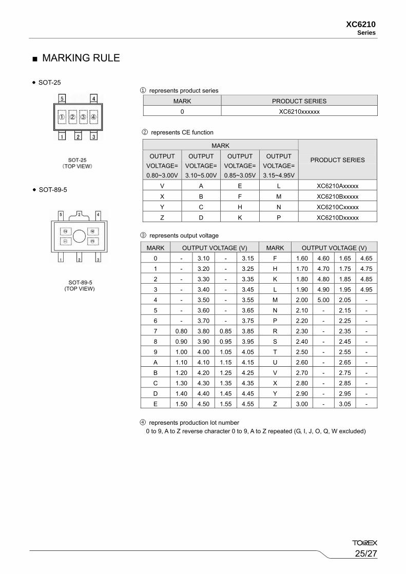
MARK PRODUCT SERIES
0 XC6210xxxxxx
MARK
OUTPUT VOLTAGE=0.80~3.00V
OUTPUT VOLTAGE=3.10~5.00V
OUTPUT VOLTAGE=0.85~3.05V
OUTPUT VOLTAGE= 3.15~4.95V
PRODUCT SERIES
V A E L XC6210Axxxxx
X B F M XC6210Bxxxxx
Y C H N XC6210Cxxxxx
Z D K P XC6210Dxxxxx
MARK OUTPUT VOLTAGE (V) MARK OUTPUT VOLTAGE (V)
0 - 3.10 - 3.15 F 1.60 4.60 1.65 4.65
1 - 3.20 - 3.25 H 1.70 4.70 1.75 4.75
2 - 3.30 - 3.35 K 1.80 4.80 1.85 4.85
3 - 3.40 - 3.45 L 1.90 4.90 1.95 4.95
4 - 3.50 - 3.55 M 2.00 5.00 2.05 -
5 - 3.60 - 3.65 N 2.10 - 2.15 -
6 - 3.70 - 3.75 P 2.20 - 2.25 -
7 0.80 3.80 0.85 3.85 R 2.30 - 2.35 -
8 0.90 3.90 0.95 3.95 S 2.40 - 2.45 -
9 1.00 4.00 1.05 4.05 T 2.50 - 2.55 -
A 1.10 4.10 1.15 4.15 U 2.60 - 2.65 -
B 1.20 4.20 1.25 4.25 V 2.70 - 2.75 -
C 1.30 4.30 1.35 4.35 X 2.80 - 2.85 -
D 1.40 4.40 1.45 4.45 Y 2.90 - 2.95 -
E 1.50 4.50 1.55 4.55 Z 3.00 - 3.05 -
■MARKING RULE
① represents product series
② represents CE function
③ represents output voltage
④ represents production lot number 0 to 9, A to Z reverse character 0 to 9, A to Z repeated (G, I, J, O, Q, W excluded)
●SOT-25
●SOT-89-5
SOT-89-5 (TOP VIEW)

26/27
XC6210 Series
MARK VOLTAGE
(V) PRODUCT
SERIES MARK
VOLTAGE (V)
PRODUCT SERIES
0 x.00 XC6210xx02Dx A x.05 XC6210xx0ADx1 x.10 XC6210xx12Dx B x.15 XC6210xx1ADx2 x.20 XC6210xx22Dx C x.25 XC6210xx2ADx3 x.30 XC6210xx32Dx D x.35 XC6210xx3ADx4 x.40 XC6210xx42Dx E x.45 XC6210xx4ADx5 x.50 XC6210xx52Dx F x.55 XC6210xx5ADx6 x.60 XC6210xx62Dx H x.65 XC6210xx6ADx7 x.70 XC6210xx72Dx K x.75 XC6210xx7ADx8 x.80 XC6210xx82Dx L x.85 XC6210xx8ADx9 x.90 XC6210xx92Dx M x.95 XC6210xx9ADx
MARK
① ② PRODUCT SERIES
1 0 XC6210xxxxxx
MARK TYPE PRODUCT SERIES
A CE High Active with pull-down resistor XC6210AxxxDx
B CE High Active with no pull-down resistor XC6210BxxxDx
C CE Low Active with pull-up resistor XC6210CxxxDx
D CE Low Active with no pull-up resistor XC6210DxxxDx
MARK VOLTAGE (V) PRODUCT SERIES
3 3.x XC6210x3xxDx
5 5.x XC6210x5xxDx
●USP-6B ①② represents product series
③ represents CE Function
④ represents the integer number of output voltage ex.)
⑥ represents production lot number 0 to 9, A to Z repeated (G, I, J, O, Q, W, excluded) Note: No character inversion used.
USP-6B (TOP VIEW)
⑤ represents the decimal point of output voltage
■MARKING RULE (Continued)

27/27
XC6210Series
1. The products and product specifications contained herein are subject to change without
notice to improve performance characteristics. Consult us, or our representatives
before use, to confirm that the information in this datasheet is up to date.
2. We assume no responsibility for any infringement of patents, patent rights, or other
rights arising from the use of any information and circuitry in this datasheet.
3. Please ensure suitable shipping controls (including fail-safe designs and aging
protection) are in force for equipment employing products listed in this datasheet.
4. The products in this datasheet are not developed, designed, or approved for use with
such equipment whose failure of malfunction can be reasonably expected to directly
endanger the life of, or cause significant injury to, the user.
(e.g. Atomic energy; aerospace; transport; combustion and associated safety
equipment thereof.)
5. Please use the products listed in this datasheet within the specified ranges.
Should you wish to use the products under conditions exceeding the specifications,
please consult us or our representatives.
6. We assume no responsibility for damage or loss due to abnormal use.
7. All rights reserved. No part of this datasheet may be copied or reproduced without the
prior permission of TOREX SEMICONDUCTOR LTD.