Embed Size (px)
Citation preview
1/17
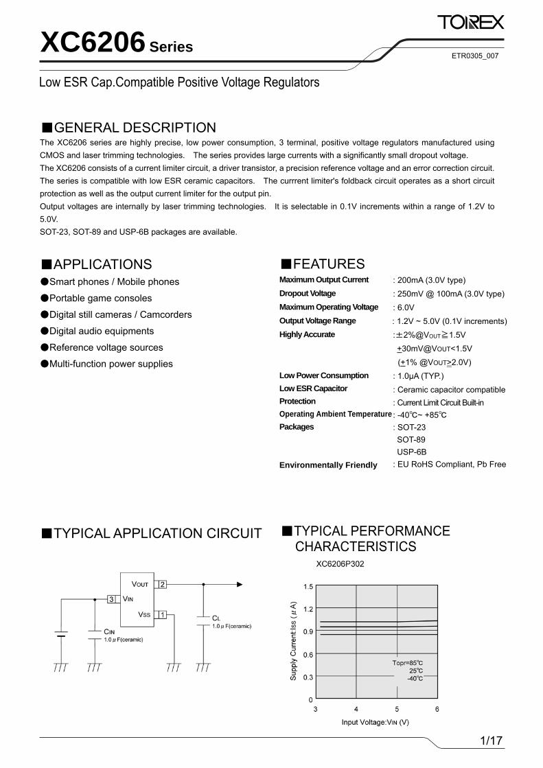
ETR0305_007 XC6206 Series
■APPLICATIONS ●Smart phones / Mobile phones
●Portable game consoles
●Digital still cameras / Camcorders
●Digital audio equipments
●Reference voltage sources
●Multi-function power supplies
■TYPICAL APPLICATION CIRCUIT
■FEATURESMaximum Output Current Dropout Voltage Maximum Operating Voltage Output Voltage Range Highly Accurate Low Power Consumption Low ESR Capacitor Protection Operating Ambient Temperature Packages Environmentally Friendly
■TYPICAL PERFORMANCE CHARACTERISTICS
: 200mA (3.0V type)
: 250mV @ 100mA (3.0V type)
: 6.0V
: 1.2V ~ 5.0V (0.1V increments)
:±2%@VOUT≧1.5V
+30mV@VOUT<1.5V
(+1% @VOUT>2.0V)
: 1.0μA (TYP.)
: Ceramic capacitor compatible : Current Limit Circuit Built-in : -40℃~ +85℃ : SOT-23 SOT-89 USP-6B : EU RoHS Compliant, Pb Free
■GENERAL DESCRIPTION The XC6206 series are highly precise, low power consumption, 3 terminal, positive voltage regulators manufactured using CMOS and laser trimming technologies. The series provides large currents with a significantly small dropout voltage. The XC6206 consists of a current limiter circuit, a driver transistor, a precision reference voltage and an error correction circuit.The series is compatible with low ESR ceramic capacitors. The currrent limiter's foldback circuit operates as a short circuit protection as well as the output current limiter for the output pin. Output voltages are internally by laser trimming technologies. It is selectable in 0.1V increments within a range of 1.2V to 5.0V. SOT-23, SOT-89 and USP-6B packages are available.
2/20
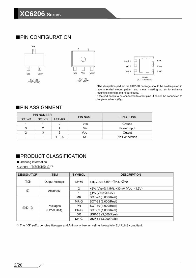
XC6206 Series
PIN NUMBER PIN NAME FUNCTIONS
SOT-23 SOT-89 USP-6B 1 1 2 VSS Ground 3 2 4 VIN Power Input 2 3 6 VOUT Output - - 1, 3, 5 NC No Connection
DESIGNATOR ITEM SYMBOL DESCRIPTION
①② Output Voltage 12~50 e.g. VOUT: 3.0V→①=3, ②=0
③ Accuracy 2 +2% (VOUT≧1.5V), +30mV (VOUT<1.5V) 1 +1% (VOUT≧2.0V)
④⑤-⑥ Packages
(Order Unit)
MR SOT-23 (3,000/Reel) MR-G SOT-23 (3,000/Reel)
PR SOT-89 (1,000/Reel) PR-G SOT-89 (1,000/Reel) DR USP-6B (3,000/Reel)
DR-G USP-6B (3,000/Reel)
●Ordering Information
XC6206P ①②③④⑤-⑥(*1)
■PIN CONFIGURATION
■PIN ASSIGNMENT
■PRODUCT CLASSIFICATION
*The dissipation pad for the USP-6B package should be solder-plated inrecommended mount pattern and metal masking so as to enhancemounting strength and heat release. If the pad needs to be connected to other pins, it should be connected tothe pin number 4 (VIN).
(*1) The “-G” suffix denotes Halogen and Antimony free as well as being fully EU RoHS compliant.
3/20
XC6206Series
Ta=25OC
PARAMETER SYMBOL RATINGS UNITSInput Voltage VIN -0.3~+7.0 V
Output Current IOUT 500 (*1) mA Output Voltage VOUT -0.3 ~ VIN + 0.3 V
Power Dissipation
SOT-23
Pd
250
mW
500(PCB mounted) (*2)
SOT-89 500
1000(PCB mounted) (*2)
USP-6B 120
1000(PCB mounted) (*2) Operating Ambient Temperature Topr - 40 ~ + 85 OC
Storage Temperature Tstg - 55 ~ + 125 OC
■ABSOLUTE MAXIMUM RATINGS
(*1) IOUT≦Pd / (VIN-VOUT) (*2) This power dissipation figure shown is PCB mounted and is for reference only. Please refer to page 15~17 for details.
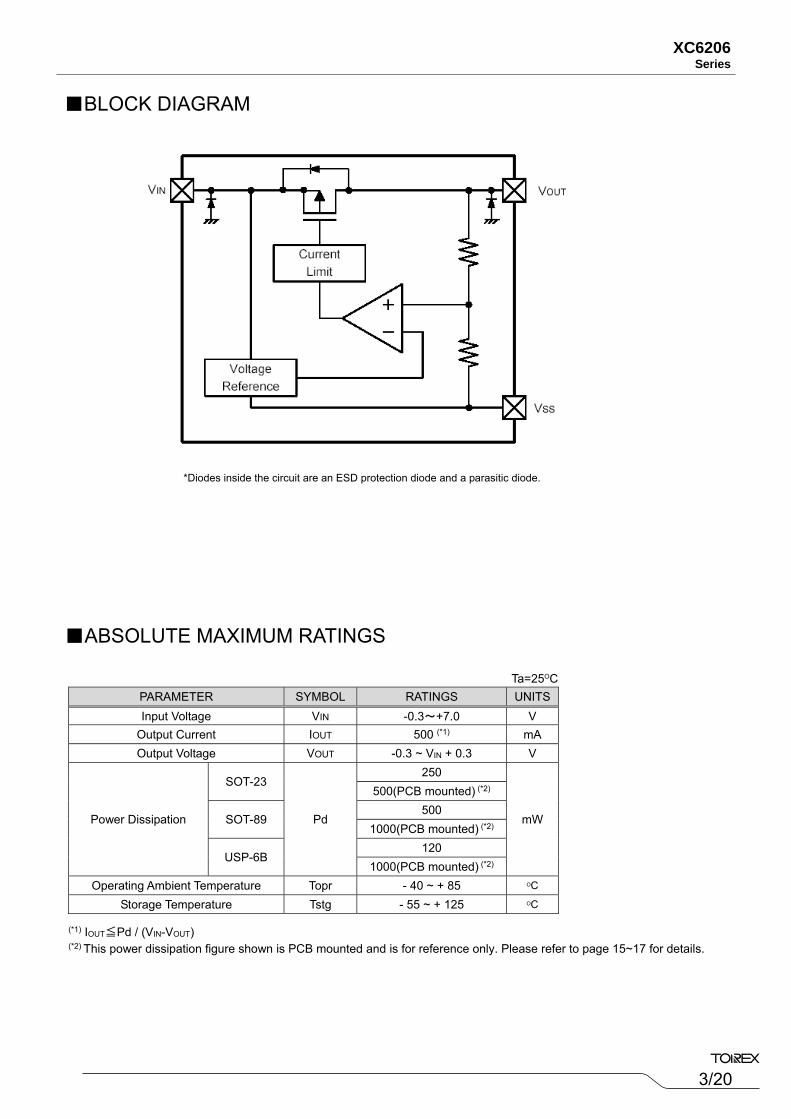
■BLOCK DIAGRAM
*Diodes inside the circuit are an ESD protection diode and a parasitic diode.
4/20
XC6206 Series
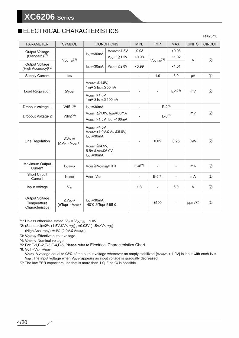
PARAMETER SYMBOL CONDITIONS MIN. TYP. MAX. UNITS CIRCUIT
Output Voltage (Standard)(*2)
VOUT(E)(*3)
IOUT=30mAVOUT(T)<1.5V -0.03
VOUT(T)(*4)
+0.03
V ② VOUT(T)≧1.5V ×0.98 ×1.02
Output Voltage (High Accuracy)(*2) IOUT=30mA VOUT(T)≧2.0V ×0.99 ×1.01
Supply Current IDD - 1.0 3.0 μA ①
Load Regulation ∆VOUT
VOUT(T)≦1.8V, 1mA≦IOUT≦50mA
- - E-1(*5) mV ② VOUT(T)>1.8V, 1mA≦IOUT≦100mA
Dropout Voltage 1 Vdif1(*6) IOUT=30mA - E-2(*5)
mV ② Dropout Voltage 2 Vdif2(*6)
VOUT(T)≦1.8V, IOUT=60mA- E-3(*5)
VOUT(T)>1.8V, IOUT=100mA
Line Regulation ∆VOUT/ (∆VIN・VOUT)
VOUT(T)<4.5V, VOUT(T)+1.0V≦VIN≦6.0V, IOUT=30mA
- 0.05 0.25 %/V ② VOUT(T)≧4.5V, 5.5V≦VIN≦6.0V, IOUT=30mA
Maximum Output Current IOUTMAX VOUT≧VOUT(E)× 0.9 E-4(*5) - - mA ②
Short Circuit Current ISHORT VOUT=VSS - E-5(*5) - mA ②
Input Voltage VIN 1.8 - 6.0 V ②
Output Voltage Temperature
Characteristics
∆VOUT/ (∆Topr・VOUT)
IOUT=30mA, -40℃≦Topr≦85℃ - ±100 - ppm/℃ ②
■ELECTRICAL CHARACTERISTICS
*1: Unless otherwise stated, VIN = VOUT(T) + 1.0V *2: (Standard):±2% (1.5V≦VOUT(T)) , ±0.03V (1.5V>VOUT(T)) (High Accuracy):±1% (2.0V≦VOUT(T)) *3: VOUT(E) :Effective output voltage. *4: VOUT(T) :Nominal voltage *5: For E-1,E-2,E-3,E-4,E-5, Please refer to Electrical Characteristics Chart. *6: Vdif =VIN1 -VOUT1
VOUT1 :A voltage equal to 98% of the output voltage whenever an amply stabilized {VOUT(T) + 1.0V} is input with each IOUT. VIN1 :The input voltage when VOUT1 appears as input voltage is gradually decreased.
*7: The low ESR capacitors use that is more than 1.0μF as CL is possible.
Ta=25 OC
5/20
XC6206Series
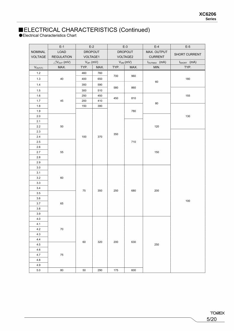
●Electrical Characteristics Chart
NOMINAL VOLTAGE
E-1 E-2 E-3 E-4 E-5
LOAD REGULATION
DROPOUT VOLTAGE1
DROPOUT VOLTAGE2
MAX. OUTPUT CURRENT
SHORT CURRENT
⊿VOUT (mV) Vdif1 (mV) Vdif2 (mV) IOUTMAX (mA) ISHORT (mA) VOUT(T) MAX. TYP. MAX. TYP. MAX. MIN. TYP.
1.2
40
460 760 700 960
60 180 1.3 400 650
1.4 350 590 580 860
1.5
45
300 510
155 1.6 250 450 450 810
80 1.7 200 410
1.8 150 390
350
780
130
1.9
100 370
2.0
50 120
2.1
710
2.2
2.3
100
2.4
2.5
55 150
2.6
2.7
2.8
2.9
3.0
60
75 350 250 680 200
3.1
3.2
3.3
3.4
3.5
65
3.6
3.7
3.8
3.9
4.0
70
60 320 200 630 250
4.1
4.2
4.3
4.4
4.5
75
4.6
4.7
4.8
4.9
5.0 80 50 290 175 600
■ELECTRICAL CHARACTERISTICS (Continued)
6/20
XC6206 Series
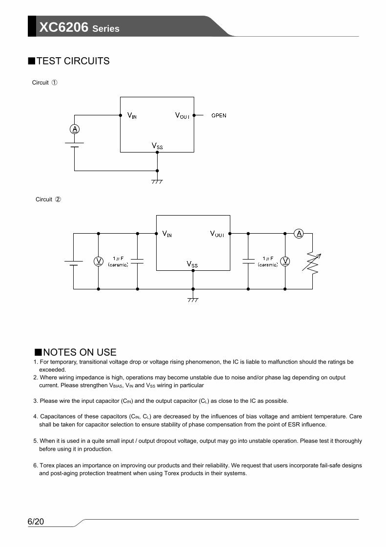
■TEST CIRCUITS
Circuit ①
Circuit ②
■NOTES ON USE 1. For temporary, transitional voltage drop or voltage rising phenomenon, the IC is liable to malfunction should the ratings be
exceeded. 2. Where wiring impedance is high, operations may become unstable due to noise and/or phase lag depending on output
current. Please strengthen VBIAS, VIN and VSS wiring in particular
3. Please wire the input capacitor (CIN) and the output capacitor (CL) as close to the IC as possible.
4. Capacitances of these capacitors (CIN, CL) are decreased by the influences of bias voltage and ambient temperature. Care shall be taken for capacitor selection to ensure stability of phase compensation from the point of ESR influence.
5. When it is used in a quite small input / output dropout voltage, output may go into unstable operation. Please test it thoroughly
before using it in production.
6. Torex places an importance on improving our products and their reliability. We request that users incorporate fail-safe designs and post-aging protection treatment when using Torex products in their systems.
7/20
XC6206Series
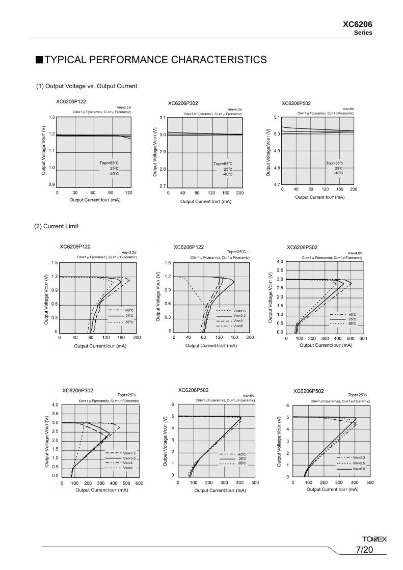
■TYPICAL PERFORMANCE CHARACTERISTICS
(1) Output Voltage vs. Output Current
(2) Current Limit
Topr=25℃
Topr=25℃ Topr=25℃
8/20
XC6206 Series
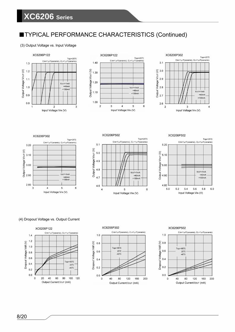
(3) Output Voltage vs. Input Voltage
(4) Dropout Voltage vs. Output Current
■TYPICAL PERFORMANCE CHARACTERISTICS (Continued)
9/20
XC6206Series
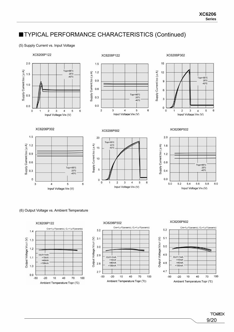
(5) Supply Current vs. Input Voltage
(6) Output Voltage vs. Ambient Temperature
■TYPICAL PERFORMANCE CHARACTERISTICS (Continued)
10/20
XC6206 Series
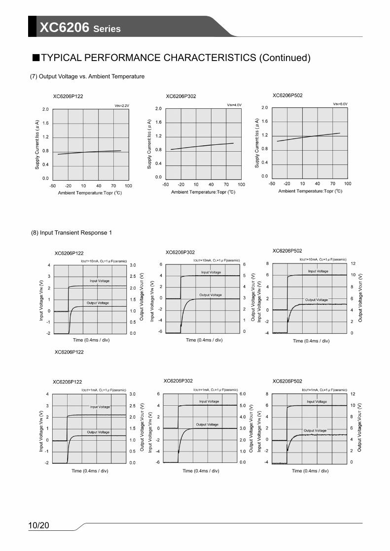
(7) Output Voltage vs. Ambient Temperature
(8) Input Transient Response 1
■TYPICAL PERFORMANCE CHARACTERISTICS (Continued)
Time (0.4ms / div) Time (0.4ms / div) Time (0.4ms / div)
Time (0.4ms / div) Time (0.4ms / div) Time (0.4ms / div)
11/20
XC6206Series
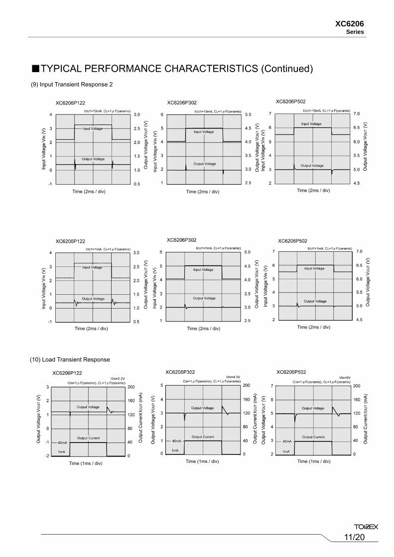
(9) Input Transient Response 2
(10) Load Transient Response
■TYPICAL PERFORMANCE CHARACTERISTICS (Continued)
Time (2ms / div)
Time (2ms / div) Time (2ms / div) Time (2ms / div)
Time (2ms / div) Time (2ms / div)
Time (1ms / div) Time (1ms / div) Time (1ms / div)
12/20
XC6206 Series
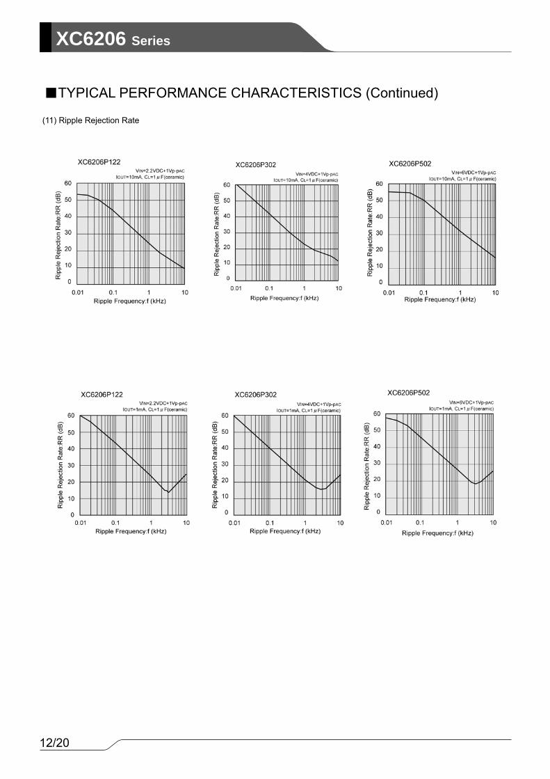
(11) Ripple Rejection Rate
■TYPICAL PERFORMANCE CHARACTERISTICS (Continued)
13/20
XC6206Series
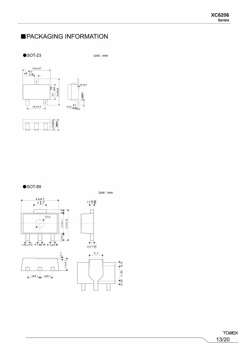
■PACKAGING INFORMATION
●SOT-89
Unit : mm
Unit : mm
2.5±
0.1
4.0±0.25
1.5±0.1
(0.1)
(0.4)
1.0±0.2
(0.4)
(1.85)
(0.25)
●SOT-23
14/20
XC6206 Series
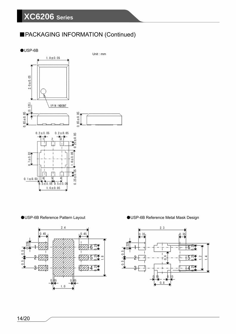
■PACKAGING INFORMATION (Continued)
●USP-6B Reference Pattern Layout ●USP-6B Reference Metal Mask Design
●USP-6B Unit : mm
15/20
XC6206Series
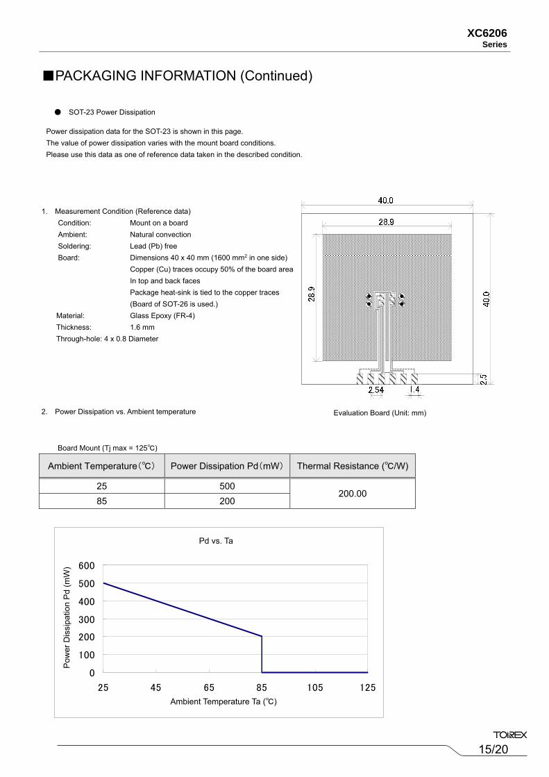
● SOT-23 Power Dissipation
評価基板レイアウト(単位:mm)
Board Mount (Tj max = 125℃)
Ambient Temperature(℃) Power Dissipation Pd(mW) Thermal Resistance (℃/W)
25 500 200.00
85 200
Pd-Ta特性グラフ
0
100
200
300
400
500
600
25 45 65 85 105 125
周囲温度Ta(℃)
許容
損失
Pd(
mW
)■PACKAGING INFORMATION (Continued)
Power dissipation data for the SOT-23 is shown in this page. The value of power dissipation varies with the mount board conditions. Please use this data as one of reference data taken in the described condition.
1. Measurement Condition (Reference data) Condition: Mount on a board Ambient: Natural convection Soldering: Lead (Pb) free Board: Dimensions 40 x 40 mm (1600 mm2 in one side)
Copper (Cu) traces occupy 50% of the board area In top and back faces Package heat-sink is tied to the copper traces (Board of SOT-26 is used.)
Material: Glass Epoxy (FR-4) Thickness: 1.6 mm Through-hole: 4 x 0.8 Diameter
Evaluation Board (Unit: mm) 2. Power Dissipation vs. Ambient temperature
Pd vs. Ta
Ambient Temperature Ta (℃)
Pow
er D
issi
patio
n P
d (m
W)
16/20
XC6206 Series
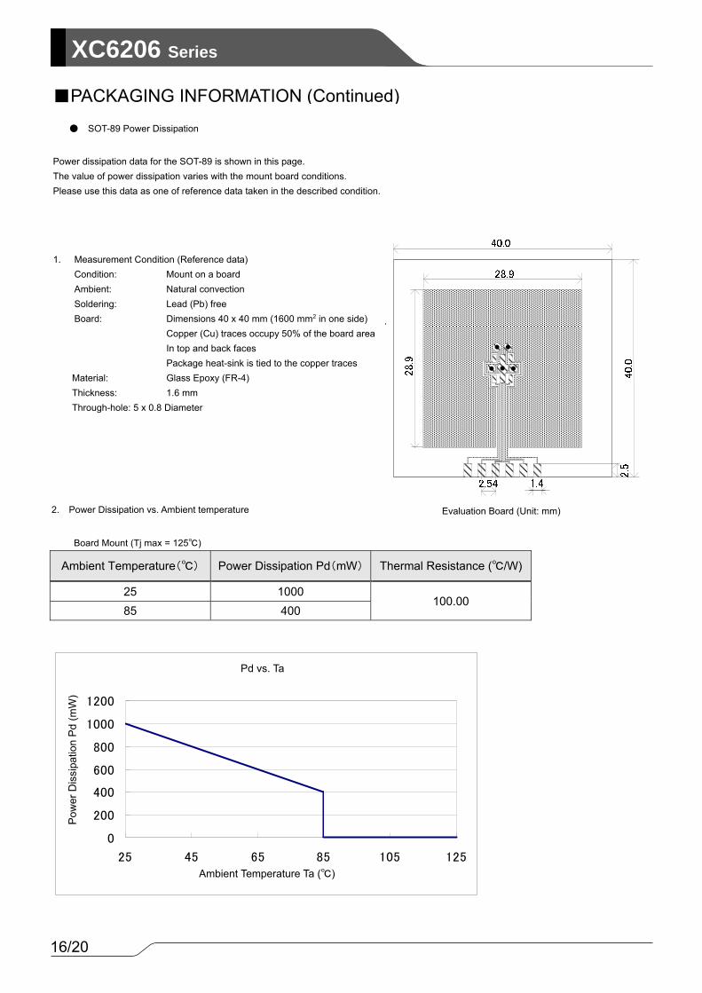
● SOT-89 Power Dissipation
て
Board Mount (Tj max = 125℃)
Ambient Temperature(℃) Power Dissipation Pd(mW) Thermal Resistance (℃/W)
25 1000 100.00
85 400
Pd-Ta特性グラフ
0
200
400
600
800
1000
1200
25 45 65 85 105 125
周囲温度Ta(℃)
許容
損失
Pd(
mW
)
Power dissipation data for the SOT-89 is shown in this page. The value of power dissipation varies with the mount board conditions. Please use this data as one of reference data taken in the described condition.
1. Measurement Condition (Reference data) Condition: Mount on a board Ambient: Natural convection Soldering: Lead (Pb) free Board: Dimensions 40 x 40 mm (1600 mm2 in one side)
Copper (Cu) traces occupy 50% of the board area In top and back faces Package heat-sink is tied to the copper traces
Material: Glass Epoxy (FR-4) Thickness: 1.6 mm Through-hole: 5 x 0.8 Diameter
Evaluation Board (Unit: mm) 2. Power Dissipation vs. Ambient temperature
Pd vs. Ta
Ambient Temperature Ta (℃)
Pow
er D
issi
patio
n P
d (m
W)
■PACKAGING INFORMATION (Continued)
17/20
XC6206Series
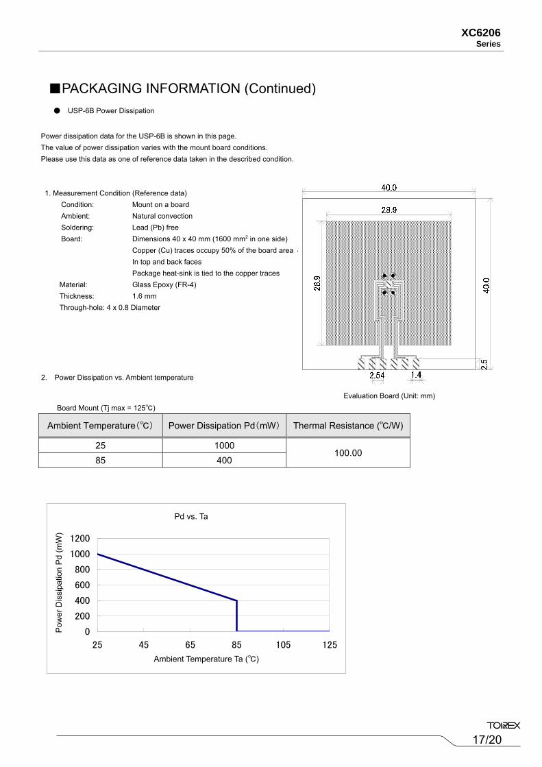
● USP-6B Power Dissipation
て
Board Mount (Tj max = 125℃)
Ambient Temperature(℃) Power Dissipation Pd(mW) Thermal Resistance (℃/W)
25 1000 100.00
85 400
Pd-Ta特性グラフ
0
200
400
600
800
1000
1200
25 45 65 85 105 125
周辺温度Ta(℃)
許容
損失
Pd(
mW
)
■PACKAGING INFORMATION (Continued)
Power dissipation data for the USP-6B is shown in this page. The value of power dissipation varies with the mount board conditions. Please use this data as one of reference data taken in the described condition.
1. Measurement Condition (Reference data) Condition: Mount on a board Ambient: Natural convection Soldering: Lead (Pb) free Board: Dimensions 40 x 40 mm (1600 mm2 in one side)
Copper (Cu) traces occupy 50% of the board area In top and back faces Package heat-sink is tied to the copper traces
Material: Glass Epoxy (FR-4) Thickness: 1.6 mm Through-hole: 4 x 0.8 Diameter
Evaluation Board (Unit: mm)
2. Power Dissipation vs. Ambient temperature
Pd vs. Ta
Ambient Temperature Ta (℃)
Pow
er D
issi
patio
n P
d (m
W)

18/20
XC6206 Series
④③
②①
1 2 3
SOT-89 (TOP VIEW)
① represents product number ② represents 3 pins regulator ③ represents output voltage
MARK VOLTAGE (V) MARK OUTPUT VOLTAGE (V)0 - 3.1 - F 1.6 4.6 - 1 - 3.2 - H 1.7 4.7 - 2 - 3.3 - K 1.8 4.8 - 3 - 3.4 - L 1.9 4.9 - 4 - 3.5 - M 2.0 5.0 - 5 - 3.6 - N 2.1 - - 6 - 3.7 - P 2.2 - - 7 - 3.8 - R 2.3 - - 8 - 3.9 - S 2.4 - - 9 - 4.0 - T 2.5 - - A 4.1 - U 2.6 - - B 1.2 4.2 - V 2.7 - - C 1.3 4.3 - X 2.8 - - D 1.4 4.4 - Y 2.9 - - E 1.5 4.5 - Z 3.0 - -
④ represents production lot number
0 to 9, A to Z, and inverted 0 to 9, A to Z repeated. (G, I, J, O, Q, W excepted.)
MARK PRODUCT SERIES 6 XC6206P*****
MARK PRODUCT SERIES
VOLTAGE=0.1 ~ 3.0V VOLTAGE=3.1 ~ 6.0V 5 6 XC6206P*****
■MARKING RULE ●SOT-23, SOT-89
① ② ③ ④
1 2
3
SOT-23 (TOP VIEW)
19/20
XC6206Series
■MARKING RULE (Continued)
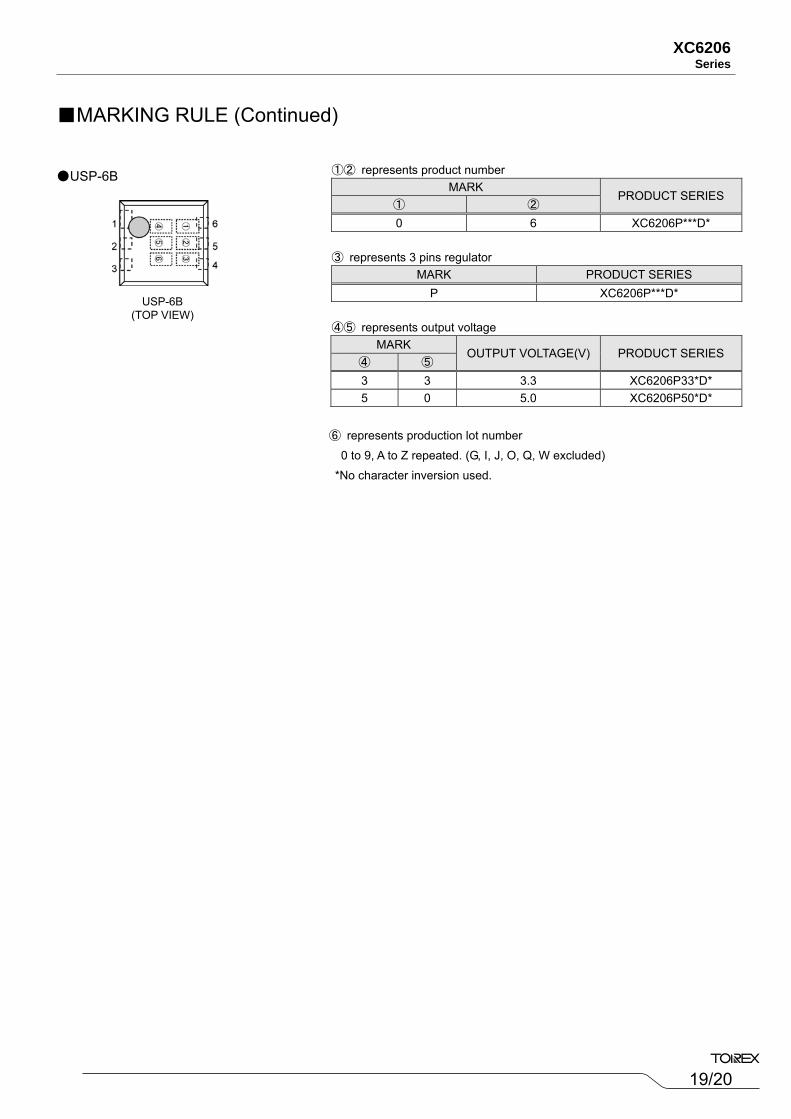
●USP-6B
USP-6B (TOP VIEW)
①② represents product number MARK
PRODUCT SERIES ① ② 0 6 XC6206P***D*
③ represents 3 pins regulator
MARK PRODUCT SERIES P XC6206P***D*
④⑤ represents output voltage
MARK OUTPUT VOLTAGE(V) PRODUCT SERIES
④ ⑤ 3 3 3.3 XC6206P33*D* 5 0 5.0 XC6206P50*D*
⑥ represents production lot number
0 to 9, A to Z repeated. (G, I, J, O, Q, W excluded)
*No character inversion used.
20/20
XC6206 Series
1. The product and product specifications contained herein are subject to change without notice to improve performance characteristics. Consult us, or our representatives before use, to confirm that the information in this datasheet is up to date.
2. The information in this datasheet is intended to illustrate the operation and characteristics of our
products. We neither make warranties or representations with respect to the accuracy or completeness of the information contained in this datasheet nor grant any license to any intellectual property rights of ours or any third party concerning with the information in this datasheet.
3. Applicable export control laws and regulations should be complied and the procedures required by
such laws and regulations should also be followed, when the product or any information contained in this datasheet is exported.
4. The product is neither intended nor warranted for use in equipment of systems which require
extremely high levels of quality and/or reliability and/or a malfunction or failure which may cause loss of human life, bodily injury, serious property damage including but not limited to devices or equipment used in 1) nuclear facilities, 2) aerospace industry, 3) medical facilities, 4) automobile industry and other transportation industry and 5) safety devices and safety equipment to control combustions and explosions. Do not use the product for the above use unless agreed by us in writing in advance.
5. Although we make continuous efforts to improve the quality and reliability of our products;
nevertheless Semiconductors are likely to fail with a certain probability. So in order to prevent personal injury and/or property damage resulting from such failure, customers are required to incorporate adequate safety measures in their designs, such as system fail safes, redundancy and fire prevention features.
6. Our products are not designed to be Radiation-resistant.
7. Please use the product listed in this datasheet within the specified ranges.
8. We assume no responsibility for damage or loss due to abnormal use.
9. All rights reserved. No part of this datasheet may be copied or reproduced unless agreed by Torex
Semiconductor Ltd in writing in advance.
TOREX SEMICONDUCTOR LTD.