Embed Size (px)
Citation preview
70
72
74
76
78
80
82
84
86
88
90
0.1 1 10 100
VI = 5 V
VI = 3.6 V
VI = 2.4 V
Efficiency vs Output Current
IO − Output Current − mA
Eff
icie
ncy
−%
VIN SW
FB
EN GND
L1
10 mH D1
R1
R2
CFF
CO
1 mF
VOUT
VIN to 28 VVIN
1.8 V to 6 V
CIN
4.7 mF
5
4 2
3
1
VO = 18 V
Copyright © 2016, Texas Instruments Incorporated
Product
Folder
Order
Now
Technical
Documents
Tools &
Software
Support &Community
An IMPORTANT NOTICE at the end of this data sheet addresses availability, warranty, changes, use in safety-critical applications,intellectual property matters and other important disclaimers. PRODUCTION DATA.
TPS61040, TPS61041SLVS413J –OCTOBER 2002–REVISED DECEMBER 2019
TPS6104x Low-Power DC-DC Boost Converter in SOT-23 and WSON Packages
1
1 Features1• 1.8-V to 6-V Input Voltage Range• Adjustable Output Voltage Range up to 28 V• 400-mA (TPS61040) and 250-mA (TPS61041)
Internal Switch Current• Up to 1-MHz Switching Frequency• 28-μA Typical No-Load Quiescent Current• 1-μA Typical Shutdown Current• Internal Soft Start• Available in SOT23-5, TSOT23-5,
and 2-mm × 2-mm × 0.8-mm WSON Packages
2 Applications• LCD Bias Supply• White-LED Supply for LCD Backlights• Digital Still Camera• PDAs, Organizers, and Handheld PCs• Cellular Phones• Internet Audio Players• Standard 3.3-V or 5-V to 12-V Conversion
3 DescriptionThe TPS6104x is a high-frequency boost converterdedicated for small to medium LCD bias supply andwhite LED backlight supplies. The device is ideal togenerate output voltages up to 28 V from a dual-cellNiMH/NiCd or a single-cell Li-Ion battery. The partcan also be used to generate standard 3.3-V or 5-Vto 12-V power conversions.
The TPS6104x operates with a switching frequencyup to 1 MHz. This frequency allows the use of smallexternal components using ceramic as well astantalum output capacitors. Together with the thinWSON package, the TPS6104x gives a very smalloverall solution size. The TPS61040 device has aninternal 400-mA switch current limit, while theTPS61041 device has a 250-mA switch current limit,offering lower output voltage ripple and allows theuse of a smaller form factor inductor for lower powerapplications. The low quiescent current (typically 28μA) together with an optimized control scheme,allows device operation at very high efficiencies overthe entire load current range.
Device Information(1)
PART NUMBER PACKAGE BODY SIZE (NOM)
TPS61040SOT-23 (5) 2.90 mm × 1.60 mmSOT (5) 2.90 mm ×1.60 mmWSON (6) 2.00 mm × 2.00 mm
TPS61041SOT-23 (5) 2.90 mm ×1.60 mmWSON (6) 2.00 mm × 2.00 mm
(1) For all available packages, see the orderable addendum atthe end of the datasheet.
Typical Application Schematic
2
TPS61040, TPS61041SLVS413J –OCTOBER 2002–REVISED DECEMBER 2019 www.ti.com
Product Folder Links: TPS61040 TPS61041
Submit Documentation Feedback Copyright © 2002–2019, Texas Instruments Incorporated
Table of Contents1 Features .................................................................. 12 Applications ........................................................... 13 Description ............................................................. 14 Revision History..................................................... 25 Pin Configuration and Functions ......................... 36 Specifications......................................................... 4
6.1 Absolute Maximum Ratings ...................................... 46.2 ESD Ratings.............................................................. 46.3 Recommended Operating Conditions....................... 46.4 Thermal Information .................................................. 46.5 Electrical Characteristics........................................... 56.6 Typical Characteristics .............................................. 6
7 Detailed Description .............................................. 97.1 Overview ................................................................... 97.2 Functional Block Diagram ......................................... 97.3 Feature Description................................................... 97.4 Device Functional Modes........................................ 10
8 Application and Implementation ........................ 118.1 Application Information............................................ 118.2 Typical Application .................................................. 118.3 System Examples ................................................... 16
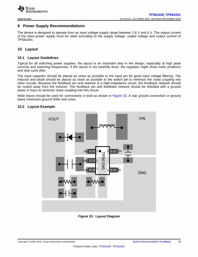
9 Power Supply Recommendations ...................... 1910 Layout................................................................... 19
10.1 Layout Guidelines ................................................. 1910.2 Layout Example .................................................... 19
11 Device and Documentation Support ................. 2011.1 Third-Party Products Disclaimer ........................... 2011.2 Related Links ........................................................ 2011.3 Support Resources ............................................... 2011.4 Trademarks ........................................................... 2011.5 Electrostatic Discharge Caution............................ 2011.6 Glossary ................................................................ 20
12 Mechanical, Packaging, and OrderableInformation ........................................................... 20
4 Revision History
Changes from Revision I (December 2016) to Revision J Page
• Changed DRV package pinout image to show thermal pad outline and transparent top view ............................................. 3
Changes from Revision H (October 2015) to Revision I Page
• Changed CIN from: 4.7 mF To: 4.7 µF and CO From: 1 mF To: 1 µF in the Typical Application Schematic.......................... 1
Changes from Revision G (December 2014) to Revision H Page
• Added 500 µs/div label to X-axis of Figure 15. ................................................................................................................... 15
Changes from Revision F (December 2010) to Revision G Page
• Added ESD Ratings table, Feature Description section, Device Functional Modes, Application and Implementationsection, Power Supply Recommendations section, Layout section, Device and Documentation Support section, andMechanical, Packaging, and Orderable Information section .................................................................................................. 1
GND SW
VIN NC
EN FB3
2
1
4
5
6
Thermal
PAD
3
2
4
51SW
GND
FB
VIN
EN
3
TPS61040, TPS61041www.ti.com SLVS413J –OCTOBER 2002–REVISED DECEMBER 2019
Product Folder Links: TPS61040 TPS61041
Submit Documentation FeedbackCopyright © 2002–2019, Texas Instruments Incorporated
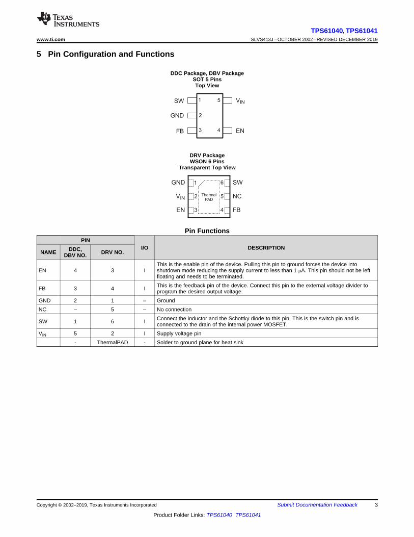
5 Pin Configuration and Functions
DDC Package, DBV PackageSOT 5 PinsTop View
DRV PackageWSON 6 Pins
Transparent Top View
Pin FunctionsPIN
I/O DESCRIPTIONNAME DDC,
DBV NO. DRV NO.
EN 4 3 IThis is the enable pin of the device. Pulling this pin to ground forces the device intoshutdown mode reducing the supply current to less than 1 μA. This pin should not be leftfloating and needs to be terminated.
FB 3 4 I This is the feedback pin of the device. Connect this pin to the external voltage divider toprogram the desired output voltage.
GND 2 1 – GroundNC – 5 – No connection
SW 1 6 I Connect the inductor and the Schottky diode to this pin. This is the switch pin and isconnected to the drain of the internal power MOSFET.
VIN 5 2 I Supply voltage pin- ThermalPAD - Solder to ground plane for heat sink
4
TPS61040, TPS61041SLVS413J –OCTOBER 2002–REVISED DECEMBER 2019 www.ti.com
Product Folder Links: TPS61040 TPS61041
Submit Documentation Feedback Copyright © 2002–2019, Texas Instruments Incorporated
(1) Stresses beyond those listed under Absolute Maximum Ratings may cause permanent damage to the device. These are stress ratingsonly, which do not imply functional operation of the device at these or any other conditions beyond those indicated under RecommendedOperating Conditions. Exposure to absolute-maximum-rated conditions for extended periods may affect device reliability.
(2) All voltage values are with respect to network ground terminal.
6 Specifications
6.1 Absolute Maximum Ratingsover operating free-air temperature range (unless otherwise noted) (1)
MIN MAX UNITSupply voltages on pin VIN
(2) –0.3 7 VVoltages on pins EN, FB (2) –0.3 VIN + 0.3 VSwitch voltage on pin SW (2) 30 30 VOperating junction temperature, TJ –40 150 °CStorage temperature, Tstg –65 150 °C
(1) JEDEC document JEP155 states that 500-V HBM allows safe manufacturing with a standard ESD control process. Manufacturing withless than 500-V HBM is possible with the necessary precautions. Pins listed as ±XXX V may actually have higher performance.
(2) JEDEC document JEP157 states that 250-V CDM allows safe manufacturing with a standard ESD control process. Manufacturing withless than 250-V CDM is possible with the necessary precautions. Pins listed as ±YYY V may actually have higher performance.
6.2 ESD RatingsVALUE UNIT
V(ESD) Electrostatic dischargeHuman body model (HBM), per ANSI/ESDA/JEDEC JS-001 (1) ±2000
VCharged-device model (CDM), per JEDEC specification JESD22-C101 (2)
±750
(1) See application section for further information.
6.3 Recommended Operating ConditionsMIN NOM MAX UNIT
VIN Input voltage range 1.8 6 VVOUT Output voltage range 28 VL Inductor (1) 2.2 10 μHf Switching frequency (1) 1 MHzCIN Input capacitor (1) 4.7 μFCOUT Output capacitor (1) 1 μFTA Operating ambient temperature –40 85 °CTJ Operating junction temperature –40 125 °C
(1) For more information about traditional and new thermal metrics, see the IC Package Thermal Metrics application report, SPRA953.
6.4 Thermal Information
THERMAL METRIC (1)TPS61040 TPS61041
UNITDBV DDC DRV DBV DRV5 PINS 5 PINS 6 PINS 5 PINS 6 PINS
RθJA Junction-to-ambient thermal resistance 205.2 214.7 83.0 205.2 83.0 °C/WRθJC(top) Junction-to-case (top) thermal resistance 118.3 38.5 57.1 118.3 57.1 °C/WRθJB Junction-to-board thermal resistance 34.8 35.4 52.9 34.8 52.9 °C/WψJT Junction-to-top characterization parameter 12.2 0.4 2.4 12.2 2.4 °C/WψJB Junction-to-board characterization parameter 33.9 34.8 53.4 33.9 53.4 °C/WRθJC(bot) Junction-to-case (bottom) thermal resistance — — 26.9 — 26.9 °C/W
5
TPS61040, TPS61041www.ti.com SLVS413J –OCTOBER 2002–REVISED DECEMBER 2019
Product Folder Links: TPS61040 TPS61041
Submit Documentation FeedbackCopyright © 2002–2019, Texas Instruments Incorporated
(1) The line and load regulation depend on the external component selection. See the application section for further information.
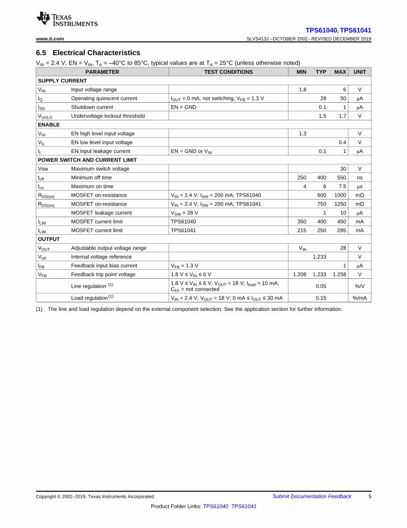
6.5 Electrical CharacteristicsVIN = 2.4 V, EN = VIN, TA = –40°C to 85°C, typical values are at TA = 25°C (unless otherwise noted)
PARAMETER TEST CONDITIONS MIN TYP MAX UNITSUPPLY CURRENTVIN Input voltage range 1.8 6 VIQ Operating quiescent current IOUT = 0 mA, not switching, VFB = 1.3 V 28 50 μAISD Shutdown current EN = GND 0.1 1 μAVUVLO Undervoltage lockout threshold 1.5 1.7 VENABLEVIH EN high level input voltage 1.3 VVIL EN low level input voltage 0.4 VII EN input leakage current EN = GND or VIN 0.1 1 μAPOWER SWITCH AND CURRENT LIMITVsw Maximum switch voltage 30 Vtoff Minimum off time 250 400 550 nston Maximum on time 4 6 7.5 μsRDS(on) MOSFET on-resistance VIN = 2.4 V; ISW = 200 mA; TPS61040 600 1000 mΩRDS(on) MOSFET on-resistance VIN = 2.4 V; ISW = 200 mA; TPS61041 750 1250 mΩ
MOSFET leakage current VSW = 28 V 1 10 μAILIM MOSFET current limit TPS61040 350 400 450 mAILIM MOSFET current limit TPS61041 215 250 285 mAOUTPUTVOUT Adjustable output voltage range VIN 28 VVref Internal voltage reference 1.233 VIFB Feedback input bias current VFB = 1.3 V 1 μAVFB Feedback trip point voltage 1.8 V ≤ VIN ≤ 6 V 1.208 1.233 1.258 V
Line regulation (1) 1.8 V ≤ VIN ≤ 6 V; VOUT = 18 V; Iload = 10 mA;CFF = not connected 0.05 %/V
Load regulation (1) VIN = 2.4 V; VOUT = 18 V; 0 mA ≤ IOUT ≤ 30 mA 0.15 %/mA
70
72
74
76
78
80
82
84
86
88
90
1 2 3 4 5 6
IO = 10 mA
IO = 5 mA
VI − Input Voltage − V
L = 10 µH
VO = 18 V
Eff
icie
ncy −
%
70
72
74
76
78
80
82
84
86
88
90
0.1 1 10 100
L = 10 µH
L = 3.3 µH
IL − Load Current − mA
VO = 18 V
Eff
icie
ncy −
%E
ffic
ien
cy −
%
70
72
74
76
78
80
82
84
86
88
90
0.1 1 10 100
VI = 5 V
VI = 3.6 V
VI = 2.4 V
IO − Output Current − mA
VO = 18 V
70
72
74
76
78
80
82
84
86
88
90
0.1 1 10 100
TPS61040
TPS61041
IL − Load Current − mA
L = 10 µH
VO = 18 V
Eff
icie
ncy −
%
6
TPS61040, TPS61041SLVS413J –OCTOBER 2002–REVISED DECEMBER 2019 www.ti.com
Product Folder Links: TPS61040 TPS61041
Submit Documentation Feedback Copyright © 2002–2019, Texas Instruments Incorporated
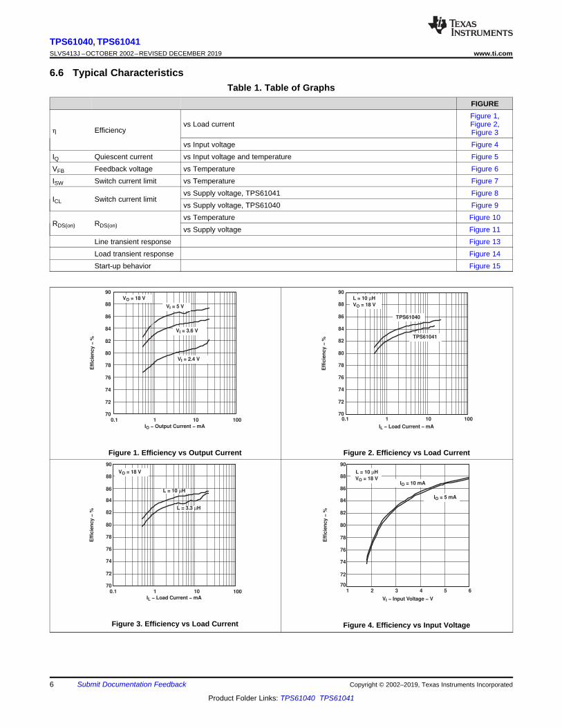
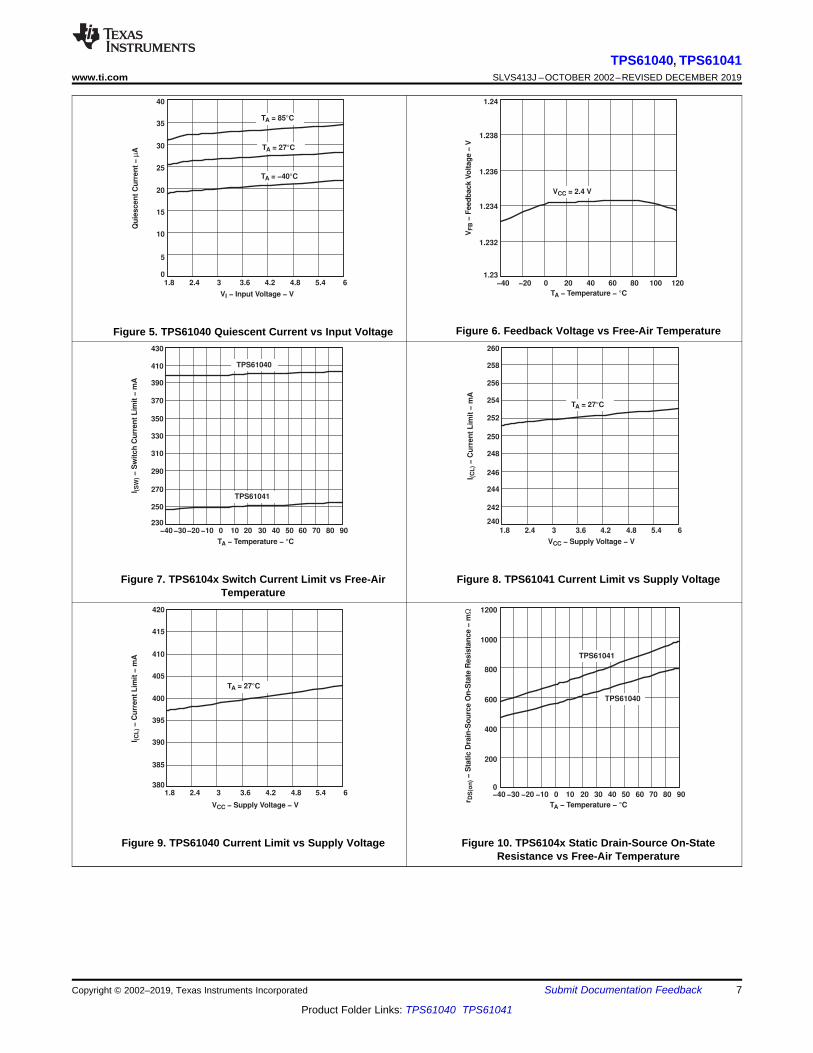
6.6 Typical CharacteristicsTable 1. Table of Graphs
FIGURE
η Efficiencyvs Load current
Figure 1,Figure 2,Figure 3
vs Input voltage Figure 4IQ Quiescent current vs Input voltage and temperature Figure 5VFB Feedback voltage vs Temperature Figure 6ISW Switch current limit vs Temperature Figure 7
ICL Switch current limitvs Supply voltage, TPS61041 Figure 8vs Supply voltage, TPS61040 Figure 9
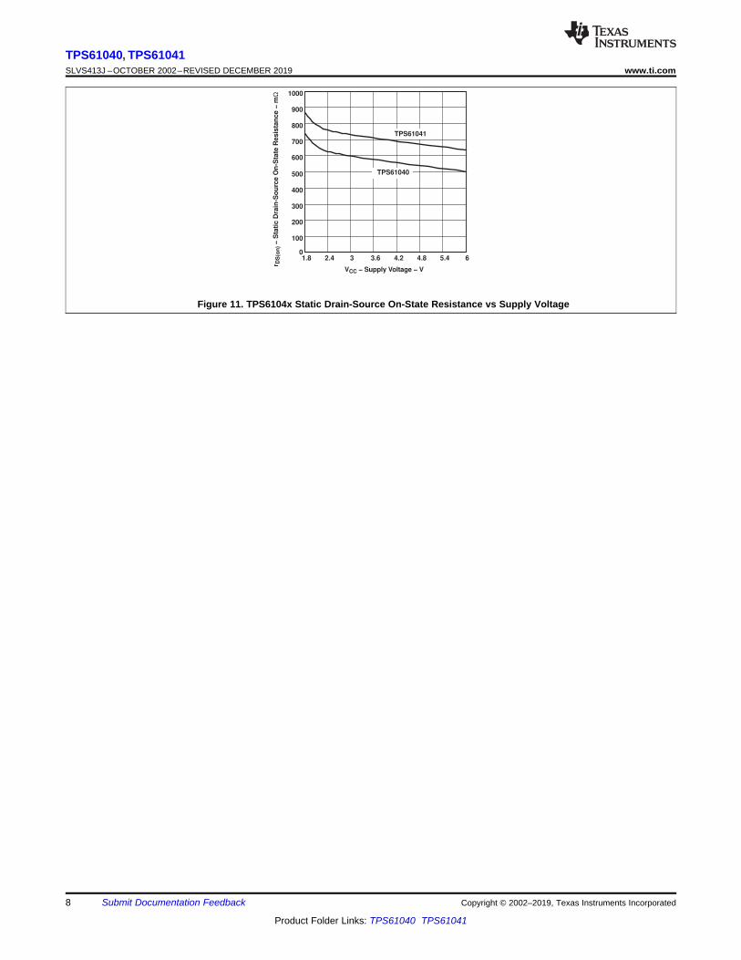
RDS(on) RDS(on)vs Temperature Figure 10vs Supply voltage Figure 11
Line transient response Figure 13Load transient response Figure 14Start-up behavior Figure 15
Figure 1. Efficiency vs Output Current Figure 2. Efficiency vs Load Current
Figure 3. Efficiency vs Load Current Figure 4. Efficiency vs Input Voltage
380
385
390
395
400
405
410
415
420
1.8 2.4 3 3.6 4.2 4.8 5.4 6
VCC − Supply Voltage − V
TA = 27°C
I (C
L) −
Cu
rren
t L
imit
− m
A
0
200
400
600
800
1000
1200
−40 −30 −20 −10 0 10 20 30 40 50 60 70 80 90
TA − Temperature − °C
TPS61041
TPS61040
r DS
(on
) −
Sta
tic D
rain
-So
urc
e O
n-S
tate
Resis
tan
ce −
mΩ
230
250
270
290
310
330
350
370
390
410
430
−40−30−20 −10 0 10 20 30 40 50 60 70 80 90
TPS61040
TPS61041
TA − Temperature − °C
I (S
W) −
Sw
itch
Cu
rren
t L
imit
− m
A
240
242
244
246
248
250
252
254
256
258
260
1.8 2.4 3 3.6 4.2 4.8 5.4 6
VCC − Supply Voltage − V
TA = 27°C
I (C
L) −
Cu
rren
t L
imit
− m
A
0
5
10
15
20
25
30
35
40
1.8 2.4 3 3.6 4.2 4.8 5.4 6
VI − Input Voltage − V
TA = 85°C
TA = 27°C
TA = −40°C
Qu
iescen
t C
urr
en
t −
µA
1.23
1.232
1.234
1.236
1.238
1.24
−40 −20 0 20 40 60 80 100 120
VCC = 2.4 V
TA − Temperature − °C
VF
B −
Feed
back V
olt
ag
e −
V
7
TPS61040, TPS61041www.ti.com SLVS413J –OCTOBER 2002–REVISED DECEMBER 2019
Product Folder Links: TPS61040 TPS61041
Submit Documentation FeedbackCopyright © 2002–2019, Texas Instruments Incorporated
Figure 5. TPS61040 Quiescent Current vs Input Voltage Figure 6. Feedback Voltage vs Free-Air Temperature
Figure 7. TPS6104x Switch Current Limit vs Free-AirTemperature
Figure 8. TPS61041 Current Limit vs Supply Voltage
Figure 9. TPS61040 Current Limit vs Supply Voltage Figure 10. TPS6104x Static Drain-Source On-StateResistance vs Free-Air Temperature
0
100
200
300
400
500
600
700
800
900
1000
1.8 2.4 3 3.6 4.2 4.8 5.4 6
VCC − Supply Voltage − V
TPS61041
TPS61040
r DS
(on
) −
Sta
tic D
rain
-So
urc
e O
n-S
tate
Resis
tan
ce −
mΩ
8
TPS61040, TPS61041SLVS413J –OCTOBER 2002–REVISED DECEMBER 2019 www.ti.com
Product Folder Links: TPS61040 TPS61041
Submit Documentation Feedback Copyright © 2002–2019, Texas Instruments Incorporated
Figure 11. TPS6104x Static Drain-Source On-State Resistance vs Supply Voltage
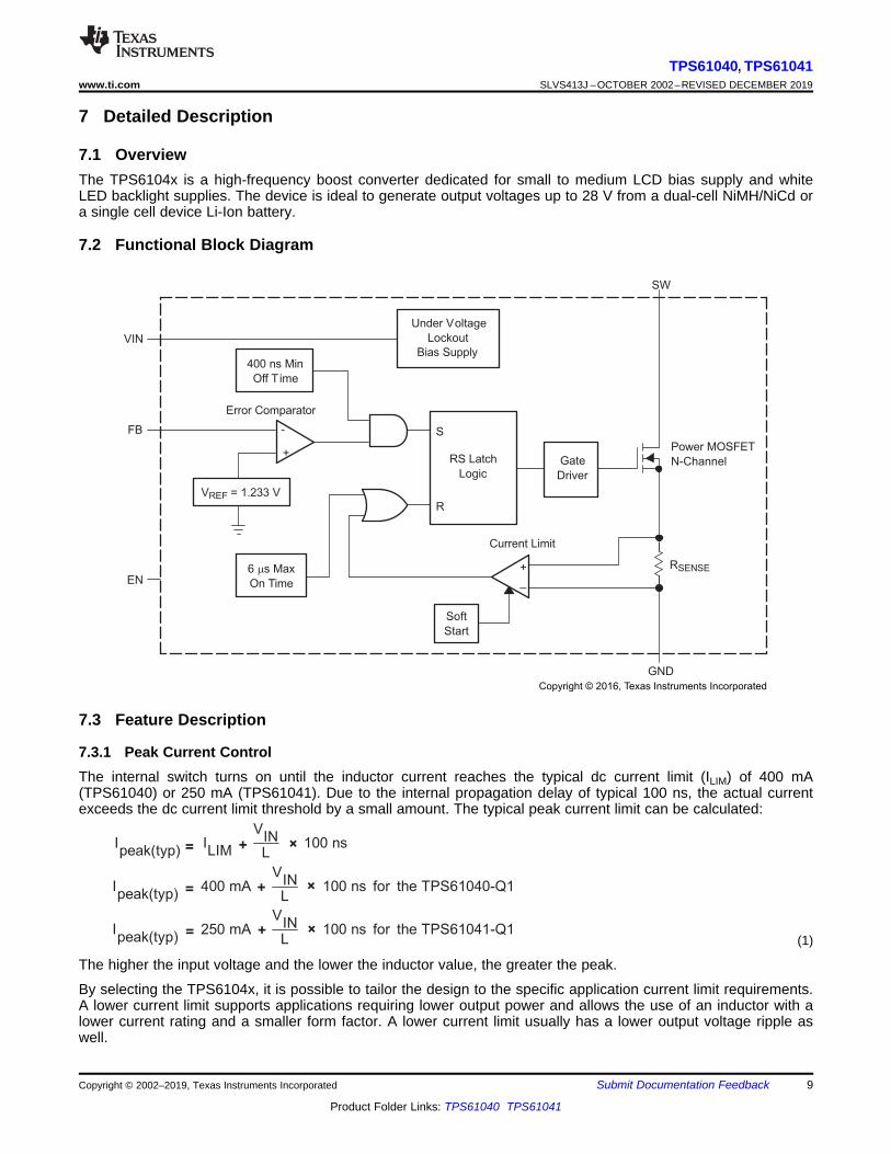
Ipeak(typ)
ILIM
VINL
100 ns
Ipeak(typ)
400 mAV
INL
100 ns for the TPS61040-Q1
Ipeak(typ)
250 mAV
INL
100 ns for the TPS61041-Q1
=
=
=
+
+
+
×
×
×
+
+
-
RS Latch
Logic
S
R
Gate
Driver
_
Current Limit
Power MOSFET
N-Channel
RSENSE
Soft
Start
6 s Maxm
On Time
VREF = 1.233 V
Error Comparator
400 ns Min
Off Time
Under Voltage
Lockout
Bias SupplyVIN
FB
EN
GND
SW
Copyright © 2016, Texas Instruments Incorporated
9
TPS61040, TPS61041www.ti.com SLVS413J –OCTOBER 2002–REVISED DECEMBER 2019
Product Folder Links: TPS61040 TPS61041
Submit Documentation FeedbackCopyright © 2002–2019, Texas Instruments Incorporated
7 Detailed Description
7.1 OverviewThe TPS6104x is a high-frequency boost converter dedicated for small to medium LCD bias supply and whiteLED backlight supplies. The device is ideal to generate output voltages up to 28 V from a dual-cell NiMH/NiCd ora single cell device Li-Ion battery.
7.2 Functional Block Diagram
7.3 Feature Description
7.3.1 Peak Current ControlThe internal switch turns on until the inductor current reaches the typical dc current limit (ILIM) of 400 mA(TPS61040) or 250 mA (TPS61041). Due to the internal propagation delay of typical 100 ns, the actual currentexceeds the dc current limit threshold by a small amount. The typical peak current limit can be calculated:
(1)
The higher the input voltage and the lower the inductor value, the greater the peak.
By selecting the TPS6104x, it is possible to tailor the design to the specific application current limit requirements.A lower current limit supports applications requiring lower output power and allows the use of an inductor with alower current rating and a smaller form factor. A lower current limit usually has a lower output voltage ripple aswell.
ILIM
2
ILIM
4
10
TPS61040, TPS61041SLVS413J –OCTOBER 2002–REVISED DECEMBER 2019 www.ti.com
Product Folder Links: TPS61040 TPS61041
Submit Documentation Feedback Copyright © 2002–2019, Texas Instruments Incorporated
Feature Description (continued)7.3.2 Soft StartAll inductive step-up converters exhibit high inrush current during start-up if no special precaution is made. Thiscan cause voltage drops at the input rail during start up and may result in an unwanted or early system shutdown.
The TPS6104x limits this inrush current by increasing the current limit in two steps starting from for 256
cycles to for the next 256 cycles, and then full current limit (see Figure 15).
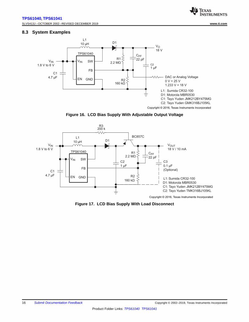
7.3.3 EnablePulling the enable (EN) to ground shuts down the device reducing the shutdown current to 1 μA (typical).Because there is a conductive path from the input to the output through the inductor and Schottky diode, theoutput voltage is equal to the input voltage during shutdown. The enable pin needs to be terminated and shouldnot be left floating. Using a small external transistor disconnects the input from the output during shutdown asshown in Figure 17.
7.3.4 Undervoltage LockoutAn undervoltage lockout prevents misoperation of the device at input voltages below typical 1.5 V. When theinput voltage is below the undervoltage threshold, the main switch is turned off.
7.3.5 Thermal ShutdownAn internal thermal shutdown is implemented and turns off the internal MOSFETs when the typical junctiontemperature of 168°C is exceeded. The thermal shutdown has a hysteresis of typically 25°C. This data is basedon statistical means and is not tested during the regular mass production of the IC.
7.4 Device Functional Modes
7.4.1 OperationThe TPS6104x operates with an input voltage range of 1.8 V to 6 V and can generate output voltages up to 28V. The device operates in a pulse-frequency-modulation (PFM) scheme with constant peak current control. Thiscontrol scheme maintains high efficiency over the entire load current range, and with a switching frequency up to1 MHz, the device enables the use of very small external components.
The converter monitors the output voltage, and as soon as the feedback voltage falls below the reference voltageof typically 1.233 V, the internal switch turns on and the current ramps up. The switch turns off as soon as theinductor current reaches the internally set peak current of typically 400 mA (TPS61040) or 250 mA (TPS61041).See Peak Current Control for more information. The second criteria that turns off the switch is the maximum on-time of 6 μs (typical). This is just to limit the maximum on-time of the converter to cover for extreme conditions.As the switch is turned off the external Schottky diode is forward biased delivering the current to the output. Theswitch remains off for a minimum of 400 ns (typical), or until the feedback voltage drops below the referencevoltage again. Using this PFM peak current control scheme the converter operates in discontinuous conductionmode (DCM) where the switching frequency depends on the output current, which results in very high efficiencyover the entire load current range. This regulation scheme is inherently stable, allowing a wider selection rangefor the inductor and output capacitor.
VIN SW
FB
EN GND
L1
10 μH D1
R12.2 MΩ
R2160 kΩ
CFF
22 pF
C2
1 μF
VOUT
18 VVIN
1.8 V to 6 V
C1
4.7 μF L1: Sumida CR32-100
D1: Motorola MBR0530
C1: Tayo Yuden JMK212BY475MG
C2: Tayo Yuden TMK316BJ105KL
TPS61040
Copyright © 2016, Texas Instruments Incorporated
11
TPS61040, TPS61041www.ti.com SLVS413J –OCTOBER 2002–REVISED DECEMBER 2019
Product Folder Links: TPS61040 TPS61041
Submit Documentation FeedbackCopyright © 2002–2019, Texas Instruments Incorporated
8 Application and Implementation
NOTEInformation in the following applications sections is not part of the TI componentspecification, and TI does not warrant its accuracy or completeness. TI’s customers areresponsible for determining suitability of components for their purposes. Customers shouldvalidate and test their design implementation to confirm system functionality.
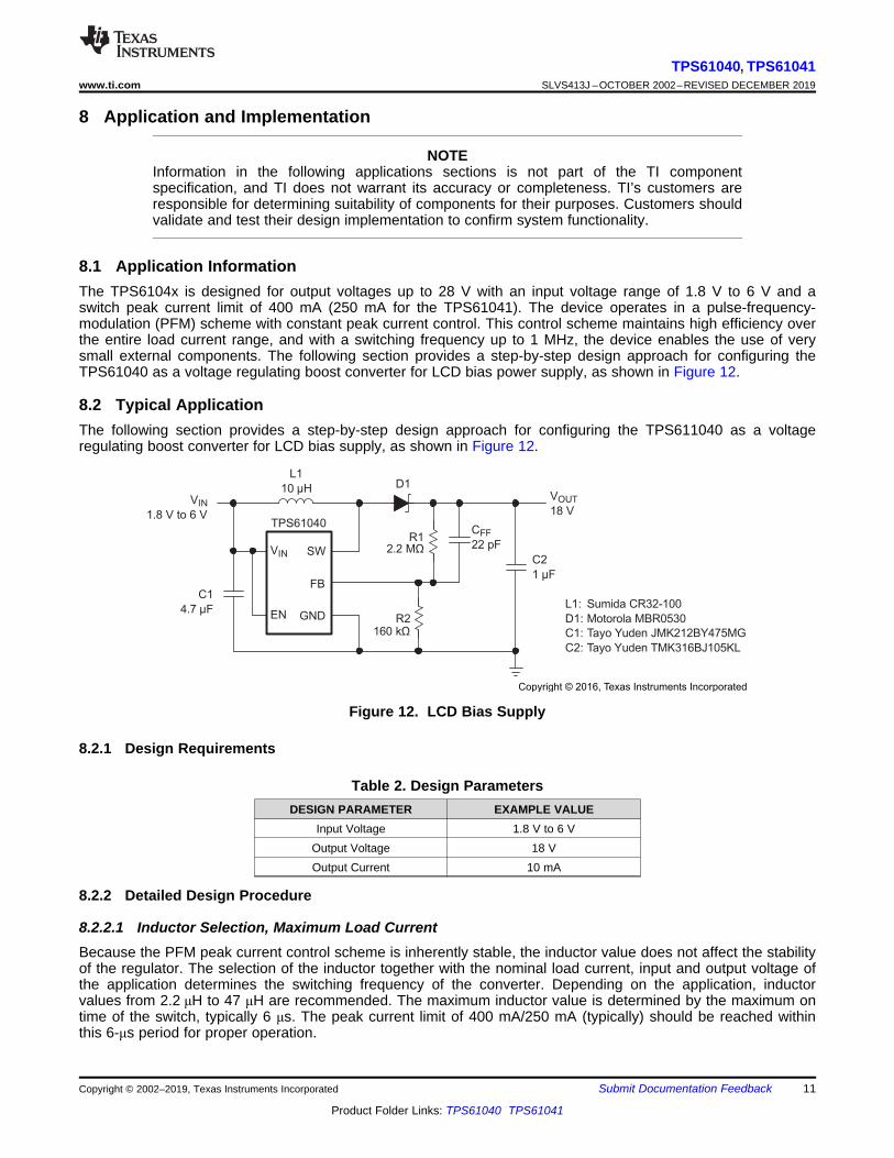
8.1 Application InformationThe TPS6104x is designed for output voltages up to 28 V with an input voltage range of 1.8 V to 6 V and aswitch peak current limit of 400 mA (250 mA for the TPS61041). The device operates in a pulse-frequency-modulation (PFM) scheme with constant peak current control. This control scheme maintains high efficiency overthe entire load current range, and with a switching frequency up to 1 MHz, the device enables the use of verysmall external components. The following section provides a step-by-step design approach for configuring theTPS61040 as a voltage regulating boost converter for LCD bias power supply, as shown in Figure 12.
8.2 Typical ApplicationThe following section provides a step-by-step design approach for configuring the TPS611040 as a voltageregulating boost converter for LCD bias supply, as shown in Figure 12.
Figure 12. LCD Bias Supply
8.2.1 Design Requirements
Table 2. Design ParametersDESIGN PARAMETER EXAMPLE VALUE
Input Voltage 1.8 V to 6 VOutput Voltage 18 VOutput Current 10 mA
8.2.2 Detailed Design Procedure
8.2.2.1 Inductor Selection, Maximum Load CurrentBecause the PFM peak current control scheme is inherently stable, the inductor value does not affect the stabilityof the regulator. The selection of the inductor together with the nominal load current, input and output voltage ofthe application determines the switching frequency of the converter. Depending on the application, inductorvalues from 2.2 μH to 47 μH are recommended. The maximum inductor value is determined by the maximum ontime of the switch, typically 6 μs. The peak current limit of 400 mA/250 mA (typically) should be reached withinthis 6-μs period for proper operation.
2P S(m ax)
load(m ax)O UT IN
I L fI
2 (V V )
´ ´= h
´ -
load OUT IN dS load 2
P
2 I (V V V )f (I )
I L
´ ´ - +
=
´
IN(min) OUT INS(max)
P OUT
V (V V )f
I L V
´ -
=
´ ´
12
TPS61040, TPS61041SLVS413J –OCTOBER 2002–REVISED DECEMBER 2019 www.ti.com
Product Folder Links: TPS61040 TPS61041
Submit Documentation Feedback Copyright © 2002–2019, Texas Instruments Incorporated
The inductor value determines the maximum switching frequency of the converter. Therefore, select the inductorvalue that ensures the maximum switching frequency at the converter maximum load current is not exceeded.The maximum switching frequency is calculated by the following formula:
where• IP = Peak current as described in Peak Current Control• L = Selected inductor value• VIN(min) = The highest switching frequency occurs at the minimum input voltage (2)
If the selected inductor value does not exceed the maximum switching frequency of the converter, the next stepis to calculate the switching frequency at the nominal load current using the following formula:
where• IP = Peak current as described in Peak Current Control• L = Selected inductor value• Iload = Nominal load current• Vd = Rectifier diode forward voltage (typically 0.3 V) (3)
A smaller inductor value gives a higher converter switching frequency, but lowers the efficiency.
The inductor value has less effect on the maximum available load current and is only of secondary order. Thebest way to calculate the maximum available load current under certain operating conditions is to estimate theexpected converter efficiency at the maximum load current. This number can be taken out of the efficiencygraphs shown in Figure 1 through Figure 4. The maximum load current can then be estimated as follows:
where• IP = Peak current as described in Peak Current Control• L = Selected inductor value• fSmax = Maximum switching frequency as calculated previously• η = Expected converter efficiency. Typically 70% to 85% (4)
The maximum load current of the converter is the current at the operation point where the converter starts toenter the continuous conduction mode. Usually the converter should always operate in discontinuous conductionmode.
Last, the selected inductor should have a saturation current that meets the maximum peak current of theconverter (as calculated in Peak Current Control). Use the maximum value for ILIM for this calculation.
Another important inductor parameter is the dc resistance. The lower the dc resistance, the higher the efficiencyof the converter. See Table 3 and the typical applications for the inductor selection.
(1) See Third-Party Products disclaimer
Table 3. Recommended Inductor for Typical LCD Bias Supply (see Figure 23)DEVICE INDUCTOR VALUE COMPONENT SUPPLIER (1) COMMENTS
TPS61040
10 μH Sumida CR32-100 High efficiency10 μH Sumida CDRH3D16-100 High efficiency10 μH Murata LQH4C100K04 High efficiency4.7 μH Sumida CDRH3D16-4R7 Small solution size4.7 μH Murata LQH3C4R7M24 Small solution size
TPS61041 10 μH Murata LQH3C100K24 High efficiencySmall solution size
CFF
1
2 fS
20 R1
VOUT
1.233 V 1 R1
R2
13
TPS61040, TPS61041www.ti.com SLVS413J –OCTOBER 2002–REVISED DECEMBER 2019
Product Folder Links: TPS61040 TPS61041
Submit Documentation FeedbackCopyright © 2002–2019, Texas Instruments Incorporated
8.2.2.2 Setting the Output VoltageThe output voltage is calculated as:
(5)
For battery-powered applications, a high-impedance voltage divider should be used with a typical value for R2 of≤200 kΩ and a maximum value for R1 of 2.2 MΩ. Smaller values might be used to reduce the noise sensitivity ofthe feedback pin.
A feedforward capacitor across the upper feedback resistor R1 is required to provide sufficient overdrive for theerror comparator. Without a feedforward capacitor, or one whose value is too small, the TPS6104x shows doublepulses or a pulse burst instead of single pulses at the switch node (SW), causing higher output voltage ripple. Ifthis higher output voltage ripple is acceptable, the feedforward capacitor can be left out.
The lower the switching frequency of the converter, the larger the feedforward capacitor value required. A goodstarting point is to use a 10-pF feedforward capacitor. As a first estimation, the required value for the feedforwardcapacitor at the operation point can also be calculated using the following formula:
where• R1 = Upper resistor of voltage divider• fS = Switching frequency of the converter at the nominal load current (See Inductor Selection, Maximum Load
Current for calculating the switching frequency)• CFF = Choose a value that comes closest to the result of the calculation (6)
The larger the feedforward capacitor the worse the line regulation of the device. Therefore, when concern for lineregulation is paramount, the selected feedforward capacitor should be as small as possible. See the followingsection for more information about line and load regulation.
8.2.2.3 Line and Load RegulationThe line regulation of the TPS6104x depends on the voltage ripple on the feedback pin. Usually a 50 mV peak-to-peak voltage ripple on the feedback pin FB gives good results.
Some applications require a very tight line regulation and can only allow a small change in output voltage over acertain input voltage range. If no feedforward capacitor CFF is used across the upper resistor of the voltagefeedback divider, the device has the best line regulation. Without the feedforward capacitor the output voltageripple is higher because the TPS6104x shows output voltage bursts instead of single pulses on the switch pin(SW), increasing the output voltage ripple. Increasing the output capacitor value reduces the output voltageripple.
If a larger output capacitor value is not an option, a feed-forward capacitor CFF can be used as described in theprevious section. The use of a feedforward capacitor increases the amount of voltage ripple present on thefeedback pin (FB). The greater the voltage ripple on the feedback pin (≥50 mV), the worse the line regulation.There are two ways to improve the line regulation further:1. Use a smaller inductor value to increase the switching frequency which will lower the output voltage ripple,
as well as the voltage ripple on the feedback pin.2. Add a small capacitor from the feedback pin (FB) to ground to reduce the voltage ripple on the feedback pin
down to 50 mV again. As a starting point, the same capacitor value as selected for the feedforward capacitorCFF can be used.
8.2.2.4 Output Capacitor SelectionFor best output voltage filtering, a low ESR output capacitor is recommended. Ceramic capacitors have a lowESR value but tantalum capacitors can be used as well, depending on the application.
Assuming the converter does not show double pulses or pulse bursts on the switch node (SW), the outputvoltage ripple can be calculated as:
Vout IoutCout
1fS(Iout)
–IP L
Vout Vd–Vin I
P ESR
14
TPS61040, TPS61041SLVS413J –OCTOBER 2002–REVISED DECEMBER 2019 www.ti.com
Product Folder Links: TPS61040 TPS61041
Submit Documentation Feedback Copyright © 2002–2019, Texas Instruments Incorporated
(1) See Third-Party Products disclaimer.
where• IP = Peak current as described in Peak Current Control• L = Selected inductor value• Iout = Nominal load current• fS (Iout) = Switching frequency at the nominal load current as calculated previously• Vd = Rectifier diode forward voltage (typically 0.3 V)• Cout = Selected output capacitor• ESR = Output capacitor ESR value (7)
See Table 4 and the Typical Application for choosing the output capacitor.
Table 4. Recommended Input and Output CapacitorsDEVICE CAPACITOR VOLTAGE RATING COMPONENT SUPPLIER (1) COMMENTS
TPS6104x
4.7 μF/X5R/0805 6.3 V Tayo Yuden JMK212BY475MG CIN/COUT
10 μF/X5R/0805 6.3 V Tayo Yuden JMK212BJ106MG CIN/COUT
1 μF/X7R/1206 25 V Tayo Yuden TMK316BJ105KL COUT
1 μF/X5R/1206 35 V Tayo Yuden GMK316BJ105KL COUT
4.7 μF/X5R/1210 25 V Tayo Yuden TMK325BJ475MG COUT
(1) See Third-Party Products disclaimer.
8.2.2.5 Input Capacitor SelectionFor good input voltage filtering, low ESR ceramic capacitors are recommended. A 4.7-μF ceramic input capacitoris sufficient for most of the applications. For better input voltage filtering this value can be increased. See Table 4and typical applications for input capacitor recommendations.
8.2.2.6 Diode SelectionTo achieve high efficiency a Schottky diode should be used. The current rating of the diode should meet thepeak current rating of the converter as it is calculated in Peak Current Control. Use the maximum value for ILIMfor this calculation. See Table 5 and the typical applications for the selection of the Schottky diode.
Table 5. Recommended Schottky Diode for Typical LCD Bias Supply (see Figure 23)DEVICE REVERSE VOLTAGE COMPONENT SUPPLIER (1) COMMENTS
TPS6104x
30 V ON Semiconductor MBR053020 V ON Semiconductor MBR052020 V ON Semiconductor MBRM120L High efficiency30 V Toshiba CRS02
spacer
VO
5 V/div
EN
1 V/div
II
50 mA/div
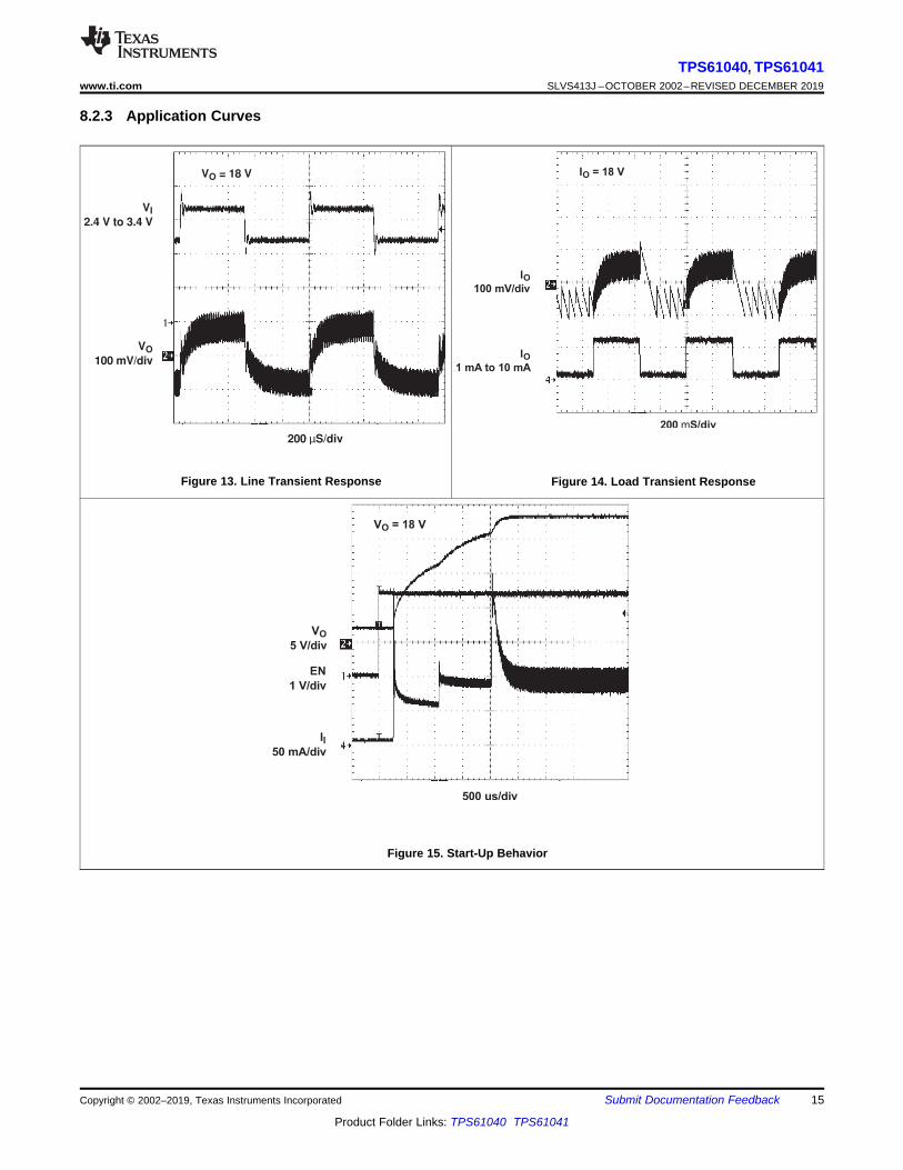
VO = 18 V
500 us/div
VI
2.4 V to 3.4 V
VO
100 mV/div
200 µS/div
VO = 18 V
IO
1 mA to 10 mA
200 mS/div
IO
100 mV/div
IO = 18 V
15
TPS61040, TPS61041www.ti.com SLVS413J –OCTOBER 2002–REVISED DECEMBER 2019
Product Folder Links: TPS61040 TPS61041
Submit Documentation FeedbackCopyright © 2002–2019, Texas Instruments Incorporated
8.2.3 Application Curves
Figure 13. Line Transient Response Figure 14. Load Transient Response
Figure 15. Start-Up Behavior
VIN SW
FB
EN GND
L1
10 μH D1
R12.2 MΩ
R2
160 kΩ
CFF
22 pF
C2
1 μF
VOUT
18 V / 10 mA
VIN
1.8 V to 6 V
C1
4.7 μF
R3200 k
BC857C
C3
0.1 μF
(Optional)
L1: Sumida CR32-100
D1: Motorola MBR0530
C1: Tayo Yuden JMK212BY475MG
C2: Tayo Yuden TMK316BJ105KL
TPS61040
Copyright © 2016, Texas Instruments Incorporated
VIN SW
FB
EN GND
L1
10 μH D1
R12.2 MΩ
R2160 kΩ
CFF
22 pF
C2
1 μF
VO
18 V
VIN
1.8 V to 6 V
C1
4.7 μF DAC or Analog Voltage
0 V = 25 V
1.233 V = 18 V
TPS61040
L1: Sumida CR32-100
D1: Motorola MBR0530
C1: Tayo Yuden JMK212BY475MG
C2: Tayo Yuden GMK316BJ105KL
Copyright © 2016, Texas Instruments Incorporated
16
TPS61040, TPS61041SLVS413J –OCTOBER 2002–REVISED DECEMBER 2019 www.ti.com
Product Folder Links: TPS61040 TPS61041
Submit Documentation Feedback Copyright © 2002–2019, Texas Instruments Incorporated
8.3 System Examples
Figure 16. LCD Bias Supply With Adjustable Output Voltage
Figure 17. LCD Bias Supply With Load Disconnect
VIN SW
FB
EN GND
3.3 μH D1
C2
4.7 μF
5 V/45 mA
1.8 V to 4 V
C1
4.7 μF
TPS61040
L1: Murata LQH4C3R3M04
D1: Motorola MBR0530
C1, C2: Tayo Yuden JMK212BY475MG
CFF
3.3 pFR1
620 kΩ
R2
200 kΩ
Copyright © 2016, Texas Instruments Incorporated
VIN SW
FB
EN GND
L1
6.8 μH D1
R11.8 MΩ
R2205 kΩ
CFF
4.7 pF
C2
4.7 μF
VO = 12 V/35 mA
VIN 3.3 V
C1
10 μF L1: Murata LQH4C6R8M04
D1: Motorola MBR0530
C1: Tayo Yuden JMK212BJ106MG
C2: Tayo Yuden EMK316BJ475ML
TPS61040
Copyright © 2016, Texas Instruments Incorporated
VIN SW
FB
EN GND
L1
6.8 μH D1
R1
1.5 MΩ
R2210 kΩ
CFF
22 pF
C2
1 μF
V1 = 10 V/15 mA
VIN = 2.7 V to 5 V
C1
4.7 μF
C4
4.7 μFC3
1 μF
V2 = –10 V/15 Aμ
D2
D3
L1: Murata LQH4C6R8M04
D1, D2, D3: Motorola MBR0530
C1: Tayo Yuden JMK212BY475MG
C2, C3, C4: Tayo Yuden EMK316BJ105KF
TPS61040
Copyright © 2016, Texas Instruments Incorporated
17
TPS61040, TPS61041www.ti.com SLVS413J –OCTOBER 2002–REVISED DECEMBER 2019
Product Folder Links: TPS61040 TPS61041
Submit Documentation FeedbackCopyright © 2002–2019, Texas Instruments Incorporated
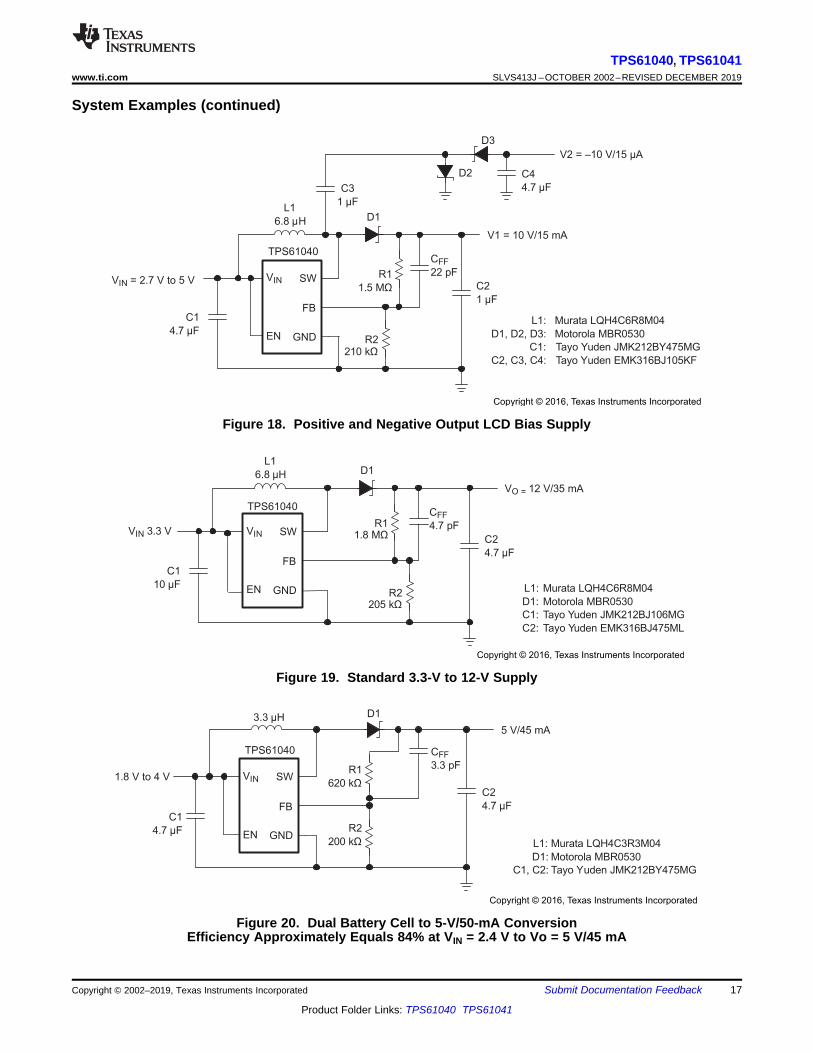
System Examples (continued)
Figure 18. Positive and Negative Output LCD Bias Supply
Figure 19. Standard 3.3-V to 12-V Supply
Figure 20. Dual Battery Cell to 5-V/50-mA ConversionEfficiency Approximately Equals 84% at VIN = 2.4 V to Vo = 5 V/45 mA
VIN SW
FB
EN GND
L1
10 μH
D1
MBRM120L
C2
100 nF
(See
Note A)
C1
4.7 μF
RS
110 Ω
VCC = 2.7 V to 6 V
R1
120 kΩ
R2
160 kΩ
Analog Brightness Control
3.3 V @ Led Off
0 V @Iled = 20 mA
D2
24 V
(Optional)
L1: Murata LQH4C3R3M04
D1: Motorola MBR0530
C1: Tayo Yuden JMK212BY475MG
C2: Standard Ceramic Capacitor
Copyright © 2016, Texas Instruments Incorporated
VIN SW
FB
EN GND
L1
10 μH D1
C2
1 μF
C1
4.7 μF
RS
82 Ω
VCC = 2.7 V to 6 V
PWM
100 Hz to 500 Hz
D2
24 V
(Optional)
L1: Murata LQH4C100K04
D1: Motorola MBR0530
C1: Tayo Yuden JMK212BY475MG
C2: Tayo Yuden TMK316BJ105KL
Copyright © 2016, Texas Instruments Incorporated
18
TPS61040, TPS61041SLVS413J –OCTOBER 2002–REVISED DECEMBER 2019 www.ti.com
Product Folder Links: TPS61040 TPS61041
Submit Documentation Feedback Copyright © 2002–2019, Texas Instruments Incorporated
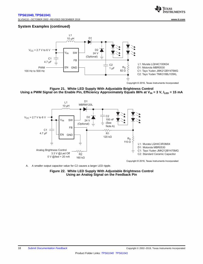
System Examples (continued)
Figure 21. White LED Supply With Adjustable Brightness ControlUsing a PWM Signal on the Enable Pin, Efficiency Approximately Equals 86% at VIN = 3 V, ILED = 15 mA
A. A smaller output capacitor value for C2 causes a larger LED ripple.
Figure 22. White LED Supply With Adjustable Brightness ControlUsing an Analog Signal on the Feedback Pin
VIN1
2
34FB EN
5TP
S61040
SW
GND
VINVOUT
GND
19
TPS61040, TPS61041www.ti.com SLVS413J –OCTOBER 2002–REVISED DECEMBER 2019
Product Folder Links: TPS61040 TPS61041
Submit Documentation FeedbackCopyright © 2002–2019, Texas Instruments Incorporated
9 Power Supply RecommendationsThe device is designed to operate from an input voltage supply range between 1.8 V and 6 V. The output currentof the input power supply must be rated according to the supply voltage, output voltage and output current ofTPS6104x.
10 Layout
10.1 Layout GuidelinesTypical for all switching power supplies, the layout is an important step in the design; especially at high peakcurrents and switching frequencies. If the layout is not carefully done, the regulator might show noise problemsand duty cycle jitter.
The input capacitor should be placed as close as possible to the input pin for good input voltage filtering. Theinductor and diode should be placed as close as possible to the switch pin to minimize the noise coupling intoother circuits. Because the feedback pin and network is a high-impedance circuit, the feedback network shouldbe routed away from the inductor. The feedback pin and feedback network should be shielded with a groundplane or trace to minimize noise coupling into this circuit.
Wide traces should be used for connections in bold as shown in Figure 23. A star ground connection or groundplane minimizes ground shifts and noise.
10.2 Layout Example
Figure 23. Layout Diagram
20
TPS61040, TPS61041SLVS413J –OCTOBER 2002–REVISED DECEMBER 2019 www.ti.com
Product Folder Links: TPS61040 TPS61041
Submit Documentation Feedback Copyright © 2002–2019, Texas Instruments Incorporated
11 Device and Documentation Support
11.1 Third-Party Products DisclaimerTI'S PUBLICATION OF INFORMATION REGARDING THIRD-PARTY PRODUCTS OR SERVICES DOES NOTCONSTITUTE AN ENDORSEMENT REGARDING THE SUITABILITY OF SUCH PRODUCTS OR SERVICESOR A WARRANTY, REPRESENTATION OR ENDORSEMENT OF SUCH PRODUCTS OR SERVICES, EITHERALONE OR IN COMBINATION WITH ANY TI PRODUCT OR SERVICE.
11.2 Related LinksThe table below lists quick access links. Categories include technical documents, support and communityresources, tools and software, and quick access to sample or buy.
Table 6. Related Links
PARTS PRODUCT FOLDER SAMPLE & BUY TECHNICALDOCUMENTS
TOOLS &SOFTWARE
SUPPORT &COMMUNITY
TPS61041 Click here Click here Click here Click here Click hereTPS61040 Click here Click here Click here Click here Click here
11.3 Support ResourcesTI E2E™ support forums are an engineer's go-to source for fast, verified answers and design help — straightfrom the experts. Search existing answers or ask your own question to get the quick design help you need.
Linked content is provided "AS IS" by the respective contributors. They do not constitute TI specifications and donot necessarily reflect TI's views; see TI's Terms of Use.
11.4 TrademarksE2E is a trademark of Texas Instruments.All other trademarks are the property of their respective owners.
11.5 Electrostatic Discharge CautionThese devices have limited built-in ESD protection. The leads should be shorted together or the device placed in conductive foamduring storage or handling to prevent electrostatic damage to the MOS gates.
11.6 GlossarySLYZ022 — TI Glossary.
This glossary lists and explains terms, acronyms, and definitions.
12 Mechanical, Packaging, and Orderable InformationThe following pages include mechanical, packaging, and orderable information. This information is the mostcurrent data available for the designated devices. This data is subject to change without notice and revision ofthis document. For browser-based versions of this data sheet, refer to the left-hand navigation.
PACKAGE OPTION ADDENDUM
www.ti.com 16-Aug-2021
Addendum-Page 1
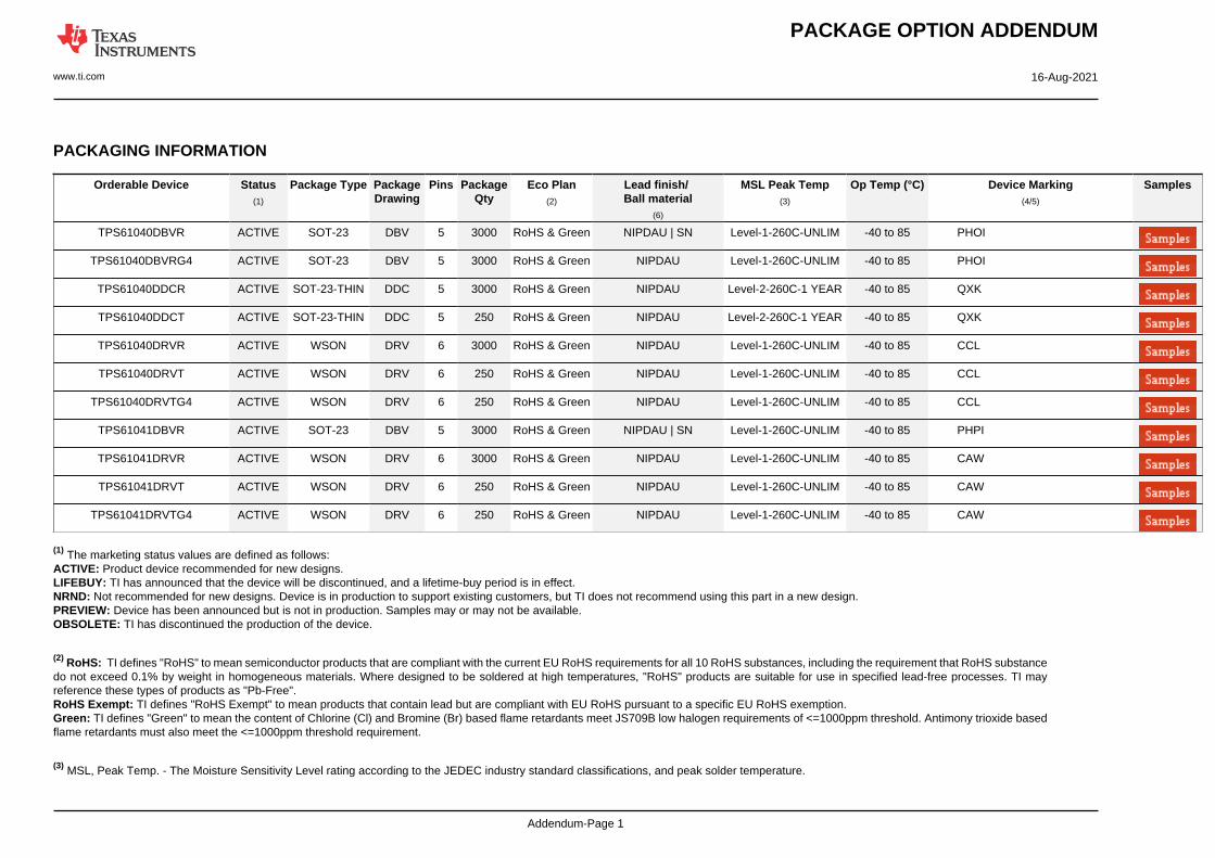
PACKAGING INFORMATION
Orderable Device Status(1)
Package Type PackageDrawing
Pins PackageQty
Eco Plan(2)
Lead finish/Ball material
(6)
MSL Peak Temp(3)
Op Temp (°C) Device Marking(4/5)
Samples
TPS61040DBVR ACTIVE SOT-23 DBV 5 3000 RoHS & Green NIPDAU | SN Level-1-260C-UNLIM -40 to 85 PHOI
TPS61040DBVRG4 ACTIVE SOT-23 DBV 5 3000 RoHS & Green NIPDAU Level-1-260C-UNLIM -40 to 85 PHOI
TPS61040DDCR ACTIVE SOT-23-THIN DDC 5 3000 RoHS & Green NIPDAU Level-2-260C-1 YEAR -40 to 85 QXK
TPS61040DDCT ACTIVE SOT-23-THIN DDC 5 250 RoHS & Green NIPDAU Level-2-260C-1 YEAR -40 to 85 QXK
TPS61040DRVR ACTIVE WSON DRV 6 3000 RoHS & Green NIPDAU Level-1-260C-UNLIM -40 to 85 CCL
TPS61040DRVT ACTIVE WSON DRV 6 250 RoHS & Green NIPDAU Level-1-260C-UNLIM -40 to 85 CCL
TPS61040DRVTG4 ACTIVE WSON DRV 6 250 RoHS & Green NIPDAU Level-1-260C-UNLIM -40 to 85 CCL
TPS61041DBVR ACTIVE SOT-23 DBV 5 3000 RoHS & Green NIPDAU | SN Level-1-260C-UNLIM -40 to 85 PHPI
TPS61041DRVR ACTIVE WSON DRV 6 3000 RoHS & Green NIPDAU Level-1-260C-UNLIM -40 to 85 CAW
TPS61041DRVT ACTIVE WSON DRV 6 250 RoHS & Green NIPDAU Level-1-260C-UNLIM -40 to 85 CAW
TPS61041DRVTG4 ACTIVE WSON DRV 6 250 RoHS & Green NIPDAU Level-1-260C-UNLIM -40 to 85 CAW
(1) The marketing status values are defined as follows:ACTIVE: Product device recommended for new designs.LIFEBUY: TI has announced that the device will be discontinued, and a lifetime-buy period is in effect.NRND: Not recommended for new designs. Device is in production to support existing customers, but TI does not recommend using this part in a new design.PREVIEW: Device has been announced but is not in production. Samples may or may not be available.OBSOLETE: TI has discontinued the production of the device.
(2) RoHS: TI defines "RoHS" to mean semiconductor products that are compliant with the current EU RoHS requirements for all 10 RoHS substances, including the requirement that RoHS substancedo not exceed 0.1% by weight in homogeneous materials. Where designed to be soldered at high temperatures, "RoHS" products are suitable for use in specified lead-free processes. TI mayreference these types of products as "Pb-Free".RoHS Exempt: TI defines "RoHS Exempt" to mean products that contain lead but are compliant with EU RoHS pursuant to a specific EU RoHS exemption.Green: TI defines "Green" to mean the content of Chlorine (Cl) and Bromine (Br) based flame retardants meet JS709B low halogen requirements of <=1000ppm threshold. Antimony trioxide basedflame retardants must also meet the <=1000ppm threshold requirement.
(3) MSL, Peak Temp. - The Moisture Sensitivity Level rating according to the JEDEC industry standard classifications, and peak solder temperature.
PACKAGE OPTION ADDENDUM
www.ti.com 16-Aug-2021
Addendum-Page 2
(4) There may be additional marking, which relates to the logo, the lot trace code information, or the environmental category on the device.
(5) Multiple Device Markings will be inside parentheses. Only one Device Marking contained in parentheses and separated by a "~" will appear on a device. If a line is indented then it is a continuationof the previous line and the two combined represent the entire Device Marking for that device.
(6) Lead finish/Ball material - Orderable Devices may have multiple material finish options. Finish options are separated by a vertical ruled line. Lead finish/Ball material values may wrap to twolines if the finish value exceeds the maximum column width.
Important Information and Disclaimer:The information provided on this page represents TI's knowledge and belief as of the date that it is provided. TI bases its knowledge and belief on informationprovided by third parties, and makes no representation or warranty as to the accuracy of such information. Efforts are underway to better integrate information from third parties. TI has taken andcontinues to take reasonable steps to provide representative and accurate information but may not have conducted destructive testing or chemical analysis on incoming materials and chemicals.TI and TI suppliers consider certain information to be proprietary, and thus CAS numbers and other limited information may not be available for release.
In no event shall TI's liability arising out of such information exceed the total purchase price of the TI part(s) at issue in this document sold by TI to Customer on an annual basis.
OTHER QUALIFIED VERSIONS OF TPS61040, TPS61041 :
• Automotive : TPS61040-Q1, TPS61041-Q1
NOTE: Qualified Version Definitions:
• Automotive - Q100 devices qualified for high-reliability automotive applications targeting zero defects
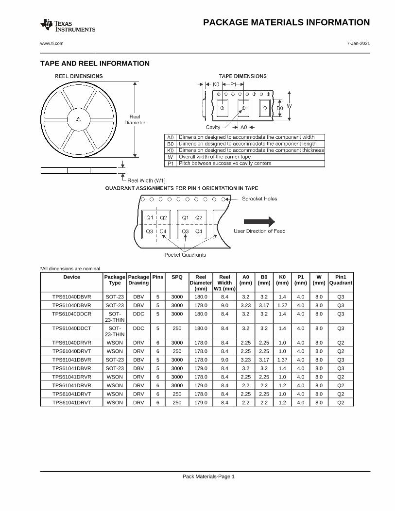
TAPE AND REEL INFORMATION
*All dimensions are nominal
Device PackageType
PackageDrawing
Pins SPQ ReelDiameter
(mm)
ReelWidth
W1 (mm)
A0(mm)
B0(mm)
K0(mm)
P1(mm)
W(mm)
Pin1Quadrant
TPS61040DBVR SOT-23 DBV 5 3000 180.0 8.4 3.2 3.2 1.4 4.0 8.0 Q3
TPS61040DBVR SOT-23 DBV 5 3000 178.0 9.0 3.23 3.17 1.37 4.0 8.0 Q3
TPS61040DDCR SOT-23-THIN
DDC 5 3000 180.0 8.4 3.2 3.2 1.4 4.0 8.0 Q3
TPS61040DDCT SOT-23-THIN
DDC 5 250 180.0 8.4 3.2 3.2 1.4 4.0 8.0 Q3
TPS61040DRVR WSON DRV 6 3000 178.0 8.4 2.25 2.25 1.0 4.0 8.0 Q2
TPS61040DRVT WSON DRV 6 250 178.0 8.4 2.25 2.25 1.0 4.0 8.0 Q2
TPS61041DBVR SOT-23 DBV 5 3000 178.0 9.0 3.23 3.17 1.37 4.0 8.0 Q3
TPS61041DBVR SOT-23 DBV 5 3000 179.0 8.4 3.2 3.2 1.4 4.0 8.0 Q3
TPS61041DRVR WSON DRV 6 3000 178.0 8.4 2.25 2.25 1.0 4.0 8.0 Q2
TPS61041DRVR WSON DRV 6 3000 179.0 8.4 2.2 2.2 1.2 4.0 8.0 Q2
TPS61041DRVT WSON DRV 6 250 178.0 8.4 2.25 2.25 1.0 4.0 8.0 Q2
TPS61041DRVT WSON DRV 6 250 179.0 8.4 2.2 2.2 1.2 4.0 8.0 Q2
PACKAGE MATERIALS INFORMATION
www.ti.com 7-Jan-2021
Pack Materials-Page 1
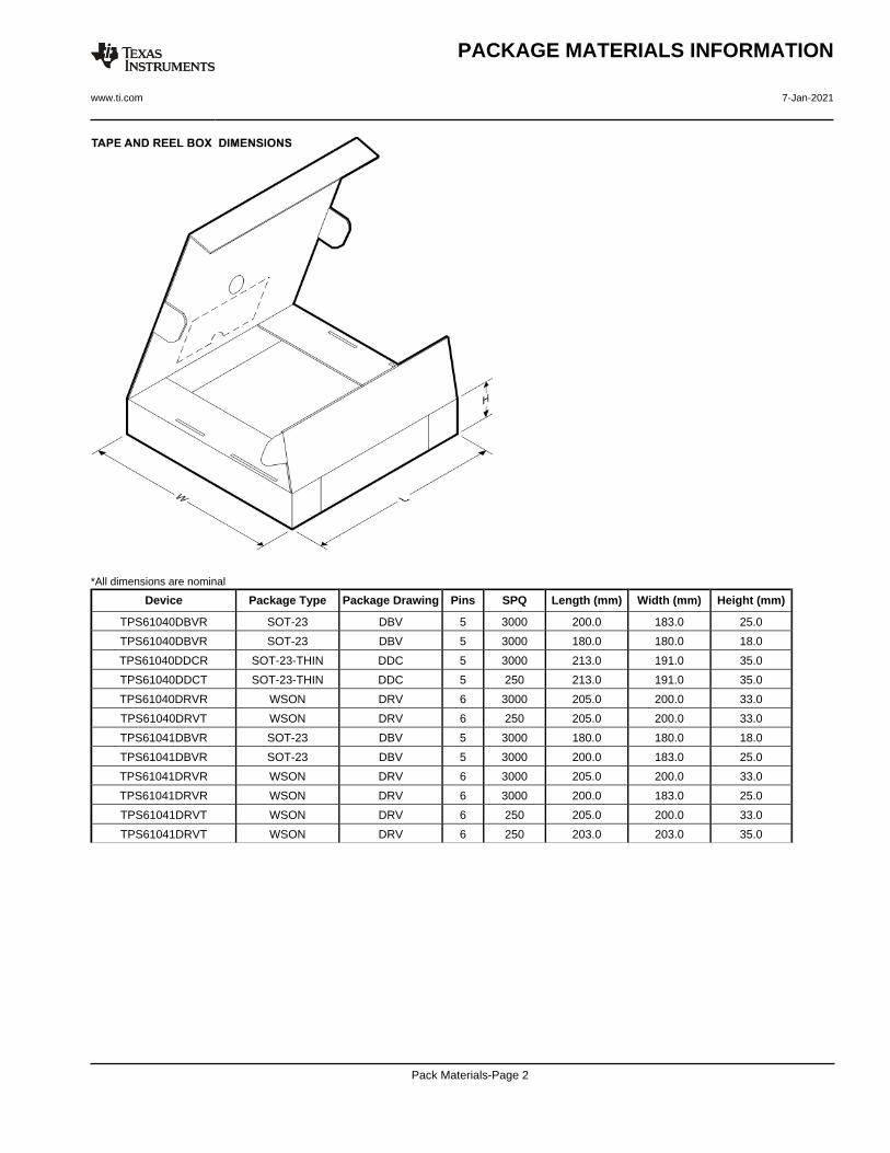
*All dimensions are nominal
Device Package Type Package Drawing Pins SPQ Length (mm) Width (mm) Height (mm)
TPS61040DBVR SOT-23 DBV 5 3000 200.0 183.0 25.0
TPS61040DBVR SOT-23 DBV 5 3000 180.0 180.0 18.0
TPS61040DDCR SOT-23-THIN DDC 5 3000 213.0 191.0 35.0
TPS61040DDCT SOT-23-THIN DDC 5 250 213.0 191.0 35.0
TPS61040DRVR WSON DRV 6 3000 205.0 200.0 33.0
TPS61040DRVT WSON DRV 6 250 205.0 200.0 33.0
TPS61041DBVR SOT-23 DBV 5 3000 180.0 180.0 18.0
TPS61041DBVR SOT-23 DBV 5 3000 200.0 183.0 25.0
TPS61041DRVR WSON DRV 6 3000 205.0 200.0 33.0
TPS61041DRVR WSON DRV 6 3000 200.0 183.0 25.0
TPS61041DRVT WSON DRV 6 250 205.0 200.0 33.0
TPS61041DRVT WSON DRV 6 250 203.0 203.0 35.0
PACKAGE MATERIALS INFORMATION
www.ti.com 7-Jan-2021
Pack Materials-Page 2
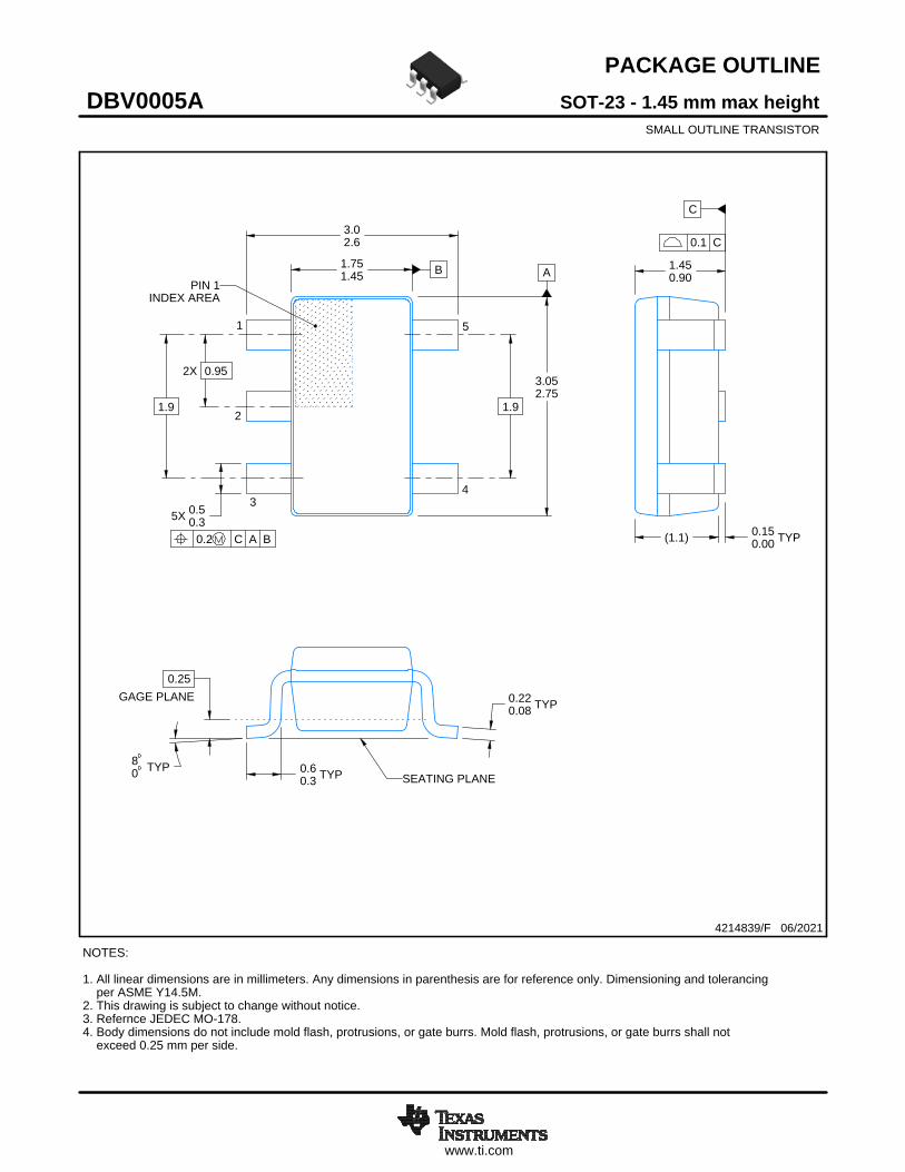
www.ti.com
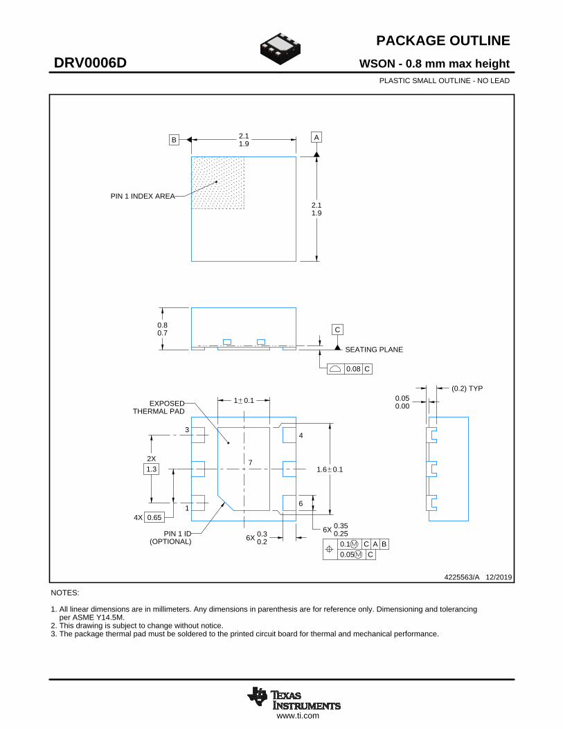
PACKAGE OUTLINE
C
0.220.08 TYP
0.25
3.02.6
2X 0.95
1.9
1.450.90
0.150.00 TYP
5X 0.50.3
0.60.3 TYP
80 TYP
1.9
A
3.052.75
B1.751.45
(1.1)
SOT-23 - 1.45 mm max heightDBV0005ASMALL OUTLINE TRANSISTOR
4214839/F 06/2021
NOTES: 1. All linear dimensions are in millimeters. Any dimensions in parenthesis are for reference only. Dimensioning and tolerancing per ASME Y14.5M.2. This drawing is subject to change without notice.3. Refernce JEDEC MO-178.4. Body dimensions do not include mold flash, protrusions, or gate burrs. Mold flash, protrusions, or gate burrs shall not exceed 0.25 mm per side.
0.2 C A B
1
34
5
2
INDEX AREAPIN 1
GAGE PLANE
SEATING PLANE
0.1 C
SCALE 4.000
www.ti.com
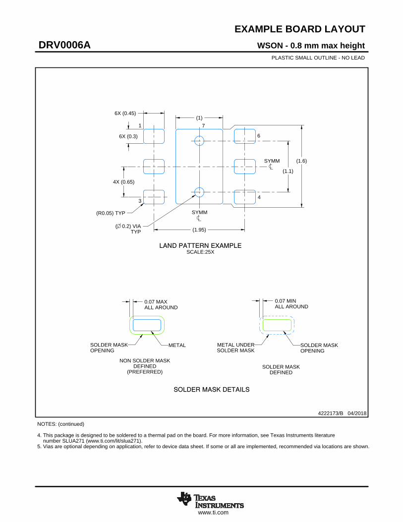
EXAMPLE BOARD LAYOUT
0.07 MAXARROUND
0.07 MINARROUND
5X (1.1)
5X (0.6)
(2.6)
(1.9)
2X (0.95)
(R0.05) TYP
4214839/F 06/2021
SOT-23 - 1.45 mm max heightDBV0005ASMALL OUTLINE TRANSISTOR
NOTES: (continued) 5. Publication IPC-7351 may have alternate designs. 6. Solder mask tolerances between and around signal pads can vary based on board fabrication site.
SYMM
LAND PATTERN EXAMPLEEXPOSED METAL SHOWN
SCALE:15X
PKG
1
3 4
5
2
SOLDER MASKOPENINGMETAL UNDER
SOLDER MASK
SOLDER MASKDEFINED
EXPOSED METAL
METALSOLDER MASKOPENING
NON SOLDER MASKDEFINED
(PREFERRED)
SOLDER MASK DETAILS
EXPOSED METAL
www.ti.com
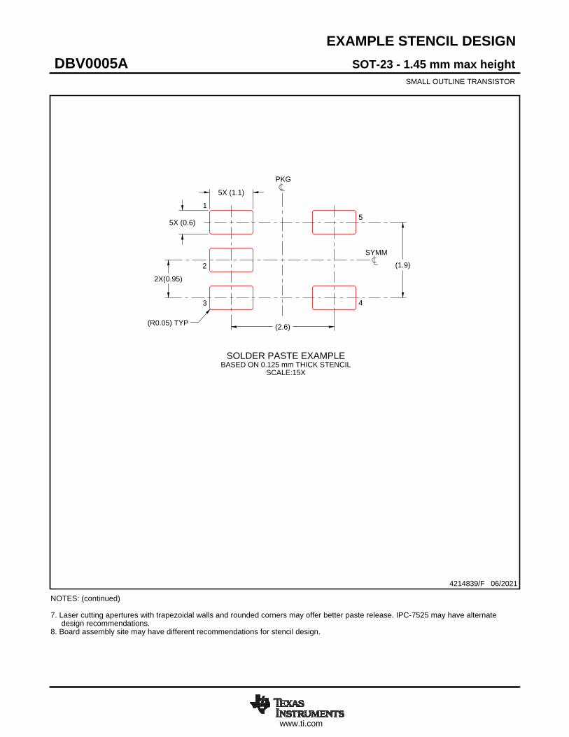
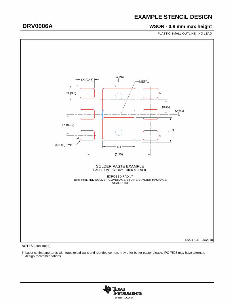
EXAMPLE STENCIL DESIGN
(2.6)
(1.9)
2X(0.95)
5X (1.1)
5X (0.6)
(R0.05) TYP
SOT-23 - 1.45 mm max heightDBV0005ASMALL OUTLINE TRANSISTOR
4214839/F 06/2021
NOTES: (continued) 7. Laser cutting apertures with trapezoidal walls and rounded corners may offer better paste release. IPC-7525 may have alternate design recommendations. 8. Board assembly site may have different recommendations for stencil design.
SOLDER PASTE EXAMPLEBASED ON 0.125 mm THICK STENCIL
SCALE:15X
SYMM
PKG
1
3 4
5
2
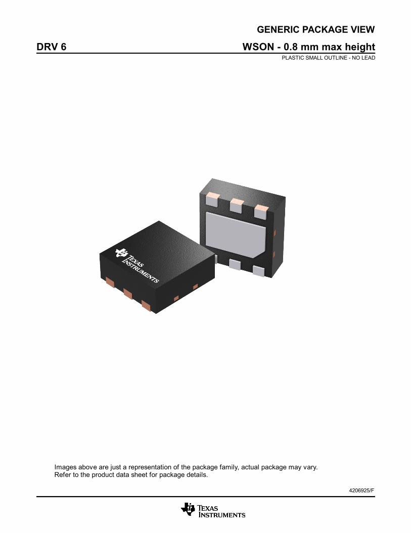
GENERIC PACKAGE VIEW
Images above are just a representation of the package family, actual package may vary.Refer to the product data sheet for package details.
DRV 6 WSON - 0.8 mm max heightPLASTIC SMALL OUTLINE - NO LEAD
4206925/F
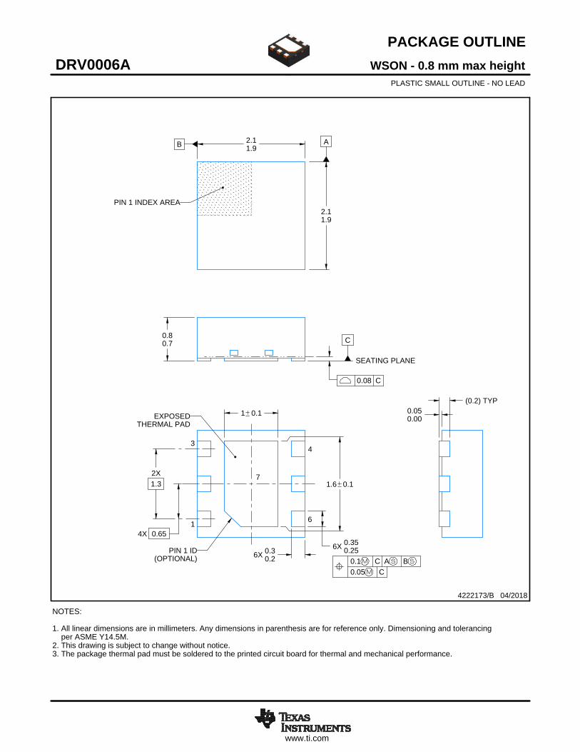
www.ti.com
PACKAGE OUTLINE
C
6X 0.350.25
1.6 0.1
6X 0.30.2
2X1.3
1 0.1
4X 0.65
0.80.7
0.050.00
B 2.11.9
A
2.11.9
(0.2) TYP
WSON - 0.8 mm max heightDRV0006APLASTIC SMALL OUTLINE - NO LEAD
4222173/B 04/2018
PIN 1 INDEX AREA
SEATING PLANE
0.08 C
1
34
6
(OPTIONAL)PIN 1 ID
0.1 C A B0.05 C
THERMAL PADEXPOSED
7
NOTES: 1. All linear dimensions are in millimeters. Any dimensions in parenthesis are for reference only. Dimensioning and tolerancing per ASME Y14.5M. 2. This drawing is subject to change without notice. 3. The package thermal pad must be soldered to the printed circuit board for thermal and mechanical performance.
SCALE 5.500
www.ti.com
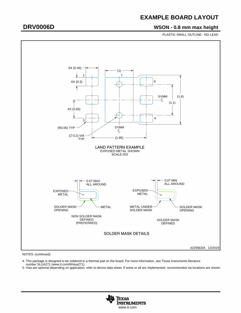
EXAMPLE BOARD LAYOUT
0.07 MINALL AROUND
0.07 MAXALL AROUND
(1)
4X (0.65)
(1.95)
6X (0.3)
6X (0.45)
(1.6)
(R0.05) TYP
( 0.2) VIATYP
(1.1)
WSON - 0.8 mm max heightDRV0006APLASTIC SMALL OUTLINE - NO LEAD
4222173/B 04/2018
SYMM
1
34
6
SYMM
LAND PATTERN EXAMPLESCALE:25X
7
NOTES: (continued) 4. This package is designed to be soldered to a thermal pad on the board. For more information, see Texas Instruments literature number SLUA271 (www.ti.com/lit/slua271).5. Vias are optional depending on application, refer to device data sheet. If some or all are implemented, recommended via locations are shown.
SOLDER MASKOPENINGSOLDER MASK
METAL UNDER
SOLDER MASKDEFINED
METALSOLDER MASKOPENING
SOLDER MASK DETAILS
NON SOLDER MASKDEFINED
(PREFERRED)
www.ti.com
EXAMPLE STENCIL DESIGN
6X (0.3)
6X (0.45)
4X (0.65)
(0.7)
(1)
(1.95)
(R0.05) TYP
(0.45)
WSON - 0.8 mm max heightDRV0006APLASTIC SMALL OUTLINE - NO LEAD
4222173/B 04/2018
NOTES: (continued) 6. Laser cutting apertures with trapezoidal walls and rounded corners may offer better paste release. IPC-7525 may have alternate design recommendations.
SOLDER PASTE EXAMPLEBASED ON 0.125 mm THICK STENCIL
EXPOSED PAD #7
88% PRINTED SOLDER COVERAGE BY AREA UNDER PACKAGESCALE:30X
SYMM
1
3 4
6
SYMM
METAL7
www.ti.com
PACKAGE OUTLINE
C
6X 0.350.25
1.6 0.1
6X 0.30.2
2X1.3
1 0.1
4X 0.65
0.80.7
0.050.00
B 2.11.9
A
2.11.9
(0.2) TYP
WSON - 0.8 mm max heightDRV0006DPLASTIC SMALL OUTLINE - NO LEAD
4225563/A 12/2019
PIN 1 INDEX AREA
SEATING PLANE
0.08 C
1
34
6
(OPTIONAL)PIN 1 ID
0.1 C A B0.05 C
THERMAL PADEXPOSED
7
NOTES: 1. All linear dimensions are in millimeters. Any dimensions in parenthesis are for reference only. Dimensioning and tolerancing per ASME Y14.5M. 2. This drawing is subject to change without notice. 3. The package thermal pad must be soldered to the printed circuit board for thermal and mechanical performance.
SCALE 5.500
www.ti.com
EXAMPLE BOARD LAYOUT
0.07 MINALL AROUND
0.07 MAXALL AROUND
(1)
4X (0.65)
(1.95)
6X (0.3)
6X (0.45)
(1.6)
(R0.05) TYP
( 0.2) VIATYP
(1.1)
WSON - 0.8 mm max heightDRV0006DPLASTIC SMALL OUTLINE - NO LEAD
4225563/A 12/2019
SYMM
1
34
6
SYMM
LAND PATTERN EXAMPLEEXPOSED METAL SHOWN
SCALE:25X
7
NOTES: (continued) 4. This package is designed to be soldered to a thermal pad on the board. For more information, see Texas Instruments literature number SLUA271 (www.ti.com/lit/slua271).5. Vias are optional depending on application, refer to device data sheet. If some or all are implemented, recommended via locations are shown.
SOLDER MASKOPENINGSOLDER MASK
METAL UNDER
SOLDER MASKDEFINED
EXPOSEDMETAL
METALSOLDER MASKOPENING
SOLDER MASK DETAILS
NON SOLDER MASKDEFINED
(PREFERRED)
EXPOSEDMETAL

www.ti.com
EXAMPLE STENCIL DESIGN
6X (0.3)
6X (0.45)
4X (0.65)
(0.7)
(1)
(1.95)
(R0.05) TYP
(0.45)
WSON - 0.8 mm max heightDRV0006DPLASTIC SMALL OUTLINE - NO LEAD
4225563/A 12/2019
NOTES: (continued) 6. Laser cutting apertures with trapezoidal walls and rounded corners may offer better paste release. IPC-7525 may have alternate design recommendations.
SOLDER PASTE EXAMPLEBASED ON 0.125 mm THICK STENCIL
EXPOSED PAD #7
88% PRINTED SOLDER COVERAGE BY AREA UNDER PACKAGESCALE:30X
SYMM
1
3 4
6
SYMM
METAL7

IMPORTANT NOTICE AND DISCLAIMERTI PROVIDES TECHNICAL AND RELIABILITY DATA (INCLUDING DATASHEETS), DESIGN RESOURCES (INCLUDING REFERENCEDESIGNS), APPLICATION OR OTHER DESIGN ADVICE, WEB TOOLS, SAFETY INFORMATION, AND OTHER RESOURCES “AS IS”AND WITH ALL FAULTS, AND DISCLAIMS ALL WARRANTIES, EXPRESS AND IMPLIED, INCLUDING WITHOUT LIMITATION ANYIMPLIED WARRANTIES OF MERCHANTABILITY, FITNESS FOR A PARTICULAR PURPOSE OR NON-INFRINGEMENT OF THIRDPARTY INTELLECTUAL PROPERTY RIGHTS.These resources are intended for skilled developers designing with TI products. You are solely responsible for (1) selecting the appropriateTI products for your application, (2) designing, validating and testing your application, and (3) ensuring your application meets applicablestandards, and any other safety, security, or other requirements. These resources are subject to change without notice. TI grants youpermission to use these resources only for development of an application that uses the TI products described in the resource. Otherreproduction and display of these resources is prohibited. No license is granted to any other TI intellectual property right or to any third partyintellectual property right. TI disclaims responsibility for, and you will fully indemnify TI and its representatives against, any claims, damages,costs, losses, and liabilities arising out of your use of these resources.TI’s products are provided subject to TI’s Terms of Sale (https:www.ti.com/legal/termsofsale.html) or other applicable terms available eitheron ti.com or provided in conjunction with such TI products. TI’s provision of these resources does not expand or otherwise alter TI’sapplicable warranties or warranty disclaimers for TI products.IMPORTANT NOTICE
Mailing Address: Texas Instruments, Post Office Box 655303, Dallas, Texas 75265Copyright © 2021, Texas Instruments Incorporated
![Vol. 2, Issue 9, September 2013 DESIGN OF DC-DC BOOST ... · DESIGN OF DC-DC BOOST CONVERTER WITH THERMOELECTRIC POWER SOURCE ... [2-4].In this research, DC-DC boost converter is](https://img.pdfslide.us/doc/110x75/5aec36db7f8b9ae5318ea3af/vol-2-issue-9-september-2013-design-of-dc-dc-boost-of-dc-dc-boost-converter.jpg)