Embed Size (px)
Citation preview

Data SheetV2.12 2014-06
Microcontrol lers
16/32-BitArchitecture
XC2361A, XC2363A, XC2364A, XC2365A16/32-Bit Single-Chip Microcontroller with 32-Bit PerformanceXC2000 Family / Base Line

Edition 2014-06Published byInfineon Technologies AG81726 Munich, Germany© 2014 Infineon Technologies AGAll Rights Reserved.
Legal DisclaimerThe information given in this document shall in no event be regarded as a guarantee of conditions or characteristics. With respect to any examples or hints given herein, any typical values stated herein and/or any information regarding the application of the device, Infineon Technologies hereby disclaims any and all warranties and liabilities of any kind, including without limitation, warranties of non-infringement of intellectual property rights of any third party.
InformationFor further information on technology, delivery terms and conditions and prices, please contact the nearest Infineon Technologies Office (www.infineon.com).
WarningsDue to technical requirements, components may contain dangerous substances. For information on the types in question, please contact the nearest Infineon Technologies Office.Infineon Technologies components may be used in life-support devices or systems only with the express written approval of Infineon Technologies, if a failure of such components can reasonably be expected to cause the failure of that life-support device or system or to affect the safety or effectiveness of that device or system. Life support devices or systems are intended to be implanted in the human body or to support and/or maintain and sustain and/or protect human life. If they fail, it is reasonable to assume that the health of the user or other persons may be endangered.

Data SheetV2.12 2014-06
Microcontrol lers
16/32-BitArchitecture
XC2361A, XC2363A, XC2364A, XC2365A16/32-Bit Single-Chip Microcontroller with 32-Bit PerformanceXC2000 Family / Base Line

XC2361A, XC2363A, XC2364A, XC2365AXC2000 Family / Base Line
Data Sheet V2.12, 2014-06
TrademarksC166™, TriCore™, and DAVE™ are trademarks of Infineon Technologies AG.
XC236xARevision History: V2.12, 2014-06Previous Version(s):V2.11, 2011-11V2.1, 2011-07V2.0, 2009-03V1.31, 2008-11V1.3, 2008-11V1.2, 2008-09V1.1, 2008-06 PreliminaryV1.0, 2008-06 (Intermediate version)Page Subjects (major changes since last revisions)V2.0 to V2.138 ID registers added85 ADC capacitances corrected (typ. vs. max.)89 Conditions relaxed for ΔfINT
Range for fWU adapted according to PCN 2010-013-AAdded startup time from power-on tSPO
126 Quality declarations addedV2.1 to V2.1114f, 123f Wrong package information (LQFP-144) removedV2.11 to V2.129 Basic device types replaced10 Special device types added14 Logic symbol corrected123 Package type added
We Listen to Your CommentsIs there any information in this document that you feel is wrong, unclear or missing?Your feedback will help us to continuously improve the quality of this document.Please send your proposal (including a reference to this document) to:[email protected]

XC2361A, XC2363A, XC2364A, XC2365AXC2000 Family / Base Line
Table of Contents
Data Sheet 5 V2.12, 2014-06
1 Summary of Features . . . . . . . . . . . . . . . . . . . . . . . . . . . . . . . . . . . . . . . . 71.1 Basic Device Types . . . . . . . . . . . . . . . . . . . . . . . . . . . . . . . . . . . . . . . . . . . 91.2 Special Device Types . . . . . . . . . . . . . . . . . . . . . . . . . . . . . . . . . . . . . . . . 101.3 Definition of Feature Variants . . . . . . . . . . . . . . . . . . . . . . . . . . . . . . . . . . 12
2 General Device Information . . . . . . . . . . . . . . . . . . . . . . . . . . . . . . . . . . 142.1 Pin Configuration and Definition . . . . . . . . . . . . . . . . . . . . . . . . . . . . . . . . 152.2 Identification Registers . . . . . . . . . . . . . . . . . . . . . . . . . . . . . . . . . . . . . . . 38
3 Functional Description . . . . . . . . . . . . . . . . . . . . . . . . . . . . . . . . . . . . . . 393.1 Memory Subsystem and Organization . . . . . . . . . . . . . . . . . . . . . . . . . . . . 403.2 External Bus Controller . . . . . . . . . . . . . . . . . . . . . . . . . . . . . . . . . . . . . . . 433.3 Central Processing Unit (CPU) . . . . . . . . . . . . . . . . . . . . . . . . . . . . . . . . . 443.4 Memory Protection Unit (MPU) . . . . . . . . . . . . . . . . . . . . . . . . . . . . . . . . . 463.5 Memory Checker Module (MCHK) . . . . . . . . . . . . . . . . . . . . . . . . . . . . . . . 463.6 Interrupt System . . . . . . . . . . . . . . . . . . . . . . . . . . . . . . . . . . . . . . . . . . . . 473.7 On-Chip Debug Support (OCDS) . . . . . . . . . . . . . . . . . . . . . . . . . . . . . . . 483.8 Capture/Compare Unit (CAPCOM2) . . . . . . . . . . . . . . . . . . . . . . . . . . . . . 493.9 Capture/Compare Units CCU6x . . . . . . . . . . . . . . . . . . . . . . . . . . . . . . . . 523.10 General Purpose Timer (GPT12E) Unit . . . . . . . . . . . . . . . . . . . . . . . . . . . 543.11 Real Time Clock . . . . . . . . . . . . . . . . . . . . . . . . . . . . . . . . . . . . . . . . . . . . 583.12 A/D Converters . . . . . . . . . . . . . . . . . . . . . . . . . . . . . . . . . . . . . . . . . . . . . 603.13 Universal Serial Interface Channel Modules (USIC) . . . . . . . . . . . . . . . . . 613.14 MultiCAN Module . . . . . . . . . . . . . . . . . . . . . . . . . . . . . . . . . . . . . . . . . . . . 633.15 System Timer . . . . . . . . . . . . . . . . . . . . . . . . . . . . . . . . . . . . . . . . . . . . . . . 643.16 Watchdog Timer . . . . . . . . . . . . . . . . . . . . . . . . . . . . . . . . . . . . . . . . . . . . 653.17 Clock Generation . . . . . . . . . . . . . . . . . . . . . . . . . . . . . . . . . . . . . . . . . . . . 653.18 Parallel Ports . . . . . . . . . . . . . . . . . . . . . . . . . . . . . . . . . . . . . . . . . . . . . . . 663.19 Instruction Set Summary . . . . . . . . . . . . . . . . . . . . . . . . . . . . . . . . . . . . . . 67
4 Electrical Parameters . . . . . . . . . . . . . . . . . . . . . . . . . . . . . . . . . . . . . . . 704.1 General Parameters . . . . . . . . . . . . . . . . . . . . . . . . . . . . . . . . . . . . . . . . . 704.1.1 Absolut Maximum Rating Conditions . . . . . . . . . . . . . . . . . . . . . . . . . . . 704.1.2 Operating Conditions . . . . . . . . . . . . . . . . . . . . . . . . . . . . . . . . . . . . . . . 714.1.3 Pad Timing Definition . . . . . . . . . . . . . . . . . . . . . . . . . . . . . . . . . . . . . . . 734.1.4 Parameter Interpretation . . . . . . . . . . . . . . . . . . . . . . . . . . . . . . . . . . . . 734.2 DC Parameters . . . . . . . . . . . . . . . . . . . . . . . . . . . . . . . . . . . . . . . . . . . . . 744.2.1 DC Parameters . . . . . . . . . . . . . . . . . . . . . . . . . . . . . . . . . . . . . . . . . . . 764.2.2 DC Parameters for Lower Voltage Area . . . . . . . . . . . . . . . . . . . . . . . . 784.2.3 Power Consumption . . . . . . . . . . . . . . . . . . . . . . . . . . . . . . . . . . . . . . . 804.3 Analog/Digital Converter Parameters . . . . . . . . . . . . . . . . . . . . . . . . . . . . 854.4 System Parameters . . . . . . . . . . . . . . . . . . . . . . . . . . . . . . . . . . . . . . . . . . 89
Table of Contents

XC2361A, XC2363A, XC2364A, XC2365AXC2000 Family / Base Line
Table of Contents
Data Sheet 6 V2.12, 2014-06
4.5 Flash Memory Parameters . . . . . . . . . . . . . . . . . . . . . . . . . . . . . . . . . . . . 924.6 AC Parameters . . . . . . . . . . . . . . . . . . . . . . . . . . . . . . . . . . . . . . . . . . . . . 944.6.1 Testing Waveforms . . . . . . . . . . . . . . . . . . . . . . . . . . . . . . . . . . . . . . . . 944.6.2 Definition of Internal Timing . . . . . . . . . . . . . . . . . . . . . . . . . . . . . . . . . . 954.6.2.1 Phase Locked Loop (PLL) . . . . . . . . . . . . . . . . . . . . . . . . . . . . . . . . . 964.6.2.2 Wakeup Clock . . . . . . . . . . . . . . . . . . . . . . . . . . . . . . . . . . . . . . . . . . 994.6.2.3 Selecting and Changing the Operating Frequency . . . . . . . . . . . . . . 994.6.3 External Clock Input Parameters . . . . . . . . . . . . . . . . . . . . . . . . . . . . . 1004.6.4 Pad Properties . . . . . . . . . . . . . . . . . . . . . . . . . . . . . . . . . . . . . . . . . . . 1024.6.5 External Bus Timing . . . . . . . . . . . . . . . . . . . . . . . . . . . . . . . . . . . . . . . 1054.6.5.1 Bus Cycle Control with the READY Input . . . . . . . . . . . . . . . . . . . . 1114.6.6 Synchronous Serial Interface Timing . . . . . . . . . . . . . . . . . . . . . . . . . . 1134.6.7 Debug Interface Timing . . . . . . . . . . . . . . . . . . . . . . . . . . . . . . . . . . . . 117
5 Package and Reliability . . . . . . . . . . . . . . . . . . . . . . . . . . . . . . . . . . . . . 1235.1 Packaging . . . . . . . . . . . . . . . . . . . . . . . . . . . . . . . . . . . . . . . . . . . . . . . . 1235.2 Thermal Considerations . . . . . . . . . . . . . . . . . . . . . . . . . . . . . . . . . . . . . . 1255.3 Quality Declarations . . . . . . . . . . . . . . . . . . . . . . . . . . . . . . . . . . . . . . . . . 126

XC2361A, XC2363A, XC2364A, XC2365AXC2000 Family / Base Line
Summary of Features
Data Sheet 7 V2.12, 2014-06
16/32-Bit Single-Chip Microcontroller with 32-Bit PerformanceXC236xA (XC2000 Family)
1 Summary of FeaturesFor a quick overview and easy reference, the features of the XC236xA are summarizedhere.• High-performance CPU with five-stage pipeline and MPU
– 12.5 ns instruction cycle at 80 MHz CPU clock (single-cycle execution)– One-cycle 32-bit addition and subtraction with 40-bit result– One-cycle multiplication (16 × 16 bit)– Background division (32 / 16 bit) in 21 cycles– One-cycle multiply-and-accumulate (MAC) instructions– Enhanced Boolean bit manipulation facilities– Zero-cycle jump execution– Additional instructions to support HLL and operating systems– Register-based design with multiple variable register banks– Fast context switching support with two additional local register banks– 16 Mbytes total linear address space for code and data– 1024 Bytes on-chip special function register area (C166 Family compatible)– Integrated Memory Protection Unit (MPU)
• Interrupt system with 16 priority levels for up to 96 sources– Selectable external inputs for interrupt generation and wake-up– Fastest sample-rate 12.5 ns
• Eight-channel interrupt-driven single-cycle data transfer withPeripheral Event Controller (PEC), 24-bit pointers cover total address space
• Clock generation from internal or external clock sources,using on-chip PLL or prescaler
• Hardware CRC-Checker with Programmable Polynomial to Supervise On-ChipMemory Areas
• On-chip memory modules– 8 Kbytes on-chip stand-by RAM (SBRAM)– 2 Kbytes on-chip dual-port RAM (DPRAM)– Up to 16 Kbytes on-chip data SRAM (DSRAM)– Up to 32 Kbytes on-chip program/data SRAM (PSRAM)– Up to 832 Kbytes on-chip program memory (Flash memory)– Memory content protection through Error Correction Code (ECC)
• On-Chip Peripheral Modules– Multi-functional general purpose timer unit with 5 timers– 16-channel general purpose capture/compare unit (CAPCOM2)– Two capture/compare units for flexible PWM signal generation (CCU6x)

XC2361A, XC2363A, XC2364A, XC2365AXC2000 Family / Base Line
Summary of Features
Data Sheet 8 V2.12, 2014-06
– Two Synchronizable A/D Converters with a total of up to 16 channels, 10-bitresolution, conversion time below 1 μs, optional data preprocessing (datareduction, range check), broken wire detection
– Up to 6 serial interface channels to be used as UART, LIN, high-speedsynchronous channel (SPI), IIC bus interface (10-bit addressing, 400 kbit/s), IISinterface
– On-chip MultiCAN interface (Rev. 2.0B active) with up to 64 message objects(Full CAN/Basic CAN) on up to 3 CAN nodes and gateway functionality
– On-chip system timer and on-chip real time clock• Up to 12 Mbytes external address space for code and data
– Programmable external bus characteristics for different address ranges– Multiplexed or demultiplexed external address/data buses– Selectable address bus width– 16-bit or 8-bit data bus width– Four programmable chip-select signals
• Single power supply from 3.0 V to 5.5 V• Programmable watchdog timer and oscillator watchdog• Up to 76 general purpose I/O lines• On-chip bootstrap loaders• Supported by a full range of development tools including C compilers, macro-
assembler packages, emulators, evaluation boards, HLL debuggers, simulators,logic analyzer disassemblers, programming boards
• On-chip debug support via Device Access Port (DAP) or JTAG interface• 100-pin Green LQFP package, 0.5 mm (19.7 mil) pitch

XC2361A, XC2363A, XC2364A, XC2365AXC2000 Family / Base Line
Summary of Features
Data Sheet 9 V2.12, 2014-06
Ordering InformationThe ordering code for an Infineon microcontroller provides an exact reference to aspecific product. This ordering code identifies:• the function set of the corresponding product type• the temperature range:
– SAF-…: -40°C to 85°C– SAH-…: -40°C to 110°C– SAK-…: -40°C to 125°C
• the package and the type of delivery.For ordering codes for the XC236xA please contact your sales representative or localdistributor.This document describes several derivatives of the XC236xA group:Basic Device Types are readily available andSpecial Device Types are only available on request.As this document refers to all of these derivatives, some descriptions may not apply to aspecific product, in particular to the special device types.For simplicity the term XC236xA is used for all derivatives throughout this document.
1.1 Basic Device TypesBasic device types are available and can be ordered through Infineon’s direct and/ordistribution channels.
Table 1 Synopsis of XC236xA Basic Device TypesDerivative1)
1) xx is a placeholder for the available speed grade (in MHz).
Flash Memory2)
2) Specific information about the on-chip Flash memory in Table 3.
PSRAMDSRAM3)
3) All derivatives additionally provide 8 Kbytes SBRAM and 2 Kbytes DPRAM.
Capt./Comp. Modules
ADC4) Chan.
4) Specific information about the available channels in Table 5.Analog input channels are listed for each Analog/Digital Converter module separately (ADC0 + ADC1).
Interfaces4)
XC2365A-104FxxLR
832 Kbytes 32 Kbytes16 Kbytes
CC2CCU60/1
11 + 5 3 CAN Nodes,6 Serial Chan.
XC2361A, XC2363A, XC2364A, XC2365AXC2000 Family / Base Line
Summary of Features
Data Sheet 10 V2.12, 2014-06
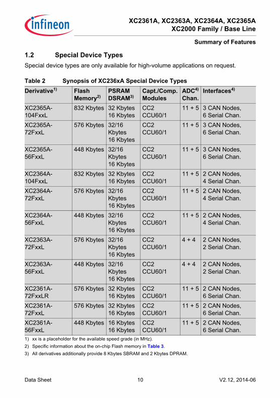
1.2 Special Device TypesSpecial device types are only available for high-volume applications on request.
Table 2 Synopsis of XC236xA Special Device TypesDerivative1)
1) xx is a placeholder for the available speed grade (in MHz).
Flash Memory2)
2) Specific information about the on-chip Flash memory in Table 3.
PSRAMDSRAM3)
3) All derivatives additionally provide 8 Kbytes SBRAM and 2 Kbytes DPRAM.
Capt./Comp. Modules
ADC4) Chan.
Interfaces4)
XC2365A-104FxxL
832 Kbytes 32 Kbytes16 Kbytes
CC2CCU60/1
11 + 5 3 CAN Nodes,6 Serial Chan.
XC2365A-72FxxL
576 Kbytes 32/16 Kbytes16 Kbytes
CC2CCU60/1
11 + 5 3 CAN Nodes,6 Serial Chan.
XC2365A-56FxxL
448 Kbytes 32/16 Kbytes16 Kbytes
CC2CCU60/1
11 + 5 3 CAN Nodes,6 Serial Chan.
XC2364A-104FxxL
832 Kbytes 32 Kbytes16 Kbytes
CC2CCU60/1
11 + 5 2 CAN Nodes,4 Serial Chan.
XC2364A-72FxxL
576 Kbytes 32/16 Kbytes16 Kbytes
CC2CCU60/1
11 + 5 2 CAN Nodes,4 Serial Chan.
XC2364A-56FxxL
448 Kbytes 32/16 Kbytes16 Kbytes
CC2CCU60/1
11 + 5 2 CAN Nodes,4 Serial Chan.
XC2363A-72FxxL
576 Kbytes 32/16 Kbytes16 Kbytes
CC2CCU60/1
4 + 4 2 CAN Nodes,2 Serial Chan.
XC2363A-56FxxL
448 Kbytes 32/16 Kbytes16 Kbytes
CC2CCU60/1
4 + 4 2 CAN Nodes,2 Serial Chan.
XC2361A-72FxxLR
576 Kbytes 32 Kbytes16 Kbytes
CC2CCU60/1
11 + 5 2 CAN Nodes,6 Serial Chan.
XC2361A-72FxxL
576 Kbytes 32 Kbytes16 Kbytes
CC2CCU60/1
11 + 5 2 CAN Nodes,6 Serial Chan.
XC2361A-56FxxL
448 Kbytes 16 Kbytes16 Kbytes
CC2CCU60/1
11 + 5 2 CAN Nodes,6 Serial Chan.

XC2361A, XC2363A, XC2364A, XC2365AXC2000 Family / Base Line
Summary of Features
Data Sheet 11 V2.12, 2014-06
4) Specific information about the available channels in Table 5.Analog input channels are listed for each Analog/Digital Converter module separately (ADC0 + ADC1).

XC2361A, XC2363A, XC2364A, XC2365AXC2000 Family / Base Line
Summary of Features
Data Sheet 12 V2.12, 2014-06
1.3 Definition of Feature VariantsThe XC236xA types are offered with several Flash memory sizes. Table 3 describes thelocation of the available memory areas for each Flash memory size.
The XC236xA types are offered with different interface options. Table 5 lists theavailable channels for each option.
Table 3 Flash Memory AllocationTotal Flash Size Flash Area A1)
1) The uppermost 4-Kbyte sector of the first Flash segment is reserved for internal use (C0’F000H to C0’FFFFH).
Flash Area B Flash Area C832 Kbytes C0’0000H …
C0’EFFFH
C1’0000H … CC’FFFFH
n.a.
576 Kbytes C0’0000H … C0’EFFFH
C1’0000H … C7’FFFFH
CC’0000H … CC’FFFFH
448 Kbytes C0’0000H … C0’EFFFH
C1’0000H … C5’FFFFH
CC’0000H … CC’FFFFH
Table 4 Flash Memory Module Allocation (in Kbytes)Total Flash Size Flash 01)
1) The uppermost 4-Kbyte sector of the first Flash segment is reserved for internal use (C0’F000H to C0’FFFFH).
Flash 1 Flash 2 Flash 3832 Kbytes 256 256 256 64576 Kbytes 256 256 --- 64448 Kbytes 256 128 --- 64
Table 5 Interface Channel AssociationTotal Number Available Channels11 ADC0 channels CH0, CH2 … CH5, CH8 … CH11, CH13, CH154 ADC0 channels CH0, CH2, CH3, CH45 ADC1 channels CH0, CH2, CH4, CH5, CH6 (overlay: CH8 … CH11)4 ADC1 channels CH0, CH2, CH4, CH53 CAN nodes CAN0, CAN1, CAN2
64 message objects2 CAN nodes CAN0, CAN1
64 message objects6 serial channels U0C0, U0C1, U1C0, U1C1, U2C0, U2C1

XC2361A, XC2363A, XC2364A, XC2365AXC2000 Family / Base Line
Summary of Features
Data Sheet 13 V2.12, 2014-06
The XC236xA types are offered with several SRAM memory sizes. Figure 1 shows theallocation rules for PSRAM and DSRAM. Note that the rules differ:• PSRAM allocation starts from the lower address• DSRAM allocation starts from the higher addressFor example 8 Kbytes of PSRAM will be allocated at E0’0000h-E0’1FFFh and 8 Kbytesof DSRAM will be at 00’C000h-00’DFFFh.
Figure 1 SRAM Allocation
4 serial channels U0C0, U0C1, U1C0, U1C12 serial channels U0C0, U0C1
Table 5 Interface Channel Association (cont’d)
Total Number Available Channels
MC_XC_SRAM_ALLOCATION
AvailablePSRAM
Reserved forPSRAM
E0'0000h(E8'0000h)
AvailableDSRAM
Reserved forDSRAM
E7'FFFFh(EF'FFFFh)
00'8000h
00'DFFFh

XC2361A, XC2363A, XC2364A, XC2365AXC2000 Family / Base Line
General Device Information
Data Sheet 14 V2.12, 2014-06
2 General Device InformationThe XC236xA series (16/32-Bit Single-Chip Microcontroller with 32-Bit Performance) isa part of the Infineon XC2000 Family of full-feature single-chip CMOS microcontrollers.These devices extend the functionality and performance of the C166 Family in terms ofinstructions (MAC unit), peripherals, and speed. They combine high CPU performance(up to 80 million instructions per second) with extended peripheral functionality andenhanced IO capabilities. Optimized peripherals can be adapted flexibly to meet theapplication requirements. These derivatives utilize clock generation via PLL and internalor external clock sources. On-chip memory modules include program Flash, programRAM, and data RAM.
Figure 2 XC236xA Logic Symbol
MC_XY_LOGSYMB100
Port 08 bit
Port 18 bit
Port 214 bit
Port 44 bit
Port 63 bit
Port 75 bit
VAGND
(1)VAREF
(1)VDDP
(9)VSS
(4)
JTAG4 bit
TRST Debug2 bit
XTAL1XTAL2ESR0ESR1
Port 1016 bit
Port 155 bit
Port 511 bit
TESTM
PORST
via Port Pins
VDDI1(3)
VDDIM(1)
XC2361A, XC2363A, XC2364A, XC2365AXC2000 Family / Base Line
General Device Information
Data Sheet 15 V2.12, 2014-06
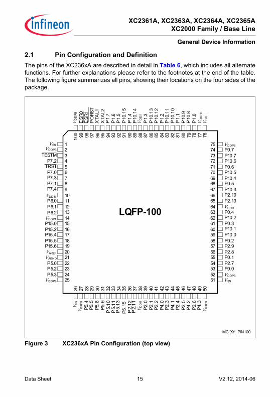
2.1 Pin Configuration and DefinitionThe pins of the XC236xA are described in detail in Table 6, which includes all alternatefunctions. For further explanations please refer to the footnotes at the end of the table.The following figure summarizes all pins, showing their locations on the four sides of thepackage.
Figure 3 XC236xA Pin Configuration (top view)
MC_XY_PIN100
VDDPB 25P5.3 24P5.2 23P5.0 22VAGND 21
2019
P15.5 18
VDDPA
1716
P15.0 15
P15.4
14P6.2 13P6.1 12P6.0 11VDDIM 10
98
P7.3 765
P7.2 4TESTM 3VDDPB 2VSS 1
P7.0TRST
VAREF
P15.6
100 99 98 97 96 95 94 93 92 91 90 89 88 87 86 85 84 83 82 81 80 79 78 77 76
V DD
PB
ESR
0E
SR1
PO
RST
XTA
L1X
TAL2
P1.
7P
1.6
P1.
5P
10.1
5P
1.4
P10
.14
V DD
I1
P1.
3P
10.1
3P
10.1
2P
1.2
P10
.11
P10
.10
P1.
1P
10.9
P10
.8P
1.0
V DD
PBV S
S
26 27 28 29 30 31 32 33 34 35 36 37 38 39 40 41 42 43 44 45P2
.446 47 48 49 50
V SS
V DD
PB
P5.8
P5.9
P5.
10P
5.11
P5.
13P5
.15
P2.
12P
2.11
V DD
I1
P2.0
P2.1
P2.2
P4.0
P2.3
P4.1
P2.5
P4.2
P2.6
P4.3
V DD
PB
75747372717069686766656463626160595857565554535251 VSS
VDDPB
P0.0P2.7P0.1P2.8P2.9P0.2P10.0P10.1
P10.2P0.4VDDI1
P2.13P2.10P10.3P0.5P10.4P10.5P0.6P10.6P10.7P0.7VDDPB
LQFP-100
P7.4P7.1
P15.2P0.3
P5.4
P5.5

XC2361A, XC2363A, XC2364A, XC2365AXC2000 Family / Base Line
General Device Information
Data Sheet 16 V2.12, 2014-06
Key to Pin Definitions• Ctrl.: The output signal for a port pin is selected by bit field PC in the associated
register Px_IOCRy. Output O0 is selected by setting the respective bit field PC to1x00B, output O1 is selected by 1x01B, etc.Output signal OH is controlled by hardware.
• Type: Indicates the pad type and its power supply domain (A, B, M, 1).– St: Standard pad– Sp: Special pad e.g. XTALx– DP: Double pad - can be used as standard or high speed pad– In: Input only pad– PS: Power supply pad
Table 6 Pin Definitions and FunctionsPin Symbol Ctrl. Type Function3 TESTM I In/B Testmode Enable
Enables factory test modes, must be held HIGH for normal operation (connect to VDDPB).An internal pull-up device will hold this pin high when nothing is driving it.
4 P7.2 O0 / I St/B Bit 2 of Port 7, General Purpose Input/OutputEMUX0 O1 St/B External Analog MUX Control Output 0 (ADC1)TDI_C IH St/B JTAG Test Data Input
If JTAG pos. C is selected during start-up, an internal pull-up device will hold this pin high when nothing is driving it.
5 TRST I In/B Test-System Reset InputFor normal system operation, pin TRST should be held low. A high level at this pin at the rising edge of PORST activates the XC236xA’s debug system. In this case, pin TRST must be driven low once to reset the debug system.An internal pull-down device will hold this pin low when nothing is driving it.
XC2361A, XC2363A, XC2364A, XC2365AXC2000 Family / Base Line
General Device Information
Data Sheet 17 V2.12, 2014-06
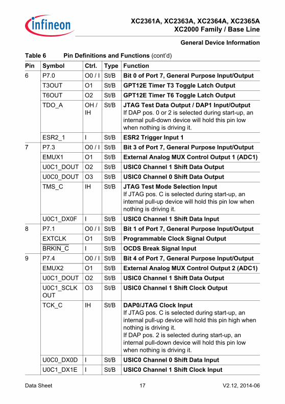
6 P7.0 O0 / I St/B Bit 0 of Port 7, General Purpose Input/OutputT3OUT O1 St/B GPT12E Timer T3 Toggle Latch OutputT6OUT O2 St/B GPT12E Timer T6 Toggle Latch OutputTDO_A OH /
IHSt/B JTAG Test Data Output / DAP1 Input/Output
If DAP pos. 0 or 2 is selected during start-up, an internal pull-down device will hold this pin low when nothing is driving it.
ESR2_1 I St/B ESR2 Trigger Input 17 P7.3 O0 / I St/B Bit 3 of Port 7, General Purpose Input/Output
EMUX1 O1 St/B External Analog MUX Control Output 1 (ADC1)U0C1_DOUT O2 St/B USIC0 Channel 1 Shift Data OutputU0C0_DOUT O3 St/B USIC0 Channel 0 Shift Data OutputTMS_C IH St/B JTAG Test Mode Selection Input
If JTAG pos. C is selected during start-up, an internal pull-up device will hold this pin low when nothing is driving it.
U0C1_DX0F I St/B USIC0 Channel 1 Shift Data Input8 P7.1 O0 / I St/B Bit 1 of Port 7, General Purpose Input/Output
EXTCLK O1 St/B Programmable Clock Signal OutputBRKIN_C I St/B OCDS Break Signal Input
9 P7.4 O0 / I St/B Bit 4 of Port 7, General Purpose Input/OutputEMUX2 O1 St/B External Analog MUX Control Output 2 (ADC1)U0C1_DOUT O2 St/B USIC0 Channel 1 Shift Data OutputU0C1_SCLKOUT
O3 St/B USIC0 Channel 1 Shift Clock Output
TCK_C IH St/B DAP0/JTAG Clock InputIf JTAG pos. C is selected during start-up, an internal pull-up device will hold this pin high when nothing is driving it.If DAP pos. 2 is selected during start-up, an internal pull-down device will hold this pin low when nothing is driving it.
U0C0_DX0D I St/B USIC0 Channel 0 Shift Data InputU0C1_DX1E I St/B USIC0 Channel 1 Shift Clock Input
Table 6 Pin Definitions and Functions (cont’d)
Pin Symbol Ctrl. Type Function

XC2361A, XC2363A, XC2364A, XC2365AXC2000 Family / Base Line
General Device Information
Data Sheet 18 V2.12, 2014-06
11 P6.0 O0 / I DA/A Bit 0 of Port 6, General Purpose Input/OutputEMUX0 O1 DA/A External Analog MUX Control Output 0 (ADC0)TxDC2 O2 DA/A CAN Node 2 Transmit Data OutputBRKOUT O3 DA/A OCDS Break Signal OutputADCx_REQGTyG
I DA/A External Request Gate Input for ADC0/1
U1C1_DX0E I DA/A USIC1 Channel 1 Shift Data Input12 P6.1 O0 / I DA/A Bit 1 of Port 6, General Purpose Input/Output
EMUX1 O1 DA/A External Analog MUX Control Output 1 (ADC0)T3OUT O2 DA/A GPT12E Timer T3 Toggle Latch OutputU1C1_DOUT O3 DA/A USIC1 Channel 1 Shift Data OutputADCx_REQTRyE
I DA/A External Request Trigger Input for ADC0/1
RxDC2E I DA/A CAN Node 2 Receive Data InputESR1_6 I DA/A ESR1 Trigger Input 6
13 P6.2 O0 / I DA/A Bit 2 of Port 6, General Purpose Input/OutputEMUX2 O1 DA/A External Analog MUX Control Output 2 (ADC0)T6OUT O2 DA/A GPT12E Timer T6 Toggle Latch OutputU1C1_SCLKOUT
O3 DA/A USIC1 Channel 1 Shift Clock Output
U1C1_DX1C I DA/A USIC1 Channel 1 Shift Clock Input15 P15.0 I In/A Bit 0 of Port 15, General Purpose Input
ADC1_CH0 I In/A Analog Input Channel 0 for ADC116 P15.2 I In/A Bit 2 of Port 15, General Purpose Input
ADC1_CH2 I In/A Analog Input Channel 2 for ADC1T5INA I In/A GPT12E Timer T5 Count/Gate Input
17 P15.4 I In/A Bit 4 of Port 15, General Purpose InputADC1_CH4 I In/A Analog Input Channel 4 for ADC1T6INA I In/A GPT12E Timer T6 Count/Gate Input
Table 6 Pin Definitions and Functions (cont’d)
Pin Symbol Ctrl. Type Function

XC2361A, XC2363A, XC2364A, XC2365AXC2000 Family / Base Line
General Device Information
Data Sheet 19 V2.12, 2014-06
18 P15.5 I In/A Bit 5 of Port 15, General Purpose InputADC1_CH5 I In/A Analog Input Channel 5 for ADC1T6EUDA I In/A GPT12E Timer T6 External Up/Down Control
Input19 P15.6 I In/A Bit 6 of Port 15, General Purpose Input
ADC1_CH6 I In/A Analog Input Channel 6 for ADC120 VAREF - PS/A Reference Voltage for A/D Converters ADC0/1
21 VAGND - PS/A Reference Ground for A/D Converters ADC0/1
22 P5.0 I In/A Bit 0 of Port 5, General Purpose InputADC0_CH0 I In/A Analog Input Channel 0 for ADC0
23 P5.2 I In/A Bit 2 of Port 5, General Purpose InputADC0_CH2 I In/A Analog Input Channel 2 for ADC0TDI_A I In/A JTAG Test Data Input
24 P5.3 I In/A Bit 3 of Port 5, General Purpose InputADC0_CH3 I In/A Analog Input Channel 3 for ADC0T3INA I In/A GPT12E Timer T3 Count/Gate Input
28 P5.4 I In/A Bit 4 of Port 5, General Purpose InputADC0_CH4 I In/A Analog Input Channel 4 for ADC0T3EUDA I In/A GPT12E Timer T3 External Up/Down Control
InputTMS_A I In/A JTAG Test Mode Selection Input
29 P5.5 I In/A Bit 5 of Port 5, General Purpose InputADC0_CH5 I In/A Analog Input Channel 5 for ADC0CCU60_T12HRB
I In/A External Run Control Input for T12 of CCU60
Table 6 Pin Definitions and Functions (cont’d)
Pin Symbol Ctrl. Type Function

XC2361A, XC2363A, XC2364A, XC2365AXC2000 Family / Base Line
General Device Information
Data Sheet 20 V2.12, 2014-06
30 P5.8 I In/A Bit 8 of Port 5, General Purpose InputADC0_CH8 I In/A Analog Input Channel 8 for ADC0ADC1_CH8 I In/A Analog Input Channel 8 for ADC1CCU6x_T12HRC
I In/A External Run Control Input for T12 of CCU60/1
CCU6x_T13HRC
I In/A External Run Control Input for T13 of CCU60/1
U2C0_DX0F I In/A USIC2 Channel 0 Shift Data Input31 P5.9 I In/A Bit 9 of Port 5, General Purpose Input
ADC0_CH9 I In/A Analog Input Channel 9 for ADC0ADC1_CH9 I In/A Analog Input Channel 9 for ADC1CC2_T7IN I In/A CAPCOM2 Timer T7 Count Input
32 P5.10 I In/A Bit 10 of Port 5, General Purpose InputADC0_CH10 I In/A Analog Input Channel 10 for ADC0ADC1_CH10 I In/A Analog Input Channel 10 for ADC1BRKIN_A I In/A OCDS Break Signal InputU2C1_DX0F I In/A USIC2 Channel 1 Shift Data InputCCU61_T13HRA
I In/A External Run Control Input for T13 of CCU61
33 P5.11 I In/A Bit 11 of Port 5, General Purpose InputADC0_CH11 I In/A Analog Input Channel 11 for ADC0ADC1_CH11 I In/A Analog Input Channel 11 for ADC1
34 P5.13 I In/A Bit 13 of Port 5, General Purpose InputADC0_CH13 I In/A Analog Input Channel 13 for ADC0
35 P5.15 I In/A Bit 15 of Port 5, General Purpose InputADC0_CH15 I In/A Analog Input Channel 15 for ADC0RxDC2F I In/A CAN Node 2 Receive Data Input
Table 6 Pin Definitions and Functions (cont’d)
Pin Symbol Ctrl. Type Function

XC2361A, XC2363A, XC2364A, XC2365AXC2000 Family / Base Line
General Device Information
Data Sheet 21 V2.12, 2014-06
36 P2.12 O0 / I St/B Bit 12 of Port 2, General Purpose Input/OutputU0C0_SELO4
O1 St/B USIC0 Channel 0 Select/Control 4 Output
U0C1_SELO3
O2 St/B USIC0 Channel 1 Select/Control 3 Output
TXDC2 O3 St/B CAN Node 2 Transmit Data OutputREADY IH St/B External Bus Interface READY Input
37 P2.11 O0 / I St/B Bit 11 of Port 2, General Purpose Input/OutputU0C0_SELO2
O1 St/B USIC0 Channel 0 Select/Control 2 Output
U0C1_SELO2
O2 St/B USIC0 Channel 1 Select/Control 2 Output
BHE/WRH OH St/B External Bus Interf. High-Byte Control OutputCan operate either as Byte High Enable (BHE) or as Write strobe for High Byte (WRH).
39 P2.0 O0 / I St/B Bit 0 of Port 2, General Purpose Input/OutputAD13 OH /
IHSt/B External Bus Interface Address/Data Line 13
RxDC0C I St/B CAN Node 0 Receive Data InputT5INB I St/B GPT12E Timer T5 Count/Gate Input
40 P2.1 O0 / I St/B Bit 1 of Port 2, General Purpose Input/OutputTxDC0 O1 St/B CAN Node 0 Transmit Data OutputAD14 OH /
IHSt/B External Bus Interface Address/Data Line 14
T5EUDB I St/B GPT12E Timer T5 External Up/Down Control Input
ESR1_5 I St/B ESR1 Trigger Input 541 P2.2 O0 / I St/B Bit 2 of Port 2, General Purpose Input/Output
TxDC1 O1 St/B CAN Node 1 Transmit Data OutputAD15 OH /
IHSt/B External Bus Interface Address/Data Line 15
ESR2_5 I St/B ESR2 Trigger Input 5
Table 6 Pin Definitions and Functions (cont’d)
Pin Symbol Ctrl. Type Function

XC2361A, XC2363A, XC2364A, XC2365AXC2000 Family / Base Line
General Device Information
Data Sheet 22 V2.12, 2014-06
42 P4.0 O0 / I St/B Bit 0 of Port 4, General Purpose Input/OutputCC2_CC24 O3 / I St/B CAPCOM2 CC24IO Capture Inp./ Compare Out.CS0 OH St/B External Bus Interface Chip Select 0 Output
43 P2.3 O0 / I St/B Bit 3 of Port 2, General Purpose Input/OutputU0C0_DOUT O1 St/B USIC0 Channel 0 Shift Data OutputCC2_CC16 O3 / I St/B CAPCOM2 CC16IO Capture Inp./ Compare Out.A16 OH St/B External Bus Interface Address Line 16ESR2_0 I St/B ESR2 Trigger Input 0U0C0_DX0E I St/B USIC0 Channel 0 Shift Data InputU0C1_DX0D I St/B USIC0 Channel 1 Shift Data InputRxDC0A I St/B CAN Node 0 Receive Data Input
44 P4.1 O0 / I St/B Bit 1 of Port 4, General Purpose Input/OutputTxDC2 O2 St/B CAN Node 2 Transmit Data OutputCC2_CC25 O3 / I St/B CAPCOM2 CC25IO Capture Inp./ Compare Out.CS1 OH St/B External Bus Interface Chip Select 1 OutputT4EUDB I St/B GPT12E Timer T4 External Up/Down Control
InputESR1_8 I St/B ESR1 Trigger Input 8
45 P2.4 O0 / I St/B Bit 4 of Port 2, General Purpose Input/OutputU0C1_DOUT O1 St/B USIC0 Channel 1 Shift Data OutputTxDC0 O2 St/B CAN Node 0 Transmit Data OutputCC2_CC17 O3 / I St/B CAPCOM2 CC17IO Capture Inp./ Compare Out.A17 OH St/B External Bus Interface Address Line 17ESR1_0 I St/B ESR1 Trigger Input 0U0C0_DX0F I St/B USIC0 Channel 0 Shift Data InputRxDC1A I St/B CAN Node 1 Receive Data Input
Table 6 Pin Definitions and Functions (cont’d)
Pin Symbol Ctrl. Type Function

XC2361A, XC2363A, XC2364A, XC2365AXC2000 Family / Base Line
General Device Information
Data Sheet 23 V2.12, 2014-06
46 P2.5 O0 / I St/B Bit 5 of Port 2, General Purpose Input/OutputU0C0_SCLKOUT
O1 St/B USIC0 Channel 0 Shift Clock Output
TxDC0 O2 St/B CAN Node 0 Transmit Data OutputCC2_CC18 O3 / I St/B CAPCOM2 CC18IO Capture Inp./ Compare Out.A18 OH St/B External Bus Interface Address Line 18U0C0_DX1D I St/B USIC0 Channel 0 Shift Clock InputESR1_10 I St/B ESR1 Trigger Input 10
47 P4.2 O0 / I St/B Bit 2 of Port 4, General Purpose Input/OutputTxDC2 O2 St/B CAN Node 2 Transmit Data OutputCC2_CC26 O3 / I St/B CAPCOM2 CC26IO Capture Inp./ Compare Out.CS2 OH St/B External Bus Interface Chip Select 2 OutputT2INA I St/B GPT12E Timer T2 Count/Gate Input
48 P2.6 O0 / I St/B Bit 6 of Port 2, General Purpose Input/OutputU0C0_SELO0
O1 St/B USIC0 Channel 0 Select/Control 0 Output
U0C1_SELO1
O2 St/B USIC0 Channel 1 Select/Control 1 Output
CC2_CC19 O3 / I St/B CAPCOM2 CC19IO Capture Inp./ Compare Out.A19 OH St/B External Bus Interface Address Line 19U0C0_DX2D I St/B USIC0 Channel 0 Shift Control InputRxDC0D I St/B CAN Node 0 Receive Data InputESR2_6 I St/B ESR2 Trigger Input 6
49 P4.3 O0 / I St/B Bit 3 of Port 4, General Purpose Input/OutputU0C1_DOUT O1 St/B USIC0 Channel 1 Shift Data OutputCC2_CC27 O3 / I St/B CAPCOM2 CC27IO Capture Inp./ Compare Out.CS3 OH St/B External Bus Interface Chip Select 3 OutputRxDC2A I St/B CAN Node 2 Receive Data InputT2EUDA I St/B GPT12E Timer T2 External Up/Down Control
Input
Table 6 Pin Definitions and Functions (cont’d)
Pin Symbol Ctrl. Type Function

XC2361A, XC2363A, XC2364A, XC2365AXC2000 Family / Base Line
General Device Information
Data Sheet 24 V2.12, 2014-06
53 P0.0 O0 / I St/B Bit 0 of Port 0, General Purpose Input/OutputU1C0_DOUT O1 St/B USIC1 Channel 0 Shift Data OutputCCU61_CC60
O3 St/B CCU61 Channel 0 IOutput
A0 OH St/B External Bus Interface Address Line 0U1C0_DX0A I St/B USIC1 Channel 0 Shift Data InputCCU61_CC60INA
I St/B CCU61 Channel 0 Input
ESR1_11 I St/B ESR1 Trigger Input 1154 P2.7 O0 / I St/B Bit 7 of Port 2, General Purpose Input/Output
U0C1_SELO0
O1 St/B USIC0 Channel 1 Select/Control 0 Output
U0C0_SELO1
O2 St/B USIC0 Channel 0 Select/Control 1 Output
CC2_CC20 O3 / I St/B CAPCOM2 CC20IO Capture Inp./ Compare Out.A20 OH St/B External Bus Interface Address Line 20U0C1_DX2C I St/B USIC0 Channel 1 Shift Control InputRxDC1C I St/B CAN Node 1 Receive Data InputESR2_7 I St/B ESR2 Trigger Input 7
55 P0.1 O0 / I St/B Bit 1 of Port 0, General Purpose Input/OutputU1C0_DOUT O1 St/B USIC1 Channel 0 Shift Data OutputTxDC0 O2 St/B CAN Node 0 Transmit Data OutputCCU61_CC61
O3 St/B CCU61 Channel 1 Output
A1 OH St/B External Bus Interface Address Line 1U1C0_DX0B I St/B USIC1 Channel 0 Shift Data InputCCU61_CC61INA
I St/B CCU61 Channel 1 Input
U1C0_DX1A I St/B USIC1 Channel 0 Shift Clock Input
Table 6 Pin Definitions and Functions (cont’d)
Pin Symbol Ctrl. Type Function
XC2361A, XC2363A, XC2364A, XC2365AXC2000 Family / Base Line
General Device Information
Data Sheet 25 V2.12, 2014-06
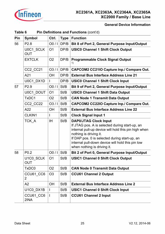
56 P2.8 O0 / I DP/B Bit 8 of Port 2, General Purpose Input/OutputU0C1_SCLKOUT
O1 DP/B USIC0 Channel 1 Shift Clock Output
EXTCLK O2 DP/B Programmable Clock Signal Output1)
CC2_CC21 O3 / I DP/B CAPCOM2 CC21IO Capture Inp./ Compare Out.A21 OH DP/B External Bus Interface Address Line 21U0C1_DX1D I DP/B USIC0 Channel 1 Shift Clock Input
57 P2.9 O0 / I St/B Bit 9 of Port 2, General Purpose Input/OutputU0C1_DOUT O1 St/B USIC0 Channel 1 Shift Data OutputTxDC1 O2 St/B CAN Node 1 Transmit Data OutputCC2_CC22 O3 / I St/B CAPCOM2 CC22IO Capture Inp./ Compare Out.A22 OH St/B External Bus Interface Address Line 22CLKIN1 I St/B Clock Signal Input 1TCK_A IH St/B DAP0/JTAG Clock Input
If JTAG pos. A is selected during start-up, an internal pull-up device will hold this pin high when nothing is driving it.If DAP pos. 0 is selected during start-up, an internal pull-down device will hold this pin low when nothing is driving it.
58 P0.2 O0 / I St/B Bit 2 of Port 0, General Purpose Input/OutputU1C0_SCLKOUT
O1 St/B USIC1 Channel 0 Shift Clock Output
TxDC0 O2 St/B CAN Node 0 Transmit Data OutputCCU61_CC62
O3 St/B CCU61 Channel 2 Output
A2 OH St/B External Bus Interface Address Line 2U1C0_DX1B I St/B USIC1 Channel 0 Shift Clock InputCCU61_CC62INA
I St/B CCU61 Channel 2 Input
Table 6 Pin Definitions and Functions (cont’d)
Pin Symbol Ctrl. Type Function
XC2361A, XC2363A, XC2364A, XC2365AXC2000 Family / Base Line
General Device Information
Data Sheet 26 V2.12, 2014-06
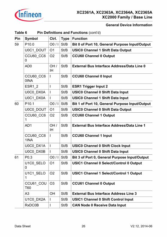
59 P10.0 O0 / I St/B Bit 0 of Port 10, General Purpose Input/OutputU0C1_DOUT O1 St/B USIC0 Channel 1 Shift Data OutputCCU60_CC60
O2 St/B CCU60 Channel 0 Output
AD0 OH / IH
St/B External Bus Interface Address/Data Line 0
CCU60_CC60INA
I St/B CCU60 Channel 0 Input
ESR1_2 I St/B ESR1 Trigger Input 2U0C0_DX0A I St/B USIC0 Channel 0 Shift Data InputU0C1_DX0A I St/B USIC0 Channel 1 Shift Data Input
60 P10.1 O0 / I St/B Bit 1 of Port 10, General Purpose Input/OutputU0C0_DOUT O1 St/B USIC0 Channel 0 Shift Data OutputCCU60_CC61
O2 St/B CCU60 Channel 1 Output
AD1 OH / IH
St/B External Bus Interface Address/Data Line 1
CCU60_CC61INA
I St/B CCU60 Channel 1 Input
U0C0_DX1A I St/B USIC0 Channel 0 Shift Clock InputU0C0_DX0B I St/B USIC0 Channel 0 Shift Data Input
61 P0.3 O0 / I St/B Bit 3 of Port 0, General Purpose Input/OutputU1C0_SELO0
O1 St/B USIC1 Channel 0 Select/Control 0 Output
U1C1_SELO1
O2 St/B USIC1 Channel 1 Select/Control 1 Output
CCU61_COUT60
O3 St/B CCU61 Channel 0 Output
A3 OH St/B External Bus Interface Address Line 3U1C0_DX2A I St/B USIC1 Channel 0 Shift Control InputRxDC0B I St/B CAN Node 0 Receive Data Input
Table 6 Pin Definitions and Functions (cont’d)
Pin Symbol Ctrl. Type Function

XC2361A, XC2363A, XC2364A, XC2365AXC2000 Family / Base Line
General Device Information
Data Sheet 27 V2.12, 2014-06
62 P10.2 O0 / I St/B Bit 2 of Port 10, General Purpose Input/OutputU0C0_SCLKOUT
O1 St/B USIC0 Channel 0 Shift Clock Output
CCU60_CC62
O2 St/B CCU60 Channel 2 Output
AD2 OH / IH
St/B External Bus Interface Address/Data Line 2
CCU60_CC62INA
I St/B CCU60 Channel 2 Input
U0C0_DX1B I St/B USIC0 Channel 0 Shift Clock Input63 P0.4 O0 / I St/B Bit 4 of Port 0, General Purpose Input/Output
U1C1_SELO0
O1 St/B USIC1 Channel 1 Select/Control 0 Output
U1C0_SELO1
O2 St/B USIC1 Channel 0 Select/Control 1 Output
CCU61_COUT61
O3 St/B CCU61 Channel 1 Output
A4 OH St/B External Bus Interface Address Line 4U1C1_DX2A I St/B USIC1 Channel 1 Shift Control InputRxDC1B I St/B CAN Node 1 Receive Data InputESR2_8 I St/B ESR2 Trigger Input 8
65 P2.13 O0 / I St/B Bit 13 of Port 2, General Purpose Input/OutputU2C1_SELO2
O1 St/B USIC2 Channel 1 Select/Control 2 Output
RxDC2D I St/B CAN Node 2 Receive Data Input66 P2.10 O0 / I St/B Bit 10 of Port 2, General Purpose Input/Output
U0C1_DOUT O1 St/B USIC0 Channel 1 Shift Data OutputU0C0_SELO3
O2 St/B USIC0 Channel 0 Select/Control 3 Output
CC2_CC23 O3 / I St/B CAPCOM2 CC23IO Capture Inp./ Compare Out.A23 OH St/B External Bus Interface Address Line 23U0C1_DX0E I St/B USIC0 Channel 1 Shift Data InputCAPINA I St/B GPT12E Register CAPREL Capture Input
Table 6 Pin Definitions and Functions (cont’d)
Pin Symbol Ctrl. Type Function
XC2361A, XC2363A, XC2364A, XC2365AXC2000 Family / Base Line
General Device Information
Data Sheet 28 V2.12, 2014-06
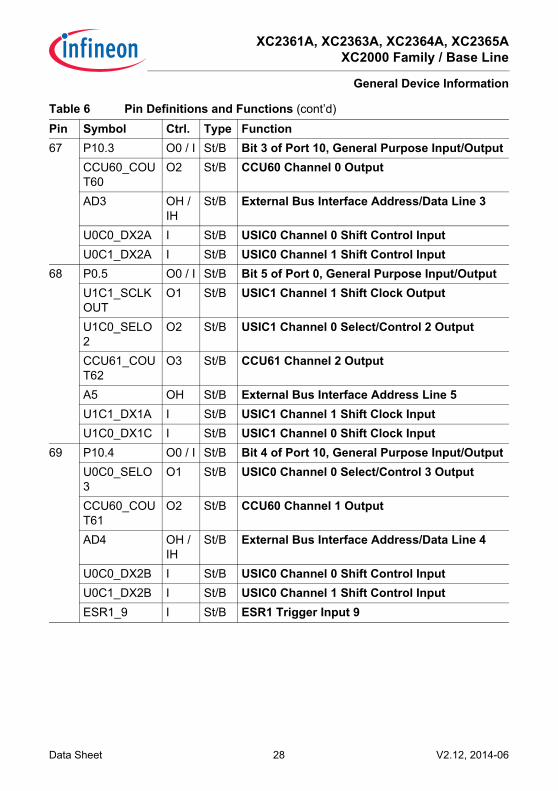
67 P10.3 O0 / I St/B Bit 3 of Port 10, General Purpose Input/OutputCCU60_COUT60
O2 St/B CCU60 Channel 0 Output
AD3 OH / IH
St/B External Bus Interface Address/Data Line 3
U0C0_DX2A I St/B USIC0 Channel 0 Shift Control InputU0C1_DX2A I St/B USIC0 Channel 1 Shift Control Input
68 P0.5 O0 / I St/B Bit 5 of Port 0, General Purpose Input/OutputU1C1_SCLKOUT
O1 St/B USIC1 Channel 1 Shift Clock Output
U1C0_SELO2
O2 St/B USIC1 Channel 0 Select/Control 2 Output
CCU61_COUT62
O3 St/B CCU61 Channel 2 Output
A5 OH St/B External Bus Interface Address Line 5U1C1_DX1A I St/B USIC1 Channel 1 Shift Clock InputU1C0_DX1C I St/B USIC1 Channel 0 Shift Clock Input
69 P10.4 O0 / I St/B Bit 4 of Port 10, General Purpose Input/OutputU0C0_SELO3
O1 St/B USIC0 Channel 0 Select/Control 3 Output
CCU60_COUT61
O2 St/B CCU60 Channel 1 Output
AD4 OH / IH
St/B External Bus Interface Address/Data Line 4
U0C0_DX2B I St/B USIC0 Channel 0 Shift Control InputU0C1_DX2B I St/B USIC0 Channel 1 Shift Control InputESR1_9 I St/B ESR1 Trigger Input 9
Table 6 Pin Definitions and Functions (cont’d)
Pin Symbol Ctrl. Type Function
XC2361A, XC2363A, XC2364A, XC2365AXC2000 Family / Base Line
General Device Information
Data Sheet 29 V2.12, 2014-06
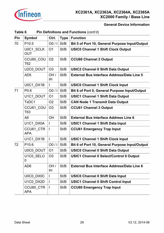
70 P10.5 O0 / I St/B Bit 5 of Port 10, General Purpose Input/OutputU0C1_SCLKOUT
O1 St/B USIC0 Channel 1 Shift Clock Output
CCU60_COUT62
O2 St/B CCU60 Channel 2 Output
U2C0_DOUT O3 St/B USIC2 Channel 0 Shift Data OutputAD5 OH /
IHSt/B External Bus Interface Address/Data Line 5
U0C1_DX1B I St/B USIC0 Channel 1 Shift Clock Input71 P0.6 O0 / I St/B Bit 6 of Port 0, General Purpose Input/Output
U1C1_DOUT O1 St/B USIC1 Channel 1 Shift Data OutputTxDC1 O2 St/B CAN Node 1 Transmit Data OutputCCU61_COUT63
O3 St/B CCU61 Channel 3 Output
A6 OH St/B External Bus Interface Address Line 6U1C1_DX0A I St/B USIC1 Channel 1 Shift Data InputCCU61_CTRAPA
I St/B CCU61 Emergency Trap Input
U1C1_DX1B I St/B USIC1 Channel 1 Shift Clock Input72 P10.6 O0 / I St/B Bit 6 of Port 10, General Purpose Input/Output
U0C0_DOUT O1 St/B USIC0 Channel 0 Shift Data OutputU1C0_SELO0
O3 St/B USIC1 Channel 0 Select/Control 0 Output
AD6 OH / IH
St/B External Bus Interface Address/Data Line 6
U0C0_DX0C I St/B USIC0 Channel 0 Shift Data InputU1C0_DX2D I St/B USIC1 Channel 0 Shift Control InputCCU60_CTRAPA
I St/B CCU60 Emergency Trap Input
Table 6 Pin Definitions and Functions (cont’d)
Pin Symbol Ctrl. Type Function

XC2361A, XC2363A, XC2364A, XC2365AXC2000 Family / Base Line
General Device Information
Data Sheet 30 V2.12, 2014-06
73 P10.7 O0 / I St/B Bit 7 of Port 10, General Purpose Input/OutputU0C1_DOUT O1 St/B USIC0 Channel 1 Shift Data OutputCCU60_COUT63
O2 St/B CCU60 Channel 3 Output
AD7 OH / IH
St/B External Bus Interface Address/Data Line 7
U0C1_DX0B I St/B USIC0 Channel 1 Shift Data InputCCU60_CCPOS0A
I St/B CCU60 Position Input 0
T4INB I St/B GPT12E Timer T4 Count/Gate Input74 P0.7 O0 / I St/B Bit 7 of Port 0, General Purpose Input/Output
U1C1_DOUT O1 St/B USIC1 Channel 1 Shift Data OutputU1C0_SELO3
O2 St/B USIC1 Channel 0 Select/Control 3 Output
A7 OH St/B External Bus Interface Address Line 7U1C1_DX0B I St/B USIC1 Channel 1 Shift Data InputCCU61_CTRAPB
I St/B CCU61 Emergency Trap Input
78 P1.0 O0 / I St/B Bit 0 of Port 1, General Purpose Input/OutputU1C0_MCLKOUT
O1 St/B USIC1 Channel 0 Master Clock Output
U1C0_SELO4
O2 St/B USIC1 Channel 0 Select/Control 4 Output
A8 OH St/B External Bus Interface Address Line 8ESR1_3 I St/B ESR1 Trigger Input 3T6INB I St/B GPT12E Timer T6 Count/Gate Input
Table 6 Pin Definitions and Functions (cont’d)
Pin Symbol Ctrl. Type Function

XC2361A, XC2363A, XC2364A, XC2365AXC2000 Family / Base Line
General Device Information
Data Sheet 31 V2.12, 2014-06
79 P10.8 O0 / I St/B Bit 8 of Port 10, General Purpose Input/OutputU0C0_MCLKOUT
O1 St/B USIC0 Channel 0 Master Clock Output
U0C1_SELO0
O2 St/B USIC0 Channel 1 Select/Control 0 Output
U2C1_DOUT O3 St/B USIC2 Channel 1 Shift Data OutputAD8 OH /
IHSt/B External Bus Interface Address/Data Line 8
CCU60_CCPOS1A
I St/B CCU60 Position Input 1
U0C0_DX1C I St/B USIC0 Channel 0 Shift Clock InputBRKIN_B I St/B OCDS Break Signal InputT3EUDB I St/B GPT12E Timer T3 External Up/Down Control
Input80 P10.9 O0 / I St/B Bit 9 of Port 10, General Purpose Input/Output
U0C0_SELO4
O1 St/B USIC0 Channel 0 Select/Control 4 Output
U0C1_MCLKOUT
O2 St/B USIC0 Channel 1 Master Clock Output
AD9 OH / IH
St/B External Bus Interface Address/Data Line 9
CCU60_CCPOS2A
I St/B CCU60 Position Input 2
TCK_B IH St/B DAP0/JTAG Clock InputIf JTAG pos. B is selected during start-up, an internal pull-up device will hold this pin high when nothing is driving it.If DAP pos. 1 is selected during start-up, an internal pull-down device will hold this pin low when nothing is driving it.
T3INB I St/B GPT12E Timer T3 Count/Gate Input
Table 6 Pin Definitions and Functions (cont’d)
Pin Symbol Ctrl. Type Function
XC2361A, XC2363A, XC2364A, XC2365AXC2000 Family / Base Line
General Device Information
Data Sheet 32 V2.12, 2014-06
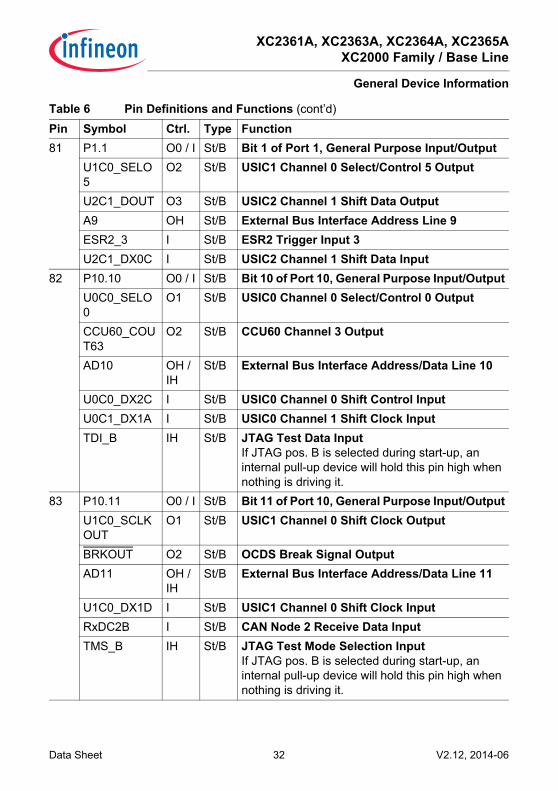
81 P1.1 O0 / I St/B Bit 1 of Port 1, General Purpose Input/OutputU1C0_SELO5
O2 St/B USIC1 Channel 0 Select/Control 5 Output
U2C1_DOUT O3 St/B USIC2 Channel 1 Shift Data OutputA9 OH St/B External Bus Interface Address Line 9ESR2_3 I St/B ESR2 Trigger Input 3U2C1_DX0C I St/B USIC2 Channel 1 Shift Data Input
82 P10.10 O0 / I St/B Bit 10 of Port 10, General Purpose Input/OutputU0C0_SELO0
O1 St/B USIC0 Channel 0 Select/Control 0 Output
CCU60_COUT63
O2 St/B CCU60 Channel 3 Output
AD10 OH / IH
St/B External Bus Interface Address/Data Line 10
U0C0_DX2C I St/B USIC0 Channel 0 Shift Control InputU0C1_DX1A I St/B USIC0 Channel 1 Shift Clock InputTDI_B IH St/B JTAG Test Data Input
If JTAG pos. B is selected during start-up, an internal pull-up device will hold this pin high when nothing is driving it.
83 P10.11 O0 / I St/B Bit 11 of Port 10, General Purpose Input/OutputU1C0_SCLKOUT
O1 St/B USIC1 Channel 0 Shift Clock Output
BRKOUT O2 St/B OCDS Break Signal OutputAD11 OH /
IHSt/B External Bus Interface Address/Data Line 11
U1C0_DX1D I St/B USIC1 Channel 0 Shift Clock InputRxDC2B I St/B CAN Node 2 Receive Data InputTMS_B IH St/B JTAG Test Mode Selection Input
If JTAG pos. B is selected during start-up, an internal pull-up device will hold this pin high when nothing is driving it.
Table 6 Pin Definitions and Functions (cont’d)
Pin Symbol Ctrl. Type Function

XC2361A, XC2363A, XC2364A, XC2365AXC2000 Family / Base Line
General Device Information
Data Sheet 33 V2.12, 2014-06
84 P1.2 O0 / I St/B Bit 2 of Port 1, General Purpose Input/OutputU1C0_SELO6
O2 St/B USIC1 Channel 0 Select/Control 6 Output
U2C1_SCLKOUT
O3 St/B USIC2 Channel 1 Shift Clock Output
A10 OH St/B External Bus Interface Address Line 10ESR1_4 I St/B ESR1 Trigger Input 4CCU61_T12HRB
I St/B External Run Control Input for T12 of CCU61
U2C1_DX0D I St/B USIC2 Channel 1 Shift Data InputU2C1_DX1C I St/B USIC2 Channel 1 Shift Clock Input
85 P10.12 O0 / I St/B Bit 12 of Port 10, General Purpose Input/OutputU1C0_DOUT O1 St/B USIC1 Channel 0 Shift Data OutputTxDC2 O2 St/B CAN Node 2 Transmit Data OutputTDO_B OH /
IHSt/B JTAG Test Data Output / DAP1 Input/Output
If DAP pos. 1 is selected during start-up, an internal pull-down device will hold this pin low when nothing is driving it.
AD12 OH / IH
St/B External Bus Interface Address/Data Line 12
U1C0_DX0C I St/B USIC1 Channel 0 Shift Data InputU1C0_DX1E I St/B USIC1 Channel 0 Shift Clock Input
86 P10.13 O0 / I St/B Bit 13 of Port 10, General Purpose Input/OutputU1C0_DOUT O1 St/B USIC1 Channel 0 Shift Data OutputU1C0_SELO3
O3 St/B USIC1 Channel 0 Select/Control 3 Output
WR/WRL OH St/B External Bus Interface Write Strobe OutputActive for each external write access, when WR,active for ext. writes to the low byte, when WRL.
U1C0_DX0D I St/B USIC1 Channel 0 Shift Data Input
Table 6 Pin Definitions and Functions (cont’d)
Pin Symbol Ctrl. Type Function

XC2361A, XC2363A, XC2364A, XC2365AXC2000 Family / Base Line
General Device Information
Data Sheet 34 V2.12, 2014-06
87 P1.3 O0 / I St/B Bit 3 of Port 1, General Purpose Input/OutputU1C0_SELO7
O2 St/B USIC1 Channel 0 Select/Control 7 Output
U2C0_SELO4
O3 St/B USIC2 Channel 0 Select/Control 4 Output
A11 OH St/B External Bus Interface Address Line 11ESR2_4 I St/B ESR2 Trigger Input 4
89 P10.14 O0 / I St/B Bit 14 of Port 10, General Purpose Input/OutputU1C0_SELO1
O1 St/B USIC1 Channel 0 Select/Control 1 Output
U0C1_DOUT O2 St/B USIC0 Channel 1 Shift Data OutputRD OH St/B External Bus Interface Read Strobe OutputESR2_2 I St/B ESR2 Trigger Input 2U0C1_DX0C I St/B USIC0 Channel 1 Shift Data Input
90 P1.4 O0 / I St/B Bit 4 of Port 1, General Purpose Input/OutputU1C1_SELO4
O2 St/B USIC1 Channel 1 Select/Control 4 Output
U2C0_SELO5
O3 St/B USIC2 Channel 0 Select/Control 5 Output
A12 OH St/B External Bus Interface Address Line 12U2C0_DX2B I St/B USIC2 Channel 0 Shift Control Input
91 P10.15 O0 / I St/B Bit 15 of Port 10, General Purpose Input/OutputU1C0_SELO2
O1 St/B USIC1 Channel 0 Select/Control 2 Output
U0C1_DOUT O2 St/B USIC0 Channel 1 Shift Data OutputU1C0_DOUT O3 St/B USIC1 Channel 0 Shift Data OutputALE OH St/B External Bus Interf. Addr. Latch Enable OutputU0C1_DX1C I St/B USIC0 Channel 1 Shift Clock Input
Table 6 Pin Definitions and Functions (cont’d)
Pin Symbol Ctrl. Type Function

XC2361A, XC2363A, XC2364A, XC2365AXC2000 Family / Base Line
General Device Information
Data Sheet 35 V2.12, 2014-06
92 P1.5 O0 / I St/B Bit 5 of Port 1, General Purpose Input/OutputU1C1_SELO3
O2 St/B USIC1 Channel 1 Select/Control 3 Output
BRKOUT O3 St/B OCDS Break Signal OutputA13 OH St/B External Bus Interface Address Line 13U2C0_DX0C I St/B USIC2 Channel 0 Shift Data Input
93 P1.6 O0 / I St/B Bit 6 of Port 1, General Purpose Input/OutputU1C1_SELO2
O2 St/B USIC1 Channel 1 Select/Control 2 Output
U2C0_DOUT O3 St/B USIC2 Channel 0 Shift Data OutputA14 OH St/B External Bus Interface Address Line 14U2C0_DX0D I St/B USIC2 Channel 0 Shift Data Input
94 P1.7 O0 / I St/B Bit 7 of Port 1, General Purpose Input/OutputU1C1_MCLKOUT
O2 St/B USIC1 Channel 1 Master Clock Output
U2C0_SCLKOUT
O3 St/B USIC2 Channel 0 Shift Clock Output
A15 OH St/B External Bus Interface Address Line 15U2C0_DX1C I St/B USIC2 Channel 0 Shift Clock Input
95 XTAL2 O Sp/M Crystal Oscillator Amplifier Output96 XTAL1 I Sp/M Crystal Oscillator Amplifier Input
To clock the device from an external source, drive XTAL1, while leaving XTAL2 unconnected.Voltages on XTAL1 must comply to the core supply voltage VDDIM.
ESR2_9 I St/B ESR2 Trigger Input 997 PORST I In/B Power On Reset Input
A low level at this pin resets the XC236xA completely. A spike filter suppresses input pulses <10 ns. Input pulses >100 ns safely pass the filter. The minimum duration for a safe recognition should be 120 ns.An internal pull-up device will hold this pin high when nothing is driving it.
Table 6 Pin Definitions and Functions (cont’d)
Pin Symbol Ctrl. Type Function

XC2361A, XC2363A, XC2364A, XC2365AXC2000 Family / Base Line
General Device Information
Data Sheet 36 V2.12, 2014-06
98 ESR1 O0 / I St/B External Service Request 1After power-up, an internal weak pull-up device holds this pin high when nothing is driving it.
RxDC0E I St/B CAN Node 0 Receive Data InputU1C0_DX0F I St/B USIC1 Channel 0 Shift Data InputU1C0_DX2C I St/B USIC1 Channel 0 Shift Control InputU1C1_DX0C I St/B USIC1 Channel 1 Shift Data InputU1C1_DX2B I St/B USIC1 Channel 1 Shift Control InputU2C1_DX2C I St/B USIC2 Channel 1 Shift Control Input
99 ESR0 O0 / I St/B External Service Request 0After power-up, ESR0 operates as open-drain bidirectional reset with a weak pull-up.
U1C0_DX0E I St/B USIC1 Channel 0 Shift Data InputU1C0_DX2B I St/B USIC1 Channel 0 Shift Control Input
10 VDDIM - PS/M Digital Core Supply Voltage for Domain MDecouple with a ceramic capacitor, see Data Sheet for details.
38, 64, 88
VDDI1 - PS/1 Digital Core Supply Voltage for Domain 1Decouple with a ceramic capacitor, see Data Sheet for details.All VDDI1 pins must be connected to each other.
14 VDDPA - PS/A Digital Pad Supply Voltage for Domain AConnect decoupling capacitors to adjacent VDDP/VSS pin pairs as close as possible to the pins.Note: The A/D_Converters and ports P5, P6 and
P15 are fed from supply voltage VDDPA.
Table 6 Pin Definitions and Functions (cont’d)
Pin Symbol Ctrl. Type Function
XC2361A, XC2363A, XC2364A, XC2365AXC2000 Family / Base Line
General Device Information
Data Sheet 37 V2.12, 2014-06
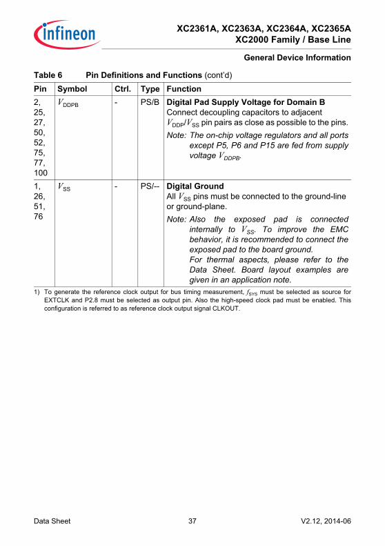
2, 25, 27, 50, 52, 75, 77, 100
VDDPB - PS/B Digital Pad Supply Voltage for Domain BConnect decoupling capacitors to adjacent VDDP/VSS pin pairs as close as possible to the pins.Note: The on-chip voltage regulators and all ports
except P5, P6 and P15 are fed from supplyvoltage VDDPB.
1, 26, 51, 76
VSS - PS/-- Digital GroundAll VSS pins must be connected to the ground-line or ground-plane.Note: Also the exposed pad is connected
internally to VSS. To improve the EMCbehavior, it is recommended to connect theexposed pad to the board ground.For thermal aspects, please refer to theData Sheet. Board layout examples aregiven in an application note.
1) To generate the reference clock output for bus timing measurement, fSYS must be selected as source forEXTCLK and P2.8 must be selected as output pin. Also the high-speed clock pad must be enabled. Thisconfiguration is referred to as reference clock output signal CLKOUT.
Table 6 Pin Definitions and Functions (cont’d)
Pin Symbol Ctrl. Type Function
XC2361A, XC2363A, XC2364A, XC2365AXC2000 Family / Base Line
General Device Information
Data Sheet 38 V2.12, 2014-06
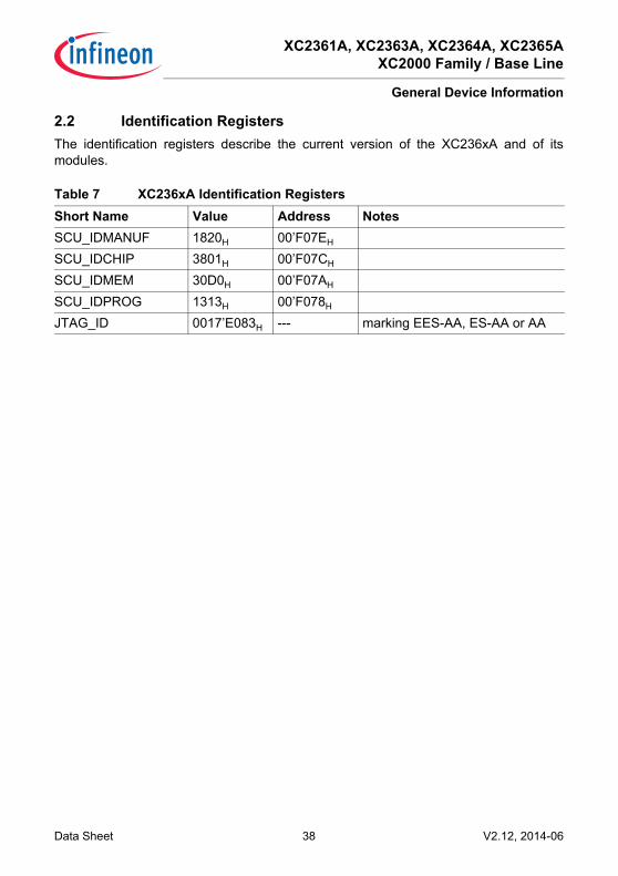
2.2 Identification RegistersThe identification registers describe the current version of the XC236xA and of itsmodules.
Table 7 XC236xA Identification RegistersShort Name Value Address NotesSCU_IDMANUF 1820H 00’F07EH
SCU_IDCHIP 3801H 00’F07CH
SCU_IDMEM 30D0H 00’F07AH
SCU_IDPROG 1313H 00’F078H
JTAG_ID 0017’E083H --- marking EES-AA, ES-AA or AA
XC2361A, XC2363A, XC2364A, XC2365AXC2000 Family / Base Line
Functional Description
Data Sheet 39 V2.12, 2014-06
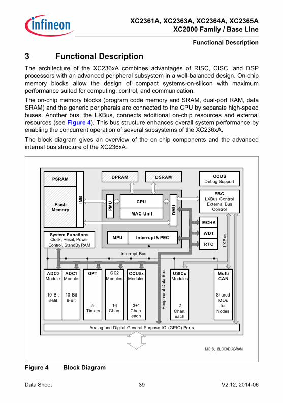
3 Functional DescriptionThe architecture of the XC236xA combines advantages of RISC, CISC, and DSPprocessors with an advanced peripheral subsystem in a well-balanced design. On-chipmemory blocks allow the design of compact systems-on-silicon with maximumperformance suited for computing, control, and communication.The on-chip memory blocks (program code memory and SRAM, dual-port RAM, dataSRAM) and the generic peripherals are connected to the CPU by separate high-speedbuses. Another bus, the LXBus, connects additional on-chip resources and externalresources (see Figure 4). This bus structure enhances overall system performance byenabling the concurrent operation of several subsystems of the XC236xA.The block diagram gives an overview of the on-chip components and the advancedinternal bus structure of the XC236xA.
Figure 4 Block Diagram
DPRAM
CPU
PMU
DM
U
ADC0Module
10-Bit8-Bit
RTC
MCHK
Interrupt & PEC
EBCLXBus ControlExternal Bus
Control
DSRAM
System FunctionsClock, Reset, Power
Control, StandBy RAM
OCDSDebug Support
Interrupt Bus
Per
iph
eral
Dat
a B
us
Analog and Digital General Purpose IO (GPIO) Ports
MC_BL_BLOCKDIAGRAM
GPT
5Timers
CC2Modules
16Chan.
LXB
us
WDT
MultiCAN
SharedMOsfor
Nodes
CCU6xModules
3+1Chan.each
USICxModules
2 Chan.each
PSRAM
FlashMemory
IMB
MAC Unit
MPU
ADC1Module
10-Bit8-Bit

XC2361A, XC2363A, XC2364A, XC2365AXC2000 Family / Base Line
Functional Description
Data Sheet 40 V2.12, 2014-06
3.1 Memory Subsystem and OrganizationThe memory space of the XC236xA is configured in the von Neumann architecture. Inthis architecture all internal and external resources, including code memory, datamemory, registers and I/O ports, are organized in the same linear address space.
Table 8 XC236xA Memory Map 1)
Address Area Start Loc. End Loc. Area Size2) NotesIMB register space FF’FF00H FF’FFFFH 256 Bytes –Reserved (Access trap) F0’0000H FF’FEFFH <1 Mbyte Minus IMB registersReserved for EPSRAM E8’8000H EF’FFFFH 480 Kbytes Mirrors EPSRAMEmulated PSRAM E8’0000H E8’7FFFH 32 Kbytes With Flash timingReserved for PSRAM E0’8000H E7’FFFFH 480 Kbytes Mirrors PSRAMProgram SRAM E0’0000H E0’7FFFH 32 Kbytes Maximum speedReserved for Flash CD’0000H DF’FFFFH <1.25 Mbytes –Program Flash 3 CC’0000H CC’FFFFH 64 Kbytes –Program Flash 2 C8’0000H CB’FFFFH 256 Kbytes –Program Flash 1 C4’0000H C7’FFFFH 256 Kbytes –Program Flash 0 C0’0000H C3’FFFFH 256 Kbytes 3)
External memory area 40’0000H BF’FFFFH 8 Mbytes –Available Ext. IO area4) 21’0000H 3F’FFFFH < 2 Mbytes Minus USIC/CANReserved 20’BC00H 20’FFFFH 17 Kbytes –USIC alternate regs. 20’B000H 20’BFFFH 4 Kbytes Accessed via EBCMultiCAN alternate regs.
20’8000H 20’AFFFH 12 Kbytes Accessed via EBC
Reserved 20’6000H 20’7FFFH 8 Kbytes –USIC registers 20’4000H 20’5FFFH 8 Kbytes Accessed via EBCMultiCAN registers 20’0000H 20’3FFFH 16 Kbytes Accessed via EBCExternal memory area 01’0000H 1F’FFFFH < 2 Mbytes Minus segment 0SFR area 00’FE00H 00’FFFFH 0.5 Kbyte –Dual-Port RAM 00’F600H 00’FDFFH 2 Kbytes –Reserved for DPRAM 00’F200H 00’F5FFH 1 Kbyte –ESFR area 00’F000H 00’F1FFH 0.5 Kbyte –XSFR area 00’E000H 00’EFFFH 4 Kbytes –

XC2361A, XC2363A, XC2364A, XC2365AXC2000 Family / Base Line
Functional Description
Data Sheet 41 V2.12, 2014-06
This common memory space consists of 16 Mbytes organized as 256 segments of64 Kbytes; each segment contains four data pages of 16 Kbytes. The entire memoryspace can be accessed bytewise or wordwise. Portions of the on-chip DPRAM and theregister spaces (ESFR/SFR) additionally are directly bit addressable.The internal data memory areas and the Special Function Register areas (SFR andESFR) are mapped into segment 0, the system segment.The Program Management Unit (PMU) handles all code fetches and, therefore, controlsaccess to the program memories such as Flash memory and PSRAM.The Data Management Unit (DMU) handles all data transfers and, therefore, controlsaccess to the DSRAM and the on-chip peripherals.Both units (PMU and DMU) are connected to the high-speed system bus so that they canexchange data. This is required if operands are read from program memory, code ordata is written to the PSRAM, code is fetched from external memory, or data is read fromor written to external resources. These include peripherals on the LXBus such as USICor MultiCAN. The system bus allows concurrent two-way communication for maximumtransfer performance.Up to 32 Kbytes of on-chip Program SRAM (PSRAM) are provided to store user codeor data. The PSRAM is accessed via the PMU and is optimized for code fetches. Asection of the PSRAM with programmable size can be write-protected.Up to 16 Kbytes of on-chip Data SRAM (DSRAM) are used for storage of general userdata. The DSRAM is accessed via a separate interface and is optimized for data access.2 Kbytes of on-chip Dual-Port RAM (DPRAM) provide storage for user-definedvariables, for the system stack, and for general purpose register banks. A register bankcan consist of up to 16 word-wide (R0 to R15) and/or byte-wide (RL0, RH0, …, RL7,RH7) General Purpose Registers (GPRs).The upper 256 bytes of the DPRAM are directly bit addressable. When used by a GPR,any location in the DPRAM is bit addressable.
Data SRAM 00’A000H 00’DFFFH 16 Kbytes –Reserved for DSRAM 00’8000H 00’9FFFH 8 Kbytes –External memory area 00’0000H 00’7FFFH 32 Kbytes –1) Accesses to the shaded areas are reserved. In devices with external bus interface these accesses generate
external bus accesses.2) The areas marked with “<” are slightly smaller than indicated. See column “Notes”.3) The uppermost 4-Kbyte sector of the first Flash segment is reserved for internal use (C0’F000H to C0’FFFFH).4) Several pipeline optimizations are not active within the external IO area. This is necessary to control external
peripherals properly.
Table 8 XC236xA Memory Map (cont’d)1)
Address Area Start Loc. End Loc. Area Size2) Notes
XC2361A, XC2363A, XC2364A, XC2365AXC2000 Family / Base Line
Functional Description
Data Sheet 42 V2.12, 2014-06
8 Kbytes of on-chip Stand-By SRAM (SBRAM) provide storage for system-relevantuser data that must be preserved while the major part of the device is powered down.The SBRAM is accessed via a specific interface and is powered in domain M.1024 bytes (2 × 512 bytes) of the address space are reserved for the Special FunctionRegister areas (SFR space and ESFR space). SFRs are word-wide registers which areused to control and monitor functions of the different on-chip units. Unused SFRaddresses are reserved for future members of the XC2000 Family. In order to ensureupward compatibility they should either not be accessed or written with zeros.The on-chip Flash memory stores code, constant data, and control data. The on-chipFlash memory consists of 1 module of 64 Kbytes (preferably for data storage) andmodules with a maximum capacity of 256 Kbytes each. Each module is organized insectors of 4 Kbytes.The uppermost 4-Kbyte sector of segment 0 (located in Flash module 0) is usedinternally to store operation control parameters and protection information.Note: The actual size of the Flash memory depends on the chosen device type.
Each sector can be separately write protected1), erased and programmed (in blocks of128 Bytes). The complete Flash area can be read-protected. A user-defined passwordsequence temporarily unlocks protected areas. The Flash modules combine 128-bitread access with protected and efficient writing algorithms for programming and erasing.Dynamic error correction provides extremely high read data security for all read accessoperations. Access to different Flash modules can be executed in parallel.For Flash parameters, please see Section 4.5.
Memory Content ProtectionThe contents of on-chip memories can be protected against soft errors (induced e.g. byradiation) by activating the parity mechanism or the Error Correction Code (ECC).The parity mechanism can detect a single-bit error and prevent the software from usingincorrect data or executing incorrect instructions.The ECC mechanism can detect and automatically correct single-bit errors. Thissupports the stable operation of the system.It is strongly recommended to activate the ECC mechanism wherever possible becausethis dramatically increases the robustness of an application against such soft errors.
1) To save control bits, sectors are clustered for protection purposes, they remain separate forprogramming/erasing.

XC2361A, XC2363A, XC2364A, XC2365AXC2000 Family / Base Line
Functional Description
Data Sheet 43 V2.12, 2014-06
3.2 External Bus ControllerAll external memory access operations are performed by a special on-chip External BusController (EBC). The EBC also controls access to resources connected to the on-chipLXBus (MultiCAN and the USIC modules). The LXBus is an internal representation ofthe external bus that allows access to integrated peripherals and modules in the sameway as to external components.The EBC can be programmed either to Single Chip Mode, when no external memory isrequired, or to an external bus mode with the following selections1):• Address Bus Width with a range of 0 … 24-bit• Data Bus Width 8-bit or 16-bit• Bus Operation Multiplexed or DemultiplexedThe bus interface uses Port 10 and Port 2 for addresses and data. In the demultiplexedbus modes, the lower addresses are output separately on Port 0 and Port 1. The numberof active segment address lines is selectable, restricting the external address space to8 Mbytes … 64 Kbytes. This is required when interface lines shall be assigned to Port 2.External CS signals (address windows plus default) can be generated and output onPort 4 in order to save external glue logic. External modules can be directly connectedto the common address/data bus and their individual select lines.Important timing characteristics of the external bus interface are programmable (withregisters TCONCSx/FCONCSx) to allow the user to adapt it to a wide range of differenttypes of memories and external peripherals.Access to very slow memories or modules with varying access times is supported by aspecial ‘Ready’ function. The active level of the control input signal is selectable.In addition, up to four independent address windows may be defined (using registersADDRSELx) to control access to resources with different bus characteristics. Theseaddress windows are arranged hierarchically where window 4 overrides window 3, andwindow 2 overrides window 1. All accesses to locations not covered by these fouraddress windows are controlled by TCONCS0/FCONCS0. The currently active windowcan generate a chip select signal.The external bus timing is based on the rising edge of the reference clock outputCLKOUT. The external bus protocol is compatible with that of the standard C166 Family.
1) Bus modes are switched dynamically if several address windows with different mode settings are used.

XC2361A, XC2363A, XC2364A, XC2365AXC2000 Family / Base Line
Functional Description
Data Sheet 44 V2.12, 2014-06
3.3 Central Processing Unit (CPU)The core of the CPU consists of a 5-stage execution pipeline with a 2-stage instruction-fetch pipeline, a 16-bit arithmetic and logic unit (ALU), a 32-bit/40-bit multiply andaccumulate unit (MAC), a register-file providing three register banks, and dedicatedSFRs. The ALU features a multiply-and-divide unit, a bit-mask generator, and a barrelshifter.
Figure 5 CPU Block Diagram
DPRAM
CPU
IPIP
RFR0R1
GPRs
R14R15
R0R1
GPRs
R14R15
IFU
Injection/ExceptionHandler
ADU
MAC
mca04917_x.vsd
CPUCON1CPUCON2
CSP IP
ReturnStackFIFO
BranchUnit
PrefetchUnit
VECSEG
TFR
+/-
IDX0IDX1QX0QX1
QR0QR1
DPP0DPP1DPP2DPP3
SPSEGSP
STKOVSTKUN
+/-
MRW
MCWMSW
MAL
+/-
MAH
MultiplyUnit
ALU
Division Unit
Multiply Unit
Bit-Mask-Gen.
Barrel-Shifter
+/-MDC
PSW
MDH
ZEROS
MDL
ONES
R0R1
GPRs
R14R15
CP
WB
Buffer
2-StagePrefetch
Pipeline
5-StagePipeline
R0R1
GPRs
R14R15
PMU
DMU
DSRAMEBC
Peripherals
PSRAMFlash/ROM

XC2361A, XC2363A, XC2364A, XC2365AXC2000 Family / Base Line
Functional Description
Data Sheet 45 V2.12, 2014-06
With this hardware most XC236xA instructions are executed in a single machine cycleof 12.5 ns with an 80-MHz CPU clock. For example, shift and rotate instructions arealways processed during one machine cycle, no matter how many bits are shifted. Also,multiplication and most MAC instructions execute in one cycle. All multiple-cycleinstructions have been optimized so that they can be executed very fast; for example, a32-/16-bit division is started within 4 cycles while the remaining cycles are executed inthe background. Another pipeline optimization, the branch target prediction, eliminatesthe execution time of branch instructions if the prediction was correct.The CPU has a register context consisting of up to three register banks with 16 word-wide GPRs each at its disposal. One of these register banks is physically allocated withinthe on-chip DPRAM area. A Context Pointer (CP) register determines the base addressof the active register bank accessed by the CPU at any time. The number of theseregister bank copies is only restricted by the available internal RAM space. For easyparameter passing, a register bank may overlap others.A system stack of up to 32 Kwords is provided for storage of temporary data. The systemstack can be allocated to any location within the address space (preferably in the on-chipRAM area); it is accessed by the CPU with the stack pointer (SP) register. Two separateSFRs, STKOV and STKUN, are implicitly compared with the stack pointer value duringeach stack access to detect stack overflow or underflow.The high performance of the CPU hardware implementation can be best utilized by theprogrammer with the highly efficient XC236xA instruction set. This includes the followinginstruction classes:• Standard Arithmetic Instructions• DSP-Oriented Arithmetic Instructions• Logical Instructions• Boolean Bit Manipulation Instructions• Compare and Loop Control Instructions• Shift and Rotate Instructions• Prioritize Instruction• Data Movement Instructions• System Stack Instructions• Jump and Call Instructions• Return Instructions• System Control Instructions• Miscellaneous InstructionsThe basic instruction length is either 2 or 4 bytes. Possible operand types are bits, bytesand words. A variety of direct, indirect or immediate addressing modes are provided tospecify the required operands.

XC2361A, XC2363A, XC2364A, XC2365AXC2000 Family / Base Line
Functional Description
Data Sheet 46 V2.12, 2014-06
3.4 Memory Protection Unit (MPU)The XC236xA’s Memory Protection Unit (MPU) protects user-specified memory areasfrom unauthorized read, write, or instruction fetch accesses. The MPU can protect thewhole address space including the peripheral area. This completes establischedmechanisms such as the register security mechanism or stack overrun/underrundetection.Four Protection Levels support flexible system programming where operating system,low level drivers, and applications run on separate levels. Each protection level permitsdifferent access restrictions for instructions and/or data.Every access is checked (if the MPU is enabled) and an access violating the permissionrules will be marked as invalid and leads to a protection trap.A set of protection registers for each protection level specifies the address ranges andthe access permissions. Applications requiring more than 4 protection levels candynamically re-program the protection registers.
3.5 Memory Checker Module (MCHK)The XC236xA’s Memory Checker Module calculates a checksum (fractional polynomialdivision) on a block of data, often called Cyclic Redundancy Code (CRC). It is based ona 32-bit linear feedback shift register and may, therefore, also be used to generatepseudo-random numbers.The Memory Checker Module is a 16-bit parallel input signature compression circuitrywhich enables error detection within a block of data stored in memory, registers, orcommunicated e.g. via serial communication lines. It reduces the probability of errormasking due to repeated error patterns by calculating the signature of blocks of data.The polynomial used for operation is configurable, so most of the commonly usedpolynomials may be used. Also, the block size for generating a CRC result isconfigurable via a local counter. An interrupt may be generated if testing the current datablock reveals an error.An autonomous CRC compare circuitry is included to enable redundant error detection,e.g. to enable higher safety integrity levels.The Memory Checker Module provides enhanced fault detection (beyond parity or ECC)for data and instructions in volatile and non volatile memories. This is especiallyimportant for the safety and reliability of embedded systems.

XC2361A, XC2363A, XC2364A, XC2365AXC2000 Family / Base Line
Functional Description
Data Sheet 47 V2.12, 2014-06
3.6 Interrupt SystemThe architecture of the XC236xA supports several mechanisms for fast and flexibleresponse to service requests; these can be generated from various sources internal orexternal to the microcontroller. Any of these interrupt requests can be programmed to beserviced by the Interrupt Controller or by the Peripheral Event Controller (PEC).Where in a standard interrupt service the current program execution is suspended anda branch to the interrupt vector table is performed, just one cycle is ‘stolen’ from thecurrent CPU activity to perform a PEC service. A PEC service implies a single byte orword data transfer between any two memory locations with an additional increment ofeither the PEC source pointer, the destination pointer, or both. An individual PECtransfer counter is implicitly decremented for each PEC service except when performingin the continuous transfer mode. When this counter reaches zero, a standard interrupt isperformed to the corresponding source-related vector location. PEC services areparticularly well suited to supporting the transmission or reception of blocks of data. TheXC236xA has eight PEC channels, each whith fast interrupt-driven data transfercapabilities.With a minimum interrupt response time of 7/111) CPU clocks, the XC236xA can reactquickly to the occurrence of non-deterministic events.
Interrupt Nodes and Source SelectionThe interrupt system provides 96 physical nodes with separate control registercontaining an interrupt request flag, an interrupt enable flag and an interrupt priority bitfield. Most interrupt sources are assigned to a dedicated node. A particular subset ofinterrupt sources shares a set of nodes. The source selection can be programmed usingthe interrupt source selection (ISSR) registers.
External Request Unit (ERU)A dedicated External Request Unit (ERU) is provided to route and preprocess selectedon-chip peripheral and external interrupt requests. The ERU features 4 programmableinput channels with event trigger logic (ETL) a routing matrix and 4 output gating units(OGU). The ETL features rising edge, falling edge, or both edges event detection. TheOGU combines the detected interrupt events and provides filtering capabilitiesdepending on a programmable pattern match or miss.
Trap ProcessingThe XC236xA provides efficient mechanisms to identify and process exceptions or errorconditions that arise during run-time, the so-called ‘Hardware Traps’. A hardware trapcauses an immediate system reaction similar to a standard interrupt service (branching
1) Depending if the jump cache is used or not.

XC2361A, XC2363A, XC2364A, XC2365AXC2000 Family / Base Line
Functional Description
Data Sheet 48 V2.12, 2014-06
to a dedicated vector table location). The occurrence of a hardware trap is also indicatedby a single bit in the trap flag register (TFR). Unless another higher-priority trap serviceis in progress, a hardware trap will interrupt any ongoing program execution. In turn,hardware trap services can normally not be interrupted by standard or PEC interrupts.Depending on the package option up to 3 External Service Request (ESR) pins areprovided. The ESR unit processes their input values and allows to implement usercontrolled trap functions (System Requests SR0 and SR1). In this way reset, wakeupand power control can be efficiently realized.Software interrupts are supported by the ‘TRAP’ instruction in combination with anindividual trap (interrupt) number. Alternatively to emulate an interrupt by software aprogram can trigger interrupt requests by writing the Interrupt Request (IR) bit of aninterrupt control register.
3.7 On-Chip Debug Support (OCDS)The On-Chip Debug Support system built into the XC236xA provides a broad range ofdebug and emulation features. User software running on the XC236xA can be debuggedwithin the target system environment.The OCDS is controlled by an external debugging device via the debug interface. Thiseither consists of the 2-pin Device Access Port (DAP) or of the JTAG port conforming toIEEE-1149. The debug interface can be completed with an optional break interface.The debugger controls the OCDS with a set of dedicated registers accessible via thedebug interface (DAP or JTAG). In addition the OCDS system can be controlled by theCPU, e.g. by a monitor program. An injection interface allows the execution of OCDS-generated instructions by the CPU.Multiple breakpoints can be triggered by on-chip hardware, by software, or by anexternal trigger input. Single stepping is supported, as is the injection of arbitraryinstructions and read/write access to the complete internal address space. A breakpointtrigger can be answered with a CPU halt, a monitor call, a data transfer, or/and theactivation of an external signal.Tracing data can be obtained via the debug interface, or via the external bus interfacefor increased performance.Tracing of program execution is supported by the XC2000 Family emulation device.The DAP interface uses two interface signals, the JTAG interface uses four interfacesignals, to communicate with external circuitry. The debug interface can be amendedwith two optional break lines.
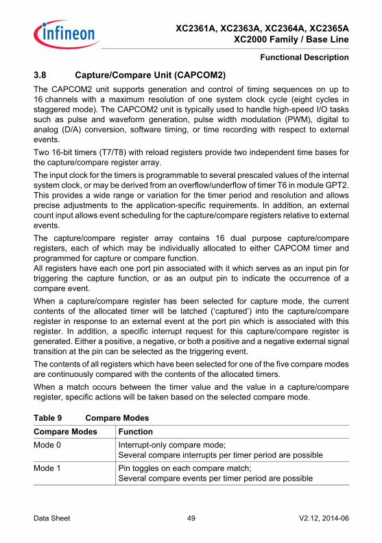
XC2361A, XC2363A, XC2364A, XC2365AXC2000 Family / Base Line
Functional Description
Data Sheet 49 V2.12, 2014-06
3.8 Capture/Compare Unit (CAPCOM2)The CAPCOM2 unit supports generation and control of timing sequences on up to16 channels with a maximum resolution of one system clock cycle (eight cycles instaggered mode). The CAPCOM2 unit is typically used to handle high-speed I/O taskssuch as pulse and waveform generation, pulse width modulation (PWM), digital toanalog (D/A) conversion, software timing, or time recording with respect to externalevents.Two 16-bit timers (T7/T8) with reload registers provide two independent time bases forthe capture/compare register array.The input clock for the timers is programmable to several prescaled values of the internalsystem clock, or may be derived from an overflow/underflow of timer T6 in module GPT2.This provides a wide range or variation for the timer period and resolution and allowsprecise adjustments to the application-specific requirements. In addition, an externalcount input allows event scheduling for the capture/compare registers relative to externalevents.The capture/compare register array contains 16 dual purpose capture/compareregisters, each of which may be individually allocated to either CAPCOM timer andprogrammed for capture or compare function.All registers have each one port pin associated with it which serves as an input pin fortriggering the capture function, or as an output pin to indicate the occurrence of acompare event.When a capture/compare register has been selected for capture mode, the currentcontents of the allocated timer will be latched (‘captured’) into the capture/compareregister in response to an external event at the port pin which is associated with thisregister. In addition, a specific interrupt request for this capture/compare register isgenerated. Either a positive, a negative, or both a positive and a negative external signaltransition at the pin can be selected as the triggering event.The contents of all registers which have been selected for one of the five compare modesare continuously compared with the contents of the allocated timers.When a match occurs between the timer value and the value in a capture/compareregister, specific actions will be taken based on the selected compare mode.
Table 9 Compare ModesCompare Modes FunctionMode 0 Interrupt-only compare mode;
Several compare interrupts per timer period are possibleMode 1 Pin toggles on each compare match;
Several compare events per timer period are possible

XC2361A, XC2363A, XC2364A, XC2365AXC2000 Family / Base Line
Functional Description
Data Sheet 50 V2.12, 2014-06
Mode 2 Interrupt-only compare mode;Only one compare interrupt per timer period is generated
Mode 3 Pin set ‘1’ on match; pin reset ‘0’ on compare timer overflow;Only one compare event per timer period is generated
Double Register Mode
Two registers operate on one pin;Pin toggles on each compare match;Several compare events per timer period are possible
Single Event Mode Generates single edges or pulses;Can be used with any compare mode
Table 9 Compare Modes (cont’d)
Compare Modes Function
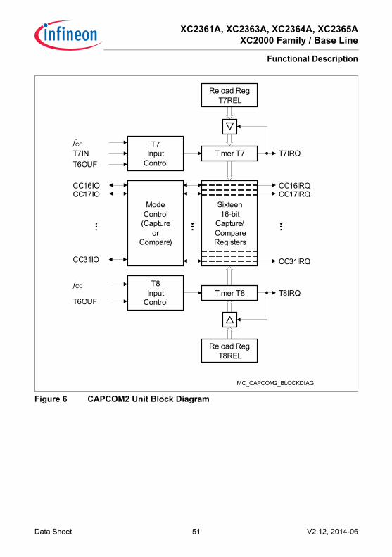
XC2361A, XC2363A, XC2364A, XC2365AXC2000 Family / Base Line
Functional Description
Data Sheet 51 V2.12, 2014-06
Figure 6 CAPCOM2 Unit Block Diagram
Sixteen16-bit
Capture/CompareRegisters
ModeControl
(Captureor
Compare)
T7Input
Control
T8Input
Control
MC_CAPCOM2_BLOCKDIAG
CC16IRQ
CC31IRQ
CC17IRQ
T7IRQ
T8IRQ
CC16IOCC17IO
T7IN
T6OUF
fCC
T6OUF
fCC
Reload Reg.T7REL
Timer T7
Timer T8
Reload Reg.T8REL
CC31IO
XC2361A, XC2363A, XC2364A, XC2365AXC2000 Family / Base Line
Functional Description
Data Sheet 52 V2.12, 2014-06
3.9 Capture/Compare Units CCU6xThe XC236xA types feature the CCU60, CCU61 unit(s).The CCU6 is a high-resolution capture and compare unit with application-specificmodes. It provides inputs to start the timers synchronously, an important feature indevices with several CCU6 modules.The module provides two independent timers (T12, T13), that can be used for PWMgeneration, especially for AC motor control. Additionally, special control modes for blockcommutation and multi-phase machines are supported.
Timer 12 Features• Three capture/compare channels, where each channel can be used either as a
capture or as a compare channel.• Supports generation of a three-phase PWM (six outputs, individual signals for high-
side and low-side switches)• 16-bit resolution, maximum count frequency = peripheral clock• Dead-time control for each channel to avoid short circuits in the power stage• Concurrent update of the required T12/13 registers• Center-aligned and edge-aligned PWM can be generated• Single-shot mode supported• Many interrupt request sources• Hysteresis-like control mode• Automatic start on a HW event (T12HR, for synchronization purposes)
Timer 13 Features• One independent compare channel with one output• 16-bit resolution, maximum count frequency = peripheral clock• Can be synchronized to T12• Interrupt generation at period match and compare match• Single-shot mode supported• Automatic start on a HW event (T13HR, for synchronization purposes)
Additional Features• Block commutation for brushless DC drives implemented• Position detection via Hall sensor pattern• Automatic rotational speed measurement for block commutation• Integrated error handling• Fast emergency stop without CPU load via external signal (CTRAP)• Control modes for multi-channel AC drives• Output levels can be selected and adapted to the power stage

XC2361A, XC2363A, XC2364A, XC2365AXC2000 Family / Base Line
Functional Description
Data Sheet 53 V2.12, 2014-06
Figure 7 CCU6 Block Diagram
Timer T12 can work in capture and/or compare mode for its three channels. The modescan also be combined. Timer T13 can work in compare mode only. The multi-channelcontrol unit generates output patterns that can be modulated by timer T12 and/or timerT13. The modulation sources can be selected and combined for signal modulation.
mc_ccu6_blockdiagram.vsd
Channel 0
Channel 1
Channel 2
T12Dead-time
Control
Input / Output ControlC
C62
COU
T62
CC6
1C
OUT6
1C
C60
COU
T60
COU
T63
CTR
AP
Channel 3T13
CCP
OS0
1
1
1
2221
start
compare
capt
ure
3
Multi-channelControl
TrapControl
compareco
mpa
re
com
pare
com
pare
1
trap
inpu
t
CCP
OS1
CCP
OS2
outpu
t sel
ect
outpu
t sel
ect
3
Hal
l inp
ut
CCU6 Module KernelfSYS
Interrupts
TxHR
XC2361A, XC2363A, XC2364A, XC2365AXC2000 Family / Base Line
Functional Description
Data Sheet 54 V2.12, 2014-06
3.10 General Purpose Timer (GPT12E) UnitThe GPT12E unit is a very flexible multifunctional timer/counter structure which can beused for many different timing tasks such as event timing and counting, pulse width andduty cycle measurements, pulse generation, or pulse multiplication.The GPT12E unit incorporates five 16-bit timers organized in two separate modules,GPT1 and GPT2. Each timer in each module may either operate independently in anumber of different modes or be concatenated with another timer of the same module.Each of the three timers T2, T3, T4 of module GPT1 can be configured individually forone of four basic modes of operation: Timer, Gated Timer, Counter, and IncrementalInterface Mode. In Timer Mode, the input clock for a timer is derived from the systemclock and divided by a programmable prescaler. Counter Mode allows timer clocking inreference to external events.Pulse width or duty cycle measurement is supported in Gated Timer Mode, where theoperation of a timer is controlled by the ‘gate’ level on an external input pin. For thesepurposes each timer has one associated port pin (TxIN) which serves as a gate or clockinput. The maximum resolution of the timers in module GPT1 is 4 system clock cycles.The counting direction (up/down) for each timer can be programmed by software oraltered dynamically by an external signal on a port pin (TxEUD), e.g. to facilitate positiontracking.In Incremental Interface Mode the GPT1 timers can be directly connected to theincremental position sensor signals A and B through their respective inputs TxIN andTxEUD. Direction and counting signals are internally derived from these two inputsignals, so that the contents of the respective timer Tx corresponds to the sensorposition. The third position sensor signal TOP0 can be connected to an interrupt input.Timer T3 has an output toggle latch (T3OTL) which changes its state on each timeroverflow/underflow. The state of this latch may be output on pin T3OUT e.g. for time outmonitoring of external hardware components. It may also be used internally to clocktimers T2 and T4 for measuring long time periods with high resolution.In addition to the basic operating modes, T2 and T4 may be configured as reload orcapture register for timer T3. A timer used as capture or reload register is stopped. Thecontents of timer T3 is captured into T2 or T4 in response to a signal at the associatedinput pin (TxIN). Timer T3 is reloaded with the contents of T2 or T4, triggered either byan external signal or a selectable state transition of its toggle latch T3OTL. When bothT2 and T4 are configured to alternately reload T3 on opposite state transitions of T3OTLwith the low and high times of a PWM signal, this signal can be continuously generatedwithout software intervention.
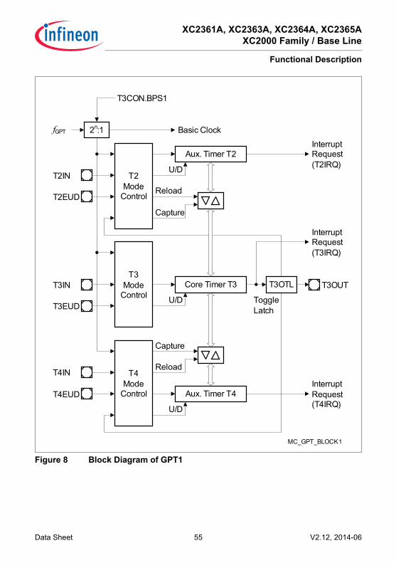
XC2361A, XC2363A, XC2364A, XC2365AXC2000 Family / Base Line
Functional Description
Data Sheet 55 V2.12, 2014-06
Figure 8 Block Diagram of GPT1
MC_GPT_BLOCK1
Aux. Timer T2
2n:1
T2Mode
Control
Capture
U/D
Basic ClockfGPT
T3CON.BPS1
T3OTL T3OUT
Toggle Latch
T2IN
T2EUDReload
Core Timer T3T3
ModeControl
T3IN
T3EUDU/D
InterruptRequest(T3IRQ)
T4Mode
Control
U/D
Aux. Timer T4T4EUD
T4INReload
Capture
InterruptRequest(T4IRQ)
InterruptRequest(T2IRQ)
XC2361A, XC2363A, XC2364A, XC2365AXC2000 Family / Base Line
Functional Description
Data Sheet 56 V2.12, 2014-06
With its maximum resolution of 2 system clock cycles, the GPT2 module providesprecise event control and time measurement. It includes two timers (T5, T6) and acapture/reload register (CAPREL). Both timers can be clocked with an input clock whichis derived from the CPU clock via a programmable prescaler or with external signals. Thecounting direction (up/down) for each timer can be programmed by software or altereddynamically with an external signal on a port pin (TxEUD1)). Concatenation of the timersis supported with the output toggle latch (T6OTL) of timer T6, which changes its state oneach timer overflow/underflow.The state of this latch may be used to clock timer T5, and/or it may be output on pinT6OUT. The overflows/underflows of timer T6 can also be used to clock the CAPCOM2timers and to initiate a reload from the CAPREL register.The CAPREL register can capture the contents of timer T5 based on an external signaltransition on the corresponding port pin (CAPIN); timer T5 may optionally be clearedafter the capture procedure. This allows the XC236xA to measure absolute timedifferences or to perform pulse multiplication without software overhead.The capture trigger (timer T5 to CAPREL) can also be generated upon transitions ofGPT1 timer T3 inputs T3IN and/or T3EUD. This is especially advantageous when T3operates in Incremental Interface Mode.
1) Exception: T5EUD is not connected to a pin.

XC2361A, XC2363A, XC2364A, XC2365AXC2000 Family / Base Line
Functional Description
Data Sheet 57 V2.12, 2014-06
Figure 9 Block Diagram of GPT2
MC_GPT_BLOCK2
GPT2 Timer T5
2n:1
T5Mode
Control
GPT2 CAPREL
T3IN/T3EUD
CAPRELMode
Control
T6Mode
Control
Reload
Clear
U/D
Capture
Clear
U/DT5IN
CAPIN
InterruptRequest(T5IRQ)
InterruptRequest(T6IRQ)
InterruptRequest(CRIRQ)
Basic ClockfGPT
T6CON.BPS2
T6IN
GPT2 Timer T6 T6OTL T6OUT
T6OUF
Toggle FF
T6EUD
T5EUD

XC2361A, XC2363A, XC2364A, XC2365AXC2000 Family / Base Line
Functional Description
Data Sheet 58 V2.12, 2014-06
3.11 Real Time ClockThe Real Time Clock (RTC) module of the XC236xA can be clocked with a clock signalselected from internal sources or external sources (pins).The RTC basically consists of a chain of divider blocks:• Selectable 32:1 and 8:1 dividers (on - off)• The reloadable 16-bit timer T14• The 32-bit RTC timer block (accessible via registers RTCH and RTCL) consisting of:
– a reloadable 10-bit timer– a reloadable 6-bit timer– a reloadable 6-bit timer– a reloadable 10-bit timer
All timers count up. Each timer can generate an interrupt request. All requests arecombined to a common node request.
Figure 10 RTC Block Diagram
Note: The registers associated with the RTC are only affected by a power reset.
CNT-Register
REL-Register
10 Bits6 Bits6 Bits10 BitsT14
MCB05568B
T14-Register
Interrupt Sub NodeRTCINT
MUX 32
PRE
RUN
CNTINT3
CNTINT2
CNTINT1
CNTINT0
fCNT
fRTC
T14REL 10 Bits6 Bits6 Bits10 Bits
:
MUX 8:
REFCLK

XC2361A, XC2363A, XC2364A, XC2365AXC2000 Family / Base Line
Functional Description
Data Sheet 59 V2.12, 2014-06
The RTC module can be used for different purposes:• System clock to determine the current time and date• Cyclic time-based interrupt, to provide a system time tick independent of CPU
frequency and other resources• 48-bit timer for long-term measurements• Alarm interrupt at a defined time

XC2361A, XC2363A, XC2364A, XC2365AXC2000 Family / Base Line
Functional Description
Data Sheet 60 V2.12, 2014-06
3.12 A/D ConvertersFor analog signal measurement, up to two 10-bit A/D converters (ADC0, ADC1) with11 + 5 multiplexed input channels and a sample and hold circuit have been integratedon-chip. 4 inputs can be converted by both A/D converters. Conversions use thesuccessive approximation method. The sample time (to charge the capacitors) and theconversion time are programmable so that they can be adjusted to the external circuit.The A/D converters can also operate in 8-bit conversion mode, further reducing theconversion time.Several independent conversion result registers, selectable interrupt requests, andhighly flexible conversion sequences provide a high degree of programmability to meetthe application requirements. Both modules can be synchronized to allow parallelsampling of two input channels.For applications that require more analog input channels, external analog multiplexerscan be controlled automatically. For applications that require fewer analog inputchannels, the remaining channel inputs can be used as digital input port pins.The A/D converters of the XC236xA support two types of request sources which can betriggered by several internal and external events.• Parallel requests are activated at the same time and then executed in a predefined
sequence.• Queued requests are executed in a user-defined sequence.In addition, the conversion of a specific channel can be inserted into a running sequencewithout disturbing that sequence. All requests are arbitrated according to the prioritylevel assigned to them.Data reduction features reduce the number of required CPU access operations allowingthe precise evaluation of analog inputs (high conversion rate) even at a low CPU speed.Result data can be reduced by limit checking or accumulation of results.The Peripheral Event Controller (PEC) can be used to control the A/D converters or toautomatically store conversion results to a table in memory for later evaluation, withoutrequiring the overhead of entering and exiting interrupt routines for each data transfer.Each A/D converter contains eight result registers which can be concatenated to build aresult FIFO. Wait-for-read mode can be enabled for each result register to prevent theloss of conversion data.In order to decouple analog inputs from digital noise and to avoid input trigger noise,those pins used for analog input can be disconnected from the digital input stages. Thiscan be selected for each pin separately with the Port x Digital Input Disable registers.The Auto-Power-Down feature of the A/D converters minimizes the power consumptionwhen no conversion is in progress.Broken wire detection for each channel and a multiplexer test mode provide informationto verify the proper operation of the analog signal sources (e.g. a sensor system).
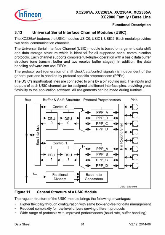
XC2361A, XC2363A, XC2364A, XC2365AXC2000 Family / Base Line
Functional Description
Data Sheet 61 V2.12, 2014-06
3.13 Universal Serial Interface Channel Modules (USIC)The XC236xA features the USIC modules USIC0, USIC1, USIC2. Each module providestwo serial communication channels.The Universal Serial Interface Channel (USIC) module is based on a generic data shiftand data storage structure which is identical for all supported serial communicationprotocols. Each channel supports complete full-duplex operation with a basic data bufferstructure (one transmit buffer and two receive buffer stages). In addition, the datahandling software can use FIFOs.The protocol part (generation of shift clock/data/control signals) is independent of thegeneral part and is handled by protocol-specific preprocessors (PPPs).The USIC’s input/output lines are connected to pins by a pin routing unit. The inputs andoutputs of each USIC channel can be assigned to different interface pins, providing greatflexibility to the application software. All assignments can be made during runtime.
Figure 11 General Structure of a USIC Module
The regular structure of the USIC module brings the following advantages:• Higher flexibility through configuration with same look-and-feel for data management• Reduced complexity for low-level drivers serving different protocols• Wide range of protocols with improved performances (baud rate, buffer handling)
USIC_basic.vsd
Bus
Inte
rfac
e
DBU0
DBU1
Control 0
Control 1
DSU0
DSU1
PPP_APPP_BPPP_CPPP_D
PPP_APPP_BPPP_CPPP_D
Pin
Rou
ting
She
ll
Buffer & Shift Structure Protocol Preprocessors PinsBus
fsys FractionalDividers
Baud rateGenerators

XC2361A, XC2363A, XC2364A, XC2365AXC2000 Family / Base Line
Functional Description
Data Sheet 62 V2.12, 2014-06
Target ProtocolsEach USIC channel can receive and transmit data frames with a selectable data wordwidth from 1 to 16 bits in each of the following protocols:• UART (asynchronous serial channel)
– module capability: maximum baud rate = fSYS / 4– data frame length programmable from 1 to 63 bits– MSB or LSB first
• LIN Support (Local Interconnect Network)– module capability: maximum baud rate = fSYS / 16– checksum generation under software control– baud rate detection possible by built-in capture event of baud rate generator
• SSC/SPI (synchronous serial channel with or without data buffer)– module capability: maximum baud rate = fSYS / 2, limited by loop delay– number of data bits programmable from 1 to 63, more with explicit stop condition– MSB or LSB first– optional control of slave select signals
• IIC (Inter-IC Bus)– supports baud rates of 100 kbit/s and 400 kbit/s
• IIS (Inter-IC Sound Bus)– module capability: maximum baud rate = fSYS / 2
Note: Depending on the selected functions (such as digital filters, input synchronizationstages, sample point adjustment, etc.), the maximum achievable baud rate can belimited. Please note that there may be additional delays, such as internal orexternal propagation delays and driver delays (e.g. for collision detection in UARTmode, for IIC, etc.).
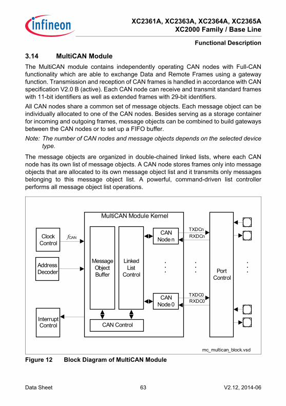
XC2361A, XC2363A, XC2364A, XC2365AXC2000 Family / Base Line
Functional Description
Data Sheet 63 V2.12, 2014-06
3.14 MultiCAN ModuleThe MultiCAN module contains independently operating CAN nodes with Full-CANfunctionality which are able to exchange Data and Remote Frames using a gatewayfunction. Transmission and reception of CAN frames is handled in accordance with CANspecification V2.0 B (active). Each CAN node can receive and transmit standard frameswith 11-bit identifiers as well as extended frames with 29-bit identifiers.All CAN nodes share a common set of message objects. Each message object can beindividually allocated to one of the CAN nodes. Besides serving as a storage containerfor incoming and outgoing frames, message objects can be combined to build gatewaysbetween the CAN nodes or to set up a FIFO buffer.Note: The number of CAN nodes and message objects depends on the selected device
type.
The message objects are organized in double-chained linked lists, where each CANnode has its own list of message objects. A CAN node stores frames only into messageobjects that are allocated to its own message object list and it transmits only messagesbelonging to this message object list. A powerful, command-driven list controllerperforms all message object list operations.
Figure 12 Block Diagram of MultiCAN Modulemc_multican_block.vsd
MultiCAN Module Kernel
InterruptControl
fCAN
PortControl
CAN Control
MessageObjectBuffer
CANNode 0
LinkedList
Control
ClockControl
AddressDecoder
CANNode n
TXDCnRXDCn
TXDC0RXDC0
...
...
...

XC2361A, XC2363A, XC2364A, XC2365AXC2000 Family / Base Line
Functional Description
Data Sheet 64 V2.12, 2014-06
MultiCAN Features• CAN functionality conforming to CAN specification V2.0 B active for each CAN node
(compliant to ISO 11898)• Independent CAN nodes• Set of independent message objects (shared by the CAN nodes)• Dedicated control registers for each CAN node• Data transfer rate up to 1 Mbit/s, individually programmable for each node• Flexible and powerful message transfer control and error handling capabilities• Full-CAN functionality for message objects:
– Can be assigned to one of the CAN nodes– Configurable as transmit or receive objects, or as message buffer FIFO– Handle 11-bit or 29-bit identifiers with programmable acceptance mask for filtering– Remote Monitoring Mode, and frame counter for monitoring
• Automatic Gateway Mode support• 16 individually programmable interrupt nodes• Analyzer mode for CAN bus monitoring
3.15 System TimerThe System Timer consists of a programmable prescaler and two concatenated timers(10 bits and 6 bits). Both timers can generate interrupt requests. The clock source canbe selected and the timers can also run during power reduction modes.Therefore, the System Timer enables the software to maintain the current time forscheduling functions or for the implementation of a clock.

XC2361A, XC2363A, XC2364A, XC2365AXC2000 Family / Base Line
Functional Description
Data Sheet 65 V2.12, 2014-06
3.16 Watchdog TimerThe Watchdog Timer is one of the fail-safe mechanisms which have been implementedto prevent the controller from malfunctioning for longer periods of time.The Watchdog Timer is always enabled after an application reset of the chip. It can bedisabled and enabled at any time by executing the instructions DISWDT and ENWDTrespectively. The software has to service the Watchdog Timer before it overflows. If thisis not the case because of a hardware or software failure, the Watchdog Timeroverflows, generating a prewarning interrupt and then a reset request.The Watchdog Timer is a 16-bit timer clocked with the system clock divided by 16,384or 256. The Watchdog Timer register is set to a prespecified reload value (stored inWDTREL) in order to allow further variation of the monitored time interval. Each time itis serviced by the application software, the Watchdog Timer is reloaded and theprescaler is cleared.Time intervals between 3.2 μs and 13.42 s can be monitored (@ 80 MHz).The default Watchdog Timer interval after power-up is 6.5 ms (@ 10 MHz).
3.17 Clock GenerationThe Clock Generation Unit can generate the system clock signal fSYS for the XC236xAfrom a number of external or internal clock sources:• External clock signals with pad voltage or core voltage levels• External crystal or resonator using the on-chip oscillator• On-chip clock source for operation without crystal/resonator• Wake-up clock (ultra-low-power) to further reduce power consumptionThe programmable on-chip PLL with multiple prescalers generates a clock signal formaximum system performance from standard crystals, a clock input signal, or from theon-chip clock source. See also Section 4.6.2.The Oscillator Watchdog (OWD) generates an interrupt if the crystal oscillator frequencyfalls below a certain limit or stops completely. In this case, the system can be suppliedwith an emergency clock to enable operation even after an external clock failure.All available clock signals can be output on one of two selectable pins.
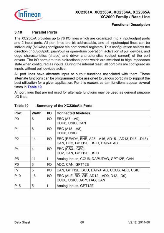
XC2361A, XC2363A, XC2364A, XC2365AXC2000 Family / Base Line
Functional Description
Data Sheet 66 V2.12, 2014-06
3.18 Parallel PortsThe XC236xA provides up to 76 I/O lines which are organized into 7 input/output portsand 2 input ports. All port lines are bit-addressable, and all input/output lines can beindividually (bit-wise) configured via port control registers. This configuration selects thedirection (input/output), push/pull or open-drain operation, activation of pull devices, andedge characteristics (shape) and driver characteristics (output current) of the portdrivers. The I/O ports are true bidirectional ports which are switched to high impedancestate when configured as inputs. During the internal reset, all port pins are configured asinputs without pull devices active.All port lines have alternate input or output functions associated with them. Thesealternate functions can be programmed to be assigned to various port pins to support thebest utilization for a given application. For this reason, certain functions appear severaltimes in Table 10.All port lines that are not used for alternate functions may be used as general purposeI/O lines.
Table 10 Summary of the XC236xA’s Ports
Port Width I/O Connected ModulesP0 8 I/O EBC (A7…A0),
CCU6, USIC, CANP1 8 I/O EBC (A15…A8),
CCU6, USICP2 14 I/O EBC (READY, BHE, A23…A16, AD15…AD13, D15…D13),
CAN, CC2, GPT12E, USIC, DAP/JTAGP4 4 I/O EBC (CS3…CS0),
CC2, CAN, GPT12E, USICP5 11 I Analog Inputs, CCU6, DAP/JTAG, GPT12E, CANP6 3 I/O ADC, CAN, GPT12EP7 5 I/O CAN, GPT12E, SCU, DAP/JTAG, CCU6, ADC, USICP10 16 I/O EBC (ALE, RD, WR, AD12…AD0, D12…D0),
CCU6, USIC, DAP/JTAG, CANP15 5 I Analog Inputs, GPT12E
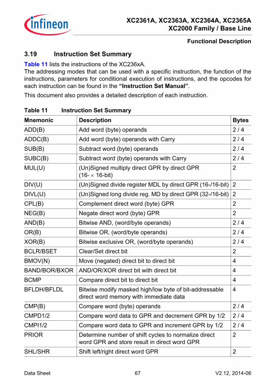
XC2361A, XC2363A, XC2364A, XC2365AXC2000 Family / Base Line
Functional Description
Data Sheet 67 V2.12, 2014-06
3.19 Instruction Set SummaryTable 11 lists the instructions of the XC236xA.The addressing modes that can be used with a specific instruction, the function of theinstructions, parameters for conditional execution of instructions, and the opcodes foreach instruction can be found in the “Instruction Set Manual”.This document also provides a detailed description of each instruction.
Table 11 Instruction Set SummaryMnemonic Description BytesADD(B) Add word (byte) operands 2 / 4ADDC(B) Add word (byte) operands with Carry 2 / 4SUB(B) Subtract word (byte) operands 2 / 4SUBC(B) Subtract word (byte) operands with Carry 2 / 4MUL(U) (Un)Signed multiply direct GPR by direct GPR
(16- × 16-bit)2
DIV(U) (Un)Signed divide register MDL by direct GPR (16-/16-bit) 2DIVL(U) (Un)Signed long divide reg. MD by direct GPR (32-/16-bit) 2CPL(B) Complement direct word (byte) GPR 2NEG(B) Negate direct word (byte) GPR 2AND(B) Bitwise AND, (word/byte operands) 2 / 4OR(B) Bitwise OR, (word/byte operands) 2 / 4XOR(B) Bitwise exclusive OR, (word/byte operands) 2 / 4BCLR/BSET Clear/Set direct bit 2BMOV(N) Move (negated) direct bit to direct bit 4BAND/BOR/BXOR AND/OR/XOR direct bit with direct bit 4BCMP Compare direct bit to direct bit 4BFLDH/BFLDL Bitwise modify masked high/low byte of bit-addressable
direct word memory with immediate data4
CMP(B) Compare word (byte) operands 2 / 4CMPD1/2 Compare word data to GPR and decrement GPR by 1/2 2 / 4CMPI1/2 Compare word data to GPR and increment GPR by 1/2 2 / 4PRIOR Determine number of shift cycles to normalize direct
word GPR and store result in direct word GPR2
SHL/SHR Shift left/right direct word GPR 2

XC2361A, XC2363A, XC2364A, XC2365AXC2000 Family / Base Line
Functional Description
Data Sheet 68 V2.12, 2014-06
ROL/ROR Rotate left/right direct word GPR 2ASHR Arithmetic (sign bit) shift right direct word GPR 2MOV(B) Move word (byte) data 2 / 4MOVBS/Z Move byte operand to word op. with sign/zero extension 2 / 4JMPA/I/R Jump absolute/indirect/relative if condition is met 4JMPS Jump absolute to a code segment 4JB(C) Jump relative if direct bit is set (and clear bit) 4JNB(S) Jump relative if direct bit is not set (and set bit) 4CALLA/I/R Call absolute/indirect/relative subroutine if condition is met 4CALLS Call absolute subroutine in any code segment 4PCALL Push direct word register onto system stack and call
absolute subroutine4
TRAP Call interrupt service routine via immediate trap number 2PUSH/POP Push/pop direct word register onto/from system stack 2SCXT Push direct word register onto system stack and update
register with word operand4
RET(P) Return from intra-segment subroutine(and pop direct word register from system stack)
2
RETS Return from inter-segment subroutine 2RETI Return from interrupt service subroutine 2SBRK Software Break 2SRST Software Reset 4IDLE Enter Idle Mode 4PWRDN Unused instruction1) 4SRVWDT Service Watchdog Timer 4DISWDT/ENWDT Disable/Enable Watchdog Timer 4EINIT End-of-Initialization Register Lock 4ATOMIC Begin ATOMIC sequence 2EXTR Begin EXTended Register sequence 2EXTP(R) Begin EXTended Page (and Register) sequence 2 / 4EXTS(R) Begin EXTended Segment (and Register) sequence 2 / 4
Table 11 Instruction Set Summary (cont’d)
Mnemonic Description Bytes
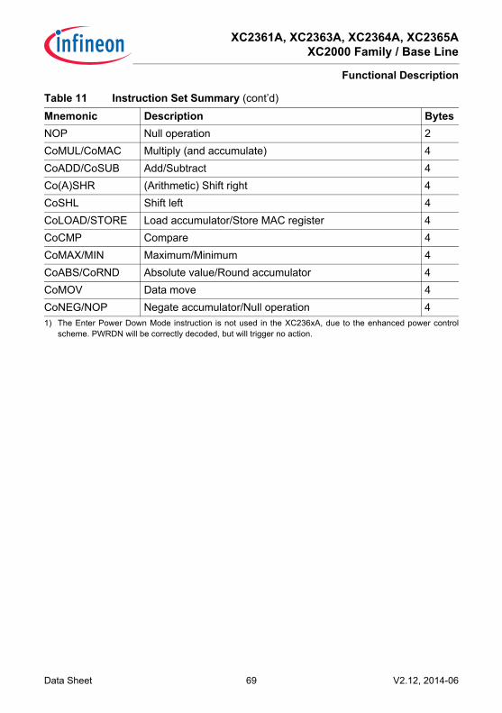
XC2361A, XC2363A, XC2364A, XC2365AXC2000 Family / Base Line
Functional Description
Data Sheet 69 V2.12, 2014-06
NOP Null operation 2CoMUL/CoMAC Multiply (and accumulate) 4CoADD/CoSUB Add/Subtract 4Co(A)SHR (Arithmetic) Shift right 4CoSHL Shift left 4CoLOAD/STORE Load accumulator/Store MAC register 4CoCMP Compare 4CoMAX/MIN Maximum/Minimum 4CoABS/CoRND Absolute value/Round accumulator 4CoMOV Data move 4CoNEG/NOP Negate accumulator/Null operation 41) The Enter Power Down Mode instruction is not used in the XC236xA, due to the enhanced power control
scheme. PWRDN will be correctly decoded, but will trigger no action.
Table 11 Instruction Set Summary (cont’d)
Mnemonic Description Bytes

XC2361A, XC2363A, XC2364A, XC2365AXC2000 Family / Base Line
Electrical Parameters
Data Sheet 70 V2.12, 2014-06
4 Electrical ParametersThe operating range for the XC236xA is defined by its electrical parameters. For properoperation the specified limits must be respected when integrating the device in its targetenvironment.
4.1 General ParametersThese parameters are valid for all subsequent descriptions, unless otherwise noted.
4.1.1 Absolut Maximum Rating ConditionsStresses above the values listed under “Absolute Maximum Ratings” may causepermanent damage to the device. This is a stress rating only. Functional operation of thedevice at these or any other conditions above those indicated in the operational sectionsof this specification is not implied. Exposure to absolute maximum rating conditions foran extended time may affect device reliability.During absolute maximum rating overload conditions (VIN > VDDP or VIN < VSS) thevoltage on VDDP pins with respect to ground (VSS) must not exceed the values defined bythe absolute maximum ratings.
Table 12 Absolute Maximum Rating ParametersParameter Symbol Values Unit Note /
Test ConditionMin. Typ. Max.Output current on a pin when high value is driven
IOH SR -30 − − mA
Output current on a pin when low value is driven
IOL SR − − 30 mA
Overload current IOV SR -10 − 10 mA 1)
1) Overload condition occurs if the input voltage VIN is out of the absolute maximum rating range. In this case thecurrent must be limited to the listed values by design measures.
Absolute sum of overload currents
Σ|IOV| SR
− − 100 mA 1)
Junction Temperature TJ SR -40 − 150 °CStorage Temperature TST SR -65 − 150 °CDigital supply voltage for IO pads and voltage regulators
VDDPA, VDDPB SR
-0.5 − 6.0 V
Voltage on any pin with respect to ground (Vss)
VIN SR -0.5 − VDDP+ 0.5
V VIN ≤ VDDP(max)
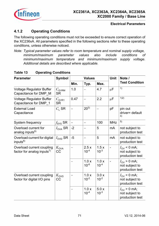
XC2361A, XC2363A, XC2364A, XC2365AXC2000 Family / Base Line
Electrical Parameters
Data Sheet 71 V2.12, 2014-06
4.1.2 Operating ConditionsThe following operating conditions must not be exceeded to ensure correct operation ofthe XC236xA. All parameters specified in the following sections refer to these operatingconditions, unless otherwise noticed.Note: Typical parameter values refer to room temperature and nominal supply voltage,
minimum/maximum parameter values also include conditions ofminimum/maximum temperature and minimum/maximum supply voltage.Additional details are described where applicable.
Table 13 Operating ConditionsParameter Symbol Values Unit Note /
Test ConditionMin. Typ. Max.Voltage Regulator Buffer Capacitance for DMP_M
CEVRM SR
1.0 − 4.7 μF 1)
Voltage Regulator Buffer Capacitance for DMP_1
CEVR1 SR
0.47 − 2.2 μF 1)2)
External Load Capacitance
CL SR − 203) − pF pin out driver= default4)
System frequency fSYS SR − − 100 MHz 5)
Overload current for analog inputs6)
IOVA SR -2 − 5 mA not subject to production test
Overload current for digital inputs6)
IOVD SR -5 − 5 mA not subject to production test
Overload current coupling factor for analog inputs7)
KOVA CC
− 2.5 x 10⁻⁴
1.5 x 10⁻³
- IOV < 0 mA;not subject to production test
− 1.0 x 10⁻⁶
1.0 x 10⁻⁴
- IOV > 0 mA;not subject to production test
Overload current coupling factor for digital I/O pins
KOVD CC
− 1.0 x 10⁻²
3.0 x 10⁻²
IOV < 0 mA;not subject to production test
− 1.0 x 10⁻⁴
5.0 x 10⁻³
IOV > 0 mA;not subject to production test

XC2361A, XC2363A, XC2364A, XC2365AXC2000 Family / Base Line
Electrical Parameters
Data Sheet 72 V2.12, 2014-06
Absolute sum of overload currents
Σ|IOV| SR
− − 50 mA not subject to production test
Digital core supply voltage for domain M8)
VDDIM CC
− 1.5 −
Digital core supply voltage for domain 18)
VDDI1 CC
− 1.5 −
Digital supply voltage for IO pads and voltage regulators
VDDP SR 4.5 − 5.5 V
Digital ground voltage VSS SR − 0 − V1) To ensure the stability of the voltage regulators the EVRs must be buffered with ceramic capacitors. Separate
buffer capacitors with the recomended values shall be connected as close as possible to each VDDIM and VDDI1pin to keep the resistance of the board tracks below 2 Ohm. Connect all VDDI1 pins together. The minimumcapacitance value is required for proper operation under all conditions (e.g. temperature). Higher valuesslightly increase the startup time.
2) Use one Capacitor for each pin.3) This is the reference load. For bigger capacitive loads, use the derating factors listed in the PAD properties
section.4) The timing is valid for pin drivers operating in default current mode (selected after reset). Reducing the output
current may lead to increased delays or reduced driving capability (CL).5) The operating frequency range may be reduced for specific device types. This is indicated in the device
designation (...FxxL). 80 MHz devices are marked ...F80L.6) Overload conditions occur if the standard operating conditions are exceeded, i.e. the voltage on any pin
exceeds the specified range: VOV > VIHmax (IOV > 0) or VOV < VILmin ((IOV < 0). The absolute sum of inputoverload currents on all pins may not exceed 50 mA. The supply voltages must remain within the specifiedlimits. Proper operation under overload conditions depends on the application. Overload conditions must notoccur on pin XTAL1 (powered by VDDIM).
7) An overload current (IOV) through a pin injects a certain error current (IINJ) into the adjacent pins. This errorcurrent adds to the respective pins leakage current (IOZ). The amount of error current depends on the overloadcurrent and is defined by the overload coupling factor KOV. The polarity of the injected error current is inversecompared to the polarity of the overload current that produces it.The total current through a pin is |ITOT| = |IOZ|+ (|IOV| KOV). The additional error current may distort the input voltage on analog inputs.
8) Value is controlled by on-chip regulator
Table 13 Operating Conditions (cont’d)
Parameter Symbol Values Unit Note / Test ConditionMin. Typ. Max.
XC2361A, XC2363A, XC2364A, XC2365AXC2000 Family / Base Line
Electrical Parameters
Data Sheet 73 V2.12, 2014-06
4.1.3 Pad Timing DefinitionIf not otherwise noted, all timing parameters are tested and are valid for thecorresponding output pins operating in strong driver, fast edge mode.See also “Pad Properties” on Page 102.
4.1.4 Parameter InterpretationThe parameters listed in the following include both the characteristics of the XC236xAand its demands on the system. To aid in correctly interpreting the parameters whenevaluating them for a design, they are marked accordingly in the column “Symbol”:CC (Controller Characteristics):The logic of the XC236xA provides signals with the specified characteristics.SR (System Requirement):The external system must provide signals with the specified characteristics to theXC236xA.
XC2361A, XC2363A, XC2364A, XC2365AXC2000 Family / Base Line
Electrical Parameters
Data Sheet 74 V2.12, 2014-06
4.2 DC ParametersThese parameters are static or average values that may be exceeded during switchingtransitions (e.g. output current).Leakage current is strongly dependent on the operating temperature and the voltagelevel at the respective pin. The maximum values in the following tables apply under worstcase conditions, i.e. maximum temperature and an input level equal to the supplyvoltage.The value for the leakage current in an application can be determined by using therespective leakage derating formula (see tables) with values from that application.The pads of the XC236xA are designed to operate in various driver modes. The DCparameter specifications refer to the pad current limits specified in Section 4.6.4.
Supply Voltage RestrictionsThe XC236xA can operate within a wide supply voltage range from 3.0 V to 5.5 V.However, during operation this supply voltage must remain within 10 percent of theselected nominal supply voltage. It cannot vary across the full operating voltage range.Because of the supply voltage restriction and because electrical behavior depends onthe supply voltage, the parameters are specified separately for the upper and the lowervoltage range.During operation, the supply voltages may only change with a maximum speed ofdV/dt < 1 V/ms.During power-on sequences, the supply voltages may only change with a maximumspeed of dV/dt < 5 V/μs, i.e. the target supply voltage may be reached earliest afterapprox. 1 μs.Note: To limit the speed of supply voltage changes, the employment of external buffer
capacitors at pins VDDPA/VDDPB is recommended.

XC2361A, XC2363A, XC2364A, XC2365AXC2000 Family / Base Line
Electrical Parameters
Data Sheet 75 V2.12, 2014-06
Pullup/Pulldown Device BehaviorMost pins of the XC236xA feature pullup or pulldown devices. For some special pinsthese are fixed; for the port pins they can be selected by the application.The specified current values indicate how to load the respective pin depending on theintended signal level. Figure 13 shows the current paths.The shaded resistors shown in the figure may be required to compensate system pullcurrents that do not match the given limit values.
Figure 13 Pullup/Pulldown Current Definition
MC_XC2X_PULL
VDDP
VSS
Pullup
Pulldown

XC2361A, XC2363A, XC2364A, XC2365AXC2000 Family / Base Line
Electrical Parameters
Data Sheet 76 V2.12, 2014-06
4.2.1 DC ParametersKeeping signal levels within the limits specified in this table ensures operation withoutoverload conditions. For signal levels outside these specifications, also refer to thespecification of the overload current IOV.Note: Operating Conditions apply.
Table 14 is valid under the following conditions:VDDP ≥ 4.5 V; VDDPtyp = 5 V; VDDP ≤ 5.5 V
Table 14 DC Characteristics for Upper Voltage RangeParameter Symbol Values Unit Note /
Test ConditionMin. Typ. Max.Pin capacitance (digital inputs/outputs). To be doubled for double bond pins.1)
CIO CC − − 10 pF not subject to production test
Input Hysteresis2) HYS CC 0.11 x VDDP
− − V RS = 0 Ohm
Absolute input leakage current on pins of analog ports3)
|IOZ1| CC
− 10 200 nA VIN > 0 V;VIN < VDDP
Absolute input leakage current for all other pins. To be doubled for double bond pins.3)1)4)
|IOZ2| CC
− 0.2 5 μA TJ ≤ 110 °C;VIN < VDDP;VIN > VSS
− 0.2 15 μA TJ≤ 150 °C;VIN < VDDP;VIN > VSS
Pull Level Force Current5) |IPLF| SR 250 − − μA 6)
Pull Level Keep Current7) |IPLK| SR
− − 30 μA 6)
Input high voltage(all except XTAL1)
VIH SR 0.7 x VDDP
− VDDP+ 0.3
V
Input low voltage(all except XTAL1)
VIL SR -0.3 − 0.3 x VDDP
V
Output High voltage8) VOH CC VDDP- 1.0
− − V IOH ≥ IOHmax
VDDP- 0.4
− − V IOH ≥ IOHnom9)

XC2361A, XC2363A, XC2364A, XC2365AXC2000 Family / Base Line
Electrical Parameters
Data Sheet 77 V2.12, 2014-06
Output Low Voltage8) VOL CC − − 1.0 V IOL ≤ IOLmax
− − 0.4 V IOL ≤ IOLnom9)
1) Because each double bond pin is connected to two pads (standard pad and high-speed pad), it has twice thenormal value. For a list of affected pins refer to the pin definitions table in chapter 2.
2) Not subject to production test - verified by design/characterization. Hysteresis is implemented to avoidmetastable states and switching due to internal ground bounce. It cannot suppress switching due to externalsystem noise under all conditions.
3) If the input voltage exceeds the respective supply voltage due to ground bouncing (VIN < VSS) or supply ripple(VIN > VDDP), a certain amount of current may flow through the protection diodes. This current adds to theleakage current. An additional error current (IINJ) will flow if an overload current flows through an adjacent pin.Please refer to the definition of the overload coupling factor KOV.
4) The given values are worst-case values. In production test, this leakage current is only tested at 125 °C; othervalues are ensured by correlation. For derating, please refer to the following descriptions: Leakage deratingdepending on temperature (TJ = junction temperature [°C]): IOZ = 0.05 x e(1.5 + 0.028 x TJ>) [μA]. For example, ata temperature of 95 °C the resulting leakage current is 3.2 μA. Leakage derating depending on voltage level(DV = VDDP - VPIN [V]): IOZ = IOZtempmax - (1.6 x DV) (μA]. This voltage derating formula is an approximationwhich applies for maximum temperature.
5) Drive the indicated minimum current through this pin to change the default pin level driven by the enabled pulldevice: VPIN ≤ VILmax for a pullup; VPIN ≥ VIHmin for a pulldown.
6) These values apply to the fixed pull-devices in dedicated pins and to the user-selectable pull-devices ingeneral purpose IO pins.
7) Limit the current through this pin to the indicated value so that the enabled pull device can keep the defaultpin level: VPIN ≥ VIHmin for a pullup; VPIN ≤ VILmax for a pulldown.
8) The maximum deliverable output current of a port driver depends on the selected output driver mode. Thisspecification is not valid for outputs which are switched to open drain mode. In this case the respective outputwill float and the voltage is determined by the external circuit.
9) As a rule, with decreasing output current the output levels approach the respective supply level (VOL->VSS,VOH->VDDP). However, only the levels for nominal output currents are verified.
Table 14 DC Characteristics for Upper Voltage Range (cont’d)
Parameter Symbol Values Unit Note / Test ConditionMin. Typ. Max.

XC2361A, XC2363A, XC2364A, XC2365AXC2000 Family / Base Line
Electrical Parameters
Data Sheet 78 V2.12, 2014-06
4.2.2 DC Parameters for Lower Voltage AreaKeeping signal levels within the limits specified in this table ensures operation withoutoverload conditions. For signal levels outside these specifications, also refer to thespecification of the overload current IOV.Note: Operating Conditions apply.
Table 15 is valid under the following conditions:VDDP ≥ 3.0 V; VDDPtyp = 3.3 V; VDDP ≤ 4.5 V
Table 15 DC Characteristics for Lower Voltage RangeParameter Symbol Values Unit Note /
Test ConditionMin. Typ. Max.Pin capacitance (digital inputs/outputs). To be doubled for double bond pins.1)
CIO CC − − 10 pF not subject to production test
Input Hysteresis2) HYS CC 0.07 x VDDP
− − V RS = 0 Ohm
Absolute input leakage current on pins of analog ports3)
|IOZ1| CC
− 10 200 nA VIN > VSS;VIN < VDDP
Absolute input leakage current for all other pins. To be doubled for double bond pins.3)1)4)
|IOZ2| CC
− 0.2 2.5 μA TJ ≤ 110 °C;VIN < VDDP;VIN > VSS
− 0.2 8 μA TJ ≤ 150 °C;VIN < VDDP;VIN > VSS
Pull Level Force Current5) |IPLF| SR 150 − − 6)
Pull Level Keep Current7) |IPLK| SR
− − 10 μA 6)
Input high voltage(all except XTAL1)
VIH SR 0.7 x VDDP
− VDDP+ 0.3
V
Input low voltage(all except XTAL1)
VIL SR -0.3 − 0.3 x VDDP
V
Output High voltage8) VOH CC VDDP- 1.0
− − V IOH ≥ IOHmax
VDDP- 0.4
− − V IOH ≥ IOHnom9)

XC2361A, XC2363A, XC2364A, XC2365AXC2000 Family / Base Line
Electrical Parameters
Data Sheet 79 V2.12, 2014-06
Output Low Voltage8) VOL CC − − 1.0 V IOL ≤ IOLmax
− − 0.4 V IOL ≤ IOLnom10)
1) Because each double bond pin is connected to two pads (standard pad and high-speed pad), it has twice thenormal value. For a list of affected pins refer to the pin definitions table in chapter 2.
2) Not subject to production test - verified by design/characterization. Hysteresis is implemented to avoidmetastable states and switching due to internal ground bounce. It cannot suppress switching due to externalsystem noise under all conditions.
3) If the input voltage exceeds the respective supply voltage due to ground bouncing (VIN < VSS) or supply ripple(VIN > VDDP), a certain amount of current may flow through the protection diodes. This current adds to theleakage current. An additional error current (IINJ) will flow if an overload current flows through an adjacent pin.Please refer to the definition of the overload coupling factor KOV.
4) The given values are worst-case values. In production test, this leakage current is only tested at 125 °C; othervalues are ensured by correlation. For derating, please refer to the following descriptions: Leakage deratingdepending on temperature (TJ = junction temperature [°C]): IOZ = 0.05 x e(1.5 + 0.028 x TJ>) [μA]. For example, ata temperature of 95 °C the resulting leakage current is 3.2 μA. Leakage derating depending on voltage level(DV = VDDP - VPIN [V]): IOZ = IOZtempmax - (1.6 x DV) (μA]. This voltage derating formula is an approximationwhich applies for maximum temperature.
5) Drive the indicated minimum current through this pin to change the default pin level driven by the enabled pulldevice: VPIN <= VIL for a pullup; VPIN >= VIH for a pulldown.
6) These values apply to the fixed pull-devices in dedicated pins and to the user-selectable pull-devices ingeneral purpose IO pins.
7) Limit the current through this pin to the indicated value so that the enabled pull device can keep the defaultpin level: VPIN >= VIH for a pullup; VPIN <= VIL for a pulldown.
8) The maximum deliverable output current of a port driver depends on the selected output driver mode. Thisspecification is not valid for outputs which are switched to open drain mode. In this case the respective outputwill float and the voltage is determined by the external circuit.
9) As a rule, with decreasing output current the output levels approach the respective supply level (VOL->VSS,VOH->VDDP). However, only the levels for nominal output currents are verified.
10) As a rule, with decreasing output current the output levels approach the respective supply level (VOL->VSS,VOH->VDDP). However, only the levels for nominal output currents are verified.
Table 15 DC Characteristics for Lower Voltage Range (cont’d)
Parameter Symbol Values Unit Note / Test ConditionMin. Typ. Max.

XC2361A, XC2363A, XC2364A, XC2365AXC2000 Family / Base Line
Electrical Parameters
Data Sheet 80 V2.12, 2014-06
4.2.3 Power ConsumptionThe power consumed by the XC236xA depends on several factors such as supplyvoltage, operating frequency, active circuits, and operating temperature. The powerconsumption specified here consists of two components:• The switching current IS depends on the device activity• The leakage current ILK depends on the device temperatureTo determine the actual power consumption, always both components, switching currentIS and leakage current ILK must be added:IDDP = IS + ILK.Note: The power consumption values are not subject to production test. They are
verified by design/characterization.To determine the total power consumption for dimensioning the external powersupply, also the pad driver currents must be considered.
The given power consumption parameters and their values refer to specific operatingconditions:• Active mode:
Regular operation, i.e. peripherals are active, code execution out of Flash.• Stopover mode:
Crystal oscillator and PLL stopped, Flash switched off, clock in domain DMP_1stopped.
Note: The maximum values cover the complete specified operating range of allmanufactured devices.The typical values refer to average devices under typical conditions, such asnominal supply voltage, room temperature, application-oriented activity.After a power reset, the decoupling capacitors for VDDIM and VDDI1 are charged withthe maximum possible current.
For additional information, please refer to Section 5.2, Thermal Considerations.Note: Operating Conditions apply.
Table 16 Switching Power ConsumptionParameter Symbol Values Unit Note /
Test ConditionMin. Typ. Max.Power supply current (active) with all peripherals active and EVVRs on
ISACT CC
− 10 + 0.6 x fSYS
1)
1) fSYS in MHz.
10 + 1.0 x fSYS
1)
mA 2)3)
Power supply current in stopover mode, EVVRs on
ISSO CC − 0.7 2.0 mA

XC2361A, XC2363A, XC2364A, XC2365AXC2000 Family / Base Line
Electrical Parameters
Data Sheet 81 V2.12, 2014-06
Active Mode Power Supply CurrentThe actual power supply current in active mode not only depends on the systemfrequency but also on the configuration of the XC236xA’s subsystem.Besides the power consumed by the device logic the power supply pins also provide thecurrent that flows through the pin output drivers.A small current is consumed because the drivers’ input stages are switched.The IO power domains can be supplied separately. Power domain A (VDDPA) supplies theA/D converters and Port 6. Power domain B (VDDPB) supplies the on-chip EVVRs and allother ports.During operation domain A draws a maximum current of 1.5 mA for each active A/Dconverter module from VDDPA.In Fast Startup Mode (with the Flash modules deactivated), the typical current is reducedto (3 + 0.6×fSYS) mA.
2) The pad supply voltage pins (VDDPB) provide the input current for the on-chip EVVRs and the currentconsumed by the pin output drivers. A small current is consumed because the drivers input stages areswitched.In Fast Startup Mode (with the Flash modules deactivated), the typical current is reduced to 3 + 0.6 x fSYS.
3) Please consider the additional conditions described in section "Active Mode Power Supply Current".
XC2361A, XC2363A, XC2364A, XC2365AXC2000 Family / Base Line
Electrical Parameters
Data Sheet 82 V2.12, 2014-06
Figure 14 Supply Current in Active Mode as a Function of Frequency
Note: Operating Conditions apply.
MC_XC2XM_IS
fSYS [MHz]
IS [mA]
10
20
40
20 40 8060
50
60
70
90
100
ISACTtyp
ISACTmax
30
80

XC2361A, XC2363A, XC2364A, XC2365AXC2000 Family / Base Line
Electrical Parameters
Data Sheet 83 V2.12, 2014-06
Note: A fraction of the leakage current flows through domain DMP_A (pin VDDPA). Thiscurrent can be calculated as 7 000 × e-α, with α = 5 000 / (273 + 1.3×TJ).For TJ = 150°C, this results in a current of 160 μA.
The leakage power consumption can be calculated according to the following formulas:ILK0 = 500 000 × e-α, with α = 3 000 / (273 + B×TJ)Parameter B must be replaced by• 1.0 for typical values• 1.6 for maximum valuesILK1 = 600 000 × e-α, with α = 5 000 / (273 + B×TJ)Parameter B must be replaced by• 1.0 for typical values• 1.3 for maximum values
Table 17 Leakage Power ConsumptionParameter Symbol Values Unit Note /
Test ConditionMin. Typ. Max.Leakage supply current (DMP_1 powered)1)
1) All inputs (including pins configured as inputs) are set at 0 V to 0.1 V or at VDDP - 0.1 V to VDDP and all outputs(including pins configured as outputs) are disconnected.
ILK1 CC − 0.03 0.05 mA TJ= 25 °C1)
− 0.5 1.3 mA TJ= 85 °C1)
− 2.1 6.2 mA TJ= 125 °C1)
− 4.4 13.7 mA TJ= 150 °C1)

XC2361A, XC2363A, XC2364A, XC2365AXC2000 Family / Base Line
Electrical Parameters
Data Sheet 84 V2.12, 2014-06
Figure 15 Leakage Supply Current as a Function of Temperature
MC_XY_ILKN
TJ [°C]
ILK [mA]
2
6
10
0 50 150100-50
4
8
12
14 ILK1max
ILK1typ
125
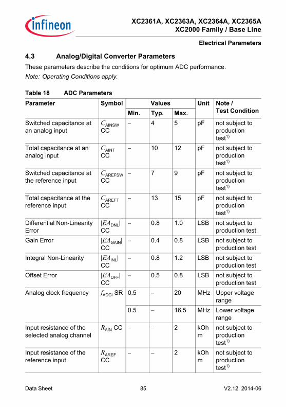
XC2361A, XC2363A, XC2364A, XC2365AXC2000 Family / Base Line
Electrical Parameters
Data Sheet 85 V2.12, 2014-06
4.3 Analog/Digital Converter ParametersThese parameters describe the conditions for optimum ADC performance.Note: Operating Conditions apply.
Table 18 ADC ParametersParameter Symbol Values Unit Note /
Test ConditionMin. Typ. Max.Switched capacitance at an analog input
CAINSW CC
− 4 5 pF not subject to production test1)
Total capacitance at an analog input
CAINT CC
− 10 12 pF not subject to production test1)
Switched capacitance at the reference input
CAREFSW CC
− 7 9 pF not subject to production test1)
Total capacitance at the reference input
CAREFT CC
− 13 15 pF not subject to production test1)
Differential Non-Linearity Error
|EADNL| CC
− 0.8 1.0 LSB not subject to production test
Gain Error |EAGAIN| CC
− 0.4 0.8 LSB not subject to production test
Integral Non-Linearity |EAINL| CC
− 0.8 1.2 LSB not subject to production test
Offset Error |EAOFF| CC
− 0.5 0.8 LSB not subject to production test
Analog clock frequency fADCI SR 0.5 − 20 MHz Upper voltage range
0.5 − 16.5 MHz Lower voltage range
Input resistance of the selected analog channel
RAIN CC − − 2 kOhm
not subject to production test1)
Input resistance of the reference input
RAREF CC
− − 2 kOhm
not subject to production test1)

XC2361A, XC2363A, XC2364A, XC2365AXC2000 Family / Base Line
Electrical Parameters
Data Sheet 86 V2.12, 2014-06
Broken wire detection delay against VAGND2)
tBWG CC − − 50 3)
Broken wire detection delay against VAREF2)
tBWR CC − − 50 4)
Conversion time for 8-bit result2)
tc8 CC (11 + STC) x tADCI+ 2 x tSYS
Conversion time for 10-bit result2)
tc10 CC (13 + STC) x tADCI+ 2 x tSYS
Total Unadjusted Error |TUE| CC
− 1 2 LSB 5)
Wakeup time from analog powerdown, fast mode2)
tWAF CC − − 4 μs
Wakeup time from analog powerdown, slow mode2)
tWAS CC − − 15 μs
Analog reference ground VAGND SR
VSS- 0.05
− 1.5 V
Analog input voltage range
VAIN SR VAGND − VAREF V 6)
Analog reference voltage VAREF SR
VAGND+ 1.0
− VDDPA+ 0.05
V 5)
1) These parameter values cover the complete operating range. Under relaxed operating conditions (roomtemperature, nominal supply voltage) the typical values can be used for calculation.
2) This parameter includes the sample time (also the additional sample time specified by STC), the time todetermine the digital result and the time to load the result register with the conversion result. Values for thebasic clock tADCI depend on programming.
3) The broken wire detection delay against VAGND is measured in numbers of consecutive precharge cycles at aconversion rate of not more than 500 µs. Result below 10% (66H).
4) The broken wire detection delay against VAREF is measured in numbers of consecutive precharge cycles at aconversion rate of not more than 10 µs. This function is influenced by leakage current, in particular at hightemperature. Result above 80% (332H).
5) TUE is tested at VAREF = VDDPA = 5.0 V, VAGND = 0 V. It is verified by design for all other voltages within thedefined voltage range. The specified TUE is valid only if the absolute sum of input overload currents on analogport pins (see IOV specification) does not exceed 10 mA, and if VAREF and VAGND remain stable during themeasurement time.
6) VAIN may exceed VAGND or VAREF up to the absolute maximum ratings. However, the conversion result in thesecases will be X000H or X3FFH, respectively.
Table 18 ADC Parameters (cont’d)Parameter Symbol Values Unit Note /
Test ConditionMin. Typ. Max.

XC2361A, XC2363A, XC2364A, XC2365AXC2000 Family / Base Line
Electrical Parameters
Data Sheet 87 V2.12, 2014-06
Figure 16 Equivalent Circuitry for Analog Inputs
A/D Converter
MCS05570
RSource
VAIN CExt CAINT CAINS-
RAIN, On
CAINS

XC2361A, XC2363A, XC2364A, XC2365AXC2000 Family / Base Line
Electrical Parameters
Data Sheet 88 V2.12, 2014-06
Sample time and conversion time of the XC236xA’s A/D converters are programmable.The timing above can be calculated using Table 19.The limit values for fADCI must not be exceeded when selecting the prescaler value.
Converter Timing Example A:
Converter Timing Example B:
Table 19 A/D Converter Computation TableGLOBCTR.5-0(DIVA)
A/D ConverterAnalog Clock fADCI
INPCRx.7-0(STC)
Sample Time1)
tS
1) The selected sample time is doubled if broken wire detection is active (due to the presampling phase).
000000B fSYS 00H tADCI × 2000001B fSYS / 2 01H tADCI × 3000010B fSYS / 3 02H tADCI × 4: fSYS / (DIVA+1) : tADCI × (STC+2)111110B fSYS / 63 FEH tADCI × 256111111B fSYS / 64 FFH tADCI × 257
Assumptions: fSYS = 80 MHz (i.e. tSYS = 12.5 ns), DIVA = 03H, STC = 00H
Analog clock fADCI = fSYS / 4 = 20 MHz, i.e. tADCI = 50 nsSample time tS = tADCI × 2 = 100 nsConversion 10-bit:
tC10 = 13 × tADCI + 2 × tSYS = 13 × 50 ns + 2 × 12.5 ns = 0.675 μsConversion 8-bit:
tC8 = 11 × tADCI + 2 × tSYS = 11 × 50 ns + 2 × 12.5 ns = 0.575 μs
Assumptions: fSYS = 40 MHz (i.e. tSYS = 25 ns), DIVA = 02H, STC = 03H
Analog clock fADCI = fSYS / 3 = 13.3 MHz, i.e. tADCI = 75 nsSample time tS = tADCI × 5 = 375 nsConversion 10-bit:
tC10 = 16 × tADCI + 2 × tSYS = 16 × 75 ns + 2 × 25 ns = 1.25 μsConversion 8-bit:
tC8 = 14 × tADCI + 2 × tSYS = 14 × 75 ns + 2 × 25 ns = 1.10 μs
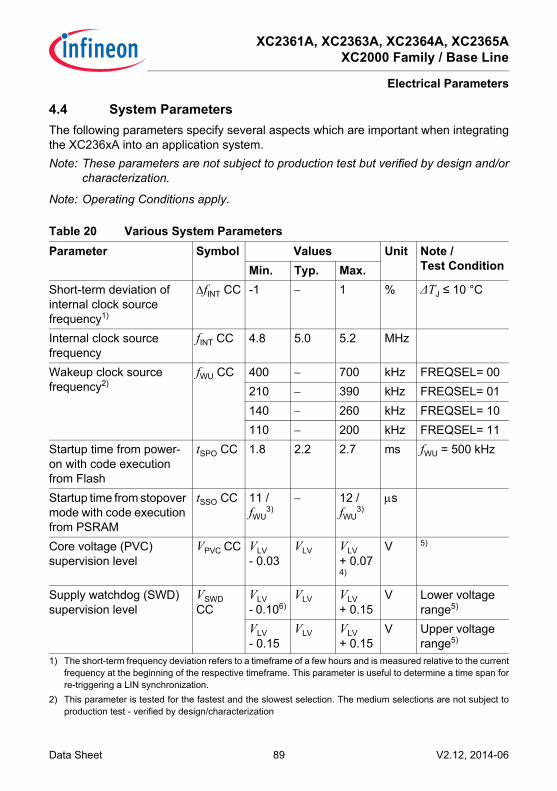
XC2361A, XC2363A, XC2364A, XC2365AXC2000 Family / Base Line
Electrical Parameters
Data Sheet 89 V2.12, 2014-06
4.4 System ParametersThe following parameters specify several aspects which are important when integratingthe XC236xA into an application system.Note: These parameters are not subject to production test but verified by design and/or
characterization.
Note: Operating Conditions apply.
Table 20 Various System ParametersParameter Symbol Values Unit Note /
Test ConditionMin. Typ. Max.Short-term deviation of internal clock source frequency1)
1) The short-term frequency deviation refers to a timeframe of a few hours and is measured relative to the currentfrequency at the beginning of the respective timeframe. This parameter is useful to determine a time span forre-triggering a LIN synchronization.
ΔfINT CC -1 − 1 % ΔTJ ≤ 10 °C
Internal clock source frequency
fINT CC 4.8 5.0 5.2 MHz
Wakeup clock source frequency2)
2) This parameter is tested for the fastest and the slowest selection. The medium selections are not subject toproduction test - verified by design/characterization
fWU CC 400 − 700 kHz FREQSEL= 00210 − 390 kHz FREQSEL= 01140 − 260 kHz FREQSEL= 10110 − 200 kHz FREQSEL= 11
Startup time from power-on with code execution from Flash
tSPO CC 1.8 2.2 2.7 ms fWU = 500 kHz
Startup time from stopover mode with code execution from PSRAM
tSSO CC 11 /fWU
3)− 12 /
fWU3)
μs
Core voltage (PVC) supervision level
VPVC CC VLV- 0.03
VLV VLV+ 0.07 4)
V 5)
Supply watchdog (SWD) supervision level
VSWD CC
VLV- 0.106)
VLV VLV+ 0.15
V Lower voltage range5)
VLV- 0.15
VLV VLV+ 0.15
V Upper voltage range5)
XC2361A, XC2363A, XC2364A, XC2365AXC2000 Family / Base Line
Electrical Parameters
Data Sheet 90 V2.12, 2014-06
Conditions for tSPO Timing MeasurementThe time required for the transition from Power-On to Base mode is called tSPO. It ismeasured under the following conditions:Precondition: The pad supply is valid, i.e. VDDPB is above 3.0 V and remains above 3.0 Veven though the XC236xA is starting up. No debugger is attached.Start condition: Power-on reset is removed (PORST = 1).End condition: External pin toggle caused by first user instruction executed from FLASHafter startup.
Conditions for tSSO Timing MeasurementThe time required for the transition from Stopover to Stopover Waked-Up mode iscalled tSSO. It is measured under the following conditions:Precondition: The Stopover mode has been entered using the procedure defined in theProgrammer’s Guide.Start condition: Pin toggle on ESR pin triggering the startup sequence.End condition: External pin toggle caused by first user instruction executed from PSRAMafter startup.
Coding of bit fields LEVxV in SWD and PVC Configuration Registers
3) fWU in MHz4) This value includes a hysteresis of approximately 50 mV for rising voltage.5) VLV = selected SWD voltage level6) The limit VLV - 0.10 V is valid for the OK1 level. The limit for the OK2 level is VLV - 0.15 V.
Table 21 Coding of bit fields LEVxV in Register SWDCON0Code Default Voltage Level Notes1)
0000B 2.9 V0001B 3.0 V LEV1V: reset request0010B 3.1 V0011B 3.2 V0100B 3.3 V0101B 3.4 V0110B 3.6 V0111B 4.0 V1000B 4.2 V
XC2361A, XC2363A, XC2364A, XC2365AXC2000 Family / Base Line
Electrical Parameters
Data Sheet 91 V2.12, 2014-06
1001B 4.5 V LEV2V: no request1010B 4.6 V1011B 4.7 V1100B 4.8 V1101B 4.9 V1110B 5.0 V1111B 5.5 V1) The indicated default levels are selected automatically after a power reset.
Table 22 Coding of Bitfields LEVxV in Registers PVCyCONzCode Default Voltage Level Notes1)
1) The indicated default levels are selected automatically after a power reset.
000B 0.95 V001B 1.05 V010B 1.15 V011B 1.25 V100B 1.35 V LEV1V: reset request101B 1.45 V LEV2V: interrupt request2)
2) Due to variations of the tolerance of both the Embedded Voltage Regulators (EVR) and the PVC levels, thisinterrupt can be triggered inadvertently, even though the core voltage is within the normal range. It is,therefore, recommended not to use the this warning level.
110B 1.55 V111B 1.65 V
Table 21 Coding of bit fields LEVxV in Register SWDCON0 (cont’d)Code Default Voltage Level Notes1)
XC2361A, XC2363A, XC2364A, XC2365AXC2000 Family / Base Line
Electrical Parameters
Data Sheet 92 V2.12, 2014-06
4.5 Flash Memory ParametersThe XC236xA is delivered with all Flash sectors erased and with no protection installed.The data retention time of the XC236xA’s Flash memory (i.e. the time after which storeddata can still be retrieved) depends on the number of times the Flash memory has beenerased and programmed.Note: These parameters are not subject to production test but verified by design and/or
characterization.
Note: Operating Conditions apply.
Table 23 Flash ParametersParameter Symbol Values Unit Note /
Test ConditionMin. Typ. Max.Parallel Flash module program/erase limit depending on Flash read activity
NPP SR − − 41) NFL_RD ≤ 1,fSYS ≤ 80 MHz
− − 12) NFL_RD > 1
Flash erase endurance for security pages
NSEC SR 10 − − cycles
tRET ≥ 20 years
Flash wait states3) NWSFLAS
H SR1 − − fSYS ≤ 8 MHz2 − − fSYS ≤ 13 MHz3 − − fSYS ≤ 17 MHz4 − − fSYS > 17 MHz
Erase time per sector/page
tER CC − 74) 8.0 ms
Programming time per page
tPR CC − 34) 3.5 ms
Data retention time tRET CC 20 − − years
NEr ≤ 1 000 cycles
Drain disturb limit NDD SR 32 − − cycles

XC2361A, XC2363A, XC2364A, XC2365AXC2000 Family / Base Line
Electrical Parameters
Data Sheet 93 V2.12, 2014-06
Access to the XC236xA Flash modules is controlled by the IMB. Built-in prefetchmechanisms optimize the performance for sequential access.Flash access waitstates only affect non-sequential access. Due to prefetchmechanisms, the performance for sequential access (depending on the softwarestructure) is only partially influenced by waitstates.
Number of erase cycles NEr SR − − 15 000 cycles
tRET ≥ 5 years;Valid for up to 64 user-selected sectors (data storage)
− − 1 000 cycles
tRET ≥ 20 years
1) All Flash module(s) can be erased/programmed while code is executed and/or data is read from only oneFlash module or from PSRAM. The Flash module that delivers code/data can, of course, not beerased/programmed.
2) Flash module 3 can be erased/programmed while code is executed and/or data is read from any other Flashmodule.
3) Value of IMB_IMBCTRL.WSFLASH.4) Programming and erase times depend on the internal Flash clock source. The control state machine needs a
few system clock cycles. This increases the stated durations noticably only at extremely low system clockfrequencies.
Table 23 Flash Parameters (cont’d)Parameter Symbol Values Unit Note /
Test ConditionMin. Typ. Max.
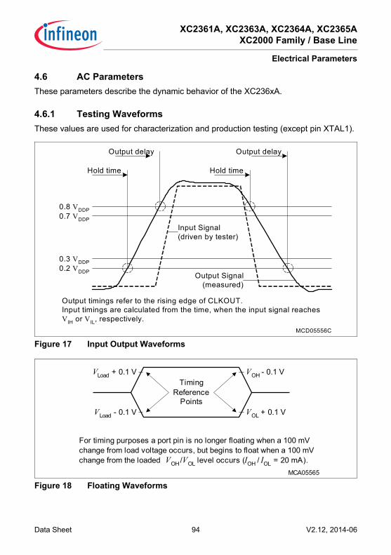
XC2361A, XC2363A, XC2364A, XC2365AXC2000 Family / Base Line
Electrical Parameters
Data Sheet 94 V2.12, 2014-06
4.6 AC ParametersThese parameters describe the dynamic behavior of the XC236xA.
4.6.1 Testing WaveformsThese values are used for characterization and production testing (except pin XTAL1).
Figure 17 Input Output Waveforms
Figure 18 Floating Waveforms
MCD05556C
0.3 VDDP
Input Signal(driven by tester)
Output Signal(measured)
Hold time
Output delay Output delay
Hold time
Output timings refer to the rising edge of CLKOUT.Input timings are calculated from the time, when the input signal reachesVIH or VIL, respectively.
0.2 VDDP
0.8 VDDP0.7 VDDP
MCA05565
TimingReference
Points
VLoad + 0.1 V
VLoad - 0.1 V
VOH - 0.1 V
VOL + 0.1 V
For timing purposes a port pin is no longer floating when a 100 mVchange from load voltage occurs, but begins to float when a 100 mVchange from the loaded VOH /VOL level occurs (IOH / IOL = 20 mA).

XC2361A, XC2363A, XC2364A, XC2365AXC2000 Family / Base Line
Electrical Parameters
Data Sheet 95 V2.12, 2014-06
4.6.2 Definition of Internal TimingThe internal operation of the XC236xA is controlled by the internal system clock fSYS.Because the system clock signal fSYS can be generated from a number of internal andexternal sources using different mechanisms, the duration of the system clock periods(TCSs) and their variation (as well as the derived external timing) depend on themechanism used to generate fSYS. This must be considered when calculating the timingfor the XC236xA.
Figure 19 Generation Mechanisms for the System Clock
Note: The example of PLL operation shown in Figure 19 uses a PLL factor of 1:4; theexample of prescaler operation uses a divider factor of 2:1.
The specification of the external timing (AC Characteristics) depends on the period of thesystem clock (TCS).
MC_XC2X_CLOCKGEN
Phase Locked Loop Operation (1:N)
fIN
Direct Clock Drive (1:1)
Prescaler Operation (N:1)
fSYS
fIN
fSYS
fIN
fSYS
TCS
TCS
TCS

XC2361A, XC2363A, XC2364A, XC2365AXC2000 Family / Base Line
Electrical Parameters
Data Sheet 96 V2.12, 2014-06
Direct DriveWhen direct drive operation is selected (SYSCON0.CLKSEL = 11B), the system clock isderived directly from the input clock signal CLKIN1:fSYS = fIN.The frequency of fSYS is the same as the frequency of fIN. In this case the high and lowtimes of fSYS are determined by the duty cycle of the input clock fIN.Selecting Bypass Operation from the XTAL11) input and using a divider factor of 1 resultsin a similar configuration.
Prescaler OperationWhen prescaler operation is selected (SYSCON0.CLKSEL = 10B, PLLCON0.VCOBY =1B), the system clock is derived either from the crystal oscillator (input clock signalXTAL1) or from the internal clock source through the output prescaler K1 (= K1DIV+1):fSYS = fOSC / K1.If a divider factor of 1 is selected, the frequency of fSYS equals the frequency of fOSC. Inthis case the high and low times of fSYS are determined by the duty cycle of the inputclock fOSC (external or internal).The lowest system clock frequency results from selecting the maximum value for thedivider factor K1:fSYS = fOSC / 1024.
4.6.2.1 Phase Locked Loop (PLL)When PLL operation is selected (SYSCON0.CLKSEL = 10B, PLLCON0.VCOBY = 0B),the on-chip phase locked loop is enabled and provides the system clock. The PLLmultiplies the input frequency by the factor F (fSYS = fIN × F).F is calculated from the input divider P (= PDIV+1), the multiplication factor N (=NDIV+1), and the output divider K2 (= K2DIV+1):(F = N / (P × K2)).The input clock can be derived either from an external source at XTAL1 or from the on-chip clock source.The PLL circuit synchronizes the system clock to the input clock. This synchronization isperformed smoothly so that the system clock frequency does not change abruptly.Adjustment to the input clock continuously changes the frequency of fSYS so that it islocked to fIN. The slight variation causes a jitter of fSYS which in turn affects the durationof individual TCSs.
1) Voltages on XTAL1 must comply to the core supply voltage VDDIM.

XC2361A, XC2363A, XC2364A, XC2365AXC2000 Family / Base Line
Electrical Parameters
Data Sheet 97 V2.12, 2014-06
The timing in the AC Characteristics refers to TCSs. Timing must be calculated using theminimum TCS possible under the given circumstances.The actual minimum value for TCS depends on the jitter of the PLL. Because the PLL isconstantly adjusting its output frequency to correspond to the input frequency (fromcrystal or oscillator), the accumulated jitter is limited. This means that the relativedeviation for periods of more than one TCS is lower than for a single TCS (see formulasand Figure 20).This is especially important for bus cycles using waitstates and for the operation oftimers, serial interfaces, etc. For all slower operations and longer periods (e.g. pulse traingeneration or measurement, lower baudrates, etc.) the deviation caused by the PLL jitteris negligible.The value of the accumulated PLL jitter depends on the number of consecutive VCOoutput cycles within the respective timeframe. The VCO output clock is divided by theoutput prescaler K2 to generate the system clock signal fSYS. The number of VCO cyclesis K2 × T, where T is the number of consecutive fSYS cycles (TCS).The maximum accumulated jitter (long-term jitter) DTmax is defined by:DTmax [ns] = ±(220 / (K2 × fSYS) + 4.3)This maximum value is applicable, if either the number of clock cycles T > (fSYS / 1.2) orthe prescaler value K2 > 17.In all other cases for a timeframe of T × TCS the accumulated jitter DT is determined by:DT [ns] = DTmax × [(1 - 0.058 × K2) × (T - 1) / (0.83 × fSYS - 1) + 0.058 × K2]fSYS in [MHz] in all formulas.Example, for a period of 3 TCSs @ 33 MHz and K2 = 4:Dmax = ±(220 / (4 × 33) + 4.3) = 5.97 ns (Not applicable directly in this case!)D3 = 5.97 × [(1 - 0.058 × 4) × (3 - 1) / (0.83 × 33 - 1) + 0.058 × 4]= 5.97 × [0.768 × 2 / 26.39 + 0.232]= 1.7 nsExample, for a period of 3 TCSs @ 33 MHz and K2 = 2:Dmax = ±(220 / (2 × 33) + 4.3) = 7.63 ns (Not applicable directly in this case!)D3 = 7.63 × [(1 - 0.058 × 2) × (3 - 1) / (0.83 × 33 - 1) + 0.058 × 2]= 7.63 × [0.884 × 2 / 26.39 + 0.116]= 1.4 ns

XC2361A, XC2363A, XC2364A, XC2365AXC2000 Family / Base Line
Electrical Parameters
Data Sheet 98 V2.12, 2014-06
Figure 20 Approximated Accumulated PLL Jitter
Note: The specified PLL jitter values are valid if the capacitive load per pin does notexceed CL = 20 pF.The maximum peak-to-peak noise on the pad supply voltage (measured betweenVDDPB pin 100 and VSS pin 1) is limited to a peak-to-peak voltage of VPP = 50 mV.This can be achieved by appropriate blocking of the supply voltage as close aspossible to the supply pins and using PCB supply and ground planes.
MC_XC2X_JITTER
Cycles T0
±1
±2
±3
±4
±5
±6
±7
±8
Acc. jitter DT
20 40 60 80 100
nsfSYS = 66 MHz
1
fVCO = 132 MHz
fVCO = 66 MHz
±9fSYS = 33 MHz

XC2361A, XC2363A, XC2364A, XC2365AXC2000 Family / Base Line
Electrical Parameters
Data Sheet 99 V2.12, 2014-06
PLL frequency band selectionDifferent frequency bands can be selected for the VCO so that the operation of the PLLcan be adjusted to a wide range of input and output frequencies:
4.6.2.2 Wakeup ClockWhen wakeup operation is selected (SYSCON0.CLKSEL = 00B), the system clock isderived from the low-frequency wakeup clock source:fSYS = fWU.In this mode, a basic functionality can be maintained without requiring an external clocksource and while minimizing the power consumption.
4.6.2.3 Selecting and Changing the Operating FrequencyWhen selecting a clock source and the clock generation method, the requiredparameters must be carefully written to the respective bit fields, to avoid unintendedintermediate states.Many applications change the frequency of the system clock (fSYS) during operation inorder to optimize system performance and power consumption. Changing the operatingfrequency also changes the switching currents, which influences the power supply.To ensure proper operation of the on-chip EVRs while they generate the core voltage,the operating frequency shall only be changed in certain steps. This prevents overshootsand undershoots of the supply voltage.To avoid the indicated problems, recommended sequences are provided which ensurethe intended operation of the clock system interacting with the power system.Please refer to the Programmer’s Guide.
Table 24 System PLL ParametersParameter Symbol Values Unit Note /
Test ConditionMin. Typ. Max.VCO output frequency(VCO controlled)
fVCO CC 50 − 110 MHz VCOSEL = 00B
100 − 160 MHz VCOSEL = 01B
VCO output frequency(VCO free-running)
fVCO CC 10 − 40 MHz VCOSEL = 00B
20 − 80 MHz VCOSEL = 01B

XC2361A, XC2363A, XC2364A, XC2365AXC2000 Family / Base Line
Electrical Parameters
Data Sheet 100 V2.12, 2014-06
4.6.3 External Clock Input ParametersThese parameters specify the external clock generation for the XC236xA. The clock canbe generated in two ways:• By connecting a crystal or ceramic resonator to pins XTAL1/XTAL2• By supplying an external clock signal
– This clock signal can be supplied either to pin XTAL1 (core voltage domain) or topin CLKIN1 (IO voltage domain)
If connected to CLKIN1, the input signal must reach the defined input levels VIL and VIH.If connected to XTAL1, a minimum amplitude VAX1 (peak-to-peak voltage) is sufficient forthe operation of the on-chip oscillator.Note: The given clock timing parameters (t1 … t4) are only valid for an external clock
input signal.
Note: Operating Conditions apply.
Table 25 External Clock Input CharacteristicsParameter Symbol Values Unit Note /
Test ConditionMin. Typ. Max.Oscillator frequency fOSC SR 4 − 40 MHz Input = clock
signal4 − 16 MHz Input = crystal
or ceramic resonator
XTAL1 input current absolute value
|IIL| CC − − 20 μA
Input clock high time t1 SR 6 − − nsInput clock low time t2 SR 6 − − nsInput clock rise time t3 SR − − 8 nsInput clock fall time t4 SR − − 8 nsInput voltage amplitude on XTAL11)
VAX1 SR 0.3 x VDDIM
− − V 4 to 16 MHz
0.4 x VDDIM
− − V 16 to 25 MHz
0.5 x VDDIM
− − V 25 to 40 MHz
Input voltage range limits for signal on XTAL1
VIX1 SR -1.7 + VDDIM
− 1.7 V 2)
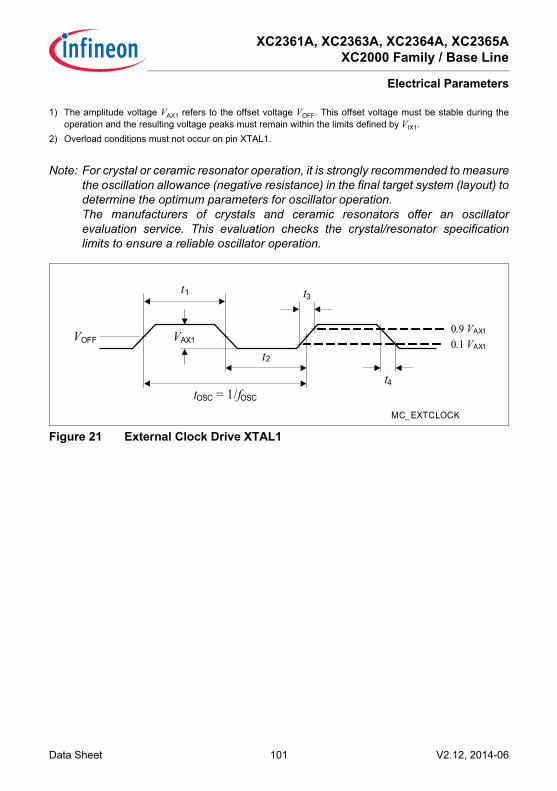
XC2361A, XC2363A, XC2364A, XC2365AXC2000 Family / Base Line
Electrical Parameters
Data Sheet 101 V2.12, 2014-06
Note: For crystal or ceramic resonator operation, it is strongly recommended to measurethe oscillation allowance (negative resistance) in the final target system (layout) todetermine the optimum parameters for oscillator operation.The manufacturers of crystals and ceramic resonators offer an oscillatorevaluation service. This evaluation checks the crystal/resonator specificationlimits to ensure a reliable oscillator operation.
Figure 21 External Clock Drive XTAL1
1) The amplitude voltage VAX1 refers to the offset voltage VOFF. This offset voltage must be stable during theoperation and the resulting voltage peaks must remain within the limits defined by VIX1.
2) Overload conditions must not occur on pin XTAL1.
MC_EXTCLOCK
t1
t2
tOSC = 1/fOSC
t3
t4
VOFF VAX1 0.1 VAX1
0.9 VAX1

XC2361A, XC2363A, XC2364A, XC2365AXC2000 Family / Base Line
Electrical Parameters
Data Sheet 102 V2.12, 2014-06
4.6.4 Pad PropertiesThe output pad drivers of the XC236xA can operate in several user-selectable modes.Strong driver mode allows controlling external components requiring higher currentssuch as power bridges or LEDs. Reducing the driving power of an output pad reduceselectromagnetic emissions (EME). In strong driver mode, selecting a slower edgereduces EME.The dynamic behavior, i.e. the rise time and fall time, depends on the applied externalcapacitance that must be charged and discharged. Timing values are given for acapacitance of 20 pF, unless otherwise noted.In general, the performance of a pad driver depends on the available supply voltageVDDP. The following table lists the pad parameters.Note: These parameters are not subject to production test but verified by design and/or
characterization.
Note: Operating Conditions apply.

XC2361A, XC2363A, XC2364A, XC2365AXC2000 Family / Base Line
Electrical Parameters
Data Sheet 103 V2.12, 2014-06
Table 26 is valid under the following conditions:VDDP ≥ 4.5 V; VDDPtyp = 5 V; VDDP ≤ 5.5 V; CL ≥ 20 pF; CL ≤ 100 pF;
Table 26 Standard Pad Parameters for Upper Voltage RangeParameter Symbol Values Unit Note /
Test ConditionMin. Typ. Max.Maximum output driver current (absolute value)1)
1) The total output current that may be drawn at a given time must be limited to protect the supply rails fromdamage. For any group of 16 neighboring output pins, the total output current in each direction (ΣIOL and Σ-IOH) must remain below 50 mA.
IOmax CC
− − 10 mA Strong driver− − 4.0 mA Medium driver− − 0.5 mA Weak driver
Nominal output driver current (absolute value)
IOnom CC
− − 2.5 mA Strong driver− − 1.0 mA Medium driver− − 0.1 mA Weak driver
Rise and Fall times (10% - 90%)
tRF CC − − 4.2 + 0.14 x CL
ns Strong driver; Sharp edge
− − 11.6 + 0.22 x CL
ns Strong driver; Medium edge
− − 20.6 + 0.22 x CL
ns Strong driver; Slow edge
− − 23 + 0.6 x CL
ns Medium driver
− − 212 + 1.9 x CL
ns Weak driver

XC2361A, XC2363A, XC2364A, XC2365AXC2000 Family / Base Line
Electrical Parameters
Data Sheet 104 V2.12, 2014-06
Table 27 is valid under the following conditions:VDDP ≥ 3.0 V; VDDPtyp = 3.3 V; VDDP ≤ 4.5 V; CL ≥ 20 pF; CL ≤ 100 pF;
Table 27 Standard Pad Parameters for Lower Voltage RangeParameter Symbol Values Unit Note /
Test ConditionMin. Typ. Max.Maximum output driver current (absolute value)1)
1) The total output current that may be drawn at a given time must be limited to protect the supply rails fromdamage. For any group of 16 neighboring output pins, the total output current in each direction (ΣIOL and Σ-IOH) must remain below 50 mA.
IOmax CC
− − 10 mA Strong driver− − 2.5 mA Medium driver− − 0.5 mA Weak driver
Nominal output driver current (absolute value)
IOnom CC
− − 2.5 mA Strong driver− − 1.0 mA Medium driver− − 0.1 mA Weak driver
Rise and Fall times (10% - 90%)
tRF CC − − 6.2 + 0.24 x CL
ns Strong driver; Sharp edge
− − 24 + 0.3 x CL
ns Strong driver; Medium edge
− − 34 + 0.3 x CL
ns Strong driver; Slow edge
− − 37 + 0.65 x CL
ns Medium driver
− − 500 + 2.5 x CL
ns Weak driver

XC2361A, XC2363A, XC2364A, XC2365AXC2000 Family / Base Line
Electrical Parameters
Data Sheet 105 V2.12, 2014-06
4.6.5 External Bus TimingThe following parameters specify the behavior of the XC236xA bus interface.Note: These parameters are not subject to production test but verified by design and/or
characterization.
Note: Operating Conditions apply.
Bus Interface Performance LimitsThe output frequency at the bus interface pins is limited by the performance of the outputdrivers. The fast clock driver (used for CLKOUT) can drive 80-MHz signals, the standarddrivers can drive 40-MHz signalsTherefore, the speed of the EBC must be limited, either by limiting the system frequencyto fSYS ≤ 80 MHz or by adding waitstates so that signal transitions have a minimumdistance of 12.5 ns.For a description of the bus protocol and the programming of its variable timingparameters, please refer to the User’s Manual.
Figure 22 CLKOUT Signal Timing
Table 28 EBC ParametersParameter Symbol Values Unit Note /
Test ConditionMin. Typ. Max.CLKOUT Cycle Time1)
1) The CLKOUT cycle time is influenced by PLL jitter. For longer periods the relative deviation decreases (seePLL deviation formula).
t5 CC − 1 / fSYS − nsCLKOUT high time t6 CC 2 − −
CLKOUT low time t7 CC 2 − −
CLKOUT rise time t8 CC − − 3 nsCLKOUT fall time t9 CC − − 3
MC_X_EBCCLKOUT
CLKOUT
t5 t6 t7 t8t9

XC2361A, XC2363A, XC2364A, XC2365AXC2000 Family / Base Line
Electrical Parameters
Data Sheet 106 V2.12, 2014-06
Note: The term CLKOUT refers to the reference clock output signal which is generatedby selecting fSYS as the source signal for the clock output signal EXTCLK on pinP2.8 and by enabling the high-speed clock driver on this pin.
Variable Memory CyclesExternal bus cycles of the XC236xA are executed in five consecutive cycle phases (AB,C, D, E, F). The duration of each cycle phase is programmable (via the TCONCSxregisters) to adapt the external bus cycles to the respective external module (memory,peripheral, etc.).The duration of the access phase can optionally be controlled by the external moduleusing the READY handshake input.This table provides a summary of the phases and the ranges for their length.
Note: The bandwidth of a parameter (from minimum to maximum value) covers thewhole operating range (temperature, voltage) as well as process variations. Withina given device, however, this bandwidth is smaller than the specified range. Thisis also due to interdependencies between certain parameters. Some of theseinterdependencies are described in additional notes (see standard timing).
Note: Operating Conditions apply; CL = 20 pF.
Table 29 Programmable Bus Cycle Phases (see timing diagrams)Bus Cycle Phase Parameter Valid Values UnitAddress setup phase, the standard duration of this phase (1 … 2 TCS) can be extended by 0 … 3 TCS if the address window is changed
tpAB 1 … 2 (5) TCS
Command delay phase tpC 0 … 3 TCSWrite Data setup/MUX Tristate phase tpD 0 … 1 TCSAccess phase tpE 1 … 32 TCSAddress/Write Data hold phase tpF 0 … 3 TCS

XC2361A, XC2363A, XC2364A, XC2365AXC2000 Family / Base Line
Electrical Parameters
Data Sheet 107 V2.12, 2014-06
Table 30 EBC External Bus Timing for Upper Voltage RangeParameter Symbol Values Unit Note /
Test ConditionMin. Typ. Max.Output valid delay for RD, WR(L/H)
t10 CC − 7 13 ns
Output valid delay for BHE, ALE
t11 CC − 7 14 ns
Address output valid delay for A23 ... A0
t12 CC − 8 14 ns
Address output valid delay for AD15 ... AD0 (MUX mode)
t13 CC − 8 15 ns
Output valid delay for CS t14 CC − 7 13 nsData output valid delay for AD15 ... AD0 (write data, MUX mode)
t15 CC − 8 15 ns
Data output valid delay for D15 ... D0 (write data, DEMUX mode)
t16 CC − 8 15 ns
Output hold time for RD, WR(L/H)
t20 CC -2 6 8 ns
Output hold time for BHE, ALE
t21 CC -2 6 10 ns
Address output hold time for AD15 ... AD0
t23 CC -3 6 8 ns
Output hold time for CS t24 CC -3 6 11 nsData output hold time for D15 ... D0 and AD15 ... AD0
t25 CC -3 6 8 ns
Input setup time for READY, D15 ... D0, AD15 ... AD0
t30 SR 25 15 − ns
Input hold time READY, D15 ... D0, AD15 ... AD01)
1) Read data are latched with the same internal clock edge that triggers the address change and the rising edgeof RD. Address changes before the end of RD have no impact on (demultiplexed) read cycles. Read data canchange after the rising edge of RD.
t31 SR 0 -7 − ns

XC2361A, XC2363A, XC2364A, XC2365AXC2000 Family / Base Line
Electrical Parameters
Data Sheet 108 V2.12, 2014-06
Table 31 EBC External Bus Timing for Lower Voltage RangeParameter Symbol Values Unit Note /
Test ConditionMin. Typ. Max.Output valid delay for RD, WR(L/H)
t10 CC − 11 20 ns
Output valid delay for BHE, ALE
t11 CC − 10 21 ns
Address output valid delay for A23 ... A0
t12 CC − 11 22 ns
Address output valid delay for AD15 ... AD0 (MUX mode)
t13 CC − 10 22 ns
Output valid delay for CS t14 CC − 10 13 nsData output valid delay for AD15 ... AD0 (write data, MUX mode)
t15 CC − 10 22 ns
Data output valid delay for D15 ... D0 (write data, DEMUX mode)
t16 CC − 10 22 ns
Output hold time for RD, WR(L/H)
t20 CC -2 8 10 ns
Output hold time for BHE, ALE
t21 CC -2 8 10 ns
Address output hold time for AD15 ... AD0
t23 CC -3 8 10 ns
Output hold time for CS t24 CC -3 8 11 nsData output hold time for D15 ... D0 and AD15 ... AD0
t25 CC -3 8 10 ns
Input setup time for READY, D15 ... D0, AD15 ... AD0
t30 SR 29 17 − ns
Input hold time READY, D15 ... D0, AD15 ... AD01)
1) Read data are latched with the same internal clock edge that triggers the address change and the rising edgeof RD. Address changes before the end of RD have no impact on (demultiplexed) read cycles. Read data canchange after the rising edge of RD.
t31 SR 0 -9 − ns
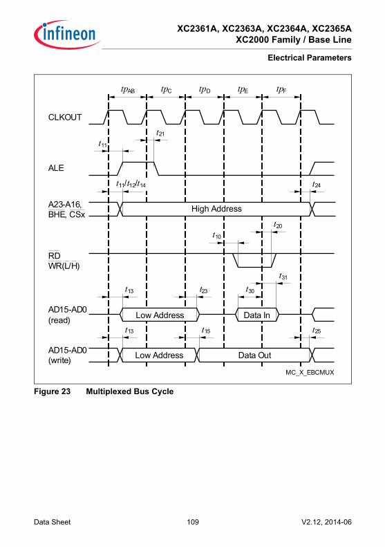
XC2361A, XC2363A, XC2364A, XC2365AXC2000 Family / Base Line
Electrical Parameters
Data Sheet 109 V2.12, 2014-06
Figure 23 Multiplexed Bus Cycle
CLKOUT
tpAB tpC tpD tpE tpF
ALE
t21
t11
A23-A16,BHE, CSx
t11/t12/t14
RDWR(L/H)
t20t10
Data InAD15-AD0(read)
t30
t31
MC_X_EBCMUX
AD15-AD0(write)
t13 t15 t25
t13 t23
Data OutLow Address
High Address
Low Address
t24

XC2361A, XC2363A, XC2364A, XC2365AXC2000 Family / Base Line
Electrical Parameters
Data Sheet 110 V2.12, 2014-06
Figure 24 Demultiplexed Bus Cycle
Address
tpAB tpC tpD tpE tpF
t21
t11
t11/t12/t14
t20t10
Data In
t30
t31
MC_X_EBCDEMUX
t16 t25
CLKOUT
ALE
A23-A0,BHE, CSx
RDWR(L/H)
D15-D0(read)
D15-D0(write) Data Out
t24

XC2361A, XC2363A, XC2364A, XC2365AXC2000 Family / Base Line
Electrical Parameters
Data Sheet 111 V2.12, 2014-06
4.6.5.1 Bus Cycle Control with the READY InputThe duration of an external bus cycle can be controlled by the external circuit using theREADY input signal. The polarity of this input signal can be selected.Synchronous READY permits the shortest possible bus cycle but requires the inputsignal to be synchronous to the reference signal CLKOUT.An asynchronous READY signal puts no timing constraints on the input signal but incursa minimum of one waitstate due to the additional synchronization stage. The minimumduration of an asynchronous READY signal for safe synchronization is one CLKOUTperiod plus the input setup time.An active READY signal can be deactivated in response to the trailing (rising) edge ofthe corresponding command (RD or WR).If the next bus cycle is controlled by READY, an active READY signal must be disabledbefore the first valid sample point in the next bus cycle. This sample point depends onthe programmed phases of the next cycle.
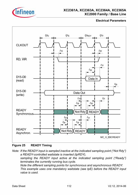
XC2361A, XC2363A, XC2364A, XC2365AXC2000 Family / Base Line
Electrical Parameters
Data Sheet 112 V2.12, 2014-06
Figure 25 READY Timing
Note: If the READY input is sampled inactive at the indicated sampling point (“Not Rdy”)a READY-controlled waitstate is inserted (tpRDY),sampling the READY input active at the indicated sampling point (“Ready”)terminates the currently running bus cycle.Note the different sampling points for synchronous and asynchronous READY.This example uses one mandatory waitstate (see tpE) before the READY inputvalue is used.
MC_X_EBCREADY
READYAsynchron.
Not Rdy READY
Data Out
t25
t30
D15-D0(write)
READYSynchronous Not Rdy READY
Data InD15-D0(read)
t10
RD, WR
tpD tpE tpRDY tpF
CLKOUT
t20
t30
t31
t31
t30
t31
t30
t31
t30
t31

XC2361A, XC2363A, XC2364A, XC2365AXC2000 Family / Base Line
Electrical Parameters
Data Sheet 113 V2.12, 2014-06
4.6.6 Synchronous Serial Interface TimingThe following parameters are applicable for a USIC channel operated in SSC mode.Note: These parameters are not subject to production test but verified by design and/or
characterization.
Note: Operating Conditions apply; CL = 20 pF.
Table 32 USIC SSC Master Mode Timing for Upper Voltage RangeParameter Symbol Values Unit Note /
Test ConditionMin. Typ. Max.Slave select output SELO active to first SCLKOUT transmit edge
t1 CC tSYS- 8 1)
1) tSYS = 1 / fSYS
− − ns
Slave select output SELO inactive after last SCLKOUT receive edge
t2 CC tSYS- 6 1)
− − ns
Data output DOUT valid time
t3 CC -6 − 9 ns
Receive data input setup time to SCLKOUT receive edge
t4 SR 31 − − ns
Data input DX0 hold time from SCLKOUT receive edge
t5 SR -4 − − ns
Table 33 USIC SSC Master Mode Timing for Lower Voltage RangeParameter Symbol Values Unit Note /
Test ConditionMin. Typ. Max.Slave select output SELO active to first SCLKOUT transmit edge
t1 CC tSYS- 10 1)
− − ns
Slave select output SELO inactive after last SCLKOUT receive edge
t2 CC tSYS- 9 1)
− − ns
Data output DOUT valid time
t3 CC -7 − 11 ns

XC2361A, XC2363A, XC2364A, XC2365AXC2000 Family / Base Line
Electrical Parameters
Data Sheet 114 V2.12, 2014-06
Receive data input setup time to SCLKOUT receive edge
t4 SR 40 − − ns
Data input DX0 hold time from SCLKOUT receive edge
t5 SR -5 − − ns
1) tSYS = 1 / fSYS
Table 34 USIC SSC Slave Mode Timing for Upper Voltage RangeParameter Symbol Values Unit Note /
Test ConditionMin. Typ. Max.Select input DX2 setup to first clock input DX1 transmit edge1)
1) These input timings are valid for asynchronous input signal handling of slave select input, shift clock input, andreceive data input (bits DXnCR.DSEN = 0).
t10 SR 7 − − ns
Select input DX2 hold after last clock input DX1 receive edge1)
t11 SR 7 − − ns
Receive data input setup time to shift clock receive edge1)
t12 SR 7 − − ns
Data input DX0 hold time from clock input DX1 receive edge1)
t13 SR 5 − − ns
Data output DOUT valid time
t14 CC 7 − 33 ns
Table 33 USIC SSC Master Mode Timing for Lower Voltage Range (cont’d)Parameter Symbol Values Unit Note /
Test ConditionMin. Typ. Max.

XC2361A, XC2363A, XC2364A, XC2365AXC2000 Family / Base Line
Electrical Parameters
Data Sheet 115 V2.12, 2014-06
Table 35 USIC SSC Slave Mode Timing for Lower Voltage RangeParameter Symbol Values Unit Note /
Test ConditionMin. Typ. Max.Select input DX2 setup to first clock input DX1 transmit edge1)
1) These input timings are valid for asynchronous input signal handling of slave select input, shift clock input, andreceive data input (bits DXnCR.DSEN = 0).
t10 SR 7 − − ns
Select input DX2 hold after last clock input DX1 receive edge1)
t11 SR 7 − − ns
Receive data input setup time to shift clock receive edge1)
t12 SR 7 − − ns
Data input DX0 hold time from clock input DX1 receive edge1)
t13 SR 5 − − ns
Data output DOUT valid time
t14 CC 8 − 41 ns

XC2361A, XC2363A, XC2364A, XC2365AXC2000 Family / Base Line
Electrical Parameters
Data Sheet 116 V2.12, 2014-06
Figure 26 USIC - SSC Master/Slave Mode Timing
Note: This timing diagram shows a standard configuration where the slave select signalis low-active and the serial clock signal is not shifted and not inverted.
t2t1
USIC_SSC_TMGX.VSD
Clock OutputSCLKOUT
Data OutputDOUT
t3 t3
t5Datavalid
t4
First Transmit Edge
Data InputDX0
Select OutputSELOx Active
Master Mode Timing
Slave Mode Timing
t11t10
Clock InputDX1
Data OutputDOUT
t14 t14
Datavalid
Data InputDX0
Select InputDX2
Active
t13
t12
Transmit Edge: with this clock edge, transmit data is shifted to transmit data output.Receive Edge: with this clock edge, receive data at receive data input is latched.
Receive Edge
Last Receive Edge
InactiveInactive
Transmit Edge
InactiveInactive
First Transmit Edge
Receive Edge
Transmit Edge
Last Receive Edge
t5Datavalid
t4
Datavalid
t12t13
Drawn for BRGH.SCLKCFG = 00B. Also valid for for SCLKCFG = 01B with inverted SCLKOUT signal.

XC2361A, XC2363A, XC2364A, XC2365AXC2000 Family / Base Line
Electrical Parameters
Data Sheet 117 V2.12, 2014-06
4.6.7 Debug Interface TimingThe debugger can communicate with the XC236xA either via the 2-pin DAP interface orvia the standard JTAG interface.
Debug via DAPThe following parameters are applicable for communication through the DAP debuginterface.Note: These parameters are not subject to production test but verified by design and/or
characterization.
Note: Operating Conditions apply; CL= 20 pF.
Table 36 DAP Interface Timing for Upper Voltage RangeParameter Symbol Values Unit Note /
Test ConditionMin. Typ. Max.DAP0 clock period t11 SR 251)
1) The debug interface cannot operate faster than the overall system, therefore t11 ≥ tSYS.
− − nsDAP0 high time t12 SR 8 − − nsDAP0 low time t13 SR 8 − − nsDAP0 clock rise time t14 SR − − 4 nsDAP0 clock fall time t15 SR − − 4 nsDAP1 setup to DAP0 rising edge
t16 SR 6 − − ns pad_type= standard
DAP1 hold after DAP0 rising edge
t17 SR 6 − − ns pad_type= standard
DAP1 valid per DAP0 clock period2)
2) The Host has to find a suitable sampling point by analyzing the sync telegram response.
t19 CC 17 20 − ns pad_type= standard

XC2361A, XC2363A, XC2364A, XC2365AXC2000 Family / Base Line
Electrical Parameters
Data Sheet 118 V2.12, 2014-06
Figure 27 Test Clock Timing (DAP0)
Table 37 DAP Interface Timing for Lower Voltage RangeParameter Symbol Values Unit Note /
Test ConditionMin. Typ. Max.DAP0 clock period t11 SR 251)
1) The debug interface cannot operate faster than the overall system, therefore t11 ≥ tSYS.
− − nsDAP0 high time t12 SR 8 − − nsDAP0 low time t13 SR 8 − − nsDAP0 clock rise time t14 SR − − 4 nsDAP0 clock fall time t15 SR − − 4 nsDAP1 setup to DAP0 rising edge
t16 SR 6 − − ns pad_type= standard
DAP1 hold after DAP0 rising edge
t17 SR 6 − − ns pad_type= standard
DAP1 valid per DAP0 clock period2)
2) The Host has to find a suitable sampling point by analyzing the sync telegram response.
t19 CC 12 17 − ns pad_type= standard
MC_DAP0
0.9 VDDP0.5 VDDP
t11
t12 t13
0.1 VDDPt15 t14

XC2361A, XC2363A, XC2364A, XC2365AXC2000 Family / Base Line
Electrical Parameters
Data Sheet 119 V2.12, 2014-06
Figure 28 DAP Timing Host to Device
Figure 29 DAP Timing Device to Host
Note: The transmission timing is determined by the receiving debugger by evaluating thesync-request synchronization pattern telegram.
t16 t17
DAP0
DAP1
MC_DAP1_RX
DAP1
MC_DAP1_TX
t11
t19

XC2361A, XC2363A, XC2364A, XC2365AXC2000 Family / Base Line
Electrical Parameters
Data Sheet 120 V2.12, 2014-06
Debug via JTAGThe following parameters are applicable for communication through the JTAG debuginterface. The JTAG module is fully compliant with IEEE1149.1-2000.Note: These parameters are not subject to production test but verified by design and/or
characterization.
Note: Operating Conditions apply; CL= 20 pF.
Table 38 JTAG Interface Timing for Upper Voltage RangeParameter Symbol Values Unit Note /
Test ConditionMin. Typ. Max.TCK clock period t1 SR 501)
1) The debug interface cannot operate faster than the overall system, therefore t1 ≥ tSYS.
− − ns 2)
2) Under typical conditions, the interface can operate at transfer rates up to 20 MHz.
TCK high time t2 SR 16 − − nsTCK low time t3 SR 16 − − nsTCK clock rise time t4 SR − − 8 nsTCK clock fall time t5 SR − − 8 nsTDI/TMS setup to TCK rising edge
t6 SR 6 − − ns
TDI/TMS hold after TCK rising edge
t7 SR 6 − − ns
TDO valid from TCK falling edge (propagation delay)3)
3) The falling edge on TCK is used to generate the TDO timing.
t8 CC − 25 29 ns
TDO high impedance to valid output from TCK falling edge4)3)
4) The setup time for TDO is given implicitly by the TCK cycle time.
t9 CC − 25 29 ns
TDO valid output to high impedance from TCK falling edge3)
t10 CC − 25 29 ns
TDO hold after TCK falling edge3)
t18 CC 5 − − ns

XC2361A, XC2363A, XC2364A, XC2365AXC2000 Family / Base Line
Electrical Parameters
Data Sheet 121 V2.12, 2014-06
Table 39 JTAG Interface Timing for Lower Voltage RangeParameter Symbol Values Unit Note /
Test ConditionMin. Typ. Max.TCK clock period t1 SR 501)
1) The debug interface cannot operate faster than the overall system, therefore t1 ≥ tSYS.
− − ns 2)
2) Under typical conditions, the interface can operate at transfer rates up to 20 MHz.
TCK high time t2 SR 16 − − nsTCK low time t3 SR 16 − − nsTCK clock rise time t4 SR − − 8 nsTCK clock fall time t5 SR − − 8 nsTDI/TMS setup to TCK rising edge
t6 SR 6 − − ns
TDI/TMS hold after TCK rising edge
t7 SR 6 − − ns
TDO valid from TCK falling edge (propagation delay)3)
3) The falling edge on TCK is used to generate the TDO timing.
t8 CC − 32 36 ns
TDO high impedance to valid output from TCK falling edge4)3)
4) The setup time for TDO is given implicitly by the TCK cycle time.
t9 CC − 32 36 ns
TDO valid output to high impedance from TCK falling edge3)
t10 CC − 32 36 ns
TDO hold after TCK falling edge3)
t18 CC 5 − − ns

XC2361A, XC2363A, XC2364A, XC2365AXC2000 Family / Base Line
Electrical Parameters
Data Sheet 122 V2.12, 2014-06
Figure 30 Test Clock Timing (TCK)
Figure 31 JTAG Timing
MC_JTAG_TCK
0.9 VDDP0.5 VDDP
t1
t2 t3
0.1 VDDPt5 t4
t6 t7
t6 t7
t9 t8 t10
TCK
TMS
TDI
TDO
MC_JTAG

XC2361A, XC2363A, XC2364A, XC2365AXC2000 Family / Base Line
Package and Reliability
Data Sheet 123 V2.12, 2014-06
5 Package and ReliabilityThe XC2000 Family devices use the package type PG-LQFP (Plastic Green - LowProfile Quad Flat Package). The following specifications must be regarded to ensureproper integration of the XC236xA in its target environment.
5.1 PackagingThese parameters specify the packaging rather than the silicon.
Note: To improve the EMC behavior, it is recommended to connect the exposed pad tothe board ground, independent of the thermal requirements.Board layout examples are given in an application note.
Package Compatibility ConsiderationsThe XC236xA is a member of the XC2000 Family of microcontrollers. It is alsocompatible to a certain extent with members of similar families or subfamilies.Each package is optimized for the device it houses. Therefore, there may be slightdifferences between packages of the same pin-count but for different device types. Inparticular, the size of the Exposed Pad (if present) may vary.If different device types are considered or planned for an application, it must be ensuredthat the board layout fits all packages under consideration.
Table 40 Package Parameters (PG-LQFP-100-8/-15)Parameter Symbol Limit Values Unit Notes
Min. Max.Exposed Pad Dimension Ex × Ey – 6.2 × 6.2 mm –Power Dissipation PDISS – 1.0 W –Thermal resistance Junction-Ambient
RΘJA – 47 K/W No thermal via1)
1) Device mounted on a 2-layer JEDEC board (according to JESD 51-3) or a 4-layer board without thermal vias;exposed pad not soldered.
29 K/W 4-layer, no pad2)
2) Device mounted on a 4-layer JEDEC board (according to JESD 51-7) with thermal vias; exposed pad notsoldered.
23 K/W 4-layer, pad3)
3) Device mounted on a 4-layer JEDEC board (according to JESD 51-7) with thermal vias; exposed pad solderedto the board.
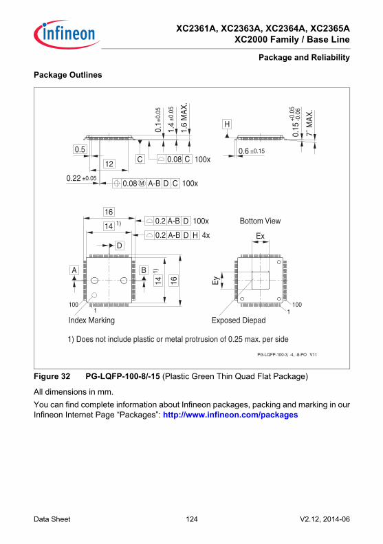
XC2361A, XC2363A, XC2364A, XC2365AXC2000 Family / Base Line
Package and Reliability
Data Sheet 124 V2.12, 2014-06
Package Outlines
Figure 32 PG-LQFP-100-8/-15 (Plastic Green Thin Quad Flat Package)
All dimensions in mm.You can find complete information about Infineon packages, packing and marking in ourInfineon Internet Page “Packages”: http://www.infineon.com/packages
1) Does not include plastic or metal protrusion of 0.25 max. per side
PG-LQFP-100-3, -4, -8-PO V11
0.5
12
0.22A-B0.08 M C
C
D 100x
100x
±0.051.
6 M
AX
.
±0.0
5
±0.0
5C
0.1
0.081.
4
±0.150.6
H
7˚ M
AX
.
+0.0
5-0
.06
0.15
A B
Index Marking1
100
D
14 1)
160.2 A-B D 100x
4xDA-B0.2 H
141)
16
Bottom View
1001
Exposed Diepad
Ey
Ex

XC2361A, XC2363A, XC2364A, XC2365AXC2000 Family / Base Line
Package and Reliability
Data Sheet 125 V2.12, 2014-06
5.2 Thermal ConsiderationsWhen operating the XC236xA in a system, the total heat generated in the chip must bedissipated to the ambient environment to prevent overheating and the resulting thermaldamage.The maximum heat that can be dissipated depends on the package and its integrationinto the target board. The “Thermal resistance RΘJA” quantifies these parameters. Thepower dissipation must be limited so that the average junction temperature does notexceed 150 °C.The difference between junction temperature and ambient temperature is determined byΔT = (PINT + PIOSTAT + PIODYN) × RΘJA
The internal power consumption is defined asPINT = VDDP × IDDP (switching current and leakage current).The static external power consumption caused by the output drivers is defined asPIOSTAT = Σ((VDDP-VOH) × IOH) + Σ(VOL × IOL)The dynamic external power consumption caused by the output drivers (PIODYN) dependson the capacitive load connected to the respective pins and their switching frequencies.If the total power dissipation for a given system configuration exceeds the defined limit,countermeasures must be taken to ensure proper system operation:• Reduce VDDP, if possible in the system• Reduce the system frequency• Reduce the number of output pins• Reduce the load on active output drivers

XC2361A, XC2363A, XC2364A, XC2365AXC2000 Family / Base Line
Package and Reliability
Data Sheet 126 V2.12, 2014-06
5.3 Quality DeclarationsThe operation lifetime of the XC236xA depends on the applied temperature profile in theapplication. For a typical example, please refer to Table 42; for other profiles, pleasecontact your Infineon counterpart to calculate the specific lifetime within your application.
Table 41 Quality ParametersParameter Symbol Values Unit Note /
Test ConditionMin. Typ. Max.Operation lifetime tOP CC − − 20 a See Table 42
and Table 43ESD susceptibility according to Human Body Model (HBM)
VHBM SR
− − 2 000 V EIA/JESD22-A114-B
Moisture sensitivity level MSL CC − − 3 − JEDECJ-STD-020C
Table 42 Typical Usage Temperature ProfileOperating Time (Sum = 20 years) Operating Temperat. Notes1 200 h TJ = 150°C Normal operation3 600 h TJ = 125°C Normal operation7 200 h TJ = 110°C Normal operation12 000 h TJ = 100°C Normal operation7 × 21 600 h TJ = 0…10°C, …,
60…70°CPower reduction
Table 43 Long Time Storage Temperature ProfileOperating Time (Sum = 20 years) Operating Temperat. Notes2 000 h TJ = 150°C Normal operation16 000 h TJ = 125°C Normal operation6 000 h TJ = 110°C Normal operation151 200 h TJ ≤ 150°C No operation