Embed Size (px)
Citation preview
1
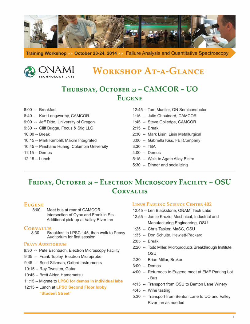
Thursday, October 23 ~ CAMCOR ~ UO Eugene
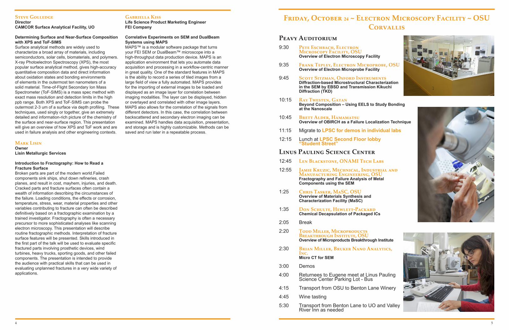
Friday, October 24 ~ Electron Microscopy Facility ~ OSU Corvallis
Workshop At-a-Glance
8:00 -- Breakfast8:40 -- Kurt Langworthy, CAMCOR9:00 -- Jeff Ditto, University of Oregon9:30 -- Cliff Bugge, Focus & Stig LLC10:00 -- Break10:15 -- Mark Kimball, Maxim Integrated10:45 -- Pinshane Huang, Columbia University11:15 -- Demos12:15 -- Lunch
Eugene 8:00 Meet bus at rear of CAMCOR,
intersection of Oynx and Franklin Sts. Additional pick-up at Valley River Inn
Corvallis 8:30 Breakfast in LPSC 145, then walk to Peavy
Auditorium for first session
Peavy Auditorium9:30 -- Pete Eschbach, Electron Microscopy Facility9:35 -- Frank Tepley, Electron Microprobe9:45 -- Scott Sitzman, Oxford Instruments10:15 -- Ray Twesten, Gatan10:45 -- Brett Alder, Hamamatsu11:15 -- Migrate to LPSC for demos in individual labs12:15 -- Lunch at LPSC Second Floor lobby
“Student Street”
Training Workshop > > October 23-24, 2014 > > Failure Analysis and Quantitative Spectroscopy
12:45 -- Tom Mueller, ON Semiconductor1:15 -- Julie Chouinard, CAMCOR1:45 -- Steve Golledge, CAMCOR2:15 -- Break2:30 -- Mark Lisin, Lisin Metallurgical3:00 -- Gabriella Kiss, FEI Company3:30 -- TBA4:00 -- Demos5:15 -- Walk to Agate Alley Bistro5:30 -- Dinner and socializing
Linus Pauling Science Center 40212:45 -- Len Blackstone, ONAMI Tech Labs12:55 -- Jamie Kruzic, Mechnical, Industrial and
Manufacturing Engineering, OSU 1:25 -- Chris Tasker, MaSC, OSU1:35 -- Don Schulte, Hewlett-Packard2:05 -- Break2:20 -- Todd Miller, Microproducts Breakthrough Institute,
OSU2:30 -- Brian Miller, Bruker3:00 -- Demos4:00 -- Returnees to Eugene meet at EMF Parking Lot
- Bus4:15 -- Transport from OSU to Benton Lane Winery4:45 -- Wine tasting5:30 -- Transport from Benton Lane to UO and Valley
River Inn as needed
2 3
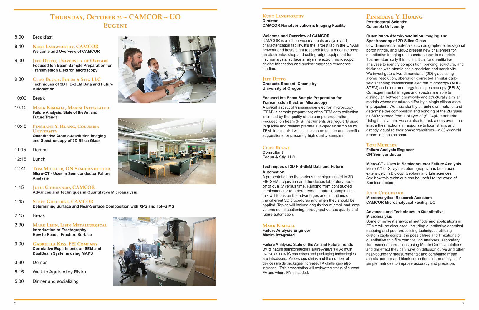
8:00 Breakfast
8:40 Kurt Langworthy, CAMCOR Welcome and Overview of CAMCOR
9:00 Jeff Ditto, University of Oregon
Focused Ion Beam Sample Preparation for Transmission Electron Microscopy
9:30 Cliff Bugge, Focus & Stig LLC Techniques of 3D FIB-SEM Data and Future Automation
10:00 Break
10:15 Mark Kimball, Maxim Integrated Failure Analysis: State of the Art and Future Trends
10:45 Pinshane Y. Huang, Columbia University Quantitative Atomic-resolution Imaging and Spectroscopy of 2D Silica Glass
11:15 Demos
12:15 Lunch
12:45 Tom Mueller, ON Semiconductor Micro-CT - Uses in Semiconductor Failure Analysis
1:15 Julie Chouinard, CAMCOR Advances and Techniques in Quantitative Microanalysis
1:45 Steve Golledge, CAMCOR Determining Surface and Near-Surface Composition with XPS and ToF-SIMS
2:15 Break
2:30 Mark Lisin, Lisin Metallurgical Introduction to Fractography: How to Read a Fracture Surface
3:00 Gabriella Kiss, FEI Company Correlative Experiments on SEM and DualBeam Systems using MAPS
3:30 Demos 5:15 Walk to Agate Alley Bistro
5:30 Dinner and socializing
Thursday, October 23 ~ CAMCOR ~ UO Eugene
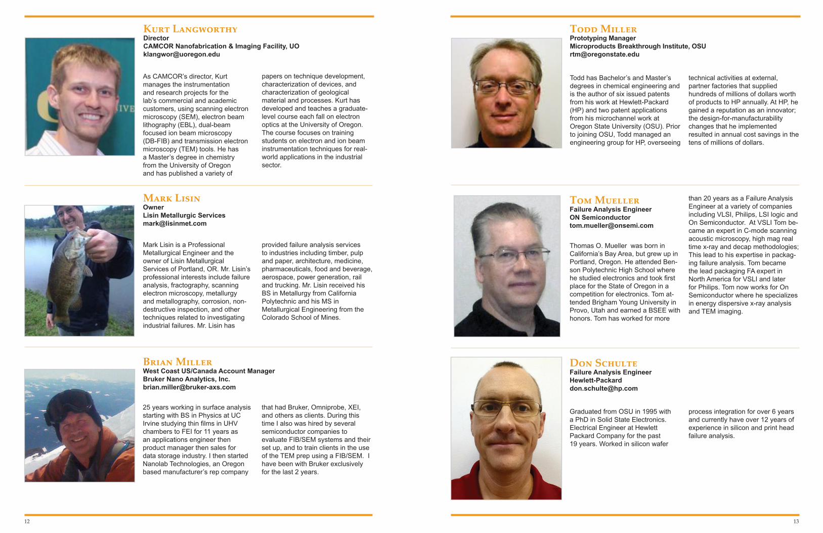
Kurt LangworthyDirectorCAMCOR Nanofabrication & Imaging Facility
Welcome and Overview of CAMCOR CAMCOR is a full-service materials analysis and characterization facility. It’s the largest lab in the ONAMI network and hosts eight research labs, a machine shop, an electronics shop and cutting-edge equipment for microanalysis, surface analysis, electron microscopy, device fabrication and nuclear magnetic resonance studies.
Jeff DittoGraduate Student, ChemistryUniversity of Oregon
Focused Ion Beam Sample Preparation for Transmission Electron MicroscopyA critical aspect of transmission electron microscopy (TEM) is sample preparation; often TEM data collection is limited by the quality of the sample preparation. Focused ion beam (FIB) instruments are regularly used to quickly and reliably prepare site-specific samples for TEM. In this talk I will discuss some unique and specific suggestions for preparing high quality samples.
Cliff BuggeConsultantFocus & Stig LLC
Techniques of 3D FIB-SEM Data and Future AutomationA presentation on the various techniques used in 3D FIB-SEM acquisition and the classic laboratory trade off of quality versus time. Ranging from constructed semiconductor to heterogeneous natural samples this talk will focus on the advantages and limitations of the different 3D procedures and when they should be applied. Topics will include acquisition of small and large volume serial sectioning, throughput versus quality and future automation.
Mark KimballFailure Analysis EngineerMaxim Integrated
Failure Analysis: State of the Art and Future TrendsBy its nature semiconductor Failure Analysis (FA) must evolve as new IC processes and packaging technologies are introduced. As devices shrink and the number of devices inside packages increase, FA challenges also increase. This presentation will review the status of current FA and where FA is headed.
Pinshane Y. HuangPostdoctoral ScientistColumbia University
Quantitative Atomic-resolution Imaging and Spectroscopy of 2D Silica GlassLow-dimensional materials such as graphene, hexagonal boron nitride, and MoS2 present new challenges for quantitative imaging and spectroscopy: in materials that are atomically thin, it is critical for quantitative analyses to identify composition, bonding, structure, and thickness with atomic-scale precision and sensitivity. We investigate a two-dimensional (2D) glass using atomic resolution, aberration-corrected annular dark-field scanning transmission electron microscopy (ADF-STEM) and electron energy-loss spectroscopy (EELS). Our experimental images and spectra are able to distinguish between chemically and structurally similar models whose structures differ by a single silicon atom in projection. We thus identify an unknown material and determine the composition and bonding of the 2D glass as SiO2 formed from a bilayer of (SiO4)4- tetrahedra. Using this system, we are also to track atoms over time, image their motions in response to local strain, and directly visualize their phase transitions—a 80-year-old dream in glass science.
Tom MuellerFailure Analysis EngineerON Semiconductor
Micro-CT - Uses in Semiconductor Failure AnalysisMicro-CT or X-ray microtomography has been used extensively in Biology, Geology and Life sciences. See how this technique can be useful to the world of Semiconductors.
Julie Chouinard Microanalytical Research AssistantCAMCOR Microanalytical Facility, UO
Advances and Techniques in Quantitative MicroanalysisSome of newest analytical methods and applications in EPMA will be discussed, including quantitative chemical mapping and post-processing techniques utilizing customizable scripts; the possibilities and limitations of quantitative thin film composition analyses; secondary fluorescence corrections using Monte Carlo simulations and the effect they can have on diffusion curve and other near-boundary measurements; and combining mean atomic number and blank corrections in the analysis of simple matrices to improve accuracy and precision.
4 5
Steve GolledgeDirectorCAMCOR Surface Analytical Facility, UO
Determining Surface and Near-Surface Composition with XPS and ToF-SIMSSurface analytical methods are widely used to characterize a broad array of materials, including semiconductors, solar cells, biomaterials, and polymers. X-ray Photoelectron Spectroscopy (XPS), the most popular surface analytical method, gives high-accuracy quantitative composition data and direct information about oxidation states and bonding environments of elements in the outermost ten nanometers of a solid material. Time-of-Flight Secondary Ion Mass Spectrometer (ToF-SIMS) is a mass spec method with exact mass resolution and detection limits in the high ppb range. Both XPS and ToF-SIMS can probe the outermost 2-3 um of a surface via depth profiling. These techniques, used singly or together, give an extremely detailed and information-rich picture of the chemistry of the surface and near-surface region. This presentation will give an overview of how XPS and ToF work and are used in failure analysis and other engineering contexts.
Mark LisinOwnerLisin Metallurgic Services
Introduction to Fractography: How to Read a Fracture SurfaceBroken parts are part of the modern world.Failed components sink ships, shut down refineries, crash planes, and result in cost, mayhem, injuries, and death. Cracked parts and fracture surfaces often contain a wealth of information describing the circumstances of the failure. Loading conditions, the effects or corrosion, temperature, stress, wear, material properties and other variables contributing to fracture can often be described definitively based on a fractographic examination by a trained investigator. Fractography is often a necessary precursor to more sophisticated analyses like scanning electron microscopy. This presentation will describe routine fractographic methods. Interpretation of fracture surface features will be presented. Skills introduced in the first part of the talk will be used to evaluate specific fractured parts involving prosthetic devices, wind turbines, heavy trucks, sporting goods, and other failed components. The presentation is intended to provide the audience with practical skills that can be used in evaluating unplanned fractures in a very wide variety of applications.
Gabriella KissLife Science Product Marketing EngineerFEI Company
Correlative Experiments on SEM and DualBeam Systems using MAPSMAPS™ is a modular software package that turns your FEI SEM or DualBeam™ microscope into a high-throughput data production device. MAPS is an application environment that lets you automate data acquisition and processing in a workflow-centric manner in great quality. One of the standard features in MAPS is the ability to record a series of tiled images from a large field of view a fully automated. MAPS provides for the importing of external images to be loaded and displayed as an image layer for correlation between imaging modalities. The layer can be displayed, hidden or overlayed and correlated with other image layers. MAPS also allows for the correlation of the signals from different detectors. In this case, the correlation between backscattered and secondary electron imaging can be examined. MAPS handles data acquisition, presentation, and storage and is highly customizable. Methods can be saved and run later in a repeatable process.
Peavy Auditorium9:30 Pete Eschbach, Electron
Microscopy Facility, OSU Overview of Electron Microscopy Facility
9:35 Frank Tepley, Electron Microprobe, OSU Overview of Electron Microprobe Facility
9:45 Scott Sitzman, Oxford Instruments Diffraction-based Microstructural Characterization in the SEM by EBSD and Transmission Kikuchi Diffraction (TKD)
10:15 Ray Twesten, Gatan Beyond Composition – Using EELS to Study Bonding at the Nanoscale
10:45 Brett Alder, Hamamatsu Overview of OBIRCH as a Failure Localization Technique
11:15 Migrate to LPSC for demos in individual labs
12:15 Lunch at LPSC Second Floor lobby “Student Street”
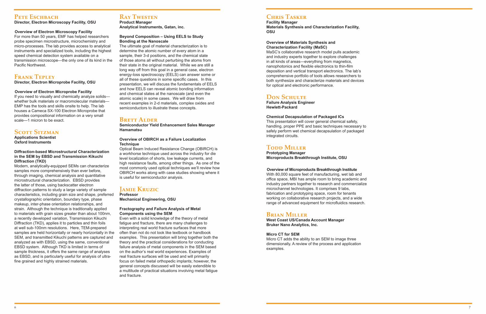
Linus Pauling Science Center12:45 Len Blackstone, ONAMI Tech Labs
12:55 Jamie Kruzic, Mechnical, Industrial and Manufacturing Engineering, OSU Fractography and Failure Analysis of Metal Components using the SEM
1:25 Chris Tasker, MaSC, OSU
Overview of Materials Synthesis and Characterization Facility (MaSC)
1:35 Don Schulte, Hewlett-Packard Chemical Decapsulation of Packaged ICs
2:05 Break
2:20 Todd Miller, Microproducts Breakthrough Institute, OSU Overview of Microproducts Breakthrough Institute
2:30 Brian Miller, Bruker Nano Analytics, Inc. Micro CT for SEM
3:00 Demos
4:00 Returnees to Eugene meet at Linus Pauling Science Center Parking Lot - Bus
4:15 Transport from OSU to Benton Lane Winery
4:45 Wine tasting
5:30 Transport from Benton Lane to UO and Valley River Inn as needed
Friday, October 24 ~ Electron Microscopy Facility ~ OSU Corvallis
6 7
Pete EschbachDirector, Electron Microscopy Facility, OSU
Overview of Electron Microscopy FacilityFor more than 50 years, EMF has helped researchers probe specimen microstructure, microchemistry and micro-processes. The lab provides access to analytical instruments and specialized tools, including the highest speed chemical detection system available on a transmission microscope—the only one of its kind in the Pacific Northwest.
Frank TepleyDirector, Electron Microprobe Facility, OSU
Overview of Electron Microprobe FacilityIf you need to visually and chemically analyze solids—whether bulk materials or macromolecular materials—EMP has the tools and skills onsite to help. The lab houses a Cameca SX-100 Electron Microprobe that provides compositional information on a very small scale—1 micron to be exact.
Scott SitzmanApplications ScientistOxford Instruments
Diffraction-based Microstructural Characterization in the SEM by EBSD and Transmission Kikuchi Diffraction (TKD)Modern, analytically-equipped SEMs can characterize samples more comprehensively than ever before, through imaging, chemical analysis and quantitative microstructural characterization. EBSD provides the latter of those, using backscatter electron diffraction patterns to study a large variety of sample characteristics, including grain size and shape, preferred crystallographic orientation, boundary type, phase makeup, inter-phase orientation relationships, and strain. Although the technique is traditionally applied to materials with grain sizes greater than about 100nm, a recently developed variation, Transmission Kikuchi Diffraction (TKD), applies it to particles and thin foils at well sub-100nm resolutions. Here, TEM-prepared samples are held horizontally or nearly horizontally in the SEM, and transmitted Kikuchi patterns are captured and analyzed as with EBSD, using the same, conventional EBSD system. Although TKD is limited in terms of sample thickness, it offers the same range of analyses as EBSD, and is particularly useful for analysis of ultra-fine grained and highly strained materials.
Ray TwestenProduct ManagerAnalytical Instruments, Gatan, inc.
Beyond Composition – Using EELS to Study Bonding at the NanoscaleThe ultimate goal of material characterization is to determine the atomic number of every atom in a sample, their 3-d positions, and the chemical state of those atoms all without perturbing the atoms from their state in the original material. While we are still a long way off from this goal in a general case, electron energy-loss spectroscopy (EELS) can answer some or all of these questions in some specific cases. In this presentation, we will discuss the fundamentals of EELS and how EELS can reveal atomic bonding information and chemical states at the nanoscale (and even the atomic scale) in some cases. We will draw from recent examples in 2-d materials, complex oxides and semiconductors to illustrate these concepts.
Brett AlderSemiconductor Yield Enhancement Sales Manager Hamamatsu
Overview of OBIRCH as a Failure Localization TechniqueOptical Beam Induced Resistance Change (OBIRCH) is a workhorse technique used across the industry for die level localization of shorts, low leakage currents, and high resistance faults, among other things. As one of the most commonly used optical techniques we’ll review how OBIRCH works along with case studies showing where it is useful for semiconductor analysis.
Jamie KruzicProfessorMechanical Engineering, OSU
Fractography and Failure Analysis of Metal Components using the SEMEven with a solid knowledge of the theory of metal fatigue and fracture, there are many challenges to interpreting real world fracture surfaces that more often than not do not look like textbook or handbook examples. This presentation will bring together both the theory and the practical considerations for conducting failure analysis of metal components in the SEM based on the author’s real world experiences. Examples of real fracture surfaces will be used and will primarily focus on failed metal orthopedic implants; however, the general concepts discussed will be easily extendible to a multitude of practical situations involving metal fatigue and fracture.
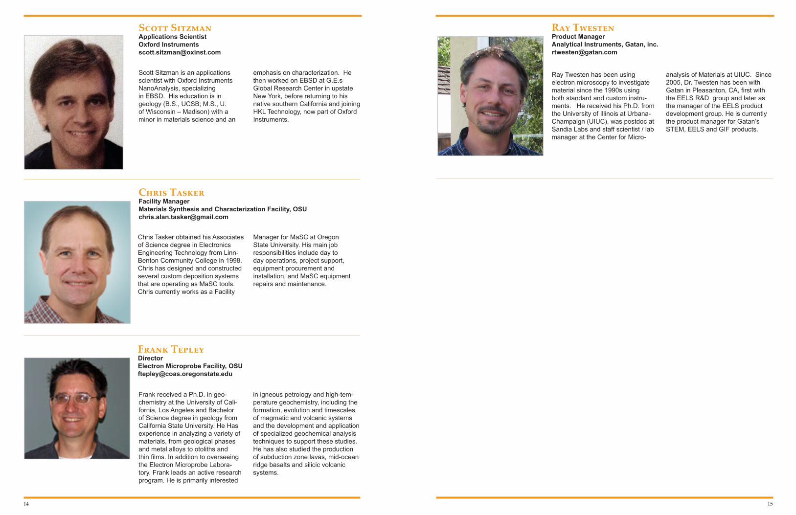
Chris TaskerFacility ManagerMaterials Synthesis and Characterization Facility, OSU
Overview of Materials Synthesis and Characterization Facility (MaSC)MaSC’s collaborative research model pulls academic and industry experts together to explore challenges in all kinds of areas—everything from magnetics, nanophotonics and flexible electronics to thin-film deposition and vertical transport electronics. The lab’s comprehensive portfolio of tools allows researchers to both synthesize and characterize materials and devices for optical and electronic performance.
Don SchulteFailure Analysis EngineerHewlett-Packard
Chemical Decapsulation of Packaged ICsThis presentation will cover general chemical safety, handling, proper PPE and basic techniques necessary to safely perform wet chemical decapsulation of packaged integrated circuits.
Todd MillerPrototyping ManagerMicroproducts Breakthrough Institute, OSU
Overview of Microproducts Breakthrough InstituteWith 80,000 square feet of manufacturing, wet lab and office space, MBI has ample room to bring academic and industry partners together to research and commercialize microchannel technologies. It comprises 9 labs, fabrication and prototyping space, room for tenants working on collaborative research projects, and a wide range of advanced equipment for microfluidics research.
Brian MillerWest Coast US/Canada Account ManagerBruker Nano Analytics, Inc.
Micro CT for SEMMicro CT adds the ability to an SEM to image three dimensionally. A review of the process and application examples.
8 9
Brett AlderSemiconductor Yield Enhancement Sales Manager [email protected]
Len BlackstoneDirectorONAMI Technology [email protected]
Len assists ONAMI’s signature research universities connect with industry, while also helping busi-nesses develop and introduce new products, acquire new customers, increase sales, and expand into new markets. He has helped companies grow for over 30 years, working with-Fortune 500 companies and entre-preneurial startups—both for-profits and non-profits. He is a master marketer whose work has gained
Cliff BuggeConsultantFocus & Stig [email protected]
With 18 years of FIB-SEM experience Cliff is currently working as a consultant with an exploration and development group to advance the 2D and 3D work flow of a production lab. Prior experience includes 9 years with a local
Julie Chouinard Microanalytical Research AssistantCAMCOR Microanalytical Facility, [email protected]
Julie has a B.A. and M.S. in earth science and has been working in the
Jeff DittoGraduate Student, ChemistryUniversity of [email protected]
Jeff Ditto worked at the University of Oregon for 5 years helping manage the scanning electron microscope and focused ion beam facilities. Jeff
ONAMI Workshop Presenters’ Biosketches
national media attention such as on 60 Minutes. He has been a college instructor and is a recurring guest lecturer at major universities. Len is an expert at exploring and assessing new market opportunities, identify-ing effective marketing strategies and developing go-to-market tactics. Prior to starting his consulting firm in 2001, Len worked in advertising and sales promotion, leading numerous national and international marketing campaigns. He has expertise in sev-eral industries, including technology, life sciences, biotech, health care, medical devices and consumer pack-age goods.
Hamamatsu is a 60 year old Photonics company and early pioneer in photoemission microscopy.
Brett Alder has 9 years of technical sales experience in the photonics industry and is the
Business Development Manager for Hamamatsu Semiconductor Analysis instruments. He specializes in co-developing new analysis techniques with U.S. companies and preparing those techniques for commercialization.
is currently a graduate student in the Department of Chemistry at the University of Oregon.
MicroAnalytical Facility in CAMCOR since 2011.
semiconductor failure analysis lab as well as 7 years of applications and testing with a microscope vendor. Cliff has a Bachelor of Science in Geology from Portland State University 1996.
10 11
Jamie KruzicProfessorMechanical Engineering, [email protected]
Dr. Jamie Kruzic is a professor of Mechanical Engineering and Materials Science at Oregon State University, where he has been on the faculty since 2004. He holds Ph.D. and M.S. degrees in Material Science and Engineering from the University of California, Berkeley, and a B.S. degree in Materials Science and Engineering from the University of Illinois, Urbana-Champaign. His field
Gabriella KissLife Science Product Marketing EngineerFEI [email protected]
Gabriella Kiss has finished her masters at Szeged University in Hungary in the field of Biotechnology. She completed a 2 years laboratory based internship focusing on the characterization of renewable energy using molecular and microbiological techniques. After finishing her gradu-ate studies, she accepted a PhD scholarship at University of Reading in UK. With Benjamin Neuman as her
Mark KimballFailure Analysis EngineerMaxim [email protected]
Mark received his BSEE and MSEE degrees at the University of Idaho. Mark has been involved in the field of failure analysis for 40 years, spending the first 20 at Tektronix and is currently at Maxim Integrated in
Pete EschbachDirectorElectron Microscopy Facility, [email protected]
Peter received a Ph.D. in materials science from Washington State University. Prior to coming to Oregon State University, he worked for Pacific Northwest Laboratory in lasers and optics and at Hewlett Packard in failure analysis, working with both optical and electron microscopes. Peter specializes
Steve GolledgeDirectorCAMCOR Surface Analytical Facility, [email protected]
Pinshane Y. HuangPostdoctoral ScientistColumbia [email protected]
Pinshane Y. Huang is a postdoctoral scientist at in the Materials Research Center of Columbia University. Her research focuses around atom-by-atom imaging and spectroscopy of two-dimensional materials such as graphene. She has earned a Ph.D. in Applied Physics from Cornell
Stephen Golledge received his Ph.D. in Materials Science and Engineering from The Johns Hopkins University. He took his first XPS spectrum as a graduate student in the mid 80’s, and began working with ToF-SIMS intensely in 1995. In the intervening years he has
used both methods to characterize an astonishing variety of materials ranging from chainsaw blades to IR detection arrays, and has trained over two hundred undergraduate, graduate, and post-doctoral level researchers in the operation of the instrumentation.
supervisor, she completed her PhD in molecular virology. She was studying the structure of corona- and influenza viruses using cryo-electron micros-copy and single particle analysis. The main focus of her studies was to find the universal role of matrix proteins in these different enveloped viruses. Then to further understand virus organization, she took a postdoctoral fellowship at Emory University in Atlanta, USA. There she was study-ing various paramyxoviruses using cryo-tomography under the supervi-sion of Elizabeth Wright. This year, she joined FEI where she supports life science customers in electron microscopy applications as PME.
of scholarly research focuses on the deformation, fracture, and fatigue behavior of materials and he has authored or co-authored more than 90 peer reviewed publications on these subjects. His research has led to numerous awards including the prestigious National Science Foundation CAREER Award in the USA and the Friedrich Wilhelm Bessel Research Award in Germany. In addition to his academic research background, Dr. Kruzic has more than 12 years experience in failure analysis consulting, primarily for the biomedical device industry.
in SEM FIB preparation, having honed his skills under the tutelage of Ron Kelley (now with FEI) and Randy Burgess (HP). He extended his expertise with formal training in Lehigh University’s STEM, EDAX EBSD and Gatan EELS/EFTEM courses.
University under the guidance of David A. Muller. She also holds a B.A. in Physics from Carleton College. Her work has been featured in National Geographic, BusinessWeek, CBS News, Discover Magazine, and the Guinness Book of World Records.
Hillsboro, Oregon. He has authored a number of papers on different aspects of Failure Analysis and has served as Co-Chair for ISTFA (the International Society for Test and Failure Analysis) for the past 5 years.
12 13
Mark LisinOwnerLisin Metallurgic [email protected]
Brian MillerWest Coast US/Canada Account ManagerBruker Nano Analytics, [email protected]
25 years working in surface analysis starting with BS in Physics at UC Irvine studying thin films in UHV chambers to FEI for 11 years as an applications engineer then product manager then sales for data storage industry. I then started Nanolab Technologies, an Oregon based manufacturer’s rep company
Mark Lisin is a Professional Metallurgical Engineer and the owner of Lisin Metallurgical Services of Portland, OR. Mr. Lisin’s professional interests include failure analysis, fractography, scanning electron microscopy, metallurgy and metallography, corrosion, non-destructive inspection, and other techniques related to investigating industrial failures. Mr. Lisin has
Todd MillerPrototyping ManagerMicroproducts Breakthrough Institute, [email protected]
Todd has Bachelor’s and Master’s degrees in chemical engineering and is the author of six issued patents from his work at Hewlett-Packard (HP) and two patent applications from his microchannel work at Oregon State University (OSU). Prior to joining OSU, Todd managed an engineering group for HP, overseeing
Tom MuellerFailure Analysis EngineerON [email protected]
Thomas O. Mueller was born in California’s Bay Area, but grew up in Portland, Oregon. He attended Ben-son Polytechnic High School where he studied electronics and took first place for the State of Oregon in a competition for electronics. Tom at-tended Brigham Young University in Provo, Utah and earned a BSEE with honors. Tom has worked for more
Kurt LangworthyDirectorCAMCOR Nanofabrication & Imaging Facility, [email protected]
As CAMCOR’s director, Kurt manages the instrumentation and research projects for the lab’s commercial and academic customers, using scanning electron microscopy (SEM), electron beam lithography (EBL), dual-beam focused ion beam microscopy (DB-FIB) and transmission electron microscopy (TEM) tools. He has a Master’s degree in chemistry from the University of Oregon and has published a variety of
papers on technique development, characterization of devices, and characterization of geological material and processes. Kurt has developed and teaches a graduate-level course each fall on electron optics at the University of Oregon. The course focuses on training students on electron and ion beam instrumentation techniques for real-world applications in the industrial sector.
provided failure analysis services to industries including timber, pulp and paper, architecture, medicine, pharmaceuticals, food and beverage, aerospace, power generation, rail and trucking. Mr. Lisin received his BS in Metallurgy from California Polytechnic and his MS in Metallurgical Engineering from the Colorado School of Mines.
that had Bruker, Omniprobe, XEI, and others as clients. During this time I also was hired by several semiconductor companies to evaluate FIB/SEM systems and their set up, and to train clients in the use of the TEM prep using a FIB/SEM. I have been with Bruker exclusively for the last 2 years.
technical activities at external, partner factories that supplied hundreds of millions of dollars worth of products to HP annually. At HP, he gained a reputation as an innovator; the design-for-manufacturability changes that he implemented resulted in annual cost savings in the tens of millions of dollars.
than 20 years as a Failure Analysis Engineer at a variety of companies including VLSI, Philips, LSI logic and On Semiconductor. At VSLI Tom be-came an expert in C-mode scanning acoustic microscopy, high mag real time x-ray and decap methodologies; This lead to his expertise in packag-ing failure analysis. Tom became the lead packaging FA expert in North America for VSLI and later for Philips. Tom now works for On Semiconductor where he specializes in energy dispersive x-ray analysis and TEM imaging.
Don SchulteFailure Analysis [email protected]
Graduated from OSU in 1995 with a PhD in Solid State Electronics. Electrical Engineer at Hewlett Packard Company for the past 19 years. Worked in silicon wafer
process integration for over 6 years and currently have over 12 years of experience in silicon and print head failure analysis.
14 15
Ray TwestenProduct ManagerAnalytical Instruments, Gatan, [email protected]
Ray Twesten has been using electron microscopy to investigate material since the 1990s using both standard and custom instru-ments. He received his Ph.D. from the University of Illinois at Urbana-Champaign (UIUC), was postdoc at Sandia Labs and staff scientist / lab manager at the Center for Micro-
Chris TaskerFacility ManagerMaterials Synthesis and Characterization Facility, [email protected]
Chris Tasker obtained his Associates of Science degree in Electronics Engineering Technology from Linn-Benton Community College in 1998. Chris has designed and constructed several custom deposition systems that are operating as MaSC tools. Chris currently works as a Facility
Frank TepleyDirectorElectron Microprobe Facility, [email protected]
Frank received a Ph.D. in geo-chemistry at the University of Cali-fornia, Los Angeles and Bachelor of Science degree in geology from California State University. He Has experience in analyzing a variety of materials, from geological phases and metal alloys to otoliths and thin films. In addition to overseeing the Electron Microprobe Labora-tory, Frank leads an active research program. He is primarily interested
Scott SitzmanApplications ScientistOxford [email protected]
Scott Sitzman is an applications scientist with Oxford Instruments NanoAnalysis, specializing in EBSD. His education is in geology (B.S., UCSB; M.S., U. of Wisconsin – Madison) with a minor in materials science and an
Manager for MaSC at Oregon State University. His main job responsibilities include day to day operations, project support, equipment procurement and installation, and MaSC equipment repairs and maintenance.
in igneous petrology and high-tem-perature geochemistry, including the formation, evolution and timescales of magmatic and volcanic systems and the development and application of specialized geochemical analysis techniques to support these studies. He has also studied the production of subduction zone lavas, mid-ocean ridge basalts and silicic volcanic systems.
analysis of Materials at UIUC. Since 2005, Dr. Twesten has been with Gatan in Pleasanton, CA, first with the EELS R&D group and later as the manager of the EELS product development group. He is currently the product manager for Gatan’s STEM, EELS and GIF products.
emphasis on characterization. He then worked on EBSD at G.E.s Global Research Center in upstate New York, before returning to his native southern California and joining HKL Technology, now part of Oxford Instruments.